Embed Size (px)
Citation preview

A Low-Power Quadrature Digital Modulator
in 0.18µm CMOS
A Thesis Submitted to the College of
Graduate Studies and Research
in Partial Fulfillment of the Requirements
for the Degree of Master of Science
in the Department of Electrical and Computer Engineering
University of Saskatchewan
Saskatoon, Saskatchewan
by
Song Hu
c© Copyright Song Hu, April 2007. All rights reserved.

PERMISSION TO USE
In presenting this thesis in partial fulfilment of the requirements for a Postgraduate
degree from the University of Saskatchewan, I agree that the Libraries of this Uni-
versity may make it freely available for inspection. I further agree that permission
for copying of this thesis in any manner, in whole or in part, for scholarly purposes
may be granted by the professor or professors who supervised my thesis work or, in
their absence, by the Head of the Department or the Dean of the College in which
my thesis work was done. It is understood that any copying or publication or use
of this thesis or parts thereof for financial gain shall not be allowed without my
written permission. It is also understood that due recognition shall be given to me
and to the University of Saskatchewan in any scholarly use which may be made of
any material in my thesis.
Requests for permission to copy or to make other use of material in this thesis in
whole or part should be addressed to:
Head of the Department of Electrical and Computer Engineering
University of Saskatchewan
Saskatoon, Saskatchewan, Canada
S7N 5A9
i
ABSTRACT
Quadrature digital modulation techniques are widely used in modern commu-
nication systems because of their high performance and flexibility. However, these
advantages come at the cost of high power consumption. As a result, power con-
sumption has to be taken into account as a main design factor of the modulator.
In this thesis, a low-power quadrature digital modulator in 0.18µm CMOS is
presented with the target system clock speed of 150 MHz. The quadrature digi-
tal modulator consists of several key blocks: quadrature direct digital synthesizer
(QDDS), pulse shaping filter, interpolation filter and inverse sinc filter. The design
strategy is to investigate different implementations for each block and compare the
power consumption of these implementations. Based on the comparison results,
the implementation that consumes the lowest power will be chosen for each block.
First of all, a novel low-power QDDS is proposed in the thesis. Power consumption
estimation shows that it can save up to 60% of the power consumption at 150 MHz
system clock frequency compared with one conventional design. Power consump-
tion estimation results also show that using two pulse shaping blocks to process
I/Q data, cascaded integrator comb (CIC) interpolation structure, and inverse sinc
filter with modified canonic signed digit (MCSD) multiplication consume less power
than alternative design choices. These low-power blocks are integrated together to
achieve a low-power modulator. The power consumption estimation after layout
shows that it only consumes about 95 mW at 150 MHz system clock rate, which is
much lower than similar commercial products.
The designed modulator can provide a low-power solution for various quadrature
modulators. It also has an output bandwidth from 0 to 75 MHz, configurable pulse
shaping filters and interpolation filters, and an internal sin(x)/x correction filter.
ii

ACKNOWLEDGEMENTS
I would like to express my most special gratitude to my supervisor Professor
Daniel Teng for his patient guidance and financial support during this research.
Some discussions with him inspired me a lot, not only for this research but also for
my future professional career. Another special gratitude goes to CMC microsystems
for their software and tutorial.
I would like to thank Professor Ron Bolton who taught me VLSI class and
also gave me some suggestions for my research. I also want to thank all the other
professors who taught me classes at the University of Saskatchewan.
Finally, I would like to thank my wife, Li Sha, and my parents, Yang Guoqing
and Hu Jiyuan, for their support. Their love and patience give me a lot of faith
during some difficult times.
iii

DEDICATION
This thesis is dedicated to my wife and my parents.
iv

Contents
PERMISSION TO USE i
ABSTRACT ii
ACKNOWLEDGEMENTS iii
DEDICATION iv
TABLE OF CONTENTS v
LIST OF FIGURES ix
LIST OF TABLES xiii
ABBREVIATIONS xiv
1 Introduction 1
1.1 Research motivation . . . . . . . . . . . . . . . . . . . . . . . . . . 2
1.2 Research objectives . . . . . . . . . . . . . . . . . . . . . . . . . . . 3
1.3 Thesis outline . . . . . . . . . . . . . . . . . . . . . . . . . . . . . . 4
2 Background 5
2.1 Quadrature direct digital synthesizer . . . . . . . . . . . . . . . . . 5
2.2 Pulse shaping filter . . . . . . . . . . . . . . . . . . . . . . . . . . . 8
2.3 Interpolation filter . . . . . . . . . . . . . . . . . . . . . . . . . . . 11
2.4 Modulation . . . . . . . . . . . . . . . . . . . . . . . . . . . . . . . 16
2.5 Digital to analog converter (DAC) . . . . . . . . . . . . . . . . . . . 19
2.6 Inverse sinc filter . . . . . . . . . . . . . . . . . . . . . . . . . . . . 20
v

2.7 Summary . . . . . . . . . . . . . . . . . . . . . . . . . . . . . . . . 23
3 Integrated Circuit Design Flow 24
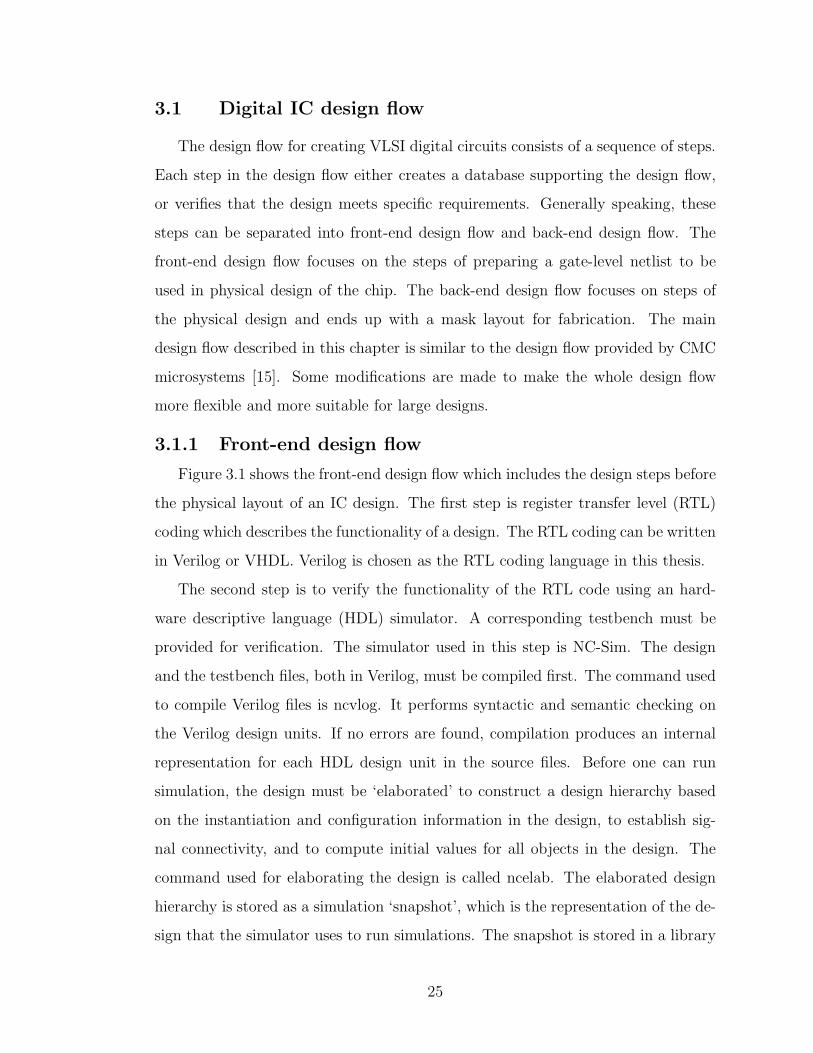
3.1 Digital IC design flow . . . . . . . . . . . . . . . . . . . . . . . . . . 25
3.1.1 Front-end design flow . . . . . . . . . . . . . . . . . . . . . . 25
3.1.2 Back-end design . . . . . . . . . . . . . . . . . . . . . . . . . 28
3.2 Summary . . . . . . . . . . . . . . . . . . . . . . . . . . . . . . . . 31
4 Circuit Design and Low Power Considerations 32
4.1 Quadrature digital modulator . . . . . . . . . . . . . . . . . . . . . 32
4.2 QDDS . . . . . . . . . . . . . . . . . . . . . . . . . . . . . . . . . . 34
4.2.1 ROM compression . . . . . . . . . . . . . . . . . . . . . . . 34
4.2.2 Quadrature outputs . . . . . . . . . . . . . . . . . . . . . . . 41
4.3 Pulse shaping filter . . . . . . . . . . . . . . . . . . . . . . . . . . . 44
4.3.1 Polyphase structure . . . . . . . . . . . . . . . . . . . . . . . 44
4.3.2 Design considerations of the pulse shaping filter . . . . . . . 45
4.3.3 Quadrature processing . . . . . . . . . . . . . . . . . . . . . 46
4.4 Interpolation filter . . . . . . . . . . . . . . . . . . . . . . . . . . . 49
4.4.1 Design of CIC filter . . . . . . . . . . . . . . . . . . . . . . . 49
4.4.2 Design of half-band filter . . . . . . . . . . . . . . . . . . . . 52
4.5 Inverse sinc filter . . . . . . . . . . . . . . . . . . . . . . . . . . . . 54
4.5.1 Multiplication for inverse sinc filter . . . . . . . . . . . . . . 57
4.5.2 Clock gating . . . . . . . . . . . . . . . . . . . . . . . . . . . 58
4.6 Multipliers . . . . . . . . . . . . . . . . . . . . . . . . . . . . . . . . 61
4.7 Summary . . . . . . . . . . . . . . . . . . . . . . . . . . . . . . . . 64
5 Performance Evaluation 65
5.1 High-level power estimation . . . . . . . . . . . . . . . . . . . . . . 65
5.1.1 Sources of power consumption . . . . . . . . . . . . . . . . . 65
5.1.2 Power estimation and analysis flow . . . . . . . . . . . . . . 66
5.1.3 Power estimation in logic synthesizer . . . . . . . . . . . . . 67
vi
5.2 Performance of QDDS . . . . . . . . . . . . . . . . . . . . . . . . . 68
5.2.1 Output spectrum . . . . . . . . . . . . . . . . . . . . . . . . 70
5.2.2 Power consumption . . . . . . . . . . . . . . . . . . . . . . . 72
5.3 Performance of pulse shaping filter . . . . . . . . . . . . . . . . . . 72
5.4 Performance of interpolation filter . . . . . . . . . . . . . . . . . . . 73
5.4.1 Frequency response . . . . . . . . . . . . . . . . . . . . . . . 74
5.4.2 Power consumption . . . . . . . . . . . . . . . . . . . . . . . 74
5.5 Performance of inverse sinc filter . . . . . . . . . . . . . . . . . . . . 77
5.6 Summary . . . . . . . . . . . . . . . . . . . . . . . . . . . . . . . . 77
6 System Integration 79
6.1 Functional verification . . . . . . . . . . . . . . . . . . . . . . . . . 79
6.1.1 Testing model . . . . . . . . . . . . . . . . . . . . . . . . . . 79
6.1.2 QDDS . . . . . . . . . . . . . . . . . . . . . . . . . . . . . . 80
6.1.3 Pulse shaping filter . . . . . . . . . . . . . . . . . . . . . . . 82
6.1.4 CIC filter . . . . . . . . . . . . . . . . . . . . . . . . . . . . 82
6.1.5 Modulator . . . . . . . . . . . . . . . . . . . . . . . . . . . . 84
6.2 Power consumption estimation . . . . . . . . . . . . . . . . . . . . . 87
6.2.1 Power consumption estimation after logic synthesis . . . . . 87
6.2.2 Power consumption estimation after layout . . . . . . . . . . 87
6.3 Summary . . . . . . . . . . . . . . . . . . . . . . . . . . . . . . . . 89
7 Conclusions 91
7.1 Conclusions . . . . . . . . . . . . . . . . . . . . . . . . . . . . . . . 92
7.2 Future work . . . . . . . . . . . . . . . . . . . . . . . . . . . . . . . 93
REFERENCES 95
APPENDICES 98
A Scripts for Digital IC Design 98
A.1 A script for invoking NCsim in batch mode . . . . . . . . . . . . . . 98
vii

A.2 A script for invoking Synopsys Design Compiler in batch mode . . . 98
A.3 A script for invoking Cadence PKS in batch mode for timing opti-
mization . . . . . . . . . . . . . . . . . . . . . . . . . . . . . . . . . 99
viii

List of Figures
1.1 Analog transmitter. . . . . . . . . . . . . . . . . . . . . . . . . . . . 2
1.2 Hybrid implementation. . . . . . . . . . . . . . . . . . . . . . . . . 2
2.1 Digital quadrature modulator. . . . . . . . . . . . . . . . . . . . . . 5
2.2 Block diagram of a basic DDS. . . . . . . . . . . . . . . . . . . . . . 6
2.3 Digital phase wheel. As the vector rotates around the wheel, a cor-
responding sine wave is being generated. . . . . . . . . . . . . . . . 6
2.4 Raised cosine pulse and spectrum. . . . . . . . . . . . . . . . . . . 9
2.5 Signal flow graph of the direct form structure FIR filter. . . . . . . 11
2.6 An example of 1-to-4 upsampling. “x” shows the input binary data
and “o” shows the output after 1-to-4 upsampling. . . . . . . . . . . 12
2.7 Output sequence of a SQRC filter. “x” shows the input binary data
and “o” shows the output sequence. . . . . . . . . . . . . . . . . . . 12
2.8 Block diagram of the CIC interpolation filter. . . . . . . . . . . . . 13
2.9 Impulse response and frequency response of a half band FIR filter
with the length of 21. . . . . . . . . . . . . . . . . . . . . . . . . . . 15
2.10 I − Q format. . . . . . . . . . . . . . . . . . . . . . . . . . . . . . . 16
2.11 QPSK constellation. . . . . . . . . . . . . . . . . . . . . . . . . . . 18
2.12 16-QAM square constellation. . . . . . . . . . . . . . . . . . . . . . 18
2.13 Conceptual block diagram of a DAC. . . . . . . . . . . . . . . . . . 20
2.14 Ideal input output characteristics for a 2 bit DAC. . . . . . . . . . . 20
2.15 Output spectrum of a real world DAC. . . . . . . . . . . . . . . . . 22
2.16 Amplitude response of the ideal inverse sinc filter. . . . . . . . . . . 22
3.1 Block diagram of the front-end design flow. . . . . . . . . . . . . . . 26
ix
3.2 One example to compare the circuit before and after scan chain in-
sertion. After adding scan circuitry, the design has two additional
inputs, sc in and sc en, and one additional output, sc out. These
extra ports will be used when the design is in scan mode. . . . . . . 29
3.3 Block diagram of the back-end design flow. . . . . . . . . . . . . . . 30
4.1 The detailed block diagram of the designed quadrature digital mod-
ulator. . . . . . . . . . . . . . . . . . . . . . . . . . . . . . . . . . . 33
4.2 ROM design using quarter-wave symmetry. . . . . . . . . . . . . . . 34
4.3 Phase wheel comparison between no phase offset and 12-LSB phase
offset. . . . . . . . . . . . . . . . . . . . . . . . . . . . . . . . . . . 35
4.4 Error comparison between no phase offset and 12-LSB phase offset. . 35
4.5 Curves of sine-phase difference, double trigonometric approximation
and QLA and the error curves of double trigonometric approximation
and QLA. . . . . . . . . . . . . . . . . . . . . . . . . . . . . . . . . 39
4.6 Sine phase to amplitude converter using QLA method. . . . . . . . 40
4.7 Errors for QLA sine phase to amplitude converter. . . . . . . . . . . 41
4.8 Proposed QDDS architecture. . . . . . . . . . . . . . . . . . . . . . 43
4.9 An efficient implementation of 1-to-k upsampling polyphase filter. . 45
4.10 An example of the SQRC impulse response. . . . . . . . . . . . . . 47
4.11 The frequency response of the SQRC filter whose impulse response
is shown in Figure 4.10. . . . . . . . . . . . . . . . . . . . . . . . . 47
4.12 Block diagram of the SQRC filter. . . . . . . . . . . . . . . . . . . . 48
4.13 Pipelined CIC interpolation filter. . . . . . . . . . . . . . . . . . . . 50
4.14 Spectral response of 1-to-4 CIC interpolator. Solid line shows the
periodic spectrum of the zero packed time series and dashed line
shows the frequency response of the CIC filter with rate change factor
of 4. . . . . . . . . . . . . . . . . . . . . . . . . . . . . . . . . . . . 51
x
4.15 Spectral response of 1-to-8 CIC interpolator. Solid line shows the
periodic spectrum of the zero packed time series and dashed line
shows the frequency response of the CIC filter with rate change factor
of 8. . . . . . . . . . . . . . . . . . . . . . . . . . . . . . . . . . . . 51
4.16 Spectral response of two cascaded half-band FIR filters. Solid line
shows the periodic spectrum of the zero packed time series and
dashed line shows the frequency response of the two cascaded half-
band FIR filters. . . . . . . . . . . . . . . . . . . . . . . . . . . . . 53
4.17 Spectral response of three cascaded half-band FIR filters. Solid
line shows the periodic spectrum of the zero packed time series and
dashed line shows the frequency response of the three cascaded half-
band FIR filters. . . . . . . . . . . . . . . . . . . . . . . . . . . . . 53
4.18 Polyphase half-band filter. . . . . . . . . . . . . . . . . . . . . . . . 54
4.19 Impulse response of the designed inverse sinc filter. . . . . . . . . . 55
4.20 Frequency responses of the sinc distortion, ISF and the combined
system. . . . . . . . . . . . . . . . . . . . . . . . . . . . . . . . . . . 55
4.21 Signal flow graph of symmetrical FIR filter. . . . . . . . . . . . . . 57
4.22 Comparison of the three different ways to implement x × h(4). . . . 59
4.23 Implementation comparison between a flip-flop without clock gating
and with clock gating. . . . . . . . . . . . . . . . . . . . . . . . . . 60
4.24 The mechanism of using latch to prevent the glitch on the gated clock
net. . . . . . . . . . . . . . . . . . . . . . . . . . . . . . . . . . . . . 61
4.25 Block diagram of DW02 mult 2 stage before register retiming and
after register retiming. . . . . . . . . . . . . . . . . . . . . . . . . . 63
5.1 Power estimation in logic synthesizer. . . . . . . . . . . . . . . . . . 68
5.2 Two conventional QDDS implementations. . . . . . . . . . . . . . . 69
5.3 Spectrum of the QDDS output (fout ≈ 0.1 × frefclk). . . . . . . . . . 71
5.4 Spectrum of the QDDS output (fout ≈ 0.104 × frefclk). . . . . . . . 71
5.5 Power consumption comparison for 3 different QDDS architectures. 72
xi

5.6 Power consumption comparison for 2 different pulse shaping filter
implementations (interpolation ratio of interpolation filter=4). . . . 73
5.7 Comparison of HBF and CIC frequency response. . . . . . . . . . . 74
5.8 Power consumption comparison for two interpolation filters with the
interpolation ratio of 4. . . . . . . . . . . . . . . . . . . . . . . . . . 75
5.9 Power consumption comparison for two interpolation filters with the
interpolation ratio of 8. . . . . . . . . . . . . . . . . . . . . . . . . . 75
5.10 Power consumption comparison for two interpolation filters with the
interpolation ratio of 16. . . . . . . . . . . . . . . . . . . . . . . . . 76
5.11 Power consumption comparison for two interpolation filters with the
interpolation ratio of 32. . . . . . . . . . . . . . . . . . . . . . . . . 76
6.1 Testing model. . . . . . . . . . . . . . . . . . . . . . . . . . . . . . 80
6.2 Spectrum of QDDS outputs. . . . . . . . . . . . . . . . . . . . . . . 81
6.3 Signal spectrum after pulse shaping filter. . . . . . . . . . . . . . . 82
6.4 Signal spectrum after CIC filter (R = 4). . . . . . . . . . . . . . . . 83
6.5 Signal spectrum after CIC filter (R=8). . . . . . . . . . . . . . . . . 83
6.6 Output signal spectrum of the designed modulator with fout ≈ 0.1×frefclk. . . . . . . . . . . . . . . . . . . . . . . . . . . . . . . . . . . 85
6.7 Output signal spectrum of the designed modulator with fout ≈ 0.104×frefclk. . . . . . . . . . . . . . . . . . . . . . . . . . . . . . . . . . . 86
6.8 Power consumption estimation of the designed modulator after logic
synthesis. . . . . . . . . . . . . . . . . . . . . . . . . . . . . . . . . 87
6.9 Layout of the designed modulator. . . . . . . . . . . . . . . . . . . . 88
6.10 Power consumption estimation of the designed modulator after layout. 89
xii
List of Tables
4.1 Comparison between different A, B, C partitions. . . . . . . . . . . 37
4.2 Comparison between various sine approximation methods to reduce
the coarse ROM output bits. . . . . . . . . . . . . . . . . . . . . . . 39
4.3 Coefficients for the designed inverse sinc filter. . . . . . . . . . . . . 56
4.4 Comparison of binary, CSD and MCSD representations for the coef-
ficients of the inverse sinc filter. . . . . . . . . . . . . . . . . . . . . 58
4.5 Verilog codes of a flip-flop without clock gating and one with clock
gating. . . . . . . . . . . . . . . . . . . . . . . . . . . . . . . . . . . 60
5.1 Power consumption comparison of ISF using CSD multiplication and
MCSD multiplication. . . . . . . . . . . . . . . . . . . . . . . . . . 77
6.1 Comparison of different modulator ICs . . . . . . . . . . . . . . . . 89
xiii

ABBREVIATIONS
ASIC Application Specific Integrated Circuit
ATE Automatic Test Equipment
ATPG Automatic Test Pattern Generation
BPF Band-Pass Filter
CIC Cascaded Integrator Comb
CMOS Complementary Metal Oxide Silicon
CSD Canonic Signed Digit
DAC Digital to Analog Converter
DDS Direct Digital Synthesizer
DRC Design Rule Check
DSP Digital Signal Processor
FFT Fast Fourier Transform
FIR Finite Impulse Response
FPGA Field Programmable Gate Array
FS Full Scale
GUI Graphical User Interface
HBF Half-Band Filter
HDL Hardware Descriptive Language
IC Integrated Circuit
IF Intermediate Frequency
IP Intellectual Property
ISF Inverse Sinc Filter
ISI Intersymbol Interference
ITRS International Technology Roadmap for Semiconductors
LO Local Oscillator
LPF Low-Pass Filter
LSB Least Significant Bit
xiv

LVS Layout Versus Schematic
MCSD Modified Canonic Signed Digit
MSB Most Significant Bit
PKS Physically Knowledgable Synthesis
QAM Quadrature Amplitude Modulation
QDDS Quadrature Direct Digital Synthesizer
QLA Quad Line Approximation
QPSK Quadrature Phase Shift Keying
RF Radio Frequency
RTL Register Transfer Level
SNR Signal to Noise Ratio
SOC System on Chip
SQRC Squared Root Raised Cosine
VGA Variable Gain Amplifier
VLSI Very Large Scale Integration
xv
Chapter 1
Introduction
Transmitter and receiver are two major components for all the communication
systems. The basic function of the transmitter is to take the information bearing
signal produced by the source of information and modify it into a form suitable
for transmission over a channel. The receiver operates on the received signal to
produce an estimate of the original information bearing signal.
Traditional designs of analog transmitter employ the use of the phase locked
loop, mixers, analog filters and amplifiers. Figure 1.1 shows an example of tradi-
tional analog transmitter. Digital baseband in-phase (I) and quadrature (Q) signals
are converted to analog signals by digital to analog converters (DAC) and then fed
into low-pass filters (LPF). Analog I/Q signals are upconverted to an intermediate
frequency (IF) by mixing with the first local oscillator which goes through a phase
splitter to provide in-phase and quadrature local oscillation (LO) signals. The out-
puts of the mixers are then summed. This IF signal is amplified, filtered and then
mixed to the radio frequency (RF) by the IF variable gain amplifier (VGA), IF
band-pass filter (BPF) and second local oscillator, respectively. The RF signal that
has been processed by RF amplifier and RF band-pass filter is then ready to be
fed to an antenna. As one can see from this figure, all the components are analog
circuits. There are several disadvantages for this analog architecture. First, analog
electronic circuits consume more space and power. Second, they are more subject
to performance variations as a result of environmental factors such as temperature
changes. Third, it is difficult to integrate these functions into one chip according
to the current technology [1].
1

I
Q
BPF BPF00 90/0
IF Filter RF Filter
LO1 LO2
VGADAC LPF
LPFDAC
Figure 1.1 Analog transmitter.
In recent years, there is an increasing trend to replace most of these analog
circuits with digital circuits and integrate them into one chip [1]. The advantage
of this approach is that full digital control of the function is maintained as far
as possible, and the limitations of analog design are minimized. Another trend
in transceiver design is trying to reduce the cost and power consumption. It is
becoming more and more important because it makes them feasible to be embedded
into more types of electronic devices.
1.1 Research motivation
The ideal radio architecture brings the digital signal processing techniques as
close as possible to the antenna. In this ideal architecture, the analog circuits are
restricted to those which can not be performed digitally, i.e., antenna, RF filter and
power amplifier. According to the newest technology, the closest towards this ideal
architecture is the hybrid implementation, as shown in Figure 1.2, which consists
of a digital subsystem and a analog subsystem. Compared with analog transceiver,
Digital
Up Conversion
Digital
Down Conversion
Base
Band
DAC
ADC BPF
BPF
BPF
BPF
To antenna
From antenna
I
I
Q
Q
LOsf
IF Filter RF Filter
Figure 1.2 Hybrid implementation.
2
this architecture offers more flexibility, longer product life and lower cost; it is also
more suitable for mass production. Devices such as digital signal processors (DSPs),
field programmable gate arrays (FPGAs) and application specific integrated circuits
(ASICs) can be used to realize the required digital functionality.
Although there are many advantages to using digital modulator in communica-
tion systems, power consumption is still a problem for high-performance quadrature
digital modulator. For example, one commercially used quadrature digital modu-
lator, AD9856 [2], consumes about 1100 mW at 150 MHz. The power consumption
is unacceptable for most of the portable applications due to the limited battery
capacity. Also, according to international technology roadmap for semiconductors
(ITRS) 2005 report,“Power consumption is an urgent, short-term challenge. How
to quickly shift from a performance-driven design procedure to a performance and
power driven design procedure has to be solved. Design issues include high level
power estimation, dynamic and leakage power reduction at different design stages
and power optimization, etc [3].” As a result, power consumption has to be taken
into account as a main design factor. Generally speaking, to achieve a low-power
integrated circuit, many low-power design techniques can be used. These techniques
can be applied at system level, algorithm level, circuit level and transistor level.
In this thesis, a fully digital modulator with low-power consumption is imple-
mented, which is intended to function as a quadrature modulator and can be used
in various portable devices where power and performance are critical. The designed
modulator consists of pulse shaping filters, interpolation filters, a quadrature direct
digital frequency synthesizer (QDDS) and an inverse sinc filter. Several low-power
techniques are used to reduce the power consumption while maintaining high per-
formance.
1.2 Research objectives
The objectives of the research work in this thesis are:
• To develop a quadrature digital modulator with less power dissipation
• To develop a novel low-power consumption QDDS that can be used in various
3
quadrature modulators and demodulators
• To investigate low-power design techniques and their application to quadrature
digital modulator
• To develop a configurable digital quadrature digital modulator with high perfor-
mance
1.3 Thesis outline
Chapter 2 reviews the principles of the digital modulator, including the prin-
ciples of QDDS, pulse shaping filter, interpolation filter, digital modulation, DAC
and inverse sinc filter.
Chapter 3 discusses integrated circuit (IC) design challenges and digital IC de-
sign flow that is used in this thesis. The main design flow described in this chapter
follows CMC Microsystems’ design flow. However, some changes have been made
to make the whole design process more flexible and efficient.
Chapter 4 covers the circuit implementation details of the modulator. For the
QDDS circuit, a novel architecture with low-power consumption is proposed. For
the other blocks, several hardware efficient design approaches are considered as the
possible choices.
Chapter 5 introduces high-level power estimation techniques and also presents
the performance comparisons for each key block with different design options. The
proposed QDDS is compared with conventional QDDS circuits. Pulse shaping filter,
interpolation filter, inverse sinc filter are also compared with different design choices.
Chapter 6 concentrates on the functional verification of the final modulator
which is implemented with the proposed QDDS and the other relatively low-power
blocks. It also covers the power consumption estimation of the whole modulator.
Chapter 7 gives conclusions and several suggestions for future work.
4
Chapter 2
Background
As shown in Figure 2.1, a quadrature digital modulator consists of several key
blocks: QDDS, pulse shaping filters, interpolation filters and inverse sinc filter.
QDDS is used to generate sine/cosine reference carrier signals. Pulse shaping filters
are used to limit the transmitting bandwidth and reduce intersymbol interference
(ISI). Interpolation filters are used to increase sampling rate and inverse sinc filter is
used to precompensate sinc distortion coming from the following DAC. This chapter
provides the background related to these key blocks.
Symbol
Gener-
ator
I
Q
QDDS Inverse
Sinc FilterDAC
Inter-
polation
Filter
Inter-
polation
Filter
Pulse
Shaping
Filter
Pulse
Shaping
Filter
Baseband IF
Figure 2.1 Digital quadrature modulator.
2.1 Quadrature direct digital synthesizer
Direct digital synthesizer (DDS) is a circuit which uses digital signal processing
technique to generate a frequency-tunable output signal referred to a fixed frequency
and high precision clock source [4]. As shown in Figure 2.2, a basic form DDS is
composed of a precise reference clock, a phase accumulator, a sine look-up table
and a DAC.
The phase accumulator can be an N bit counter that increments the stored
5
Phase
Register
Phase to
Amplitude
Converting
ROM
DAC LPF
Ref Clock
Tuning Word
N N aN dN
Phase accumulator
Figure 2.2 Block diagram of a basic DDS.
N2
2
MN2
2
Figure 2.3 Digital phase wheel. As the vector rotates aroundthe wheel, a corresponding sine wave is being gen-erated.
number each time it receives a clock pulse. Figure 2.3 shows the diagram of digital
phase wheel. The magnitude of the increment is determined by a digital word M ,
which sets how many points to skip around the phase wheel. The larger the M ,
the faster the phase accumulator overflows and completes the equivalence of a sine
wave cycle.
The output from the phase accumulator addresses a sine look-up table which
stores sine samples to generate a digital sine wave. The following DAC generates
an analog sine wave in response to the digital input words from the sine look-up
table. Low-pass filter is used to further smooth the sine wave output from the DAC
so that a higher purity spectrum can be obtained.
6

For any tuning word M, the output frequency of the DDS is
fout = M · frefclk
2N, (2.1)
where fout is the output frequency of DDS, M is the binary tuning word, frefclk is
the reference clock frequency and N is the length in bits of the phase accumulator.
It is clear that the frequency resolution is fres =frefclk
2N .
Phase truncation is an important aspect of DDS. For example, to directly con-
vert 32 bits of phase to corresponding 8 bit amplitude would require a 4 gigabytes
ROM. It is impractical to implement such a huge ROM in a design. In real design,
the solution is to use a fraction of the most significant bits of the phase accumulator
output to provide phase information. This means that the N bits output from the
phase accumulator is usually truncated to Na bits. This truncation results in errors
in the output signal. The worse case signal to noise ratio (SNR) for the basic DDS
structure can be expressed by following equation [5]:
SNR (dB) = 10 · log10(1
π2
32−2Na + 2
32−2Nd
), (2.2)
where Na is the phase length after truncation and Nd is the amplitude word length
stored in ROM.
Assume the maximum reference clock is 150 MHz and the phase accumulator
is 32 bits. If the phase after truncation is 12 bits and the sine amplitude is stored
with 12 bit accuracy, the frequency resolution, fres, is 150×106
232 = 0.034Hz. If there
is no compression applied to the sine ROM, the worse case SNR of the design is
approximately 10 · log10(1
π2
3·2−2Na+ 2
3·2−2Nd
) = 66.3 dB.
The DDS structure shown in Figure 2.2 can only generate one sine signal. Since
the targeted application in this thesis is a quadrature digital modulator, quadrature
digital reference carrier signals are desired. In other words, another ROM which
stores cosine values has to be added to the basic DDS architecture to form a QDDS
circuit.
7

2.2 Pulse shaping filter
As one can see from the system block diagram shown in Figure 2.1, I and Q
data are processed by two kinds of digital filters. One is pulse shaping filter and
the other is interpolation filter.
Rectangular pulses lead to a relatively large transmitting bandwidth because
the frequency contents of a rectangular pulse have a sin(x)/x shape and the tails
of the this sinc function decay slowly. This large signal bandwidth is not desirable
for most of the bandwidth constrained communication systems. In order to reduce
the bandwidth and mitigate ISI with adjacent pulses, these rectangular pulses must
be filtered properly. Raised cosine filter is one of the pulse shaping filters that can
limit the transmitting bandwidth of signals and avoiding ISI.
The frequency characteristic of the raised cosine filter can be described as [6]:
Hrc(f) =
T if 0 ≤ |f | < 1−β2T
,
T2{1 + cos[πT
β(|f | − 1−β
2T)]} if 1−β
2T≤ |f | < 1+β
2T,
0 if |f | ≥ 1+β2T
.
(2.3)
where T is the symbol duration, and β is a roll-off factor which takes a value between
0 to 1. The corresponding impulse response of a raised cosine filter has the form
[6]:
hrc(t) =sin(πt/T )
πt/T· cos(πβt/T )
1 − 4β2t2/T 2. (2.4)
The raised cosine impulse response and spectral characteristics for β = 0, 0.5 and
1 are illustrated in Figure 2.4. As one can see from this figure, larger β leads to
smaller pulse tails and larger bandwidth.
In practical communication systems, the raised cosine filter is split evenly be-
tween transmitter and receiver, with each implementing a squared root raised cosine
(SQRC) filter. The cascaded response of these two filters is equivalent to the re-
sponse of the raised cosine filter. The frequency response of the square root raised
8
−5 −4 −3 −2 −1 0 1 2 3 4 5−0.5
0
0.5
1 β=0β=0.5β=1
0 0.1 0.2 0.3 0.4 0.5 0.6 0.7 0.8 0.9 10
0.5
1 β=0β=0.5β=1
h(t)
t
H(f)
Frequency normalized to symbol rate
Am
plitu
de
Am
plitu
de
Figure 2.4 Raised cosine pulse and spectrum.
cosine filter is given as [7]:
Hsqrc(f) =
√T if 0 ≤ |f | < 1−β
2T,
√
T2{1 + cos[πT
β(|f | − 1−β
2T)]} if 1−β
2T≤ |f | < 1+β
2T,
0 if |f | ≥ 1+β2T
.
(2.5)
The impulse response of the square root raised cosine filter is [7]:
hsqrc(t) = 4β ·cos((1 + β)πt/T ) + sin((1−β)πt/T )
4βt/T
π√
T (1 − (4Rt/T )2). (2.6)
Equation (2.6) represents a noncausal pulse. To implement this SQRC filter
in a communication system, the pulse is first delayed by an integer number of
symbol periods, say mT , and truncated 2mT . The value of m is a tradeoff between
simplicity and accuracy. The pulse is then sampled by taking k samples per symbol
so that T = kTs, where Ts is the sampling period. It is common to operate the
filter at 4 or 8 samples per symbol. Replacing t by t − mT , letting t = nTs and
T = kTs yields:
9
t
T→ nTs − mkTs
kTs
=n
k− m. (2.7)
Substituting Equation (2.7) into Equation (2.6), the sampled version of SQRC filter
can be expressed as:
hsqrc(n) = 4βcos[(1 + β)π(n
k− m)] +
sin[(1−β)π(nk−m)]
4β(nk−m)
π√
T{1 − [4β(nk− m)]2}
. (2.8)
It should be noted that impulse response truncation introduces a rectangu-
lar window. Filters using a rectangular window usually result in poor stopband
response and passband ripples due to time discontinuity introduced by the rectan-
gle window. These disadvantages can be alleviated by choosing a window function
which does not have abrupt discontinuities in its time domain characteristics. Kaiser
window is one of the window functions that can be used [8]. Applying Kaiser win-
dow leads to increased ISI level at the receiver end. The tradeoff between acceptable
ISI and required spectral performance must be considered when choosing a window
function.
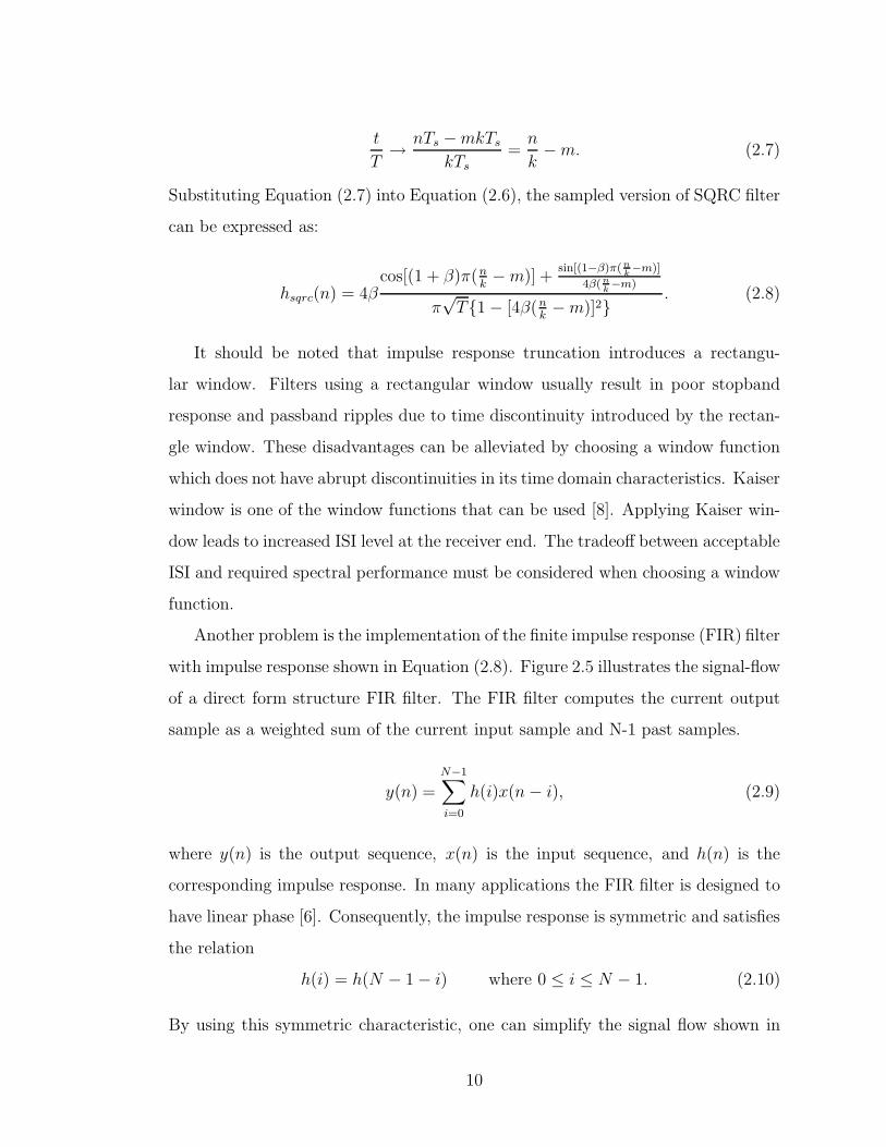
Another problem is the implementation of the finite impulse response (FIR) filter
with impulse response shown in Equation (2.8). Figure 2.5 illustrates the signal-flow
of a direct form structure FIR filter. The FIR filter computes the current output
sample as a weighted sum of the current input sample and N-1 past samples.
y(n) =N−1∑
i=0
h(i)x(n − i), (2.9)
where y(n) is the output sequence, x(n) is the input sequence, and h(n) is the
corresponding impulse response. In many applications the FIR filter is designed to
have linear phase [6]. Consequently, the impulse response is symmetric and satisfies
the relation
h(i) = h(N − 1 − i) where 0 ≤ i ≤ N − 1. (2.10)
By using this symmetric characteristic, one can simplify the signal flow shown in
10
)(nx
)(ny
)0(h )1(h
1z
)1(Nh...
)2(Nh
1z
1z
Figure 2.5 Signal flow graph of the direct form structure FIRfilter.
Figure 2.5.
The pulse shaping filter in a quadrature digital modulator can also be an FIR
filter with symmetric impulse response. From the theoretical point of view, the in-
put data sequences are upsampled by k before being processed by the pulse shaping
filters. The upsampled time series contains samples of the original inputs separated
by k − 1 zero valued samples. Figure 2.6 shows an example that the input data
sequence is upsampled by 4. This zero packed data sequence is then processed
by the SQRC filter. The SQRC filter actually limits the bandwidth to the band
of interest and computes output samples at an increased rate (k-to-1) relative to
input rate, replacing the zero packed values with the interpolated values. Figure
2.7 shows the output sequence when the upsampled data sequence shown in Figure
2.6 has been processed by a SQRC filter, where the filter length is 8 symbols (4
samples per symbol) and the roll-off factor is 0.22.
2.3 Interpolation filter
Interpolation filters in a modulator are used to raise the sampling rate to allow
the translation of the input signal spectrum to an intermediate frequency in the
digital domain. Two interpolation filter structures are considered here, cascaded
integrator comb (CIC) filter and half-band FIR filter. Both of these two structures
are hardware-efficient.
• Cascaded integrator comb (CIC) filter
A CIC filter consists of an integrator section operating at the high sampling rate
and a comb section operating at the low sampling rate [9]. From the theoretical
11

0 2 4 6 8 10 12 14 16−1.5
−1
−0.5
0
0.5
1
1.5
Time
Am
plitu
de
Figure 2.6 An example of 1-to-4 upsampling. “x” shows theinput binary data and “o” shows the output after1-to-4 upsampling.
0 5 10 15 20−1.5
−1
−0.5
0
0.5
1
1.5
Time
Am
plitu
de
Figure 2.7 Output sequence of a SQRC filter. “x” shows the in-put binary data and “o” shows the output sequence.
12

point of view, the CIC filter can either increase or decrease the sampling rate at
the output relative to the input, depending on the filter architecture.
Figure 2.8 shows the basic structure of the CIC interpolation filter. The comb
section operates at a low sampling rate, fs/R, where R is the integer rate change
factor. This section consists of N comb stages with a differential delay of M samples
per stage. The differential delay factor, which is usually 1 or 2 in a practical system,
is a filter design parameter used to control the filter’s frequency response. The
integrator section of the CIC filters consists of N ideal integrator stages operating
at the high sampling rate, fs. A rate change switch between two sections can cause
a rate increase by a factor of R by inserting R − 1 zero valued samples between
consecutive samples of the comb section output.
The system function for the composite CIC filter referenced to the high sampling
rate, fs, is
HCIC(z) =(1 − z−RM )N
(1 − z−1)N=
(
RM−1∑
k=0
z−k
)N
. (2.11)
The frequency response of CIC filter evaluated at z = e(2πf/R) is:
HCIC(f) =
[
sin(πMf)
sin(πf/R)
]N
, (2.12)
where f is the frequency relative to the low sampling rate fs/R.
CIC filter is chosen as one of the possible interpolation structures because it is
Mz
...
1z
...
Comb Section Integrator Section
Stage 1 ... Stage N Stage N+1 ... Stage 2N
Rf s / Rf s / sf sf
-1 -1
1z
Mz
Figure 2.8 Block diagram of the CIC interpolation filter.
13
very hardware efficient. The advantages of CIC filter are: (1) no multipliers are
required; (2) no storage is required for filter coefficients; (3) intermediate storage
is reduced compared to the equivalent implementation using cascaded uniform FIR
filters; and (4) the same filter design can be easily extended to a wide range of rate
change factors.
For the CIC interpolation filter design, the minimum register width must be
determined. Rounding can not be used because the small error in the integrator
stages can cause the variance of the error to grow without bound and result in an
unstable filter [9].
The minimum register width for jth filter stage, Wj , is determined by [9].
Wj = ⌈Bin + log2 Gj⌉ for j = 1, 2, ..., 2N, (2.13)
where Bin is the input register width, Gj is the maximum register growth up to
jth stage, and ⌈⌉ represents for ceiling function. Gj can be calculated according to
Equation (2.14).
Gj =
2j if j = 1, 2, ..., N,
22N−j (RM)j−N
Rif j = N + 1, ..., 2N.
(2.14)
There is a special case for Equation (2.13). When M = 1, the equation used to
calculate the minimum register width for Nth stage is expressed as:
WN = Bin + N − 1 if M = 1. (2.15)
• Half-band filter
Half-band filters are widely used in multirate signal processing applications when
interpolating/decimating by a factor of two. A half-band low pass filter has a pass
band bandwidth between ±14
sampling rate for a two-sided bandwidth equal to half
the sampling rate [10]. The impulse response of an ideal noncasual discrete filter
14

0 2 4 6 8 10 12 14 16 18 20−0.2
0
0.2
0.4
0.6
0 0.05 0.1 0.15 0.2 0.25 0.3 0.35 0.4 0.45 0.5−50
−40
−30
−20
−10
0
n
Am
plitu
de
Frequency normalized to sampling frequency
Am
plitu
de
(dB
)
h(n)
H(f)
Figure 2.9 Impulse response and frequency response of a halfband FIR filter with the length of 21.
can be shown as:
hhb(n) =1
2· sin(nπ/2)
nπ/2. (2.16)
The impulse response and the corresponding frequency response of a casual half-
band filter with the length of 21 are shown in Figure 2.9.
The impulse response of the half-band filter are all zero at the even index offsets
from the center point of the filter. The coefficients with odd index offsets are
symmetric about the filter center point. These two properties permit a half-band
filter with the length of 2N + 1 to be implemented with only N2
multiplications per
output sample. This structure is very efficient for upsampling applications. The
limitation for this filter is that the interpolation ratio can only be two. If several
half-band filters are connected serially, the interpolation ratio can be expanded to
the power of two.
15
I
Q
I-value
Q-value
Figure 2.10 I − Q format.
2.4 Modulation
To transmit a signal over the air, a carrier is modulated with the information to
be transmitted. This process usually involves modulating the amplitude, frequency
and/or phase of the carrier. A simple way to view the amplitude and phase is with
polar diagram. The carrier becomes a frequency and phase reference and the signal
is interpreted relative to the carrier. The signal can be expressed in polar form as
a magnitude and a phase.
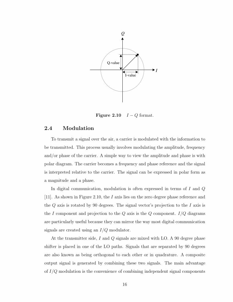
In digital communication, modulation is often expressed in terms of I and Q
[11]. As shown in Figure 2.10, the I axis lies on the zero degree phase reference and
the Q axis is rotated by 90 degrees. The signal vector’s projection to the I axis is
the I component and projection to the Q axis is the Q component. I/Q diagrams
are particularly useful because they can mirror the way most digital communication
signals are created using an I/Q modulator.
At the transmitter side, I and Q signals are mixed with LO. A 90 degree phase
shifter is placed in one of the LO paths. Signals that are separated by 90 degrees
are also known as being orthogonal to each other or in quadrature. A composite
output signal is generated by combining these two signals. The main advantage
of I/Q modulation is the convenience of combining independent signal components
16

into a composite signal and later splitting the signal into its independent component
parts.
At the receiver side, the composite signal with magnitude and phase informa-
tion is mixed with the LO signal at the carrier frequency in two forms. One is at
an arbitrary zero phase and another one has a 90 degree phase shift. The compos-
ite input signal is thus broken into an in-phase component, I, and a quadrature
component Q. These two components are independent and orthogonal.
Quadrature modulation can be accomplished with quadrature modulators. Most
quadrature modulators map the data to a number of discrete points on the I/Q
plane. These are known as constellation points. As the signal moves from one
points to another, simultaneous amplitude and phase modulation results.
• QPSK modulation
Quadrature Phase Shift Keying (QPSK) is a common type of phase modulation,
which is widely used in applications including CDMA cellular systems, wireless local
loop and DVB-S (Digital Video Broadcasting - Satellite). Quadrature means that
the signal shifts between phase states which are separated by 90 degrees. The
equation describing QPSK is:
s(t) = u(t) cos(ωct + θm), (2.17)
where θm ∈ {π4,−π
4, 3π
4,−3π
4} and u(t) is a real value pulse. The constellation
diagram for QPSK is shown in Figure 2.11. The signal shifts in increments of 90
degrees from 45 to 135, -45 or -135 degrees. These points are chosen as they can be
easily implemented using I/Q modulator. The symbol rate is half of the bit rate.
• QAM modulation
Another member of quadrature digital modulation family is Quadrature Ampli-
tude Modulation (QAM). QAM is used in applications including microwave digital
radio, DVB-C (Digital Video Broadcasting - Cable) and modems. The equation
describing QAM is:
s(t) = Vmu(t) cos(ωt + θm), (2.18)
17
I
Q
Figure 2.11 QPSK constellation.
where θm represents possible phase values, Vm represents possible amplitude values
and u(t) is a real value pulse.
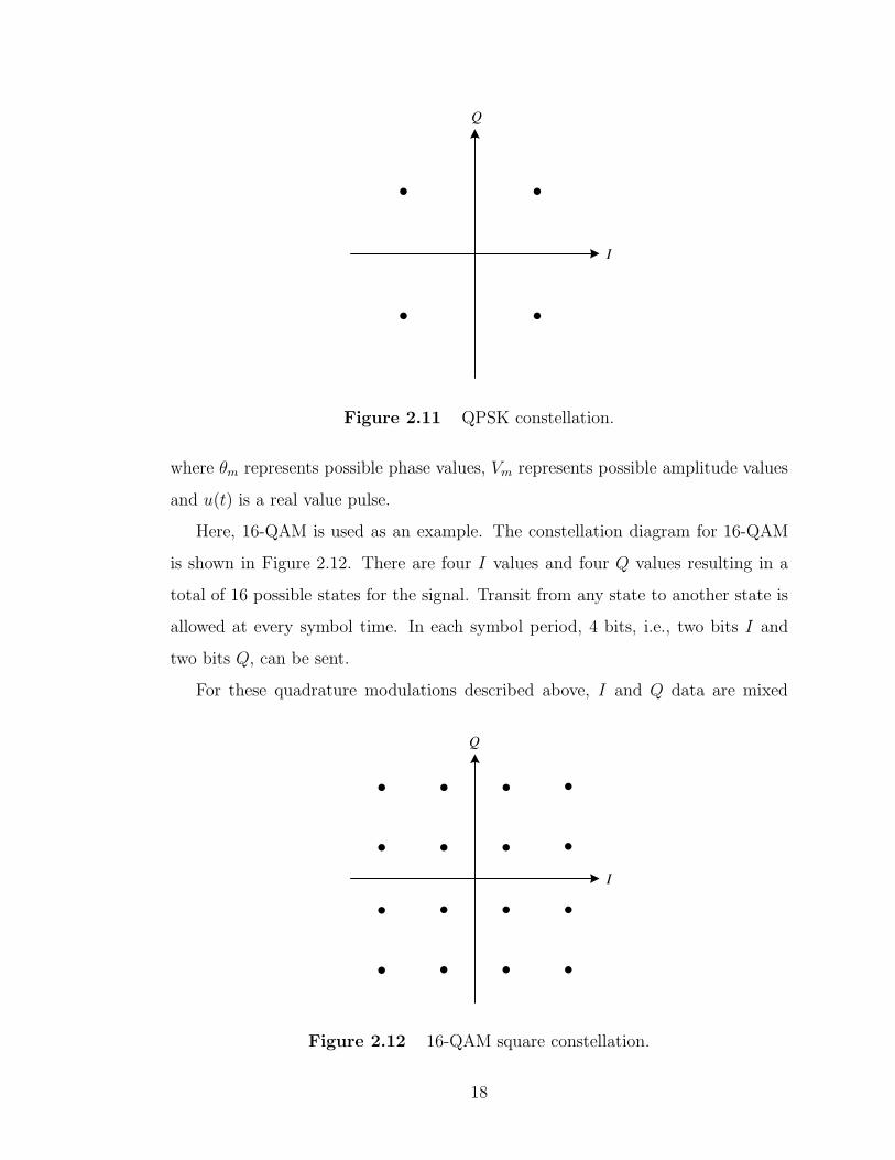
Here, 16-QAM is used as an example. The constellation diagram for 16-QAM
is shown in Figure 2.12. There are four I values and four Q values resulting in a
total of 16 possible states for the signal. Transit from any state to another state is
allowed at every symbol time. In each symbol period, 4 bits, i.e., two bits I and
two bits Q, can be sent.
For these quadrature modulations described above, I and Q data are mixed
I
Q
Figure 2.12 16-QAM square constellation.
18

together in a modulator after the pulse shaping and interpolation stages. The
whole modulation process can be described as:
y(t) = I(t) cos(ωct) − Q(t) sin(ωct). (2.19)
The carrier frequency is decided by programming the QDDS circuit with an appro-
priate tuning word. The digital sine and cosine data is multiplied by the Q and
I data respectively to create the quadrature components of the original data up-
converted to the carrier frequency. The quadrature components are then digitally
summed and passed on to the following stages. The key point is that the modu-
lation is done totally digital, which eliminates the phase and gain imbalance and
crosstalk issues typically associated with analog modulators [2].
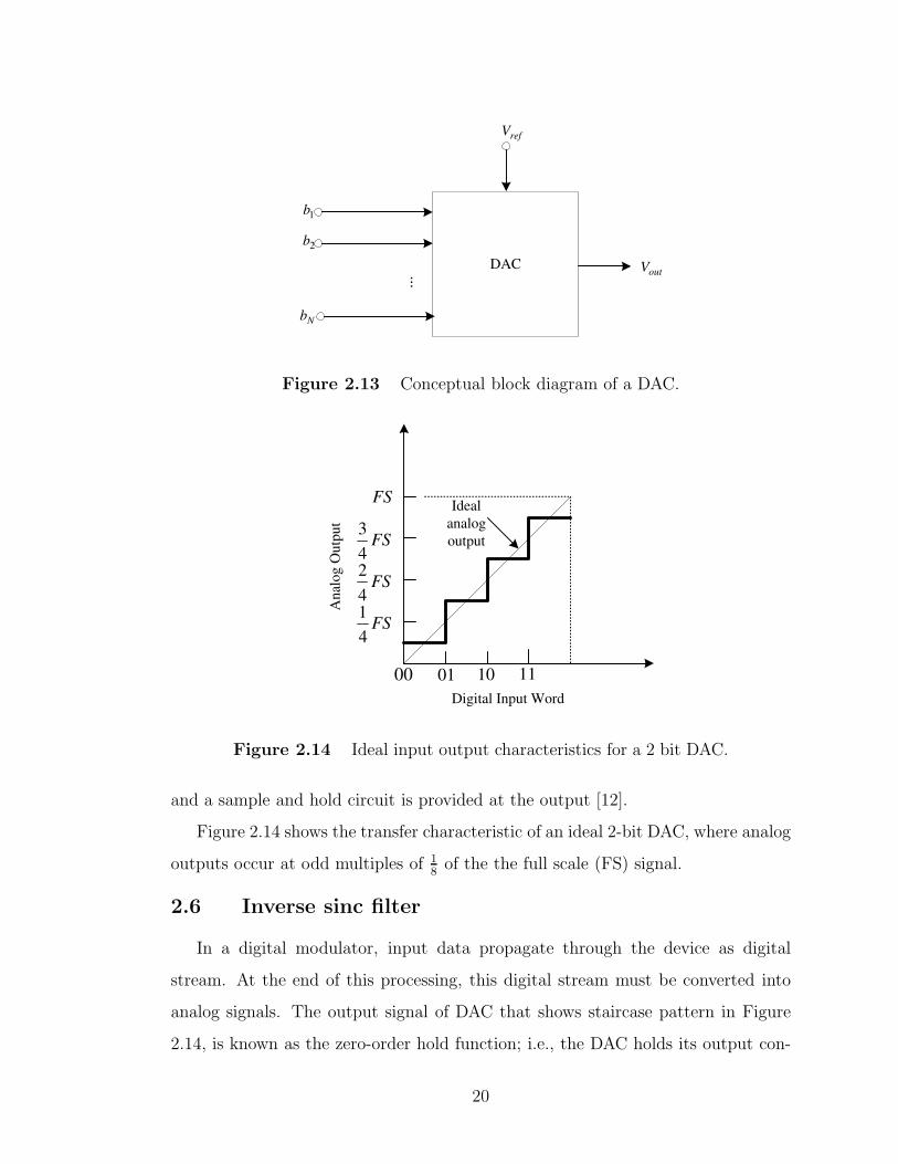
2.5 Digital to analog converter (DAC)
At the end of digital modulator, a DAC is needed to convert digital signals into
analog signals. There are several advantages with a DAC circuit on-chip. One
advantage is that the power consumption can be reduced compared with the design
which needs to drive an off-chip DAC. Another advantage is that it can avoid delays
and line loading caused by interchip connections.
Figure 2.13 shows the conceptual block diagram of the DAC. The inputs of the
DAC consists of a digital word of N bits and a reference voltage, Vref . The voltage
output, Vout, can be expressed as:
Vout = KVrefD, (2.20)
where K is a scaling factor and the digital word D is given as:
D = b12−1 + b22
−2 + b32−3 + + bN2−N , (2.21)
where bi is the ith bit coefficient. It is preferred that the digital word is syn-
chronously clocked. In this case, latches can be used to hold the word for conversion
19
DAC
1b
...
refV
outV
2b
Nb
Figure 2.13 Conceptual block diagram of a DAC.
01 10 1100
FS
FS4
1
FS4
2
FS4
3
Digital Input Word
Anal
og O
utp
ut
Ideal
analog
output
Figure 2.14 Ideal input output characteristics for a 2 bit DAC.
and a sample and hold circuit is provided at the output [12].
Figure 2.14 shows the transfer characteristic of an ideal 2-bit DAC, where analog
outputs occur at odd multiples of 18
of the the full scale (FS) signal.
2.6 Inverse sinc filter
In a digital modulator, input data propagate through the device as digital
stream. At the end of this processing, this digital stream must be converted into
analog signals. The output signal of DAC that shows staircase pattern in Figure
2.14, is known as the zero-order hold function; i.e., the DAC holds its output con-
20

stant for the entire sampling period. The spectrum of zero-order hold function is a
sinc envelope. The frequency response of the zero-order hold of the DAC is shown
in Equation (2.22) [13].
Hzo(f) =sin(πf/fs)
πfe−jπf/fs, (2.22)
where fs is sampling frequency.
The series of digital words presented at the input of the DAC represent the
desired transmitting signal. Due to the zero-order hold effect of the DAC, the
output spectrum of the output signal is the product of the sinc envelope and Fourier
transform of the desired output signal. Thus, there is an intrinsic sinc distortion in
the output spectrum.
If the desired output signal spectrum has the flat top amplitude, the output
spectrum from a real world DAC is illustrated in Figure 2.15. The amplitude of the
output signal and its images follows a sinc response. The amplitude roll off due to
this envelop in a system is 3.92 dB in the first Nyquist zone. Since the sinc response
is deterministic and predictable, it is possible to predistort the input data stream
in a manner that compensates for the sinc envelop distortion. An inverse sinc filter
(ISF) can be used in front of DAC which will pre-compensate for the roll off and
maintain flat output amplitude over the bandwidth of the first Nyquist zone. The
amplitude response of an ideal inverse sinc filter and its impact on the whole system
is shown in Figure 2.16. The frequency response of this FIR filter is the inverse sinc
function. Thus, the data sent through this filter is altered to correct for the sinc
envelop distortion. This inverse sinc filter can also be bypassed depending upon
applications.
The desired amplitude response of the inverse sinc filter can be described as:
Hd(f) =πf/fs
sin(πf/fs)where 0 ≤ f ≤ fs/2. (2.23)
With this desired response, a digital filter can be designed using the minimum mean
21

0 0.5 1 1.5 2 2.5 3 3.5−40
−35
−30
−25
−20
−15
−10
−5
0fundamental
1st image
2nd image3rd image
sinc envelope
Frequency normalized to sampling frequency
Am
plitu
de
(dB
)
Figure 2.15 Output spectrum of a real world DAC.
0 0.05 0.1 0.15 0.2 0.25 0.3 0.35 0.4 0.45 0.5−4
−3
−2
−1
0
1
2
3
4
Frequency normalized to sampling frequency
Am
plitu
de
resp
onse
(dB
)
ISFSincSystem
Figure 2.16 Amplitude response of the ideal inverse sinc filter.
22
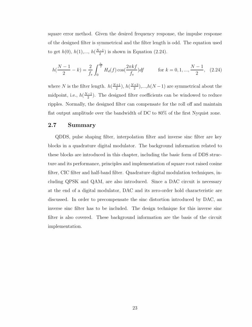
square error method. Given the desired frequency response, the impulse response
of the designed filter is symmetrical and the filter length is odd. The equation used
to get h(0), h(1),..., h(N−12
) is shown in Equation (2.24).
h(N − 1
2− k) =
2
fs
∫fs2
0
Hd(f) cos(2πkf
fs)df for k = 0, 1, ...,
N − 1
2, (2.24)
where N is the filter length. h(N+12
), h(N+32
),...,h(N −1) are symmetrical about the
midpoint, i.e., h(N−12
). The designed filter coefficients can be windowed to reduce
ripples. Normally, the designed filter can compensate for the roll off and maintain
flat output amplitude over the bandwidth of DC to 80% of the first Nyquist zone.
2.7 Summary
QDDS, pulse shaping filter, interpolation filter and inverse sinc filter are key
blocks in a quadrature digital modulator. The background information related to
these blocks are introduced in this chapter, including the basic form of DDS struc-
ture and its performance, principles and implementation of square root raised cosine
filter, CIC filter and half-band filter. Quadrature digital modulation techniques, in-
cluding QPSK and QAM, are also introduced. Since a DAC circuit is necessary
at the end of a digital modulator, DAC and its zero-order hold characteristic are
discussed. In order to precompensate the sinc distortion introduced by DAC, an
inverse sinc filter has to be included. The design technique for this inverse sinc
filter is also covered. These background information are the basis of the circuit
implementation.
23
Chapter 3
Integrated Circuit Design Flow
The semiconductor industry has evolved from the first integrated circuit of early
1960s and matured rapidly since then. Early small-scale integrated circuits con-
tained only a few logic gates. It is well known as Moore’s law that the number of
transistors on an integrated circuit for minimum component cost doubles every 18
months [14]. Current very large scale integration (VLSI) ICs can combine millions
of gates on a single device.
Accompanied with the fast advancement of IC fabrication processing technology,
IC designers face many design challenges. ITRS 2005 report listed a number of the
challenges [3] in which two are related to design technology.
1. Design productivity, which is closely linked to system and design process
complexity, and of course affecting design cost, is the most massive and critical
challenge. Issues related to it include high level of abstraction, system integration
and analog circuit synthesis, etc.
2. Manufacturability, that is, the ability to produce a chip in large quantities
at acceptable cost and according to an economically feasible schedule, has been
affecting the industry primarily due to lithography hardware limitations but will
become a major crisis in the long term as variability in its multiple forms invades all
aspects of a design. Design issues include device parameter variability, mixed-signal
test and quality models, etc.
A good design flow can increase both design productivity and manufacturability.
Since the IC design in this thesis is totally digital, the digital IC design flow chosen
is described as follows.
24
3.1 Digital IC design flow
The design flow for creating VLSI digital circuits consists of a sequence of steps.
Each step in the design flow either creates a database supporting the design flow,
or verifies that the design meets specific requirements. Generally speaking, these
steps can be separated into front-end design flow and back-end design flow. The
front-end design flow focuses on the steps of preparing a gate-level netlist to be
used in physical design of the chip. The back-end design flow focuses on steps of
the physical design and ends up with a mask layout for fabrication. The main
design flow described in this chapter is similar to the design flow provided by CMC
microsystems [15]. Some modifications are made to make the whole design flow
more flexible and more suitable for large designs.
3.1.1 Front-end design flow
Figure 3.1 shows the front-end design flow which includes the design steps before
the physical layout of an IC design. The first step is register transfer level (RTL)
coding which describes the functionality of a design. The RTL coding can be written
in Verilog or VHDL. Verilog is chosen as the RTL coding language in this thesis.
The second step is to verify the functionality of the RTL code using an hard-
ware descriptive language (HDL) simulator. A corresponding testbench must be
provided for verification. The simulator used in this step is NC-Sim. The design
and the testbench files, both in Verilog, must be compiled first. The command used
to compile Verilog files is ncvlog. It performs syntactic and semantic checking on
the Verilog design units. If no errors are found, compilation produces an internal
representation for each HDL design unit in the source files. Before one can run
simulation, the design must be ‘elaborated’ to construct a design hierarchy based
on the instantiation and configuration information in the design, to establish sig-
nal connectivity, and to compute initial values for all objects in the design. The
command used for elaborating the design is called ncelab. The elaborated design
hierarchy is stored as a simulation ‘snapshot’, which is the representation of the de-
sign that the simulator uses to run simulations. The snapshot is stored in a library
25

Verify RTL code
Constrain the design
Generate gate-level netlist
Verify gate-level netlist
Insert scan chain and
generate test pattern
Add I/O cells
Output constraints files
Write RTL code
Cadence-NC-Sim
Synopsys-
Design Compiler
Cadence-NC-Sim
Mentor Graphics-
DFTAdvisor and Fastscan
Synopsys-
Design Compiler
Text editor
Tools
Testbench
Test patterns
Fault simultion Cadence-NC-Sim
Procedure Intermediate input
and output
Figure 3.1 Block diagram of the front-end design flow.
26
database file along with the other intermediate objects generated by the compiler
and elaborator. After compilation and elaboration, one can invoke the simulator,
NC-Sim, to verify Verilog design.
The design flow provided by CMC microsystems suggests that users use NC-Sim
in graphical user interface (GUI) mode. However, it is more convenient to verify the
functionality in batch mode for large designs so that designers can observe inputs,
outputs and internal nodes over a long period of time. Appendix A.1 shows one
script example for invoking the simulator in batch mode.
After functional verification, the design is ready for synthesis. The logic syn-
thesizer used is Synopsys Design Compiler. In order to synthesize the design, the
same RTL code has to be analyzed and elaborated again. Similar with NC-Sim, the
analysis step checks the syntax and semantics of Verilog files. The elaborate com-
mand replaces Verilog operators with equivalent combinational logic and determines
correct bus sizes.
The next step is to set constraints for the design. The constraints here refer
to defining the clock, specifying I/O cells, defining output load, etc. With these
pre-set constraints, the design compiler can automatically create a gate-level netlist
for a targeted processing technology. Synopsys Design Compiler can also report the
timing, area and power consumption of the design.
The logic synthesis procedure described in the CMC microsystems’ design flow
are performed in GUI mode. Due to the fact that a design will be synthesized for
several times with different constraints, an efficient way to use the logic synthesizer
is to perform the synthesis in batch mode instead of GUI mode. Appendix A.2
shows one example script for using the logic synthesizer in batch mode. It should
be noted that this example script contains basic synthesis steps only. One needs to
modify it to meet different synthesis requirements.
To ensure the resulted gate-level netlist is correct, one needs to verify the func-
tionality of the gate-level netlist following the same procedure as RTL code veri-
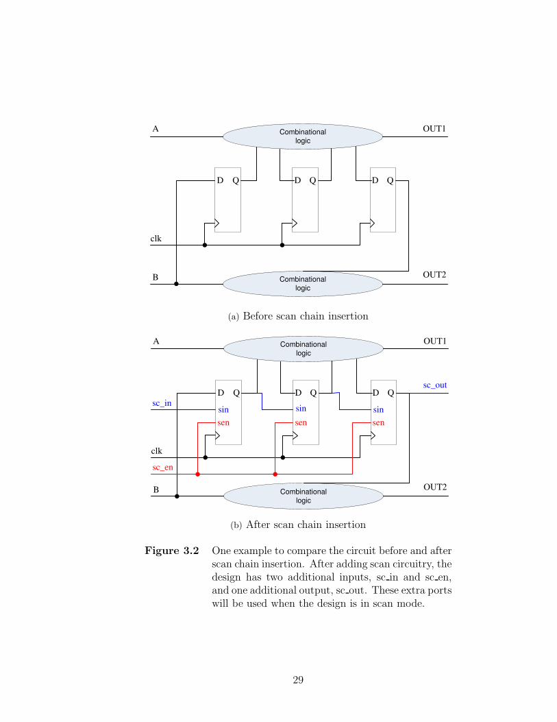
fication. With the verified gate-level netlist, one can insert the scan chain using
Mentor Graphics DFTAdvisor. The purpose of inserting scan chain is to improve
27

the testability of the fabricated chip for physical defects. This step involves re-
placing sequential elements with scannable sequential elements and then stitching
the scan cells together into scan registers, or scan chains. Figure 3.2 shows one
example before and after scan chain insertion [16]. Testing engineers can then use
these serially-connected scan cells to shift data in and out when the design is in
scan mode.
The next step after scan chain insertion is automatic test pattern generation
(ATPG). Test patterns generated in this step are sets of 1s and 0s placed on primary
input pins during manufacturing test process to determine if the chip is functioning
properly. When the test pattern is applied, the automatic test equipment (ATE)
determines if the circuit is free from manufacturing defects by comparing the fault-
free output which is also contained in the test pattern with the actual output
measured by the ATE. The tool used in this step is Mentor Graphics Fastscan.
Both the DFTAdvisor and Fastscan are used under batch mode. The generated
test patterns can be verified in NC-Sim.
After scan chain insertion, the gate-level netlist with scan chain is read back to
Synopsys Design Compiler to finalize the design by adding I/O cells and output
corresponding constraint files.
3.1.2 Back-end design
The back-end design flow, which consists of the design steps of physical layout, is
shown in Figure 3.3. The flow begins with virtual design procedure, which involves
I/O cells placement, power planning and trial placement and routing. During the
trial placement and routing of the virtual design procedure, cells are placed and
routed without consideration for timing. The next step is to use Cadence Physically
Knowledgeable Synthesis (PKS) to optimize the design with the consideration of
timing constraints and parasitic values. The design is optimized for three separate
times to account for parasitics that are obtained during place and route to attain
a high performance. It should be noted that all the optimizations in this step are
based on an ‘ideal’ clock.
28
clk
Combinational
logic
Combinational
logic
A
B
D Q D Q D Q
OUT1
OUT2
(a) Before scan chain insertion
clk
Combinational
logic
Combinational
logic
A
B
D Q D Q D Q
OUT1
OUT2
sc_en
sc_in
sc_out
sen sen sen
sin sin sin
(b) After scan chain insertion
Figure 3.2 One example to compare the circuit before and afterscan chain insertion. After adding scan circuitry, thedesign has two additional inputs, sc in and sc en,and one additional output, sc out. These extra portswill be used when the design is in scan mode.
29

Placement and optimization
Clock tree synthesis
Timing optimization
Routing
Static timing analysis
Tape out
Floorplan
Cadence-PKS
Cadence-Encounter
Tools
Post layout verification
(LVS, DRC)Cadence-Diva, Calibre
ProcedureIntermediate input
and output
Golden verilog netlist
Cadence-Encounter
Figure 3.3 Block diagram of the back-end design flow.
30
After the placement and optimization, clock tree synthesis can be performed.
Cadence PKS treats clock tree as an entire sub-circuit and adds buffers into the
tree during the clock tree synthesis process. With the physically inserted clock tree,
optimizations based on the real propagated clock can be performed.
The design is ready for the final route and optimization after the clock tree
insertion. With this step done, one needs to perform static timing analysis to make
sure the routed design meets the timing goal.
The final steps before tape out are mainly to verify the physical layout of the
design. These steps include layout versus schematic (LVS) verification and design
rule check (DRC). LVS is to verify that the physical layout contains the same
instances, nets and connectivity as the verified design netlist and DRC is to verify
that the physical layout meets the foundrys design rule.
It is a good practice to carry out all the steps involved in back-end design in
batch mode in stead of GUI mode. Appendix A.3 shows one script example for
timing optimization after clock tree insertion using Cadence PKS.
It should be noted that the design flows of front-end design and back-end design
shown in Figure 3.1 and Figure 3.3 assume that the design requirements can be
met at every stage. In practical design, there will be several changes in iterations
of the design or constraints at various design points until the design requirements
are met.
3.2 Summary
To tackle the challenges of integrated circuit design productivity and manufac-
turability, it is very important to choose the right design flow. The whole integrated
circuit design flow are generally split into front-end design flow and back-end de-
sign flow. Both of them are discussed step by step in this chapter. Compared with
CMC microsystems’ design flow, the design flow introduced here is more efficient
and flexible as a result of extensive use of scripts for batch mode processing. Some
simple scripts are also provided as examples.
31
Chapter 4
Circuit Design and Low Power Considerations
Low-power circuits can be achieved at different levels. At system level, dynamic
power management can be used to dynamically reconfiguring systems to provide the
requested services and performances with a minimum number of active components
or a minimum load on such components. At algorithm level, different algorithms
can be compared for their power consumptions to identify one with the lowest power
consumption. At circuit level, parallelization implementation, multiple supply volt-
ages, dynamic supply voltage scaling, retiming, etc., can be used to reduce power
consumption. At transistor level, variable threshold transistors, dynamic thresh-
old voltage scaling, input vector control, etc., can be used to reduce leakage power
which has become more and more important in nanometric technologies. Most of
the low-power techniques used in this thesis are at algorithm level. Some low-power
techniques at system level and circuit level are also used.
4.1 Quadrature digital modulator
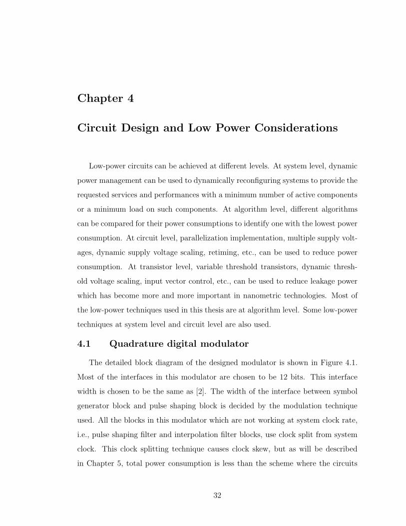
The detailed block diagram of the designed modulator is shown in Figure 4.1.
Most of the interfaces in this modulator are chosen to be 12 bits. This interface
width is chosen to be the same as [2]. The width of the interface between symbol
generator block and pulse shaping block is decided by the modulation technique
used. All the blocks in this modulator which are not working at system clock rate,
i.e., pulse shaping filter and interpolation filter blocks, use clock split from system
clock. This clock splitting technique causes clock skew, but as will be described
in Chapter 5, total power consumption is less than the scheme where the circuits
32
Symbol
Generator
I
Q
QDDS
Inverse
Sinc Filter
Mux
12
12
1212
12
12
12
12
12
12Interpolation
Filter
12
12Interpolation
Filter
Pulse
Shaping
Filter
Pulse
Shaping
Filter
Clock Circuit
DAC
Ref
clo
ckB
aseb
and d
ata
Figure 4.1 The detailed block diagram of the designed quadrature digital modulator.
33

Complementor sine ROM Complementor
MSB
2nd MSB
2
0
2
0
2/
02nd MSB MSB
2
aN
2aN 2aN 1dN dN
2/
Figure 4.2 ROM design using quarter-wave symmetry.
operate at the same high clock speed. The maximum system clock rate is targeted
at 150 MHz in this design, i.e., output bandwidth is from 0 to 75 MHz. This clock
speed is enough for most of the real applications because the highest intermediate
frequency is usually 70 MHz.
4.2 QDDS
4.2.1 ROM compression
In the conventional DDS design [17], a commonly used technique to design the
phase-to-amplitude converting ROM is illustrated in Figure 4.2. The ROM stores
only 0 to π2
of sine wave instead of 0 to 2π, i.e., it uses quarter-wave symmetry
to generate a full range sine wave. The most significant bit (MSB) determines the
sign of the output and second MSB determines whether the phase between 0 to π2
should be increasing or decreasing. The rest Na − 2 bits are used to address a sine
ROM.
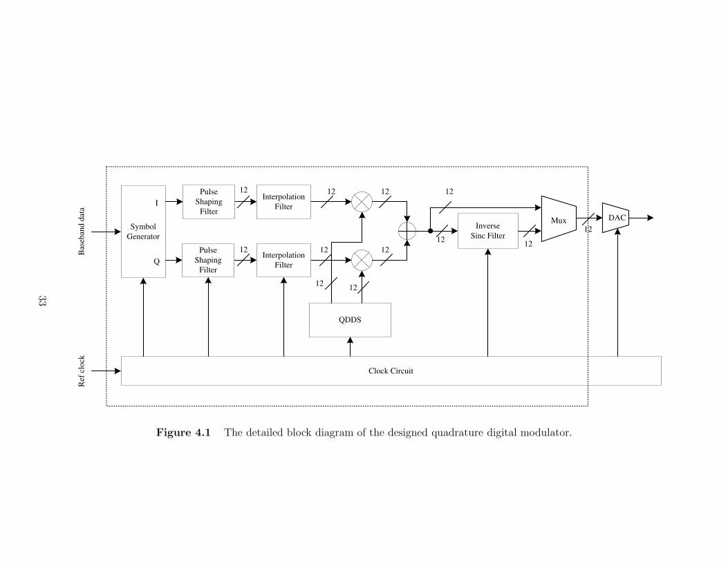
In this design, a 12
least significant bit (LSB) offset must be introduced in all
phase addresses. If the phase address, Na, is assumed to be 3 bits, Figure 4.3
shows the phase wheel comparison between no phase offset and 12-LSB phase offset.
Figure 4.4 shows error comparison between them. As one can see from Figure 4.4,
if quarter-wave ROM stores sin(0) and sin(π4), i.e., without phase offset, there are
some errors introduced because one’s complementor can’t map the phase values
without errors. If quarter-wave ROM stores sin(π8) and sin(3π
8), i.e., with 1
2-LSB
34
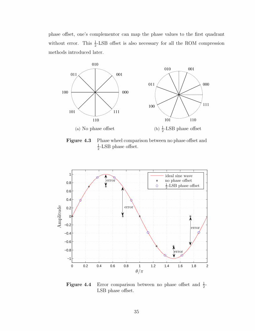
phase offset, one’s complementor can map the phase values to the first quadrant
without error. This 12-LSB offset is also necessary for all the ROM compression
methods introduced later.
000
001
010
011
100
101
110
111
(a) No phase offset
000
001010
011
100
101 110
111
(b) 12-LSB phase offset
Figure 4.3 Phase wheel comparison between no phase offset and12-LSB phase offset.
0 0.2 0.4 0.6 0.8 1 1.2 1.4 1.6 1.8 2
−1
−0.8
−0.6
−0.4
−0.2
0
0.2
0.4
0.6
0.8
1
θ/π
Am
plitu
de
ideal sine waveno phase offset1
2-LSB phase offset
error
error
error
error
Figure 4.4 Error comparison between no phase offset and 12-
LSB phase offset.
35

The conventional design only needs to store a quarter of the sine wave values
without introducing any errors. However, the ROM size is still too big considering
ROM is the most power hungry part in a DDS circuit [17]. One way to reduce the
ROM size is Suntherland algorithm [18]. In this algorithm, the phase address of
the quarter-wave, θ, is decomposed to three components; i.e., θ = α + β + γ.
sin(α + β + γ) = sin(α + β) cos(γ) + cos(α + β) sin(γ)
≈ sin(α + β) + cos(α) sin(γ), (4.1)
where α, β and γ are the MSBs, the middle bits, and the LSBs of the phase address,
respectively. The variables α and β form a ‘coarse’ ROM address and the variables
α and γ form a ‘fine’ ROM address. If the word lengths of α, β and γ are assumed to
be A, B and C, computer simulations are usually used to determine the optimum
partitioning of the ROM address. Assume the word length of the input phase
address is 12 bits and output sine samples are also 12 bits, i.e., the phase address
of the quarter-wave sine ROM is 10 bits and the output of quarter-wave sine ROM
is 11 bits, Table 4.1 shows partition simulation results. Given the tradeoff between
mean square error and ROM size, A = 4, B = 3 and C = 3 are optimum choices for
this scenario, where the output of the coarse ROM is 11 bits and the output of the
fine ROM is 5 bits. As one can see from this example, this method can compress
the ROM size. The compression ratio achieved here is 210×11
27×11+27
×5= 5.5.
Based on the Suntherland algorithm, the sine phase difference method was in-
troduced in [19] to reduce the size of coarse ROM. With the sine phase difference
method, the coarse ROM stores the sine phase difference instead of the real sine
values. The equation used to describe sine phase difference method is:
y(θ) = sin(θ) − 2θ
π. (4.2)
Since the maximum value of sine phase difference, y(θ), is less than 14, this method
can save 2 bits of word length of the data in the coarse ROM.
36

Table 4.1 Comparison between different A, B, C partitions.
error2 ROM size (bits)
A = 6, B = 3, C = 1 2.7675 × 10⁻¹⁰ 29 × 11 + 27 × 3 = 6016
A = 4, B = 3, C = 3 7.4979 × 10⁻⁸ 27 × 11 + 27 × 5 = 2048
A = 3, B = 5, C = 2 7.5748 × 10⁻⁸ 28 × 11 + 25 × 4 = 2944
A = 3, B = 4, C = 3 3.0273 × 10⁻⁷ 27 × 11 + 26 × 5 = 1728
A = 3, B = 3, C = 4 1.1813 × 10⁻⁶ 26 × 11 + 27 × 6 = 1472
A = 3, B = 2, C = 5 4.4364 × 10⁻⁶ 25 × 11 + 28 × 7 = 2144
A = 2, B = 5, C = 3 1.1784 × 10⁻⁶ 27 × 11 + 25 × 5 = 1568
A = 2, B = 4, C = 4 4.6640 × 10⁻⁶ 26 × 11 + 26 × 6 = 1088
A = 2, B = 3, C = 5 1.8129 × 10⁻⁵ 25 × 11 + 27 × 7 = 1248
A = 1, B = 5, C = 4 1.7011 × 10⁻⁵ 26 × 11 + 25 × 6 = 896
A = 1, B = 3, C = 6 2.5962 × 10⁻⁴ 24 × 11 + 27 × 8 = 1200
Double trigonometric approximation method is revised to reduce the coarse
ROM size. The coarse ROM stores the errors between the sine phase difference and
a triangle waveform. The double trigonometric line, d(θ), can be expressed as:
d(θ) =
θ2π
if 0 ≤ θ < π4,
14− θ
2πif π
4≤ θ ≤ π
2.
(4.3)
Because the maximum error of the double trigonometric approximation is less than
18, this method can save 3 bits of word length of the data in the coarse ROM. The
data for 0 ≤ θ < π4
are generated by shifting right the phase, 2θπ
, by 2 bits. The
data for π4≤ θ ≤ π
2are symmetric and can be accomplished by a complementor.
Quad line approximation (QLA) method [17] can further compress coarse ROM
size. Similar to the double trigonometric approximation, the coarse ROM only
stores the errors between the sine phase difference and the quad line waveform.
37
The quad line waveform, q(θ), is expressed as follows:
q(θ) =
θπ
if 0 ≤ θ < π8,
116
+ θ2π
if π8≤ θ < π
4,
116
− θ2π
+ 14
if π4≤ θ < 3π
8,
12− θ
πif 3π
8≤ θ ≤ π
2.
(4.4)
The data for 0 ≤ θ < π8
are generated by shifting right the phase, 2θπ
, by 1 bits.
The data for π8≤ θ < π
4are generated by shifting right the phase by 2 bits and
by changing the first and second MSBs of the phase to “10”. These data are
implemented with a MUX. The data for π4≤ θ ≤ π
2are symmetric and can be
accomplished by a complementor.
Since the maximum value of QLA errors is less than 116
, the QLA method can
save 4 bits of word length of the data in the coarse ROM. The waveforms of sine-
phase difference, double trigonometric approximation, QLA are shown in Figure
4.5. The errors of double trigonometric approximation and QLA methods are also
shown in the same figure.
Table 4.2 compares different implementation choices for the coarse ROM. As the
QLA method can save 4 bits of the word length for the coarse ROM with simple
additional circuits, this method is chosen as the DDS implementation structure in
the modulator. For a DDS ROM with 12 bits phase address and 12 bits output
sine samples, the conventional design needs a 210 × 11 bits ROM. Based on the
Suntherland algorithm and the simulation results shown in Table 4.1, the input
phase address can first be decomposed to α, β and γ with lengths of 4, 3 and 3
respectively. Together with the QLA method, the ROM can be implemented with
a 27 × 7 bits coarse ROM and a 27 × 5 bits fine ROM. The total compression ratio
achieved is 210×11
27×7+27
×5= 7.33. The implementation block diagram of such a sine-to-
amplitude converting ROM using QLA method is shown in Figure 4.6. Similar to
the conventional design shown in Figure 4.2, the second MSB determines whether
the amplitude is increasing or decreasing. {α, β} is used to address the coarse sine
38
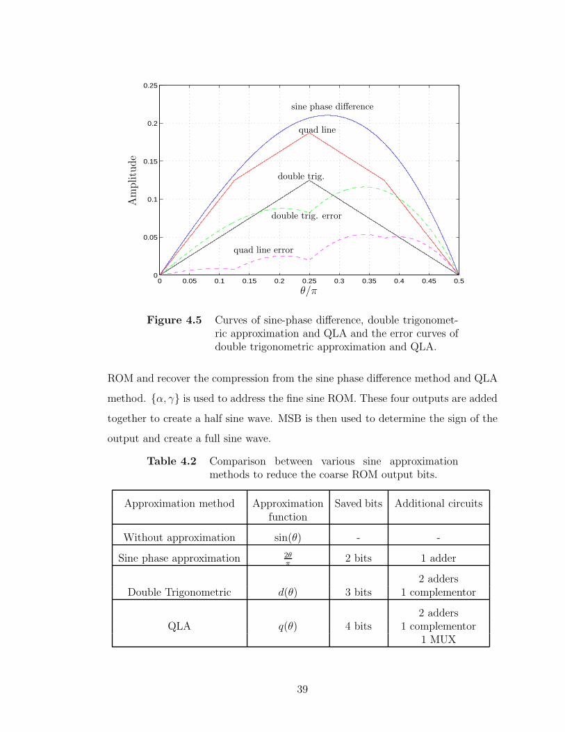
0 0.05 0.1 0.15 0.2 0.25 0.3 0.35 0.4 0.45 0.50
0.05
0.1
0.15
0.2
0.25
θ/π
Am
plitu
de
sine phase difference
quad line
double trig.
double trig. error
quad line error
Figure 4.5 Curves of sine-phase difference, double trigonomet-ric approximation and QLA and the error curves ofdouble trigonometric approximation and QLA.
ROM and recover the compression from the sine phase difference method and QLA
method. {α, γ} is used to address the fine sine ROM. These four outputs are added
together to create a half sine wave. MSB is then used to determine the sign of the
output and create a full sine wave.
Table 4.2 Comparison between various sine approximationmethods to reduce the coarse ROM output bits.
Approximation method Approximation Saved bits Additional circuitsfunction
Without approximation sin(θ) - -
Sine phase approximation 2θπ
2 bits 1 adder
2 addersDouble Trigonometric d(θ) 3 bits 1 complementor
2 addersQLA q(θ) 4 bits 1 complementor
1 MUX
39

Complementor
12
102
2nd MSB
MSB
Adders
Coarse
Sine
ROM
Complementor
Complementor
Mux
Phase
},{},{
12
11
7
7
0 0 1 0
)3(
)2(
}),0:2({
}),0:1({
7
Sine
3,3,4 CBA
Fine
Sine
ROM
5
},{
},,{
)0:4()0:6()4:10()2:8(
Figure 4.6 Sine phase to amplitude converter using QLAmethod.
An example is used here to demonstrate how the sine-to-amplitude converting
ROM shown in Figure 4.6 works. If the 12-bit input is assumed to be 0B000110001101,
the corresponding phase is 2π×397212 + 1
2× 2π
212 and the ideal output is 0.572669.
Since the second MSB is zero, {α, β, γ} is the least significant 10 bits of the in-
put and α, β, γ are 0B0110, 0B001, 0B101, respectively. Binary word {α, β} is
used to address the coarse sine ROM and the output is 0B0110010. Binary word
40
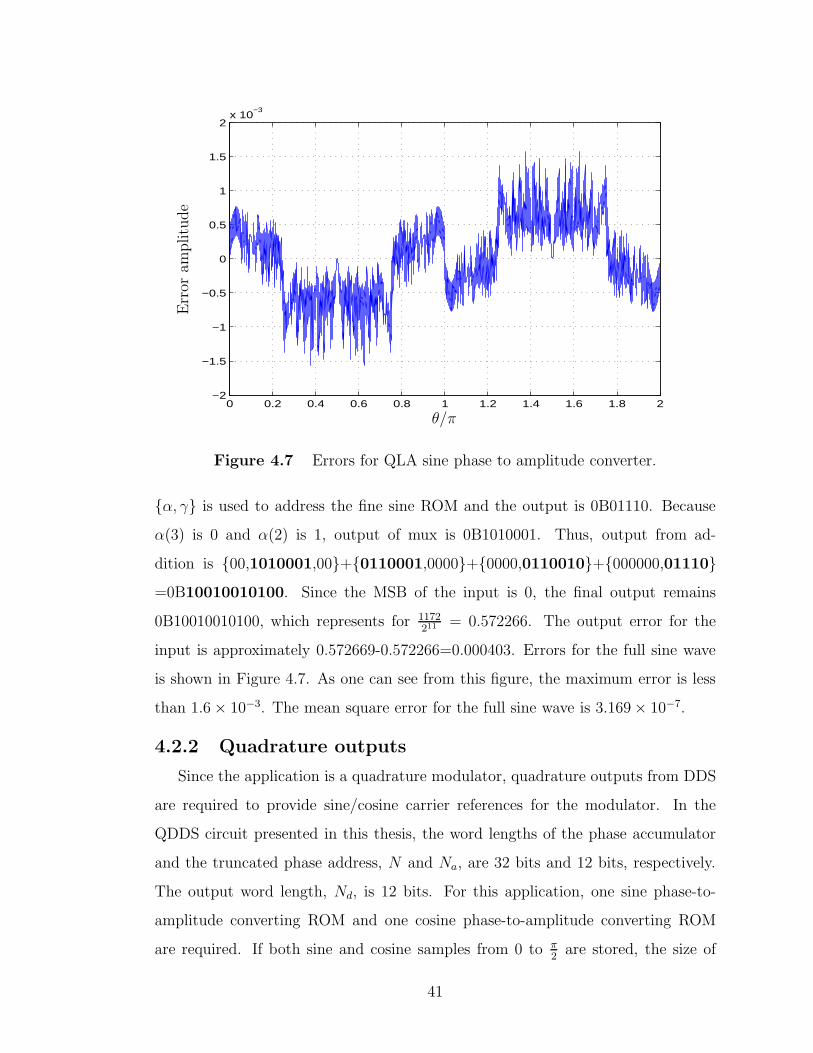
0 0.2 0.4 0.6 0.8 1 1.2 1.4 1.6 1.8 2−2
−1.5
−1
−0.5
0
0.5
1
1.5
2x 10
−3
θ/π
Err
oram
plitu
de
Figure 4.7 Errors for QLA sine phase to amplitude converter.
{α, γ} is used to address the fine sine ROM and the output is 0B01110. Because
α(3) is 0 and α(2) is 1, output of mux is 0B1010001. Thus, output from ad-
dition is {00,1010001,00}+{0110001,0000}+{0000,0110010}+{000000,01110}=0B10010010100. Since the MSB of the input is 0, the final output remains
0B10010010100, which represents for 1172211 = 0.572266. The output error for the
input is approximately 0.572669-0.572266=0.000403. Errors for the full sine wave
is shown in Figure 4.7. As one can see from this figure, the maximum error is less
than 1.6 × 10⁻³. The mean square error for the full sine wave is 3.169 × 10⁻⁷.
4.2.2 Quadrature outputs
Since the application is a quadrature modulator, quadrature outputs from DDS
are required to provide sine/cosine carrier references for the modulator. In the
QDDS circuit presented in this thesis, the word lengths of the phase accumulator
and the truncated phase address, N and Na, are 32 bits and 12 bits, respectively.
The output word length, Nd, is 12 bits. For this application, one sine phase-to-
amplitude converting ROM and one cosine phase-to-amplitude converting ROM
are required. If both sine and cosine samples from 0 to π2
are stored, the size of
41
the ROM will be doubled. Since sine samples from 0 to π4
are the same as cosine
samples from π2
to π4
and sine samples from π4
to π2
are the same as cosine samples
from π4
to 0, only the sine and cosine samples from 0 to π4
need to be stored. The
third MSB and the second MSB are XORed to select the data between 0 to π4
sine
samples and 0 to π4
cosine samples. Because only 0 to π4
sine and cosine samples
are stored, the lowest 9 bits of the 12 bits phase address are actually needed for
the sine and cosine look up tables. This 9-bit phase is decomposed to α + β + γ
according to the Suntherland algorithm. Since the data stored in 0 to π4
sine ROM
and 0 to π4
cosine ROM are the same as a 0 to π2
sine ROM, the simulation data
shown in Table 4.1 is still applicable for determining the wordlength of α, β and
γ. The only difference is that the actual word length of α is A-1 now. Given the
relationship between mean square error and ROM size, the word lengths of α, β
and γ are chosen to be 3, 3 and 3, respectively. The coarse sine ROM and coarse
cosine ROM are then further compressed by the sine phase difference method and
QLA method. Since the phase of stored samples are from 0 to π4, only the two
expressions between 0 to π4
shown in Equation (4.4) are used. The data for the
phase between 0 to π8
are generated by shifting right the phase by 1 bit and the
data for the phase between π8
to π4
are generated by shifting right the phase by 2
bits and changing the highest two bits to “10”.
The block diagram of the proposed QDDS is shown in Figure 4.8. The sizes
for coarse sine ROM, fine sine ROM, coarse cosine ROM and fine cosine ROM
are 26 × 6, 26 × 5, 26 × 7 and 26 × 4 bits, respectively. Instead of designing four
ROMs with different sizes, the word lengths of the coarse sine ROM and fine cosine
ROM are increased by 1 bit. As a result, the two coarse ROMs are 26 × 7 bits
and the two fine ROMs are 26 × 5 bits. Compared with the conventional design
which needs two 210 × 11 bits ROM, the total ROM compression ratio achieved is
2×210×11
2×26×7+2×26
×5= 14.7.
As one can see in Figure 4.8, additional adders and muxes are needed to re-
construct the output sine and cosine waves. These extra hardware are worthwhile
considering the savings from the area and power. It should be noted that these
42
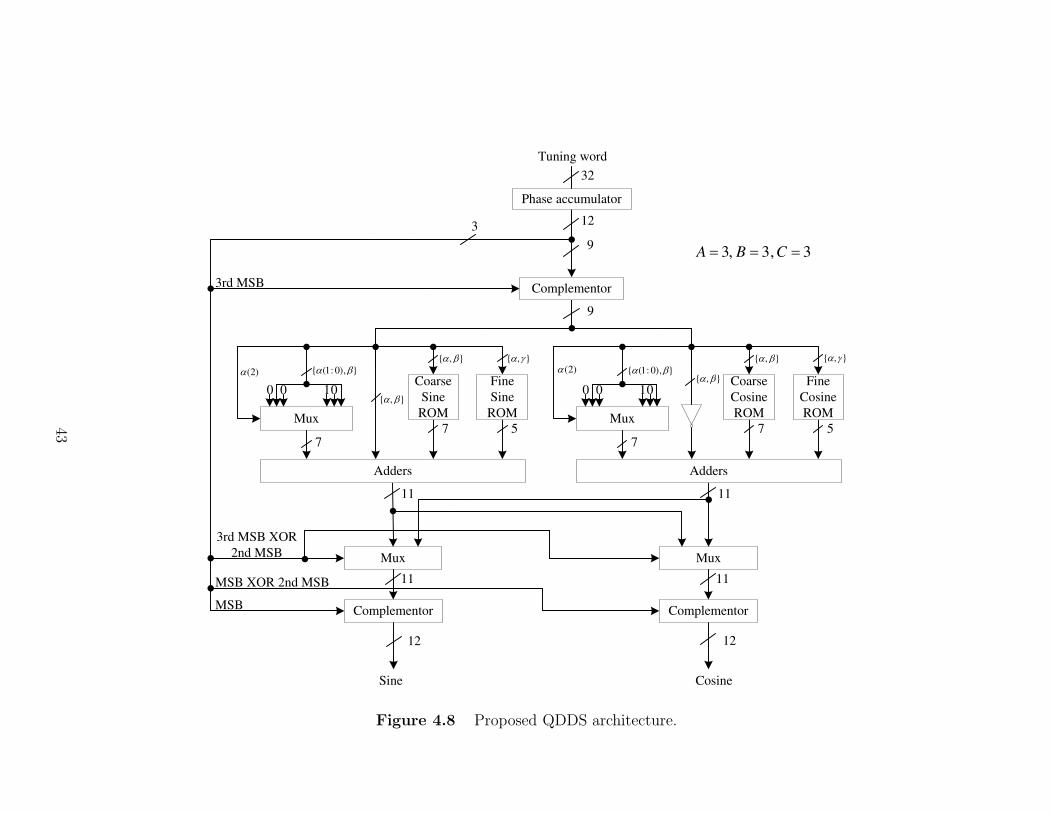
9
3rd MSB
3rd MSB XOR
2nd MSB
MSB XOR 2nd MSB
Tuning word
32
12
9
11
MSB
Sine Cosine
12 12
Phase accumulator
3
Complementor
Mux
Adders
Mux
0 0 10
)2( }),0:1({
},{
7
},{
7 5
},{)2(
11
Mux
Adders
Mux
0 0 10
}),0:1({},{
7
},{
7 5
},{
Complementor
11
Complementor
11
Coarse
Sine
ROM
Fine
Sine
ROM
Coarse
Cosine
ROM
Fine
Cosine
ROM
33,,3 CBA
Figure 4.8 Proposed QDDS architecture.
43
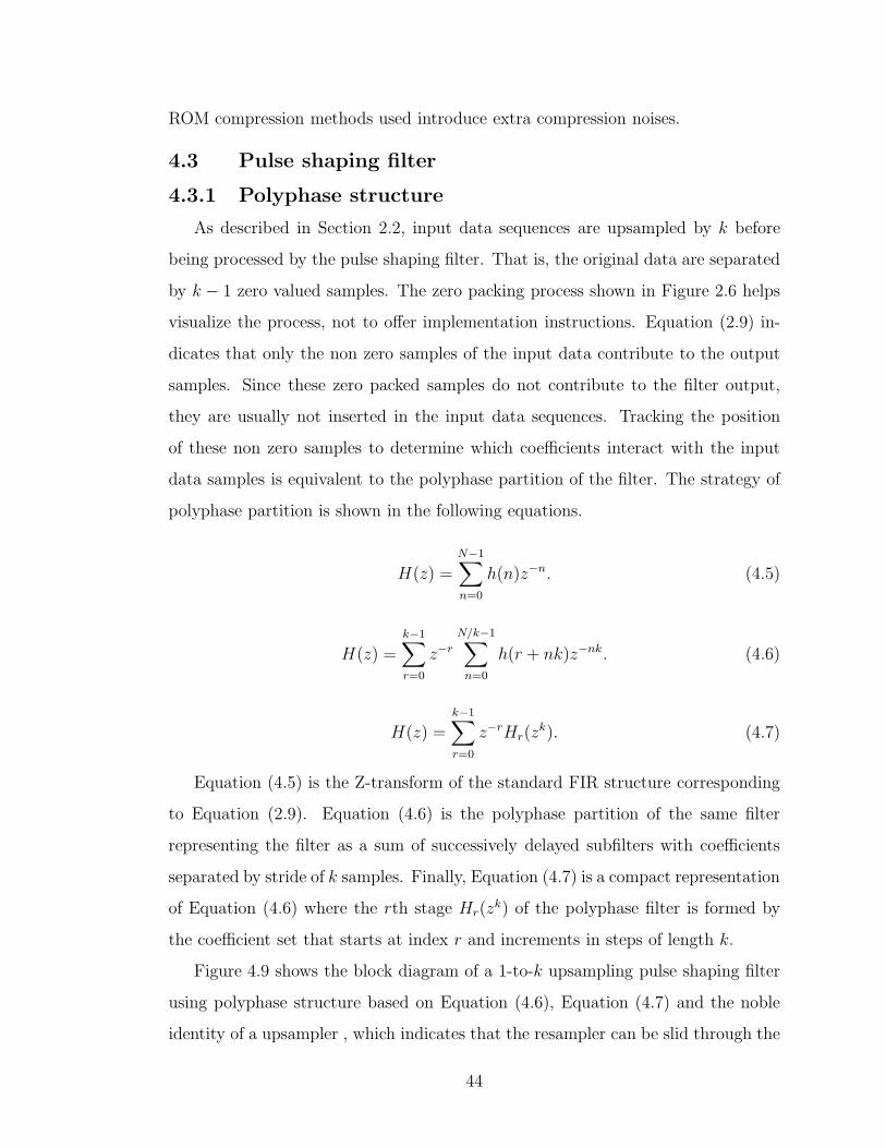
ROM compression methods used introduce extra compression noises.
4.3 Pulse shaping filter
4.3.1 Polyphase structure
As described in Section 2.2, input data sequences are upsampled by k before
being processed by the pulse shaping filter. That is, the original data are separated
by k − 1 zero valued samples. The zero packing process shown in Figure 2.6 helps
visualize the process, not to offer implementation instructions. Equation (2.9) in-
dicates that only the non zero samples of the input data contribute to the output
samples. Since these zero packed samples do not contribute to the filter output,
they are usually not inserted in the input data sequences. Tracking the position
of these non zero samples to determine which coefficients interact with the input
data samples is equivalent to the polyphase partition of the filter. The strategy of
polyphase partition is shown in the following equations.
H(z) =
N−1∑
n=0
h(n)z−n. (4.5)
H(z) =
k−1∑
r=0
z−r
N/k−1∑
n=0
h(r + nk)z−nk. (4.6)
H(z) =k−1∑
r=0
z−rHr(zk). (4.7)
Equation (4.5) is the Z-transform of the standard FIR structure corresponding
to Equation (2.9). Equation (4.6) is the polyphase partition of the same filter
representing the filter as a sum of successively delayed subfilters with coefficients
separated by stride of k samples. Finally, Equation (4.7) is a compact representation
of Equation (4.6) where the rth stage Hr(zk) of the polyphase filter is formed by
the coefficient set that starts at index r and increments in steps of length k.
Figure 4.9 shows the block diagram of a 1-to-k upsampling pulse shaping filter
using polyphase structure based on Equation (4.6), Equation (4.7) and the noble
identity of a upsampler , which indicates that the resampler can be slid through the
44

...
Coefficient Memory
r
)(nx )(my
)(zH r
)0( nkh
)1( nkh
)1( nkkh
Figure 4.9 An efficient implementation of 1-to-k upsamplingpolyphase filter.
filter and replace the k units of delay at the output clock rate with one unit delay at
the input clock rate [10]. An 1-to-k upsampling pulse shaping filter is implemented
by moving to different coefficient sets at each time.
The block diagram shown in Figure 4.9 can be further simplified by utilizing the
symmetric characteristic of the pulse shaping filter’s impulse response; thus, only
half of the coefficients needs to be stored in memory, such as register files. The user
configured coefficients are loaded into these register files during the initialization
phase.
4.3.2 Design considerations of the pulse shaping filter
The pulse shaping filters apply pulse shaping to the incoming digital signals.
An ideal SQRC shaping pulse is given in Section 2.2. Two parameters must be
considered to implement this filter in a digital system. One parameter is the filter
length after the impulse response has been delayed and truncated, and the other is
the length of the digital word to represent a coefficient. The length of the SQRC
filter determines the frequency response of the SQRC filter. If the truncated im-
pulse response is too short, then the resulting filter either can not have enough
stopband rejection, or has big ripples in the passband. Since the stopband rejection
and passband ripple are very important for most of the communication systems,
the truncated impulse response must be long enough to meet the system specifi-
45
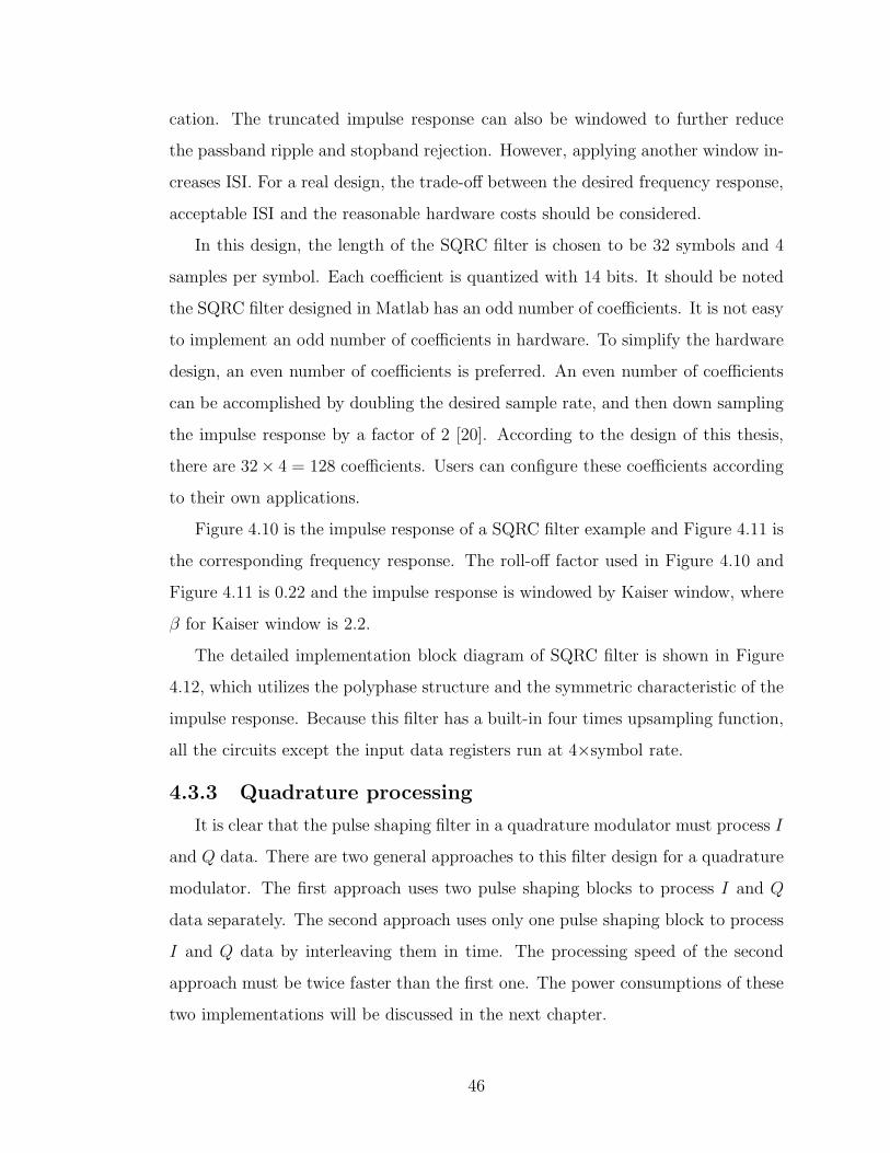
cation. The truncated impulse response can also be windowed to further reduce
the passband ripple and stopband rejection. However, applying another window in-
creases ISI. For a real design, the trade-off between the desired frequency response,
acceptable ISI and the reasonable hardware costs should be considered.
In this design, the length of the SQRC filter is chosen to be 32 symbols and 4
samples per symbol. Each coefficient is quantized with 14 bits. It should be noted
the SQRC filter designed in Matlab has an odd number of coefficients. It is not easy
to implement an odd number of coefficients in hardware. To simplify the hardware
design, an even number of coefficients is preferred. An even number of coefficients
can be accomplished by doubling the desired sample rate, and then down sampling
the impulse response by a factor of 2 [20]. According to the design of this thesis,
there are 32× 4 = 128 coefficients. Users can configure these coefficients according
to their own applications.
Figure 4.10 is the impulse response of a SQRC filter example and Figure 4.11 is
the corresponding frequency response. The roll-off factor used in Figure 4.10 and
Figure 4.11 is 0.22 and the impulse response is windowed by Kaiser window, where
β for Kaiser window is 2.2.
The detailed implementation block diagram of SQRC filter is shown in Figure
4.12, which utilizes the polyphase structure and the symmetric characteristic of the
impulse response. Because this filter has a built-in four times upsampling function,
all the circuits except the input data registers run at 4×symbol rate.
4.3.3 Quadrature processing
It is clear that the pulse shaping filter in a quadrature modulator must process I
and Q data. There are two general approaches to this filter design for a quadrature
modulator. The first approach uses two pulse shaping blocks to process I and Q
data separately. The second approach uses only one pulse shaping block to process
I and Q data by interleaving them in time. The processing speed of the second
approach must be twice faster than the first one. The power consumptions of these
two implementations will be discussed in the next chapter.
46

0 20 40 60 80 100 120
−0.1
0
0.1
0.2
0.3
0.4
0.5
n
Am
plitu
de
Figure 4.10 An example of the SQRC impulse response.
0 0.5 1 1.5 2−80
−70
−60
−50
−40
−30
−20
−10
0
Frequency normalized to symbol rate
Am
plitu
de
resp
onse
(dB
)
Figure 4.11 The frequency response of the SQRC filter whoseimpulse response is shown in Figure 4.10.
47
1z
...
...
...
Symbol
Clock
4x
Symbol
Clock)3(
)2(
(1)
)0(
h
h
h
h
)7(
)6(
(5)
)4(
h
h
h
h
)59(
)58(
(57)
)56(
h
h
h
h
)63(
)62(
(61)
)60(
h
h
h
h
)(nx
)(my
1z
1z
1z
1z
1z
1z
Figure 4.12 Block diagram of the SQRC filter.
48

4.4 Interpolation filter
The interpolation filters following the pulse shaping filter are used to increase the
sampling rate. Two hardware efficient interpolation filter structures are considered
here. One is CIC filter and the other is half-band FIR filter.
4.4.1 Design of CIC filter
As described earlier, the targeted system clock frequency is 150 MHz. The CIC
filter block diagram shown in Figure 2.8 can not meet this timing requirement. A
pipelined CIC structure is used in the system. Figure 4.13 is the block diagram of
implemented CIC filter. As shown in Equation (2.12), the frequency response of
the CIC filter depends on three factors: the rate change factor R, the order of the
filter N and the differential delay M . In the design of this thesis, M and N are
fixed at 1 and 4. The rate change factor, R, is the only variable parameter. The
available choices for R are 4, 8, 16 and 32. According to those design parameters,
Equation (2.12) which describes the CIC frequency response can be re-written as:
H(f) =
[
sin(πf)
sin(πf/R)
]4
where R ∈ {4, 8, 16, 32}. (4.8)
Figure 4.14 shows the periodic spectrum of the zero packed time series after the
processing of the pulse shaping filter and the frequency response of the 1-to-4 CIC
filter and Figure 4.15 shows the periodic spectrum of the zero packed time series
after the processing of the pulse shaping filter and the frequency response of the
1-to-8 CIC filter. One can clearly see the effect of the CIC spectral zeros on the
up-sampled input time series from the figures. It is also clear that there is frequency
dependent attenuation that the CIC filter introduces over the frequency range of
the data to be transmitted. The degree of the impact of the attenuation introduced
by CIC filter is application specific. It is shown in the result of [9] that if less
attenuation is desired, the higher rate change factor should be used. Alternatively,
data can be precompensated through a filter which has the inverse CIC frequency
response. Because the coefficients of the shaping filter are configurable, users can
combine the pulse shaping filter and the inverse CIC filter. Then the resulting
49

1z
Rf s /sfsfRf s /
1z
1z
1z
1z
1z
1z
1z
1z
1z
1z
1z
-1 -1 -1 -1
Figure 4.13 Pipelined CIC interpolation filter.
50
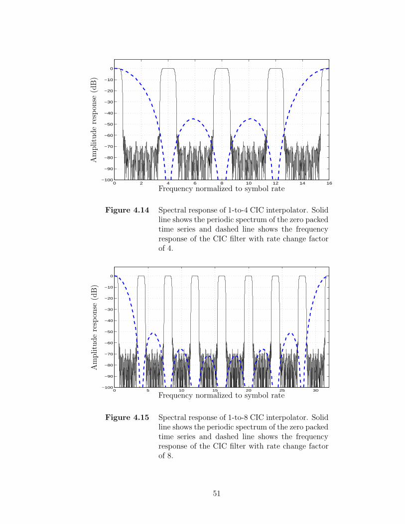
0 2 4 6 8 10 12 14 16−100
−90
−80
−70
−60
−50
−40
−30
−20
−10
0
Frequency normalized to symbol rate
Am
plitu
de
resp
onse
(dB
)
Figure 4.14 Spectral response of 1-to-4 CIC interpolator. Solidline shows the periodic spectrum of the zero packedtime series and dashed line shows the frequencyresponse of the CIC filter with rate change factorof 4.
0 5 10 15 20 25 30−100
−90
−80
−70
−60
−50
−40
−30
−20
−10
0
Frequency normalized to symbol rate
Am
plitu
de
resp
onse
(dB
)
Figure 4.15 Spectral response of 1-to-8 CIC interpolator. Solidline shows the periodic spectrum of the zero packedtime series and dashed line shows the frequencyresponse of the CIC filter with rate change factorof 8.
51

impulse response of the shaping filter should be the convolution of the two impulse
responses, the impulse response of the pulse shaping filter and the impulse response
of the inverse CIC filter.
As mentioned earlier, the CIC filter is designed to handle rate change factors of
R = 4, 8, 16 and 32. The input and output register widths are all 12 bits. Since
the same filter will be used over a range of rate change factors, maximum register
widths must be chosen over all the rate change factors. These maximum widths
occur at the maximum rate change factor, i.e., R = 32. The register widths are
calculated according to Equation (2.13) and Equation (2.15). The register widths
for each stage are 13, 14, 15, 15, 15, 19, 23 and 27 respectively. The number of
LSB’s discarded going into the output register is 6, 9, 12 and 15 for the rate change
factor of 4, 8, 16 and 32, respectively.
4.4.2 Design of half-band filter
To reach the similar image rejection ratio of the designed 4th order CIC filter,
the length of the half-band FIR filter is at least 13. Since the interpolation ratio
of the designed CIC filter is limited to 4, 8, 16 and 32, two-, three-, four- and five-
half-band FIR filters can be cascaded to achieve the same interpolation ratio as the
CIC filter.
Figure 4.16 shows the periodic spectrum of the zero packed time series after the
processing of the pulse shaping filter and the frequency response of two cascaded
half-band FIR filters. Figure 4.17 shows the periodic spectrum of the zero packed
time series after the processing of the pulse shaping filter and the frequency response
of three cascaded half-band FIR filters.
The half-band FIR filter of the length of 13 is implemented according to the
polyphase half-band FIR filter shown in [10]. The input data sequence is theoret-
ically upsampled by 2 before being processed by a half-band filter, i.e., one zero
valued sample is inserted between two input samples. This is very similar to the
situation described in Section 4.3.1; thus, the half-band filter can also be parti-
tioned into a pair of polyphase filters instead of inserting zero valued samples. The
52
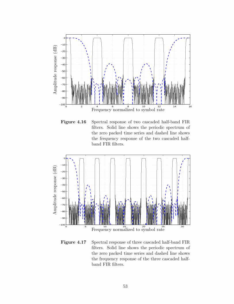
0 2 4 6 8 10 12 14 16−100
−90
−80
−70
−60
−50
−40
−30
−20
−10
0
Frequency normalized to symbol rate
Am
plitu
de
resp
onse
(dB
)
Figure 4.16 Spectral response of two cascaded half-band FIRfilters. Solid line shows the periodic spectrum ofthe zero packed time series and dashed line showsthe frequency response of the two cascaded half-band FIR filters.
0 5 10 15 20 25 30−100
−90
−80
−70
−60
−50
−40
−30
−20
−10
0
Frequency normalized to symbol rate
Am
plitu
de
resp
onse
(dB
)
Figure 4.17 Spectral response of three cascaded half-band FIRfilters. Solid line shows the periodic spectrum ofthe zero packed time series and dashed line showsthe frequency response of the three cascaded half-band FIR filters.
53
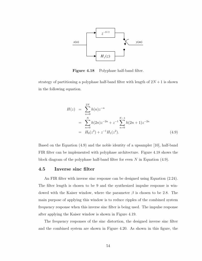
2/Nz
)(1 zH
)(nx )(my
Figure 4.18 Polyphase half-band filter.
strategy of partitioning a polyphase half-band filter with length of 2N +1 is shown
in the following equation.
H(z) =
2N∑
n=0
h(n)z−n
=N∑
n=0
h(2n)z−2n + z−1N−1∑
n=0
h(2n + 1)z−2n
= H0(z2) + z−1H1(z
2). (4.9)
Based on the Equation (4.9) and the noble identity of a upsampler [10], half-band
FIR filter can be implemented with polyphase architecture. Figure 4.18 shows the
block diagram of the polyphase half-band filter for even N in Equation (4.9).
4.5 Inverse sinc filter
An FIR filter with inverse sinc response can be designed using Equation (2.24).
The filter length is chosen to be 9 and the synthesized impulse response is win-
dowed with the Kaiser window, where the parameter β is chosen to be 2.8. The
main purpose of applying this window is to reduce ripples of the combined system
frequency response when this inverse sinc filter is being used. The impulse response
after applying the Kaiser window is shown in Figure 4.19.
The frequency responses of the sinc distortion, the designed inverse sinc filter
and the combined system are shown in Figure 4.20. As shown in this figure, the
54
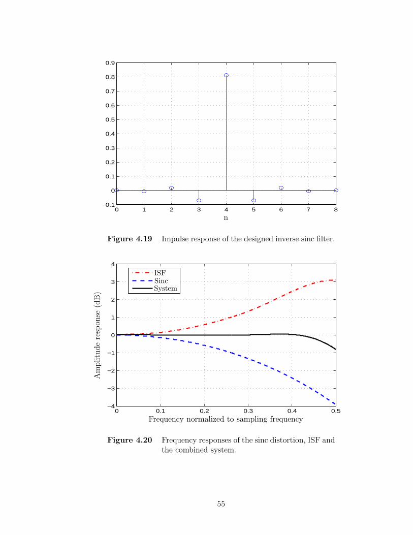
0 1 2 3 4 5 6 7 8−0.1
0
0.1
0.2
0.3
0.4
0.5
0.6
0.7
0.8
0.9
n
Figure 4.19 Impulse response of the designed inverse sinc filter.
0 0.1 0.2 0.3 0.4 0.5−4
−3
−2
−1
0
1
2
3
4
Frequency normalized to sampling frequency
Am
plitu
de
resp
onse
(dB
)
ISFSincSystem
Figure 4.20 Frequency responses of the sinc distortion, ISF andthe combined system.
55

designed inverse sinc filter can compensate for the sinc distortion and maintain the
flat output amplitude (less than 0.1 dB) over the bandwidth of 0 to 80% of the first
Nyquist zone. Using longer filter to implement this inverse sinc filter can lead to
less ripple and wider working bandwidth. For example, if the filter is implemented
with the length of 19, the ripple is less than 0.04 dB over the bandwidth of 0 to
90% of the first Nyquist zone. However, for high clock speed, longer length will
increase the complexity of the filter and consume more power.
It should also be noted that the inverse sinc filter exhibits an insertion loss of
about 3 dB. Thus, signal levels at the output port with this filter bypassed are 3 dB
higher than with this filter engaged. For relatively wide bandwidth application,
the benefits of the inverse sinc compensation usually outweighs the 3 dB loss in
the output level. The decision of using this filter or not is related to the specific
application.
In order to implement this filter, the coefficients have to be quantized first. The
coefficients that are scaled to represent integers are listed in Table 4.3. Since the
impulse response of this filter is symmetrical about the center, the signal flow for
FIR filter shown in Figure 2.5 can be simplified. As shown in Figure 4.21, in order to
reduce the number of multipliers, the symmetrical taps outputs are added together
before they are multiplied by the coefficients.
Table 4.3 Coefficients for the designed inverse sinc filter.
h(n) Coefficients Scaled coefficients(12-bit quantization)
h(0) = h(8) 0.0016 3
h(1) = h(7) -0.0057 -12
h(2) = h(6) 0.0179 37
h(3) = h(5) -0.0693 -142
h(4) 0.8109 1660
56
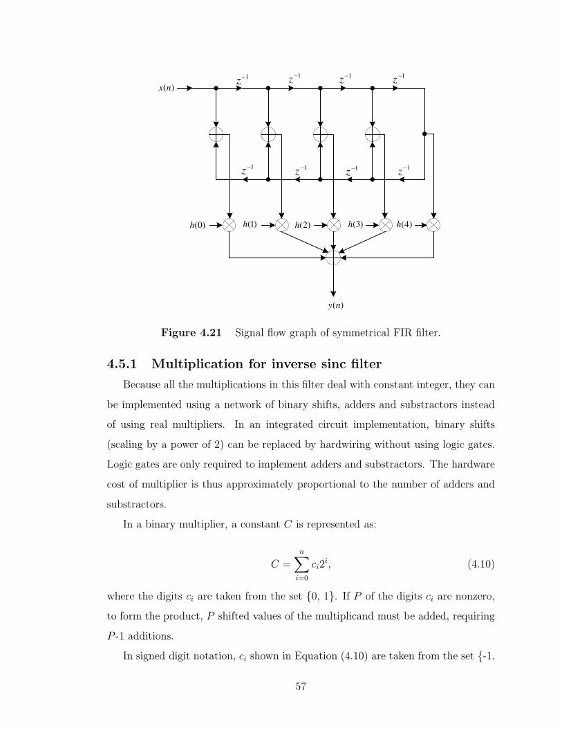
)(nx
)(ny
1z
)0(h )1(h )2(h )3(h )4(h
1z 1
z 1z
1z
1z 1
z1
z
Figure 4.21 Signal flow graph of symmetrical FIR filter.
4.5.1 Multiplication for inverse sinc filter
Because all the multiplications in this filter deal with constant integer, they can
be implemented using a network of binary shifts, adders and substractors instead
of using real multipliers. In an integrated circuit implementation, binary shifts
(scaling by a power of 2) can be replaced by hardwiring without using logic gates.
Logic gates are only required to implement adders and substractors. The hardware
cost of multiplier is thus approximately proportional to the number of adders and
substractors.
In a binary multiplier, a constant C is represented as:
C =n∑
i=0
ci2i, (4.10)
where the digits ci are taken from the set {0, 1}. If P of the digits ci are nonzero,
to form the product, P shifted values of the multiplicand must be added, requiring
P -1 additions.
In signed digit notation, ci shown in Equation (4.10) are taken from the set {-1,
57
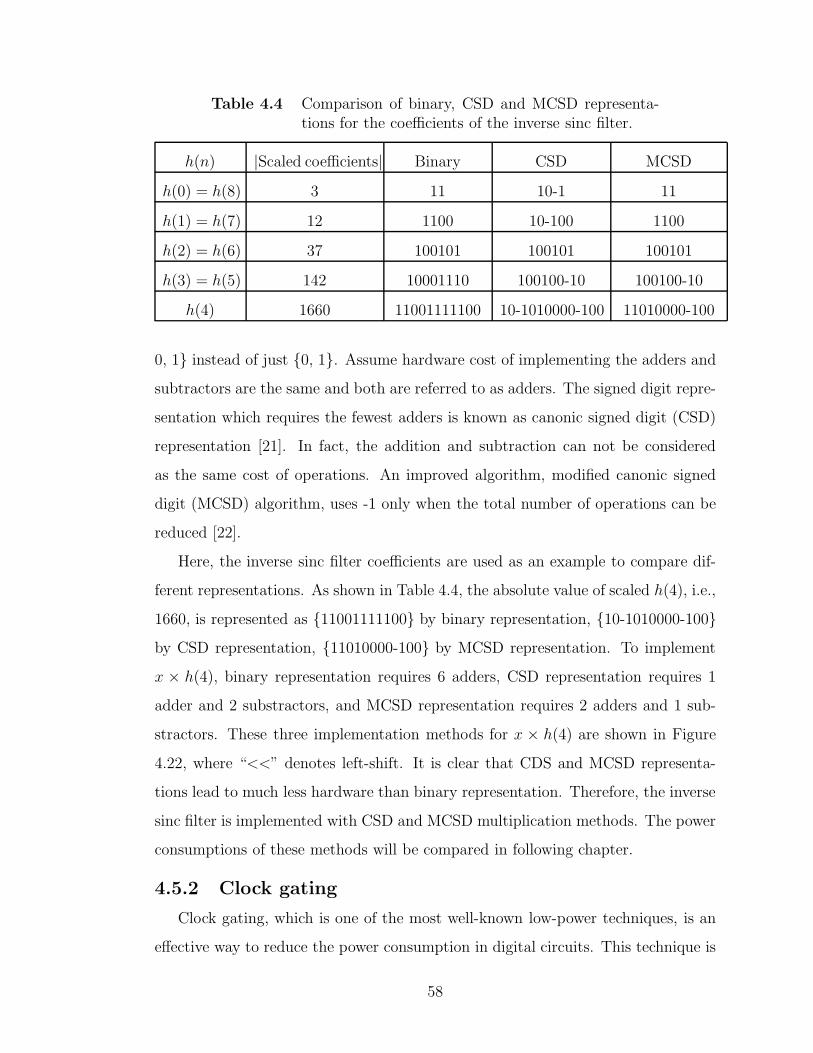
Table 4.4 Comparison of binary, CSD and MCSD representa-tions for the coefficients of the inverse sinc filter.
h(n) |Scaled coefficients| Binary CSD MCSD
h(0) = h(8) 3 11 10-1 11
h(1) = h(7) 12 1100 10-100 1100
h(2) = h(6) 37 100101 100101 100101
h(3) = h(5) 142 10001110 100100-10 100100-10
h(4) 1660 11001111100 10-1010000-100 11010000-100
0, 1} instead of just {0, 1}. Assume hardware cost of implementing the adders and
subtractors are the same and both are referred to as adders. The signed digit repre-
sentation which requires the fewest adders is known as canonic signed digit (CSD)
representation [21]. In fact, the addition and subtraction can not be considered
as the same cost of operations. An improved algorithm, modified canonic signed
digit (MCSD) algorithm, uses -1 only when the total number of operations can be
reduced [22].
Here, the inverse sinc filter coefficients are used as an example to compare dif-
ferent representations. As shown in Table 4.4, the absolute value of scaled h(4), i.e.,
1660, is represented as {11001111100} by binary representation, {10-1010000-100}by CSD representation, {11010000-100} by MCSD representation. To implement
x × h(4), binary representation requires 6 adders, CSD representation requires 1
adder and 2 substractors, and MCSD representation requires 2 adders and 1 sub-
stractors. These three implementation methods for x × h(4) are shown in Figure
4.22, where “<<” denotes left-shift. It is clear that CDS and MCSD representa-
tions lead to much less hardware than binary representation. Therefore, the inverse
sinc filter is implemented with CSD and MCSD multiplication methods. The power
consumptions of these methods will be compared in following chapter.
4.5.2 Clock gating
Clock gating, which is one of the most well-known low-power techniques, is an
effective way to reduce the power consumption in digital circuits. This technique is
58

<<2<<3<<4<<5<<6<<9<<10
x
(a) Binary multiplication
<<2<<7<<9<<11
x
--
(b) CSD multiplication
<<2<<7<<9<<10
x
-
(c) MCSD multiplication
Figure 4.22 Comparison of the three different ways to imple-ment x × h(4).
also implemented in Synopsys Power Compiler [23]. The goal of this technique is
to disable or suppress transitions from propagating to parts of a clock path under
a certain condition. The dynamic power of a digital Complementary Metal Oxide
Silicon (CMOS) circuit is proportional to clock frequency and the square of the
supply voltage [24]. Power can be saved by reducing the clock frequency (in the
limit by stopping), or by reducing the supply voltage (in the limit by powering off
the components). Note that the two limiting cases, clocking freezing and powering
off, are applicable to idle components [25]. When there are idle digital components,
clock gating is a commonly used technique for saving power. Clock gating technique
59
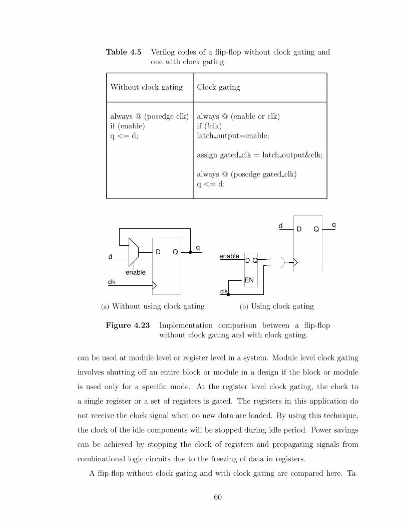
Table 4.5 Verilog codes of a flip-flop without clock gating andone with clock gating.
Without clock gating Clock gating
always @ (posedge clk) always @ (enable or clk)if (enable) if (!clk)q <= d; latch output=enable;
assign gated clk = latch output&clk;
always @ (posedge gated clk)q <= d;
D Qd
enable
q
clk
(a) Without using clock gating
D Qd
enable
q
D Q
EN
clk
(b) Using clock gating
Figure 4.23 Implementation comparison between a flip-flopwithout clock gating and with clock gating.
can be used at module level or register level in a system. Module level clock gating
involves shutting off an entire block or module in a design if the block or module
is used only for a specific mode. At the register level clock gating, the clock to
a single register or a set of registers is gated. The registers in this application do
not receive the clock signal when no new data are loaded. By using this technique,
the clock of the idle components will be stopped during idle period. Power savings
can be achieved by stopping the clock of registers and propagating signals from
combinational logic circuits due to the freezing of data in registers.
A flip-flop without clock gating and with clock gating are compared here. Ta-
60

enable
clk
latch output
gated clock
Figure 4.24 The mechanism of using latch to prevent the glitchon the gated clock net.
ble 4.5 shows Verilog code comparison and Figure 4.23 shows the corresponding
implementations.
As shown in Figure 4.23, a latch and an AND gate are used in the clock gating
implementation. The main reason for using a latch is to prevent the glitches on
the gated clock since its changes happen during the low phase of the clock. This
mechanism is shown in Figure 4.24. When the clock is low, the latch is enabled.
The enable input is propagated to the latch output. In the mean time, when
the clock arrives, it gets propagated to the gated clock net, without any glitches
because the latch output is stable for sufficient time to meet the flip-flop’s setup
requirements. When the enable input goes low, output from the AND gate and is
also low preventing the clock from being propagated to the gated clock net. This
makes the gated clock net to be low without any switching activity.
Since whether to use the inverse sinc filter block is application dependant, mod-
ule level clock gating technique is used to shut off the clock signal for this block
when users choose not to use it. The block diagram is similar to the one shown in
Figure 4.23(b) except that the register is replaced with the inverse sinc filter block.
4.6 Multipliers
Since the frequency of the output IF signal is tunable, real digital multipliers are
required to multiply the outputs of the QDDS and the outputs of the interpolation
61
filters. There are 6 different digital multipliers available in the Synopsys Design-
Ware library, which is a broad portfolio of synthesizable implementation intellectual
properties (IPs) for ASIC, system on chip (SOC) and FPGA design [26], including
DW02 mult, DW02 mult 2 stage, DW02 mult 3 stage, DW02 mult 4 stage, DW02
mult 5 stage and DW02 mult 6 stage. Synopsys Design Compiler maps “∗” in
HDL code to DW02 mult by default. DW02 mult is a totally combinational cir-
cuit, which has the parameterized word length and unsigned or signed (two’s-
complement) data operation selection. During the logic synthesis process, Design
Compiler selects the appropriate combinational circuit architecture according to
the constraints set by users. Other multipliers available in the DesignWare library
are all pipelined multipliers. For example, DW02 mult 3 stage is a three stage
pipelined multiplier, which produces a product with a latency of two clock cycles.
These pipelined multipliers also have the parameterized word length and unsigned
or signed (two’s-complement) data operation selection. It should be noted that for
automatic pipeline retiming the combinational circuits in these pipelined multipliers
are different from the one in DW02 mult.
It is found that the resulting circuit using DW02 mult does not meet the timing
requirements for the design of this thesis. As a result, a pipelined multiplier is
necessary for the design. Also, the automatic pipeline retiming technique has to be
used to optimize the timing. This automatic pipeline retiming can be achieved by
using the special register retiming command in Design Compiler.
The compile command in Design Compiler optimizes combinational logic by
performing Boolean optimization and mapping the design to the target technology
library. The optimization leaves unchanged the location and number of any registers
present in the design. To further improve the circuit timing, register retiming
technique can be used. Register retiming is a sequential optimization technique
that moves registers through the combinational logic gates of a design to optimize
timing and area. Designers can determine the optimal register locations and code
them into the HDL description. However, it is difficult to find the optimal register
locations inside a multiplier in the DesignWare library without total understanding
62
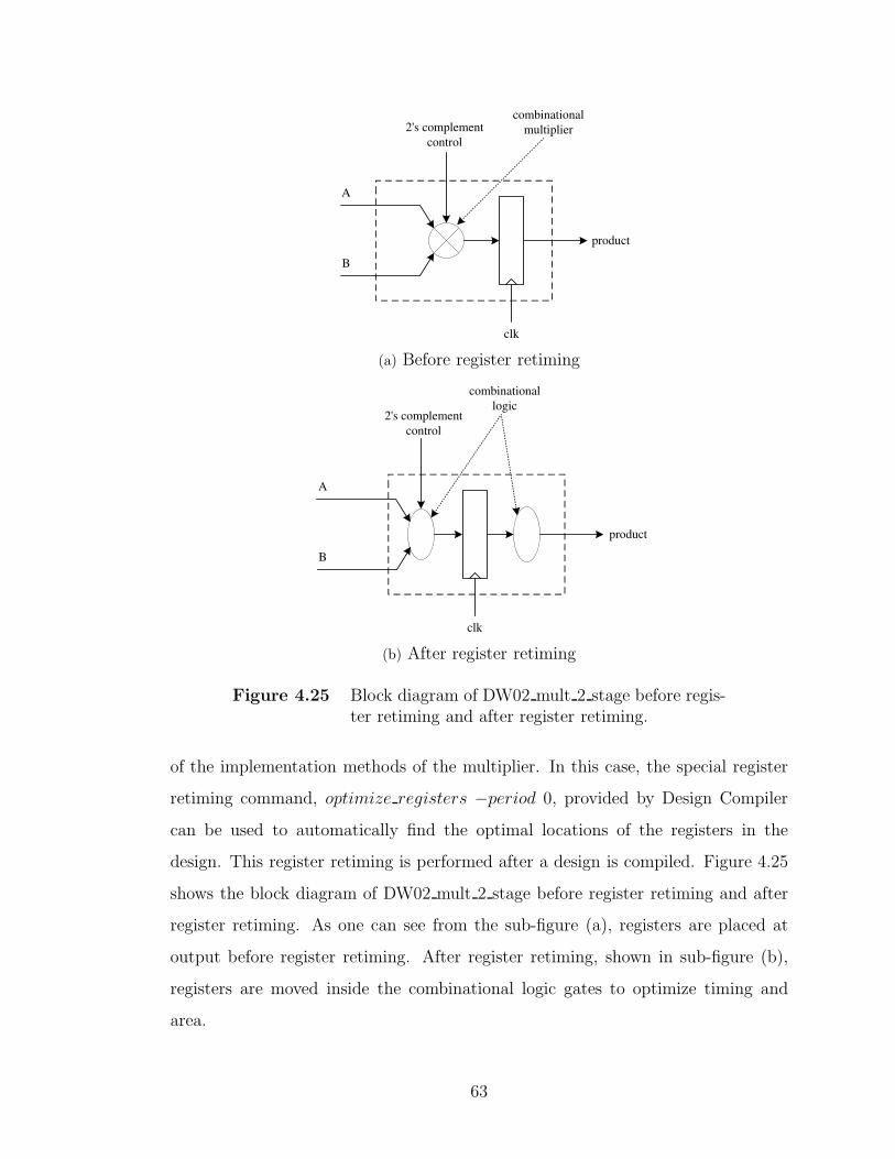
A
B
clk
product
2's complement
control
combinational
multiplier
(a) Before register retiming
clk
B
A
product
2's complement
control
combinational
logic
(b) After register retiming
Figure 4.25 Block diagram of DW02 mult 2 stage before regis-ter retiming and after register retiming.
of the implementation methods of the multiplier. In this case, the special register
retiming command, optimize registers −period 0, provided by Design Compiler
can be used to automatically find the optimal locations of the registers in the
design. This register retiming is performed after a design is compiled. Figure 4.25
shows the block diagram of DW02 mult 2 stage before register retiming and after
register retiming. As one can see from the sub-figure (a), registers are placed at
output before register retiming. After register retiming, shown in sub-figure (b),
registers are moved inside the combinational logic gates to optimize timing and
area.
63

The multipliers in this design are implemented with DW02 mult 2 stage and
DW02 mult 3 stage. Although the results show that both implementations can
meet the timing requirements after register retiming, the implementation using
DW02 mult 3 stage consuming more power and area. As the result, DW02 mult 2 stage
with register timing is chosen as the multiplier in this modulator.
4.7 Summary
The implementation of all the key blocks in the modulator are elaborated. A
novel QDDS architecture is proposed, which combines Suntherland algorithm, sine
phase difference method and QLA method to compress ROM size. For the im-
plementation of pulse shaping filter, two general design approaches are introduced.
One approach uses two pulse shaping blocks to process I/Q data and the other uses
one pulse shaping block by interleaving I/Q data. The implementation of pipelined
CIC filter and polyphase half-band filter are covered. For the implementation of the
inverse sinc filter, CSD multiplication and MCSD multiplication are used to imple-
ment the multipliers inside. Clock gating technique is also used to save power when
the inverse sinc filter is not being used. The implementation of digital multipliers
in the modulator is also discussed in this chapter.
64
Chapter 5
Performance Evaluation
As described in Chapter 4, there are different design options for each block.
The performance of these design choices will be compared in this chapter with
an emphasis on power consumption. To this end, a high-level power estimation
technique is described. The technique can be used as a fast power consumption
comparison for different design choices. The design choice which leads to less power
consumption will be integrated together to achieve a low-power modulator.
5.1 High-level power estimation
5.1.1 Sources of power consumption
Power consumption in an integrated circuit has two components, dynamic power
consumption and static power consumption. Dynamic power is dissipated when a
device is switching. Switched capacitance power comes from charging and discharg-
ing capacitive loads. The calculation of the switched capacitance power is shown
in Equation (5.1), where Cload is the capacitive load, α models the switching prob-
ability during a cycle of the clock toggling at frequency f and Vdd is the supply
voltage. Short-circuit power is the second part of the dynamic power consumption.
It is dissipated due to the current that conducts when both pull-up and pull-down
networks are momentarily conducting at the same time. Equation (5.2) gives a
simple model of the short circuit power, where β models the transistors’ conduc-
tivity per voltage factoring the linear region, T is the inputs’ rise/fall time, and τ
is the gate delay [24]. Leakage power, which is the major source of static power
consumption, is mostly due to leakage currents flowing through the channel even
65
when the gate-source voltage is below threshold voltage.
P =1
2· Cload · α · V 2
dd · f (5.1)
Psc =β
12(Vdd − 2Vth)
3 τ
T(5.2)
According to the data shown in [24], the power consumption for integrated cir-
cuits at 0.18µm and larger technology is still dominated by the dynamic power
consumption. However, the leakage power has to be considered for a design using
0.13µm or more advanced technology [27]. For the design presented in this thesis,
the modulator is implemented with 0.18µm technology. All the low-power methods
used are trying to save the dynamic power because dynamic power consumption
dominates in this technology. Note that some dynamic power efficient implementa-
tions actually lead to increasing leakage power consumption.
5.1.2 Power estimation and analysis flow
Generally speaking, all the tools for switched capacitance power consumption
estimation need to evaluate Equation (5.1). This can be done at different lev-
els of abstraction, such as algorithm level, RTL level, gate level or circuit level.
Power calculator collects the parameters of Equation (5.1) at the respective level
of abstraction. Floorplan and the architecture determine the physical and struc-
tural architecture and represent the capacitance Cload in Equation (5.1). Activity
calculator produces an activation profile for each of the components modeling the
switching probability, α in Equation (5.1). Finally, the supply voltage Vdd and the
clock frequency f are provided by the designer. For accurate short circuit power
and leakage power estimation, transistor level models are necessary.
For the power consumption estimation in this thesis, a fast comparison of dif-
ferent design options is desired. The primary goal of this thesis is to know which
design option should be chosen to follow. Thus, relative power consumption figures
for each of the design options are needed. Although the predicted power figure of
66
the different options may differ to some extent from the final power figure after im-
plementation, it is important that the estimated most power efficient option really
leads to the least power consumption. Based on this consideration, the gate level
power estimation is chosen.
5.1.3 Power estimation in logic synthesizer
The power estimation flow of Synopsys Design Compiler is shown in Figure 5.1.
After performing synthesis, Synopsys Design Compiler uses the synthesized gate
level netlist to estimate the power consumption. The dynamic power considered by
Synopsys Design Compiler includes net switching power and cell internal power. Net
switching power is computed according to Equation (5.1). Capacitance is computed
based on the capacitance specified in library cells and wire-load model. The cell
internal power includes the power consumed due to switching activities on internal
nodes of cells and the short circuit power consumed by the cells. The leakage power
is estimated according to the leakage power annotation for each cell in the library.
The leakage power annotations may vary with different input states of one cell
because leakage model can be state dependant [24, 27].
The two most significant sources of inaccuracy at the gate level power estimation
are the switching activities and the prelayout wire-load values [28]. There are two
ways to estimate the switching activities, vector analysis and vectorless analysis.
For the vector analysis, the switching activities can be estimated from simulation
data. For the vectorless analysis, power estimator annotates the switching activity
for the ports and propagates this value through the design based on statistical
calculations.
The vector analysis has several limitations. First, for large design, circuit sim-
ulation is very time consuming. Second, it is difficult to determine if the test cases
causing the highest power consumption are covered by simulation data. Since the
goal is to compute the relative power consumption figures for each design option, the
vectorless power analysis is chosen. The Synopsys Design Compiler uses the default
switching activity (0.25 toggle per positive edge) for the ports and the wire-load
67
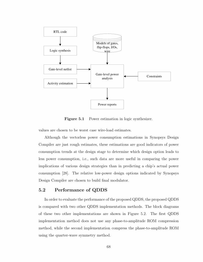
RTL code
Logic synthesis
Gate-level netlist
Gate-level power
analysis
Activity estimation
Models of gates,
flip-flops, I/Os,
wire
Constraints
Power reports
Figure 5.1 Power estimation in logic synthesizer.
values are chosen to be worst case wire-load estimates.
Although the vectorless power consumption estimations in Synopsys Design
Compiler are just rough estimates, these estimations are good indicators of power
consumption trends at the design stage to determine which design option leads to
less power consumption, i.e., such data are more useful in comparing the power
implications of various design strategies than in predicting a chip’s actual power
consumption [28]. The relative low-power design options indicated by Synopsys
Design Compiler are chosen to build final modulator.
5.2 Performance of QDDS
In order to evaluate the performance of the proposed QDDS, the proposed QDDS
is compared with two other QDDS implementation methods. The block diagrams
of these two other implementations are shown in Figure 5.2. The first QDDS
implementation method does not use any phase-to-amplitude ROM compression
method, while the second implementation compress the phase-to-amplitude ROM
using the quarter-wave symmetry method.
68
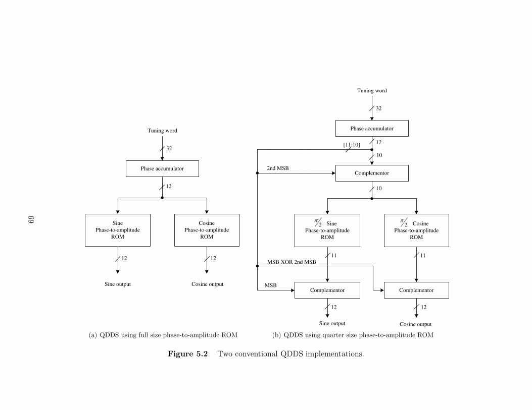
Tuning word
32
Phase accumulator
Sine
Phase-to-amplitude
ROM
12
Cosine
Phase-to-amplitude
ROM
12 12
Sine output Cosine output
(a) QDDS using full size phase-to-amplitude ROM
Tuning word
32
Phase accumulator
Sine
Phase-to-amplitude
ROM
12
Cosine
Phase-to-amplitude
ROM
11 11
Sine output Cosine output
Complementor
10
[11:10]
2nd MSB
10
Complementor Complementor
1212
MSB
MSB XOR 2nd MSB
22
(b) QDDS using quarter size phase-to-amplitude ROM
Figure 5.2 Two conventional QDDS implementations.
69
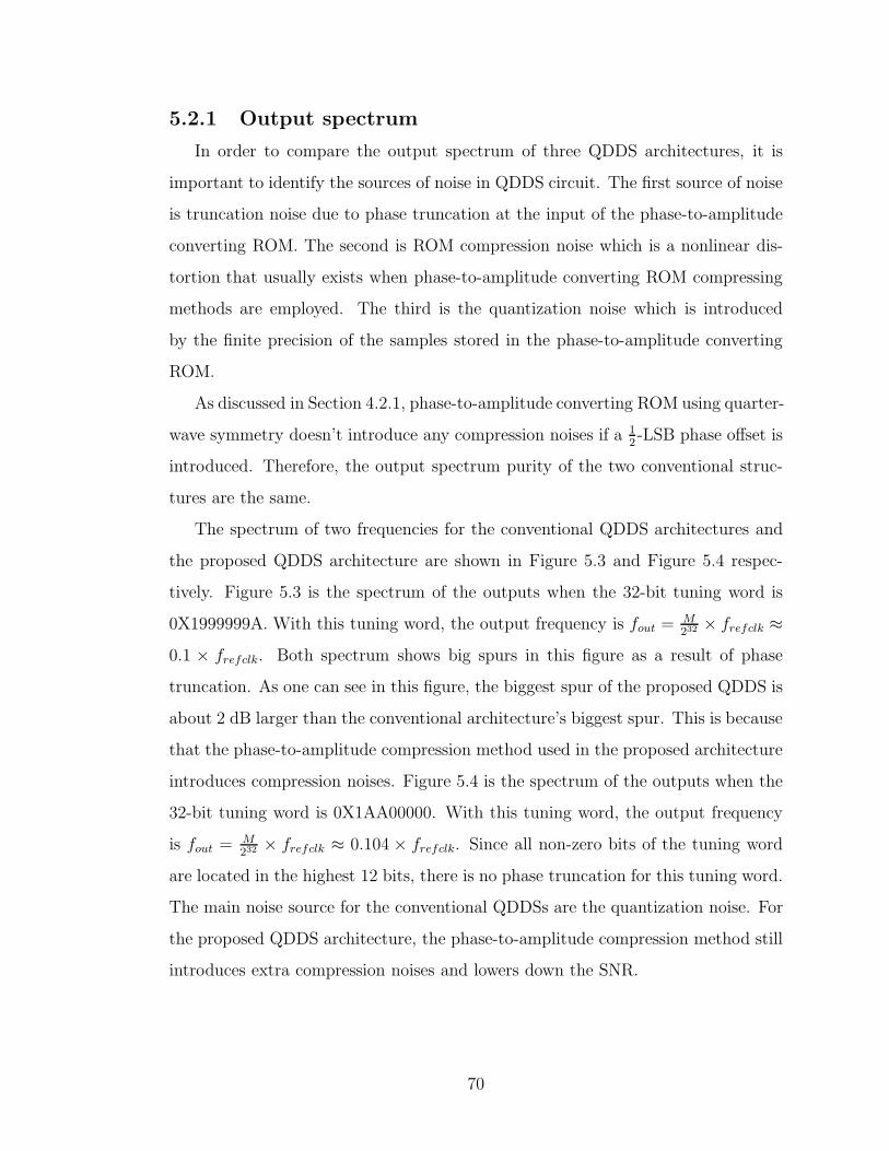
5.2.1 Output spectrum
In order to compare the output spectrum of three QDDS architectures, it is
important to identify the sources of noise in QDDS circuit. The first source of noise
is truncation noise due to phase truncation at the input of the phase-to-amplitude
converting ROM. The second is ROM compression noise which is a nonlinear dis-
tortion that usually exists when phase-to-amplitude converting ROM compressing
methods are employed. The third is the quantization noise which is introduced
by the finite precision of the samples stored in the phase-to-amplitude converting
ROM.
As discussed in Section 4.2.1, phase-to-amplitude converting ROM using quarter-
wave symmetry doesn’t introduce any compression noises if a 12-LSB phase offset is
introduced. Therefore, the output spectrum purity of the two conventional struc-
tures are the same.
The spectrum of two frequencies for the conventional QDDS architectures and
the proposed QDDS architecture are shown in Figure 5.3 and Figure 5.4 respec-
tively. Figure 5.3 is the spectrum of the outputs when the 32-bit tuning word is
0X1999999A. With this tuning word, the output frequency is fout = M232 × frefclk ≈
0.1 × frefclk. Both spectrum shows big spurs in this figure as a result of phase
truncation. As one can see in this figure, the biggest spur of the proposed QDDS is
about 2 dB larger than the conventional architecture’s biggest spur. This is because
that the phase-to-amplitude compression method used in the proposed architecture
introduces compression noises. Figure 5.4 is the spectrum of the outputs when the
32-bit tuning word is 0X1AA00000. With this tuning word, the output frequency
is fout = M232 × frefclk ≈ 0.104 × frefclk. Since all non-zero bits of the tuning word
are located in the highest 12 bits, there is no phase truncation for this tuning word.
The main noise source for the conventional QDDSs are the quantization noise. For
the proposed QDDS architecture, the phase-to-amplitude compression method still
introduces extra compression noises and lowers down the SNR.
70
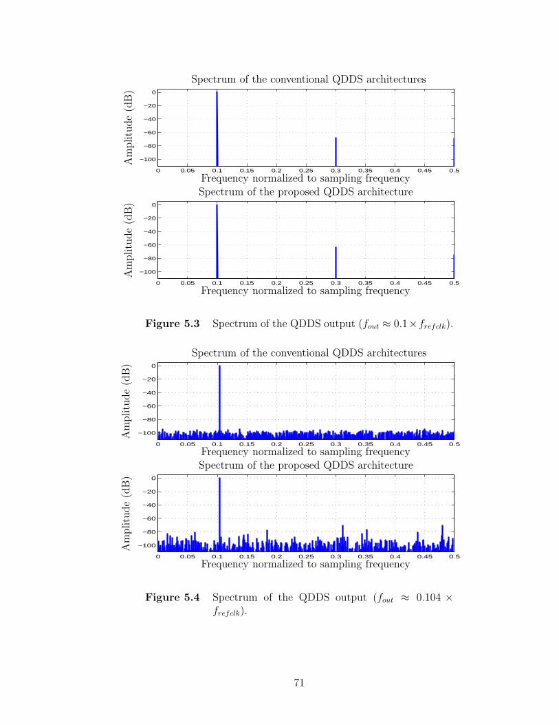
0 0.05 0.1 0.15 0.2 0.25 0.3 0.35 0.4 0.45 0.5
−100
−80
−60
−40
−20
0
0 0.05 0.1 0.15 0.2 0.25 0.3 0.35 0.4 0.45 0.5
−100
−80
−60
−40
−20
0
Frequency normalized to sampling frequency
Frequency normalized to sampling frequency
Am
plitu
de
(dB
)A
mplitu
de
(dB
)
Spectrum of the conventional QDDS architectures
Spectrum of the proposed QDDS architecture
Figure 5.3 Spectrum of the QDDS output (fout ≈ 0.1×frefclk).
0 0.05 0.1 0.15 0.2 0.25 0.3 0.35 0.4 0.45 0.5
−100
−80
−60
−40
−20
0
0 0.05 0.1 0.15 0.2 0.25 0.3 0.35 0.4 0.45 0.5
−100
−80
−60
−40
−20
0
Frequency normalized to sampling frequency
Frequency normalized to sampling frequency
Am
plitu
de
(dB
)A
mplitu
de
(dB
)
Spectrum of the conventional QDDS architectures
Spectrum of the proposed QDDS architecture
Figure 5.4 Spectrum of the QDDS output (fout ≈ 0.104 ×frefclk).
71
50 60 70 80 90 100 110 120 130 140 1500
50
100
150
200
250
System clock frequency (MHz)
Pow
erco
nsu
mpti
on(m
W)
QDDS with full size ROMQDDS using quarter-wave symmetryQDDS with proposed architecture
Figure 5.5 Power consumption comparison for 3 differentQDDS architectures.
5.2.2 Power consumption
Figure 5.5 shows the power consumption of three different QDDS architectures.
As one can see from this figure, the proposed QDDS can save up to 90% power
consumption at 150 MHz compared with the QDDS which uses full size ROM, and
can save up to 60% power consumption at 150 MHz compared with the QDDS
which uses quarter-wave symmetry. Reports from logic synthesizer also show that
the proposed QDDS can save area compared with the conventional ones. The
proposed QDDS can save up to 98% area compared with the design which uses
full size ROM, and can save up to 91% area compared with the design which uses
quarter-wave symmetry.
5.3 Performance of pulse shaping filter
As described in Section 4.3.3, there are two general approaches to design the
pulse shaping filter for a quadrature modulator. One approach requires two pulse
shaping filter blocks to process the I/Q data separately, while the other approach
requires only one pulse shaping filter block by interleaving the data in time. When
72
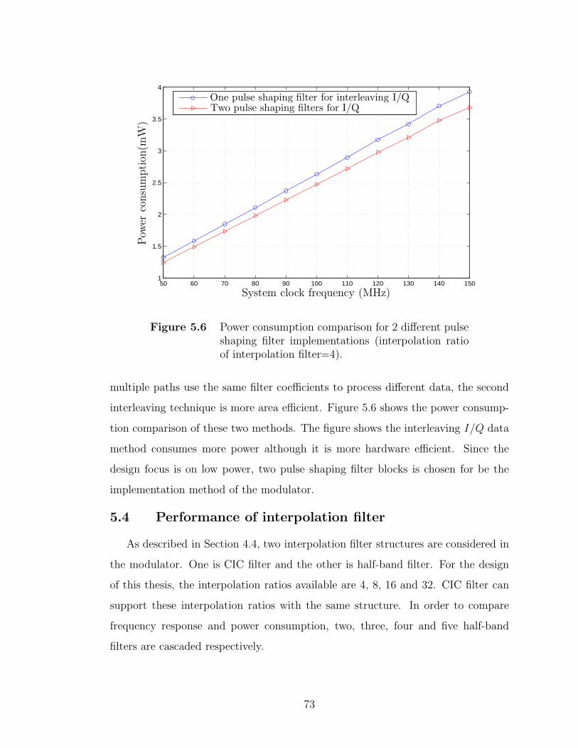
50 60 70 80 90 100 110 120 130 140 1501
1.5
2
2.5
3
3.5
4
System clock frequency (MHz)
Pow
erco
nsu
mpti
on(m
W)
One pulse shaping filter for interleaving I/QTwo pulse shaping filters for I/Q
Figure 5.6 Power consumption comparison for 2 different pulseshaping filter implementations (interpolation ratioof interpolation filter=4).
multiple paths use the same filter coefficients to process different data, the second
interleaving technique is more area efficient. Figure 5.6 shows the power consump-
tion comparison of these two methods. The figure shows the interleaving I/Q data
method consumes more power although it is more hardware efficient. Since the
design focus is on low power, two pulse shaping filter blocks is chosen for be the
implementation method of the modulator.
5.4 Performance of interpolation filter
As described in Section 4.4, two interpolation filter structures are considered in
the modulator. One is CIC filter and the other is half-band filter. For the design
of this thesis, the interpolation ratios available are 4, 8, 16 and 32. CIC filter can
support these interpolation ratios with the same structure. In order to compare
frequency response and power consumption, two, three, four and five half-band
filters are cascaded respectively.
73

0 2 4 6 8 10 12 14 16−100
−80
−60
−40
−20
0
0 2 4 6 8 10 12 14 16−100
−80
−60
−40
−20
0
Frequency normalized to symbol rate
Frequency normalized to symbol rate
Am
plitu
de
(dB
)A
mplitu
de
(dB
)
Frequency response of two cascaded HBFs
Frequency response of CIC filter (R=4)
Figure 5.7 Comparison of HBF and CIC frequency response.
5.4.1 Frequency response
Figure 5.7 shows the frequency responses of the CIC filter with the interpolation
ratio of 4 and two cascaded half-band filters with the filter length of 13. Both of
them can suppress extra spectra copies with more than 60 dB image rejection ratio.
The difference is that the CIC filter has an obvious passband attenuation, while the
half-band filter only has a small passband ripple which is less than 0.05 dB.
5.4.2 Power consumption
Figure 5.8 to Figure 5.11 show the power consumption comparison between the
CIC filter and the half-band filter when the interpolation ratio is 4, 8, 16 and 32,
respectively. The CIC filter can save more than 70% of power compared with the
half-band FIR filter for all the possible configurations. A penalty comes from the
frequency dependent attenuation that the CIC filter introduces over the frequency
range of the data to be transmitted. As described in Section 4.4.1, two methods
can be used to alleviate this frequency dependant attenuation, i.e., using higher
74

50 60 70 80 90 100 110 120 130 140 1500
5
10
15
System clock frequency (MHz)
Pow
erco
nsu
mpti
on(m
W)
Two cascaded half-band filtersCIC filter (R=4)
Figure 5.8 Power consumption comparison for two interpola-tion filters with the interpolation ratio of 4.
50 60 70 80 90 100 110 120 130 140 1500
5
10
15
System clock frequency (MHz)
Pow
erco
nsu
mpti
on(m
W)
Three cascaded half-band filtersCIC filter (R=8)
Figure 5.9 Power consumption comparison for two interpola-tion filters with the interpolation ratio of 8.
75
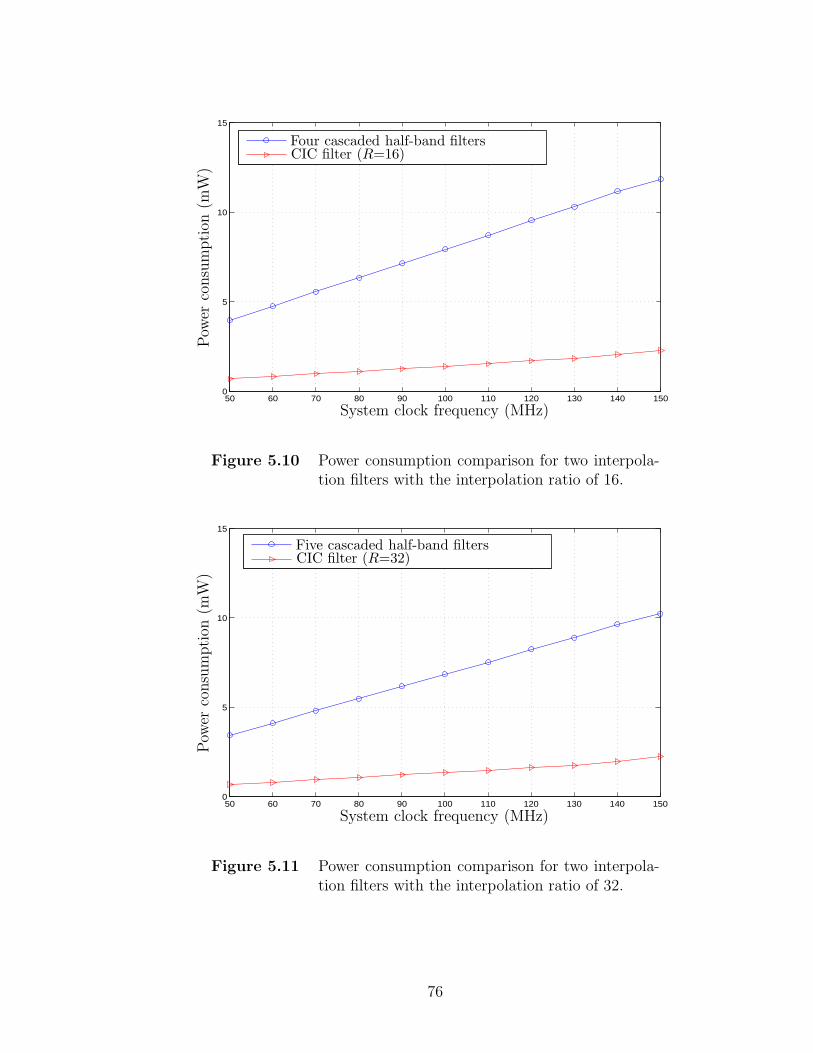
50 60 70 80 90 100 110 120 130 140 1500
5
10
15
System clock frequency (MHz)
Pow
erco
nsu
mpti
on(m
W)
Four cascaded half-band filtersCIC filter (R=16)
Figure 5.10 Power consumption comparison for two interpola-tion filters with the interpolation ratio of 16.
50 60 70 80 90 100 110 120 130 140 1500
5
10
15
System clock frequency (MHz)
Pow
erco
nsu
mpti
on(m
W)
Five cascaded half-band filtersCIC filter (R=32)
Figure 5.11 Power consumption comparison for two interpola-tion filters with the interpolation ratio of 32.
76

Table 5.1 Power consumption comparison of ISF using CSDmultiplication and MCSD multiplication.
System Power consumption Power consumptionclock of ISF using CSD of ISF using MCSD
frequency multiplications multiplications(MHz) (mW) (mW)
50 2.795 2.785
60 3.353 3.335
70 3.916 3.894
80 4.479 4.454
90 5.044 5.016
100 5.598 5.567
110 6.103 6.072
120 6.691 6.657
130 7.224 7.188
140 7.867 7.828
150 8.385 8.342
rate change factor or precompensating it by configuring SQRC coefficient memory.
Disadvantage of the precompensating method is that it will affect the frequency
response of the SQRC filter.
5.5 Performance of inverse sinc filter
As described in Section 4.5.1, the inverse sinc filter can be implemented with
two multiplication methods, CSD multiplication and MCSD multiplication. The
power consumption of these two implementations are compared in Table 5.1. The
results show that less power consumption can be achieved when the MCSD mul-
tiplication method is used in the filter. Synthesis results also show that this filter
implemented with the MCSD multiplication results in smaller area compared with
the implementation with CSD multiplication.
5.6 Summary
High level power estimation technique for IC design is introduced in this chap-
ter. Using the high level power estimation technique, different design choices are
compared for power consumption. The performance comparison shows that the pro-
77
posed QDDS architecture can save up to 60% of power consumption at 150 MHz
compared with one conventional design which just uses quarter-wave symmetry
characteristic. The power consumption comparisons for other key blocks show that
using two pulse shaping filters for I/Q processing, CIC interpolation structure and
inverse sinc filter with MCSD multiplication consume less power than alternative
design choices. These blocks with less power consumption will be integrated to
achieve a low-power modulator.
78
Chapter 6
System Integration
The performance evaluation results show that the proposed QDDS, the two
pulse shaping filters for I/Q processing, the CIC interpolation structure, and the
inverse sinc filter with MCSD multiplication consume less power than alternative
design choices. A low-power consumption modulator is implemented with these
low-power consumption blocks. This chapter describes functional verification and
power estimation of the designed modulator.
6.1 Functional verification
6.1.1 Testing model
In order to perform functional verification for the designed modulator, a testing
model is developed. Referring to Figure 6.1, random binary data are generated in
Matlab and saved in a testing data file. These data are used as the input for the
designed modulator. Final output data of the modulator as well as the intermediate
output data from each block are dumped into individual data files. Matlab is then
used to analyze these data files with fast fourier transform (FFT) to verify the
functionality. The coefficients of the SQRC filter, the interpolation ratio of the CIC
filter and the digital tuning word of the QDDS must be configured before testing.
For testing purpose, the coefficient data for the SQRC filter is configured with
the impulse response shown in Figure 4.10, i.e., the roll-off factor is 0.22. All the
spectrums shown in this chapter are based on this same roll-off factor for SQRC
filter. Since the configuration of the roll-off factor only controls the transmitting
signal’s bandwidth, the output spectrum purity won’t be affected by this configu-
79

Random binary data
generated in Matlab
Testing data file
Digital modulator
under test
Analysis of the final
output
Configurations of the
coefficients of the SQRC
filter, the CIC filters and
the QDDS
Analysis of
intermediate results :
outputs from SQRC filter,
CIC filters and QDDS
Figure 6.1 Testing model.
ration.
6.1.2 QDDS
The outputs of the QDDS are the first intermediate results to be verified. As
described in Equation (2.1), the QDDS output frequency is controlled by the digital
tuning word. Four tuning words are used to test the QDDS. These tuning words
are 0X1999999A, 0X1AA00000, 0X26666666 and 0X66666666. The corresponding
output frequencies for the tuning words are about 0.1 × frefclk, 0.104 × frefclk,
0.15 × frefclk and 0.45 × frefclk, respectively. The spectrums for four tuning words
are shown in Figure 6.2.
As one can see from the output spectrum, the largest spur for sub-figure fout ≈0.1× frefclk is about 62 dB lower than the expected output signal, the largest spur
for sub-figure fout ≈ 0.104 × frefclk is about 70 dB lower than the expected output
signal, the largest spur for sub-figure fout ≈ 0.15×frefclk is about 64 dB lower than
80
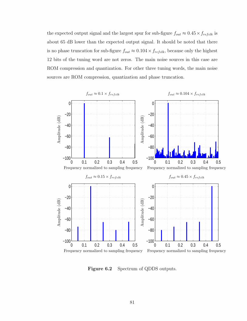
the expected output signal and the largest spur for sub-figure fout ≈ 0.45×frefclk is
about 65 dB lower than the expected output signal. It should be noted that there
is no phase truncation for sub-figure fout ≈ 0.104× frefclk, because only the highest
12 bits of the tuning word are not zeros. The main noise sources in this case are
ROM compression and quantization. For other three tuning words, the main noise
sources are ROM compression, quantization and phase truncation.
0 0.1 0.2 0.3 0.4 0.5−100
−80
−60
−40
−20
0
0 0.1 0.2 0.3 0.4 0.5−100
−80
−60
−40
−20
0
0 0.1 0.2 0.3 0.4 0.5−100
−80
−60
−40
−20
0
0 0.1 0.2 0.3 0.4 0.5−100
−80
−60
−40
−20
0
Frequency normalized to sampling frequencyFrequency normalized to sampling frequency
Frequency normalized to sampling frequencyFrequency normalized to sampling frequency
Am
plitu
de
(dB
)
Am
plitu
de
(dB
)
Am
plitu
de
(dB
)
Am
plitu
de
(dB
)
fout ≈ 0.1 × frefclk fout ≈ 0.104 × frefclk
fout ≈ 0.15 × frefclk fout ≈ 0.45 × frefclk
Figure 6.2 Spectrum of QDDS outputs.
81
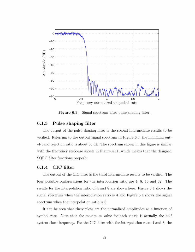
0 0.5 1 1.5 2−80
−70
−60
−50
−40
−30
−20
−10
0
Frequency normalized to symbol rate
Am
plitu
de
(dB
)
Figure 6.3 Signal spectrum after pulse shaping filter.
6.1.3 Pulse shaping filter
The output of the pulse shaping filter is the second intermediate results to be
verified. Referring to the output signal spectrum in Figure 6.3, the minimum out-
of-band rejection ratio is about 55 dB. The spectrum shown in this figure is similar
with the frequency response shown in Figure 4.11, which means that the designed
SQRC filter functions properly.
6.1.4 CIC filter
The output of the CIC filter is the third intermediate results to be verified. The
four possible configurations for the interpolation ratio are 4, 8, 16 and 32. The
results for the interpolation ratio of 4 and 8 are shown here. Figure 6.4 shows the
signal spectrum when the interpolation ratio is 4 and Figure 6.4 shows the signal
spectrum when the interpolation ratio is 8.
It can be seen that these plots are the normalized amplitudes as a function of
symbol rate. Note that the maximum value for each x-axis is actually the half
system clock frequency. For the CIC filter with the interpolation rates 4 and 8, the
82
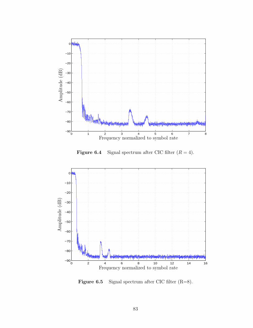
0 1 2 3 4 5 6 7 8−90
−80
−70
−60
−50
−40
−30
−20
−10
0
Frequency normalized to symbol rate
Am
plitu
de
(dB
)
Figure 6.4 Signal spectrum after CIC filter (R = 4).
0 2 4 6 8 10 12 14 16−90
−80
−70
−60
−50
−40
−30
−20
−10
0
Frequency normalized to symbol rate
Am
plitu
de
(dB
)
Figure 6.5 Signal spectrum after CIC filter (R=8).
83

maximum value is 8×symbol rate and 16×symbol rate respectively. The frequency
is normalized to the symbol rate instead of the system clock frequency for better
demonstration of the position of the residual spectrum. For example, when the CIC
filter is configured with the interpolation ratio of 4, there are 3 unwanted images
located at 4×symbol rate, 8×symbol rate and 12×symbol rate. One can clearly see
the residual spectrum at 4×symbol rate and a small residual spectrum at 8×symbol
rate in Figure 6.4. The other residual spectrum at 12×symbol rate is symmetrical
with the residual spectrum at 4×symbol rate about half system clock frequency.
One can also compare Figure 6.4 with Figure 4.14, and compare Figure 6.5 with
Figure 4.15. The spectrum shown in Figure 6.4 and Figure 6.5 are almost identical
to the periodic spectrum times the corresponding frequency response of the CIC
filter. This means that the designed CIC filter is working properly.
6.1.5 Modulator
Since both the interpolation ratio of the CIC filter and the output frequency of
the QDDS are configurable, there are a number of possible configurations. Only a
selected testing results are shown here. Note that all the results are obtained with
the inverse sinc filter turned on.
Figure 6.6 shows the results with tuning word of 0X1999999A and four possible
interpolation ratios. The corresponding output center frequency is about 0.1 ×frefclk. There are two images at about 0.3 × frefclk and 0.5 × frefclk in Figure 6.6.
By comparing this figure with the spectrum plot for fout ≈ 0.1 × frefclk in Figure
6.2, one can understand that the images at about 0.3 × frefclk and 0.5 × frefclk are
resulted from the multiplication of the baseband signal with the spurs of the QDDS.
Figure 6.7 shows the results with tuning word of 0X1AA00000 and four possible
interpolation ratios. The corresponding output center frequency is about 0.104 ×frefclk. There are also two small images at about 0.314 × frefclk and 0.48 × frefclk
shown in Figure 6.7. For the same reason that the baseband signal is multiplied
with the big spurs of the QDDS in Figure 6.2.
84
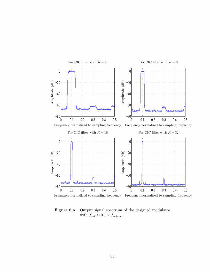
0 0.1 0.2 0.3 0.4 0.5−80
−60
−40
−20
0
0 0.1 0.2 0.3 0.4 0.5−80
−60
−40
−20
0
0 0.1 0.2 0.3 0.4 0.5−80
−60
−40
−20
0
0 0.1 0.2 0.3 0.4 0.5−80
−60
−40
−20
0
Frequency normalized to sampling frequencyFrequency normalized to sampling frequency
Frequency normalized to sampling frequencyFrequency normalized to sampling frequencyA
mplitu
de
(dB
)
Am
plitu
de
(dB
)
Am
plitu
de
(dB
)
Am
plitu
de
(dB
)
For CIC filter with R = 4 For CIC filter with R = 8
For CIC filter with R = 16 For CIC filter with R = 32
Figure 6.6 Output signal spectrum of the designed modulatorwith fout ≈ 0.1 × frefclk.
85

0 0.1 0.2 0.3 0.4 0.5−80
−60
−40
−20
0
0 0.1 0.2 0.3 0.4 0.5−80
−60
−40
−20
0
0 0.1 0.2 0.3 0.4 0.5−80
−60
−40
−20
0
0 0.1 0.2 0.3 0.4 0.5−80
−60
−40
−20
0
Frequency normalized to sampling frequencyFrequency normalized to sampling frequency
Frequency normalized to sampling frequencyFrequency normalized to sampling frequencyA
mplitu
de
(dB
)
Am
plitu
de
(dB
)
Am
plitu
de
(dB
)
Am
plitu
de
(dB
)
For CIC filter with R = 4 For CIC filter with R = 8
For CIC filter with R = 16 For CIC filter with R = 32
Figure 6.7 Output signal spectrum of the designed modulatorwith fout ≈ 0.104 × frefclk.
86

50 60 70 80 90 100 110 120 130 140 1508
10
12
14
16
18
20
22
24
26
System clock frequency (MHz)
Pow
erco
nsu
mpti
on(m
W)
Figure 6.8 Power consumption estimation of the designed mod-ulator after logic synthesis.
6.2 Power consumption estimation
6.2.1 Power consumption estimation after logic synthesis
The power consumption of the designed modulator is estimated in logic synthe-
sizer first. The power consumption estimated at this stage is the core power of a
chip [28]. It is estimated under the following conditions: interpolation ratio of the
CIC filter is 4; the inverse sinc filter is turned on; the switching activity for the input
port is set at 0.25; and the wire-load values are chosen to be worst case wire-load
values. As shown in Figure 6.8, the core of the designed modulator consumes about
25 mW at 150 MHz system clock frequency.
6.2.2 Power consumption estimation after layout
Layout of the designed modulator is done in Cadence Encounter and the result is
shown in Figure 6.9. There are a total of 66 input/ouput pads, 5 pairs of core power
pads and 11 pairs of ring power pads. The core area is about 4.3 mm2 and the chip
area is about 7.06 mm2. With the same configuration, i.e., the interpolation ratio
of the CIC filter is 4 and the inverse sinc filter is turned on, the power consumption
87
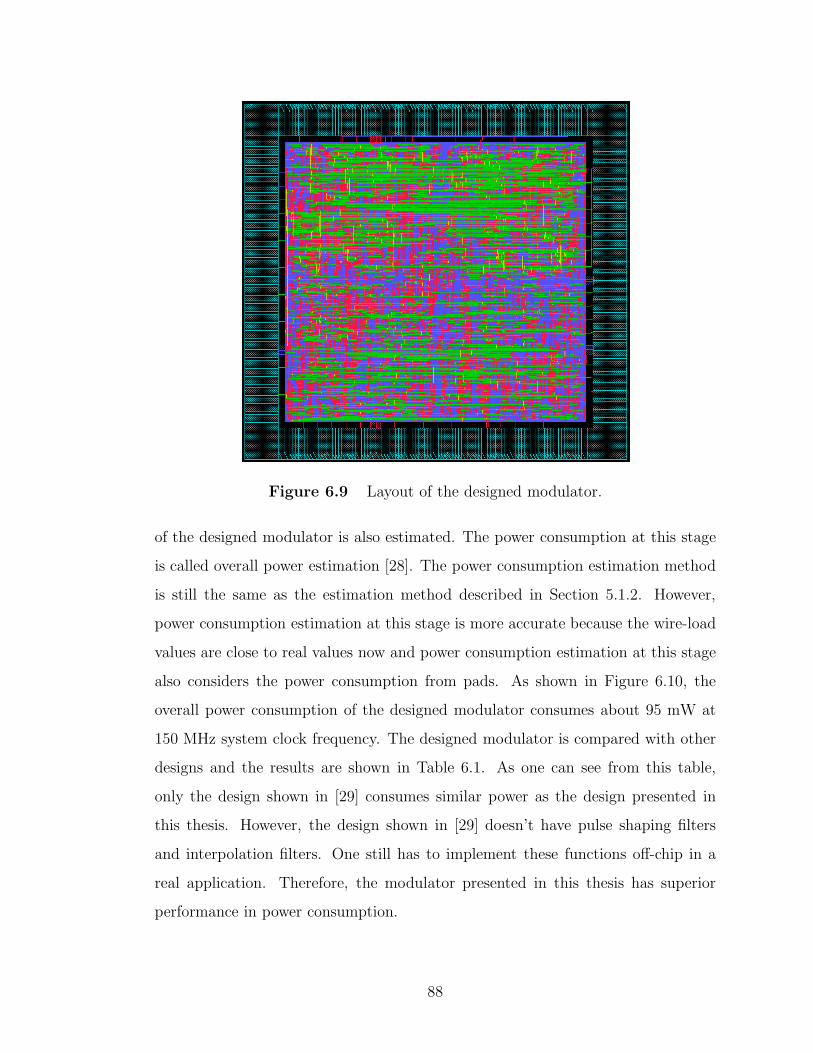
Figure 6.9 Layout of the designed modulator.
of the designed modulator is also estimated. The power consumption at this stage
is called overall power estimation [28]. The power consumption estimation method
is still the same as the estimation method described in Section 5.1.2. However,
power consumption estimation at this stage is more accurate because the wire-load
values are close to real values now and power consumption estimation at this stage
also considers the power consumption from pads. As shown in Figure 6.10, the
overall power consumption of the designed modulator consumes about 95 mW at
150 MHz system clock frequency. The designed modulator is compared with other
designs and the results are shown in Table 6.1. As one can see from this table,
only the design shown in [29] consumes similar power as the design presented in
this thesis. However, the design shown in [29] doesn’t have pulse shaping filters
and interpolation filters. One still has to implement these functions off-chip in a
real application. Therefore, the modulator presented in this thesis has superior
performance in power consumption.
88
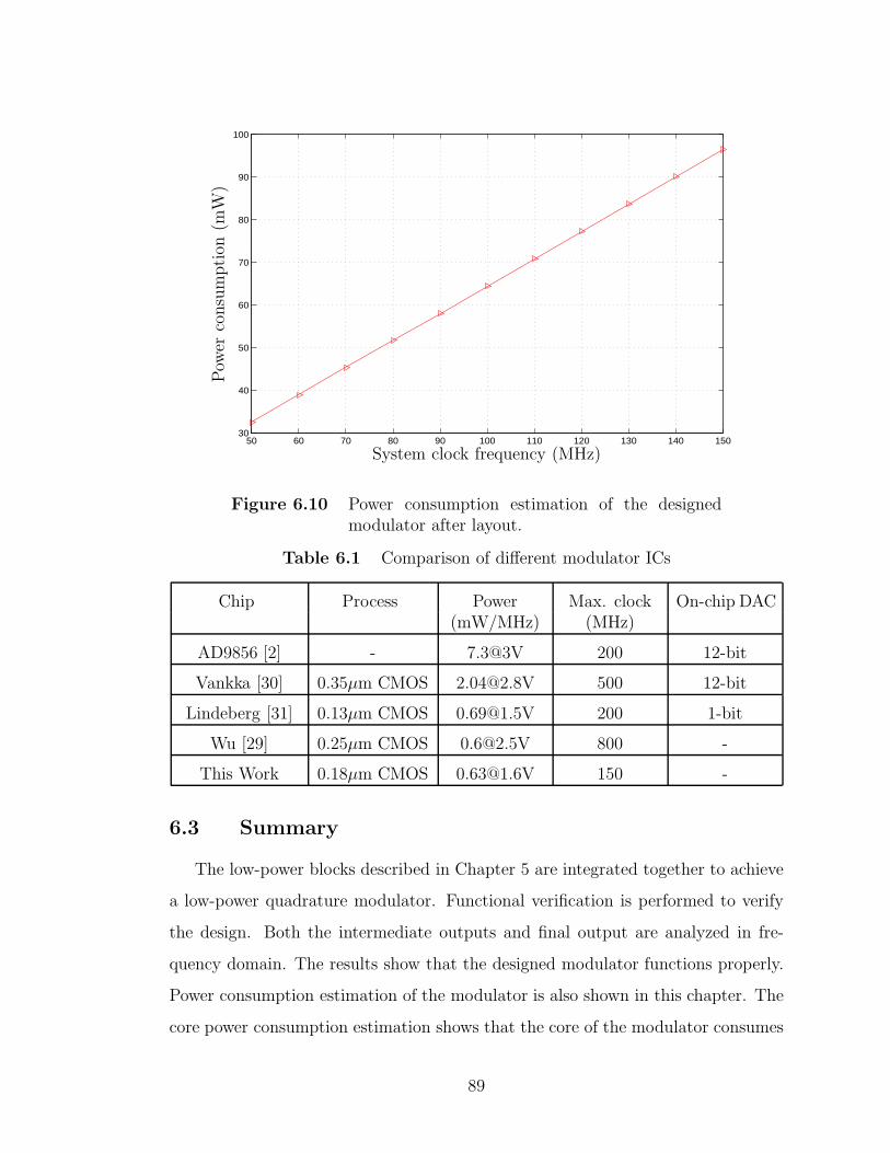
50 60 70 80 90 100 110 120 130 140 15030
40
50
60
70
80
90
100
System clock frequency (MHz)
Pow
erco
nsu
mpti
on(m
W)
Figure 6.10 Power consumption estimation of the designedmodulator after layout.
Table 6.1 Comparison of different modulator ICs
Chip Process Power Max. clock On-chip DAC(mW/MHz) (MHz)
AD9856 [2] - 7.3@3V 200 12-bit
Vankka [30] 0.35µm CMOS [email protected] 500 12-bit
Lindeberg [31] 0.13µm CMOS [email protected] 200 1-bit
Wu [29] 0.25µm CMOS [email protected] 800 -
This Work 0.18µm CMOS [email protected] 150 -
6.3 Summary
The low-power blocks described in Chapter 5 are integrated together to achieve
a low-power quadrature modulator. Functional verification is performed to verify
the design. Both the intermediate outputs and final output are analyzed in fre-
quency domain. The results show that the designed modulator functions properly.
Power consumption estimation of the modulator is also shown in this chapter. The
core power consumption estimation shows that the core of the modulator consumes
89

about 25 mW at 150 MHz system clock frequency and the overall power consump-
tion estimation shows that the modulator consumes about 95 mW at 150 MHz
system clock frequency. The designed modulator is also compared with other de-
signs and the results show that it has superior performance in power consumption.
90
Chapter 7
Conclusions
Quadrature digital modulation techniques are widely used in modern wireless
communication systems because of their high performance and flexibility. However,
these advantages come at the cost of high power consumption. For example, one
commercially used modulator [2] consumes about 1100 mW at 150 MHz. This
thesis focuses on the integrated circuit implementation of a low-power quadrature
digital modulator in 0.18µm CMOS technology which is intended to be used in a
variety of portable applications such as cell phones and personal digital assistants.
The designed quadrature digital modulator consists of several key blocks: a
QDDS, pulse shaping filters, interpolation filters and an inverse sinc filter. The
QDDS generates sine/cosine carrier reference signals for the modulator. The pulse
shaping filters are used to limit transmitting bandwidth and reduce intersymbol
interference. The interpolation filters are used to increase sampling rate and enable
the translation from baseband to intermediate frequency within digital domain.
The inverse sinc filter is used to precompensate the sinc distortion coming from the
following DAC.
The design strategy used in this modulator is trying to find low-power im-
plementation for each block inside and then integrate them together to achieve a
low-power quadrature digital modulator. In order to find low-power consumption
implementation for the key blocks, each block is implemented with multiple design
choices and high-level power estimation is used for fast comparison between these
multiple design choices. Lower power consumption blocks are integrated to achieve
a low-power modulator and performance of the designed modulator is evaluated.
91
7.1 Conclusions
Several ROM compression methods are used to reduce the ROM size for the
implementation of the QDDS. By combining Suntherland algorithm, sine-phase dif-
ference method and quad line approximation method, the final ROM compression
ratio achieved is 14.7 compared with one conventional design which simply uses
quarter-wave symmetry characteristic of sine and cosine waves. The power con-
sumption comparison shows that the proposed QDDS circuit can save up to 60%
of the power consumption at 150 MHz system clock frequency compared with the
same conventional design. Extra noises are introduced because of these compression
methods used.
The pulse shaping filter is implemented according to the polyphase structure
and the filter length is 128 with a built-in four times upsampling function. There
are two general approaches to design this filter for a quadrature modulator. The
first approach uses two pulse shaping blocks to process I and Q data separately.
The second approach just uses one pulse shaping block by interleaving I and Q
streams in time. The power consumption comparison shows that the second ap-
proach consumes more power although it is more hardware efficient. So the one
using two pulse shaping blocks is chosen as the implementation method in this
design.
Interpolation ratio of the interpolation filters in the modulator is limited to 4,
8, 16 and 32. Two hardware efficient interpolation architectures are considered in
the modulator. One is CIC filter and the other is half-band FIR filter. The power
consumption comparison shows CIC filter consumes less power than its counter-
part. So CIC interpolation structure is chosen as the interpolation structure in this
modulator. The penalty is the frequency dependant distortion coming from CIC
filter. However, one can alleviate this distortion by using higher interpolation ratio
or by configuring the coefficient RAM of pulse shaping filter with the convolution
of two impulse responses - one is the impulse response of the pulse shaping filter
and the other is the impulse response of an inverse CIC filter.
92

The inverse sinc filter is implemented with the length of 9. Since all the multipli-
cations in this filter are constant multiplications, conventional design usually uses
CSD multiplication method to implement all the multipliers. However, the MCSD
multiplication method is more suitable for ASIC design. The power consumption
estimation shows the filter using MCSD multiplication method does lead to less
power consumption and is more hardware efficient compared with the design using
CSD multiplication method.
The final quadrature digital modulator is implemented with the proposed low-
power QDDS architecture and other low-power consumption blocks which are found
by comparing power consumption of different design approaches for each block.
The results show that the modulator designed with this strategy leads to less power
consumption and provides a universal low-power solution for quadrature digital
modulator design. The power consumption estimation shows that the designed
modulator consumes about 95 mW at 150 MHz system clock frequency which is
much lower than the similar product that consumes about 1100 mW at 150 MHz
system clock frequency.
The novel 32-bit low-power QDDS in the modulator can be used in various
quadrature digital modulators and demodulators which have low-power consump-
tion requirement. The designed modulator also has a number of other features:
• 0 to 75 MHz output bandwidth
• Configurable pulse shaping filters and interpolation filters
• Internal sin(x)/x correction filter
7.2 Future work
There are still a number of interesting areas that can be investigated further in
the future.
• Circuit level low-power techniques
Most of the low-power consumption techniques used in this thesis are at system
level and algorithm level. Other low-power techniques at circuit level, such as
multiple supple voltages and dynamic supply voltage scaling can also be applied to
93

study how much power can further be saved.
• On-chip digital to analog converter
There will be several advantages if a low-power on-chip DAC can be included.
One advantage is that it can avoid delays and line loading caused by interchip
connection to an off-chip DAC. Another advantage is that it can save both power
and area.
• Multilevel QAM
The modulator structure described in this thesis can be used for many quadra-
ture digital modulation. It is interesting to apply this structure to a quadrature
modulator with low-power consumption that can support multilevel QAM.
94

References
[1] Paul Burns, Software defined radio for 3G, Artech House, 2003.
[2] AD9856 data sheet, Analog Devices.
[3] International technology roadmap for semiconductors design 2005 edition,
ITRS, 2005.
[4] A technical tutorial on digital signal synthesis, Analog Devices.
[5] Eric Salt, EE461 class notes, Department of Electrical and Computer Engi-
neering, University of Saskatchewan.
[6] W. H. Tranter, K. S. Shanmugan, T. S. Rappaport, and K. L. Kosbar, Com-
munications systems simulation with wireless applications, Prentice Hall, 2004.
[7] J. R. Barry, Edward A. Lee, and David G. Messerschmitt, Digital communi-
cations, Kluwer Academic Publishers, 3rd edition, 1988.
[8] Alan V. Oppenheim, Ronald W. Schafer, and John R. Buck, Discrete-time
signal processing, Prentice Hall, 2nd edition, 1999.
[9] Eugene B.Hogenauer, “An economical class of digital filters for decimation
and interpolation,” IEEE TRANSATION ON ACOUSTICS, SPEECH, AND
SIGNAL PROCESSING, vol. ASSP-29, no. 2, pp. 155–162, APRIL 1981.
[10] Fredric J. Harris, Multirate signal processing for communication systems, Pren-
tice Hall, 2004.
[11] Digital modulation in communications systems - an introduction, Agilent tech-
nology.
95
[12] Randall L. Geiger, Phillip E. Allen, and Noel R. Strader, VLSI design tech-
niques for analog and digital circuits, McGraw-Hill, 1990.
[13] Henry Samueli, “The design of multiplierless FIR filters for compensating
D/A converter frequency response distortion,” IEEE TRANSACTION ON
CIRCUITS AND SYSTEMS, vol. 35, no. 8, pp. 1064–1066, AUGUST 1988.
[14] Integrated circuit history, http: //en.wikipedia.org/wiki/Integrated circuit.
[15] CMC digital IC design flow tutorial, CMC Microsystems, AUGUST 2004.
[16] Scan and ATPG process guide, Mentor Graphics.
[17] Byung-do Yang, Jang-Hong Choi, Seon-Ho Han, Lee-sup Kim, and Hyun-Kyu
Yu, “An 800-MHz low-power direct digital frequency synthesizer with an on-
chip D/A converter,” IEEE JOURNAL OF SOLID-STATE CIRCUITS, vol.
39, no. 5, pp. 761–774, MAY 2004.
[18] David S. Sunderland, Roger A. Strauch, Steven S. Wharfield, and Henry T.
Peterson, “CMOS/SOS frequency synthesizer LSI circuit for spread spectrum
communications,” IEEE JOURNAL OF SOLID-STATE CIRCUITS, vol. 19,
no. 4, pp. 497–505, AUGUST 1984.
[19] H. T. Nicholas and H. Samueli, “An analysis of the output spectrum of direct
digital frequency synthesizers in the presence of phase accumulator truncation,”
Proc. 41st Annual Frequency Control Symposium, May 1987, pp. 495–502.
[20] N.J. Fliege, Multirate digital signal processing, John Wiley and Sons Inc.,
1994.
[21] K. Hwang, Computer arithemetic: principles, architecture and design, Wiley,
1979.
[22] K. Wiatr and E. Jamro, “Constant coefficient multiplication in FPGA struc-
tures,” Euromicro Conference, September 2000, vol. 1, pp. 252–259.
96

[23] Will Leavitt, Reducing gate count and power with power compiler, Emulex
Corporation, FEBRUARY 2005.
[24] Christian Piguet, Low-power CMOS circuits technology, logic design and CAD
tools, Taylor and Francis Group, 2005.
[25] Luca Benini, Alessandro Bogliolo, and Giovanni De Micheli, “A survey of de-
sign techniques for system-level dynamic power management,” IEEE TRAN-
SATION ON VERY LARGE SCALE INTEGRATION SYSTEMS, vol. 8, no.
3, pp. 299–316, JUNE 2000.
[26] DesignWare IP family reference guide, Synopsys, JUNE 2006.
[27] Xiaoying Zhao, Kui Wang, Xu Cheng, and Dong Tong, “A leakage power
estimation method for standard cell based design,” 2005 IEEE Conference on
Electron Devices and Solid-State Circuits, DECEMBER 2005, pp. 821–824.
[28] Jim Flynn, “Accurate power-analysis techniques support smart SOC-design
choices,” EDN, DECEMBER 2004, pp. 69–74.
[29] Yanlin Wu, Dengwei Fu, and Alan Willson, “A 415 MHz direct digital quadra-
ture modulator in 0.25-µm CMOS,” IEEE CUSTOM INTEGRATED CIR-
CUITS CONFERENCE, September 2003, vol. 1, pp. 287–290.
[30] J. Vankka, J. Sommarek, J. Ketola, I. Teikari, and K.A.I Halonen, “A digital
quadrature modulator with on-chip D/A converter,” IEEE JOURNAL OF
SOLID-STATE CIRCUITS, vol. 38, no. 10, pp. 1635–1642, OCTOBER 2003.
[31] Jonne Lindeberg, Jouko Vankka, Johan Sommarek, and Kari Halonen, “A 1.5-
V direct digital synthesizer with tunable delta-sigma modulator in 0.13-µm
CMOS,” IEEE JOURNAL OF SOLID-STATE CIRCUITS, vol. 40, no. 9, pp.
1978–1982, SEPTEMBER 2005.
97

Appendix A
Scripts for Digital IC Design
A.1 A script for invoking NCsim in batch mode
#!/bin/csh -f
ncvlog ./test.v
ncvlog ./testbench.v
ncelab -access +r worklib.testbench:module
ncsim -tcl worklib.testbench:module <<!
run 10000 us
quit
!
A.2 A script for invoking Synopsys Design Compiler in
batch mode
#!/bin/csh -f
dc shell <<!
analyze -format verilog -lib DEFAULT {“./test.v”}elaborate test -arch“verilog” -lib DEFAULT -update
current design = “./test.db:test”
check design
set load 10 find(port,“output”)
create clock -name “clk” -period 5 -waveform { “0” “2.5” } {“clk”}set clock skew -plus uncertainty 0.5 “clk”
98

set clock skew -minus uncertainty 0.5 “clk”
set dont touch network find( clock, “clk”)
set fix multiple port nets -all
compile -ungroup all
compile -map effort high -incremental map
report area > ./test.rpt
report power >> ./test.rpt
report timing -path full -delay max -max paths 1 -nworst 1 >> ./test.rpt
write -format verilog -hierarchy -output “./test gate.v” {“./test.db:test”}quit
!
A.3 A script for invoking Cadence PKS in batch mode
for timing optimization
#!/bin/csh -f
pks shell <<!
read alf /CMC/kits/artisan18/FE/aci/sc/alf/fast.alf
read tlf -force /CMC/kits/artisan18/FE/.../tpz973gbc.tlf
read lef /CMC/kits/artisan18/FE/aci/sc/lef/tsmc18 6lm.lef
read lef update /CMC/kits/artisan18/FE/.../tpz973g 6lm.lef
check library checklib.rpt
read verilog test ctgo.v
do build generic
read def test ctgo.def
set clock clk -period 5
set clock insertion delay 0.1 clk
set clock propagation propagated
set clock uncertainty -early 0.1
set clock root -clock
99

do route -timing driven
do fix hold -buffer -critical ratio 0.0
do place -eco
do route -timing driven
report timing > pks postholdfix.rpt
write verilog -hier test postholdfix.v
write def -hier delimiter “/” modulator postholdfix.def
exit
!
100