Embed Size (px)
Citation preview
Abstract—This paper presents a digital controller interface
for an non-volatile memory (NVM) IP [1] which is part of an embedded 8051 microprocessor system. The embedded microprocessor system is targeted to be integrated as part of a micro mirror projection ASIC for MEMS scanner control and sensing [2]. The NVM memory controller interface with the storage of NVM is used to calibrate the position of micro mirror MEMS on the fly during the projection scanning mode, and store and load the configuration parameters for ASIC module initialization during power up stage. The design has been fabricated with 0.18 µm CMOS process and measurement result proves the full function of the design concept.
Index Terms—Microcontroller, non-volatile memory (NVM), micro mirror projection, micro-electro-mechanical systems (MEMS).
I. INTRODUCTION The advancement of shrinking technology on the
semiconductor process paves the way for integration of more sophisticated electronic devices on a single die. This trend still keeps track with Moore’s law with integration density doubling every eighteen months. The technology shrinking makes it possible for the miniaturization of many traditional consumer electronics such as portable media player and micro or pico projector, etc. Micro mirror display [3] [4] has becoming increasingly popular in recent years due to the advancement of MEMS and CMOS technology and the exploration of new portable devices and their applications. Due to the difference of process variation between MEMS and CMOS technology, most of the MEMS devices need to be controlled and calibrated by ASIC devices based on today’s mature CMOS technology before shipped to the end consumer [5] [6]. Traditional calibration process is labor and time intensive and lack of automation. Thus the need of designing a digital controller interface for NVM to store and auto-load of pre-calibration value onto the MEMS control ASICs is highly sought for.
II. DESIGN
A. System Architecture The Micro mirror projector consists of three parts: MEMS
micro mirror, MEMS controller ASIC and laser module, of
Manuscript received August 27, 2012; revised September 27, 2012. Jianwen Luo, Peng Li, Ravinder Pal Singh and Minkyu Je are with
Institute of Microelectronics, A*STAR (Agency for Science, Technology and Research), Singapore (e-mail: [email protected]).
Tal Langer is with Maradin Ltd., 2 HaCarmel St. Yokneam 20692, Israel (e-mail: [email protected]).
which the first two parts are fabricated separately and packaged together as a single module with system in package or SiP [7]. The main goal of this project is to design and fabricate the micro mirror controller ASIC to control and sense the micro mirror’s position and to synchronize the movement of micro mirror with projection video bit stream. The micro mirror MEMS is resonating at 10KHz resonating frequency in horizontal direction by applying alternated high voltage pulse at opposite capacitor plates of the electro-static actuator, which projects the incident laser beam at horizontal position [8]. By applying saw tooth signal with synchronized timing from video stream at coils of motor located at the base plate of MEMS, the scanning mirror is able to move at the vertical direction under the motor drive, thus the projection of 2D image is realized. In this project, the SVGA [9] resolution has been achieved.
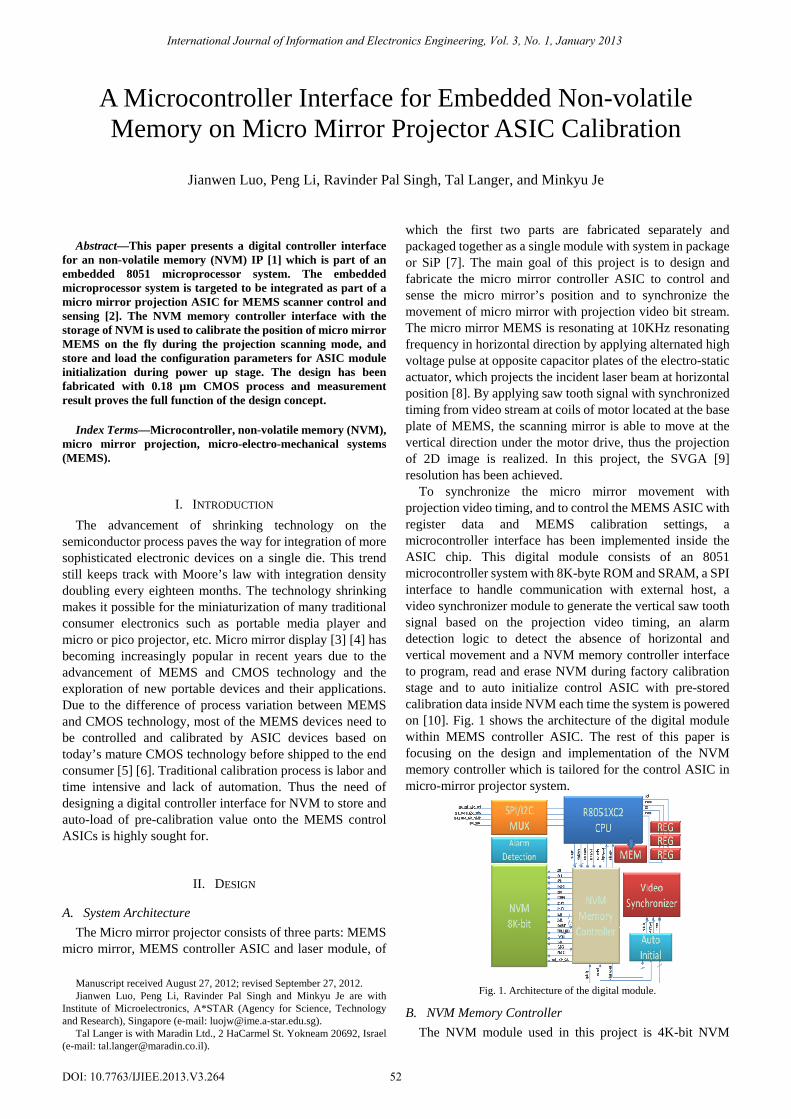
To synchronize the micro mirror movement with projection video timing, and to control the MEMS ASIC with register data and MEMS calibration settings, a microcontroller interface has been implemented inside the ASIC chip. This digital module consists of an 8051 microcontroller system with 8K-byte ROM and SRAM, a SPI interface to handle communication with external host, a video synchronizer module to generate the vertical saw tooth signal based on the projection video timing, an alarm detection logic to detect the absence of horizontal and vertical movement and a NVM memory controller interface to program, read and erase NVM during factory calibration stage and to auto initialize control ASIC with pre-stored calibration data inside NVM each time the system is powered on [10]. Fig. 1 shows the architecture of the digital module within MEMS controller ASIC. The rest of this paper is focusing on the design and implementation of the NVM memory controller which is tailored for the control ASIC in micro-mirror projector system.
Fig. 1. Architecture of the digital module.
B. NVM Memory Controller The NVM module used in this project is 4K-bit NVM
A Microcontroller Interface for Embedded Non-volatile Memory on Micro Mirror Projector ASIC Calibration
Jianwen Luo, Peng Li, Ravinder Pal Singh, Tal Langer, and Minkyu Je
DOI: 10.7763/IJIEE.2013.V3.264
International Journal of Information and Electronics Engineering, Vol. 3, No. 1, January 2013
52
fabricated in 0.18µm high voltage CMOS process. The memory controller is designed to cascade two of this 4K-bit NVM module and a charge pump (CP) to realize total 8K-bit storage. There are two kinds of data need to be stored in the NVM: the ASIC calibration data, the 600 projection row height. The calibration data is to set the control parameter of ASIC such as PLL clock phase control and filter coefficients, and is pre-loaded onto the SPI registers when power on. The projection row height of each row is to be calibrated and stored inside the NVM during calibration stage and read out during projection time. The tasks of NVM memory controller are summarized as below:
• NVM memory program. • NVM memory read. • NVM memory erase. • NVM memory and CP trimming register setting. • NVM memory and CP test register setting. • ASIC auto initialization from NVM when system
powers on. • NVM data pre-load for row height when projecting
images. • NVM program/erase verification.
To realize these tasks and interface with the on chip 8051 microcontroller, a finite state machine has been implemented inside the NVM memory controller with parameterisable settings to meet the NVM module specification. This hierarchical design enables the operational transparency to the external host. The NVM is accessible by external host through SPI commands. By mapping the NVM address to the 8051 microcontroller memory address, the access of NVM has no difference with accessing other part of microcontroller SRAM from external controller’s view. The NVM memory controller takes care of all the command encoding and generates the appropriate control signals with timing requirement to meet the NVM module specification when address mapping is pointing to NVM address.
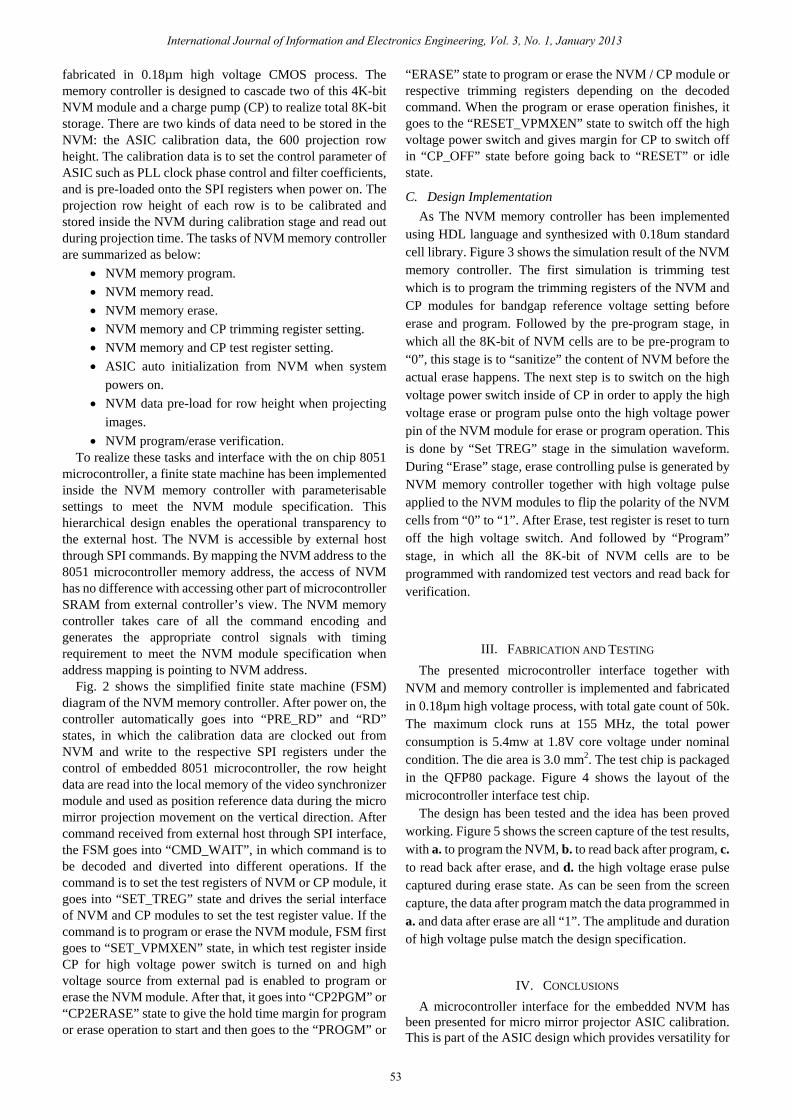
Fig. 2 shows the simplified finite state machine (FSM) diagram of the NVM memory controller. After power on, the controller automatically goes into “PRE_RD” and “RD” states, in which the calibration data are clocked out from NVM and write to the respective SPI registers under the control of embedded 8051 microcontroller, the row height data are read into the local memory of the video synchronizer module and used as position reference data during the micro mirror projection movement on the vertical direction. After command received from external host through SPI interface, the FSM goes into “CMD_WAIT”, in which command is to be decoded and diverted into different operations. If the command is to set the test registers of NVM or CP module, it goes into “SET_TREG” state and drives the serial interface of NVM and CP modules to set the test register value. If the command is to program or erase the NVM module, FSM first goes to “SET_VPMXEN” state, in which test register inside CP for high voltage power switch is turned on and high voltage source from external pad is enabled to program or erase the NVM module. After that, it goes into “CP2PGM” or “CP2ERASE” state to give the hold time margin for program or erase operation to start and then goes to the “PROGM” or
“ERASE” state to program or erase the NVM / CP module or respective trimming registers depending on the decoded command. When the program or erase operation finishes, it goes to the “RESET_VPMXEN” state to switch off the high voltage power switch and gives margin for CP to switch off in “CP_OFF” state before going back to “RESET” or idle state.
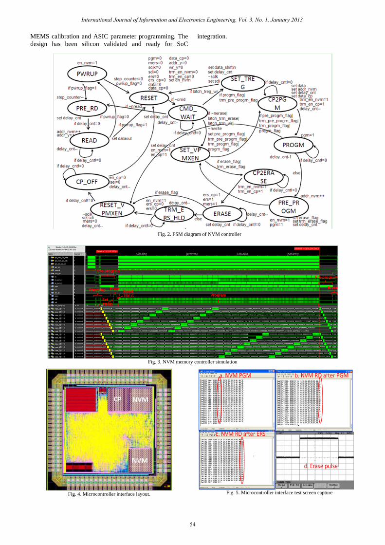
C. Design Implementation As The NVM memory controller has been implemented
using HDL language and synthesized with 0.18um standard cell library. Figure 3 shows the simulation result of the NVM memory controller. The first simulation is trimming test which is to program the trimming registers of the NVM and CP modules for bandgap reference voltage setting before erase and program. Followed by the pre-program stage, in which all the 8K-bit of NVM cells are to be pre-program to “0”, this stage is to “sanitize” the content of NVM before the actual erase happens. The next step is to switch on the high voltage power switch inside of CP in order to apply the high voltage erase or program pulse onto the high voltage power pin of the NVM module for erase or program operation. This is done by “Set TREG” stage in the simulation waveform. During “Erase” stage, erase controlling pulse is generated by NVM memory controller together with high voltage pulse applied to the NVM modules to flip the polarity of the NVM cells from “0” to “1”. After Erase, test register is reset to turn off the high voltage switch. And followed by “Program” stage, in which all the 8K-bit of NVM cells are to be programmed with randomized test vectors and read back for verification.
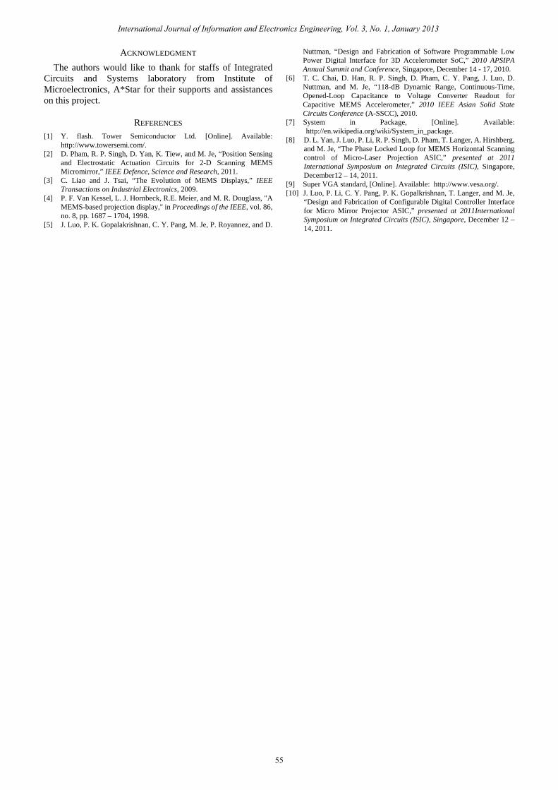
III. FABRICATION AND TESTING The presented microcontroller interface together with
NVM and memory controller is implemented and fabricated in 0.18µm high voltage process, with total gate count of 50k. The maximum clock runs at 155 MHz, the total power consumption is 5.4mw at 1.8V core voltage under nominal condition. The die area is 3.0 mm2. The test chip is packaged in the QFP80 package. Figure 4 shows the layout of the microcontroller interface test chip.
The design has been tested and the idea has been proved working. Figure 5 shows the screen capture of the test results, with a. to program the NVM, b. to read back after program, c. to read back after erase, and d. the high voltage erase pulse captured during erase state. As can be seen from the screen capture, the data after program match the data programmed in a. and data after erase are all “1”. The amplitude and duration of high voltage pulse match the design specification.
IV. CONCLUSIONS A microcontroller interface for the embedded NVM has
been presented for micro mirror projector ASIC calibration. This is part of the ASIC design which provides versatility for
International Journal of Information and Electronics Engineering, Vol. 3, No. 1, January 2013
53
MEMS calibration and ASIC parameter programming. The design has been silicon validated and ready for SoC
integration.
Fig. 2. FSM diagram of NVM controller
Fig. 3. NVM memory controller simulation
Fig. 4. Microcontroller interface layout.
Fig. 5. Microcontroller interface test screen capture
International Journal of Information and Electronics Engineering, Vol. 3, No. 1, January 2013
54
ACKNOWLEDGMENT The authors would like to thank for staffs of Integrated
Circuits and Systems laboratory from Institute of Microelectronics, A*Star for their supports and assistances on this project.
REFERENCES [1] Y. flash. Tower Semiconductor Ltd. [Online]. Available:
http://www.towersemi.com/. [2] D. Pham, R. P. Singh, D. Yan, K. Tiew, and M. Je, “Position Sensing
and Electrostatic Actuation Circuits for 2-D Scanning MEMS Micromirror,” IEEE Defence, Science and Research, 2011.
[3] C. Liao and J. Tsai, “The Evolution of MEMS Displays,” IEEE Transactions on Industrial Electronics, 2009.
[4] P. F. Van Kessel, L. J. Hornbeck, R.E. Meier, and M. R. Douglass, "A MEMS-based projection display," in Proceedings of the IEEE, vol. 86, no. 8, pp. 1687 – 1704, 1998.
[5] J. Luo, P. K. Gopalakrishnan, C. Y. Pang, M. Je, P. Royannez, and D.
Nuttman, “Design and Fabrication of Software Programmable Low Power Digital Interface for 3D Accelerometer SoC,” 2010 APSIPA Annual Summit and Conference, Singapore, December 14 - 17, 2010.
[6] T. C. Chai, D. Han, R. P. Singh, D. Pham, C. Y. Pang, J. Luo, D. Nuttman, and M. Je, “118-dB Dynamic Range, Continuous-Time, Opened-Loop Capacitance to Voltage Converter Readout for Capacitive MEMS Accelerometer,” 2010 IEEE Asian Solid State Circuits Conference (A-SSCC), 2010.
[7] System in Package, [Online]. Available: http://en.wikipedia.org/wiki/System_in_package.
[8] D. L. Yan, J. Luo, P. Li, R. P. Singh, D. Pham, T. Langer, A. Hirshberg, and M. Je, “The Phase Locked Loop for MEMS Horizontal Scanning control of Micro-Laser Projection ASIC,” presented at 2011 International Symposium on Integrated Circuits (ISIC), Singapore, December12 – 14, 2011.
[9] Super VGA standard, [Online]. Available: http://www.vesa.org/. [10] J. Luo, P. Li, C. Y. Pang, P. K. Gopalkrishnan, T. Langer, and M. Je,
“Design and Fabrication of Configurable Digital Controller Interface for Micro Mirror Projector ASIC,” presented at 2011International Symposium on Integrated Circuits (ISIC), Singapore, December 12 – 14, 2011.
International Journal of Information and Electronics Engineering, Vol. 3, No. 1, January 2013
55