Embed Size (px)
Citation preview
JOURNAL OF MICROELECTROMECHANICAL SYSTEMS, VOL. 18, NO. 3, JUNE 2009 679
A Microfabricated Planar Electrospray Array IonicLiquid Ion Source With Integrated Extractor
Blaise Gassend, Luis Fernando Velásquez-García, Akintunde Ibitayo Akinwande, and Manuel Martínez-Sánchez
Abstract—This paper reports the design, fabrication, and ex-perimental characterization of a fully microfabricated planar ar-ray of externally fed electrospray emitters that produces heavymolecular ions from the ionic liquids EMI-BF4 and EMI-Im.The microelectromechanical systems (MEMS) electrospray arrayis composed of the following two microfabricated parts: 1) anemitter die with as many as 502 emitters in 1.13 cm2 and 2) anextractor component that provides assembly alignment, electricalinsulation, and a common bias voltage to the emitter array. Thedevices were created using Pyrex and silicon substrates, as wellas microfabrication techniques such as deep reactive ion etching,low-temperature fusion bonding, and anodic bonding. The emit-ters are coated with black silicon, which acts as a wicking materialfor transporting the liquid to the emitter tips. The extractorelectrode uses a 3-D MEMS packaging technology that allowshand assembly of the two components with micrometer-level pre-cision. Experimental characterization of the MEMS electrosprayarray includes current–voltage characteristics, time-of-flight massspectrometry, beam divergence, and imprints on a collector. Thedata show that with both ionic liquids and in both polarities,the electrospray array works in the pure ionic regime, emittingions with as little as 500 V of bias voltage. The data suggestthat the MEMS electrospray array ion source could be used inapplications such as coating, printing, etching, and nanosatellitepropulsion. [2008-0270]
Index Terms—Black silicon, electrospray array, ion source,ionic liquid, 3-D packaging.
I. INTRODUCTION
E LECTROSPRAY refers to the technique of ionizing elec-trically conductive liquids using high electrostatic fields.
If an electrically conductive liquid is under the influence of anelectric field, the field will produce electrostatic pressure on thefree surface of the liquid (meniscus). The surface tension of theliquid tends to counteract the effect of the electrostatic pressure.For sufficiently small bias voltages, the perturbation of the
Manuscript received October 31, 2008; revised January 16, 2009. Firstpublished March 16, 2009; current version published June 3, 2009. Thiswork was supported in part by the Air Force Office of Scientific Research(M. Birkan, Manager), in part by the Space and Naval Warfare SystemsCenter through Award N66001-04-1-8925 (Manager R. Nguyen), and in partby the Defense Advanced Research Projects Agency (DARPA)/MicrosystemsTechnology Office and the U.S. Army Soldier Systems Center, Natick, MA,under Contract W911QY-05-1-0002 (DARPA Program Managers C. Nguyenand D. Polla and Army Program Manager H. Girolamo). The work ofB. Gassend was supported by Prof. S. Devadas. Subject Editor D. L. DeVoe.
B. Gassend was with the Department of Electrical Engineering and Com-puter Science, Massachusetts Institute of Technology, Cambridge, MA 02139USA. He is now with Exponent, Inc., Menlo Park, CA 94025 USA.
L. F. Velásquez-García, A. I. Akinwande, and M. Martínez-Sánchez arewith the Massachusetts Institute of Technology, Cambridge, MA 02139 USA(e-mail: [email protected]).
Color versions of one or more of the figures in this paper are available onlineat http://ieeexplore.ieee.org.
Digital Object Identifier 10.1109/JMEMS.2009.2015475
equilibrium shape of the meniscus remains small. If the electricfield is larger than a certain threshold, the meniscus snapsinto a conic shape called a Taylor cone [1]. The conic surfaceequilibrates the surface tension effects and the electrostaticpulling [2], i.e.,
12εoE
2n =
γ · cot[αT ]r
(1)
where En is the normal electric field acting on a point on thecone surface, εo is the permittivity of free space, γ is the surfacetension of the liquid, r is the distance between the point and thecone tip or apex, and αT is the Taylor cone semiangle. Nearthe apex, the electric field is strong enough to cause chargedparticle emission. The mechanism through which particles areemitted at the tip of the Taylor cone depends on the regime ofoperation, which is influenced by the electrical properties ofthe liquid and the flow rate. For moderately conductive liquidsand large flow rates, the cone emits a jet, which breaks up intocharged droplets [2], [3]. For liquids with high enough electricalconductivity and small enough flow rates, the electrosprayplume is composed of ions [4]. For intermediate flow ratesand electrical conductivities, a mix of ions and droplets is alsopossible [5]. Field-enhancing structures such as capillary tubesor sharp tips are used as emitters to generate the strong electricfields needed for the electrospray process and to anchor theTaylor cones [6], [7].
Numerous applications of electrospray have been reported.The most successful application for electrospray so far is asion source for mass spectrometry of large biomolecules, whichresulted in a Nobel Prize in Chemistry for J. Fenn in 2002[8]. Other applications of electrospray in the jet-emitting modeinclude fuel atomization in combustors [9], [10], nanoparticlegeneration [11], aerosol generation [12], fiber formation byelectrospinning [13] (in this case, the jet does not break upinto droplets), crop spraying [14], spray painting [15], polymercoating [16], etching [17], printing [18], and satellite propulsion[3]. There have also been several reports of electrospray devicesthat work in the ion regime, including liquid metal [19], [20]and ionic liquid ion sources [21] and more specific applica-tions such as mass-efficient nanosatellite engines [22], [23].Electrospray of ionic liquids enjoys a special interest becauseof the remarkable properties of these substances. Ionic liquidsare molten ionic salts (many of them at room temperature),composed of discrete heavy cations and anions that can beindividually customized, with tunable physical, chemical, andbiological properties [24].
The ionization of liquids using electrospray has severaladvantages compared to other approaches such as chemical
1057-7157/$25.00 © 2009 IEEE
Authorized licensed use limited to: MIT Libraries. Downloaded on February 1, 2010 at 14:03 from IEEE Xplore. Restrictions apply.
680 JOURNAL OF MICROELECTROMECHANICAL SYSTEMS, VOL. 18, NO. 3, JUNE 2009
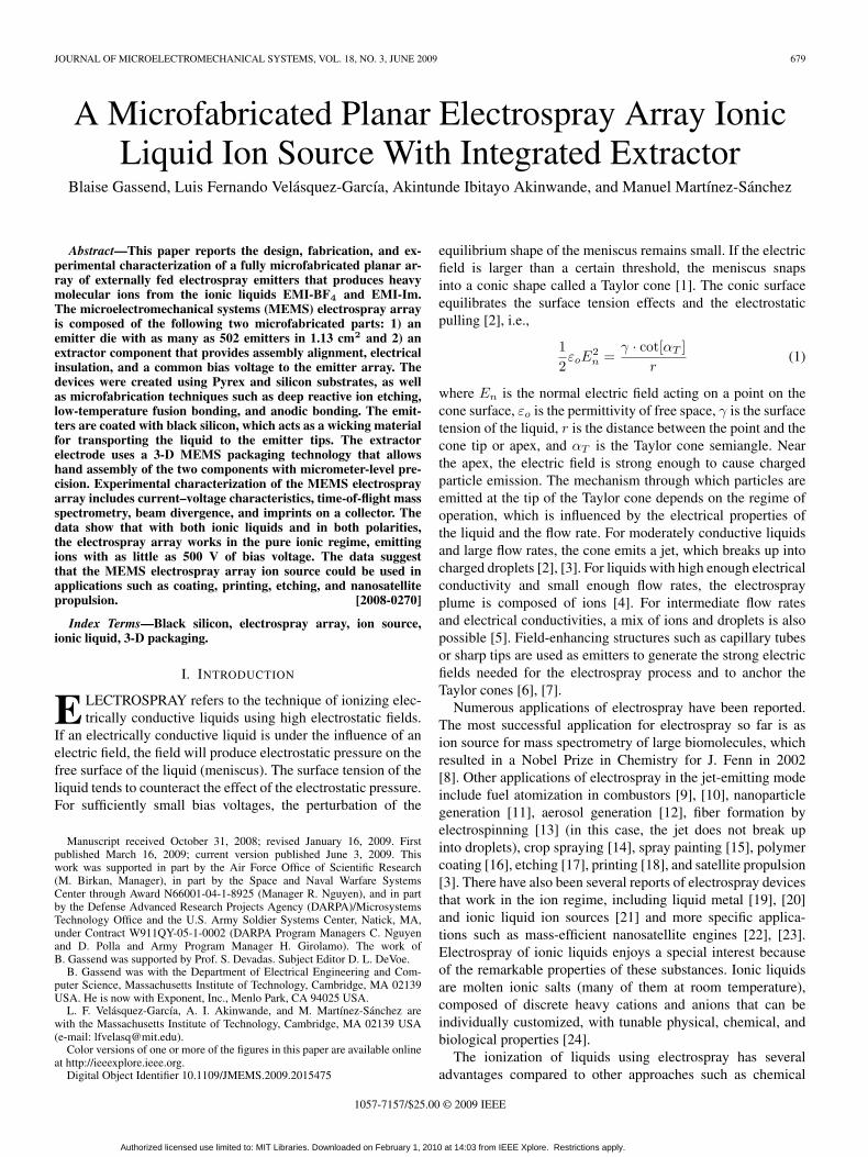
Fig. 1. (a) Microfabricated emitter array die. (b) Extractor component. (c) Backside view of an assembled electrospray array. A set of eight deflection springssurrounding the extractor interacts with the border of the emitter die to assemble the two parts with micrometer-level accuracy, and a set of four standoffs sets thevertical emitter die-to-extractor separation.
ionization and electron impact ionization. For example, whenworking in the single Taylor cone regime, the electrospray beamhas small divergence and low polydispersity [2]. Furthermore,electrospray is capable of bipolar emission [25]. Moreover,electrospray can work in a very stable fashion, deliveringrepeatable and controllable currents [3]. In addition, the electro-spray phenomenon scales favorably with a smaller emitter size.If the dimensions of the emitter are scaled down, the startupvoltage [26], [27] and the vaporization losses decrease [26].The scaling down of electrospray emitters enables batch fab-rication, which makes higher emitter packing density possiblewhile lowering the cost per emitter. In particular, plasma-basedmicrofabrication techniques can produce emitter arrays withhigh emitter uniformity [23].
Electrospray ionization poses several technical challengesfor a number of applications. First, the steady-state currentand flow rate of one emitter are rather small (usually less than0.1 μA and 10−13 m3/s, respectively), thus requiring emittermultiplexing to reach larger net currents and flow rates. Second,the implementation of multiplexed electrospray devices requireflow ballasting structures to control the emission coming fromeach emitter and achieve uniform array operation [12], [28],[29]. Third, the emitter density is controlled by the extractoraperture, the emitter-to-extractor alignment, and the emitter-to-extractor gap. Electrospray requires high electric fields tooperate, which usually implies high voltages. High voltagespose electrical insulation difficulties in microelectromechan-ical systems (MEMS)-based electrospray, including potentialshorting due to liquid flooding, and reduction of the vacuumlevel near the emitter due to the liquid vapor pressure (vacuumapplications) [26], [30]–[32].
A substantial amount of work on MEMS-based electrosprayhas been reported, covering both single- and multiple-emittersources for diverse applications such as droplet- and ion-basedspacecraft engines [23], [28], [31]–[36], droplet-based com-bustors [10], [12], and droplet-based mass spectrometry [29],[37]–[42]. This paper reports a MEMS planar array of exter-nally fed emitters with an integrated extractor electrode thatis based on previously reported work by our group [23]. Thedevice uses the ionic liquids EMI-BF4 and EMI-Im to produceions in vacuum. The choice of these liquids is motivated bytheir very low vapor pressure and their large electrical con-ductivity at room temperature [43], [44]. To the best of the
authors’ knowledge, this paper represents the first report ofa microfabricated planar electrospray array with an integratedextractor electrode that demonstrates stable operation in thepure ion emission regime. Previously reported devices werelinear arrays [28], did not have an integrated MEMS extractorelectrode [12], [23], or were not shown to emit only ions.In addition, this MEMS electrospray array uses a flexiblemodular architecture in which the emitter die is reversiblyassembled to the extractor using a system of deflection springs[45], [46]. The assembly system allows testing of a range ofquick-to-fabricate emitter dies with the same extractor com-ponent, which is the part of the device that incorporates mostof the fabrication complexity. This approach contrasts withmonolithic emitter–extractor electrospray implementations thatrequire the fabrication of a whole new device to iterate one ofits modules and that can only be inspected through destructivemeans after testing [33], [47]. Section II describes the design ofthe electrospray array ion source, while Section III elaborateson its fabrication. Finally, Section IV reports and discussesthe experimental characterization of the MEMS electrosprayarray, as well as points out potential applications of thistechnology.
II. DESCRIPTION OF THE ELECTROSPRAY ARRAY DESIGN
The MEMS electrospray array is composed of the followingtwo parts: 1) an emitter die [Fig. 1(a)] and 2) an extractor com-ponent [Fig. 1(b)]. A set of eight slender deflection springs onthe extractor component is used to align and clamp the emitterdie into place. The emitter die is about 2.1 cm in diameter,and the springs are about 1.3 cm long. The separation distancebetween the emitter die and the common extractor componentis controlled by a set of four standoffs [see Fig. 1(c) andSection II-C]. The design of the electrospray array results fromtaking into consideration issues such as the following: 1) thehydraulic impedance required for ion emission; 2) the emitterand extractor geometries needed to decrease the startup voltagewhile increasing the emitter density; 3) the structural resistanceof the extractor to electrostatic loads; and 4) the electrode-to-extractor assembly scheme to achieve low beam interceptionand electrical insulation, including electrical breakdown resis-tance against surface contamination, beam interception, andliquid flooding.
Authorized licensed use limited to: MIT Libraries. Downloaded on February 1, 2010 at 14:03 from IEEE Xplore. Restrictions apply.
GASSEND et al.: PLANAR ELECTROSPRAY ARRAY IONIC LIQUID ION SOURCE WITH INTEGRATED EXTRACTOR 681
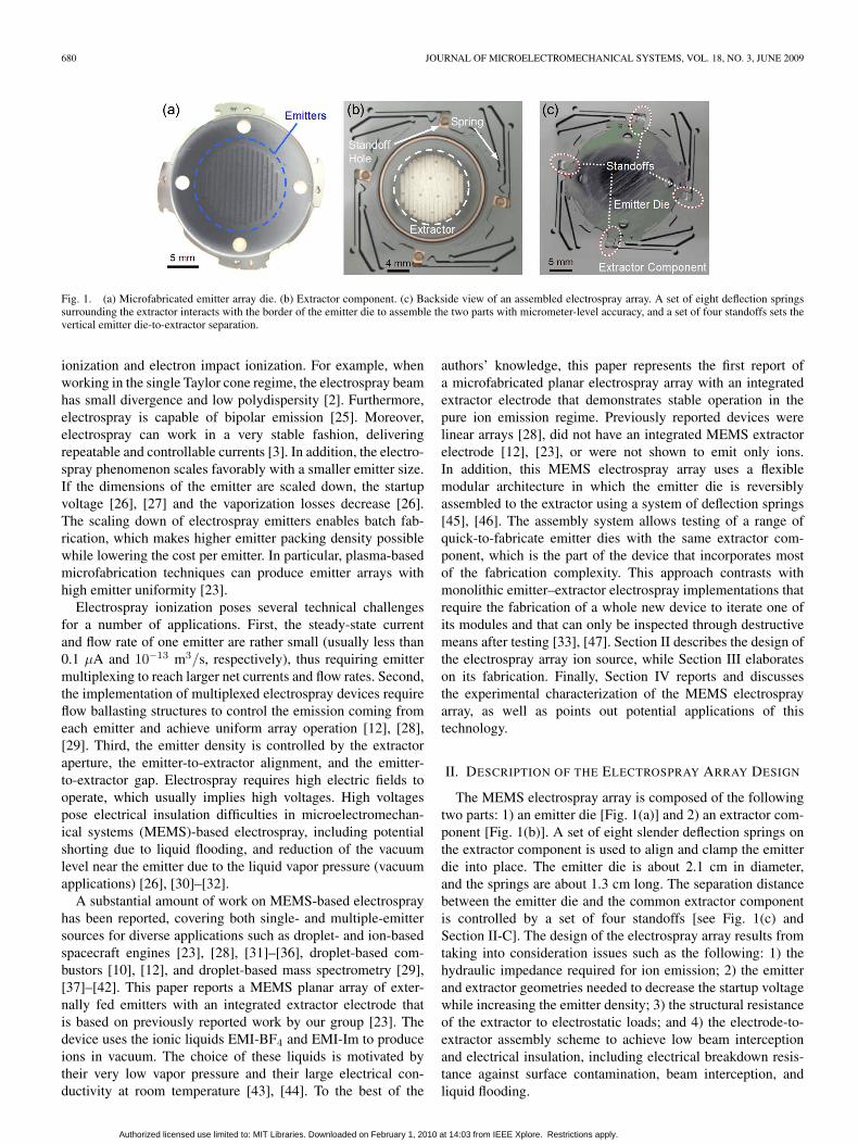
Fig. 2. (a) Cross section of the microfabricated electrospray array ion source.(b) Emitters organized in rows to increase the emitter density.
TABLE IDESCRIPTION OF THE EMITTER DIES THAT WERE BUILT
A. Emitter Die
The emitter die has an array of emitters about 400 μm tall,arranged in 13 parallel rows spaced 750 μm apart [Fig. 2(a)].The active area of the emitter die is surrounded by a raisedsupport ring [visible in Fig. 1(a)] that strengthens the emitterdie and interfaces with the spring tips in the assembly. Theemitters are organized in rows that face a common extractorslot to increase the emitter density, compared to an emitterarray where each emitter has an individual concentric extractor[Fig. 2(b)]. Three versions of the emitter die were built, withparameters described in Table I. Emitter dies with as many as502 emitters in 1.13 cm2 were fabricated. To the best of theauthors’ knowledge, this paper reports the largest and densestworking electrospray array with integrated extractor to date(4.45 emitters/mm2, almost twice the emitter density reportedby Deng et al. [10]). However, Krpoun et al. reported thefabrication of electrospray arrays with integrated extractor thathave larger emitter densities (about 18 emitters/mm2, althoughonly data from one- and two-emitter arrays were reported) [33],and our group previously reported larger and denser workingelectrospray arrays with no integrated electrode (1024 emittersin 1 cm2) [23].
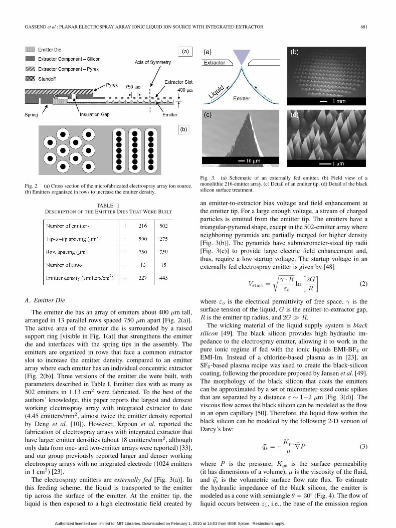
The electrospray emitters are externally fed [Fig. 3(a)]. Inthis feeding scheme, the liquid is transported to the emittertip across the surface of the emitter. At the emitter tip, theliquid is then exposed to a high electrostatic field created by
Fig. 3. (a) Schematic of an externally fed emitter. (b) Field view of amonolithic 216-emitter array. (c) Detail of an emitter tip. (d) Detail of the blacksilicon surface treatment.
an emitter-to-extractor bias voltage and field enhancement atthe emitter tip. For a large enough voltage, a stream of chargedparticles is emitted from the emitter tip. The emitters have atriangular-pyramid shape, except in the 502-emitter array whereneighboring pyramids are partially merged for higher density[Fig. 3(b)]. The pyramids have submicrometer-sized tip radii[Fig. 3(c)] to provide large electric field enhancement and,thus, require a low startup voltage. The startup voltage in anexternally fed electrospray emitter is given by [48]
Vstart =√
γ · Rεo
ln[2G
R
](2)
where εo is the electrical permittivity of free space, γ is thesurface tension of the liquid, G is the emitter-to-extractor gap,R is the emitter tip radius, and 2G � R.
The wicking material of the liquid supply system is blacksilicon [49]. The black silicon provides high hydraulic im-pedance to the electrospray emitter, allowing it to work in thepure ionic regime if fed with the ionic liquids EMI-BF4 orEMI-Im. Instead of a chlorine-based plasma as in [23], anSF6-based plasma recipe was used to create the black-siliconcoating, following the procedure proposed by Jansen et al. [49].The morphology of the black silicon that coats the emitterscan be approximated by a set of micrometer-sized conic spikesthat are separated by a distance ε ∼ 1−2 μm [Fig. 3(d)]. Theviscous flow across the black silicon can be modeled as the flowin an open capillary [50]. Therefore, the liquid flow within theblack silicon can be modeled by the following 2-D version ofDarcy’s law:
�qs = −Kps
μ�∇P (3)
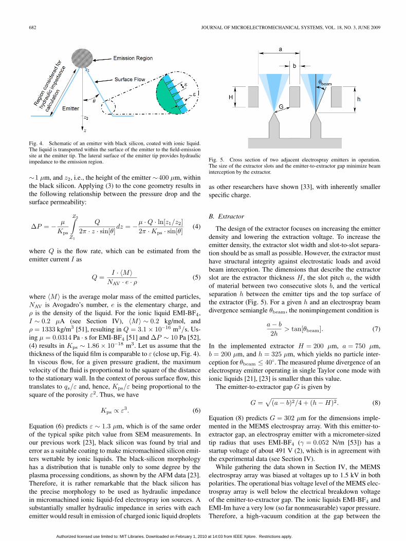
where P is the pressure, Kps is the surface permeability(it has dimensions of a volume), μ is the viscosity of the fluid,and �qs is the volumetric surface flow rate flux. To estimatethe hydraulic impedance of the black silicon, the emitter ismodeled as a cone with semiangle θ = 30◦ (Fig. 4). The flow ofliquid occurs between z1, i.e., the base of the emission region
Authorized licensed use limited to: MIT Libraries. Downloaded on February 1, 2010 at 14:03 from IEEE Xplore. Restrictions apply.
682 JOURNAL OF MICROELECTROMECHANICAL SYSTEMS, VOL. 18, NO. 3, JUNE 2009
Fig. 4. Schematic of an emitter with black silicon, coated with ionic liquid.The liquid is transported within the surface of the emitter to the field-emissionsite at the emitter tip. The lateral surface of the emitter tip provides hydraulicimpedance to the emission region.
∼1 μm, and z2, i.e., the height of the emitter ∼400 μm, withinthe black silicon. Applying (3) to the cone geometry results inthe following relationship between the pressure drop and thesurface permeability:
ΔP = − μ
Kps
Z2∫Z1
Q
2π · z · sin[θ]dz = −μ · Q · ln[z1/z2]
2π · Kps · sin[θ](4)
where Q is the flow rate, which can be estimated from theemitter current I as
Q =I · 〈M〉
NAV · e · ρ (5)
where 〈M〉 is the average molar mass of the emitted particles,NAV is Avogadro’s number, e is the elementary charge, andρ is the density of the liquid. For the ionic liquid EMI-BF4,I ∼ 0.2 μA (see Section IV), 〈M〉 ∼ 0.2 kg/mol, andρ = 1333 kg/m3 [51], resulting in Q = 3.1 × 10⁻¹⁶ m3/s. Us-ing μ = 0.0314 Pa · s for EMI-BF4 [51] and ΔP ∼ 10 Pa [52],(4) results in Kps ∼ 1.86 × 10⁻¹⁸ m3. Let us assume that thethickness of the liquid film is comparable to ε (close up, Fig. 4).In viscous flow, for a given pressure gradient, the maximumvelocity of the fluid is proportional to the square of the distanceto the stationary wall. In the context of porous surface flow, thistranslates to qs/ε and, hence, Kps/ε being proportional to thesquare of the porosity ε2. Thus, we have
Kps ∝ ε3. (6)
Equation (6) predicts ε ∼ 1.3 μm, which is of the same orderof the typical spike pitch value from SEM measurements. Inour previous work [23], black silicon was found by trial anderror as a suitable coating to make micromachined silicon emit-ters wettable by ionic liquids. The black-silicon morphologyhas a distribution that is tunable only to some degree by theplasma processing conditions, as shown by the AFM data [23].Therefore, it is rather remarkable that the black silicon hasthe precise morphology to be used as hydraulic impedancein micromachined ionic liquid-fed electrospray ion sources. Asubstantially smaller hydraulic impedance in series with eachemitter would result in emission of charged ionic liquid droplets
Fig. 5. Cross section of two adjacent electrospray emitters in operation.The size of the extractor slots and the emitter-to-extractor gap minimize beaminterception by the extractor.
as other researchers have shown [33], with inherently smallerspecific charge.
B. Extractor
The design of the extractor focuses on increasing the emitterdensity and lowering the extraction voltage. To increase theemitter density, the extractor slot width and slot-to-slot separa-tion should be as small as possible. However, the extractor musthave structural integrity against electrostatic loads and avoidbeam interception. The dimensions that describe the extractorslot are the extractor thickness H , the slot pitch a, the widthof material between two consecutive slots b, and the verticalseparation h between the emitter tips and the top surface ofthe extractor (Fig. 5). For a given h and an electrospray beamdivergence semiangle θbeam, the nonimpingement condition is
a − b
2h> tan[θbeam]. (7)
In the implemented extractor H = 200 μm, a = 750 μm,b = 200 μm, and h = 325 μm, which yields no particle inter-ception for θbeam ≤ 40◦. The measured plume divergence of anelectrospray emitter operating in single Taylor cone mode withionic liquids [21], [23] is smaller than this value.
The emitter-to-extractor gap G is given by
G =√
(a − b)2/4 + (h − H)2. (8)
Equation (8) predicts G = 302 μm for the dimensions imple-mented in the MEMS electrospray array. With this emitter-to-extractor gap, an electrospray emitter with a micrometer-sizedtip radius that uses EMI-BF4 (γ = 0.052 N/m [53]) has astartup voltage of about 491 V (2), which is in agreement withthe experimental data (see Section IV).
While gathering the data shown in Section IV, the MEMSelectrospray array was biased at voltages up to 1.5 kV in bothpolarities. The operational bias voltage level of the MEMS elec-trospray array is well below the electrical breakdown voltageof the emitter-to-extractor gap. The ionic liquids EMI-BF4 andEMI-Im have a very low (so far nonmeasurable) vapor pressure.Therefore, a high-vacuum condition at the gap between the
Authorized licensed use limited to: MIT Libraries. Downloaded on February 1, 2010 at 14:03 from IEEE Xplore. Restrictions apply.
GASSEND et al.: PLANAR ELECTROSPRAY ARRAY IONIC LIQUID ION SOURCE WITH INTEGRATED EXTRACTOR 683
tip and the extractor is expected. For a small enough productof the vacuum level and the separation gap, the electricalbreakdown of vacuum is dominated by field emission instead ofthe Townsend breakdown theory, i.e., the Paschen curve [54].In the field emission model, the ability of a sharp tip to emitelectrons at a given bias voltage depends on the workfunctionφ of the emitter material and the field-enhancing capability ofthe emitter, denoted by the field factor β [55]. The field factoris a function of geometric parameters such as the tip radii, theemitter-to-electrode gap, and the emitter-to-emitter separation.The field factor of the emitter is substantially larger than thefield factor of the extractor. Therefore, vacuum breakdown dueto field emission is only relevant when the emitter die is biasednegative to the extractor. The field factor of the emitters of theMEMS electrospray array is such that they require substantiallymore bias voltage to field emit electrons than to produce elec-trospray [55], [56].
During the operation of the MEMS electrospray array, theextractor experiences electrostatic forces that attract it to theemitter die. The following structural analysis of the extractormodels silicon as an isotropic elastic material. The choice of theextractor thickness comes from considering two effects of theelectrostatic load. First, the deflection due to the electrostaticpressure should be smaller than one third of the gap betweenthe emitter and the extractor to avoid pull-in [57]. Second, theextractor should withstand the stresses induced by the elec-trostatic load. The electrostatic pressure Pel is modeled underthe assumption that the electric field acting on the extractoris similar to the field in a parallel-plate capacitor with aninterelectrode separation of d, i.e.,
Pel =εoV
2
2d2. (9)
The deflection δ of a doubly clamped beam of length L, heightH , and Young’s modulus E under the influence of a uniformpressure PL is [58]
δ =PL · L4
32 · E · H3. (10)
The extractor is made of structural beams with spacing a andwidth b. Assuming conservatively that the electrostatic pressureis concentrated at the structural beams yields PL = (a/b)Pel.The separation between electrodes d is about h − H . Therefore,the estimated deflection of the beam is given by
δ =εo · V 2 · L4
64 · [h − H]2 · E · H3. (11)
The slots of the extractor are about 16 mm long. Using aYoung’s modulus for silicon of 145 GPa [57] and a maxi-mum voltage of 5000 V, (11) predicts that the extractor ofthe electrospray array deflects 12.5 μm, which is 10% of theundeflected emitter-to-extractor vertical separation. In termsof stress analysis, the bending stress is the dominating failurefactor. The maximum bending stress is [58]
σ =PL · L2
2H2=
a · εo · V 2 · L2
4b · [h − H]2 · H2. (12)
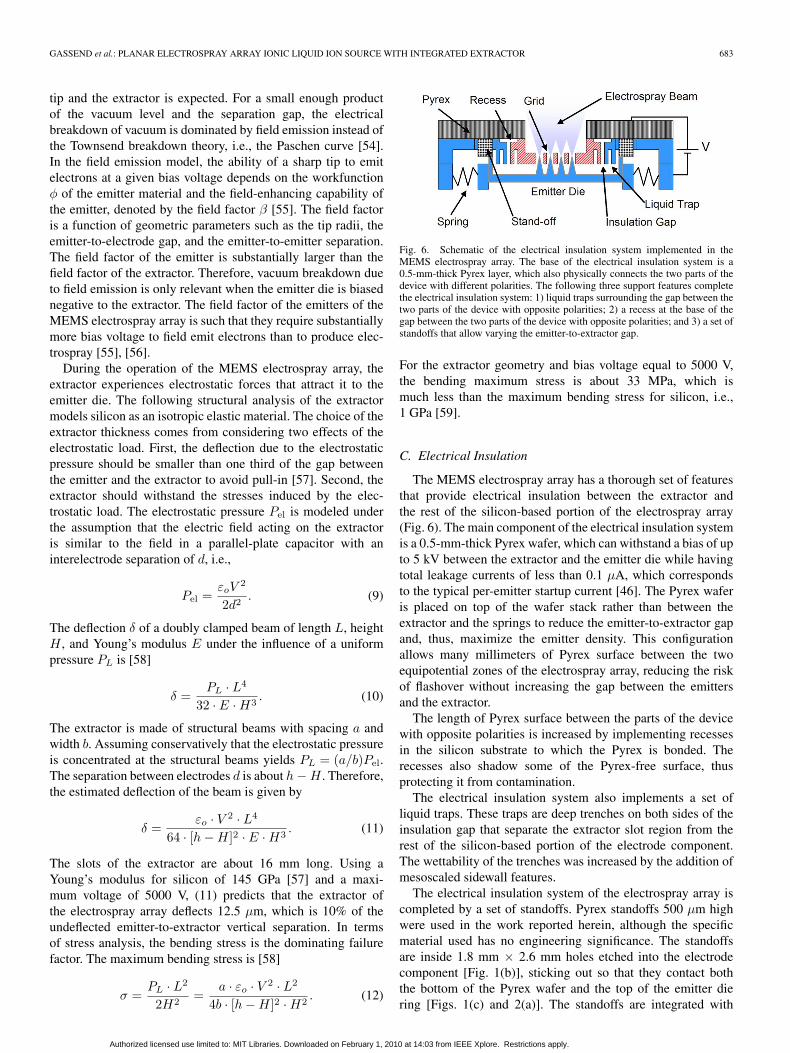
Fig. 6. Schematic of the electrical insulation system implemented in theMEMS electrospray array. The base of the electrical insulation system is a0.5-mm-thick Pyrex layer, which also physically connects the two parts of thedevice with different polarities. The following three support features completethe electrical insulation system: 1) liquid traps surrounding the gap between thetwo parts of the device with opposite polarities; 2) a recess at the base of thegap between the two parts of the device with opposite polarities; and 3) a set ofstandoffs that allow varying the emitter-to-extractor gap.
For the extractor geometry and bias voltage equal to 5000 V,the bending maximum stress is about 33 MPa, which ismuch less than the maximum bending stress for silicon, i.e.,1 GPa [59].
C. Electrical Insulation
The MEMS electrospray array has a thorough set of featuresthat provide electrical insulation between the extractor andthe rest of the silicon-based portion of the electrospray array(Fig. 6). The main component of the electrical insulation systemis a 0.5-mm-thick Pyrex wafer, which can withstand a bias of upto 5 kV between the extractor and the emitter die while havingtotal leakage currents of less than 0.1 μA, which correspondsto the typical per-emitter startup current [46]. The Pyrex waferis placed on top of the wafer stack rather than between theextractor and the springs to reduce the emitter-to-extractor gapand, thus, maximize the emitter density. This configurationallows many millimeters of Pyrex surface between the twoequipotential zones of the electrospray array, reducing the riskof flashover without increasing the gap between the emittersand the extractor.
The length of Pyrex surface between the parts of the devicewith opposite polarities is increased by implementing recessesin the silicon substrate to which the Pyrex is bonded. Therecesses also shadow some of the Pyrex-free surface, thusprotecting it from contamination.
The electrical insulation system also implements a set ofliquid traps. These traps are deep trenches on both sides of theinsulation gap that separate the extractor slot region from therest of the silicon-based portion of the electrode component.The wettability of the trenches was increased by the addition ofmesoscaled sidewall features.
The electrical insulation system of the electrospray array iscompleted by a set of standoffs. Pyrex standoffs 500 μm highwere used in the work reported herein, although the specificmaterial used has no engineering significance. The standoffsare inside 1.8 mm × 2.6 mm holes etched into the electrodecomponent [Fig. 1(b)], sticking out so that they contact boththe bottom of the Pyrex wafer and the top of the emitter diering [Figs. 1(c) and 2(a)]. The standoffs are integrated with
Authorized licensed use limited to: MIT Libraries. Downloaded on February 1, 2010 at 14:03 from IEEE Xplore. Restrictions apply.
684 JOURNAL OF MICROELECTROMECHANICAL SYSTEMS, VOL. 18, NO. 3, JUNE 2009
the rest of the device at the end of the fabrication processusing a reversible assembly procedure (see Section III-C). Thestandoffs are large enough to be handled with tweezers. Thestandoffs allow the vertical emitter-to-extractor gap to be ad-justed without modifying either of the two parts of the MEMSelectrospray array. The vertical positioning precision of thestandoffs is controlled by the height precision of the standoffsand the roughness of the contact surfaces at the top and bottomof the standoffs. The implemented standoff system providesgood vertical alignment because the standoffs are made froman anodic bondable Pyrex wafer scrap, the top surface of theemitter die ring is mirror-like fusion bondable silicon, and thebottom Pyrex surface is anodic bondable. Moreover, measure-ment of the height difference between the bottom of the emitterdie and the bottom of the electrode component in four cornersof the emitter die, using an interferometric microscope with±1 μm resolution, yielded measurements identical to within±5 μm, which is of the order of the thickness total variation ofa typical microfabrication wafer, and smaller than the variationin height between emitters.
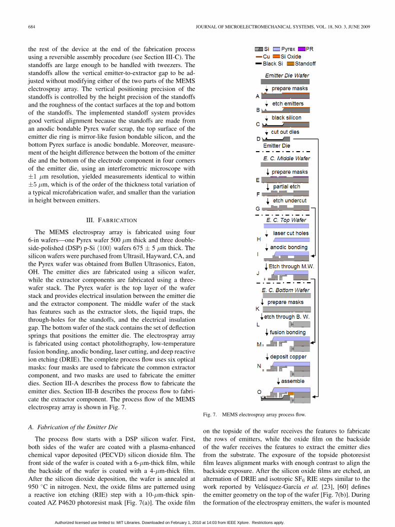
III. FABRICATION
The MEMS electrospray array is fabricated using four6-in wafers—one Pyrex wafer 500 μm thick and three double-side-polished (DSP) p-Si 〈100〉 wafers 675 ± 5 μm thick. Thesilicon wafers were purchased from Ultrasil, Hayward, CA, andthe Pyrex wafer was obtained from Bullen Ultrasonics, Eaton,OH. The emitter dies are fabricated using a silicon wafer,while the extractor components are fabricated using a three-wafer stack. The Pyrex wafer is the top layer of the waferstack and provides electrical insulation between the emitter dieand the extractor component. The middle wafer of the stackhas features such as the extractor slots, the liquid traps, thethrough-holes for the standoffs, and the electrical insulationgap. The bottom wafer of the stack contains the set of deflectionsprings that positions the emitter die. The electrospray arrayis fabricated using contact photolithography, low-temperaturefusion bonding, anodic bonding, laser cutting, and deep reactiveion etching (DRIE). The complete process flow uses six opticalmasks: four masks are used to fabricate the common extractorcomponent, and two masks are used to fabricate the emitterdies. Section III-A describes the process flow to fabricate theemitter dies. Section III-B describes the process flow to fabri-cate the extractor component. The process flow of the MEMSelectrospray array is shown in Fig. 7.
A. Fabrication of the Emitter Die
The process flow starts with a DSP silicon wafer. First,both sides of the wafer are coated with a plasma-enhancedchemical vapor deposited (PECVD) silicon dioxide film. Thefront side of the wafer is coated with a 6-μm-thick film, whilethe backside of the wafer is coated with a 4-μm-thick film.After the silicon dioxide deposition, the wafer is annealed at950 ◦C in nitrogen. Next, the oxide films are patterned usinga reactive ion etching (RIE) step with a 10-μm-thick spin-coated AZ P4620 photoresist mask [Fig. 7(a)]. The oxide film
Fig. 7. MEMS electrospray array process flow.
on the topside of the wafer receives the features to fabricatethe rows of emitters, while the oxide film on the backsideof the wafer receives the features to extract the emitter diesfrom the substrate. The exposure of the topside photoresistfilm leaves alignment marks with enough contrast to align thebackside exposure. After the silicon oxide films are etched, analternation of DRIE and isotropic SF6 RIE steps similar to thework reported by Velásquez-García et al. [23], [60] definesthe emitter geometry on the top of the wafer [Fig. 7(b)]. Duringthe formation of the electrospray emitters, the wafer is mounted
Authorized licensed use limited to: MIT Libraries. Downloaded on February 1, 2010 at 14:03 from IEEE Xplore. Restrictions apply.
GASSEND et al.: PLANAR ELECTROSPRAY ARRAY IONIC LIQUID ION SOURCE WITH INTEGRATED EXTRACTOR 685
onto a handler wafer with photoresist to avoid breakage. Afterthe emitters are etched, black silicon is formed on top of theemitters using an SF6 : O2 plasma [61] [Fig. 7(c)]. Finally,the emitter dies are cut out from the wafer backside usingDRIE. The emitter dies are kept in physical contact with thesurrounding silicon using thin tethers that are broken withtweezers when the etch is completed. Without the tethers, dieswould overheat once they were cut out from the wafer, allowingthe plasma etch to undercut the oxide mask and destroy thedie features. The dies are finally collected and dipped intoa 49% hydrofluoric acid (HF) bath to strip the oxide masks[Fig. 7(d)].
B. Fabrication of the Extractor Component
1) Middle Wafer: The process flow starts with a DSP siliconwafer. First, both sides of the wafer receive a PECVD silicondioxide film coating. The backside of the wafer receives a6-μm-thick film, while the top of the wafer receives a 3-μm-thick film. The wafer is then annealed at 950 ◦C in nitrogen.After that, both sides of the wafer are spin coated with a 10-μm-thick AZ P4620 photoresist film. The silicon oxide film onthe top of the wafer is the first layer of a two-layer nestedmask. The photoresist on the top of the wafer is exposedwith the recess features that protect the Pyrex from surfacecontamination, the through-holes for the standoffs, and theelectrical insulation gaps, as well as the features that reduce thethickness of the silicon substrate where the extractor slots areeventually etched. The exposure of the topside photoresist filmleaves aligning marks with enough contrast to align subsequentphotolithography and bonding steps. The photoresist film onthe backside of the wafer is exposed with the features of theliquid traps, the extractor slots, and the electrical insulationgaps. The layout transferred to the backside also includes aset of recesses that let the deflection springs etched on thebottom wafer move freely once the bottom and middle wafersare bonded (see Section III-B3). After the photoresist is devel-oped, the features in the photoresist are etched into the silicondioxide films using an RIE step. The photoresist films are thenstripped, and the top of the wafer is spin coated again witha 20-μm-thick AZ P4620 photoresist film. This photoresistfilm is the second layer of the two-layer nested mask. Thephotoresist film is exposed with the features of the throughholes for the standoffs, the electrical insulation gaps, and thefeatures that reduce the substrate thickness to fabricate theextractor slots. At this point, both the nested mask on top ofthe wafer and the hard mask on the bottom side are completed[Fig. 7(e)]. The top of the wafer is then etched by 450 μmusing a DRIE step to partially define the through-holes andthin out the extractor area [Fig. 7(f)]. After the DRIE step, thephotoresist is stripped using oxygen plasma, and a short 20-μm-DRIE etch step is performed to carve the insulation recesses[Fig. 7(g)].
2) Top Wafer: The Pyrex wafer is cut using a Resoneticsexcimer laser at 248 nm [Fig. 7(h)]. Before cutting the substrate,both sides of the wafer are spin coated with thick photoresistto protect the wafer surface from materials redeposited duringlaser cutting. Through-holes at the location of the extractor slot
region are etched. The wafer is then cleaned in a piranha bathto strip the protective photoresist coating.
3) Top/Middle Wafers: Once the Pyrex and the middle sili-con wafer have been processed as previously described, the twowafers are prepared for bonding. The oxide on the top of themiddle wafer is removed by quickly dipping the wafer into a49% HF bath. The silicon oxide etch rate of this bath is about2.3 μm/min. This step can be appropriately time controlledbecause of the large thickness difference between the top andbackside oxide films on the middle wafer. Alternatively, an RIEstep can be used instead of the HF dip to remove the top siliconoxide film. Once the top oxide film is stripped, a Piranha cleanis performed on both wafers. The wafers are then anodic bonded[Fig. 7(i)]. Alignment of the two wafers is done by eye becauseonly millimeter-scale precision is needed. The Pyrex/siliconwafer stack is then mounted with photoresist onto a handlerwafer, with the Pyrex side down. The silicon side of the waferstack is then etched with a DRIE step to create the insulationgap that effectively separates the extractor from the rest of thesilicon wafer. This step also etches the recesses that allow thedeflection springs to freely deflect, clears the through-holes forthe standoffs, and defines the extractor slots [Fig. 7(j)]. Once theDRIE step is completed, the wafer stack is dismounted from thehandler wafer with acetone, rinsed, and cleaned in an oxygenplasma.
4) Bottom Wafer: The process flow starts with a blank DSPsilicon wafer. First, a 0.3-μm-thick thermal oxide film is grownon the wafer to protect its bonding surfaces. The top of thewafer is then coated with a 3-μm-thick PECVD silicon oxidefilm. The substrate is then annealed at 950 ◦C in nitrogen. Next,the top of the wafer is spin coated with a 10-μm-thick AZP4620 photoresist film, which is exposed with the features ofthe deflection springs. After the photoresist is developed, thefeatures in the photoresist are etched into the silicon dioxidefilms using an RIE step [Fig. 7(k)]. Next, the springs are etchedthrough the substrate using a DRIE step [Fig. 7(l)]. During theDRIE step, the wafer is mounted onto a handler wafer to preventleakage of helium coolant. The set of springs is used in the finalassembly of the electrospray array [46].
5) Top/Middle/Bottom Wafers: The full wafer stack isbonded using a low-temperature plasma-assisted fusion bond-ing step [62], [63] because the presence of the Pyrex waferin the stack makes high-temperature annealing unfeasible. Inpreparation for bonding, the bottom wafer and the top/middlewafer stack are cleaned using a Piranha bath and then strippedof their oxide films using a 49% HF bath. The wafers are thenplaced in an RF oxygen plasma (30 s, 100 mtorr, 1 kW). Thesubstrates are then dipped in deionized water and spin dried.Finally, the substrates are aligned and pressed at room tempera-ture while applying a force of 1.2 kN [Fig. 7(m)]. The full waferstack is then heated at 400 ◦C for 2 h in a nitrogen atmospherewith no pressing. The full wafer stack is die sawed to extractthe individual common extractor components. Finally, a 1-μm-thick copper film is sputtered onto the Pyrex side of the fullwafer stack [Fig. 7(n)] using an aluminum shadow mask. Thecopper film is intended to make contact between the top surfaceof the full wafer stack and the extractor, allowing a bias voltageto be applied to the extractor.
Authorized licensed use limited to: MIT Libraries. Downloaded on February 1, 2010 at 14:03 from IEEE Xplore. Restrictions apply.
686 JOURNAL OF MICROELECTROMECHANICAL SYSTEMS, VOL. 18, NO. 3, JUNE 2009
C. Final Assembly of the MEMS Electrospray Array
The standoffs are fabricated using a die saw and a wafermade of an arbitrary material that has the desired thickness.The standoffs are inserted into their corresponding holes inthe electrode component. Then, the emitter die is twisted intoplace with a plastic tool that mates with assembly holes etchedin the emitter die. This operation makes the springs of theextractor component align and clamp the emitter die [Fig. 7(o)].Finally, pressure is applied to the die above each standoff toset the emitter-to-extractor gap. After assembly, the standoffsare held in slight compression between the emitter die and thePyrex wafer. For disassembly, tweezers are used to pry up theemitter die and the standoffs. Features have been included onthe extractor component to facilitate prying of the emitter dieby allowing easy access to its edge.
IV. EXPERIMENTAL CHARACTERIZATION
The MEMS electrospray array was tested with the ionicliquids EMI-BF4 and EMI-Im. The experimental characteriza-tion of the electrospray beam included current–voltage (I–V )characteristics, time-of-flight (TOF) mass spectrometry, beamdivergence, and imprints on a collector. The three array sizesdescribed in Table I were tested. However, this section onlyreports the data from 216- and 502-emitter arrays as theyconsistently reached steady operation after an initial overwetphase. In contrast, the one-emitter arrays never reached steadyoperation, perhaps because of particle contamination on theemitter die. In more detail, SEMs of the emitter dies occasion-ally showed particle contamination, presumably from movingthe devices between the cleanroom and the testing rig, and itis likely that some of these particles were emitting during thetests [61]. In addition, the variation in the emitter tip radiusshould significantly influence the emitter field enhancement,affecting particularly the emitter startup voltage (2). Particlecontamination and emitter tip radius variation are also presenton the larger arrays, but their impact is substantially diminishedwhen estimating per-emitter performance.
A. Electronic Instrumentation
A Keithley 6514 and a Keithley 6517A electrometers wereused for current measurements. An Agilent 54835A Infiniiumoscilloscope was used to gather waveform data and to takevoltage measurements. Pulses for the TOF experiments wereprovided by a BNC 555 pulse delay generator and were ampli-fied with a DEIPVM-4210 output pulser module, which outputspulses up to ±950 V. The emitter die voltage was suppliedby a ±5-kV Matsusada AMS-5B5, which was controlled byan Agilent 33220 A function generator. The bias voltage wasaccurate to within 20 V. In the TOF experiments, a 3.5-kVAcopian P03.5HN17 power supply was used to set the sec-ondary electron suppression grid voltage, and a +3.5-kVAcopian P03.5HP17 power supply was used for the Einzel lens.A homemade high-speed current amplifier circuit based on a TIOPA655 operational amplifier was used to measure the high-speed TOF signal. The vacuum chamber was pumped downusing two Varian TV-70 turbopumps. Finally, the chamber vac-
uum was measured using a Varian IMG-100 inverted magnetrongauge.
B. Testing Procedure
About 0.1–1 mm3 of ionic liquid was delivered to theemitter die on the black-silicon-treated surface. The liquidspread across the black-silicon surface within a few minutes,coating the emitter array. Once wetted, the emitter die wasassembled to the extractor component. After assembly, theMEMS electrospray array was mounted into a high-densitypolyethylene holder. A flexible clamp on the front side of theholder held the device in place and provided electrical contactto the extractor. Electrical contact to the emitters was madevia the bottom wafer of the electrode component using a stripof copper tape attached to the polyethylene holder. Once theMEMS electrospray array was mounted, the holder was placedin a vacuum chamber that was pumped down to a base pressurebelow 1 × 10⁻⁵ torr before starting the experiments. After thetests were conducted, the vacuum chamber was vented, andthe emitter die was disassembled to be examined and cleanedafterward. It was confirmed experimentally that the emitterdies are reusable and that there was no apparent damage tothe emitters after each run. Nevertheless, a small decreasein performance was observed upon refueling. The SEMs oftested emitter dies did not show any evidence of emitter sputterdeterioration. However, the SEMs revealed that the some of theemitters were partially coated with a thin film similar to thecollector imprints (see Section IV-H). This coating is probablydue to the electrochemical effects present in the electrosprayphenomenon [64]. Using energy-dispersive X-ray (EDX) spec-troscopy, it was determined that the coating was formed by ionsfrom the ionic liquid. SEMs of the tested emitter dies after theEDX spectroscopy showed the emitters unsputtered and withno coating, suggesting that such analysis readily removes thecoating without damaging the emitters.
C. Stability of Operation
It was found experimentally that the electrospray array re-quires a higher startup voltage the first time it is turned onthan during subsequent operation. The authors speculate thatthe extra voltage might be involved in completing the wettingof the emitters. Based on this assumption, every freshly startedelectrospray array was briefly biased at a voltage that resultedin a total collected current in the 10-mA range. After thisconditioning process, the electrospray array would go throughthree distinctive phases of operation.
1) Overwet Phase: This phase occurs during the first fewminutes of operation of the electrospray array, and it ischaracterized by unsteady emission, high extractor intercep-tion due to a larger beam divergence, and droplet emission(see Section IV-H).
2) Steady Phase: In this phase where the electrospray arrayexhibits a repeatable I–V characteristic with very low extractorinterception current. The experimental characterization of thesteady phase is further discussed in this report.
3) Depletion Phase: This phase is characterized by lowextractor interception current, but the current for a given voltage
Authorized licensed use limited to: MIT Libraries. Downloaded on February 1, 2010 at 14:03 from IEEE Xplore. Restrictions apply.
GASSEND et al.: PLANAR ELECTROSPRAY ARRAY IONIC LIQUID ION SOURCE WITH INTEGRATED EXTRACTOR 687
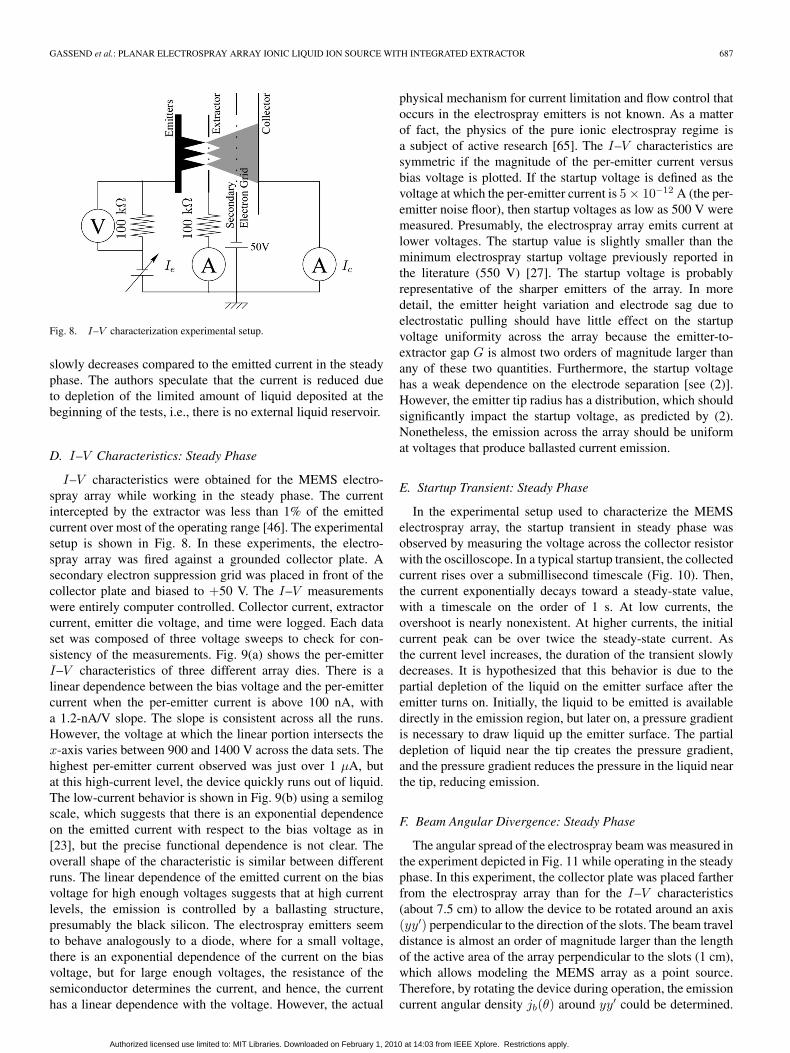
Fig. 8. I–V characterization experimental setup.
slowly decreases compared to the emitted current in the steadyphase. The authors speculate that the current is reduced dueto depletion of the limited amount of liquid deposited at thebeginning of the tests, i.e., there is no external liquid reservoir.
D. I–V Characteristics: Steady Phase
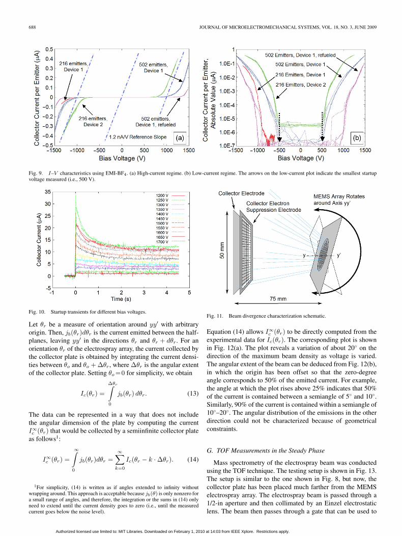
I–V characteristics were obtained for the MEMS electro-spray array while working in the steady phase. The currentintercepted by the extractor was less than 1% of the emittedcurrent over most of the operating range [46]. The experimentalsetup is shown in Fig. 8. In these experiments, the electro-spray array was fired against a grounded collector plate. Asecondary electron suppression grid was placed in front of thecollector plate and biased to +50 V. The I–V measurementswere entirely computer controlled. Collector current, extractorcurrent, emitter die voltage, and time were logged. Each dataset was composed of three voltage sweeps to check for con-sistency of the measurements. Fig. 9(a) shows the per-emitterI–V characteristics of three different array dies. There is alinear dependence between the bias voltage and the per-emittercurrent when the per-emitter current is above 100 nA, witha 1.2-nA/V slope. The slope is consistent across all the runs.However, the voltage at which the linear portion intersects thex-axis varies between 900 and 1400 V across the data sets. Thehighest per-emitter current observed was just over 1 μA, butat this high-current level, the device quickly runs out of liquid.The low-current behavior is shown in Fig. 9(b) using a semilogscale, which suggests that there is an exponential dependenceon the emitted current with respect to the bias voltage as in[23], but the precise functional dependence is not clear. Theoverall shape of the characteristic is similar between differentruns. The linear dependence of the emitted current on the biasvoltage for high enough voltages suggests that at high currentlevels, the emission is controlled by a ballasting structure,presumably the black silicon. The electrospray emitters seemto behave analogously to a diode, where for a small voltage,there is an exponential dependence of the current on the biasvoltage, but for large enough voltages, the resistance of thesemiconductor determines the current, and hence, the currenthas a linear dependence with the voltage. However, the actual
physical mechanism for current limitation and flow control thatoccurs in the electrospray emitters is not known. As a matterof fact, the physics of the pure ionic electrospray regime isa subject of active research [65]. The I–V characteristics aresymmetric if the magnitude of the per-emitter current versusbias voltage is plotted. If the startup voltage is defined as thevoltage at which the per-emitter current is 5 × 10⁻¹² A (the per-emitter noise floor), then startup voltages as low as 500 V weremeasured. Presumably, the electrospray array emits current atlower voltages. The startup value is slightly smaller than theminimum electrospray startup voltage previously reported inthe literature (550 V) [27]. The startup voltage is probablyrepresentative of the sharper emitters of the array. In moredetail, the emitter height variation and electrode sag due toelectrostatic pulling should have little effect on the startupvoltage uniformity across the array because the emitter-to-extractor gap G is almost two orders of magnitude larger thanany of these two quantities. Furthermore, the startup voltagehas a weak dependence on the electrode separation [see (2)].However, the emitter tip radius has a distribution, which shouldsignificantly impact the startup voltage, as predicted by (2).Nonetheless, the emission across the array should be uniformat voltages that produce ballasted current emission.
E. Startup Transient: Steady Phase
In the experimental setup used to characterize the MEMSelectrospray array, the startup transient in steady phase wasobserved by measuring the voltage across the collector resistorwith the oscilloscope. In a typical startup transient, the collectedcurrent rises over a submillisecond timescale (Fig. 10). Then,the current exponentially decays toward a steady-state value,with a timescale on the order of 1 s. At low currents, theovershoot is nearly nonexistent. At higher currents, the initialcurrent peak can be over twice the steady-state current. Asthe current level increases, the duration of the transient slowlydecreases. It is hypothesized that this behavior is due to thepartial depletion of the liquid on the emitter surface after theemitter turns on. Initially, the liquid to be emitted is availabledirectly in the emission region, but later on, a pressure gradientis necessary to draw liquid up the emitter surface. The partialdepletion of liquid near the tip creates the pressure gradient,and the pressure gradient reduces the pressure in the liquid nearthe tip, reducing emission.
F. Beam Angular Divergence: Steady Phase
The angular spread of the electrospray beam was measured inthe experiment depicted in Fig. 11 while operating in the steadyphase. In this experiment, the collector plate was placed fartherfrom the electrospray array than for the I–V characteristics(about 7.5 cm) to allow the device to be rotated around an axis(yy′) perpendicular to the direction of the slots. The beam traveldistance is almost an order of magnitude larger than the lengthof the active area of the array perpendicular to the slots (1 cm),which allows modeling the MEMS array as a point source.Therefore, by rotating the device during operation, the emissioncurrent angular density jb(θ) around yy′ could be determined.
Authorized licensed use limited to: MIT Libraries. Downloaded on February 1, 2010 at 14:03 from IEEE Xplore. Restrictions apply.
688 JOURNAL OF MICROELECTROMECHANICAL SYSTEMS, VOL. 18, NO. 3, JUNE 2009
Fig. 9. I–V characteristics using EMI-BF4. (a) High-current regime. (b) Low-current regime. The arrows on the low-current plot indicate the smallest startupvoltage measured (i.e., 500 V).
Fig. 10. Startup transients for different bias voltages.
Let θr be a measure of orientation around yy′ with arbitraryorigin. Then, jb(θr)dθr is the current emitted between the half-planes, leaving yy′ in the directions θr and θr + dθr. For anorientation θr of the electrospray array, the current collected bythe collector plate is obtained by integrating the current densi-ties between θo and θo + Δθr, where Δθr is the angular extentof the collector plate. Setting θo =0 for simplicity, we obtain
Ic(θr) =
Δθr∫0
jb(θr) dθr. (13)
The data can be represented in a way that does not includethe angular dimension of the plate by computing the currentI∞c (θr) that would be collected by a semiinfinite collector plateas follows1:
I∞c (θr) =
∞∫0
jb(θr)dθr =∞∑
k=0
Ic(θr − k · Δθr). (14)
1For simplicity, (14) is written as if angles extended to infinity withoutwrapping around. This approach is acceptable because jb(θ) is only nonzero fora small range of angles, and therefore, the integration or the sums in (14) onlyneed to extend until the current density goes to zero (i.e., until the measuredcurrent goes below the noise level).
Fig. 11. Beam divergence characterization schematic.
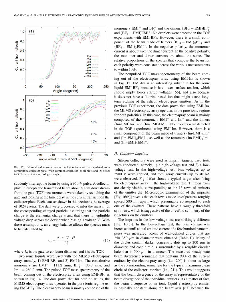
Equation (14) allows I∞c (θr) to be directly computed from theexperimental data for Ic(θr). The corresponding plot is shownin Fig. 12(a). The plot reveals a variation of about 20◦ on thedirection of the maximum beam density as voltage is varied.The angular extent of the beam can be deduced from Fig. 12(b),in which the origin has been offset so that the zero-degreeangle corresponds to 50% of the emitted current. For example,the angle at which the plot rises above 25% indicates that 50%of the current is contained between a semiangle of 5◦ and 10◦.Similarly, 90% of the current is contained within a semiangle of10◦–20◦. The angular distribution of the emissions in the otherdirection could not be characterized because of geometricalconstraints.
G. TOF Measurements in the Steady Phase
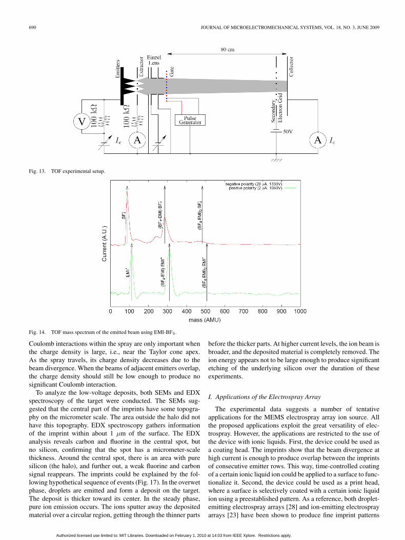
Mass spectrometry of the electrospray beam was conductedusing the TOF technique. The testing setup is shown in Fig. 13.The setup is similar to the one shown in Fig. 8, but now, thecollector plate has been placed much farther from the MEMSelectrospray array. The electrospray beam is passed through a1/2-in aperture and then collimated by an Einzel electrostaticlens. The beam then passes through a gate that can be used to
Authorized licensed use limited to: MIT Libraries. Downloaded on February 1, 2010 at 14:03 from IEEE Xplore. Restrictions apply.
GASSEND et al.: PLANAR ELECTROSPRAY ARRAY IONIC LIQUID ION SOURCE WITH INTEGRATED EXTRACTOR 689
Fig. 12. Normalized current versus device orientation, extrapolated to asemiinfinite collector plate. With common origin for (a) all plots and (b) offsetto 50% current at a zero-degree angle.
suddenly interrupt the beam by using a 950-V pulse. A collectorplate intercepts the transmitted beam about 80 cm downstreamfrom the gate. TOF measurements were taken by switching thegate and looking at the time delay in the current transient on thecollector plate. Each data set shown in this section is the averageof 1024 events. The data were processed to infer the mass m ofthe corresponding charged particle, assuming that the particlecharge is the elemental charge e and that there is negligiblevoltage drop across the device when biasing a voltage V . Withthese assumptions, an energy balance allows the species massto be calculated by
m =2 · e · V · t2
L2i
(15)
where Li is the gate-to-collector distance, and t is the TOF.Two ionic liquids were used with the MEMS electrospray
array, namely, 1) EMI-BF4 and 2) EMI-Im. The constitutivemonomers are EMI+ = 111.2 amu, BF−
4 = 86.8 amu, andIm− = 280.2 amu. The pulsed TOF mass spectrometry of thebeam coming out of the electrospray array using EMI-BF4 isshown in Fig. 14. The data prove that for both polarities, theMEMS electrospray array operates in the pure ionic regime us-ing EMI-BF4. The electrospray beam is mostly composed of the
monomers EMI+ and BF−4 and the dimers (BF4 − EMI)BF−
4
and (BF4 − EMI)EMI+. No droplets were detected in the TOFexperiments with EMI-BF4. However, there is a small com-ponent of the beam made of trimers (BF4 − EMI)2BF−
4 and(BF4 − EMI)2EMI+. In the negative polarity, the monomercurrent is about twice the dimer current. In the positive polarity,the monomer and dimer currents are about the same. Therelative proportions of the species that compose the beam foreach polarity were consistent across the various measurementsto within 10%.
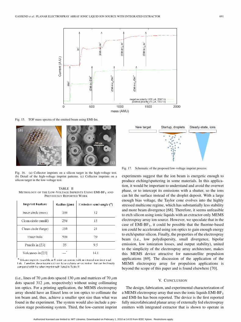
The nonpulsed TOF mass spectrometry of the beam com-ing out of the electrospray array using EMI-Im is shownin Fig. 15. EMI-Im is an interesting substitute for the ionicliquid EMI-BF4 because it has lower surface tension, whichshould imply lower startup voltages [66], and also becauseit does not have a fluorine-based ion that might cause long-term etching of the silicon electrospray emitters. As in theprevious TOF experiment, the data prove that using EMI-Im,the MEMS electrospray array operates in the pure ionic regimefor both polarities. In this case, the electrospray beam is mainlycomposed of the monomers EMI+ and Im− and the dimers(Im-EMI)Im− and (Im-EMI)EMI+. No droplets were detectedin the TOF experiments using EMI-Im. However, there is asmall component of the beam made of trimers (Im-EMI)2Im−
and (Im-EMI)2EMI+, as well as the tetramers (Im-EMI)3Im−
and (Im-EMI)3EMI+.
H. Collector Imprints
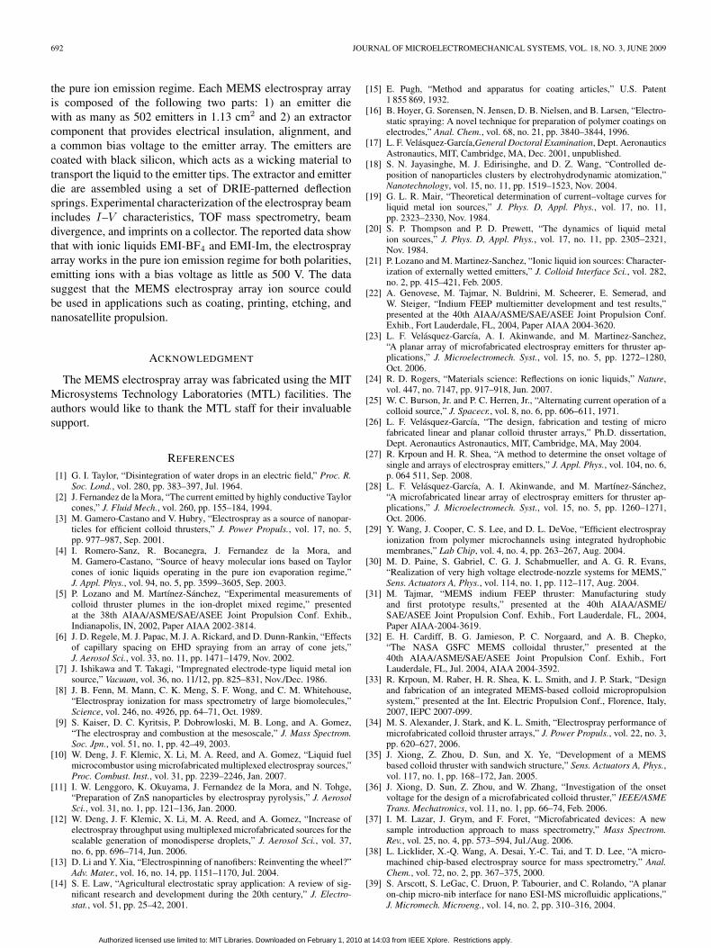
Silicon collectors were used as imprint targets. Two testswere conducted, namely, 1) a high-voltage test and 2) a low-voltage test. In the high-voltage test, bias voltages up to2500 V were applied, and total array currents up to 70 μAwere observed. Fig. 16(a) shows a typical target after firingthe electrospray array in the high-voltage test. Thirteen rowsare clearly visible, corresponding to the 13 rows of emittersof the emitter die. Microscopic examination of the imprints[Fig. 16(b)] reveals that each row is made up of patterns roughlyspaced 500 μm apart, which presumably correspond to eachone of the emitters. These patterns have a roughly threefoldsymmetry, which is suggestive of the threefold symmetry of theridgelines on the emitters.
The imprints in the low-voltage test are strikingly different[Fig. 16(c)]. In the low-voltage test, the bias voltage wasincreased until a total emitted current of a few hundred nanoam-peres was measured. Rows of well-defined circles that are250–350 μm in diameter were obtained (Table II). Many ofthe circles contain darker concentric dots up to 200 μm indiameter, and each circle is surrounded by a roughly circularhalo that is 500 μm in diameter. The measured steady-statebeam divergence semiangle that contains 90% of the currentemitted by the electrospray array (i.e., 20◦) is about as largeas the corresponding semiangle for the typical maximum cleancircle of the collector imprints (i.e., 21◦). This result suggeststhat the beam divergence of the array is representative of thebeam divergence of the individual emitters. As a matter of fact,the beam divergence of an ionic liquid electrospray emitteris basically constant along the beam axis [67] because the
Authorized licensed use limited to: MIT Libraries. Downloaded on February 1, 2010 at 14:03 from IEEE Xplore. Restrictions apply.
690 JOURNAL OF MICROELECTROMECHANICAL SYSTEMS, VOL. 18, NO. 3, JUNE 2009
Fig. 13. TOF experimental setup.
Fig. 14. TOF mass spectrum of the emitted beam using EMI-BF4.
Coulomb interactions within the spray are only important whenthe charge density is large, i.e., near the Taylor cone apex.As the spray travels, its charge density decreases due to thebeam divergence. When the beams of adjacent emitters overlap,the charge density should still be low enough to produce nosignificant Coulomb interaction.
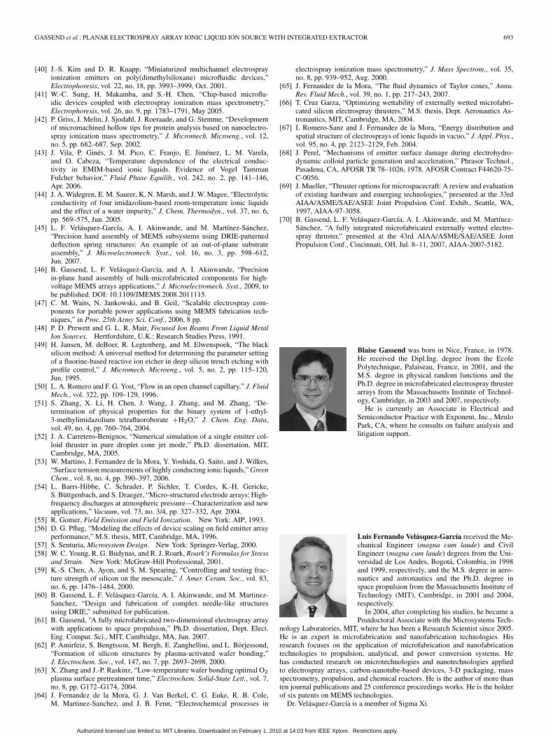
To analyze the low-voltage deposits, both SEMs and EDXspectroscopy of the target were conducted. The SEMs sug-gested that the central part of the imprints have some topogra-phy on the micrometer scale. The area outside the halo did nothave this topography. EDX spectroscopy gathers informationof the imprint within about 1 μm of the surface. The EDXanalysis reveals carbon and fluorine in the central spot, butno silicon, confirming that the spot has a micrometer-scalethickness. Around the central spot, there is an area with puresilicon (the halo), and further out, a weak fluorine and carbonsignal reappears. The imprints could be explained by the fol-lowing hypothetical sequence of events (Fig. 17). In the overwetphase, droplets are emitted and form a deposit on the target.The deposit is thicker toward its center. In the steady phase,pure ion emission occurs. The ions sputter away the depositedmaterial over a circular region, getting through the thinner parts
before the thicker parts. At higher current levels, the ion beam isbroader, and the deposited material is completely removed. Theion energy appears not to be large enough to produce significantetching of the underlying silicon over the duration of theseexperiments.
I. Applications of the Electrospray Array
The experimental data suggests a number of tentativeapplications for the MEMS electrospray array ion source. Allthe proposed applications exploit the great versatility of elec-trospray. However, the applications are restricted to the use ofthe device with ionic liquids. First, the device could be used asa coating head. The imprints show that the beam divergence athigh current is enough to produce overlap between the imprintsof consecutive emitter rows. This way, time-controlled coatingof a certain ionic liquid ion could be applied to a surface to func-tionalize it. Second, the device could be used as a print head,where a surface is selectively coated with a certain ionic liquidion using a preestablished pattern. As a reference, both droplet-emitting electrospray arrays [28] and ion-emitting electrosprayarrays [23] have been shown to produce fine imprint patterns
Authorized licensed use limited to: MIT Libraries. Downloaded on February 1, 2010 at 14:03 from IEEE Xplore. Restrictions apply.
GASSEND et al.: PLANAR ELECTROSPRAY ARRAY IONIC LIQUID ION SOURCE WITH INTEGRATED EXTRACTOR 691
Fig. 15. TOF mass spectra of the emitted beam using EMI-Im.
Fig. 16. (a) Collector imprints on a silicon target in the high-voltage test.(b) Detail of the high-voltage imprint patterns. (c) Collector imprints on asilicon target in the low-voltage test.
TABLE IIMETROLOGY OF THE LOW-VOLTAGE IMPRINTS USING EMI-BF4 AND
PREVIOUSLY REPORTED WORK
(i.e., lines of 70 μm dots spaced 130 μm and matrices of 70 μmdots spaced 312 μm, respectively) without using collimatingion optics. For a printing application, the MEMS electrosprayarray should have an Einzel lens or ion optics to collimate theion beam and, thus, achieve a smaller spot size than what wasfound in the experiment. The system would also include a pre-cision stage positioning system. Third, the low-current imprint
Fig. 17. Schematic of the proposed low-voltage imprint process.
experiments suggest that the ion beam is energetic enough toproduce etching/sputtering in some materials. In this applica-tion, it would be important to understand and avoid the overwetphase, or to intercept its emissions with a shutter, so the ionscan hit the surface instead of the droplet deposit. With a largeenough bias voltage, the Taylor cone evolves into the highlystressed multicone regime, which has substantially less stabilityand more beam divergence [68]. Therefore, it seems unfeasibleto etch silicon using ionic liquids with an extractor-only MEMSelectrospray array ion source. However, we speculate that in thecase of EMI-BF4, it could be possible that the fluorine-basedion could be accelerated using ion optics to gain enough energyto etch/sputter silicon. Finally, the properties of the electrospraybeam (i.e., low polydispersity, small divergence, bipolaremission, low ionization losses, and output stability), unitedto the simplicity of the electrospray array architecture, makesthis MEMS device attractive for nanosatellite propulsionapplications [69]. The discussion of the application of theMEMS electrospray array for propulsion applications isbeyond the scope of this paper and is found elsewhere [70].
V. CONCLUSION
The design, fabrication, and experimental characterization ofa MEMS electrospray array that uses the ionic liquids EMI-BF4
and EMI-Im has been reported. The device is the first reportedfully microfabricated planar array of externally fed electrosprayemitters with integrated extractor that is shown to operate in
Authorized licensed use limited to: MIT Libraries. Downloaded on February 1, 2010 at 14:03 from IEEE Xplore. Restrictions apply.
692 JOURNAL OF MICROELECTROMECHANICAL SYSTEMS, VOL. 18, NO. 3, JUNE 2009
the pure ion emission regime. Each MEMS electrospray arrayis composed of the following two parts: 1) an emitter diewith as many as 502 emitters in 1.13 cm2 and 2) an extractorcomponent that provides electrical insulation, alignment, anda common bias voltage to the emitter array. The emitters arecoated with black silicon, which acts as a wicking material totransport the liquid to the emitter tips. The extractor and emitterdie are assembled using a set of DRIE-patterned deflectionsprings. Experimental characterization of the electrospray beamincludes I–V characteristics, TOF mass spectrometry, beamdivergence, and imprints on a collector. The reported data showthat with ionic liquids EMI-BF4 and EMI-Im, the electrosprayarray works in the pure ion emission regime for both polarities,emitting ions with a bias voltage as little as 500 V. The datasuggest that the MEMS electrospray array ion source couldbe used in applications such as coating, printing, etching, andnanosatellite propulsion.
ACKNOWLEDGMENT
The MEMS electrospray array was fabricated using the MITMicrosystems Technology Laboratories (MTL) facilities. Theauthors would like to thank the MTL staff for their invaluablesupport.
REFERENCES
[1] G. I. Taylor, “Disintegration of water drops in an electric field,” Proc. R.Soc. Lond., vol. 280, pp. 383–397, Jul. 1964.
[2] J. Fernandez de la Mora, “The current emitted by highly conductive Taylorcones,” J. Fluid Mech., vol. 260, pp. 155–184, 1994.
[3] M. Gamero-Castano and V. Hubry, “Electrospray as a source of nanopar-ticles for efficient colloid thrusters,” J. Power Propuls., vol. 17, no. 5,pp. 977–987, Sep. 2001.
[4] I. Romero-Sanz, R. Bocanegra, J. Fernandez de la Mora, andM. Gamero-Castano, “Source of heavy molecular ions based on Taylorcones of ionic liquids operating in the pure ion evaporation regime,”J. Appl. Phys., vol. 94, no. 5, pp. 3599–3605, Sep. 2003.
[5] P. Lozano and M. Martínez-Sánchez, “Experimental measurements ofcolloid thruster plumes in the ion-droplet mixed regime,” presentedat the 38th AIAA/ASME/SAE/ASEE Joint Propulsion Conf. Exhib.,Indianapolis, IN, 2002, Paper AIAA 2002-3814.
[6] J. D. Regele, M. J. Papac, M. J. A. Rickard, and D. Dunn-Rankin, “Effectsof capillary spacing on EHD spraying from an array of cone jets,”J. Aerosol Sci., vol. 33, no. 11, pp. 1471–1479, Nov. 2002.
[7] J. Ishikawa and T. Takagi, “Impregnated electrode-type liquid metal ionsource,” Vacuum, vol. 36, no. 11/12, pp. 825–831, Nov./Dec. 1986.
[8] J. B. Fenn, M. Mann, C. K. Meng, S. F. Wong, and C. M. Whitehouse,“Electrospray ionization for mass spectrometry of large biomolecules,”Science, vol. 246, no. 4926, pp. 64–71, Oct. 1989.
[9] S. Kaiser, D. C. Kyritsis, P. Dobrowloski, M. B. Long, and A. Gomez,“The electrospray and combustion at the mesoscale,” J. Mass Spectrom.Soc. Jpn., vol. 51, no. 1, pp. 42–49, 2003.
[10] W. Deng, J. F. Klemic, X. Li, M. A. Reed, and A. Gomez, “Liquid fuelmicrocombustor using microfabricated multiplexed electrospray sources,”Proc. Combust. Inst., vol. 31, pp. 2239–2246, Jan. 2007.
[11] I. W. Lenggoro, K. Okuyama, J. Fernandez de la Mora, and N. Tohge,“Preparation of ZnS nanoparticles by electrospray pyrolysis,” J. AerosolSci., vol. 31, no. 1, pp. 121–136, Jan. 2000.
[12] W. Deng, J. F. Klemic, X. Li, M. A. Reed, and A. Gomez, “Increase ofelectrospray throughput using multiplexed microfabricated sources for thescalable generation of monodisperse droplets,” J. Aerosol Sci., vol. 37,no. 6, pp. 696–714, Jun. 2006.
[13] D. Li and Y. Xia, “Electrospinning of nanofibers: Reinventing the wheel?”Adv. Mater., vol. 16, no. 14, pp. 1151–1170, Jul. 2004.
[14] S. E. Law, “Agricultural electrostatic spray application: A review of sig-nificant research and development during the 20th century,” J. Electro-stat., vol. 51, pp. 25–42, 2001.
[15] E. Pugh, “Method and apparatus for coating articles,” U.S. Patent1 855 869, 1932.
[16] B. Hoyer, G. Sorensen, N. Jensen, D. B. Nielsen, and B. Larsen, “Electro-static spraying: A novel technique for preparation of polymer coatings onelectrodes,” Anal. Chem., vol. 68, no. 21, pp. 3840–3844, 1996.
[17] L. F. Velásquez-García,General Doctoral Examination, Dept. AeronauticsAstronautics, MIT, Cambridge, MA, Dec. 2001, unpublished.
[18] S. N. Jayasinghe, M. J. Edirisinghe, and D. Z. Wang, “Controlled de-position of nanoparticles clusters by electrohydrodynamic atomization,”Nanotechnology, vol. 15, no. 11, pp. 1519–1523, Nov. 2004.
[19] G. L. R. Mair, “Theoretical determination of current–voltage curves forliquid metal ion sources,” J. Phys. D, Appl. Phys., vol. 17, no. 11,pp. 2323–2330, Nov. 1984.
[20] S. P. Thompson and P. D. Prewett, “The dynamics of liquid metalion sources,” J. Phys. D, Appl. Phys., vol. 17, no. 11, pp. 2305–2321,Nov. 1984.
[21] P. Lozano and M. Martinez-Sanchez, “Ionic liquid ion sources: Character-ization of externally wetted emitters,” J. Colloid Interface Sci., vol. 282,no. 2, pp. 415–421, Feb. 2005.
[22] A. Genovese, M. Tajmar, N. Buldrini, M. Scheerer, E. Semerad, andW. Steiger, “Indium FEEP multiemitter development and test results,”presented at the 40th AIAA/ASME/SAE/ASEE Joint Propulsion Conf.Exhib., Fort Lauderdale, FL, 2004, Paper AIAA 2004-3620.
[23] L. F. Velásquez-García, A. I. Akinwande, and M. Martinez-Sanchez,“A planar array of microfabricated electrospray emitters for thruster ap-plications,” J. Microelectromech. Syst., vol. 15, no. 5, pp. 1272–1280,Oct. 2006.
[24] R. D. Rogers, “Materials science: Reflections on ionic liquids,” Nature,vol. 447, no. 7147, pp. 917–918, Jun. 2007.
[25] W. C. Burson, Jr. and P. C. Herren, Jr., “Alternating current operation of acolloid source,” J. Spacecr., vol. 8, no. 6, pp. 606–611, 1971.
[26] L. F. Velásquez-García, “The design, fabrication and testing of microfabricated linear and planar colloid thruster arrays,” Ph.D. dissertation,Dept. Aeronautics Astronautics, MIT, Cambridge, MA, May 2004.
[27] R. Krpoun and H. R. Shea, “A method to determine the onset voltage ofsingle and arrays of electrospray emitters,” J. Appl. Phys., vol. 104, no. 6,p. 064 511, Sep. 2008.
[28] L. F. Velásquez-García, A. I. Akinwande, and M. Martínez-Sánchez,“A microfabricated linear array of electrospray emitters for thruster ap-plications,” J. Microelectromech. Syst., vol. 15, no. 5, pp. 1260–1271,Oct. 2006.
[29] Y. Wang, J. Cooper, C. S. Lee, and D. L. DeVoe, “Efficient electrosprayionization from polymer microchannels using integrated hydrophobicmembranes,” Lab Chip, vol. 4, no. 4, pp. 263–267, Aug. 2004.
[30] M. D. Paine, S. Gabriel, C. G. J. Schabmueller, and A. G. R. Evans,“Realization of very high voltage electrode-nozzle systems for MEMS,”Sens. Actuators A, Phys., vol. 114, no. 1, pp. 112–117, Aug. 2004.
[31] M. Tajmar, “MEMS indium FEEP thruster: Manufacturing studyand first prototype results,” presented at the 40th AIAA/ASME/SAE/ASEE Joint Propulsion Conf. Exhib., Fort Lauderdale, FL, 2004,Paper AIAA-2004-3619.
[32] E. H. Cardiff, B. G. Jamieson, P. C. Norgaard, and A. B. Chepko,“The NASA GSFC MEMS colloidal thruster,” presented at the40th AIAA/ASME/SAE/ASEE Joint Propulsion Conf. Exhib., FortLauderdale, FL, Jul. 2004, AIAA 2004-3592.
[33] R. Krpoun, M. Raber, H. R. Shea, K. L. Smith, and J. P. Stark, “Designand fabrication of an integrated MEMS-based colloid micropropulsionsystem,” presented at the Int. Electric Propulsion Conf., Florence, Italy,2007, IEPC 2007-099.
[34] M. S. Alexander, J. Stark, and K. L. Smith, “Electrospray performance ofmicrofabricated colloid thruster arrays,” J. Power Propuls., vol. 22, no. 3,pp. 620–627, 2006.
[35] J. Xiong, Z. Zhou, D. Sun, and X. Ye, “Development of a MEMSbased colloid thruster with sandwich structure,” Sens. Actuators A, Phys.,vol. 117, no. 1, pp. 168–172, Jan. 2005.
[36] J. Xiong, D. Sun, Z. Zhou, and W. Zhang, “Investigation of the onsetvoltage for the design of a microfabricated colloid thruster,” IEEE/ASMETrans. Mechatronics, vol. 11, no. 1, pp. 66–74, Feb. 2006.
[37] I. M. Lazar, J. Grym, and F. Foret, “Microfabricated devices: A newsample introduction approach to mass spectrometry,” Mass Spectrom.Rev., vol. 25, no. 4, pp. 573–594, Jul./Aug. 2006.
[38] L. Licklider, X.-Q. Wang, A. Desai, Y.-C. Tai, and T. D. Lee, “A micro-machined chip-based electrospray source for mass spectrometry,” Anal.Chem., vol. 72, no. 2, pp. 367–375, 2000.
[39] S. Arscott, S. LeGac, C. Druon, P. Tabourier, and C. Rolando, “A planaron-chip micro-nib interface for nano ESI-MS microfluidic applications,”J. Micromech. Microeng., vol. 14, no. 2, pp. 310–316, 2004.
Authorized licensed use limited to: MIT Libraries. Downloaded on February 1, 2010 at 14:03 from IEEE Xplore. Restrictions apply.
GASSEND et al.: PLANAR ELECTROSPRAY ARRAY IONIC LIQUID ION SOURCE WITH INTEGRATED EXTRACTOR 693
[40] J.-S. Kim and D. R. Knapp, “Miniaturized multichannel electrosprayionization emitters on poly(dimethylsiloxane) microfluidic devices,”Electrophoresis, vol. 22, no. 18, pp. 3993–3999, Oct. 2001.
[41] W.-C. Sung, H. Makamba, and S.-H. Chen, “Chip-based microflu-idic devices coupled with electrospray ionization mass spectrometry,”Electrophoresis, vol. 26, no. 9, pp. 1783–1791, May 2005.
[42] P. Griss, J. Melin, J. Sjodahl, J. Roeraade, and G. Stemme, “Developmentof micromachined hollow tips for protein analysis based on nanoelectro-spray ionization mass spectrometry,” J. Micromech. Microeng., vol. 12,no. 5, pp. 682–687, Sep. 2002.
[43] J. Vila, P. Ginés, J. M. Pico, C. Franjo, E. Jiménez, L. M. Varela,and O. Cabeza, “Temperature dependence of the electrical conduc-tivity in EMIM-based ionic liquids. Evidence of Vogel TammanFulcher behavior,” Fluid Phase Equilib., vol. 242, no. 2, pp. 141–146,Apr. 2006.
[44] J. A. Widegren, E. M. Saurer, K. N. Marsh, and J. W. Magee, “Electrolyticconductivity of four imidazolium-based room-temperature ionic liquidsand the effect of a water impurity,” J. Chem. Thermodyn., vol. 37, no. 6,pp. 569–575, Jun. 2005.
[45] L. F. Velásquez-García, A. I. Akinwande, and M. Martínez-Sánchez,“Precision hand assembly of MEMS subsystems using DRIE-patterneddeflection spring structures: An example of an out-of-plane substrateassembly,” J. Microelectromech. Syst., vol. 16, no. 3, pp. 598–612,Jun. 2007.
[46] B. Gassend, L. F. Velásquez-García, and A. I. Akinwande, “Precisionin-plane hand assembly of bulk-microfabricated components for high-voltage MEMS arrays applications,” J. Microelectromech. Syst., 2009, tobe published. DOI: 10.1109/JMEMS.2008.2011115.
[47] C. M. Waits, N. Jankowski, and B. Geil, “Scalable electrospray com-ponents for portable power applications using MEMS fabrication tech-niques,” in Proc. 25th Army Sci. Conf., 2006, 8 pp.
[48] P. D. Prewett and G. L. R. Mair, Focused Ion Beams From Liquid MetalIon Sources. Hertfordshire, U.K.: Research Studies Press, 1991.
[49] H. Jansen, M. deBoer, R. Legtenberg, and M. Elwenspoek, “The blacksilicon method: A universal method for determining the parameter settingof a fluorine-based reactive ion etcher in deep silicon trench etching withprofile control,” J. Micromech. Microeng., vol. 5, no. 2, pp. 115–120,Jun. 1995.
[50] L. A. Romero and F. G. Yost, “Flow in an open channel capillary,” J. FluidMech., vol. 322, pp. 109–129, 1996.
[51] S. Zhang, X. Li, H. Chen, J. Wang, J. Zhang, and M. Zhang, “De-termination of physical properties for the binary system of 1-ethyl-3-methylimidazolium tetrafluoroborate +H2O,” J. Chem. Eng. Data,vol. 49, no. 4, pp. 760–764, 2004.
[52] J. A. Carretero-Benignos, “Numerical simulation of a single emitter col-loid thruster in pure droplet cone jet mode,” Ph.D. dissertation, MIT,Cambridge, MA, 2005.
[53] W. Martino, J. Fernandez de la Mora, Y. Yoshida, G. Saito, and J. Wilkes,“Surface tension measurements of highly conducting ionic liquids,” GreenChem., vol. 8, no. 4, pp. 390–397, 2006.
[54] L. Barrs-Hibbe, C. Schrader, P. Sichler, T. Cordes, K.-H. Gericke,S. Büttgenbach, and S. Draeger, “Micro-structured electrode arrays: High-frequency discharges at atmospheric pressure—Characterization and newapplications,” Vacuum, vol. 73, no. 3/4, pp. 327–332, Apr. 2004.
[55] R. Gomer, Field Emission and Field Ionization. New York: AIP, 1993.[56] D. G. Pflug, “Modeling the effects of device scaling on field emitter array
performance,” M.S. thesis, MIT, Cambridge, MA, 1996.[57] S. Senturia, Microsystem Design. New York: Springer-Verlag, 2000.[58] W. C. Young, R. G. Budynas, and R. J. Roark, Roark’s Formulas for Stress
and Strain. New York: McGraw-Hill Professional, 2001.[59] K.-S. Chen, A. Ayon, and S. M. Spearing, “Controlling and testing frac-
ture strength of silicon on the mesoscale,” J. Amer. Ceram. Soc., vol. 83,no. 6, pp. 1476–1484, 2000.
[60] B. Gassend, L. F. Velásquez-García, A. I. Akinwande, and M. Martinez-Sanchez, “Design and fabrication of complex needle-like structuresusing DRIE,” submitted for publication.
[61] B. Gassend, “A fully microfabricated two-dimensional electrospray arraywith applications to space propulsion,” Ph.D. dissertation, Dept. Elect.Eng. Comput. Sci., MIT, Cambridge, MA, Jun. 2007.
[62] P. Amirfeiz, S. Bengtsson, M. Bergh, E. Zanghellini, and L. Börjessond,“Formation of silicon structures by plasma-activated wafer bonding,”J. Electrochem. Soc., vol. 147, no. 7, pp. 2693–2698, 2000.
[63] X. Zhang and J.-P. Raskinz, “Low-temperature wafer bonding optimal O2
plasma surface pretreatment time,” Electrochem. Solid-State Lett., vol. 7,no. 8, pp. G172–G174, 2004.
[64] J. Fernandez de la Mora, G. J. Van Berkel, C. G. Euke, R. B. Cole,M. Martinez-Sanchez, and J. B. Fenn, “Electrochemical processes in
electrospray ionization mass spectrometry,” J. Mass Spectrom., vol. 35,no. 8, pp. 939–952, Aug. 2000.
[65] J. Fernandez de la Mora, “The fluid dynamics of Taylor cones,” Annu.Rev. Fluid Mech., vol. 39, no. 1, pp. 217–243, 2007.
[66] T. Cruz Garza, “Optimizing wettability of externally wetted microfabri-cated silicon electrospray thrusters,” M.S. thesis, Dept. Aeronautics As-tronautics, MIT, Cambridge, MA, 2004.
[67] I. Romero-Sanz and J. Fernandez de la Mora, “Energy distribution andspatial structure of electrosprays of ionic liquids in vacuo,” J. Appl. Phys.,vol. 95, no. 4, pp. 2123–2129, Feb. 2004.
[68] J. Perel, “Mechanisms of emitter surface damage during electrohydro-dynamic colloid particle generation and acceleration,” Phrasor Technol.,Pasadena, CA, AFOSR TR 78–1026, 1978. AFOSR Contract F44620-75-C-0056.
[69] J. Mueller, “Thruster options for microspacecraft: A review and evaluationof existing hardware and emerging technologies,” presented at the 33rdAIAA/ASME/SAE/ASEE Joint Propulsion Conf. Exhib., Seattle, WA,1997, AIAA-97-3058.
[70] B. Gassend, L. F. Velásquez-García, A. I. Akinwande, and M. Martínez-Sánchez, “A fully integrated microfabricated externally wetted electro-spray thruster,” presented at the 43rd AIAA/ASME/SAE/ASEE JointPropulsion Conf., Cincinnati, OH, Jul. 8–11, 2007, AIAA-2007-5182.
Blaise Gassend was born in Nice, France, in 1978.He received the Dipl.Ing. degree from the EcolePolytechnique, Palaiseau, France, in 2001, and theM.S. degree in physical random functions and thePh.D. degree in microfabricated electrospray thrusterarrays from the Massachusetts Institute of Technol-ogy, Cambridge, in 2003 and 2007, respectively.
He is currently an Associate in Electrical andSemiconductor Practice with Exponent, Inc., MenloPark, CA, where he consults on failure analysis andlitigation support.
Luis Fernando Velásquez-García received the Me-chanical Engineer (magna cum laude) and CivilEngineer (magna cum laude) degrees from the Uni-versidad de Los Andes, Bogotá, Colombia, in 1998and 1999, respectively, and the M.S. degree in aero-nautics and astronautics and the Ph.D. degree inspace propulsion from the Massachusetts Institute ofTechnology (MIT), Cambridge, in 2001 and 2004,respectively.
In 2004, after completing his studies, he became aPostdoctoral Associate with the Microsystems Tech-
nology Laboratories, MIT, where he has been a Research Scientist since 2005.He is an expert in microfabrication and nanofabrication technologies. Hisresearch focuses on the application of microfabrication and nanofabricationtechnologies to propulsion, analytical, and power conversion systems. Hehas conducted research on microtechnologies and nanotechnologies appliedto electrospray arrays, carbon-nanotube-based devices, 3-D packaging, massspectrometry, propulsion, and chemical reactors. He is the author of more thanten journal publications and 25 conference proceedings works. He is the holderof six patents on MEMS technologies.
Dr. Velásquez-García is a member of Sigma Xi.
Authorized licensed use limited to: MIT Libraries. Downloaded on February 1, 2010 at 14:03 from IEEE Xplore. Restrictions apply.
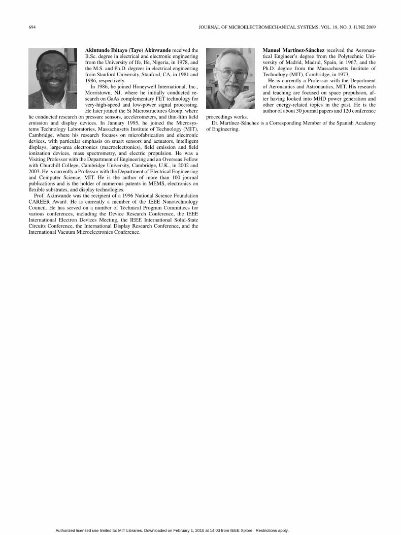
694 JOURNAL OF MICROELECTROMECHANICAL SYSTEMS, VOL. 18, NO. 3, JUNE 2009
Akintunde Ibitayo (Tayo) Akinwande received theB.Sc. degree in electrical and electronic engineeringfrom the University of Ife, Ife, Nigeria, in 1978, andthe M.S. and Ph.D. degrees in electrical engineeringfrom Stanford University, Stanford, CA, in 1981 and1986, respectively.
In 1986, he joined Honeywell International, Inc.,Morristown, NJ, where he initially conducted re-search on GaAs complementary FET technology forvery-high-speed and low-power signal processing.He later joined the Si Microstructures Group, where
he conducted research on pressure sensors, accelerometers, and thin-film fieldemission and display devices. In January 1995, he joined the Microsys-tems Technology Laboratories, Massachusetts Institute of Technology (MIT),Cambridge, where his research focuses on microfabrication and electronicdevices, with particular emphasis on smart sensors and actuators, intelligentdisplays, large-area electronics (macroelectronics), field emission and fieldionization devices, mass spectrometry, and electric propulsion. He was aVisiting Professor with the Department of Engineering and an Overseas Fellowwith Churchill College, Cambridge University, Cambridge, U.K., in 2002 and2003. He is currently a Professor with the Department of Electrical Engineeringand Computer Science, MIT. He is the author of more than 100 journalpublications and is the holder of numerous patents in MEMS, electronics onflexible substrates, and display technologies.
Prof. Akinwande was the recipient of a 1996 National Science FoundationCAREER Award. He is currently a member of the IEEE NanotechnologyCouncil. He has served on a number of Technical Program Committees forvarious conferences, including the Device Research Conference, the IEEEInternational Electron Devices Meeting, the IEEE International Solid-StateCircuits Conference, the International Display Research Conference, and theInternational Vacuum Microelectronics Conference.
Manuel Martínez-Sánchez received the Aeronau-tical Engineer’s degree from the Polytechnic Uni-versity of Madrid, Madrid, Spain, in 1967, and thePh.D. degree from the Massachusetts Institute ofTechnology (MIT), Cambridge, in 1973.
He is currently a Professor with the Departmentof Aeronautics and Astronautics, MIT. His researchand teaching are focused on space propulsion, af-ter having looked into MHD power generation andother energy-related topics in the past. He is theauthor of about 30 journal papers and 120 conference
proceedings works.Dr. Martínez-Sánchez is a Corresponding Member of the Spanish Academy
of Engineering.
Authorized licensed use limited to: MIT Libraries. Downloaded on February 1, 2010 at 14:03 from IEEE Xplore. Restrictions apply.


![Advanced Drug Delivery Reviews · 2021. 4. 12. · field of controlled drug delivery systems [28,29]. Microfabricated drug devices incorporate planar geometries with low aspect ratio,](https://img.pdfslide.net/doc/110x75/6145c45f07bb162e665fe61e/advanced-drug-delivery-reviews-2021-4-12-ield-of-controlled-drug-delivery.jpg)