Embed Size (px)
Citation preview
A Multimedia DSP processor design
Master Thesis by
Vladimir Gnatyuk & Christian Runesson
LiTH-ISY-EX-3530-2004
Supervisor: Dake Liu
Examiner: Dake Liu
Linköping, 2004

Avdelning, InstitutionDivision, Department
Institutionen för systemteknik581 83 LINKÖPING
DatumDate2004- 03- 29
SpråkLanguage
RapporttypReport category
ISBN
Svenska/SwedishX Engelska /English
LicentiatavhandlingX Examensarbete
ISRN LITH- ISY- EX- 3530- 2004
C- uppsatsD- uppsats
Serietitel och serienummerTitle of series, numbering
ISSN
Övrig rapport____
URL för elektronisk versionhttp: / / w w w.ep.liu.se /exjobb/isy /2004 /3530/
TitelTitle
Design av en Multimedia DSP Processor
A Multimedia DSP Processor Design
Författare Author
Vladimir Gnatyuk & Christian Runesson
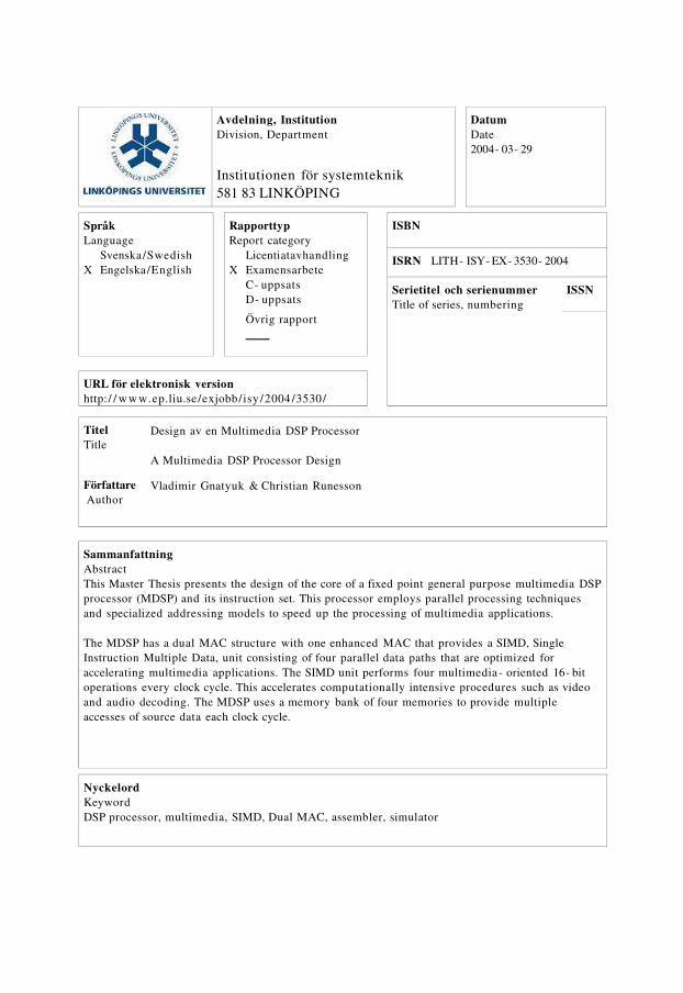
SammanfattningAbstractThis Master Thesis presents the design of the core of a fixed point general purpose multimedia DSPprocessor (MDSP) and its instruction set. This processor employs parallel processing techniquesand specialized addressing models to speed up the processing of multimedia applications.
The MDSP has a dual MAC structure with one enhanced MAC that provides a SIMD, SingleInstruction Multiple Data, unit consisting of four parallel data paths that are optimized foraccelerating multimedia applications. The SIMD unit performs four multimedia- oriented 16- bitoperations every clock cycle. This accelerates computationally intensive procedures such as videoand audio decoding. The MDSP uses a memory bank of four memories to provide multipleaccesses of source data each clock cycle.
NyckelordKeywordDSP processor, multimedia, SIMD, Dual MAC, assembler, simulator

Abstract
This Master Thesis presents the design of the core of a fixed point generalpurpose multimedia DSP processor (MDSP) and its instruction set. Thisprocessor employs parallel processing techniques and specializedaddressing models to speed up the processing of multimedia applications.
The MDSP has a dual MAC structure with one enhanced MAC that provides aSIMD, Single Instruction Multiple Data, unit consisting of four parallel datapaths that are optimized for accelerating multimedia applications. The SIMDunit performs four multimedia-oriented 16-bit operations every clock cycle.This accelerates computationally intensive procedures such as video andaudio decoding. The MDSP uses a memory bank of four memories to providemultiple accesses of source data each clock cycle.

Acknowledgments
This work have been done for the Division of Computer Engineering,Department of Electrical Engineering at Linköping University, Sweden. We want to thank all the people who were involved in our work during allthis weeks for their help, assistance and the instance to the authors.
We want to give our special thanks to:
1. Professor Dake Liu, our supervisor, for such an interesting topic, forscience advices and for opportunity to study the essence of the DSPprocessor design.
2. Ph.D student Eric Tell, for assisting and helpful advices during the work.
3. Ph.D student Daniel Wiklund, for solving some computer relatedproblems.

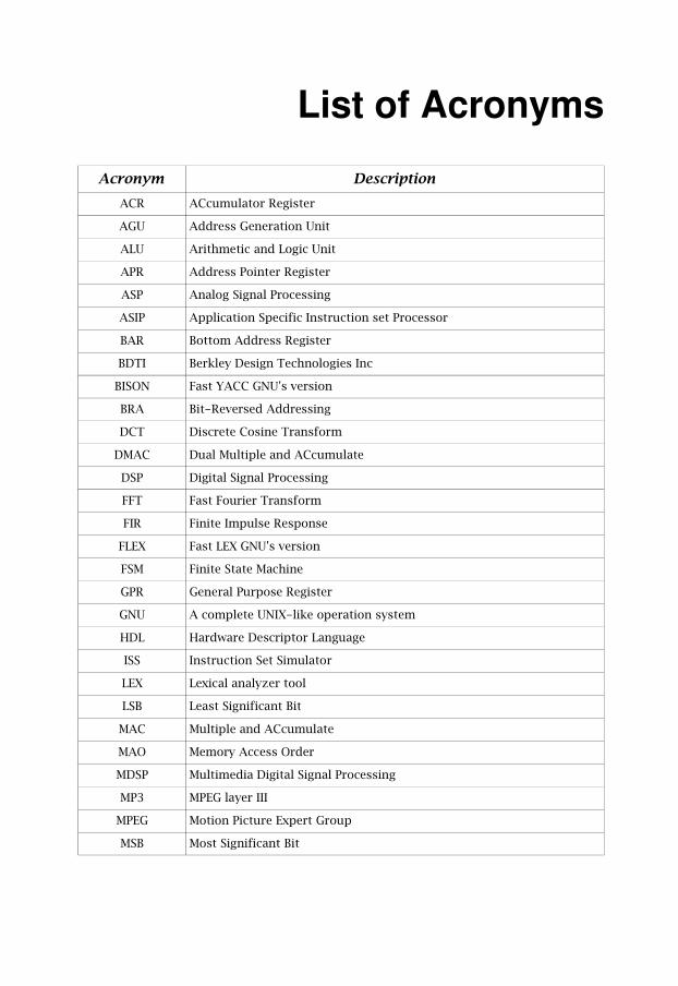
List of Acronyms
Acronym DescriptionACR ACcumulator Register
AGU Address Generation Unit
ALU Arithmetic and Logic Unit
APR Address Pointer Register
ASP Analog Signal Processing
ASIP Application Specific Instruction set Processor
BAR Bottom Address Register
BDTI Berkley Design Technologies Inc
BISON Fast YACC GNU's version
BRA Bit-Reversed Addressing
DCT Discrete Cosine Transform
DMAC Dual Multiple and ACcumulate
DSP Digital Signal Processing
FFT Fast Fourier Transform
FIR Finite Impulse Response
FLEX Fast LEX GNU's version
FSM Finite State Machine
GPR General Purpose Register
GNU A complete UNIX-like operation system
HDL Hardware Descriptor Language
ISS Instruction Set Simulator
LEX Lexical analyzer tool
LSB Least Significant Bit
MAC Multiple and ACcumulate
MAO Memory Access Order
MDSP Multimedia Digital Signal Processing
MP3 MPEG layer III
MPEG Motion Picture Expert Group
MSB Most Significant Bit
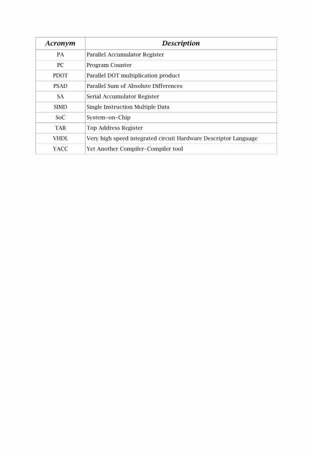
Acronym DescriptionPA Parallel Accumulator Register
PC Program Counter
PDOT Parallel DOT multiplication product
PSAD Parallel Sum of Absolute Differences
SA Serial Accumulator Register
SIMD Single Instruction Multiple Data
SoC System-on-Chip
TAR Top Address Register
VHDL Very high speed integrated circuit Hardware Descriptor Language
YACC Yet Another Compiler-Compiler tool
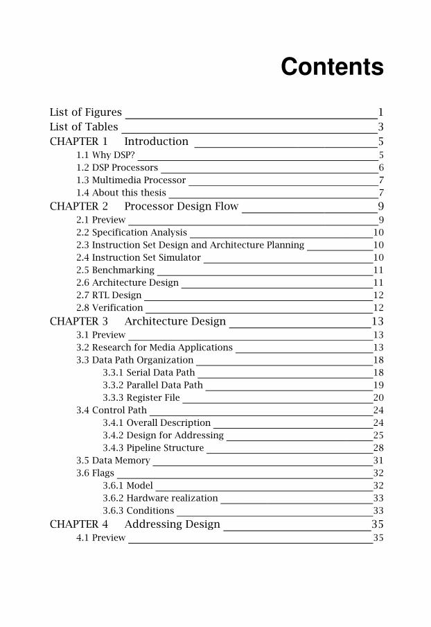
Contents
List of Figures 1List of Tables 3CHAPTER 1 Introduction 5
1.1 Why DSP? 51.2 DSP Processors 61.3 Multimedia Processor 71.4 About this thesis 7
CHAPTER 2 Processor Design Flow 92.1 Preview 92.2 Specification Analysis 102.3 Instruction Set Design and Architecture Planning 102.4 Instruction Set Simulator 102.5 Benchmarking 112.6 Architecture Design 112.7 RTL Design 122.8 Verification 12
CHAPTER 3 Architecture Design 133.1 Preview 133.2 Research for Media Applications 133.3 Data Path Organization 18
3.3.1 Serial Data Path 183.3.2 Parallel Data Path 193.3.3 Register File 20
3.4 Control Path 243.4.1 Overall Description 243.4.2 Design for Addressing 253.4.3 Pipeline Structure 28
3.5 Data Memory 313.6 Flags 32
3.6.1 Model 323.6.2 Hardware realization 333.6.3 Conditions 33
CHAPTER 4 Addressing Design 354.1 Preview 35
4.2 Hardware Model 354.3 Addressing Model 364.4 Addressing Modes 38
CHAPTER 5 Instruction Set Design 435.1 Preview 435.2 Hardware Description 44
5.2.1 The STATUS register 445.2.2 Partitioning between configurable and programmable 455.2.3 Additional specifiers in the status register 45
5.3 MOVE 475.3.1 MOVE model 475.3.2 MOVE instruction word 475.3.3 MOVE addressing model 50
5.4 ALU 525.4.1 ALU model 525.4.2 ALU instruction word 535.4.3 ALU addressing model 56
5.5 MAC 585.5.1 MAC model 585.5.2 MAC instruction word 595.5.3 MAC addressing model 61
5.6 DMAC 635.6.1 DMAC model 635.6.2 DMAC instruction word 645.6.3 DMAC addressing model 67
5.7 SIMD 705.7.1 SIMD model 705.7.2 SIMD instruction word 715.7.3 SIMD addressing model 75
5.8 PROGRAM FLOW 785.8.1 Program Flow model 785.8.2 Program Flow instruction word 79
CHAPTER 6 Assembler Design 816.1 Preview 816.2 Tools Description 816.3 Assembler Design Flow 846.4 Assembler Features 856.5 Results 86
CHAPTER 7 Instruction Set Simulator Design 877.1 Preview 877.2 Simulator Model 877.3 The Start Procedure 887.4 The Load Procedure 897.5 The Execute Procedure 907.6 Results 93
CHAPTER 8 Benchmarking 958.1 Preview 958.2 Benchmarking Strategy 958.3 Results 96
CHAPTER 9 Conclusions 979.1 Results 979.2 Future work and improvements 98
Appendix A.1 Serial Data Path 99Appendix A.2 Parallel Data Path 101Appendix B.1 A guide to the instruction set 103Appendix B.2 Instructions Description 123Bibliography 207


List of Figures
Figure Description PageFigure 2.1 The DSP processor design flow 9
Figure 3.1 A top-level Data Path architecture 14
Figure 3.2 The six data paths MDSP structure 16
Figure 3.3 General and special purposes registers space 21
Figure 3.4 Register File structure 22
Figure 3.5 Control Path structure 24
Figure 3.6 Address Generation Logic structure 27
Figure 3.7 Pipeline structure 28
Figure 3.8 Variable 5- and 6-step pipeline stages 29
Figure 3.9 Pipeline data hazard 30
Figure 3.10 Data memory structure 31
Figure 3.11 The p_flags register 32
Figure 3.12 The s_flags register 32
Figure 5.1 The status register, STATUS 45
Figure 5.2 MOVE instruction word 48
Figure 5.3 The MOVE addressing flow graph 50
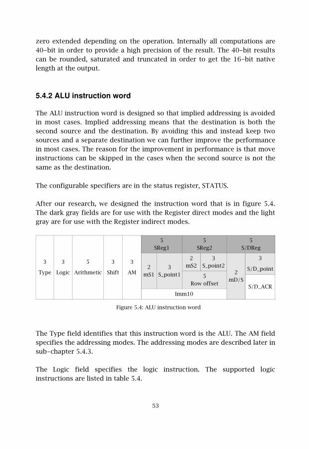
Figure 5.4 ALU instruction word 53
Figure 5.5 The ALU addressing flow graph 56
Figure 5.6 MAC instruction word 59
Figure 5.7 The MAC addressing flow graph 61
Figure 5.8 DMAC instruction word 65
Figure 5.9 The DMAC addressing flow graph 68
Figure 5.10 SIMD instruction word 72
Figure 5.11 The SIMD addressing flow graph 76
Figure 5.12 P_FLOW instruction word 79
Figure 6.1 Compiler design flow diagram 83
Figure 6.2 Assembler Design Flow 84
Figure 7.1 The start procedure 88
Figure 7.2 The load procedure 89
�

Figure Description PageFigure 7.3 The execute procedure 92
�
List of Tables
Table Description PageTable 3.1 Condition table 33
Table 4.1 Addressing with an individual offset of two 37
Table 4.2 Addressing modes 38
Table 4.3 Example of BRA with masking 40
Table 4.4 Selection of the table register 40
Table 4.5 Description of the TABLE field 41
Table 5.1 MOVE instruction list 48
Table 5.2 MOVE addressing modes 51
Table 5.3 Extended addressing modes 51
Table 5.4 LOGIC instruction list 54
Table 5.5 ARITHMETIC instruction list 54
Table 5.6 SHIFT instruction list 55
Table 5.7 ALU addressing modes 57
Table 5.8 MAC instruction list 60
Table 5.9 MAC addressing modes 62
Table 5.10 DMAC instruction list 66
Table 5.11 DMAC addressing modes 69
Table 5.12 Data path enabling via MAO when using the 8-bit mode 73
Table 5.13 Data path enabling via MAO when using the 16-bit mode 73
Table 5.14 SIMD instruction list 75
Table 5.15 SIMD addressing modes 77
Table 5.16 P_FLOW instruction list 80
Table 5.17 Description of the conditional instructions 80
Table 8.1 FIR benchmark 96
�

�
1Introduction
1.1 Why DSP?
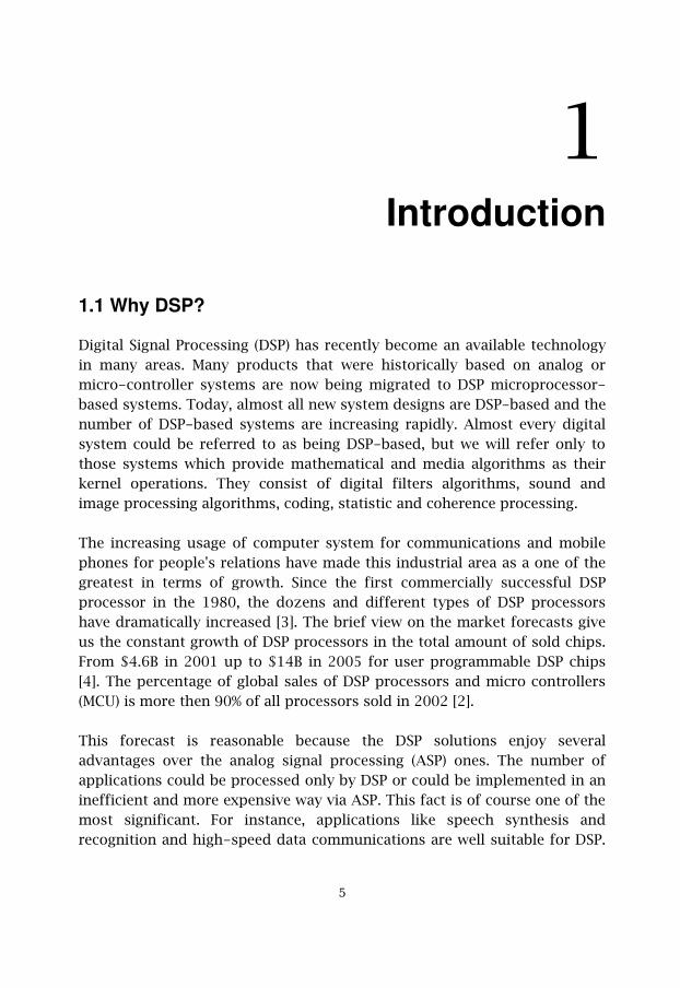
Digital Signal Processing (DSP) has recently become an available technologyin many areas. Many products that were historically based on analog ormicro-controller systems are now being migrated to DSP microprocessor-based systems. Today, almost all new system designs are DSP-based and thenumber of DSP-based systems are increasing rapidly. Almost every digitalsystem could be referred to as being DSP-based, but we will refer only tothose systems which provide mathematical and media algorithms as theirkernel operations. They consist of digital filters algorithms, sound andimage processing algorithms, coding, statistic and coherence processing.
The increasing usage of computer system for communications and mobilephones for people's relations have made this industrial area as a one of thegreatest in terms of growth. Since the first commercially successful DSPprocessor in the 1980, the dozens and different types of DSP processorshave dramatically increased [3]. The brief view on the market forecasts giveus the constant growth of DSP processors in the total amount of sold chips.From $4.6B in 2001 up to $14B in 2005 for user programmable DSP chips[4]. The percentage of global sales of DSP processors and micro controllers(MCU) is more then 90% of all processors sold in 2002 [2].
This forecast is reasonable because the DSP solutions enjoy severaladvantages over the analog signal processing (ASP) ones. The number ofapplications could be processed only by DSP or could be implemented in aninefficient and more expensive way via ASP. This fact is of course one of themost significant. For instance, applications like speech synthesis andrecognition and high-speed data communications are well suitable for DSP.
�
The predictable behavior, re-programmability and the sizes of the systemsare also very important and they do all benefit from using DSP.
1.2 DSP processors
A DSP processor is a processor that performs one or several DSP algorithms.They were designed to perform mathematical algorithms in real timedomain. This is a main reason for the DSP processors development.
A DSP processor is, because of the nature of DSP algorithms, a processormainly oriented on multiply-accumulate operations. The number ofoperations in DSP are similar to each other and this gives the opportunity toprovide efficient parallelization of the calculations. Next beneficial featureof a DSP processor is the multiple-access memory architecture to improveprocessing. There are several ways to organize the support for simultaneousaccesses to multiple memory locations. It can be done with the use of multi-ported memories, multiple buses and multiple independent memories in amemory bank. Next significant and often used feature for speeding up thedata processing is to use one or more dedicated address generation unitsand, usually, with special addressing models. This feature gives multipleaddress calculations at the same instruction cycle. Some special addressmodels are designed exclusively for speeding up certain DSP algorithms.
There are two big categories of DSP processors that are dominating, thegeneral purpose DSP processors and the Application Specific Instruction setProcessor (ASIP). They also could be specified by the used algorithms,sample rate, clock rate and arithmetic types. A general purpose DSPprocessor gives enough flexibility, design environment support, andapplication references. For some reasons like critical requirements on thesilicon area, power consumption, performance and especially when aSystem-on-Chip (Soc) solution is required, we need to use an ASIP DSPprocessor instead of general purpose DSP processor [2].
�
1.3 Multimedia processor
A Multimedia Processor is an application specific DSP processor whichperforms a number of multimedia algorithms. The following classes of DSPalgorithms might be referred to as multimedia types:� Speech coding and decoding� Speech recognition� Speech identification� High-fidelity audio encoding and decoding� Modem algorithms� Audio mixing and editing� Voice synthesis� Image compression and decompression� Image compositing
A general purpose Multimedia DSP (MDSP) processor should, of course,cover all of the above. Naturally, no processor can meet the needs of all oreven the most of the applications, and that is why it's a designer's task tofind the optimal trade-off between functional covering and performance,cost, integration, power consumption, and other factors.
1.4 About this thesis
The purpose of this project was to design a programmable Multimedia DSPprocessor, according to the given specification, for the Division of ComputerEngineering, Department of Electrical Engineering at Linköping University,Sweden. This work started at the processor research step, with analysis of agiven specification, and stopped at the benchmarking design step because ofthe lack of time in this 20 weeks of length job. The architecture, theinstruction set and the coding solutions have been designed as flexible aspossible for future improvements and corrections.
This introductory chapter explains what a DSP is, why the vendors are usingit and also gives the main definitions and observations. Chapter 2 describeshow the DSP processor should be designed. It introduces the processordesign flow chart and gives a brief description for each step. Chapter 3presents the detailed description of the Architecture Design step, allresearch issues and the designers features for optimal specification
�

implementation are specified here. The address generation strategy andexisting addressing models are described in Chapter 4. The designedInstruction Set is presented in Chapter 5. Chapter 6 describes the assemblerdesign and Chapter 7 shows the simulator design. The Benchmarking designstep is described in Chapter 8. Finally we will analyze the results and willgive our conclusions in Chapter 9.
Appendix A.1 shows the Serial Data Path architecture. Appendix A.2 shows four Parallel Data Paths architecture.Appendix B.1 contains the guide to the instruction set.Appendix B.2 has a complete description of all instructions for thisprocessor.
�
2Processor Design Flow
2.1 Preview
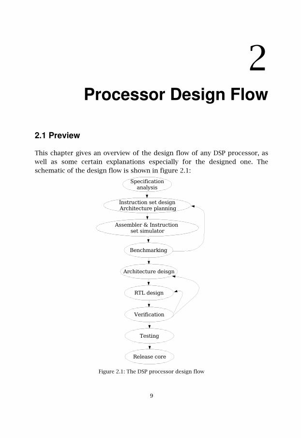
This chapter gives an overview of the design flow of any DSP processor, aswell as some certain explanations especially for the designed one. Theschematic of the design flow is shown in figure 2.1:
Figure 2.1: The DSP processor design flow
�� ��� �������������
������ ������������������ ���� �������������
����� ����!������� ������������������
"�� ����#���
�� ���� �����������
$%&�������
'����� �����
%������
$������� ���

2.2 Specification Analysis
The design analysis have started from reading and understanding of thegiven specification. The following issues have been researched:� Flexibility of supported operations� Number of computing resources� Memory capacity� Flexible and multiple memory accesses� Parallelism of the architecture� Low power design� Opportunities for future accelerations
2.3 Instruction Set Design and Architecture Planning
During this design step the designers should decide what data types andwhat instructions that should be used in the processor. It mainly dependson what tasks and operations the future processor is designed for. At thisdesign step the instruction types and formats should also be defined andfixed. All these activities should be provided within the processorarchitecture planning at a top level.
Instruction format strongly depends on the architecture topology, numberof processing units, memory banks, interconnections and relations betweenthem. In addition, the designers should always match the possibility ofimplementing each instruction according to the available hardware. Afterthis step the, top-level processor architecture and the detailed instructionset are defined. These activities are described in chapters 3, 4 and 5.
2.4 Instruction Set Simulator
The instruction set simulator is a behavioral model of the processor that iswritten in some high-level language [1]. It needs to check the designedinstruction set from the functional point of view. Each instruction should beimplemented and verified. In conjunction with the benchmarking step, thesimulator should give the answer if the designed instruction set andtemporal architecture covers the processor's performance requirements ornot.
�(
The behavioral model of the processor consists of two parts, the assemblerprogram and the instruction set simulator. The assembler firstly translatesthe lexical code (assembly program) to a suitable form for the existedhardware as hexadecimal code. In reality this hexadecimal code shouldgenerate the control signals to provide all necessary computations in thedata path. The instruction set simulator is virtually responsible for this.
A detailed description of the assembler design is given in chapters 6 and theinstruction set simulator design is given in chapter 7.
2.5 Benchmarking
Now, when the instruction set simulator is ready, it is time to write the realcode for the future processor and pass it through the processor. Usually themost popular or most significant applications for this processor are used tocompare the results with vendors or maybe with some other related works.
This step verifies the designed instruction set, if it offers sufficientperformance to fulfill the requirements, that were set up duringspecification analysis and architecture planning. If it does we could talkabout the release of the instruction set. If it does not, we have to go back tothe instruction set design level and modify it. Please refer to chapter 8 fordetails.
2.6 Architecture Design
This step is a real hardware implementation, using the top-down approach.All computational units, buses, control blocks, other elementary andauxiliary units are defined at the register-transfer level. All blocks,processing elements and data chains must follow the hardware limitationsand instruction set requirements.
��
2.7 RTL Design
A modern implementation method is to use one of the hardware descriptorlanguages (HDL). The most usable languages are VHDL and Verilog. Theselanguages let the programmer write synthesizeable code. It might be veryuseful for testing prototypes.
2.8 Verification
Verification is a very important and a very time consuming design step. Itcan consume up to 80% of the complete design time for some systems. Thisstep is the designers final one before manufacturing. The verification isdivided into the functional and the physical verification. The first oneverifies the logical correctness of the HDL code, the second one handles thephysical parameters, for example time constrains [2]. If there were no errorsduring the verification process, the RTL implementation version of theprocessor is released. Otherwise we have to modify the RTL code or forsome reasons even change the architecture. See the design flow diagram infigure 2.1.
Because of the time deficit and the specific type of this 20 weeks length job,the architecture of the processor unfortunately have not been fixed andimplemented yet.
��
3Architecture Design
3.1 Preview
A DSP processor can be divided into its processor core and its peripherals.In this job we have concentrated on the processor core design. The coremight be divided later into the data path, the control path, the memory, thebuses, and the flags.
This chapter describes the architecture issues, the design decisions andtheir reasonings. It also gives the overall design conception and a detailedresearch process.
3.2 Research for Media Applications
According to the design specification we have designed a multimedia DSPprocessor (MDSP). This is a DSP processor that has special architecture andhardware features to accelerate the media applications. The data have afixed-point representation. The general structure of the processor is aHarvard's one, with different memories for programs and for data.
There are several architectural DSP features. Most of the DSP applicationsrequire high performance in repetitive computation and data intensivetasks. The research is aimed for designing of an efficient architecture, forthe general purpose multimedia processor, and is concentrated on:
1) Fast Multiply-Accumulate (MAC) operations (the most DSP algorithms, including filtering and transforms, are multiplication-intensive).
2) Multiple memory access architecture (this property might be very efficient in cases where the operations could be accelerated by reading
��
multiple data items at the same instruction cycle).3) Specialized address models (efficient data managing and special data
types in the DSP applications).
The designers should not forget about an efficient Control Path and of theinput/output organization. In this work we did not concentrate on them.
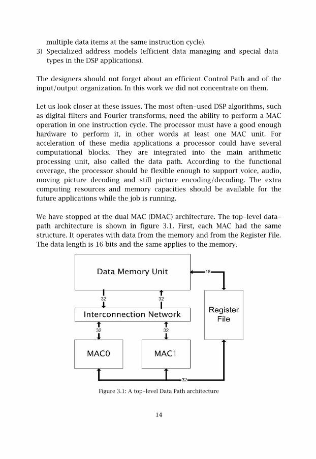
Let us look closer at these issues. The most often-used DSP algorithms, suchas digital filters and Fourier transforms, need the ability to perform a MACoperation in one instruction cycle. The processor must have a good enoughhardware to perform it, in other words at least one MAC unit. Foracceleration of these media applications a processor could have severalcomputational blocks. They are integrated into the main arithmeticprocessing unit, also called the data path. According to the functionalcoverage, the processor should be flexible enough to support voice, audio,moving picture decoding and still picture encoding/decoding. The extracomputing resources and memory capacities should be available for thefuture applications while the job is running.
We have stopped at the dual MAC (DMAC) architecture. The top-level data-path architecture is shown in figure 3.1. First, each MAC had the samestructure. It operates with data from the memory and from the Register File.The data length is 16 bits and the same applies to the memory.
Figure 3.1: A top-level Data Path architecture
��
Because the media data have an 8-bit data length representation, the furtherresearch was aimed at the 8-bit operations acceleration. The most commonmedia tasks as motion estimation and motion compensation require 8-bitadditions and multiplications. This was the main reason for our architectureimprovement, the extended MAC0 structure. The extra computationalhardware has been added to employ parallel processing techniques such assingle instruction multiple data (SIMD).
Four additional MAC units have been integrated into MAC0 for parallelcomputations. At this moment, six computational paths exist. Four paralleldata paths, specialized for media applications, and two serial data paths, seefigure 3.2:
��
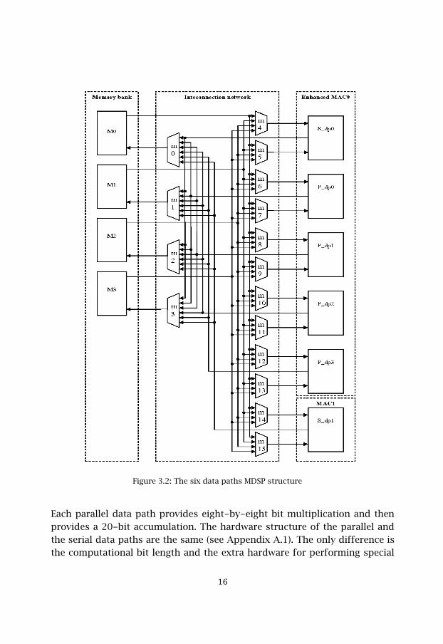
Each parallel data path provides eight-by-eight bit multiplication and thenprovides a 20-bit accumulation. The hardware structure of the parallel andthe serial data paths are the same (see Appendix A.1). The only difference isthe computational bit length and the extra hardware for performing special
��
Figure 3.2: The six data paths MDSP structure
instructions like PSAD and PDOT. Chapter 5 gives a detailed description ofthese instructions. Each parallel data path has a final 20-bit result and eachserial data path has a 40-bit result. These bit lengths have been got byadding the guard bits to a native length result to prevent overflow errorsduring the hardware loops. For the large loops, and according to generalpurpose preference of this MDSP processor, we found that four guard bitsfor the final result in the parallel data paths, and eight guard bits for theserial ones are enough.
In order to speed up media applications, we divided the memory bank intofour memories. This gives us the ability to read up to four different data atthe same instruction cycle and of course to write them back. A theoreticalspeed up of up to four times can be achieved for long loop tasks. Thememory access strategy is as follows:
� All data paths can read data from any memory� The serial data path can write data to any memory in the memory bank
while the parallel data paths only can write to its own memory. Forinstance P_dp0 writes to memory0 (M0)
All wires are of 16-bit width, the native processor length. In case of parallelcomputations, when the SIMD mode is enabled, data can be represented intwo ways:
1) As two 8-bit operands in one 16-bit address space to provide eight by eight operations.
2) As one 16-bit operand in each memory address space.
In conclusion, this processor may:� Process 8-bit media data in SIMD mode� Process 16-bit data in single and Dual MAC modes� Provide mixed usage of both of the above modes (DMAC) for as much
processing acceleration as possible� Provide any memory access order in SIMD and DMAC modes using the
special address calculation techniques, that are described in chapter 4.
��
3.3 Data Path Organization
The data path of the designed MDSP consists of two serial data paths andfour parallel data paths. The Register file and the memory structure are alsodescribed in this sub-chapter.
3.3.1 Serial Data Path
Appendix A.1 shows the detailed serial data path architecture. The serialdata path was designed according to the current instruction set in order toprovide all the arithmetic, logic, and shift instructions. The serial data pathrepresents a MAC structure so it's also possible to provide sixteen-by-sixteen multiplications and then provide one or several arithmetic, logic orshift operations. According to the instruction word, data can also bebypassed through the multiplication chain and reach the arithmetic, logicand shift part of the data path.
The serial data path was designed according to the co-designed instructionset. The instruction set consists of six types of instructions: � MOVE instructions� ALU instructions� MAC instructions� DMAC instructions� SIMD instructions� P_FLOW instructions
Please refer to chapter 5 for a detailed description of the instruction set.
From the computational point of view, only ALU, MAC and DMAC types ofinstructions can be used in the serial data path.
The architecture supports the ability to provide three ALU operations perone instruction word as one arithmetic, one logic and one shift instruction.In other words it can provide:� arithmetic + logic + shift operations� arithmetic operation only� logic operation only� shift operation only
��
� any combination of arithmetic, logic and shift operations one time each,and exactly in this strong order of execution. This processor can executeonly the arithmetic then the logic and then the shift operation. Thislimitation of the executional order is not so ineffective because up to 80%of all the cases, this exact order is the one that is needed. We applied thistrade-off in our design. This statistic percent number we have got fromthe previous research activities.
All possible arithmetic, logic and shift operations are listed and described inchapter 5.
The MAC and DMAC instructions are also passing through the serial datapath, but in this case the multiplication access chain is always enabled bythe corresponding control signals.
3.3.2 Parallel Data Path
The organization of the parallel data path (see Appendix A.2) is absolutelythe same as for the serial data path except for some architecture features: � Parallel data paths can operate with 8-bit data, providing eight-by-eight
multiplications, and then accumulate the 20-bit result � Parallel data paths operates only with the SIMD instructions� Parallel data paths processes the data only from the memory bank� The operands in the parallel data paths are taken from the same memory
address line or, if the individual offset is defined, from the differentaddresses which have been shifted according to this offset. A moredetailed description of the individual offset addressing is in chapter 4. Inother words, data should be prepared in the memory like two 8-bit piecesof data at the same address line. One piece in the 8-bit most significantpart and the other one in the 8-bit least significant part of the 16-bitmemory word. The usual 16-bit operand usage is also possible here forany other non-multiplication operations. See the detailed SIMDinstructions description in chapter 5
� Extra hardware have been added for the possibility to provide PDOT andPSAD instructions
�
3.3.3 Register File
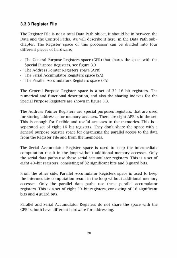
The Register File is not a total Data Path object, it should be in between theData and the Control Paths. We will describe it here, in the Data Path sub-chapter. The Register space of this processor can be divided into fourdifferent pieces of hardware:
� The General Purpose Registers space (GPR) that shares the space with theSpecial Purpose Registers, see figure 3.3
� The Address Pointer Registers space (APR)� The Serial Accumulator Registers space (SA)� The Parallel Accumulators Registers space (PA)
The General Purpose Register space is a set of 32 16-bit registers. Thenumerical and functional description, and also the sharing indexes for theSpecial Purpose Registers are shown in figure 3.3.
The Address Pointer Registers are special purposes registers, that are usedfor storing addresses for memory accesses. There are eight APR`s in the set.This is enough for flexible and useful accesses to the memories. This is aseparated set of eight 16-bit registers. They don't share the space with ageneral purpose register space for organizing the parallel access to the datafrom the Register File and from the memories.
The Serial Accumulator Register space is used to keep the intermediatecomputation result in the loop without additional memory accesses. Onlythe serial data paths use these serial accumulator registers. This is a set ofeight 40-bit registers, consisting of 32 significant bits and 8 guard bits.
From the other side, Parallel Accumulator Registers space is used to keepthe intermediate computation result in the loop without additional memoryaccesses. Only the parallel data paths use these parallel accumulatorregisters. This is a set of eight 20-bit registers, consisting of 16 significantbits and 4 guard bits.
Parallel and Serial Accumulator Registers do not share the space with theGPR`s, both have different hardware for addressing.
�(
15 0R0
R1
R2
R3
R4
R5
R6
R7
R8
R9
R10
R11
R12
R13
R14
R15
R16
R17
R18
R19
R20
R21/TR0
R22/TR1
R23/TR2
R24/TR3
R25/TAR0
R26/BAR0
R27/TAR1
R28/BAR1
R29/COL_OFFSET
R30/IND_OFFSET
R31/STATUS
Figure 3.3: General and special purposes registers space
��
��
Figure 3.4: Register File Structure

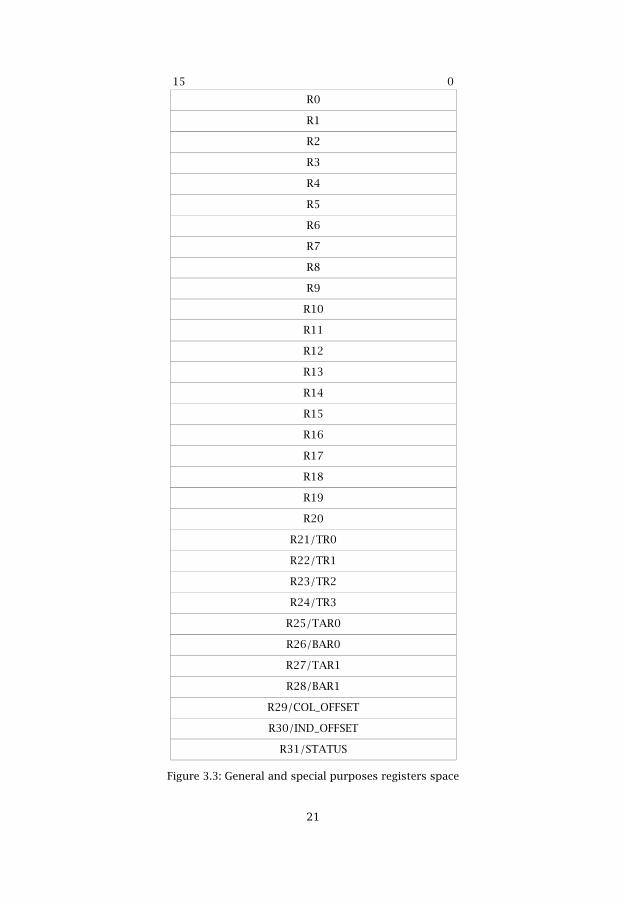
The Special Purpose Register space is a set of registers for auxiliarypurposes, for special computation cases, for processor control status andfor configuration. A more detailed description is in Appendix B.1.
The Register File provides up to four different read accesses and twodifferent write accesses the same instruction cycle. Both MAC0 and MAC1can write data to any register. The special control logic is responsible forchoosing the correct chain in the input multiplexers, see figure 3.4.
��
3.4 Control Path
This sub-chapter gives the overall description of the control path for thisprocessor. In this work we did not concentrate on the detailed design of thecontrol path but have proposed the core's solutions and root designingfeatures. The main task of the Control Path is to provide the program flowcontrol. It supplies the correct instruction to execute, decodes instructionsinto control signals and it manages asynchronous job [2]. It also shouldsupply the correct order of instruction execution by the program counter(PC).
3.4.1 Overall Description
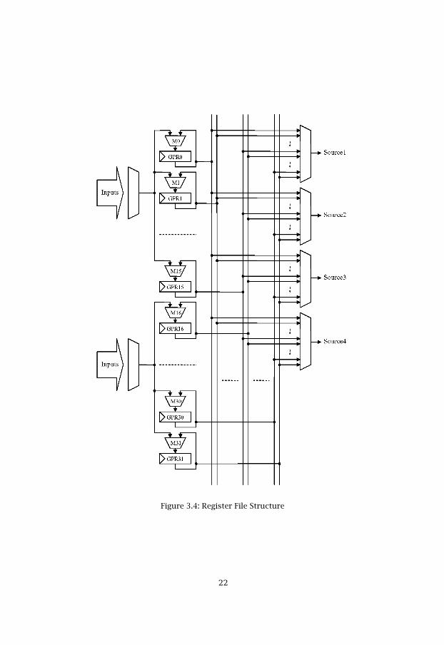
The simplified version of the Control Path is shown in figure 3.5 andcontains the programmable Finite State Machine (FSM) or the Program FlowController, Program memory, and Instruction decoder.
The Program Flow Controller reads the flag registers and status signals fromthe processor. It manages the next PC address for program memoryaddressing according to the execution of the current instruction. The nextinstruction, pushes the current instruction from the program memory to theinstruction decoder. The program memory is a 32-bit wide, 64kW largememory.
Figure 3.5: Control Path structure
��

The Instruction decoder processes an instruction word and generates thecontrol signals to the Data Path, to the data memory, and of course to allrequired parts of the processor. The Instruction decoder also providesaddress generation for the data according to the instruction word. Later wewill discuss the addressing design strategy and the pipeline instructionexecution for the designed processor.
3.4.2 Design for Addressing
During the processor design we can distinguish between two types ofaddressing strategies. The operand addressing and the program addressing.The program addressing is executed in the Program Flow Controller. Theoperand addressing means memory addressing and register addressing.
Program addressing calculates the valid sequence number of every nextinstruction. In other words it calculates the valid PC address. The sequenceof events is, first the control logic should fetch an instruction from theprogram memory according to the current PC address, then it shoulddecode the fetched instruction and generate the necessary control signals.After defining if the next instruction is a branch or not, the calculation logicshould generate the valid PC address for the next fetching. The designedprocessor could generate the following addresses:
� PC <= PC + 1 – not a jump instruction� PC <= PC + 1 – a jump instruction, but jump is not taken� PC <= jump address – a jump instruction, jump is taken
A more detailed description of the branching techniques in the programflow control logic is in the William Stallings reference text book [7].
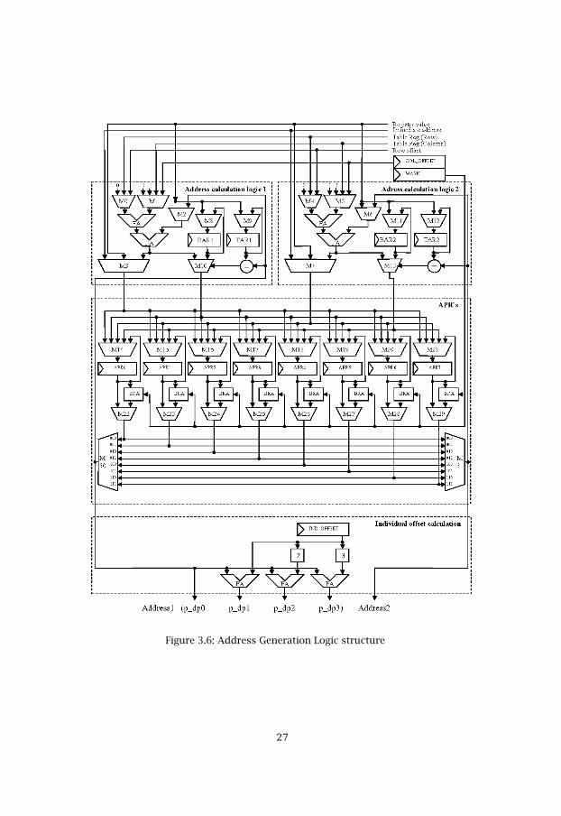
The operand addressing is one of the toughest processor design step,because it consumes much more coding then the other parts. According tothe architecture plan we need to calculate two different addresses at thesame instruction cycle. For this reason two identical address generationlogics have been designed, see figure 3.6.
The main addressing research result is a special addressing mode, thetotally flexible Memory Index addressing mode. It uses a special offset
��

technique by composing the so-called row and column offsets. The detaileddescription of the addressing strategy that has been used in this processorcan be found in chapter 4.
��
��
Figure 3.6: Address Generation Logic structure
3.4.3 Pipeline Structure
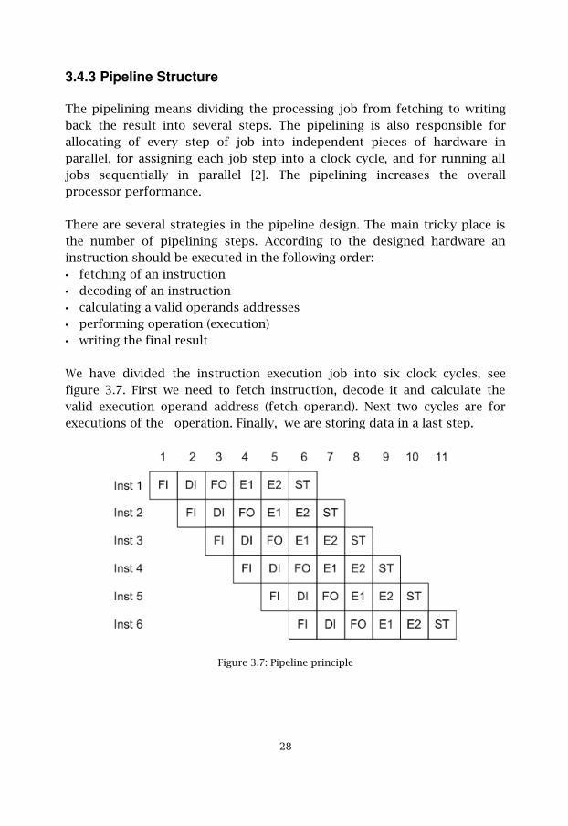
The pipelining means dividing the processing job from fetching to writingback the result into several steps. The pipelining is also responsible forallocating of every step of job into independent pieces of hardware inparallel, for assigning each job step into a clock cycle, and for running alljobs sequentially in parallel [2]. The pipelining increases the overallprocessor performance.
There are several strategies in the pipeline design. The main tricky place isthe number of pipelining steps. According to the designed hardware aninstruction should be executed in the following order: � fetching of an instruction� decoding of an instruction� calculating a valid operands addresses� performing operation (execution)� writing the final result
We have divided the instruction execution job into six clock cycles, seefigure 3.7. First we need to fetch instruction, decode it and calculate thevalid execution operand address (fetch operand). Next two cycles are forexecutions of the operation. Finally, we are storing data in a last step.
Figure 3.7: Pipeline principle
��
where: FI – fetch instructionDI – decode instructionFO – fetch operandE1 – performing the 1-st operationE2 – performing the 2-nd operationST – store the result
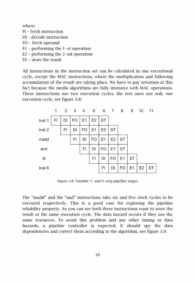
All instructions in the instruction set can be calculated in one executionalcycle, except the MAC instructions, where the multiplication and followingaccumulation of the result are taking place. We have to pay attention at thisfact because the media algorithms are fully intensive with MAC operations.These instructions use two execution cycles, the rest ones use only oneexecution cycle, see figure 3.8:
Figure 3.8: Variable 5- and 6-step pipeline stages
The “madd” and the “and” instructions take six and five clock cycles to beexecuted respectively. This is a good case for exploring the pipelinereliability property. As you can see both these instructions want to store theresult at the same execution cycle. The data hazard occurs if they use thesame resources. To avoid this problem and any other timing or datahazards, a pipeline controller is expected. It should spy the datadependencies and correct them according to the algorithm, see figure 3.9:
�
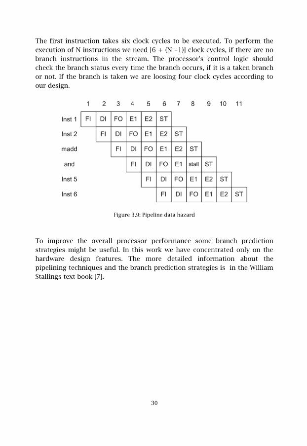
The first instruction takes six clock cycles to be executed. To perform theexecution of N instructions we need [6 + (N -1)] clock cycles, if there are nobranch instructions in the stream. The processor's control logic shouldcheck the branch status every time the branch occurs, if it is a taken branchor not. If the branch is taken we are loosing four clock cycles according toour design.
Figure 3.9: Pipeline data hazard
To improve the overall processor performance some branch predictionstrategies might be useful. In this work we have concentrated only on thehardware design features. The more detailed information about thepipelining techniques and the branch prediction strategies is in the WilliamStallings text book [7].
�(
3.5 Data Memory
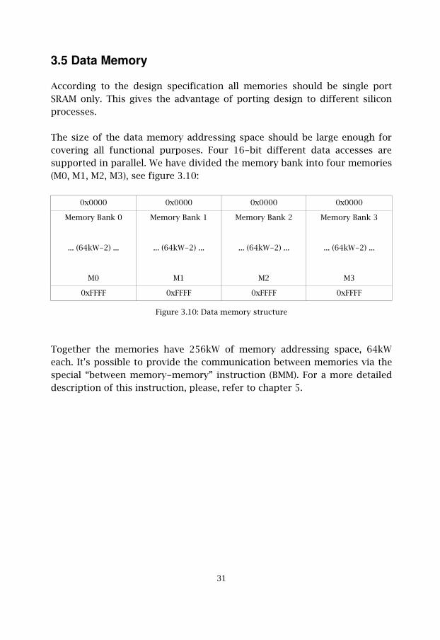
According to the design specification all memories should be single portSRAM only. This gives the advantage of porting design to different siliconprocesses.
The size of the data memory addressing space should be large enough forcovering all functional purposes. Four 16-bit different data accesses aresupported in parallel. We have divided the memory bank into four memories(M0, M1, M2, M3), see figure 3.10:
0x0000 0x0000 0x0000 0x0000
Memory Bank 0
... (64kW-2) ...
M0
Memory Bank 1
... (64kW-2) ...
M1
Memory Bank 2
... (64kW-2) ...
M2
Memory Bank 3
... (64kW-2) ...
M3
0xFFFF 0xFFFF 0xFFFF 0xFFFF
Figure 3.10: Data memory structure
Together the memories have 256kW of memory addressing space, 64kWeach. It's possible to provide the communication between memories via thespecial “between memory-memory” instruction (BMM). For a more detaileddescription of this instruction, please, refer to chapter 5.
��
3.6 Flags
This DSP processor uses a set of four flags that are updated after most ofthe operations. The flags describe the internal computation status of theprocessor. They are checked before using the conditional executioninstructions.
The flags are N, Z, C and O. The N flag is set when the result is negative, theZ flag is set when the result is zero, the C flag is set when there is a carryout and the O flag is set when there is a overflow. The flags are reset as soonas the conditions are not fulfilled any more.
3.6.1 Model
Each data path has it's own set of flags. This is only a preparation for thefuture and in this design they all work as one set of flags. As an example, allO flags must be set in order to have overflow as the computational status.The flags in the parallel data path0 are called p_N0, p_Z0, p_C0 and p_O0. Inparallel data path1 they are called p_N1, p_Z1, p_C1 and p_O1 and so on. Inthe serial data paths the flags are called s_N0, s_Z0, s_C0, s_O0 and s_N1,s_Z1, s_C1, s_O1. The index always specifies the data path number and the por s specifies if it's a parallel or a serial data path.
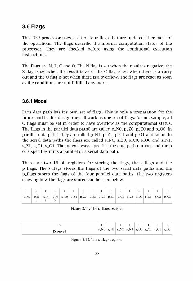
There are two 16-bit registers for storing the flags, the s_flags and thep_flags. The s_flags stores the flags of the two serial data paths and thep_flags stores the flags of the four parallel data paths. The two registersshowing how the flags are stored can be seen below.
1
p_N0
1
p_N1
1
p_N2
1
p_N3
1
p_Z0
1
p_Z1
1
p_Z2
1
p_Z3
1
p_C0
1
p_C1
1
p_C2
1
p_C3
1
p_O0
1
p_O1
1
p_O2
1
p_O3
Figure 3.11: The p_flags register
8
Reserved
1s_N0
1s_N1
1s_N2
1s_N3
1s_O0
1s_O1
1s_O2
1s_O3
Figure 3.12: The s_flags register
��
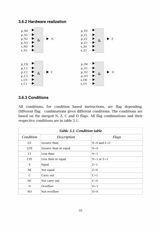
3.6.2 Hardware realization p_N0 p_Z0 p_N1 p_Z1 p_N2 N p_Z2 Z p_N3 p_Z3 s_N0 s_Z0 s_N1 s_Z1 p_C0 p_O0 p_C1 p_O1 p_C2 C p_O2 O p_C3 p_O3 s_C0 s_O0 s_C1 s_O1
3.6.3 Conditions
All conditions, for condition based instructions, are flag depending.Different flag combinations gives different conditions. The conditions arebased on the merged N, Z, C and O flags. All flag combinations and theirrespective conditions are in table 3.1.
Table 3.1: Condition table
Condition Description FlagsGT Greater than N=0 and Z=0
GTE Greater than or equal N=0
LT Less than N=1
LTE Less than or equal N=1 or Z=1
E Equal Z=1
NE Not equal Z=0
C Carry out C=1
NC Not carry out C=0
O Overflow O=1
NO Not overflow O=0
��
! !
! !

��
4Addressing design
4.1 Preview
The task of the address generation unit, AGU, is to generate the correct 16-bit addresses each clock cycle. The AGU is designed so it can access up tofour memories at the same clock cycle. The memories can be accessed withan individual offset between each of them. The data can be addressed withcolumn and row offsets for a very flexible addressing. The AGU alsosupports Modulo addressing and BRA, bit reversed addressing, as well asmost other basic addressing. Exactly what is supported and not is describedin this chapter.
4.2 Hardware Model
Two different addresses can be calculated at the same time from twoidentical address calculation logics inside the AGU, see figure 3.6. There is atop address register, the TAR, and a bottom address register, the BAR, thatsupports modulo addressing for each address calculation logic. There is alsosupport for bit reversed addressing, BRA. The BRA supports masking ofMSB`s. How many MSB`s that should be masked is checked in the MASKregister. There are two special offset registers, the IND_OFFSET thatspecifies the offset between memories and the COL_OFFSET that specifieshow large the column offset should be. The Row offset is taken from theinstruction word`s. There are four Table registers that specifies the lengthof the row and column offset when using Memory index addressing.
��
4.3 Addressing Model
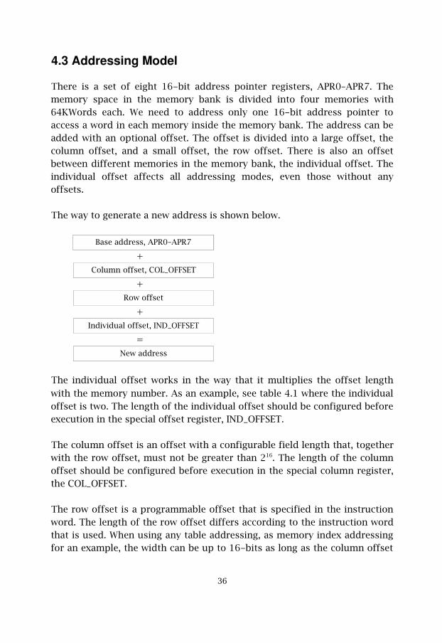
There is a set of eight 16-bit address pointer registers, APR0–APR7. Thememory space in the memory bank is divided into four memories with64KWords each. We need to address only one 16-bit address pointer toaccess a word in each memory inside the memory bank. The address can beadded with an optional offset. The offset is divided into a large offset, thecolumn offset, and a small offset, the row offset. There is also an offsetbetween different memories in the memory bank, the individual offset. Theindividual offset affects all addressing modes, even those without anyoffsets.
The way to generate a new address is shown below.
Base address, APR0–APR7
+Column offset, COL_OFFSET
+Row offset
+Individual offset, IND_OFFSET
=New address
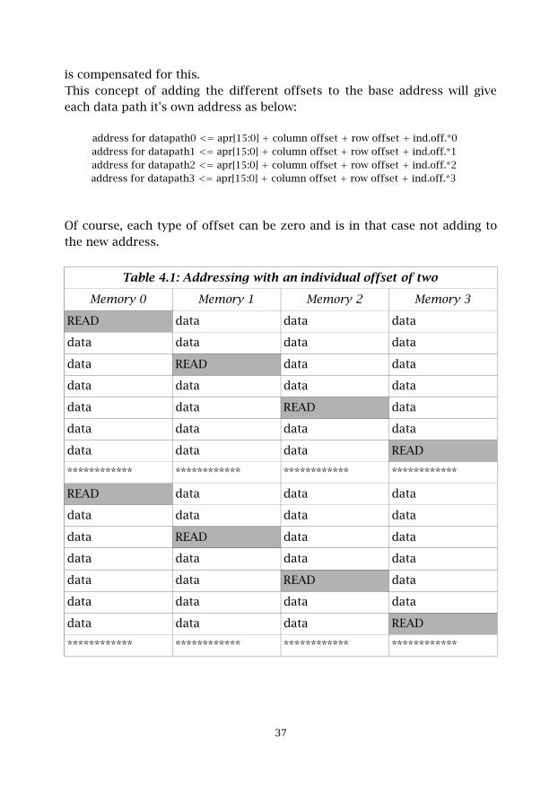
The individual offset works in the way that it multiplies the offset lengthwith the memory number. As an example, see table 4.1 where the individualoffset is two. The length of the individual offset should be configured beforeexecution in the special offset register, IND_OFFSET.
The column offset is an offset with a configurable field length that, togetherwith the row offset, must not be greater than 216. The length of the columnoffset should be configured before execution in the special column register,the COL_OFFSET.
The row offset is a programmable offset that is specified in the instructionword. The length of the row offset differs according to the instruction wordthat is used. When using any table addressing, as memory index addressingfor an example, the width can be up to 16-bits as long as the column offset
��
is compensated for this.This concept of adding the different offsets to the base address will giveeach data path it's own address as below:
address for datapath0 <= apr[15:0] + column offset + row offset + ind.off.*0address for datapath1 <= apr[15:0] + column offset + row offset + ind.off.*1address for datapath2 <= apr[15:0] + column offset + row offset + ind.off.*2address for datapath3 <= apr[15:0] + column offset + row offset + ind.off.*3
Of course, each type of offset can be zero and is in that case not adding tothe new address.
Table 4.1: Addressing with an individual offset of two
Memory 0 Memory 1 Memory 2 Memory 3
READ data data data
data data data data
data READ data data
data data data data
data data READ data
data data data data
data data data READ
************ ************ ************ ************
READ data data data
data data data data
data READ data data
data data data data
data data READ data
data data data data
data data data READ
************ ************ ************ ************
��
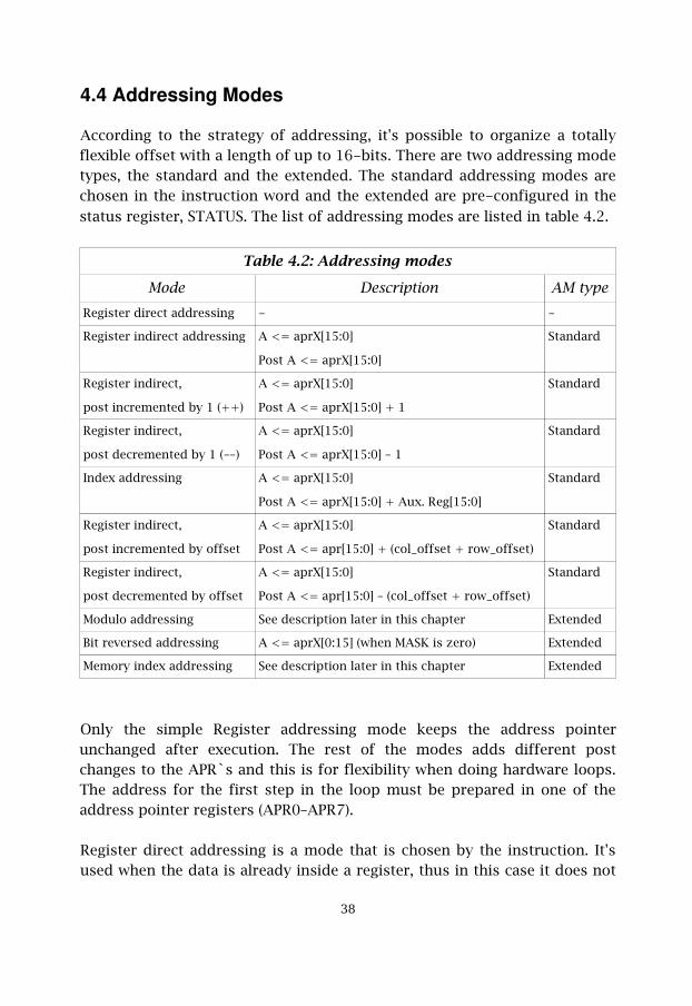
4.4 Addressing Modes
According to the strategy of addressing, it's possible to organize a totallyflexible offset with a length of up to 16-bits. There are two addressing modetypes, the standard and the extended. The standard addressing modes arechosen in the instruction word and the extended are pre-configured in thestatus register, STATUS. The list of addressing modes are listed in table 4.2.
Table 4.2: Addressing modes
Mode Description AM typeRegister direct addressing - -
Register indirect addressing A <= aprX[15:0]
Post A <= aprX[15:0]
Standard
Register indirect,
post incremented by 1 (++)
A <= aprX[15:0]
Post A <= aprX[15:0] + 1
Standard
Register indirect,
post decremented by 1 (––)
A <= aprX[15:0]
Post A <= aprX[15:0] – 1
Standard
Index addressing A <= aprX[15:0]
Post A <= aprX[15:0] + Aux. Reg[15:0]
Standard
Register indirect,
post incremented by offset
A <= aprX[15:0]
Post A <= apr[15:0] + (col_offset + row_offset)
Standard
Register indirect,
post decremented by offset
A <= aprX[15:0]
Post A <= apr[15:0] – (col_offset + row_offset)
Standard
Modulo addressing See description later in this chapter Extended
Bit reversed addressing A <= aprX[0:15] (when MASK is zero) Extended
Memory index addressing See description later in this chapter Extended
Only the simple Register addressing mode keeps the address pointerunchanged after execution. The rest of the modes adds different postchanges to the APR`s and this is for flexibility when doing hardware loops.The address for the first step in the loop must be prepared in one of theaddress pointer registers (APR0–APR7).
Register direct addressing is a mode that is chosen by the instruction. It'sused when the data is already inside a register, thus in this case it does not
��
need to be addressed in the memory.
Register indirect addressing is a mode where we address data that is insidethe memory. The data is found in the memory at the address that is given bythe chosen APR.
Register indirect addressing with post changes such as increment,decrement, plus offset, minus offset and plus index register is used whenthe address in the APR`s must be updated after execution. This is necessaryfor being able to generate the correct addresses when doing hardware loops.
Modulo addressing, or circular addressing that it's also called, is anextended addressing mode that can be used in conjunction with any otherstandard addressing modes. It's very useful when working with circular databuffers. When using Modulo addressing, there must be a TAR, Top AddressRegister, and a BAR, Bottom Address Register, already configured thatspecifies a top and bottom address. When using Modulo addressing inconjunction with another standard addressing mode with post changes andthe address pointer reaches the bottom address, the address flips over tothe top address instead of the next address. In this way the generatedaddresses circulates between the top address and the bottom address andit's because of this it's also called circular addressing. When Moduloaddressing is used the circular addressing is applied to Memory1 andmemory3. Bit-Reversed Addressing, BRA, is also an extended address mode that canbe used in conjunction with any other standard addressing modes. Whenthe address is generated, the BRA inverts the bits according to a pre-configured mask register, MASK. The mask register specifies how manyMSB`s that should not be inverted, thus masked. An example is given intable 4.3.
�
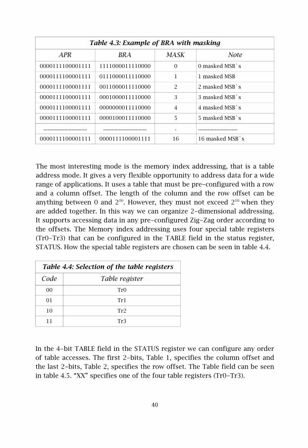
Table 4.3: Example of BRA with masking
APR BRA MASK Note0000111100001111 1111000011110000 0 0 masked MSB`s
0000111100001111 0111000011110000 1 1 masked MSB
0000111100001111 0011000011110000 2 2 masked MSB`s
0000111100001111 0001000011110000 3 3 masked MSB`s
0000111100001111 0000000011110000 4 4 masked MSB`s
0000111100001111 0000100011110000 5 5 masked MSB`s
............................... ............................... . ............................
0000111100001111 0000111100001111 16 16 masked MSB`s
The most interesting mode is the memory index addressing, that is a tableaddress mode. It gives a very flexible opportunity to address data for a widerange of applications. It uses a table that must be pre-configured with a rowand a column offset. The length of the column and the row offset can beanything between 0 and 216. However, they must not exceed 216 when theyare added together. In this way we can organize 2-dimensional addressing.It supports accessing data in any pre-configured Zig-Zag order according tothe offsets. The Memory index addressing uses four special table registers(Tr0-Tr3) that can be configured in the TABLE field in the status register,STATUS. How the special table registers are chosen can be seen in table 4.4.
Table 4.4: Selection of the table registers
Code Table register00 Tr0
01 Tr1
10 Tr2
11 Tr3
In the 4-bit TABLE field in the STATUS register we can configure any orderof table accesses. The first 2-bits, Table 1, specifies the column offset andthe last 2-bits, Table 2, specifies the row offset. The Table field can be seenin table 4.5. “XX” specifies one of the four table registers (Tr0-Tr3).
�(

Table 4.5: Description of the TABLE field
Table1, column Table2, rowb'XX' b'XX'
b'XX' b'XX'
b'XX' b'XX'
b'XX' b'XX'
��

��
5Instruction set design
5.1 Preview
The instruction set is the interface between hardware and software. Theperformance of the DSP is heavily dependent on the instruction set. Aninstruction set must be simple and as orthogonal as possible. If it can behighly orthogonal, then the instruction set is efficient.
The task was to design a set of very few instruction words with instead asmany specifiers as possible. The instruction set for this DSP uses eight 32-bit instruction words.However, we have only used six of them in our design and therefor two ofthem are reserved for future use. The six instruction words that are used areMOVE, ALU, MAC, DMAC, SIMD and P_FLOW.
Because the 32-bit limitation in the instruction words, there is not space forall specifiers that are needed. There have to be some sort of a trade off. Inthis work we concentrated on making the instruction words as flexible aspossible regarding addressing. The trade off for having such a highaddressing flexibility is to use a status register for additional specifiers. Inour design we have used the 16-bit GPR31 as the status register, STATUS.The status register is always checked before execution for pre-configuringthe DSP and is updated after execution. All instruction words are designedto use the status register.
��
5.2 Hardware Description
The hardware architectures for the data paths of this DSP processor areshown in chapter 3. The processor core have six executional units, oneextended mac, the MAC0 containing a serial data path and four parallel datapaths, and MAC1 containing another serial data path.
The data can be accessed in the general purpose registers, GPR0-GPR31, andin the memories, M0-M3. When accessing memories, this is done througheight 16-bit address pointer registers, APR0-APR7, containing memoryaddresses. The APR`s are the same for all data paths. The description of theaddress generation unit, AGU, that is responsible for that the correctaddresses is being generated, is described in chapter 4.
The data can also be stored and accessed in accumulator registers, ACR`s.Each data path have its own set of ACR`s for saving intermediate results.The serial data paths have a set of eight 40-bit accumulator registers each.The parallel data paths don't do the same kind of processing and have nouse of 40-bit precision, and therefor they instead have a set of eight 20-bitaccumulator registers each. This is enough because the most computingintense that can occur in a parallel data path is the multiplication by two 8-bit data.
5.2.1 The STATUS register
When designing our model we decided that the DSP processor's instructionset must be as flexible as possible. However, if everything should be 100percent flexible, then everything must be programmable. If we makeeverything programmable, then the instruction words will be very long. Theinstruction words in our design are limited to 32-bits so a trade off is, asalways, needed. We had to carefully analyze which functions that should beprogrammable and which that instead should be configurable. The functionsthat was decided to be configurable was put into a status register, STATUS.The status register is one of the general purpose registers (GPRs) in theregister file. The GPR31 was chosen as the status register, STATUS.
��
5.2.2 Partitioning between configurable and programmable
The type of the data, if it has integer or fractional representation or if it'ssigned or unsigned, should be known before accessing it in order togenerate the correct control signals. Because of this, the specifiers forselecting it are decided to be configurable and are moved to the statusregister.
When computing with a DSP processor, hardware loops are performedalmost all of the time and the way to handle the data must be known beforeentering the loop. If saturation should be turned on or off, if the data shouldbe rounded and truncated to extract native width and the use of carry orsaturation arithmetic must be known and is therefor moved to the statusregister.
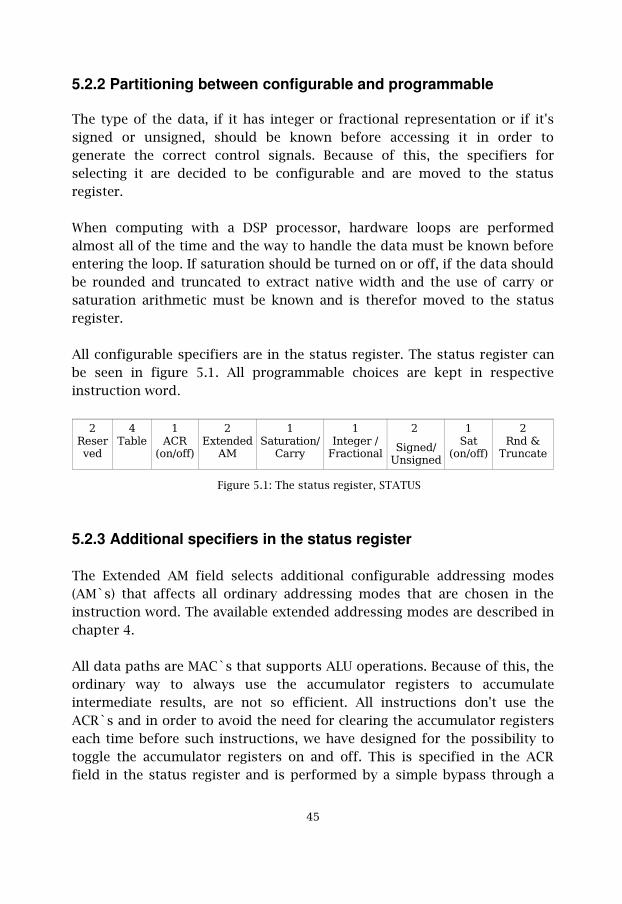
All configurable specifiers are in the status register. The status register canbe seen in figure 5.1. All programmable choices are kept in respectiveinstruction word)
�$����*��
�%� ��
��+$
,��-���.
�/0������
�1
����������-
+����
���������-2�� ������
��
�����-3�������
���
,��-���.
�$���!%��� ���
Figure 5.1: The status register, STATUS
5.2.3 Additional specifiers in the status register
The Extended AM field selects additional configurable addressing modes(AM`s) that affects all ordinary addressing modes that are chosen in theinstruction word. The available extended addressing modes are described inchapter 4.
All data paths are MAC`s that supports ALU operations. Because of this, theordinary way to always use the accumulator registers to accumulateintermediate results, are not so efficient. All instructions don't use theACR`s and in order to avoid the need for clearing the accumulator registerseach time before such instructions, we have designed for the possibility totoggle the accumulator registers on and off. This is specified in the ACRfield in the status register and is performed by a simple bypass through a
��

multiplexer.
The Table field specifies the column and row offset registers. The first 2-bits specifies one of the four table registers (Tr0-Tr3) that should be used asthe column offset and the last 2-bits specifies which of the four tableregisters (Tr0-Tr3) that should be used as the row offset. For a detaileddescription of Table addressing, see Memory index addressing in chapter 4.
The 2-bit reserved field is for future use.
��

5.3 MOVE
During DSP, a lot of time is used for ordering the data such as movingbetween registers, memories etc. This is very time consuming and a lot ofeffort have been made in making the move operations as efficient aspossible. If the DSP processor is very fast at calculations but don't have aneffective move arithmetic, then there is no point with the fast calculations.In this case we will loose cycles when moving and then gain them back whencalculating and the result will be all but impressive.
The complexity of designing the move instruction word increases with thenumber of executional units. In our case with six executional units, tradeoffs are necessary. The chosen design will be explained in detail in thischapter.
5.3.1 MOVE model
Our move instructions supports moving from the two serial data paths orthe four parallel data paths to the four memories. The opposite order, fromthe memories to the serial and the parallel data paths, is of course alsosupported. There is also a possibility to load a 16-bit immediate valuedirectly to the general purpose registers, the address pointer registers or thememories. When moving between parallel data paths and memories allparallel data paths are affected. This means that there is always four valuesthat are moved between the memories and the parallel data paths by onlyone move instruction. The same is true for the dual MAC structure, with twoserial data paths. The only exception is that there are two results generatedinstead of four.
5.3.2 MOVE instruction word
There is always a trade off between programmability and configurability in arelatively short instruction word. All needed specifiers can't be fitted in a32-bit instruction word and therefor it depends on the status register aswell. When moving to memory or general purpose registers it's vital that thedata is 16-bit because of the hardware limitation of 16 bits. However, mostof the time the data is larger than 16 bits because of the much higher
��

internal precision. To solve this problem their is support for converting tonative length. This is decided by the status register, STATUS, that is alwayschecked before execution. The explanation of the status register is in sub-chapter 5.2.
After our research, the instruction word that is seen in figure 5.2 wasdesigned.
�
%���
�
45
�
�1
�
-6
�3������
�����0�$���
�$��
��4�����
��
�7�����
7�+$
�
6$��
�������
��6
�67�����
Figure 5.2: MOVE instruction word
The Type field identifies that it's a move instruction. The OP field decideswhat instruction that should be used. The supported instructions are intable 5.1.
Table 5.1: MOVE instruction listOp Instruction Op Instruction
000 NOP 100 SWP (SWaP data between registers)
001 BMM (Between Memory and Memory) 101 CLA (CLear Accumulator)
010 BRM (Between Register and Memory)110
LD (LoaD register or memory withimmediate data)
011 BRR (Between Register and Register) 111 Reserved
The AM field is described in the addressing part for the move later inchapter 5.3.3.
The S/D field has a multi purpose depending on which instruction that isbeing used. If the instruction is BRM, Between Register and Memory, then it specifies ifthe source is a GPR, a SA, a PA or a memory. A SA is a serial ACR in both
��
MAC0 and MAC1 and the PA is one ACR in each parallel data path. Forexample, if the source is PA0 than, this means that the data in each PA0, inthe parallel data paths, are moved to all memories. In this case, PA0 in datapath0 is moved to memory0 and ACR0 in data path1 is moved to memory1and so on. Both the SA`s and the PA`s are specified in the sourceaccumulator, S_ACR, field.
If the instruction is CLA the S/D field specifies which accumulator thatshould be cleared. It can be an ACR in the serial data path in MAC0, an ACRin the serial data path in MAC1, both ACR`s in both serial data paths or allfour ACR`s in the parallel data paths.
If the instruction instead is LD, then the S/D field specifies if the destinationis a GPR, a APR or a memory.
The Index Reg, index register, field is selected if the addressing mode isindex addressing. The 5-bit Index Reg field specifies one of the 32 GPR`sthat should be used as the index register.
The offset field is selected by the address modes that uses offsets. It's anlarge 11-bit standard offset that is fully programmable in the instructionword and it has nothing to do with column and row offsets.
The Imm16 field is a 16-bit field that is used for immediate address andimmediate data. The LD instruction selects this field. The S/D specifier thendecides if the 16-bit data is an address or data. If S/D specifies the memoryor a GPR, then it's immediate data and if the S/D instead specifies a APR,then it's an immediate address.
The mS and the mD field, each specifies one of the four memories as thesource and the destination. The S_point and D_point, each specifies one ofthe eight APR`s as the source and destination addresses. The Sreg and Dreg,each specifies one of the 32 GPR`s as the source and destination registers.
�
5.3.3 MOVE addressing model
The complete addressing model for this processor is described in chapter 4.
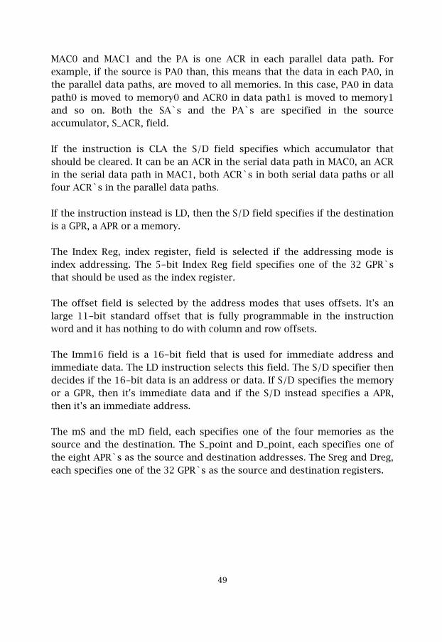
The MOVE model of addressing can be seen as an addressing flow graph.This addressing flow graph is illustrated in figure 5.3.
First, the MOVE instruction word is being read. If the source is in thememory the address to it is generated and the APR is updated, for the nextinstruction cycle, based on the incrementing technique that is currentlybeing used. The data is determined and accessed. Now the MOVE instructionis being executed and finally it starts all over again by reading the nextinstruction.
Figure 5.3: The MOVE addressing flow graph
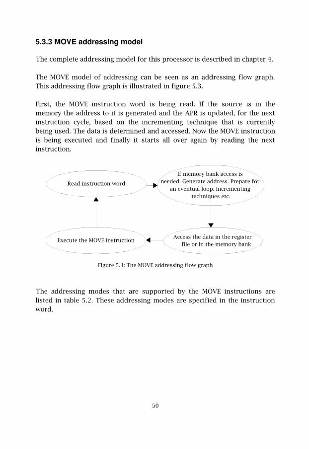
The addressing modes that are supported by the MOVE instructions arelisted in table 5.2. These addressing modes are specified in the instructionword.
�(
Execute the MOVE instruction Access the data in the register file or in the memory bank
If memory bank access is needed. Generate address. Prepare for
an eventual loop. Incrementing techniques etc.
Read instruction word
Table 5.2: MOVE addressing modes
AM Addressing mode Description000 Register indirect A <= aprX[15:0]
001 Register indirect,
post incremented by 1 (++)
A <= aprX[15:0]
Post A <= aprX[15:0] + 1
010 Register indirect,
post decremented by 1 (––)
A <= aprX[15:0]
Post A <= aprX[15:0] – 1
011 Index addressing A <= aprX[15:0]
Post A <= aprX[15:0] + AuxReg[15:0]
100 Register indirect,
post incremented by offset
A <= aprX[15:0]
Post A <= apr[15:0] + offset
101 Register indirect,
post decremented by offset
A <= aprX[15:0]
Post A <= aprX[15:0] – offset
110 Reserved -
111 Reserved -
The MOVE also supports addressing with the extended addressing modesthat can be chosen inside the status register, STATUS. The extendedaddressing modes are used in conjunction with the standard addressingmodes. These modes can be helpful if a lot of data has to be rearranged inthe memories. In this case, there might be a need to loop MOVE instructionsand the extended addressing modes are very useful for this. The supportedextended addressing modes can be seen in table 5.3. The extendedaddressing modes are applicable to all MOVE addressing modes.
Table 5.3: Extended addressing modes
Extended AM Addressing mode Description00 Not used No extended addressing mode
01 Modulo addressing See chapter 4
10 Bit reversed addressing See chapter 4
11 Memory index addressing See chapter 4
��
5.4 ALU The Arithmetic and Logic Unit, ALU, supports the 16-bit logic, arithmeticand shift operations. In order to speed up these operations, this DSPprocessor can execute one logic, one arithmetic and one shift operation inthe same cycle.
The ALU architecture is divided into three blocks that the operandspropagates through. The first block is the logic block, the second is thearithmetic block and the third is the shift block. The only limitation is thatthe order of the blocks are fixed. The order must be, first the logic, secondthe ALU and third the shift operation. However, any block can be disabled ifnot needed. The disabling is done by providing a NOP instruction for thatblock. Research has proved that this fixed order is in fact the order that isneeded in 80 percent of the cases. In those 80 percent, this approachprovides a three times theoretical speed up.
In order to improve performance even further, the instruction word usesone more argument then usual in order to avoid implied addressing in mostcases. By avoiding implied addressing the performance is improved forsome applications. The improvement is caused by the fact that the result isstored at the correct location directly without the need for a MOVEinstruction.
5.4.1 ALU model
All ALU operations are provided by the serial data paths in either MAC0 orMAC1. There is no special ALU unit, instead, each MAC have hardwaresupport for ALU instructions.
The serial data paths can read data from any of the memories or the generalpurpose registers. The computed results can also be written to any memoryor general purpose register. This strategy was chosen because there is oneinstruction cycle saved each time we can avoid a MOVE instruction. In thisway, it's not necessary to execute move instructions to prepare data in thegeneral purpose registers before execution.
The inputs of the serial data paths are 16-bit but internally they are sign or
��
zero extended depending on the operation. Internally all computations are40-bit in order to provide a high precision of the result. The 40-bit resultscan be rounded, saturated and truncated in order to get the 16-bit nativelength at the output.
5.4.2 ALU instruction word
The ALU instruction word is designed so that implied addressing is avoidedin most cases. Implied addressing means that the destination is both thesecond source and the destination. By avoiding this and instead keep twosources and a separate destination we can further improve the performancein most cases. The reason for the improvement in performance is that moveinstructions can be skipped in the cases when the second source is not thesame as the destination.
The configurable specifiers are in the status register, STATUS.
After our research, we designed the instruction word that is in figure 5.4.The dark gray fields are for use with the Register direct modes and the lightgray are for use with the Register indirect modes.
3
Type
3
Logic
5
Arithmetic
3
Shift
3
AM
5SReg1
2mS1
3S_point1
5SReg2
2mS2
3S_point2
5Row offset
Imm10
5S/DReg
2mD/S
3
S/D_point
S/D_ACR
Figure 5.4: ALU instruction word
The Type field identifies that this instruction word is the ALU. The AM fieldspecifies the addressing modes. The addressing modes are described later insub-chapter 5.4.3.
The Logic field specifies the logic instruction. The supported logicinstructions are listed in table 5.4.
��
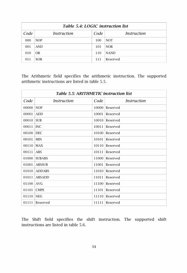
Table 5.4: LOGIC instruction list
Code Instruction Code Instruction000 NOP 100 NOT
001 AND 101 NOR
010 OR 110 NAND
011 XOR 111 Reserved
The Arithmetic field specifies the arithmetic instruction. The supportedarithmetic instructions are listed in table 5.5.
Table 5.5: ARITHMETIC instruction list
Code Instruction Code Instruction00000 NOP 10000 Reserved
00001 ADD 10001 Reserved
00010 SUB 10010 Reserved
00011 INC 10011 Reserved
00100 DEC 10100 Reserved
00101 MIN 10101 Reserved
00110 MAX 10110 Reserved
00111 ABS 10111 Reserved
01000 SUBABS 11000 Reserved
01001 ABSSUB 11001 Reserved
01010 ADDABS 11010 Reserved
01011 ABSADD 11011 Reserved
01100 AVG 11100 Reserved
01101 CMPE 11101 Reserved
01110 NEG 11110 Reserved
01111 Reserved 11111 Reserved
The Shift field specifies the shift instruction. The supported shiftinstructions are listed in table 5.6.
��
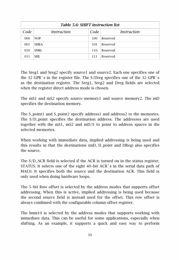
Table 5.6: SHIFT instruction list
Code Instruction Code Instruction000 NOP 100 Reserved
001 SHRA 101 Reserved
010 SHRL 110 Reserved
011 SHL 111 Reserved
The Sreg1 and Sreg2 specify source1 and source2. Each one specifies one ofthe 32 GPR`s in the register file. The S/Dreg specifies one of the 32 GPR`sas the destination register. The Sreg1, Sreg2 and Dreg fields are selectedwhen the register direct address mode is chosen.
The mS1 and mS2 specify source memory1 and source memory2. The mDspecifies the destination memory.
The S_point1 and S_point2 specify address1 and address2 to the memories.The S/D_point specifies the destination address. The addresses are usedtogether with the mS1, mS2 and mD/S to point to address spaces in theselected memories.
When working with immediate data, implied addressing is being used andthis results in that the destinations (mD, D_point and DReg) also specifiesthe source.
The S/D_ACR field is selected if the ACR is turned on in the status register,STATUS. It selects one of the eight 40-bit ACR`s in the serial data path ofMAC0. It specifies both the source and the destination ACR. This field isonly used when doing hardware loops.
The 5-bit Row offset is selected by the address modes that supports offsetaddressing. When this is active, implied addressing is being used becausethe second source field is instead used for the offset. This row offset isalways combined with the configurable column offset register.
The Imm10 is selected by the address modes that supports working withimmediate data. This can be useful for some applications, especially whenshifting. As an example, it supports a quick and easy way to perform
��
scaling.
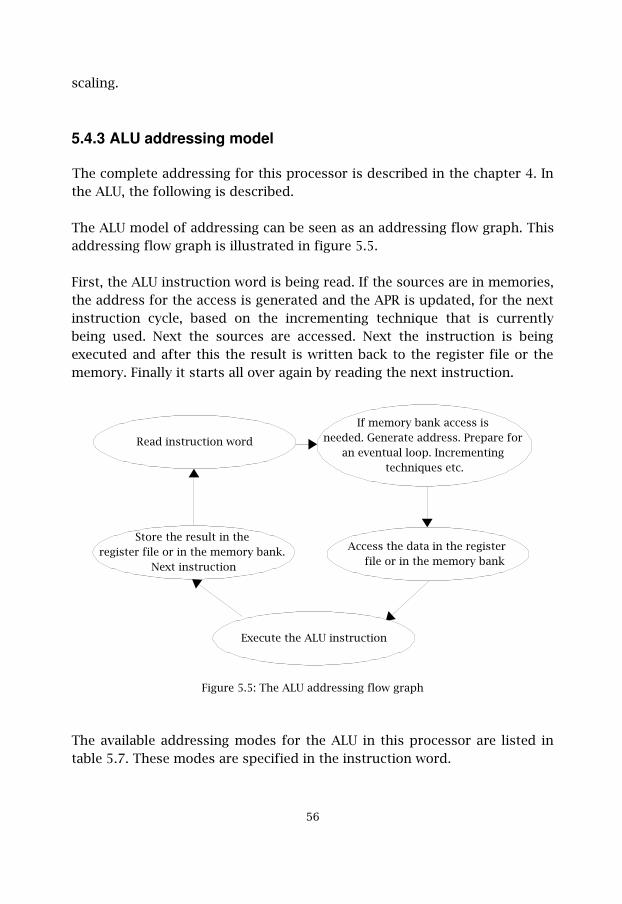
5.4.3 ALU addressing model
The complete addressing for this processor is described in the chapter 4. Inthe ALU, the following is described.
The ALU model of addressing can be seen as an addressing flow graph. Thisaddressing flow graph is illustrated in figure 5.5.
First, the ALU instruction word is being read. If the sources are in memories,the address for the access is generated and the APR is updated, for the nextinstruction cycle, based on the incrementing technique that is currentlybeing used. Next the sources are accessed. Next the instruction is beingexecuted and after this the result is written back to the register file or thememory. Finally it starts all over again by reading the next instruction.
Figure 5.5: The ALU addressing flow graph
The available addressing modes for the ALU in this processor are listed intable 5.7. These modes are specified in the instruction word.
��
Store the result in the register file or in the memory bank.
Next instruction
Execute the ALU instruction
Read instruction word
Access the data in the register file or in the memory bank
If memory bank access is needed. Generate address. Prepare for
an eventual loop. Incrementing techniques etc.

Table 5.7: ALU addressing modes
Code Addressing mode Description000 Register direct No address
001 Register direct
with immediate data
No address
010 Register indirect A <= aprX[15:0]
Post A <= aprX[15:0]
011 Register indirect
with immediate data
A <= aprX[15:0]
Post A <= aprX[15:0]
100 Register indirect,
post incremented by 1 (++)
A <= aprX[15:0]
Post A <= aprX[15:0] + 1
101 Register indirect,
post decremented by 1 (––)
A <= aprX[15:0]
Post A <= aprX[15:0] – 1
110 Register indirect,
post incremented by offset
A <= aprX[15:0]
Post A <= aprX[15:0] + (col_offset + row_offset)
111 Register indirect,
post decremented by offset
A <= aprX[15:0]
Post A <= aprX[15:0] – (col_offset + row_offset)
The ALU also supports addressing with the extended addressing modes thatcan be chosen inside the status register, STATUS. The extended addressingmodes is used in conjunction with the standard addressing modes. Thesupported extended addressing modes can be seen in table 5.3.
��

5.5 MAC
During DSP, most of the calculations are multiply and accumulate whiledoing a hardware loop. These calculations are executed inside a MAC,Multiply and ACcumulate, unit that generates a sum of products, meaningthat the result of the multiplication is always added or subtracted to anACR. These operations are very computing intense and it's often the MACunit that is the bottleneck when measuring the performance.
In order to improve performance, the instruction word uses one moreargument then is usual in order to avoid implied addressing in most cases.By avoiding implied addressing the performance is improved for someapplications. The improvement is caused by the fact that the result is storedat the correct location directly without the use of a MOVE instruction.
5.5.1 MAC model
In the MAC mode the serial data path in MAC0 is used. The serial data pathuses two 16-bit operands. The data can be accessed in two ways. In the firstway, the data are accessed from two memories, one from each memory. Thedescription of the address generation unit, AGU, that is responsible for thatthe correct addresses is being generated, is described in chapter 4. In thesecond way, the data are taken from two registers in the register file.
After the processing, the result can be stored in any of the memories, in anyGPR in the register file or in one of the eight 40-bit ACR`s in the serial datapath. The source ACR is always the same as the destination ACR.
In order to do hardware loops with the MAC, the 16-bit data has to be takenfrom the memories. The design is not limited to this but it's rather pointlessto use the register file for looping because of the limited space in it.
The inputs of the serial data path are 16-bit but internally all computationsare 40-bit in order to provide a high precision of the result. The 40-bitresult can be rounded, saturated and truncated in order to get the 16-bitnative length at the output.
��
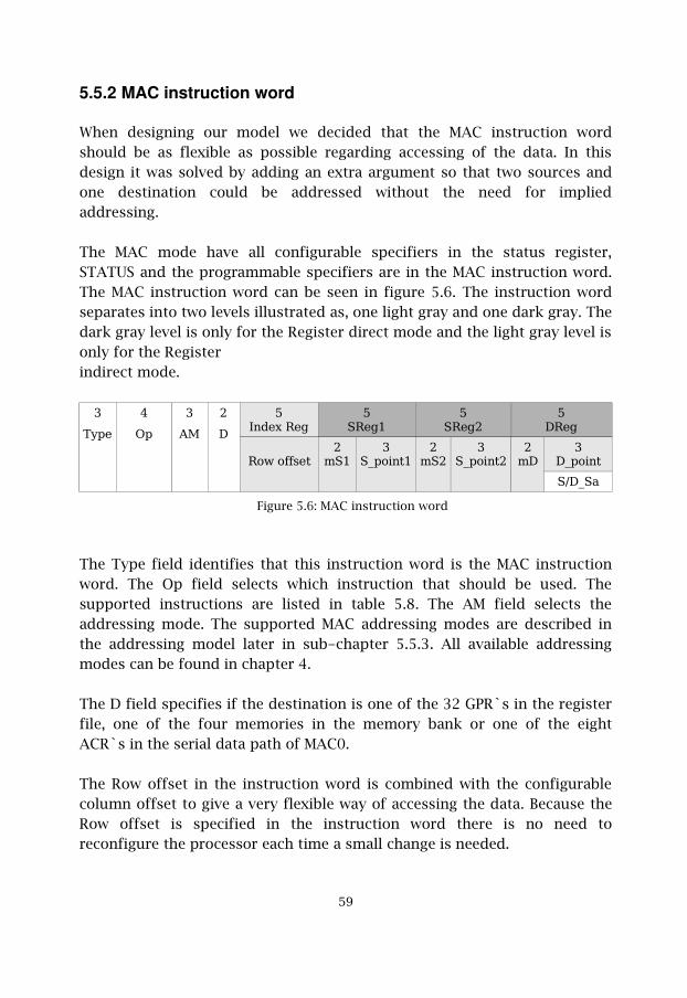
5.5.2 MAC instruction word
When designing our model we decided that the MAC instruction wordshould be as flexible as possible regarding accessing of the data. In thisdesign it was solved by adding an extra argument so that two sources andone destination could be addressed without the need for impliedaddressing.
The MAC mode have all configurable specifiers in the status register,STATUS and the programmable specifiers are in the MAC instruction word.The MAC instruction word can be seen in figure 5.6. The instruction wordseparates into two levels illustrated as, one light gray and one dark gray. Thedark gray level is only for the Register direct mode and the light gray level isonly for the Register indirect mode.
�
%���
�
4�
�
�1
�
6
�����0�$��
�$���
�$���
�6$��
�$�8�������
���
�7������
���
�7������
��6
�67�����
-67�
Figure 5.6: MAC instruction word
The Type field identifies that this instruction word is the MAC instructionword. The Op field selects which instruction that should be used. Thesupported instructions are listed in table 5.8. The AM field selects theaddressing mode. The supported MAC addressing modes are described inthe addressing model later in sub-chapter 5.5.3. All available addressingmodes can be found in chapter 4.
The D field specifies if the destination is one of the 32 GPR`s in the registerfile, one of the four memories in the memory bank or one of the eightACR`s in the serial data path of MAC0.
The Row offset in the instruction word is combined with the configurablecolumn offset to give a very flexible way of accessing the data. Because theRow offset is specified in the instruction word there is no need toreconfigure the processor each time a small change is needed.
�
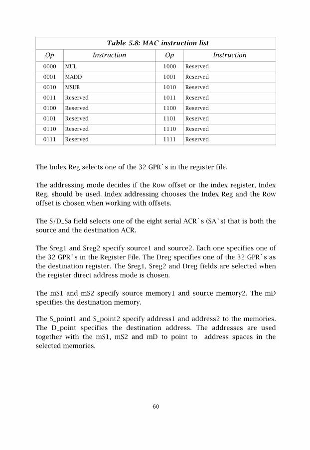
Table 5.8: MAC instruction list
Op Instruction Op Instruction0000 MUL 1000 Reserved
0001 MADD 1001 Reserved
0010 MSUB 1010 Reserved
0011 Reserved 1011 Reserved
0100 Reserved 1100 Reserved
0101 Reserved 1101 Reserved
0110 Reserved 1110 Reserved
0111 Reserved 1111 Reserved
The Index Reg selects one of the 32 GPR`s in the register file.
The addressing mode decides if the Row offset or the index register, IndexReg, should be used. Index addressing chooses the Index Reg and the Rowoffset is chosen when working with offsets.
The S/D_Sa field selects one of the eight serial ACR`s (SA`s) that is both thesource and the destination ACR.
The Sreg1 and Sreg2 specify source1 and source2. Each one specifies one ofthe 32 GPR`s in the Register File. The Dreg specifies one of the 32 GPR`s asthe destination register. The Sreg1, Sreg2 and Dreg fields are selected whenthe register direct address mode is chosen.
The mS1 and mS2 specify source memory1 and source memory2. The mDspecifies the destination memory.
The S_point1 and S_point2 specify address1 and address2 to the memories.The D_point specifies the destination address. The addresses are usedtogether with the mS1, mS2 and mD to point to address spaces in theselected memories.
�(
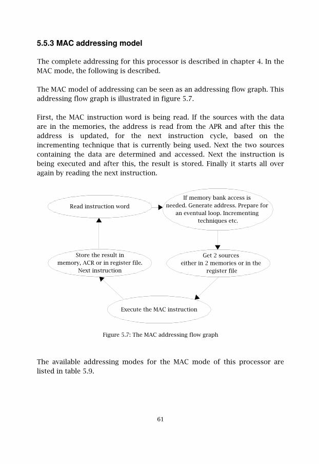
5.5.3 MAC addressing model
The complete addressing for this processor is described in chapter 4. In theMAC mode, the following is described.
The MAC model of addressing can be seen as an addressing flow graph. Thisaddressing flow graph is illustrated in figure 5.7.
First, the MAC instruction word is being read. If the sources with the dataare in the memories, the address is read from the APR and after this theaddress is updated, for the next instruction cycle, based on theincrementing technique that is currently being used. Next the two sourcescontaining the data are determined and accessed. Next the instruction isbeing executed and after this, the result is stored. Finally it starts all overagain by reading the next instruction.
Figure 5.7: The MAC addressing flow graph
The available addressing modes for the MAC mode of this processor arelisted in table 5.9.
��
Store the result in memory, ACR or in register file.
Next instruction
Get 2 sources either in 2 memories or in the
register file
Read instruction word
Execute the MAC instruction
If memory bank access is needed. Generate address. Prepare for
an eventual loop. Incrementing techniques etc.
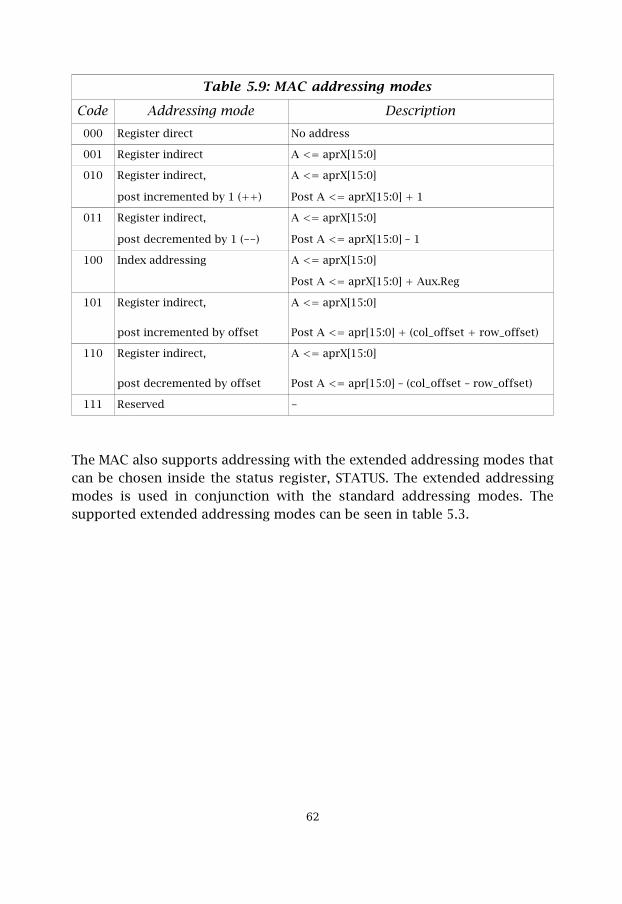
Table 5.9: MAC addressing modes
Code Addressing mode Description000 Register direct No address
001 Register indirect A <= aprX[15:0]
010 Register indirect,
post incremented by 1 (++)
A <= aprX[15:0]
Post A <= aprX[15:0] + 1
011 Register indirect,
post decremented by 1 (--)
A <= aprX[15:0]
Post A <= aprX[15:0] – 1
100 Index addressing A <= aprX[15:0]
Post A <= aprX[15:0] + Aux.Reg
101 Register indirect,
post incremented by offset
A <= aprX[15:0]
Post A <= apr[15:0] + (col_offset + row_offset)
110 Register indirect,
post decremented by offset
A <= aprX[15:0]
Post A <= apr[15:0] – (col_offset – row_offset)
111 Reserved -
The MAC also supports addressing with the extended addressing modes thatcan be chosen inside the status register, STATUS. The extended addressingmodes is used in conjunction with the standard addressing modes. Thesupported extended addressing modes can be seen in table 5.3.
��
5.6 DMAC
As mentioned in the MAC sub-chapter, it's often the MAC that is thebottleneck for performance. In order to improve the performance, thethroughput must be increased. To increase the throughput the DSPprocessor must run at a higher frequency. While it might seem simple to runthe processor at a higher frequency, this is not the solution because thereare hardware limitations on how fast you can run it.
A completely different approach is to add another MAC unit and divide theworkload between the MAC units. In this case the calculations can becompleted in half the time compared to when using only one MAC unit. Thisis the chosen approach in this project.
A dual mac, DMAC, architecture can theoretically improve the performanceby a factor two. However, this is not the case with real world applicationsbecause of problems with the separation of the workload. While it can soundsimple to separate the workload, you can be assured it's not. It's only whenthe workload can be totally separated into two identical parts that we canachieve the two times speed up. In this way the MAC units works completelyindividual and in parallel.
Even if the performance can't be improved by a factor two, it's stillpreferable to have another MAC unit because of the increased performance.The improvement is still better than with one MAC unit.
The DMAC mode can be run simultaneously with the SIMD mode if it usesonly the Register File. This offers a very high parallelism and the greatestperformance that this DSP processor can offer.
5.6.1 DMAC model
In the DMAC mode the two serial data paths of MAC0 and MAC1 are used.Each serial data path uses two operands of 16 bits each. In this design wecan get four operands in two ways. The first is to access all four memoriesat the same time and get one 16-bit operand from each memory. Thesecond is to access four 16-bit GPR`s in the register file. Our register filesupports reading from four different registers at the same time.
��
In order to do hardware loops with the MAC`s, the 16-bit data has to betaken from the memories. The design is not limited to this but it's ratherpointless to use the register file for looping because of the limited space init.�
When using register indirect and thus accessing memories, one base addressis taken from one of the eight 16-bit APR`s. All operands uses the samebase address but different memories. Each serial data path can read twooperands from any of the memories, one operand from each memory. Afterthe processing of the operands, the two results can be stored in twomemories or in the 40-bit ACR`s in each serial data path. The description ofthe address generation unit, AGU, that is responsible for that the correctaddresses is being generated, is described in chapter 4.
When using register direct, four sources are taken from four GPR`s in theregister file. After the processing the results can be stored in two GPR`s inthe register file or in the ACR`s.
If the results are to be stored in two memories, this is done by impliedaddressing meaning that these two are the same as the second sources.When the two results should be stored in the register file, this is also donewith the use of implied addressing and the two result registers are the sameas the second sources. If the results instead should be stored in the ACR`s,then one of the eight ACR`s is selected and the results are written to thisACR in both serial data paths. The source ACR is always the same as thedestination ACR.
The inputs of the serial data paths are 16-bit but internally all computationsare 40-bit in order to provide a high precision of the result. The 40-bitresults can be rounded, saturated and truncated in order to get the 16-bitnative length at the output.
5.6.2 DMAC instruction word
When designing our model we decided that the DMAC mode should be aspowerful as possible but still flexible enough to be able to run in parallelwith the SIMD mode that is described in sub-chapter 5.7. This forced us todesign the instruction word so that the DMAC supports working with both
��
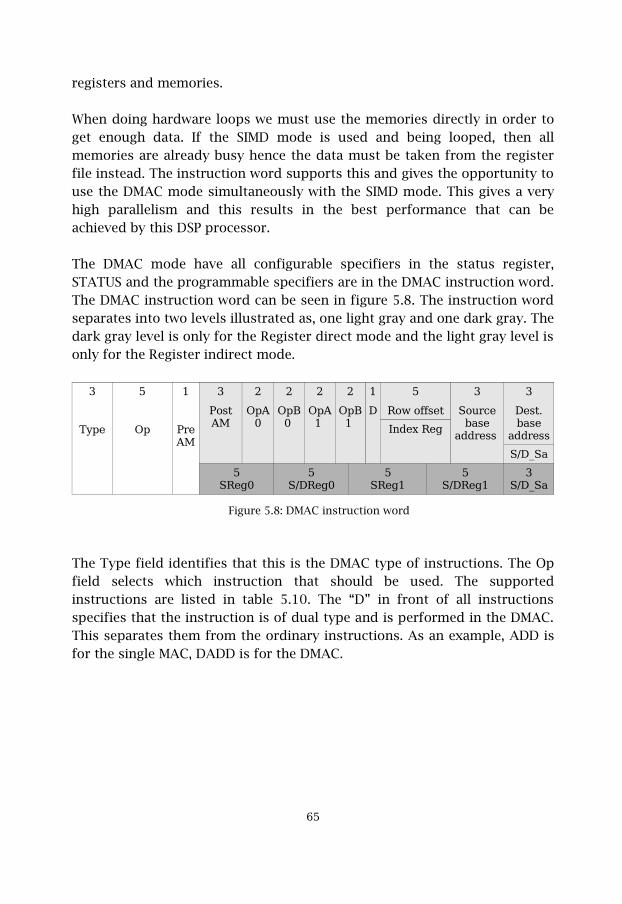
registers and memories.
When doing hardware loops we must use the memories directly in order toget enough data. If the SIMD mode is used and being looped, then allmemories are already busy hence the data must be taken from the registerfile instead. The instruction word supports this and gives the opportunity touse the DMAC mode simultaneously with the SIMD mode. This gives a veryhigh parallelism and this results in the best performance that can beachieved by this DSP processor.
The DMAC mode have all configurable specifiers in the status register,STATUS and the programmable specifiers are in the DMAC instruction word.The DMAC instruction word can be seen in figure 5.8. The instruction wordseparates into two levels illustrated as, one light gray and one dark gray. Thedark gray level is only for the Register direct mode and the light gray level isonly for the Register indirect mode.
�
%���
�
4�
�
5���1
�������
5����1
�
4��(
�
4�"(�
�
4����
�
4�"��
�
6
�
$�8�������
����0�$��
�
��� � ���
��������
�
6���) ���
�������
-67�
�$��(
�-6$��(
�$���
�-6$���
�-67�
Figure 5.8: DMAC instruction word
The Type field identifies that this is the DMAC type of instructions. The Opfield selects which instruction that should be used. The supportedinstructions are listed in table 5.10. The “D” in front of all instructionsspecifies that the instruction is of dual type and is performed in the DMAC.This separates them from the ordinary instructions. As an example, ADD isfor the single MAC, DADD is for the DMAC.
��
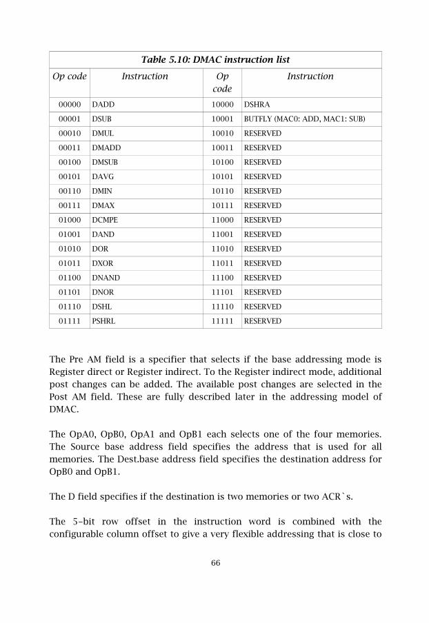
Table 5.10: DMAC instruction list
Op code Instruction Opcode
Instruction
00000 DADD 10000 DSHRA
00001 DSUB 10001 BUTFLY (MAC0: ADD, MAC1: SUB)
00010 DMUL 10010 RESERVED
00011 DMADD 10011 RESERVED
00100 DMSUB 10100 RESERVED
00101 DAVG 10101 RESERVED
00110 DMIN 10110 RESERVED
00111 DMAX 10111 RESERVED
01000 DCMPE 11000 RESERVED
01001 DAND 11001 RESERVED
01010 DOR 11010 RESERVED
01011 DXOR 11011 RESERVED
01100 DNAND 11100 RESERVED
01101 DNOR 11101 RESERVED
01110 DSHL 11110 RESERVED
01111 PSHRL 11111 RESERVED
The Pre AM field is a specifier that selects if the base addressing mode isRegister direct or Register indirect. To the Register indirect mode, additionalpost changes can be added. The available post changes are selected in thePost AM field. These are fully described later in the addressing model ofDMAC.
The OpA0, OpB0, OpA1 and OpB1 each selects one of the four memories.The Source base address field specifies the address that is used for allmemories. The Dest.base address field specifies the destination address forOpB0 and OpB1.
The D field specifies if the destination is two memories or two ACR`s.
The 5-bit row offset in the instruction word is combined with theconfigurable column offset to give a very flexible addressing that is close to
��
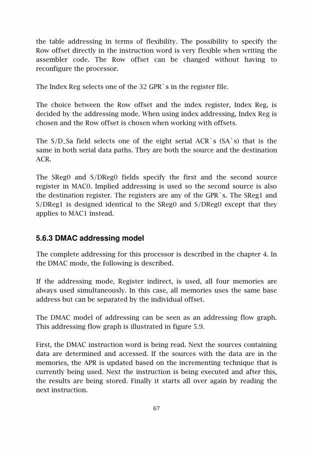
the table addressing in terms of flexibility. The possibility to specify theRow offset directly in the instruction word is very flexible when writing theassembler code. The Row offset can be changed without having toreconfigure the processor.
The Index Reg selects one of the 32 GPR`s in the register file.
The choice between the Row offset and the index register, Index Reg, isdecided by the addressing mode. When using index addressing, Index Reg ischosen and the Row offset is chosen when working with offsets.
The S/D_Sa field selects one of the eight serial ACR`s (SA`s) that is thesame in both serial data paths. They are both the source and the destinationACR.
The SReg0 and S/DReg0 fields specify the first and the second sourceregister in MAC0. Implied addressing is used so the second source is alsothe destination register. The registers are any of the GPR`s. The SReg1 andS/DReg1 is designed identical to the SReg0 and S/DReg0 except that theyapplies to MAC1 instead.
5.6.3 DMAC addressing model
The complete addressing for this processor is described in the chapter 4. Inthe DMAC mode, the following is described.
If the addressing mode, Register indirect, is used, all four memories arealways used simultaneously. In this case, all memories uses the same baseaddress but can be separated by the individual offset.
The DMAC model of addressing can be seen as an addressing flow graph.This addressing flow graph is illustrated in figure 5.9.
First, the DMAC instruction word is being read. Next the sources containingdata are determined and accessed. If the sources with the data are in thememories, the APR is updated based on the incrementing technique that iscurrently being used. Next the instruction is being executed and after this,the results are being stored. Finally it starts all over again by reading thenext instruction.
��
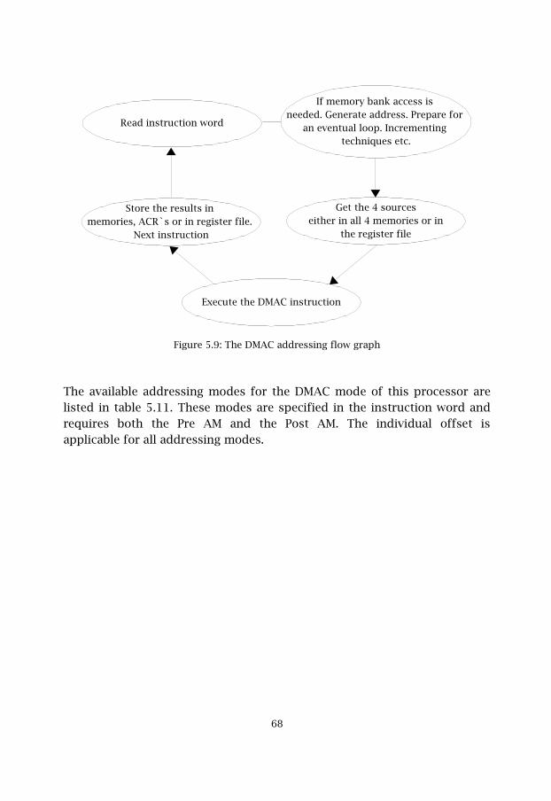
Figure 5.9: The DMAC addressing flow graph
The available addressing modes for the DMAC mode of this processor arelisted in table 5.11. These modes are specified in the instruction word andrequires both the Pre AM and the Post AM. The individual offset isapplicable for all addressing modes.
��
Store the results in memories, ACR`s or in register file.
Next instruction
Get the 4 sources either in all 4 memories or in
the register file
Read instruction word
Execute the DMAC instruction
If memory bank access is needed. Generate address. Prepare for
an eventual loop. Incrementing techniques etc.
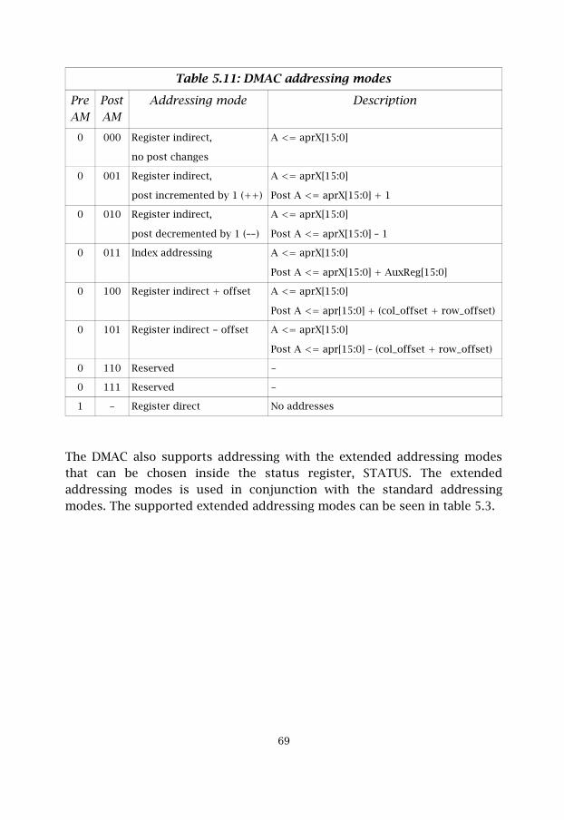
Table 5.11: DMAC addressing modes
PreAM
PostAM
Addressing mode Description
0 000 Register indirect,
no post changes
A <= aprX[15:0]
0 001 Register indirect,
post incremented by 1 (++)
A <= aprX[15:0]
Post A <= aprX[15:0] + 1
0 010 Register indirect,
post decremented by 1 (––)
A <= aprX[15:0]
Post A <= aprX[15:0] – 1
0 011 Index addressing A <= aprX[15:0]
Post A <= aprX[15:0] + AuxReg[15:0]
0 100 Register indirect + offset A <= aprX[15:0]
Post A <= apr[15:0] + (col_offset + row_offset)
0 101 Register indirect - offset A <= aprX[15:0]
Post A <= apr[15:0] – (col_offset + row_offset)
0 110 Reserved -
0 111 Reserved -
1 - Register direct No addresses
The DMAC also supports addressing with the extended addressing modesthat can be chosen inside the status register, STATUS. The extendedaddressing modes is used in conjunction with the standard addressingmodes. The supported extended addressing modes can be seen in table 5.3.
�
5.7 SIMD
In order to speed up media applications we have the ability to use theprocessor in a SIMD mode. SIMD stands for Single Instruction Multiple Data.Media applications, such as MPEG and JPEG for example, are verycomputational intensive and requires the processor to work with a verylarge amount of 8-bit data. In order to address this problem, the processorhave four parallel data paths that are optimized for running mediaapplications in parallel. This requires that the 8-bit data are prepared in thememory as two 8-bit data in one 16-bit space. In this way we can access upto 8 operands, 64 bits of data in one clock cycle. Up to four computationscan be run in parallel with a four times theoretical speed up in the best case.
The parallel data paths are not limited to 8-bits and can be used in twoconfigurations, the dual 8-bit mode and the single 16-bit mode. In the dual8-bit mode, the data must be prepared in the memories but this is notneeded in the 16-bit mode. In the 16-bit mode, multiplications are notsupported in the parallel data paths.
Media applications that requires the processor to work with a large amountof 16-bit data can be accelerated in the parallel data paths, if the 16-bitmode is chosen or in the dual MAC structure. If 16-bit multiplications areneeded then the calculations must be done in the dual MAC structure. Thedual MAC structure will then work as a 16-bit SIMD mode. This mode ofoperation is explained in sub-chapter 5.6.
The SIMD mode can be run simultaneously with the DMAC mode if theDMAC uses only the register file. This offers a very high parallelism and thegreatest performance that this DSP processor can offer.
5.7.1 SIMD model
In the SIMD mode we only use the four parallel data paths in MAC0 foracceleration of media applications. The parallel data paths are alwaysaccessing the memories directly. The register file is never used. The serialdata paths can work in parallel with the parallel data paths as long as theydon't interfere with the memory accesses of the parallel data paths. If thedata is prepared in such a way that the serial data paths can use the register
�(
file most of the time, while the parallel data paths uses the memories, then avery high performance could be achieved.
The parallel data paths access the memories through the use of eight 16-bitaddress pointer registers for memory addresses. The description of theaddress generation unit, AGU, that is responsible for that the correctaddresses is being generated, is described in chapter 4. There is also apossibility to access eight 20-bit accumulator registers for each parallel datapath for saving intermediate results.
Each parallel data path can read from any memory in the memory bankwhen operating in the 8-bit mode. When operating in the 16-bit mode, eachparallel data path reads one operand from the same memory number as thedata path number and the second operand it can get from any memory. Asan example p_dp0 reads from memory0 and from memory 1, 2 or 3. In thisway we access eight operands with only four sources. When writing to thememory the memories are divided such that each parallel data path alwayswrite back to the same memory numbers as data path number. As anexample, parallel data path0 writes to memory0.
The parallel data paths can accept 8-bit or 16-bit data as input, butinternally all computations have 20-bit precision. The 20-bit results can berounded, saturated and truncated in order to get the 16-bit native length atthe output.
5.7.2 SIMD instruction word
When designing our model we decided that the SIMD mode should be asflexible as possible. However, this was not possible because of the limitationof space in the instruction word. The trade off that was necessary to makewas to use a status register, STATUS, and instead put all our effort onmaking the addressing as flexible and powerful as possible. The result isthat we can access 16-bit data in any way including any kind of Zig-Zag likepatterns.
The SIMD instruction word only uses register indirect addressing modes andis because of this, like in the previous sub-chapters, illustrated as light gray.The SIMD mode only uses memories and never the Register File.
��
The programmable part is put directly into the SIMD instruction word, seefigure 5.10.
�
%���
�
4��������
�
�1
�
�5
�
1�4
�
6
�
$�8�������
����0�$��
�
��� � ���
��������
�
6���)� ����������
-675�
Figure 5.10: SIMD instruction word
The design for an addressing that is as flexible as possible gives the demandthat each data path should be able to read from any memory with anoptional offset for the base address source. The addressing modes, AM`s,for the SIMD mode are described later in this sub-chapter. All availableaddressing modes can be found in chapter 4.
The IP field specifies the Input Precision and it can be 8 bits or 16 bits.When the input precision is 8 bits, each 16-bit memory space is seen as 2 x8 bits operands.
�4���������
�4��������
A 16-bit memory space when IP is 8 bits
When the input precision instead is 16-bit, each 16-bit memory space isseen in the regular way as a 1 x 16-bit operand.
��4��������
A 16-bit memory space when IP is 16 bits
The MAO, Memory Access Order, field describes in which order the paralleldata paths are accessing the memories in the memory bank. It worksdifferent according to the input precision bit.
If the input precision bit is 8 bits, then the first 2 bits selects which memorydata path0 should access, the next 2 bits selects which memory data path1should access, the next 2 bits selects which memory data path2 should
��
access and finally the last 2 bits selects which memory data path3 shouldaccess.
Sometimes there might not be a need for all four data paths in thecomputations. This processor supports the use of one or up to four datapaths. If a data path wants to access a memory that is already accessed byanother data path, then the data path is instead disabled. Some examples forthe 8-bit mode are given in table 5.12.
Table 5.12: Data path enabling via MAO when using the 8-bit mode
MAO(dp0,dp1,dp2,dp3)
M# M# M# M#
dp0
dp1
dp2
dp3
Description
00 01 10 11 on on on on dp0 access M0, dp1 access M1, dp2 access M2, dp3access M3
00 01 10 10 on on on off dp0 access M0, dp1 access M1, dp2 access M2
00 01 10 00 on on on off dp0 access M0, dp1 access M1, dp2 access M2
00 01 01 10 on on off off dp0 access M0, dp1 access M1, dp3 accessM2
00 00 00 10 on off off on dp0 access M0, dp3 access M2
01 01 01 01 on off off off dp0 access M1
Some examples for the 16-bit mode are given in table 5.13
Table 5.13: Data path enabling via MAO when using the 16-bit mode
MAO(dp0,dp1,dp2,dp3)
M# M# M# M#
dp0
dp1
dp2
dp3
Description
00 01 10 11 off off off off All dp`s are disabled
01 10 11 00 on on on on dp0 access M0 & M1, dp1 access M1 & M2, dp2 accessM2 & M3, dp3 access M3 & M0
00 10 10 00 off on off on dp1 access M1 & M2, dp3 access M3 & M0
The number of used data paths are always checked and if there is a memory,or more than one, that are not currently being used, the serial data paths
��
will be granted access, if needed.
The D field specifies if the destination is a memory or a parallel accumulatorregister, Pa. The source ACR is always the same as the destination ACR. Itwas designed in this way to provide easy looping. When a parallel ACR isselected, it specifies all four ACR`s. If Pa0 is selected this means Pa0 in allparallel data paths. The accumulation with the ACR`s can be turned off inthe status register, STATUS. This is useful when performing ALUinstructions.
There is a 5-bit row offset in the instruction word that can be combinedwith the configurable column offset to give a very flexible addressing that isclose to table addressing in terms of flexibility. The decision to keep the rowoffset in the instruction word is based on that a very a little offset, the rowoffset, is used a lot and is really flexible from the programmers point ofview to have in the instruction word.
The choice between the Row offset and the index register, Index Reg, fieldsis decided by the addressing mode. When using index addressing, Index Regis chosen and the Row offset is chosen when working with offsets. TheIndex Reg specifies one of the 32 GPR`s in the Register File.
The base address gives an address that are the same in each memory. TheACR field specifies one of the eight accumulator registers in each paralleldata path. The operation field describes the operations that are supported.Type is the identification of this instruction word for SIMD operations.
All supported SIMD instructions that uses this instruction word are listed intable 5.14. The “P” in all instructions stands for parallel and is only there fordifferentiating between the standard ADD. As an example, PADD meansparallel add. There are 15 reserved instructions for future use.
��
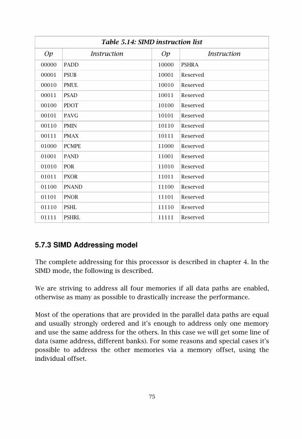
Table 5.14: SIMD instruction list
Op Instruction Op Instruction00000 PADD 10000 PSHRA
00001 PSUB 10001 Reserved
00010 PMUL 10010 Reserved
00011 PSAD 10011 Reserved
00100 PDOT 10100 Reserved
00101 PAVG 10101 Reserved
00110 PMIN 10110 Reserved
00111 PMAX 10111 Reserved
01000 PCMPE 11000 Reserved
01001 PAND 11001 Reserved
01010 POR 11010 Reserved
01011 PXOR 11011 Reserved
01100 PNAND 11100 Reserved
01101 PNOR 11101 Reserved
01110 PSHL 11110 Reserved
01111 PSHRL 11111 Reserved
5.7.3 SIMD Addressing model
The complete addressing for this processor is described in chapter 4. In theSIMD mode, the following is described.
We are striving to address all four memories if all data paths are enabled,otherwise as many as possible to drastically increase the performance.
Most of the operations that are provided in the parallel data paths are equaland usually strongly ordered and it's enough to address only one memoryand use the same address for the others. In this case we will get some line ofdata (same address, different banks). For some reasons and special cases it'spossible to address the other memories via a memory offset, using theindividual offset.
��
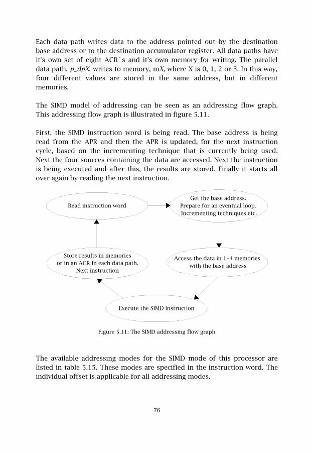
Each data path writes data to the address pointed out by the destinationbase address or to the destination accumulator register. All data paths haveit's own set of eight ACR`s and it's own memory for writing. The paralleldata path, p_dpX, writes to memory, mX, where X is 0, 1, 2 or 3. In this way,four different values are stored in the same address, but in differentmemories.
The SIMD model of addressing can be seen as an addressing flow graph.This addressing flow graph is illustrated in figure 5.11.
First, the SIMD instruction word is being read. The base address is beingread from the APR and then the APR is updated, for the next instructioncycle, based on the incrementing technique that is currently being used.Next the four sources containing the data are accessed. Next the instructionis being executed and after this, the results are stored. Finally it starts allover again by reading the next instruction.
Figure 5.11: The SIMD addressing flow graph
The available addressing modes for the SIMD mode of this processor arelisted in table 5.15. These modes are specified in the instruction word. Theindividual offset is applicable for all addressing modes.
��
Store results in memories or in an ACR in each data path.
Next instruction
�ccess the data in 1-4 memories with the base address
Get the base address. Prepare for an eventual loop. Incrementing techniques etc.
Read instruction word
Execute the SIMD instruction
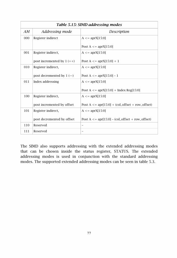
Table 5.15: SIMD addressing modes
AM Addressing mode Description000 Register indirect A <= aprX[15:0]
Post A <= aprX[15:0]
001 Register indirect,
post incremented by 1 (++)
A <= aprX[15:0]
Post A <= aprX[15:0] + 1
010 Register indirect,
post decremented by 1 (––)
A <= aprX[15:0]
Post A <= aprX[15:0] – 1
011 Index addressing A <= aprX[15:0]
Post A <= aprX[15:0] + Index Reg[15:0]
100 Register indirect,
post incremented by offset
A <= aprX[15:0]
Post A <= apr[15:0] + (col_offset + row_offset)
101 Register indirect,
post decremented by offset
A <= aprX[15:0]
Post A <= apr[15:0] – (col_offset + row_offset)
110 Reserved -
111 Reserved -
The SIMD also supports addressing with the extended addressing modesthat can be chosen inside the status register, STATUS. The extendedaddressing modes is used in conjunction with the standard addressingmodes. The supported extended addressing modes can be seen in table 5.3.
��

5.8 PROGRAM FLOW
In order to control the instruction flow in the program memory of the DSPprocessor, program flow instructions are needed. The program flowinstructions are responsible for jumping to addresses in the programmemory and, in the case of a a subroutine jump, also the return to theaddress before the jump. The repeat instruction, for making hardware loops,is also a program flow instruction.
There is not much improvements that can be done in the program flow inorder to increase the executional performance. We instead made theprogram flow as simple and easy to use as possible.
5.8.1 Program flow model
The program flow instructions affects the program counter, PC, in the 64kWprogram memory. They simply control in what order the instructions arebeing executed.
There are three different types of jumps. The first is the ordinary jump thatjumps to a new program memory address. The second is a conditional jumpthat is executed only if the condition is fulfilled. The third is a subroutinejump which executes in the same way as the ordinary jump except that theinternal statuses of the processor are saved. The address is pushed to a PCstack and this stack is then pulled when the return instruction occurs.
Most DSP processors have a repeat instruction and a loop instruction. Whilethese instructions are very similar in their executions, we have designed asimple repeat instruction that supports both repeating and looping. Therepeat instruction take two arguments as input, the number of instructionsthat should be repeated and the number of loops that should be performed.This results in only one repeat instruction that is as easy to use forrepeating one instruction as it is to repeat multiple instructions and providea hardware loop.
��
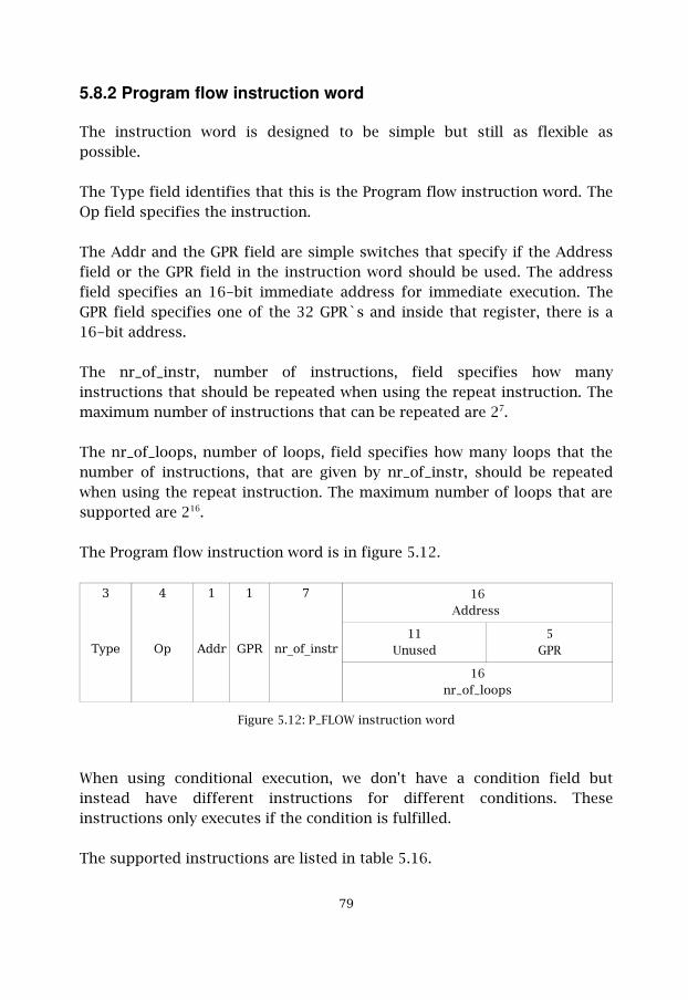
5.8.2 Program flow instruction word
The instruction word is designed to be simple but still as flexible aspossible.
The Type field identifies that this is the Program flow instruction word. TheOp field specifies the instruction.
The Addr and the GPR field are simple switches that specify if the Addressfield or the GPR field in the instruction word should be used. The addressfield specifies an 16-bit immediate address for immediate execution. TheGPR field specifies one of the 32 GPR`s and inside that register, there is a16-bit address.
The nr_of_instr, number of instructions, field specifies how manyinstructions that should be repeated when using the repeat instruction. Themaximum number of instructions that can be repeated are 27.
The nr_of_loops, number of loops, field specifies how many loops that thenumber of instructions, that are given by nr_of_instr, should be repeatedwhen using the repeat instruction. The maximum number of loops that aresupported are 216.
The Program flow instruction word is in figure 5.12.
�
%���
�
4�
�
����
�
95$
�
��7��7�����
16Address
11Unused
5GPR
16nr_of_loops
Figure 5.12: P_FLOW instruction word
When using conditional execution, we don't have a condition field butinstead have different instructions for different conditions. Theseinstructions only executes if the condition is fulfilled.
The supported instructions are listed in table 5.16.
�
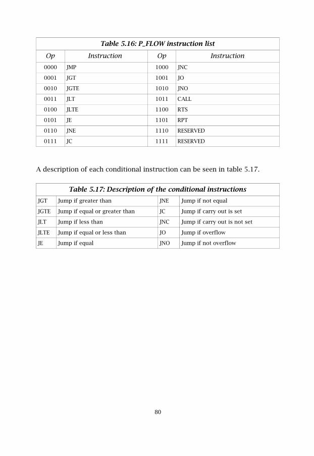
Table 5.16: P_FLOW instruction list
Op Instruction Op Instruction0000 JMP 1000 JNC
0001 JGT 1001 JO
0010 JGTE 1010 JNO
0011 JLT 1011 CALL
0100 JLTE 1100 RTS
0101 JE 1101 RPT
0110 JNE 1110 RESERVED
0111 JC 1111 RESERVED
A description of each conditional instruction can be seen in table 5.17.
Table 5.17: Description of the conditional instructionsJGT Jump if greater than JNE Jump if not equal
JGTE Jump if equal or greater than JC Jump if carry out is set
JLT Jump if less than JNC Jump if carry out is not set
JLTE Jump if equal or less than JO Jump if overflow
JE Jump if equal JNO Jump if not overflow
�(
6Assembler Design
6.1 Preview
When the structure of the instruction set is defined it's time for itsimplementation and verification. It is a very important part of the processordesign flow because it shows if the specification requirements are fulfilledor not. The task is in the translation of the input code (assembly code) to thehexadecimal machine code suitable for this processor. For some reasons thisprocess could be named a compiler design. This chapter is aimed not onlyon the detailed description of this compiler but also on the tools that havebeen used during implementation. According to the design specification wehave followed the IEEE STD 649-1985 standard to design the assembly codeformat.
6.2 Tools Description
To design the language translator of assembly code to hexadecimal code wehave chosen the LEX & YACC tools. The language translator is a programwhich translates programs that are written in a source language into anequivalent program in an objective language. In our case the sourcelanguage is the designed assembly code, the object language is the machinecode of an actual processor. From the pragmatic point of view, thetranslator defines the semantics of the source language, it transformsoperations specified by the syntax into operations of the computationalmodel, into binary control code in our case. Then, the simulator which hasbeen written especially for this reason, will read this binary code andgenerate the corresponding control signals. For a detailed description of thedesigned instruction set simulator, refer to chapter 7 of this document.
��
We have designed a compiler, a translator with a source assembly code andwith the object machine binary code. The typical compiler consists ofseveral stages:
� The lexical stage (so-called scanner) groups characters into lexical unitsor tokens. The input to the lexical stage is a character stream, and theoutput is the stream of tokens. Regular expressions are used to definethe tokens recognized by the scanner. The scanner is implemented as afinite state machine. Lex is a tool for generating scanner. In this work wehave used FLEX, it's a fast version of Lex, working within GNU. They areabsolutely identical from the coding point of view. Here and after allreferences will be on the Flex tool.
� The parser stage groups tokens into syntactical units. The output of theparser is a parse tree representation of the program. Context-freegrammars are used to define the program structure recognized by aparser. The parser is implemented as a push down automate [5]. Yacc is atool that generates the parser. Same as with the Flex we have used theaccelerated version of the Yacc tool. Here we have BISON tool. Bison toolis working withing the GNU too. We will refer here and after to Bison tool.
� The semantic analysis stage analyze the parse tree for context-sensitiveinformation and generates an output as an annotated parse tree. Duringthe parsing, information concerning variables and other objects is storedin the so-called symbol tables.
� The code generator stage transforms the annotated parse tree into objectcode using rules which denote the semantics of the source language.
� Finally, build-in optimizers examine the object code for some dependentmachine improvements.
By using Flex & Bison it's becoming much easier to design the requiredcompiler. During the design of the assembler we tried to do it in a way thatwould be as easy as possible for fast and simple changes in the assemblerstructure. These changes can take place in the future during the debug andverification stages of the instruction set. The compiler design flow is shownin figure 6.1.
��
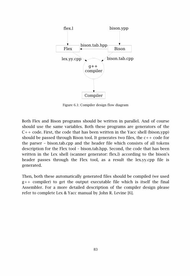
Figure 6.1: Compiler design flow diagram
Both Flex and Bison programs should be written in parallel. And of courseshould use the same variables. Both these programs are generators of theC++ code. First, the code that has been written in the Yacc shell (bison.ypp)should be passed through Bison tool. It generates two files, the c++ code forthe parser – bison.tab.cpp and the header file which consists of all tokensdescription for the Flex tool – bison.tab.hpp. Second, the code that has beenwritten in the Lex shell (scanner generator: flex.l) according to the bison'sheader passes through the Flex tool, as a result the lex.yy.cpp file isgenerated.
Then, both these automatically generated files should be compiled (we usedg++ compiler) to get the output executable file which is itself the finalAssembler. For a more detailed description of the compiler design pleaserefer to complete Lex & Yacc manual by John R. Levine [6].
��
����)������0)�
����)�� )���
��0)��) ��� ����)�� ) ��
2��0 "����
�::� �������
+�������
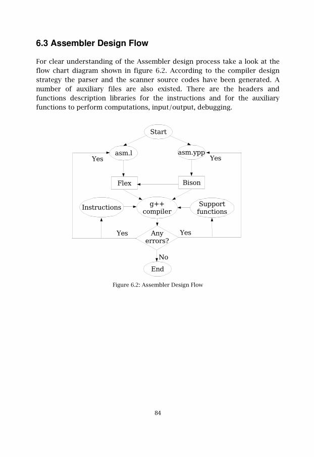
6.3 Assembler Design Flow
For clear understanding of the Assembler design process take a look at theflow chart diagram shown in figure 6.2. According to the compiler designstrategy the parser and the scanner source codes have been generated. Anumber of auxiliary files are also existed. There are the headers andfunctions description libraries for the instructions and for the auxiliaryfunctions to perform computations, input/output, debugging.
Figure 6.2: Assembler Design Flow
��
2��0 "����
���)� ���)���
�:: �������
������ �������������� �����
����
/��
����������;
<�
=��
=��
=��
=��
6.4 Assembler Features
During the research we have found that it's really necessary to design such aflexible structure and processor architecture as possible. A lot of problemsand troubleshooting have occurred during this design stage. For examplethe assembler design causes many problems with the sizing of the datafields in the instruction words, some structures or ideas could not even beimplemented because of the coding style. With increasing of experience inthe instruction set design we had to change some of the alreadyimplemented and workable parts. The additional trouble causes the fact thatwe have to verify both scanner and parser at the same time and some designideas even were canceled, only because of an unideal code style. Forexample, the limitation of number of specifiers in the instruction word.
The final version of the scanner/parser code is really open for adding extraspecifiers into the instruction word or whatever the programmer or designerwants. The main idea is in simplicity of the scanner code. Now there are onlythree main structures in the assembly code to detect (to scan). They are a“number”, an “identifier” and a “char”. Actually, we do not need any moreand can describe any of the assembler specifiers:
� label – is an identifier specified strongly in the beginning of the assemblyline, for example:loopbegin
� mnemonic – is a possible identifier like add, and, or nop. Theseidentifiers must not be in the begin of the line
� argument – could be described with the help of an identifier structure or anumber structure
� flag - is a possible identifier. They have not been used in this instructionset, but it's possible to implement them
� immediate data – is a number structure of data, possible to berepresented via the decimal, binary, octal, or hexadecimal format:15, '1111', 'F'
��
� any other characters
The rest computations and allocations of the data are made with the help ofsupport functions. Data are taken from the symbol tables and theinstruction description header does also exist. This makes the future workwith this scanner/parser much easier for updating and for changing.
6.5 Results
To show the abilities and relative advantages of this processor three types ofinstructions have been implemented for compilation, MOVE instructions,Program Flow instructions, and SIMD instructions. The rest types ofinstructions unfortunately have not been implemented yet because of thetime deficit. But this set of implemented instructions let us check andsimulate this processor using the SIMD data paths.
As a result of compilation the output (for instance “input.hex”) hexadecimalfile is generated if there were no errors or warnings. The Instruction SetSimulator is getting the hex file and doing its job.
��

7Instruction Set Simulator
7.1 Preview
The simulator model is an instruction set simulator, ISS, and is implementedin C++. This programming language was chosen because it's widely taughtand understood. It's easy to work with and good results can be achievedpretty fast. If any questions occurs, it's always easy to find the answers inbooks and on Internet because C++ is so widely spread and used that thereare always somebody else before you that have had the same problems.However, there might be better to use another programming language thathas better support for binary programming because this is C++ biggestflaw.
The task of the ISS is to read 32-bit binary instructions from the programmemory, disassemble them to a readable form, execute the instructions anddo any post processing such as writing back results. Finally the nextinstruction is being read from the program memory and it starts all overagain.
All processing cycles are counted and are printed to the screen in the end.The ISS counts program cycles and executional cycles that takes the pipelineinto account. This is useful for benchmarking different simulator programssuch as FIR, DCT, FFT as some examples.
7.2 Simulator Model
The ISS can copy hex files, that is generated by the Assembler, to theprogram memory. It can copy it to any memory address inside the program
��
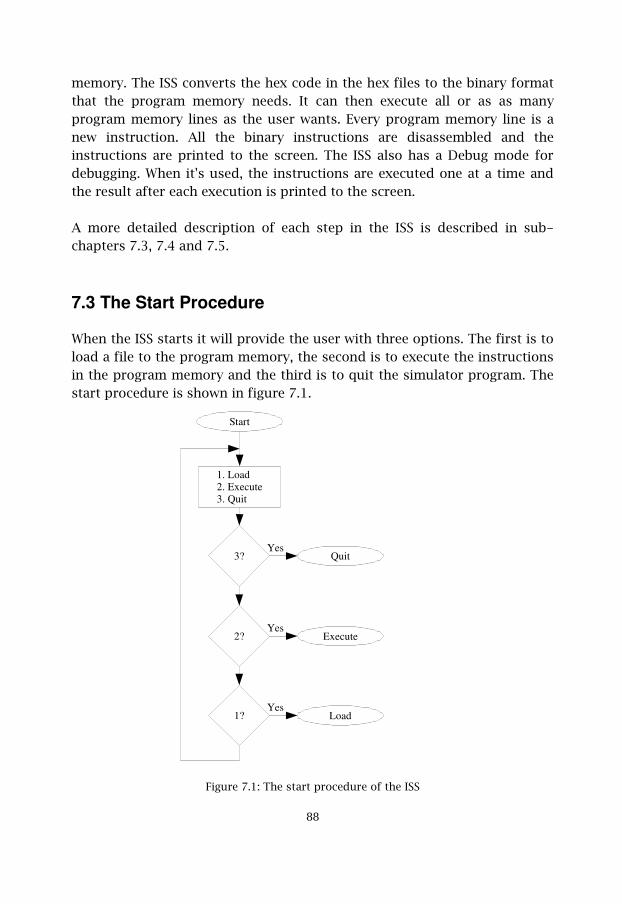
memory. The ISS converts the hex code in the hex files to the binary formatthat the program memory needs. It can then execute all or as as manyprogram memory lines as the user wants. Every program memory line is anew instruction. All the binary instructions are disassembled and theinstructions are printed to the screen. The ISS also has a Debug mode fordebugging. When it's used, the instructions are executed one at a time andthe result after each execution is printed to the screen.
A more detailed description of each step in the ISS is described in sub-chapters 7.3, 7.4 and 7.5.
7.3 The Start Procedure
When the ISS starts it will provide the user with three options. The first is toload a file to the program memory, the second is to execute the instructionsin the program memory and the third is to quit the simulator program. Thestart procedure is shown in figure 7.1.
Figure 7.1: The start procedure of the ISS
��
Start
1. Load2. Execute3. Quit
3?Yes
Quit
2?Yes
Execute
1?Yes
Load
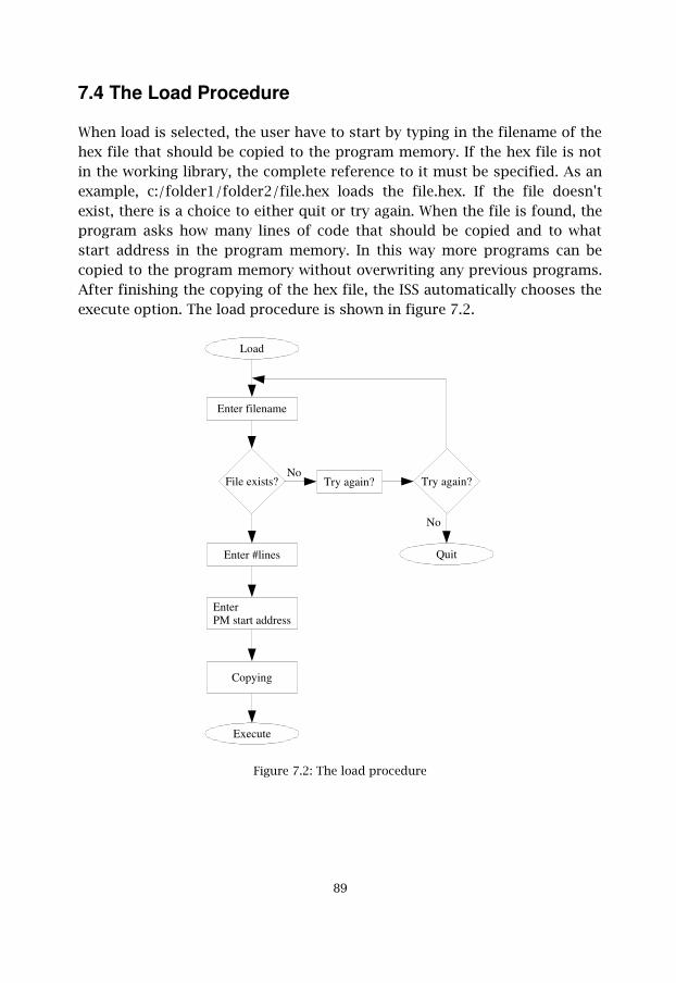
7.4 The Load Procedure
When load is selected, the user have to start by typing in the filename of thehex file that should be copied to the program memory. If the hex file is notin the working library, the complete reference to it must be specified. As anexample, c:/folder1/folder2/file.hex loads the file.hex. If the file doesn'texist, there is a choice to either quit or try again. When the file is found, theprogram asks how many lines of code that should be copied and to whatstart address in the program memory. In this way more programs can becopied to the program memory without overwriting any previous programs.After finishing the copying of the hex file, the ISS automatically chooses theexecute option. The load procedure is shown in figure 7.2.
Figure 7.2: The load procedure
�
Load
Enter filename
File exists? Try again?
Enter #lines
Enter PM start address
Execute
No
Quit
Copying
No
Try again?
7.5 The Execute procedure
When executing the ISS, the user must enter where, in the program memory,the test program is. The ISS provides the user with three options for doingthis.
The first is to only enter how many instruction lines in the program memorythat should be executed. With this option the ISS will start reading from thebeginning, at address zero. If zero is typed as the number of instructions,then all instructions in the program memory will be executed.
The second choice is very similar to the first one. Here the user also mustspecify how many instruction lines that should be executed but this time astart address must also be given. This gives the possibility to start fromanywhere in the program memory. The third option is even more flexible. Here the start address and a endaddress must be given. The ISS then executes all instructions between, andincluding, the start and the end addresses.
Before reading the instructions in the program memory the ISS asks the userif the debug mode should be used. If the debug mode is used, there is achoice between executing one instruction at a time or executing all. Whenexecuting one instruction at the time, the user have the choice betweencontinue or quit after each instruction. The results after the executions areonly printed to the screen in the debug mode.
Finally when all decisions are made, the ISS starts simulate. First, it readsthe first instruction line, decodes and disassembles it. The disassembledinstruction is printed to the screen. If the instruction is not a branch, thecorrect addresses is being generated, the sources collected, the operation isexecuted and the results are written back. If the instruction is a branch,there are two possible scenarios. The first is that the branch is not takenand in this case the execution continues as usual. The other is that thebranch is taken and in this case, the new branch address is generated andthe program will jump to this in the next simulator cycle. If it's a subroutinejump, the internal status is saved.
When continuing, the cycle counter and the program counter, PC, areupdated. The program counter now points at the next instruction in the
(

program memory. It all starts over again by reading the next instruction.After each simulator cycle, the ISS checks if it was the last instruction thatwas executed. If this is the case, then the final result and the number ofcycles are printed to the screen.
The executing procedure can be seen in figure 7.3.
�
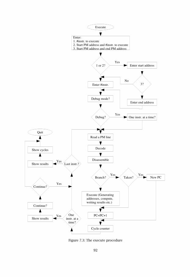
Figure 7.3: The execute procedure
�
Execute
Enter:1. #instr. to execute2. Start PM address and #instr. to execute3. Start PM address and end PM address
1 or 2?
Enter #instr.
YesEnter start address
3?
Enter end address
No
Debug mode?
Debug?Yes
One instr. at a time?
Read a PM line
Decode
Disassemble
Branch?Yes
New PC
Execute (Generating addresses, compute, writing results etc.)
Taken?
PC=PC+1
Yes
Cycle counter
One instr. at a time?
Show resultsYes
Continue?
Continue?
Last instr.?Show resultsYes
Yes
Show cycles
Quit
7.6 Results
When designing the simulator it was discovered that some of the designsteps was hard to implement and some could not be implemented at all.This forced us to redesign the instruction set many times. It might havebeen better to start designing the simulator earlier in the project instead ofin the end in order to find the design mistakes at an earlier stage.
Only MOVE, SIMD and P_FLOW was implemented in the simulator. This wasbecause of the time limit of this project. However, it might have been betterto implement some other instruction types instead because the SIMD modeis designed for accelerating of media applications and is not so useful forsome of the standard algorithms that the competitors use forbenchmarking. In this way, it's quite hard to compare this DSP processor tothe competition. In those cases that we were able to benchmark thisprocessor in the same way as the others the performance was impressive.More about the benchmarks is in chapter 8.
�

�
8Benchmarking
8.1 Preview
Benchmarking is used for revealing strength and weakness of the processorsin certain applications. And now, when the instruction set simulator is readyto use, we can check our processor architecture and the instruction set forreaching the specification requirements. The only way of checking is to writesome special programs (assembly code) for this processor. As a result ofpassing this program through the ISS, the number of expended clock cyclesare counted.
8.2 Benchmarking Strategy
The designed MDSP processor was aimed at media data processing. Themost popular and often used media algorithms are JPEG, MPEG and MP3.According to the designed processor architecture we have SIMD data paths,and single MAC data paths. In order to speed up the benchmark processing,the Dual MAC mode is also used.
The SIMD data paths should be used for eight-by-eight bit multiplicationloops algorithms, for calculating vector DOT multiplication product (motioncompensation stage of a MPEG) or for calculating “sum of absolutedifferences” product (motion estimation stage).
DMAC hardware is used for those algorithms that use the sixteen-by-sixteen bit multiplication loops.
�
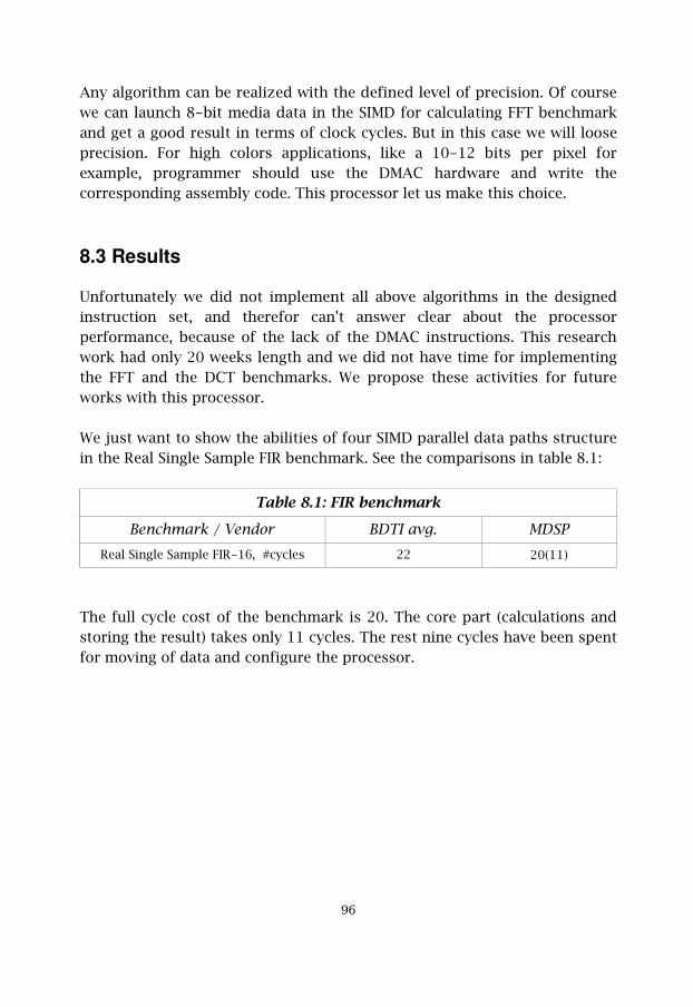
Any algorithm can be realized with the defined level of precision. Of coursewe can launch 8-bit media data in the SIMD for calculating FFT benchmarkand get a good result in terms of clock cycles. But in this case we will looseprecision. For high colors applications, like a 10-12 bits per pixel forexample, programmer should use the DMAC hardware and write thecorresponding assembly code. This processor let us make this choice.
8.3 Results
Unfortunately we did not implement all above algorithms in the designedinstruction set, and therefor can't answer clear about the processorperformance, because of the lack of the DMAC instructions. This researchwork had only 20 weeks length and we did not have time for implementingthe FFT and the DCT benchmarks. We propose these activities for futureworks with this processor.
We just want to show the abilities of four SIMD parallel data paths structurein the Real Single Sample FIR benchmark. See the comparisons in table 8.1:
Table 8.1: FIR benchmark
Benchmark / Vendor BDTI avg. MDSPReal Single Sample FIR-16, #cycles 22 20(11)
The full cycle cost of the benchmark is 20. The core part (calculations andstoring the result) takes only 11 cycles. The rest nine cycles have been spentfor moving of data and configure the processor.
�
9Conclusions
This chapter presents the results and the conclusions from the project andsummarizes all designers ideas for future changes and improvements.
9.1 Results
From the beginning of this final year project we aimed for designing a highperformance DSP with accelerated media functions. We soon realized thatthis was impossible with the limited time that was offered. We decided tofocus on the SIMD part of the design and all our results are based on this.
In fact, we have designed the processor's core according to a givenspecification. We have researched the possibility's for hardware acceleratingof media DSP applications. The complete instruction set for the designedprocessor is presented in this work (except interrupts handling). Theinstruction set simulator was designed only for SIMD parallel computationalpaths of the processor. We have stopped at the benchmarking design stepdue to lack of time and have not completely verified our architecture andinstruction set. That is why we can't release the performance results and canonly expect them according to our research efforts.
The designed processor should show good performance for 8/16-bitconvolution based algorithms. The motion estimation and compensation(MPEG) applications should also be solved very well because of thearchitectural improvements made especially for them. The designedaddressing models gives the opportunity to process the multidimensionalmedia algorithms with a high-level of flexibility of the data accesses.
�
The high level of orthogonality of the instruction set and the architecturegives the designers the possibility of using all available (6!!!) data pathssimultaneously. In this way, six different results are calculated at the sametime, four loop results to the memories, and two auxiliary registeroperations.
The SIMD parallel data paths can process 8-bit media data with a greatperformance for non high-quality color applications, up to five significantbits per pixel. To process data with high-quality colors, programmersshould use the DMAC mode.
In addition, the sophisticated ALU unit offers the possibility to speed up theexecution of logic, arithmetic, and shift operations.
The designed instruction set is quite flexible for future improvements andchanges.
9.2 Future work and improvements
All incomplete issues and activities for this processor should be finished inorder to release the core. Completing the architecture and implementing itin RTL code with a following verification.
In the SIMD part, the memory accessing could be changed for a more flexibleway to address data. In our design, when working with 8-bit data, we storetwo operands in each memory line. However this is not good for someapplications where we have to multiply the data with coefficients as in FFT,FIR for example. It would be better if we could access two 8-bit operandsfrom different memories instead. In this case we could use two memoriesthat contains the data and the other two can contain the coefficients. If thisis done and we use modulo addressing on the coefficient memories, thenthe performance of coefficient based applications can be greatly improved.
In our research we did not pay attention on the interrupts handling.Interrupts of course are necessary for proper processor's exploitation. Thedirect memory access (DMA) unit could significantly improve the totalprocessor performance due to data memory accesses are always thebottleneck.
�
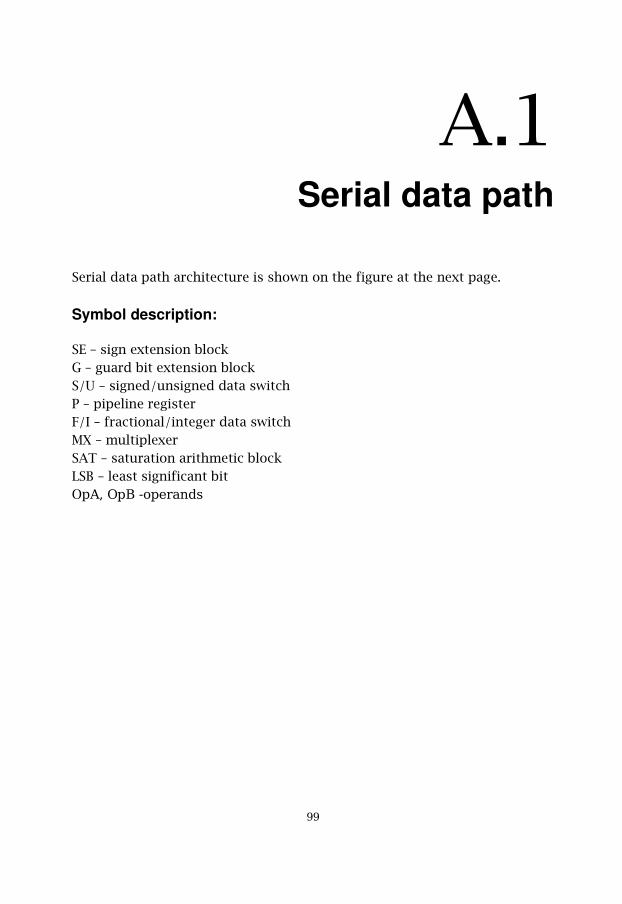
A.1Serial data path
Serial data path architecture is shown on the figure at the next page.
Symbol description:
SE – sign extension blockG – guard bit extension blockS/U – signed/unsigned data switchP – pipeline registerF/I – fractional/integer data switchMX – multiplexerSAT – saturation arithmetic blockLSB – least significant bitOp�>�4�"�?��������
�((
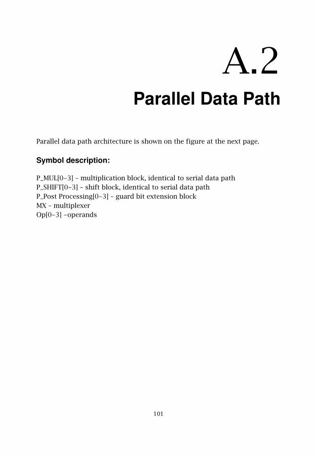
A.2Parallel Data Path
Parallel data path architecture is shown on the figure at the next page.�
Symbol description:
P_MUL[0-3] – multiplication block, identical to serial data pathP_SHIFT[0-3] – shift block, identical to serial data pathP_Post Processing[0-3] – guard bit extension blockMX – multiplexerOp[0-3] -operands
�(�
�(�

B.1A guide to the instruction set
�(�
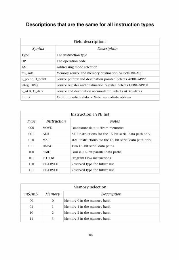
Descriptions that are the same for all instruction types
Field descriptions
Syntax DescriptionType The instruction type
OP The operation code
AM Addressing mode selection
mS, mD Memory source and memory destination. Selects M0-M3
S_point, D_point Source pointer and destination pointer. Selects APR0-APR7
SReg, DReg Source register and destination register. Selects GPR0-GPR31
S_ACR, D_ACR Source and destination accumulator. Selects ACR0-ACR7
ImmX X-bit immediate data or X-bit immediate address
Instruction TYPE list
Type Instruction Notes000 MOVE Load/store data to/from memories
001 ALU ALU instructions for the 16-bit serial data path only
010 MAC MAC instructions for the 16-bit serial data path only
011 DMAC Two 16-bit serial data paths
100 SIMD Four 8-16-bit parallel data paths
101 P_FLOW Program Flow instructions
110 RESERVED Reserved type for future use
111 RESERVED Reserved type for future use
Memory selection
mS/mD Memory Description00 0 Memory 0 in the memory bank
01 1 Memory 1 in the memory bank
10 2 Memory 2 in the memory bank
11 3 Memory 3 in the memory bank
�(�
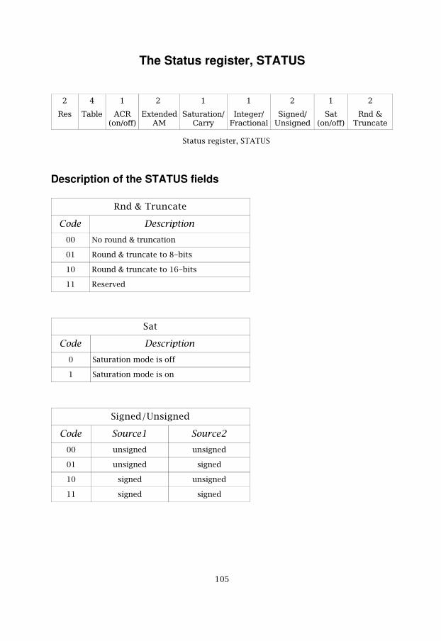
The Status register, STATUS
�
$��
�
%� ��
�
�+$,��-���.
��
/0�������1
�
���������-+����
�
�������-2�� ������
�
�����-3�������
�
��,��-���.
�
$���!%��� ���
Status register, STATUS
Description of the STATUS fields
Rnd & Truncate
Code Description00 No round & truncation
01 Round & truncate to 8-bits
10 Round & truncate to 16-bits
11 Reserved
Sat
Code Description0 Saturation mode is off
1 Saturation mode is on
Signed/Unsigned
Code Source1 Source200 unsigned unsigned
01 unsigned signed
10 signed unsigned
11 signed signed
�(�
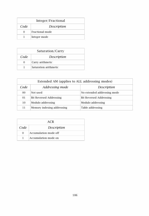
Integer/Fractional
Code Description0 Fractional mode
1 Integer mode
Saturation/Carry
Code Description0 Carry arithmetic
1 Saturation arithmetic
Extended AM (applies to ALL addressing modes)
Code Addressing mode Description00 Not used No extended addressing mode
01 Bit Reversed Addressing Bit Reversed Addressing
10 Modulo addressing Modulo addressing
11 Memory indexing addressing Table addressing
ACR
Code Description0 Accumulation mode off
1 Accumulation mode on
�(�
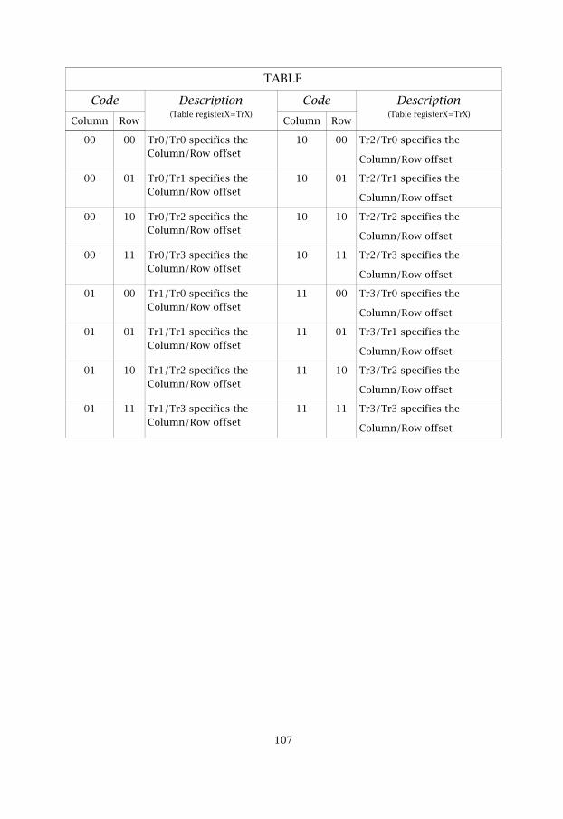
TABLE
CodeColumn Row
Description(Table registerX=TrX)
CodeColumn Row
Description(Table registerX=TrX)
00 00 Tr0/Tr0 specifies theColumn/Row offset
10 00 Tr2/Tr0 specifies the
Column/Row offset
00 01 Tr0/Tr1 specifies theColumn/Row offset
10 01 Tr2/Tr1 specifies the
Column/Row offset
00 10 Tr0/Tr2 specifies theColumn/Row offset
10 10 Tr2/Tr2 specifies the
Column/Row offset
00 11 Tr0/Tr3 specifies theColumn/Row offset
10 11 Tr2/Tr3 specifies the
Column/Row offset
01 00 Tr1/Tr0 specifies theColumn/Row offset
11 00 Tr3/Tr0 specifies the
Column/Row offset
01 01 Tr1/Tr1 specifies theColumn/Row offset
11 01 Tr3/Tr1 specifies the
Column/Row offset
01 10 Tr1/Tr2 specifies theColumn/Row offset
11 10 Tr3/Tr2 specifies the
Column/Row offset
01 11 Tr1/Tr3 specifies theColumn/Row offset
11 11 Tr3/Tr3 specifies the
Column/Row offset
�(�
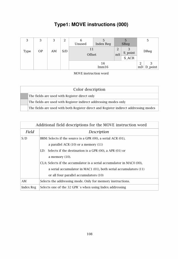
Type1: MOVE instructions (000)
�
%���
�
45
�
�1
�
-6
�3������
�����0�$���
�$��
��
4�����
�
�
�7�����
7�+$
�
6$��
�������
��6
�67�����
MOVE instruction word
Color descriptionThe fields are used with Register direct only
The fields are used with Register indirect addressing modes only
The fields are used with both Register direct and Register indirect addressing modes
Additional field descriptions for the MOVE instruction word
Field DescriptionS/D BRM: Selects if the source is a GPR (00), a serial ACR (01),
a parallel ACR (10) or a memory (11)
LD: Selects if the destination is a GPR (00), a APR (01) or
a memory (10).
CLA: Selects if the accumulator is a serial accumulator in MAC0 (00),
a serial accumulator in MAC1 (01), both serial accumulators (11)
or all four parallel accumulators (10)
AM Selects the addressing mode. Only for memory instructions.
Index Reg Selects one of the 32 GPR`s when using Index addressing
�(�
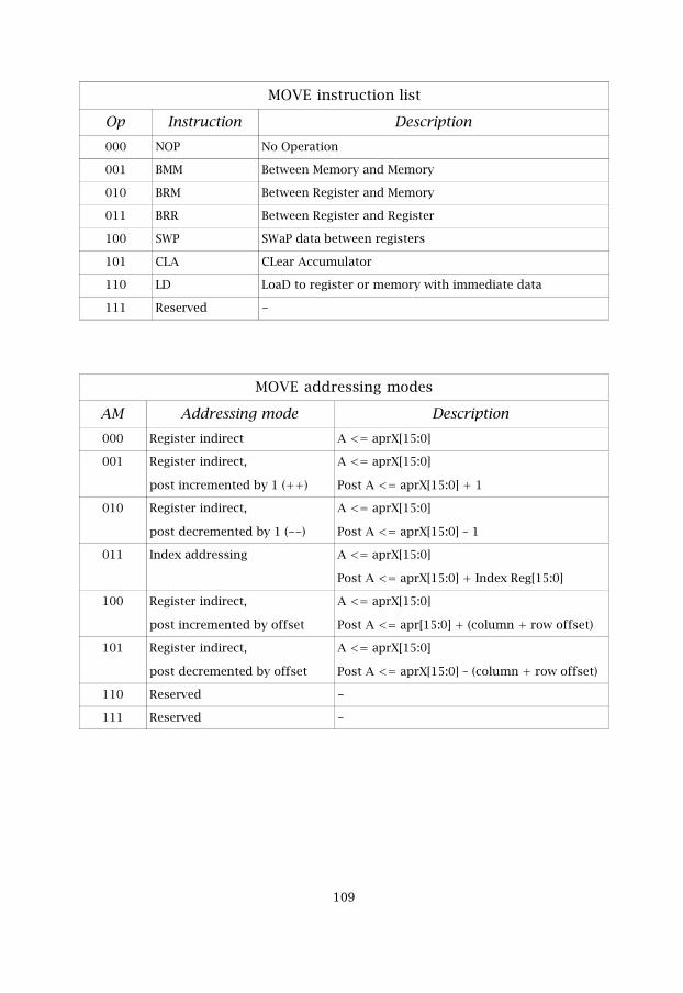
MOVE instruction list
Op Instruction Description000 NOP No Operation
001 BMM Between Memory and Memory
010 BRM Between Register and Memory
011 BRR Between Register and Register
100 SWP SWaP data between registers
101 CLA CLear Accumulator
110 LD LoaD to register or memory with immediate data
111 Reserved -
MOVE addressing modes
AM Addressing mode Description000 Register indirect A <= aprX[15:0]
001 Register indirect,
post incremented by 1 (++)
A <= aprX[15:0]
Post A <= aprX[15:0] + 1
010 Register indirect,
post decremented by 1 (--)
A <= aprX[15:0]
Post A <= aprX[15:0] – 1
011 Index addressing A <= aprX[15:0]
Post A <= aprX[15:0] + Index Reg[15:0]
100 Register indirect,
post incremented by offset
A <= aprX[15:0]
Post A <= apr[15:0] + (column + row offset)
101 Register indirect,
post decremented by offset
A <= aprX[15:0]
Post A <= aprX[15:0] – (column + row offset)
110 Reserved -
111 Reserved -
�(
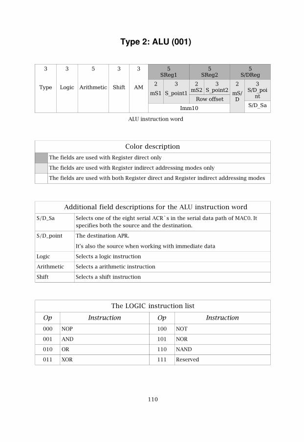
Type 2: ALU (001)
�
%���
�
&���
�
���������
�
����
�
�1
�$���
�$���
�-6$��
�
��
�
7������
���
�7������
$�8�������
����(
�
�-6
�-67���
��
-67�
ALU instruction word
Color descriptionThe fields are used with Register direct only
The fields are used with Register indirect addressing modes only
The fields are used with both Register direct and Register indirect addressing modes
Additional field descriptions for the ALU instruction wordS/D_Sa Selects one of the eight serial ACR`s in the serial data path of MAC0. It
specifies both the source and the destination.
S/D_point The destination APR.
It's also the source when working with immediate data
Logic Selects a logic instruction
Arithmetic Selects a arithmetic instruction
Shift Selects a shift instruction
The LOGIC instruction list
Op Instruction Op Instruction000 NOP 100 NOT
001 AND 101 NOR
010 OR 110 NAND
011 XOR 111 Reserved
��(
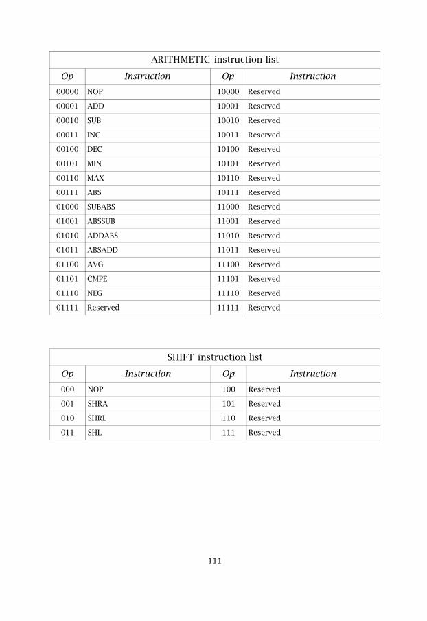
ARITHMETIC instruction list
Op Instruction Op Instruction00000 NOP 10000 Reserved
00001 ADD 10001 Reserved
00010 SUB 10010 Reserved
00011 INC 10011 Reserved
00100 DEC 10100 Reserved
00101 MIN 10101 Reserved
00110 MAX 10110 Reserved
00111 ABS 10111 Reserved
01000 SUBABS 11000 Reserved
01001 ABSSUB 11001 Reserved
01010 ADDABS 11010 Reserved
01011 ABSADD 11011 Reserved
01100 AVG 11100 Reserved
01101 CMPE 11101 Reserved
01110 NEG 11110 Reserved
01111 Reserved 11111 Reserved
SHIFT instruction list
Op Instruction Op Instruction000 NOP 100 Reserved
001 SHRA 101 Reserved
010 SHRL 110 Reserved
011 SHL 111 Reserved
���
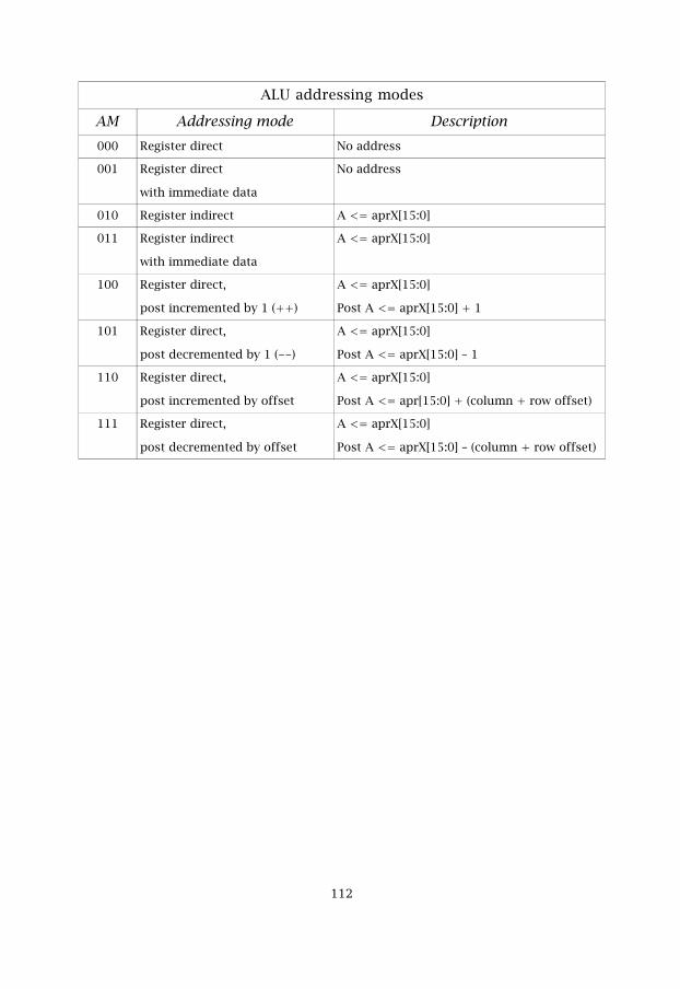
ALU addressing modes
AM Addressing mode Description000 Register direct No address
001 Register direct
with immediate data
No address
010 Register indirect A <= aprX[15:0]
011 Register indirect
with immediate data
A <= aprX[15:0]
100 Register direct,
post incremented by 1 (++)
A <= aprX[15:0]
Post A <= aprX[15:0] + 1
101 Register direct,
post decremented by 1 (--)
A <= aprX[15:0]
Post A <= aprX[15:0] – 1
110 Register direct,
post incremented by offset
A <= aprX[15:0]
Post A <= apr[15:0] + (column + row offset)
111 Register direct,
post decremented by offset
A <= aprX[15:0]
Post A <= aprX[15:0] – (column + row offset)
���
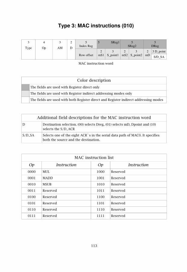
Type 3: MAC instructions (010)
3
Type
4
Op
3
AM
2
D
5Index Reg
5 SReg1 5SReg2
5DReg
Row offset
2mS1
3S_point1
2mS2
3S_point2
2mD
3 D_point
S/D_SA
MAC instruction word
Color descriptionThe fields are used with Register direct only
The fields are used with Register indirect addressing modes only
The fields are used with both Register direct and Register indirect addressing modes
Additional field descriptions for the MAC instruction wordD Destination selection. (00) selects Dreg, (01) selects mD, Dpoint and (10)
selects the S/D_ACR
S/D_SA Selects one of the eight ACR`s in the serial data path of MAC0. It specifiesboth the source and the destination.
MAC instruction list
Op Instruction Op Instruction0000 MUL 1000 Reserved
0001 MADD 1001 Reserved
0010 MSUB 1010 Reserved
0011 Reserved 1011 Reserved
0100 Reserved 1100 Reserved
0101 Reserved 1101 Reserved
0110 Reserved 1110 Reserved
0111 Reserved 1111 Reserved
���
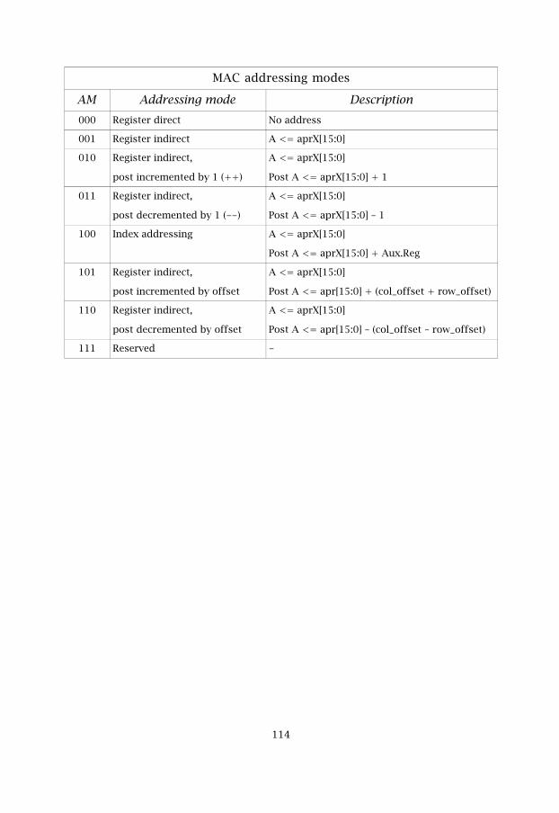
MAC addressing modes
AM Addressing mode Description000 Register direct No address
001 Register indirect A <= aprX[15:0]
010 Register indirect,
post incremented by 1 (++)
A <= aprX[15:0]
Post A <= aprX[15:0] + 1
011 Register indirect,
post decremented by 1 (--)
A <= aprX[15:0]
Post A <= aprX[15:0] – 1
100 Index addressing A <= aprX[15:0]
Post A <= aprX[15:0] + Aux.Reg
101 Register indirect,
post incremented by offset
A <= aprX[15:0]
Post A <= apr[15:0] + (col_offset + row_offset)
110 Register indirect,
post decremented by offset
A <= aprX[15:0]
Post A <= apr[15:0] – (col_offset – row_offset)
111 Reserved -
���
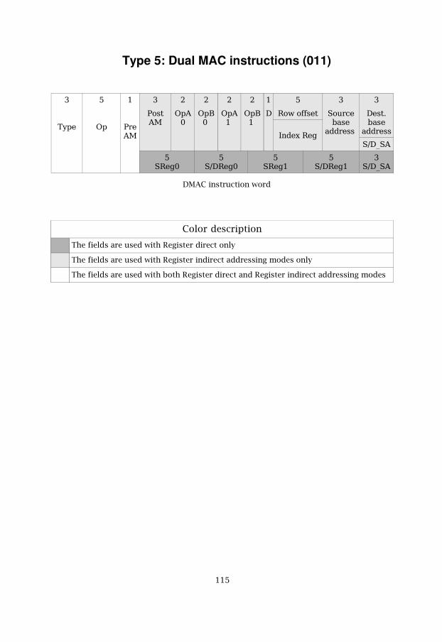
Type 5: Dual MAC instructions (011)
�
%���
�
4�
�
5���1
�������
5����1
�
4��(
�
4�"(�
�
4����
�
4�"��
�
6
�
$�8�������
�����0�$��
�
��� � ���
��������
�
6���) ���
�������
-67�
�$��(
�-6$��(
�$���
�-6$���
�-67�
DMAC instruction word
Color descriptionThe fields are used with Register direct only
The fields are used with Register indirect addressing modes only
The fields are used with both Register direct and Register indirect addressing modes
���

Additional field descriptions for the DMAC instruction wordPre AM Selects if addressing mode is Register indirect (0) or Register direct (1)
Post AM Selects the post changes for Register indirect
OpA0 Selects one of the four memories thatgives Operand A for MAC0
OpB0 Selects one of the four memories thatgives Operand B for MAC0
OpA1 Selects one of the four memories thatgives Operand A for MAC1
OpB1 Selects one of the four memories thatgives Operand B for MAC1
OpXY selects one of the four memoriesand together with the base address, thatis the same for all memories, fouroperands are given. The operands aretaken from four different memories.
D Selects if the destination is a memory (0) or an accumulator register (1) whenusing Register indirect
S/D_SA Selects one of the eight serial ACR`s (SA`s) that is both the source anddestination when ACR is turned on in the status register, STATUS
SReg0 Selects one of the 32 GPR`s that is the source 1 for MAC0
S/DReg0 Selects one of the 32 GPR`s that is the source 2 for MAC0.
When implied addressing is used, this is also the destination
SReg1 Selects one of the 32 GPR`s that is the source 1 for MAC1
S/DReg1 Selects one of the 32 GPR`s that is the source 2 for MAC1.
When implied addressing is used, this is also the destination
���
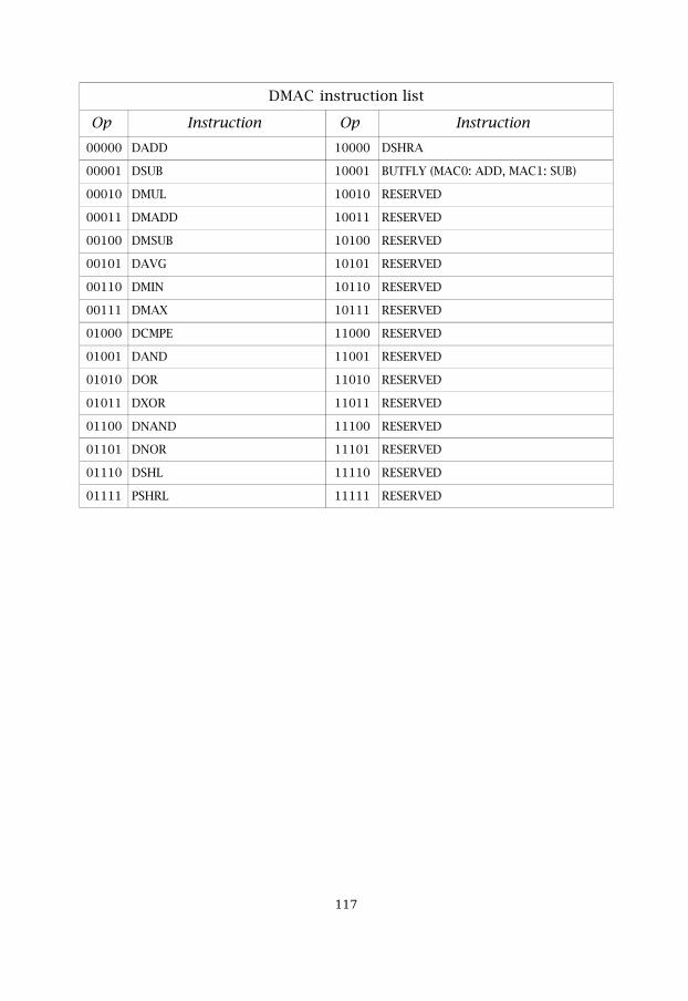
DMAC instruction list
Op Instruction Op Instruction 00000 DADD 10000 DSHRA
00001 DSUB 10001 BUTFLY (MAC0: ADD, MAC1: SUB)
00010 DMUL 10010 RESERVED
00011 DMADD 10011 RESERVED
00100 DMSUB 10100 RESERVED
00101 DAVG 10101 RESERVED
00110 DMIN 10110 RESERVED
00111 DMAX 10111 RESERVED
01000 DCMPE 11000 RESERVED
01001 DAND 11001 RESERVED
01010 DOR 11010 RESERVED
01011 DXOR 11011 RESERVED
01100 DNAND 11100 RESERVED
01101 DNOR 11101 RESERVED
01110 DSHL 11110 RESERVED
01111 PSHRL 11111 RESERVED
���
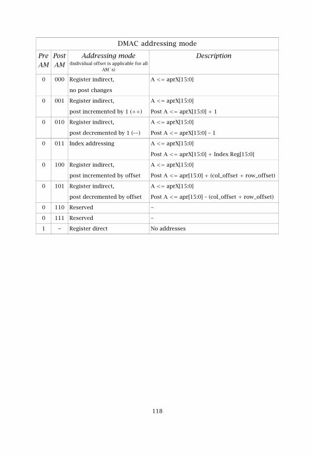
DMAC addressing mode
PreAM
PostAM
Addressing mode(Individual offset is applicable for all
AM`s)
Description
0 000 Register indirect,
no post changes
A <= aprX[15:0]
0 001 Register indirect,
post incremented by 1 (++)
A <= aprX[15:0]
Post A <= aprX[15:0] + 1
0 010 Register indirect,
post decremented by 1 (––)
A <= aprX[15:0]
Post A <= aprX[15:0] – 1
0 011 Index addressing A <= aprX[15:0]
Post A <= aprX[15:0] + Index Reg[15:0]
0 100 Register indirect,
post incremented by offset
A <= aprX[15:0]
Post A <= apr[15:0] + (col_offset + row_offset)
0 101 Register indirect,
post decremented by offset
A <= aprX[15:0]
Post A <= apr[15:0] – (col_offset + row_offset)
0 110 Reserved -
0 111 Reserved -
1 - Register direct No addresses
���
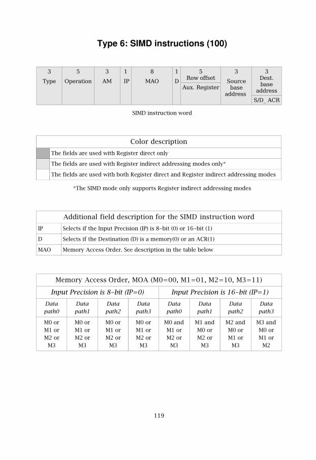
Type 6: SIMD instructions (100)
�
%���
�
4��������
�
�1
�
��5
�
1�4
�
6
�$�8�������
��0)�$�������
�
��� � ���
��������
�6���) ���
�������
-67��+$
SIMD instruction word
Color descriptionThe fields are used with Register direct only
The fields are used with Register indirect addressing modes only*
The fields are used with both Register direct and Register indirect addressing modes
*The SIMD mode only supports Register indirect addressing modes
Additional field description for the SIMD instruction wordIP Selects if the Input Precision (IP) is 8-bit (0) or 16-bit (1)
D Selects if the Destination (D) is a memory(0) or an ACR(1)
MAO Memory Access Order. See description in the table below
Memory Access Order, MOA (M0=00, M1=01, M2=10, M3=11)
Input Precision is 8-bit (IP=0) Input Precision is 16-bit (IP=1)Datapath0
Datapath1
Datapath2
Datapath3
Datapath0
Datapath1
Datapath2
Datapath3
M0 orM1 orM2 or
M3
M0 orM1 orM2 or
M3
M0 orM1 orM2 or
M3
M0 orM1 orM2 or
M3
M0 andM1 orM2 or
M3
M1 andM0 orM2 or
M3
M2 andM0 orM1 or
M3
M3 andM0 orM1 or
M2
��
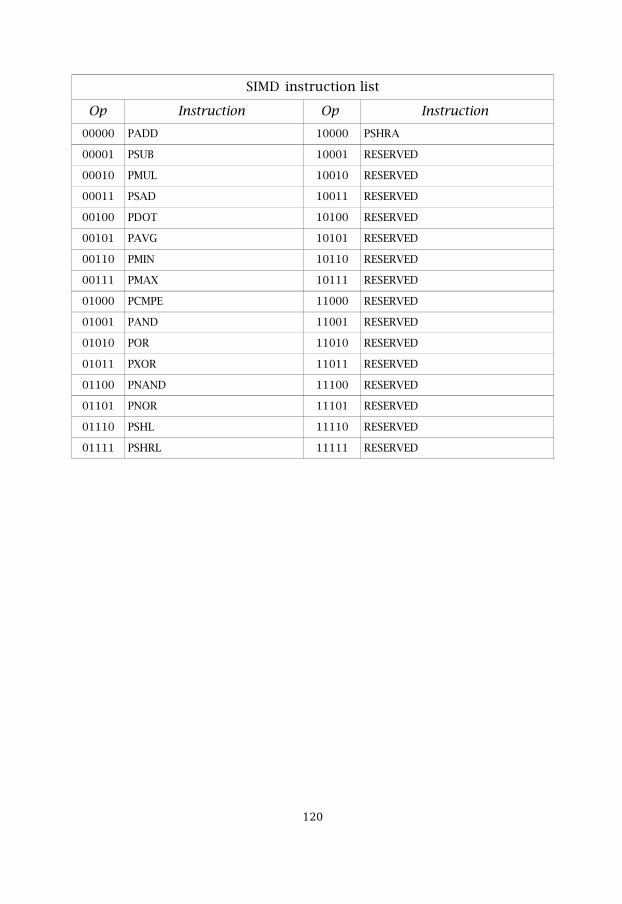
SIMD instruction list
Op Instruction Op Instruction 00000 PADD 10000 PSHRA
00001 PSUB 10001 RESERVED
00010 PMUL 10010 RESERVED
00011 PSAD 10011 RESERVED
00100 PDOT 10100 RESERVED
00101 PAVG 10101 RESERVED
00110 PMIN 10110 RESERVED
00111 PMAX 10111 RESERVED
01000 PCMPE 11000 RESERVED
01001 PAND 11001 RESERVED
01010 POR 11010 RESERVED
01011 PXOR 11011 RESERVED
01100 PNAND 11100 RESERVED
01101 PNOR 11101 RESERVED
01110 PSHL 11110 RESERVED
01111 PSHRL 11111 RESERVED
��(
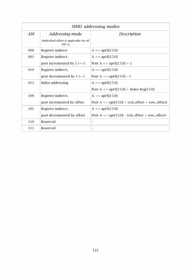
SIMD addressing modes
AM Addressing mode(Individual offset is applicable for all
AM`s)
Description
000 Register indirect A <= aprX[15:0]
001 Register indirect,
post incremented by 1 (++)
A <= aprX[15:0]
Post A <= aprX[15:0] + 1
010 Register indirect,
post decremented by 1 (--)
A <= aprX[15:0]
Post A <= aprX[15:0] – 1
011 Index addressing A <= aprX[15:0]
Post A <= aprX[15:0] + Index Reg[15:0]
100 Register indirect,
post incremented by offset
A <= aprX[15:0]
Post A <= apr[15:0] + (col_offset + row_offset)
101 Register indirect,
post decremented by offset
A <= aprX[15:0]
Post A <= apr[15:0] – (col_offset + row_offset)
110 Reserved -
111 Reserved -
���
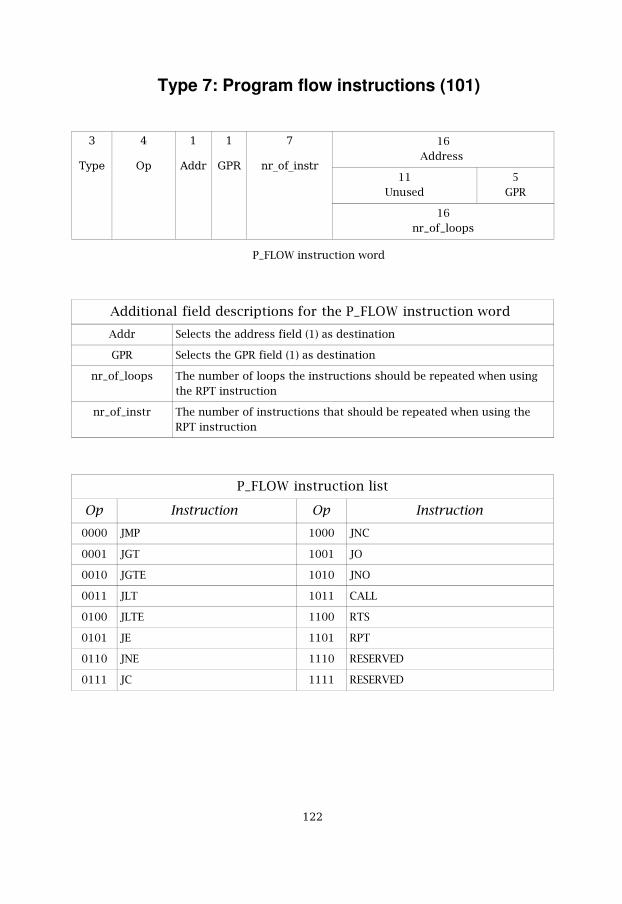
Type 7: Program flow instructions (101)
�
%���
�
4�
�
����
�
95$
�
��7��7�����
16Address
11Unused
5GPR
16nr_of_loops
P_FLOW instruction word
Additional field descriptions for the P_FLOW instruction word
Addr Selects the address field (1) as destination
GPR Selects the GPR field (1) as destination
nr_of_loops The number of loops the instructions should be repeated when usingthe RPT instruction
nr_of_instr The number of instructions that should be repeated when using theRPT instruction
P_FLOW instruction list
Op Instruction Op Instruction0000 JMP 1000 JNC
0001 JGT 1001 JO
0010 JGTE 1010 JNO
0011 JLT 1011 CALL
0100 JLTE 1100 RTS
0101 JE 1101 RPT
0110 JNE 1110 RESERVED
0111 JC 1111 RESERVED
���
B.2Instructions Description
This is the full description of all instructions for the processor. There are sixinstruction types in the set. We have collected instructions according totheir alphabetical order. The description includes the following fields:
• Type of instruction – gives the short instruction description andpoints on the instruction functional group.
• Syntax – shows how the assembly code looks like• Operands – what are the data sources• Execution – what the instruction does• Description – flags updating, functional description, any other
comments• Example – execution example
Symbol description
(a|b| ) – a or b or nothing( ) – optional parameter is inside these bracketsm(aprX)_Y – the data pointed by aprX in the memory bank Yh’xxxx’ – hexadecimal data representationb’xxxx’ – binary data representationi/f – integer/fractional data representations/u – signed/unsigned data representationd – register direct addressingdi – register direct with immediate datai - register indirect addressingii – register indirect with immediate datappo/pmo - register indirect plus/minus offset addressing
���

ABS
Type of instruction:ALU instruction. Absolute value, serial data path.
Syntax:abs am, rS1, (rS2), rDabs am, mS1,aprS1, (mS2,aprS2), mD,aprD
Operands: am: d(0),di(1),i(2),ii(3),pinc(4),pdec(5),ppo(6),pmo(7)rS1, rS2, rD: r0 – r31aprS1, aprS2, aprD: apr0 - apr7
Execution:S1 -> abs(S1)
Description:The instruction returns the absolute result from a 16-bit signed operand,the result is placed into the memory, or into the register, selected by theaddressing mode. The flags are updated.
Example:abs pinc, 1,apr3, 0,apr0
Operand Before After
apr3 h’000F’ h’0010’m(apr3)_1 h'FFFE' h'FFFE'm(apr0)_0 h'0000' h'0002'
���
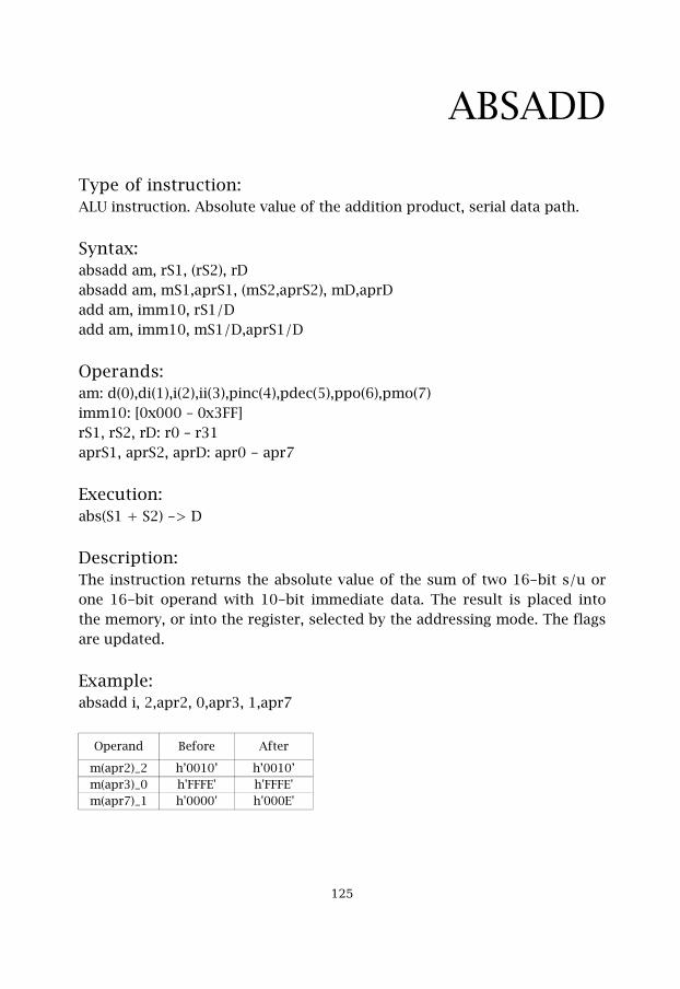
ABSADD
Type of instruction:ALU instruction. Absolute value of the addition product, serial data path.
Syntax:absadd am, rS1, (rS2), rDabsadd am, mS1,aprS1, (mS2,aprS2), mD,aprDadd am, imm10, rS1/Dadd am, imm10, mS1/D,aprS1/D
Operands: am: d(0),di(1),i(2),ii(3),pinc(4),pdec(5),ppo(6),pmo(7)imm10: [0x000 – 0x3FF]rS1, rS2, rD: r0 – r31aprS1, aprS2, aprD: apr0 - apr7
Execution:abs(S1 + S2) -> D
Description:The instruction returns the absolute value of the sum of two 16-bit s/u orone 16-bit operand with 10-bit immediate data. The result is placed intothe memory, or into the register, selected by the addressing mode. The flagsare updated.
Example:absadd i, 2,apr2, 0,apr3, 1,apr7
Operand Before After
m(apr2)_2 h’0010’ h’0010’m(apr3)_0 h'FFFE' h'FFFE'm(apr7)_1 h'0000' h'000E'
���
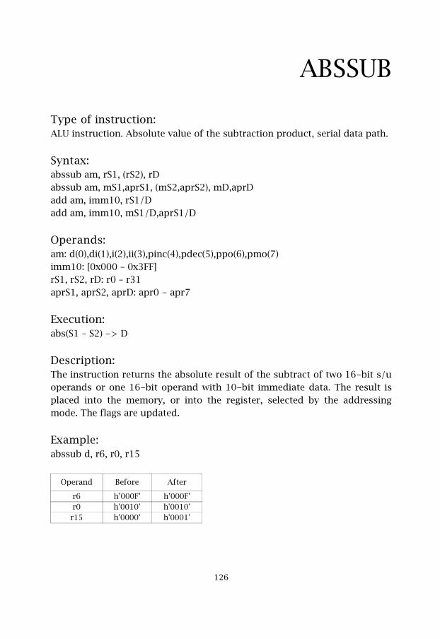
ABSSUB
Type of instruction:ALU instruction. Absolute value of the subtraction product, serial data path.
Syntax:abssub am, rS1, (rS2), rDabssub am, mS1,aprS1, (mS2,aprS2), mD,aprDadd am, imm10, rS1/Dadd am, imm10, mS1/D,aprS1/D
Operands: am: d(0),di(1),i(2),ii(3),pinc(4),pdec(5),ppo(6),pmo(7)imm10: [0x000 – 0x3FF]rS1, rS2, rD: r0 – r31aprS1, aprS2, aprD: apr0 - apr7
Execution:abs(S1 – S2) -> D
Description:The instruction returns the absolute result of the subtract of two 16-bit s/uoperands or one 16-bit operand with 10-bit immediate data. The result isplaced into the memory, or into the register, selected by the addressingmode. The flags are updated.
Example:abssub d, r6, r0, r15
Operand Before After
r6 h’000F’ h’000F’r0 h'0010' h'0010'r15 h'0000' h'0001'
���
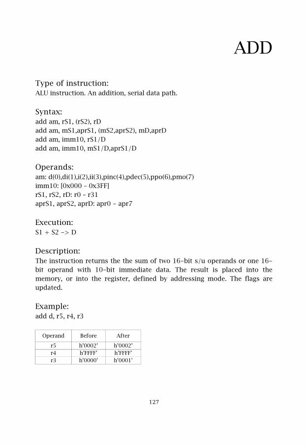
ADD
Type of instruction:ALU instruction. An addition, serial data path.
Syntax:add am, rS1, (rS2), rDadd am, mS1,aprS1, (mS2,aprS2), mD,aprDadd am, imm10, rS1/Dadd am, imm10, mS1/D,aprS1/D
Operands: am: d(0),di(1),i(2),ii(3),pinc(4),pdec(5),ppo(6),pmo(7)imm10: [0x000 – 0x3FF]rS1, rS2, rD: r0 – r31aprS1, aprS2, aprD: apr0 - apr7
Execution:S1 + S2 -> D
Description:The instruction returns the the sum of two 16-bit s/u operands or one 16-bit operand with 10-bit immediate data. The result is placed into thememory, or into the register, defined by addressing mode. The flags areupdated.
Example:add d, r5, r4, r3
Operand Before After
r5 h’0002’ h’0002’r4 h’FFFF’ h’FFFF’r3 h’0000’ h’0001’
���
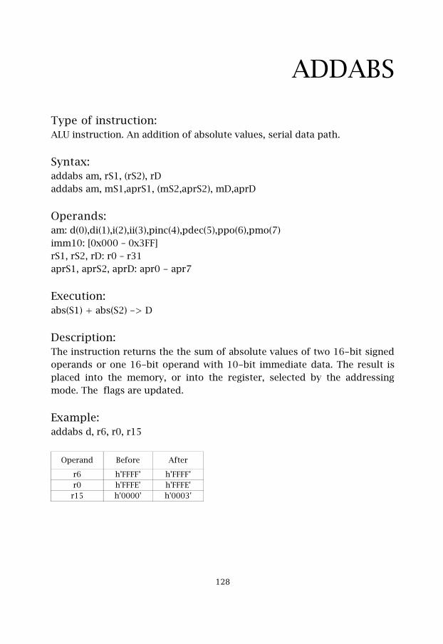
ADDABS
Type of instruction:ALU instruction. An addition of absolute values, serial data path.
Syntax:addabs am, rS1, (rS2), rDaddabs am, mS1,aprS1, (mS2,aprS2), mD,aprD
Operands: am: d(0),di(1),i(2),ii(3),pinc(4),pdec(5),ppo(6),pmo(7)imm10: [0x000 – 0x3FF]rS1, rS2, rD: r0 – r31aprS1, aprS2, aprD: apr0 - apr7
Execution:abs(S1) + abs(S2) -> D
Description:The instruction returns the the sum of absolute values of two 16-bit signedoperands or one 16-bit operand with 10-bit immediate data. The result isplaced into the memory, or into the register, selected by the addressingmode. The flags are updated.
Example:addabs d, r6, r0, r15
Operand Before After
r6 h’FFFF’ h’FFFF’r0 h'FFFE' h'FFFE'r15 h'0000' h'0003'
���
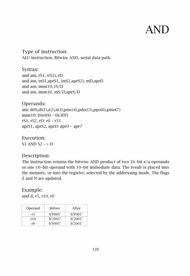
AND
Type of instruction:ALU instruction. Bitwise AND, serial data path.
Syntax:and am, rS1, (rS2), rDand am, mS1,aprS1, (mS2,aprS2), mD,aprDand am, imm10, rS/Dand am, imm10, mS/D,aprS/D
Operands: am: d(0),di(1),i(2),ii(3),pinc(4),pdec(5),ppo(6),pmo(7)imm10: [0x000 – 0x3FF]rS1, rS2, rD: r0 – r31aprS1, aprS2, aprD: apr0 - apr7
Execution:S1 AND S2 -> D
Description:The instruction returns the bitwise AND product of two 16-bit s/u operandsor one 16-bit operand with 10-bit immediate data. The result is placed intothe memory, or into the register, selected by the addressing mode. The flagsZ and N are updated.
Example:and d, r5, r10, r0
Operand Before After
r5 h’F001’ h’F001’r10 h’2001’ h’2001’r0 h’0001’ h’2001’
��
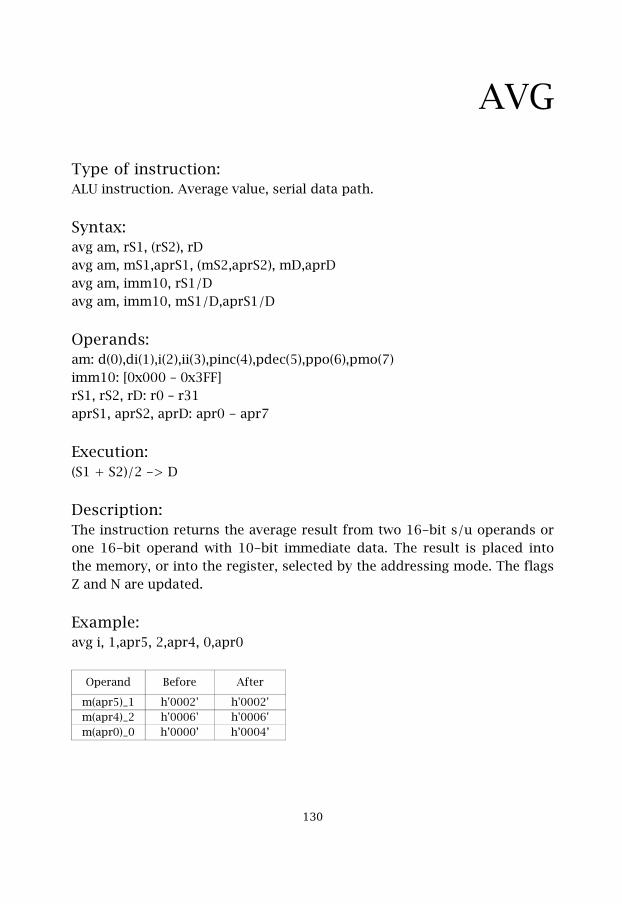
AVG
Type of instruction:ALU instruction. Average value, serial data path.
Syntax:avg am, rS1, (rS2), rDavg am, mS1,aprS1, (mS2,aprS2), mD,aprDavg am, imm10, rS1/Davg am, imm10, mS1/D,aprS1/D
Operands: am: d(0),di(1),i(2),ii(3),pinc(4),pdec(5),ppo(6),pmo(7)imm10: [0x000 – 0x3FF]rS1, rS2, rD: r0 – r31aprS1, aprS2, aprD: apr0 - apr7
Execution:(S1 + S2)/2 -> D
Description:The instruction returns the average result from two 16-bit s/u operands orone 16-bit operand with 10-bit immediate data. The result is placed intothe memory, or into the register, selected by the addressing mode. The flagsZ and N are updated.
Example:avg i, 1,apr5, 2,apr4, 0,apr0
Operand Before After
m(apr5)_1 h'0002' h'0002'm(apr4)_2 h'0006' h'0006'm(apr0)_0 h’0000’ h’0004’
��(
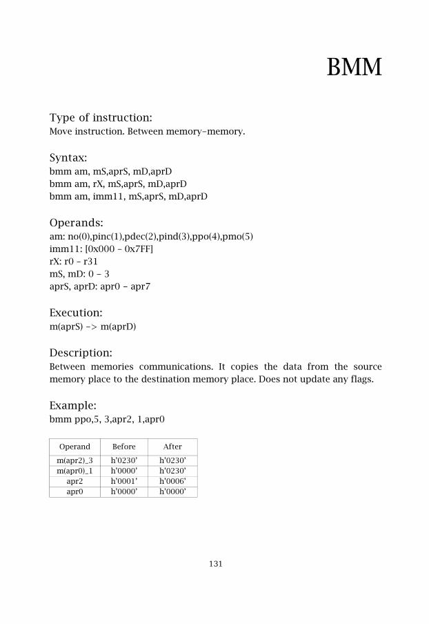
BMM
Type of instruction:Move instruction. Between memory-memory.
Syntax:bmm am, mS,aprS, mD,aprDbmm am, rX, mS,aprS, mD,aprDbmm am, imm11, mS,aprS, mD,aprD
Operands: am: no(0),pinc(1),pdec(2),pind(3),ppo(4),pmo(5)imm11: [0x000 – 0x7FF]rX: r0 – r31mS, mD: 0 - 3aprS, aprD: apr0 - apr7
Execution:m(aprS) -> m(aprD)
Description:Between memories communications. It copies the data from the sourcememory place to the destination memory place. Does not update any flags.
Example:bmm ppo,5, 3,apr2, 1,apr0
Operand Before After
m(apr2)_3 h’0230’ h’0230’m(apr0)_1 h’0000’ h’0230’
apr2 h’0001’ h’0006’apr0 h’0000’ h’0000’
���
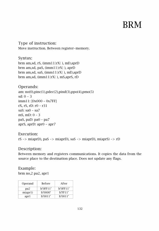
BRM
Type of instruction:Move instruction. Between register-memory.
Syntax:brm am,sd, rS, (imm11|rX| ), mD,aprDbrm am,sd, paS, (imm11|rX| ), aprDbrm am,sd, saS, (imm11|rX| ), mD,aprDbrm am,sd, (imm11|rX| ), mS,aprS, rD
Operands: am: no(0),pinc(1),pdec(2),pind(3),ppo(4),pmo(5)sd: 0 - 3imm11: [0x000 – 0x7FF]rX, rS, rD: r0 – r31saS: sa0 – sa7mS, mD: 0 – 3paS, paD: pa0 – pa7aprS, aprD: apr0 - apr7
Execution:rS -> m(aprD), paS -> m(aprD), saS -> m(aprD), m(aprS) -> rD
Description:Between memory and registers communications. It copies the data from thesource place to the destination place. Does not update any flags.
Example:brm no,2 pa2, apr1
Operand Before After
pa2 h’0FF11’ h’0FF11’m(apr1) h’0000’ h’FF11’
apr1 h’0011’ h’0011’
���
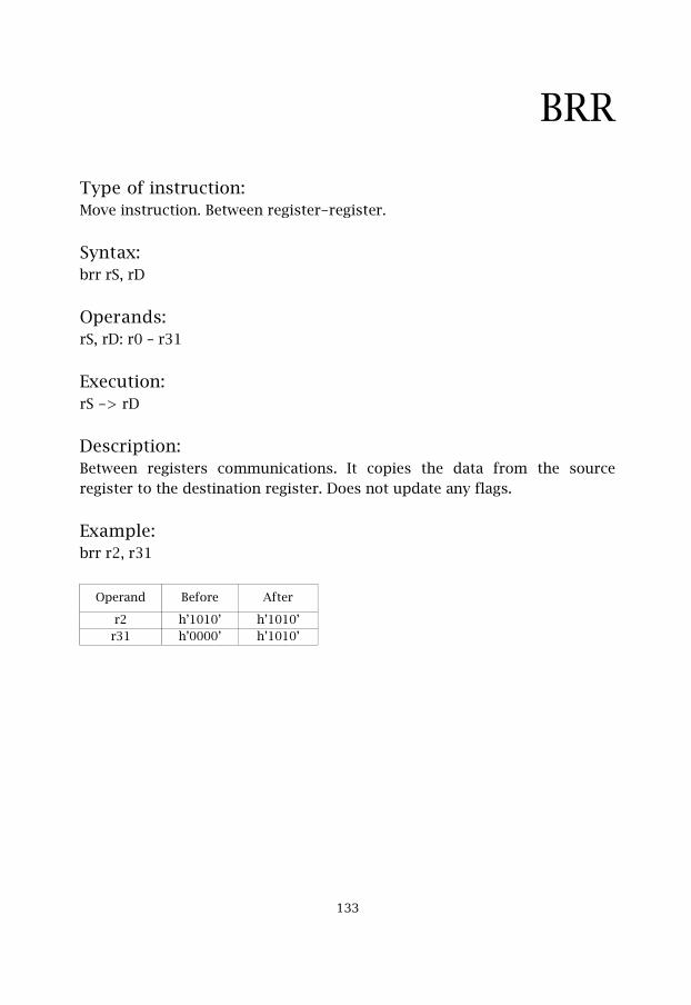
BRR
Type of instruction:Move instruction. Between register-register.
Syntax:brr rS, rD
Operands: rS, rD: r0 – r31
Execution:rS -> rD
Description:Between registers communications. It copies the data from the sourceregister to the destination register. Does not update any flags.
Example:brr r2, r31
Operand Before After
r2 h’1010’ h’1010’r31 h’0000’ h’1010’
���
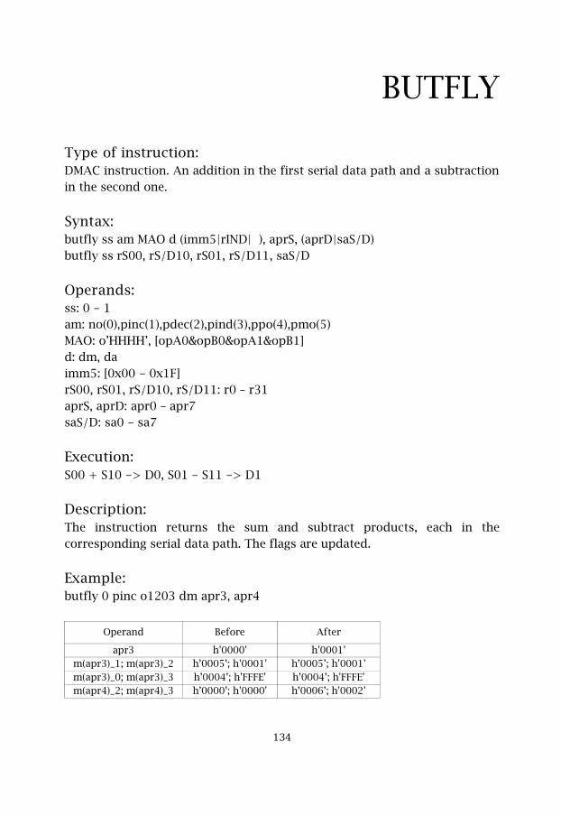
BUTFLY
Type of instruction:DMAC instruction. An addition in the first serial data path and a subtractionin the second one.
Syntax:butfly ss am MAO d (imm5|rIND| ), aprS, (aprD|saS/D)butfly ss rS00, rS/D10, rS01, rS/D11, saS/D
Operands:ss: 0 - 1am: no(0),pinc(1),pdec(2),pind(3),ppo(4),pmo(5)MAO: o’HHHH’, [opA0&opB0&opA1&opB1]d: dm, daimm5: [0x00 - 0x1F]rS00, rS01, rS/D10, rS/D11: r0 – r31aprS, aprD: apr0 – apr7saS/D: sa0 - sa7
Execution:S00 + S10 -> D0, S01 - S11 -> D1
Description:The instruction returns the sum and subtract products, each in thecorresponding serial data path. The flags are updated.
Example:butfly 0 pinc o1203 dm apr3, apr4
Operand Before After
apr3 h'0000' h'0001'm(apr3)_1; m(apr3)_2 h’0005’; h'0001' h’0005’; h'0001'm(apr3)_0; m(apr3)_3 h’0004’; h'FFFE' h’0004’; h'FFFE'm(apr4)_2; m(apr4)_3 h’0000’; h'0000' h’0006’; h'0002'
���
CALL
Type of instruction:P_FLOW instruction. A subroutine call.
Syntax:call dest_address
Operands:dest_address: [0x0000 – 0xFFFF]
Execution:PC <- dest_address
Description:A subroutine call instruction. It provides the absolute unconditional branch.
Example:call sbr3
Operand Before After
PC h’0003’ h’3000’
���
CLA
Type of instruction:Move instruction. Clear the accumulator register.
Syntax:cla sd, paXcla sd, saX
Operands: sd: 0 - 3paX: pa0 – pa7saX: sa0 – sa7
Execution:h’0000’ -> paXh’0000’ -> saX
Description:Clears the accumulator register, that is the serial in MAC0 (0), the serial inMAC1 (1), the parallel ones (2) or the both serials (3), according to sd field.Does not update any flags.
Example:cla 1, sa4
Operand Before After
sd b‘10’ b‘10’sa4 h’023139CD10’ h’0000000000’
���
CMPE
Type of instruction:ALU instruction. Compare to zero, serial data path.
Syntax:cmpe am, rS1, (rS2), rDcmpe am, mS1,aprS1, (mS2,aprS2), mD,aprD
Operands: am: d(0),di(1),i(2),ii(3),pinc(4),pdec(5),ppo(6),pmo(7)rS1, rS2, rD: r0 – r31aprS1, aprS2, aprD: apr0 - apr7
Execution:0 <- if opA != opB , 1 <- if opA = opB
Description:The instruction returns one if two 16-bit s/u operands are equal, and zerootherwise. The result is placed into the memory, or into the register,selected by the addressing mode. The flags O and C are updated.
Example:cmpe d, r6, r3
Operand Before After
r6 h'0002' h'0002'r3 h'0000' h'0000'
���
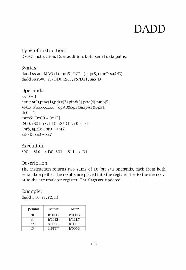
DADD
Type of instruction:DMAC instruction. Dual addition, both serial data paths.
Syntax:dadd ss am MAO d (imm5|rIND| ), aprS, (aprD|saS/D)dadd ss rS00, rS/D10, rS01, rS/D11, saS/D
Operands:ss: 0 - 1am: no(0),pinc(1),pdec(2),pind(3),ppo(4),pmo(5)MAO: b’xxxxxxxx’, [opA0&opB0&opA1&opB1]d: 0 - 1imm5: [0x00 - 0x1F]rS00, rS01, rS/D10, rS/D11: r0 – r31aprS, aprD: apr0 – apr7saS/D: sa0 - sa7
Execution:S00 + S10 -> D0, S01 + S11 -> D1
Description:The instruction returns two sums of 16-bit s/u operands, each from bothserial data paths. The results are placed into the register file, to the memory,or to the accumulator register. The flags are updated.
Example:dadd 1 r0, r1, r2, r3
Operand Before After
r0 h'0006' h'0006'r1 h’11E1’ h’11E7’r2 h’000C’ h’000C’r3 h’FFFF’ h’000B’
���

DAND
Type of instruction:DMAC instruction. Dual bitwise AND, both serial data paths.
Syntax:dand ss am MAO d (imm5|rIND| ), aprS, (aprD|saS/D)dand ss rS00, rS/D10, rS01, rS/D11, saS/D
Operands:ss: 0 - 1am: no(0),pinc(1),pdec(2),pind(3),ppo(4),pmo(5)MAO: b’xxxxxxxx’, [opA0&opB0&opA1&opB1]d: 0 - 1imm5: [0x00 - 0x1F]rS00, rS01, rS/D10, rS/D11: r0 – r31aprS, aprD: apr0 – apr7saS/D: sa0 - sa7
Execution:S00 AND S10 -> D0, S01 AND S11 -> D1
Description:The instruction returns two bitwise AND products between two 16-bit s/uoperands in both serial data paths. The results are placed into the registerfile, to the memory, or to the accumulator. The flags Z and N are updated.
Example:dand 0 pind o0123 da r9, apr3, sa1 (shown for one serial data path)
Operand Before After
apr3 h'0004' b'000D'm(apr3)_0 h’E231’ h’E321’m(apr3)_1 h’DC47’ h’DC47’
sa1_0 h’0000000000’ h’000000C001’
��
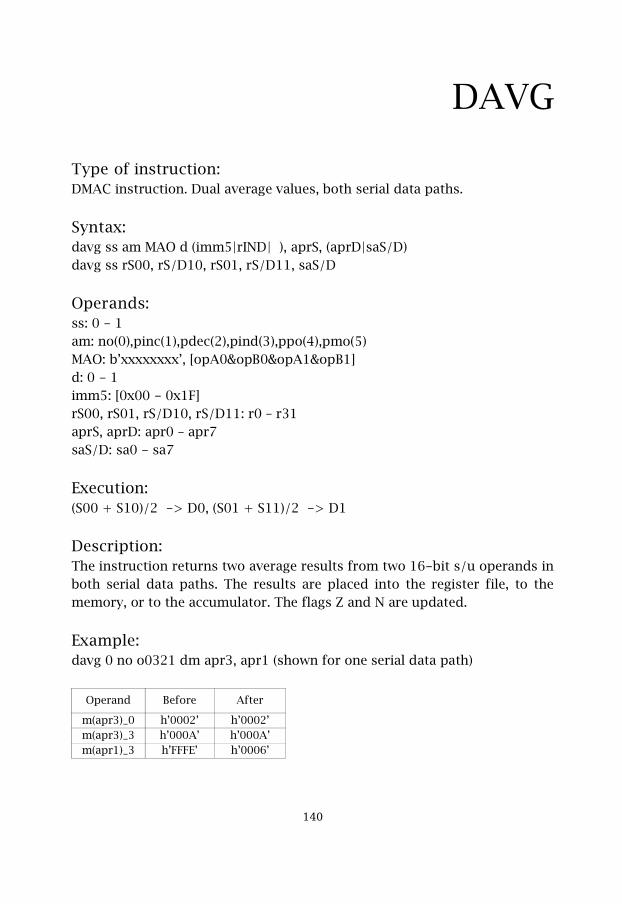
DAVG
Type of instruction:DMAC instruction. Dual average values, both serial data paths.
Syntax:davg ss am MAO d (imm5|rIND| ), aprS, (aprD|saS/D)davg ss rS00, rS/D10, rS01, rS/D11, saS/D
Operands:ss: 0 - 1am: no(0),pinc(1),pdec(2),pind(3),ppo(4),pmo(5)MAO: b’xxxxxxxx’, [opA0&opB0&opA1&opB1]d: 0 - 1imm5: [0x00 - 0x1F]rS00, rS01, rS/D10, rS/D11: r0 – r31aprS, aprD: apr0 – apr7saS/D: sa0 - sa7
Execution:(S00 + S10)/2 -> D0, (S01 + S11)/2 -> D1
Description:The instruction returns two average results from two 16-bit s/u operands inboth serial data paths. The results are placed into the register file, to thememory, or to the accumulator. The flags Z and N are updated.
Example:davg 0 no o0321 dm apr3, apr1 (shown for one serial data path)
Operand Before After
m(apr3)_0 h’0002’ h’0002’m(apr3)_3 h’000A’ h’000A’m(apr1)_3 h’FFFE’ h’0006’
��(
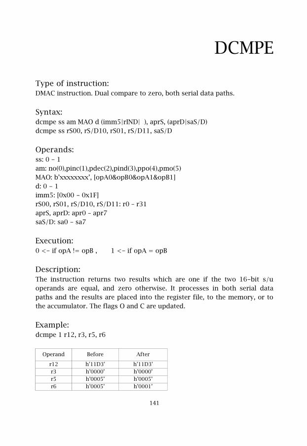
DCMPE
Type of instruction:DMAC instruction. Dual compare to zero, both serial data paths.
Syntax:dcmpe ss am MAO d (imm5|rIND| ), aprS, (aprD|saS/D)dcmpe ss rS00, rS/D10, rS01, rS/D11, saS/D
Operands:ss: 0 - 1am: no(0),pinc(1),pdec(2),pind(3),ppo(4),pmo(5)MAO: b’xxxxxxxx’, [opA0&opB0&opA1&opB1]d: 0 - 1imm5: [0x00 - 0x1F]rS00, rS01, rS/D10, rS/D11: r0 – r31aprS, aprD: apr0 – apr7saS/D: sa0 - sa7
Execution:0 <- if opA != opB , 1 <- if opA = opB
Description:The instruction returns two results which are one if the two 16-bit s/uoperands are equal, and zero otherwise. It processes in both serial datapaths and the results are placed into the register file, to the memory, or tothe accumulator. The flags O and C are updated.
Example:dcmpe 1 r12, r3, r5, r6
Operand Before After
r12 h'11D3' h'11D3'r3 h’0000’ h’0000’r5 h’0005’ h’0005’r6 h’0005’ h’0001’
���

DEC
Type of instruction:ALU instruction. Decrement by 1, serial data path.
Syntax:dec am, rS1, (rS2), rDdec am, mS1,aprS1, (mS2,aprS2), mD,aprD
Operands: am: d(0),di(1),i(2),ii(3),pinc(4),pdec(5),ppo(6),pmo(7)rS1, rS2, rD: r0 – r31aprS1, aprS2, aprD: apr0 - apr7
Execution:S1 - 1 -> D
Description:The instruction returns the decremented by one 16-bit s/u operand. Theresult is placed into the memory, or into the register, defined by addressingmode. The flags are updated.
Example:dec i, 1,apr0, 1,apr1
Operand Before After
m(apr0)_1 h’0020’ h’0020’m(apr1)_1 h’0001’ h’001F’
���
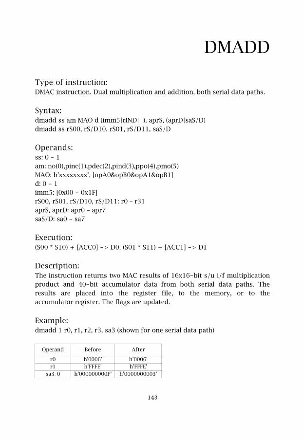
DMADD
Type of instruction:DMAC instruction. Dual multiplication and addition, both serial data paths.
Syntax:dmadd ss am MAO d (imm5|rIND| ), aprS, (aprD|saS/D)dmadd ss rS00, rS/D10, rS01, rS/D11, saS/D
Operands:ss: 0 - 1am: no(0),pinc(1),pdec(2),pind(3),ppo(4),pmo(5)MAO: b’xxxxxxxx’, [opA0&opB0&opA1&opB1]d: 0 - 1imm5: [0x00 - 0x1F]rS00, rS01, rS/D10, rS/D11: r0 – r31aprS, aprD: apr0 – apr7saS/D: sa0 - sa7
Execution:(S00 * S10) + [ACC0] -> D0, (S01 * S11) + [ACC1] -> D1
Description:The instruction returns two MAC results of 16x16-bit s/u i/f multiplicationproduct and 40-bit accumulator data from both serial data paths. Theresults are placed into the register file, to the memory, or to theaccumulator register. The flags are updated.
Example:dmadd 1 r0, r1, r2, r3, sa3 (shown for one serial data path)
Operand Before After
r0 h'0006' h'0006'r1 h’FFFE’ h’FFFE’
sa3_0 h’000000000F’ h’0000000003’
���

DMAX
Type of instruction:DMAC instruction. A maximum values, both serial data paths.
Syntax:dmax ss am MAO d (imm5|rIND| ), aprS, (aprD|saS/D)dmax ss rS00, rS/D10, rS01, rS/D11, saS/D
Operands:ss: 0 - 1am: no(0),pinc(1),pdec(2),pind(3),ppo(4),pmo(5)MAO: b’xxxxxxxx’, [opA0&opB0&opA1&opB1]d: 0 - 1imm5: [0x00 - 0x1F]rS00, rS01, rS/D10, rS/D11: r0 – r31aprS, aprD: apr0 – apr7saS/D: sa0 - sa7
Execution:(S00 - S10) -> D(S10) if D<0, D(S00) if D>=0 (S01 - S11) -> D(S11) if D<0, D(S01) if D>=0
Description:The instruction returns two maximums from two 16-bit s/u operands inboth serial data paths. The results are placed into the register file, to thememory, or to the accumulator. The flags are updated.
Example:dmax 1 r0, r1, r2, r3, sa0 (shown for one serial data path)
Operand Before After
r0 h'FFFF' h'FFFF'r1 h’0002’ h’0002’
sa0_0 h’0000000000’ h’0000000002’
���
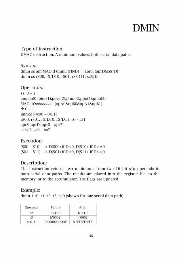
DMIN
Type of instruction:DMAC instruction. A minimum values, both serial data paths.
Syntax:dmin ss am MAO d (imm5|rIND| ), aprS, (aprD|saS/D)dmin ss rS00, rS/D10, rS01, rS/D11, saS/D
Operands:ss: 0 - 1am: no(0),pinc(1),pdec(2),pind(3),ppo(4),pmo(5)MAO: b’xxxxxxxx’, [opA0&opB0&opA1&opB1]d: 0 - 1imm5: [0x00 – 0x1F]rS00, rS01, rS/D10, rS/D11: r0 – r31aprS, aprD: apr0 – apr7saS/D: sa0 - sa7
Execution:(S00 - S10) -> D(S00) if D<0, D(S10) if D>=0 (S01 - S11) -> D(S01) if D<0, D(S11) if D>=0
Description:The instruction returns two minimums from two 16-bit s/u operands inboth serial data paths. The results are placed into the register file, to thememory, or to the accumulator. The flags are updated.
Example:dmin 1 r0, r1, r2, r3, sa0 (shown for one serial data path)
Operand Before After
r2 h'FFFF' h'FFFF'r3 h’0002’ h’0002’
sa0_1 h’0000000000’ h’FFFFFFFFFF’
���
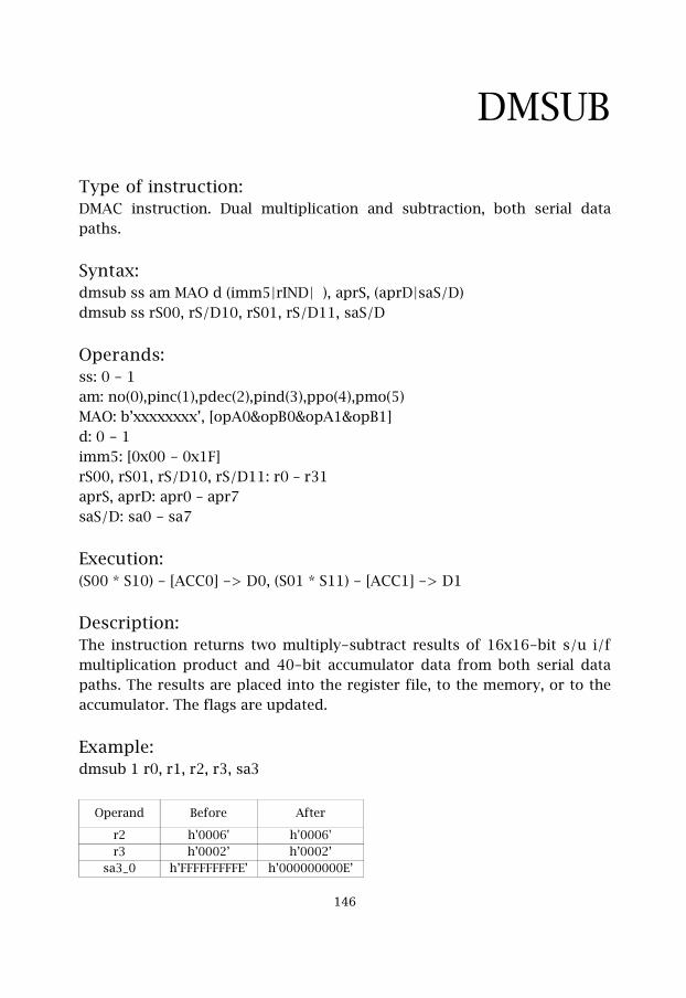
DMSUB
Type of instruction:DMAC instruction. Dual multiplication and subtraction, both serial datapaths.
Syntax:dmsub ss am MAO d (imm5|rIND| ), aprS, (aprD|saS/D)dmsub ss rS00, rS/D10, rS01, rS/D11, saS/D
Operands:ss: 0 - 1am: no(0),pinc(1),pdec(2),pind(3),ppo(4),pmo(5)MAO: b’xxxxxxxx’, [opA0&opB0&opA1&opB1]d: 0 - 1imm5: [0x00 - 0x1F]rS00, rS01, rS/D10, rS/D11: r0 – r31aprS, aprD: apr0 – apr7saS/D: sa0 - sa7
Execution:(S00 * S10) - [ACC0] -> D0, (S01 * S11) - [ACC1] -> D1
Description:The instruction returns two multiply-subtract results of 16x16-bit s/u i/fmultiplication product and 40-bit accumulator data from both serial datapaths. The results are placed into the register file, to the memory, or to theaccumulator. The flags are updated.
Example:dmsub 1 r0, r1, r2, r3, sa3
Operand Before After
r2 h'0006' h'0006'r3 h’0002’ h’0002’
sa3_0 h’FFFFFFFFFE’ h’000000000E’
���
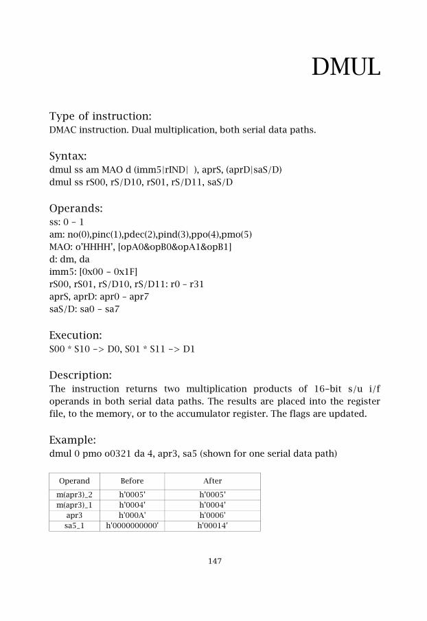
DMUL
Type of instruction:DMAC instruction. Dual multiplication, both serial data paths.
Syntax:dmul ss am MAO d (imm5|rIND| ), aprS, (aprD|saS/D)dmul ss rS00, rS/D10, rS01, rS/D11, saS/D
Operands:ss: 0 - 1am: no(0),pinc(1),pdec(2),pind(3),ppo(4),pmo(5)MAO: o’HHHH’, [opA0&opB0&opA1&opB1]d: dm, daimm5: [0x00 - 0x1F]rS00, rS01, rS/D10, rS/D11: r0 – r31aprS, aprD: apr0 – apr7saS/D: sa0 - sa7
Execution:S00 * S10 -> D0, S01 * S11 -> D1
Description:The instruction returns two multiplication products of 16-bit s/u i/foperands in both serial data paths. The results are placed into the registerfile, to the memory, or to the accumulator register. The flags are updated.
Example:dmul 0 pmo o0321 da 4, apr3, sa5 (shown for one serial data path)
Operand Before After
m(apr3)_2 h’0005’ h’0005’m(apr3)_1 h’0004’ h’0004’
apr3 h'000A' h'0006'sa5_1 h'0000000000' h'00014'
���
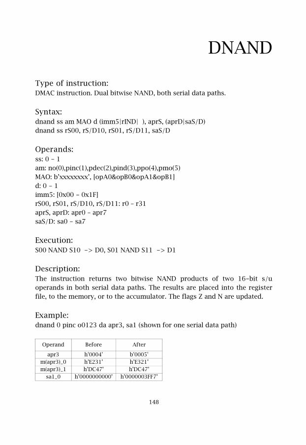
DNAND
Type of instruction:DMAC instruction. Dual bitwise NAND, both serial data paths.
Syntax:dnand ss am MAO d (imm5|rIND| ), aprS, (aprD|saS/D)dnand ss rS00, rS/D10, rS01, rS/D11, saS/D
Operands:ss: 0 - 1am: no(0),pinc(1),pdec(2),pind(3),ppo(4),pmo(5)MAO: b’xxxxxxxx’, [opA0&opB0&opA1&opB1]d: 0 - 1imm5: [0x00 - 0x1F]rS00, rS01, rS/D10, rS/D11: r0 – r31aprS, aprD: apr0 – apr7saS/D: sa0 - sa7
Execution:S00 NAND S10 -> D0, S01 NAND S11 -> D1
Description:The instruction returns two bitwise NAND products of two 16-bit s/uoperands in both serial data paths. The results are placed into the registerfile, to the memory, or to the accumulator. The flags Z and N are updated.
Example:dnand 0 pinc o0123 da apr3, sa1 (shown for one serial data path)
Operand Before After
apr3 h'0004' b'0005'm(apr3)_0 h’E231’ h’E321’m(apr3)_1 h’DC47’ h’DC47’
sa1_0 h’0000000000’ h’0000003FF7’
���
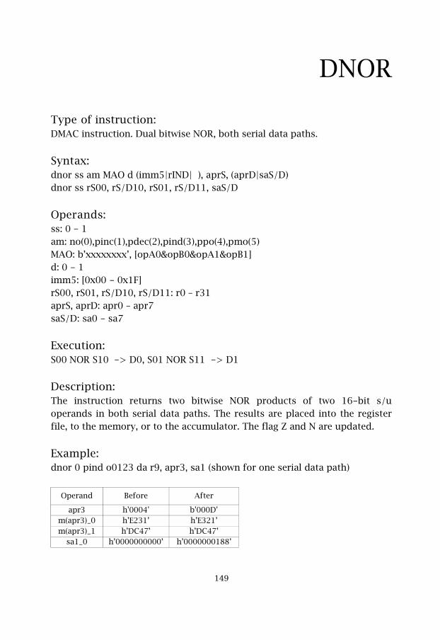
DNOR
Type of instruction:DMAC instruction. Dual bitwise NOR, both serial data paths.
Syntax:dnor ss am MAO d (imm5|rIND| ), aprS, (aprD|saS/D)dnor ss rS00, rS/D10, rS01, rS/D11, saS/D
Operands:ss: 0 - 1am: no(0),pinc(1),pdec(2),pind(3),ppo(4),pmo(5)MAO: b’xxxxxxxx’, [opA0&opB0&opA1&opB1]d: 0 - 1imm5: [0x00 - 0x1F]rS00, rS01, rS/D10, rS/D11: r0 – r31aprS, aprD: apr0 – apr7saS/D: sa0 - sa7
Execution:S00 NOR S10 -> D0, S01 NOR S11 -> D1
Description:The instruction returns two bitwise NOR products of two 16-bit s/uoperands in both serial data paths. The results are placed into the registerfile, to the memory, or to the accumulator. The flag Z and N are updated.
Example:dnor 0 pind o0123 da r9, apr3, sa1 (shown for one serial data path)
Operand Before After
apr3 h'0004' b'000D'm(apr3)_0 h’E231’ h’E321’m(apr3)_1 h’DC47’ h’DC47’
sa1_0 h’0000000000’ h’0000000188’
��
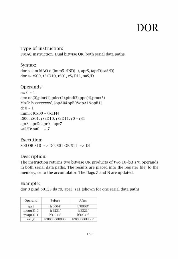
DOR
Type of instruction:DMAC instruction. Dual bitwise OR, both serial data paths.
Syntax:dor ss am MAO d (imm5|rIND| ), aprS, (aprD|saS/D)dor ss rS00, rS/D10, rS01, rS/D11, saS/D
Operands:ss: 0 - 1am: no(0),pinc(1),pdec(2),pind(3),ppo(4),pmo(5)MAO: b’xxxxxxxx’, [opA0&opB0&opA1&opB1]d: 0 - 1imm5: [0x00 - 0x1FF]rS00, rS01, rS/D10, rS/D11: r0 – r31aprS, aprD: apr0 – apr7saS/D: sa0 - sa7
Execution:S00 OR S10 -> D0, S01 OR S11 -> D1
Description:The instruction returns two bitwise OR products of two 16-bit s/u operandsin both serial data paths. The results are placed into the register file, to thememory, or to the accumulator. The flags Z and N are updated.
Example:dor 0 pind o0123 da r9, apr3, sa1 (shown for one serial data path)
Operand Before After
apr3 h'0004' b'000D'm(apr3)_0 h’E231’ h’E321’m(apr3)_1 h’DC47’ h’DC47’
sa1_0 h’0000000000’ h’000000FE77’
��(
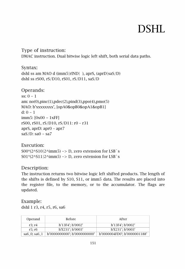
DSHL
Type of instruction:DMAC instruction. Dual bitwise logic left shift, both serial data paths.
Syntax:dshl ss am MAO d (imm5|rIND| ), aprS, (aprD|saS/D)dshl ss rS00, rS/D10, rS01, rS/D11, saS/D
Operands:ss: 0 - 1am: no(0),pinc(1),pdec(2),pind(3),ppo(4),pmo(5)MAO: b’xxxxxxxx’, [opA0&opB0&opA1&opB1]d: 0 - 1imm5: [0x00 - 1xFF]rS00, rS01, rS/D10, rS/D11: r0 – r31aprS, aprD: apr0 – apr7saS/D: sa0 - sa7
Execution:S00*(2^S10|2^imm5) -> D, zero extension for LSB`s S01*(2^S11|2^imm5) -> D, zero extension for LSB`s
Description:The instruction returns two bitwise logic left shifted products. The length ofthe shifts is defined by S10, S11, or imm5 data. The results are placed intothe register file, to the memory, or to the accumulator. The flags areupdated.
Example:dshl 1 r3, r4, r5, r6, sa6
Operand Before After
r3; r4 h'13F4'; h'0002' h'13F4'; h'0002'r5; r6 h’E231’; h'0003' h’E231’; h'0003'
sa6_0; sa6_1 h’0000000000’; h’0000000000’ h’0000004FD0’; h’0000001188’
���

DSHRA
Type of instruction:DMAC instruction. Dual bitwise arithmetic right, both serial data paths.
Syntax:dshra ss am MAO d (imm5|rIND| ), aprS, (aprD|saS/D)dshra ss rS00, rS/D10, rS01, rS/D11, saS/D
Operands:ss: 0 - 1am: no(0),pinc(1),pdec(2),pind(3),ppo(4),pmo(5)MAO: b’xxxxxxxx’, [opA0&opB0&opA1&opB1]d: 0 - 1imm5: [0x00 – 0x1F]rS00, rS01, rS/D10, rS/D11: r0 – r31aprS, aprD: apr0 – apr7saS/D: sa0 - sa7
Execution:S00/(2^S10|2^imm5) -> D, sign extension for MSB`s S01/(2^S11|2^imm5) -> D, sign extension for MSB`s
Description:The instruction returns two bitwise arithmetic right shifted products. Thelength of the shifts is defined by S10, S11, or imm5 data. The results areplaced into the register file, to the memory, or to the accumulator. The flagsZ and N are updated.
Example:dshra 1 r3, r4, r5, r6, sa6
Operand Before After
r3; r4 h'13F4'; h'0002' h'13F4'; h'0002'r5; r6 h’E231’; h'0003' h’E231’; h'0003'
sa6_0; sa6_1 h’0000000000’; h’0000000000’ h’00000004FD’; h’FFFFFFFC46’
���

DSHRL
Type of instruction:DMAC instruction. Dual bitwise logic right shift, both serial data paths.
Syntax:dshrl ss am MAO d (imm5|rIND| ), aprS, (aprD|saS/D)dshrl ss rS00, rS/D10, rS01, rS/D11, saS/D
Operands:ss: 0 - 1am: no(0),pinc(1),pdec(2),pind(3),ppo(4),pmo(5)MAO: b’xxxxxxxx’, [opA0&opB0&opA1&opB1]d: 0 - 1imm5: [0x00 - 0x1F]rS00, rS01, rS/D10, rS/D11: r0 – r31aprS, aprD: apr0 – apr7saS/D: sa0 - sa7
Execution:S00/(2^S10|2^imm5) -> D, zero extension for MSB`s S01/(2^S11|2^imm5) -> D, zero extension for MSB`s
Description:The instruction returns two bitwise logic right shifted products. The lengthof the shifts is defined by S10, S11, or imm5 data. The results are placedinto the register file, to the memory, or to the accumulator. The flags Z andN are updated.
Example:dshrl 1 r3, r4, r5, r6, sa6
Operand Before After
r3; r4 h'13F4'; h'0002' h'13F4'; h'0002'r5; r6 h’E231’; h'0003' h’E231’; h'0003'
sa6_0; sa6_1 h’0000000000’; h’0000000000’ h’00000004FD’; h’0000001C46’
���
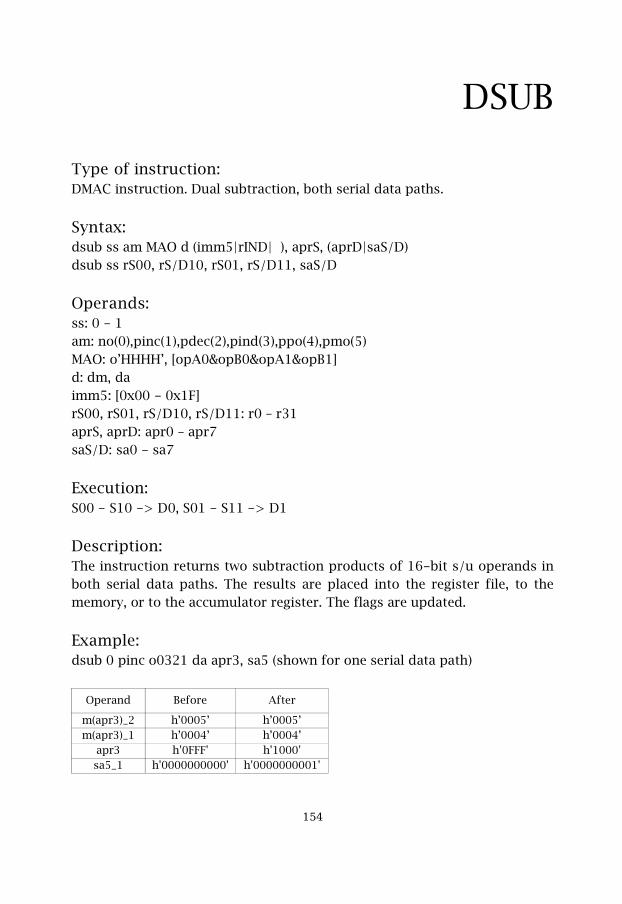
DSUB
Type of instruction:DMAC instruction. Dual subtraction, both serial data paths.
Syntax:dsub ss am MAO d (imm5|rIND| ), aprS, (aprD|saS/D)dsub ss rS00, rS/D10, rS01, rS/D11, saS/D
Operands:ss: 0 - 1am: no(0),pinc(1),pdec(2),pind(3),ppo(4),pmo(5)MAO: o’HHHH’, [opA0&opB0&opA1&opB1]d: dm, daimm5: [0x00 - 0x1F]rS00, rS01, rS/D10, rS/D11: r0 – r31aprS, aprD: apr0 – apr7saS/D: sa0 - sa7
Execution:S00 - S10 -> D0, S01 - S11 -> D1
Description:The instruction returns two subtraction products of 16-bit s/u operands inboth serial data paths. The results are placed into the register file, to thememory, or to the accumulator register. The flags are updated.
Example:dsub 0 pinc o0321 da apr3, sa5 (shown for one serial data path)
Operand Before After
m(apr3)_2 h’0005’ h’0005’m(apr3)_1 h’0004’ h’0004’
apr3 h'0FFF' h'1000'sa5_1 h'0000000000' h'0000000001'
���
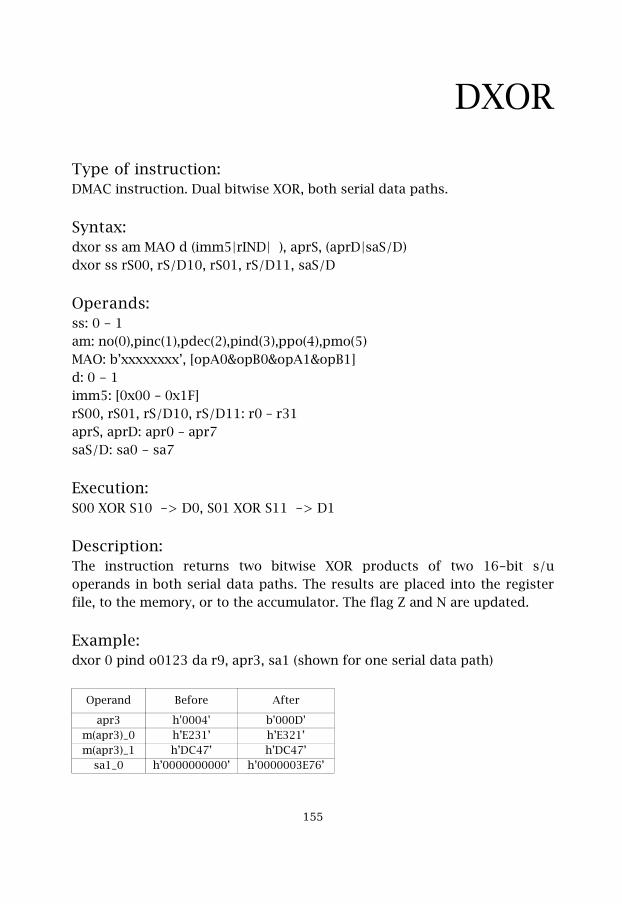
DXOR
Type of instruction:DMAC instruction. Dual bitwise XOR, both serial data paths.
Syntax:dxor ss am MAO d (imm5|rIND| ), aprS, (aprD|saS/D)dxor ss rS00, rS/D10, rS01, rS/D11, saS/D
Operands:ss: 0 - 1am: no(0),pinc(1),pdec(2),pind(3),ppo(4),pmo(5)MAO: b’xxxxxxxx’, [opA0&opB0&opA1&opB1]d: 0 - 1imm5: [0x00 – 0x1F]rS00, rS01, rS/D10, rS/D11: r0 – r31aprS, aprD: apr0 – apr7saS/D: sa0 - sa7
Execution:S00 XOR S10 -> D0, S01 XOR S11 -> D1
Description:The instruction returns two bitwise XOR products of two 16-bit s/uoperands in both serial data paths. The results are placed into the registerfile, to the memory, or to the accumulator. The flag Z and N are updated.
Example:dxor 0 pind o0123 da r9, apr3, sa1 (shown for one serial data path)
Operand Before After
apr3 h'0004' b'000D'm(apr3)_0 h’E231’ h’E321’m(apr3)_1 h’DC47’ h’DC47’
sa1_0 h’0000000000’ h’0000003E76’
���
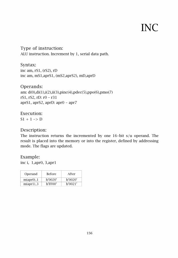
INC
Type of instruction:ALU instruction. Increment by 1, serial data path.
Syntax:inc am, rS1, (rS2), rDinc am, mS1,aprS1, (mS2,aprS2), mD,aprD
Operands: am: d(0),di(1),i(2),ii(3),pinc(4),pdec(5),ppo(6),pmo(7)rS1, rS2, rD: r0 – r31aprS1, aprS2, aprD: apr0 - apr7
Execution:S1 + 1 -> D
Description:The instruction returns the incremented by one 16-bit s/u operand. Theresult is placed into the memory or into the register, defined by addressingmode. The flags are updated.
Example:inc i, 1,apr0, 3,apr1
Operand Before After
m(apr0)_1 h’0020’ h’0020’m(apr1)_3 h’FF00’ h’0021’
���
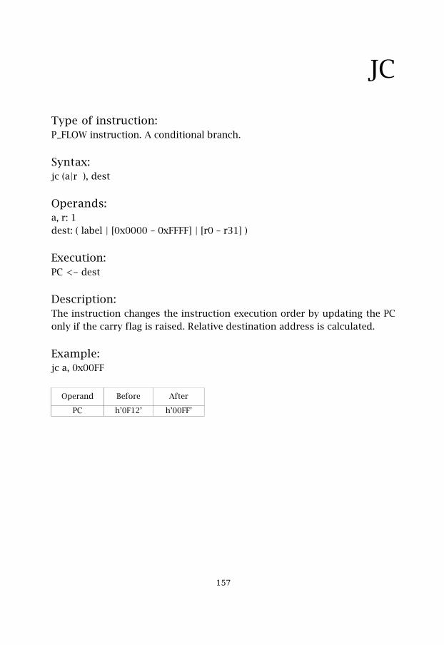
JC
Type of instruction:P_FLOW instruction. A conditional branch.
Syntax:jc (a|r ), dest
Operands:a, r: 1dest: ( label | [0x0000 – 0xFFFF] | [r0 – r31] )
Execution:PC <- dest
Description:The instruction changes the instruction execution order by updating the PConly if the carry flag is raised. Relative destination address is calculated.
Example:jc a, 0x00FF
Operand Before After
PC h’0F12’ h’00FF’
���
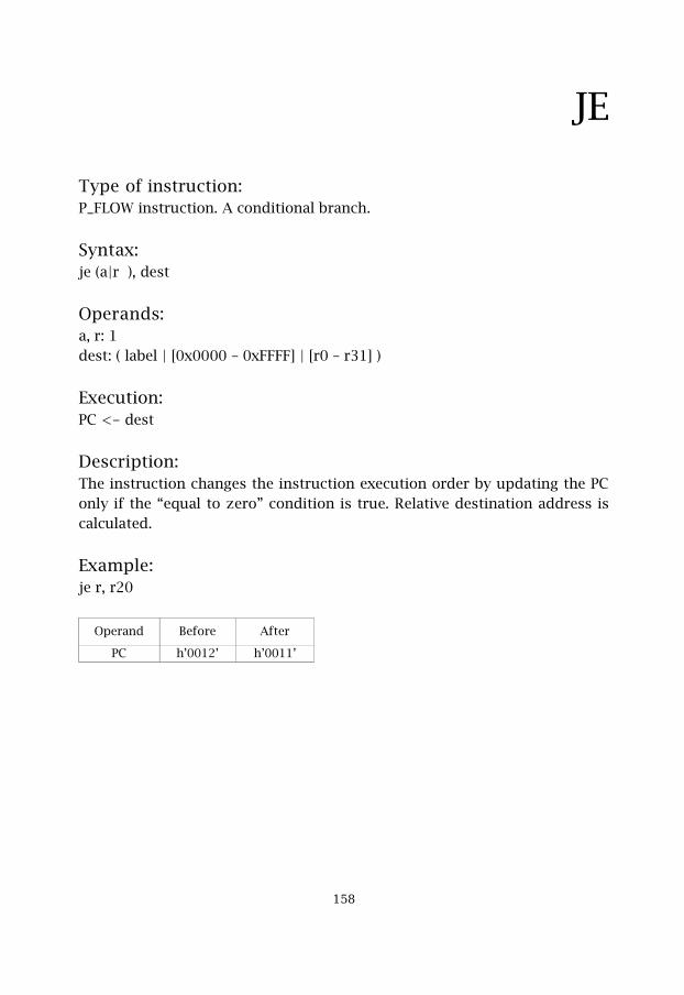
JE
Type of instruction:P_FLOW instruction. A conditional branch.
Syntax:je (a|r ), dest
Operands:a, r: 1dest: ( label | [0x0000 – 0xFFFF] | [r0 – r31] )
Execution:PC <- dest
Description:The instruction changes the instruction execution order by updating the PConly if the “equal to zero” condition is true. Relative destination address iscalculated.
Example:je r, r20
Operand Before After
PC h’0012’ h’0011’
���

JGT
Type of instruction:P_FLOW instruction. A conditional branch.
Syntax:jgt (a|r ), dest
Operands:a, r: 1dest: ( label | [0x0000 – 0xFFFF] | [r0 – r31] )
Execution:PC <- dest
Description:The instruction changes the instruction execution order by updating the PConly if the “greater then zero” condition is true. Relative destination addressis calculated.
Example:jgt loop
Operand Before After
PC h’0003’ h’000A’
��
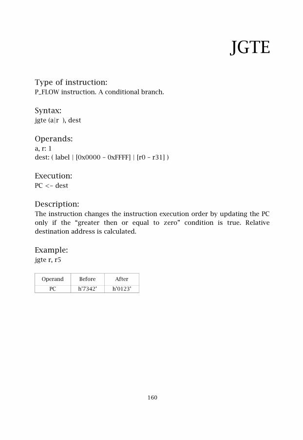
JGTE
Type of instruction:P_FLOW instruction. A conditional branch.
Syntax:jgte (a|r ), dest
Operands:a, r: 1dest: ( label | [0x0000 – 0xFFFF] | [r0 – r31] )
Execution:PC <- dest
Description:The instruction changes the instruction execution order by updating the PConly if the “greater then or equal to zero” condition is true. Relativedestination address is calculated.
Example:jgte r, r5
Operand Before After
PC h’7342’ h’0123’
��(

JLT
Type of instruction:P_FLOW instruction. A conditional branch.
Syntax:jlt (a|r ), dest
Operands:a, r: 1dest: ( label | [0x0000 – 0xFFFF] | [r0 – r31] )
Execution:PC <- dest
Description:The instruction changes the instruction execution order by updating the PConly if the “less then zero” condition is true. Relative destination address iscalculated.
Example:jlt a, 0x0211
Operand Before After
PC h’7342’ h’0211’
���
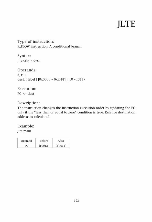
JLTE
Type of instruction:P_FLOW instruction. A conditional branch.
Syntax:jlte (a|r ), dest
Operands:a, r: 1dest: ( label | [0x0000 – 0xFFFF] | [r0 – r31] )
Execution:PC <- dest
Description:The instruction changes the instruction execution order by updating the PConly if the “less then or equal to zero” condition is true. Relative destinationaddress is calculated.
Example:jlte main
Operand Before After
PC h’0012’ h’0011’
���
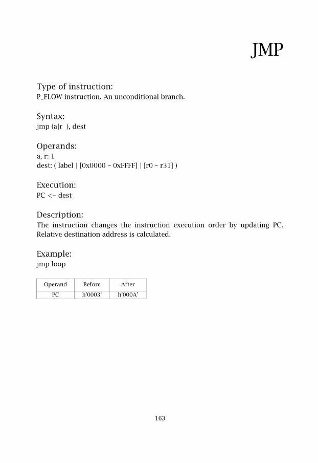
JMP
Type of instruction:P_FLOW instruction. An unconditional branch.
Syntax:jmp (a|r ), dest
Operands:a, r: 1dest: ( label | [0x0000 – 0xFFFF] | [r0 – r31] )
Execution:PC <- dest
Description:The instruction changes the instruction execution order by updating PC.Relative destination address is calculated.
Example:jmp loop
Operand Before After
PC h’0003’ h’000A’
���
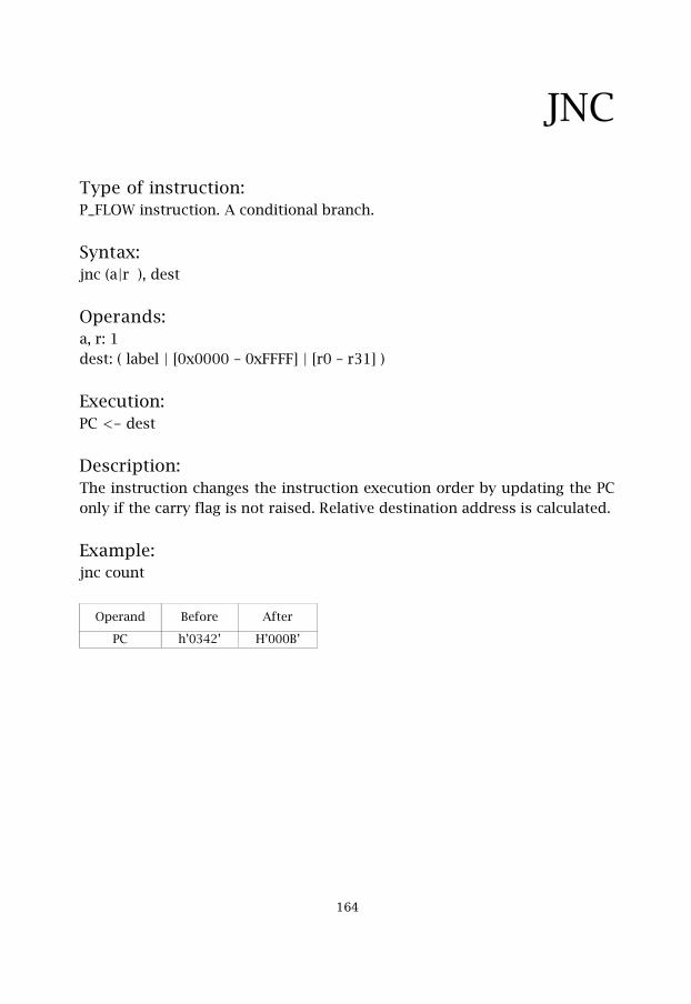
JNC
Type of instruction:P_FLOW instruction. A conditional branch.
Syntax:jnc (a|r ), dest
Operands:a, r: 1dest: ( label | [0x0000 – 0xFFFF] | [r0 – r31] )
Execution:PC <- dest
Description:The instruction changes the instruction execution order by updating the PConly if the carry flag is not raised. Relative destination address is calculated.
Example:jnc count
Operand Before After
PC h’0342’ H’000B’
���
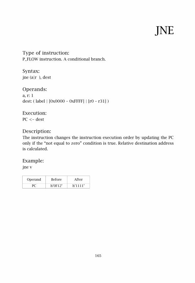
JNE
Type of instruction:P_FLOW instruction. A conditional branch.
Syntax:jne (a|r ), dest
Operands:a, r: 1dest: ( label | [0x0000 – 0xFFFF] | [r0 – r31] )
Execution:PC <- dest
Description:The instruction changes the instruction execution order by updating the PConly if the “not equal to zero” condition is true. Relative destination addressis calculated.
Example:jne v
Operand Before After
PC h’0F12’ h’1111’
���
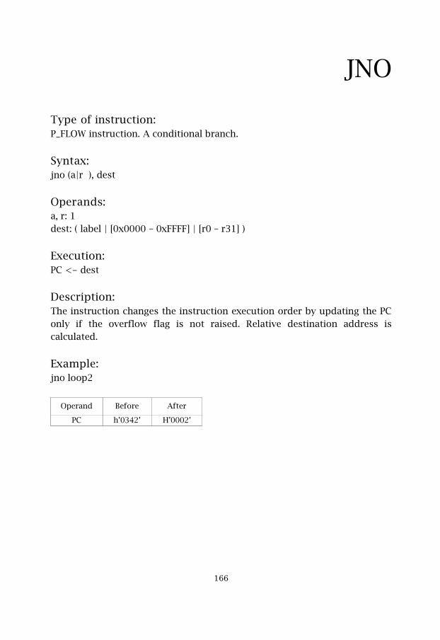
JNO
Type of instruction:P_FLOW instruction. A conditional branch.
Syntax:jno (a|r ), dest
Operands:a, r: 1dest: ( label | [0x0000 – 0xFFFF] | [r0 – r31] )
Execution:PC <- dest
Description:The instruction changes the instruction execution order by updating the PConly if the overflow flag is not raised. Relative destination address iscalculated.
Example:jno loop2
Operand Before After
PC h’0342’ H’0002’
���
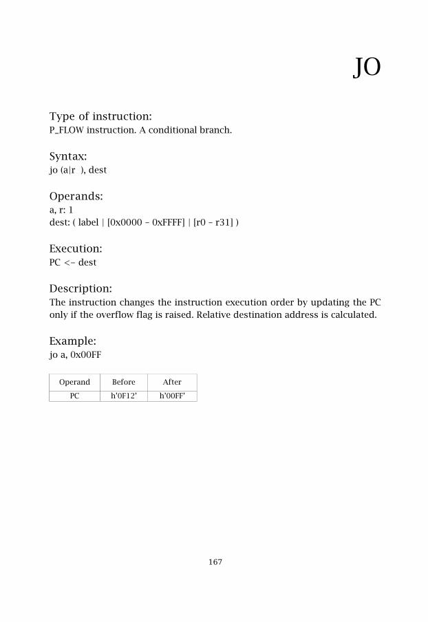
JO
Type of instruction:P_FLOW instruction. A conditional branch.
Syntax:jo (a|r ), dest
Operands:a, r: 1dest: ( label | [0x0000 – 0xFFFF] | [r0 – r31] )
Execution:PC <- dest
Description:The instruction changes the instruction execution order by updating the PConly if the overflow flag is raised. Relative destination address is calculated.
Example:jo a, 0x00FF
Operand Before After
PC h’0F12’ h’00FF’
���
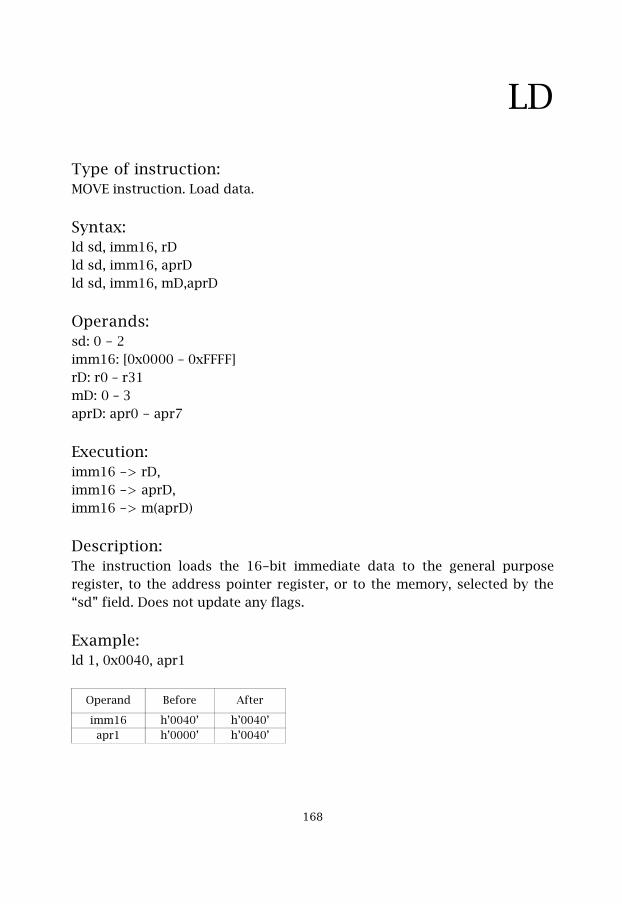
LD
Type of instruction:MOVE instruction. Load data.
Syntax:ld sd, imm16, rDld sd, imm16, aprDld sd, imm16, mD,aprD
Operands: sd: 0 - 2imm16: [0x0000 – 0xFFFF]rD: r0 – r31mD: 0 – 3aprD: apr0 - apr7
Execution:imm16 -> rD,imm16 -> aprD,imm16 -> m(aprD)
Description:The instruction loads the 16-bit immediate data to the general purposeregister, to the address pointer register, or to the memory, selected by the“sd” field. Does not update any flags.
Example:ld 1, 0x0040, apr1
Operand Before After
imm16 h’0040’ h’0040’apr1 h’0000’ h’0040’
���
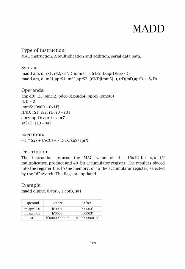
MADD
Type of instruction:MAC instruction. A Multiplication and addition, serial data path.
Syntax:madd am, d, rS1, rS2, (rIND|imm5| ), (rD|mD,aprD|saS/D)madd am, d, mS1,aprS1, mS2,aprS2, (rIND|imm5| ), (rD|mD,aprD|saS/D)
Operands: am: d(0),i(1),pinc(2),pdec(3),pind(4),ppo(5),pmo(6)d: 0 - 2imm5: [0x00 – 0x1F]rIND, rS1, rS2, rD: r0 – r31aprS, aprD: apr0 - apr7saS/D: sa0 – sa7
Execution:(S1 * S2) + [ACC] -> D(rX/saX/aprX)
Description:The instruction returns the MAC value of the 16x16-bit s/u i/fmultiplication product and 40-bit accumulator register. The result is placedinto the register file, to the memory, or to the accumulator register, selectedby the “d” switch. The flags are updated.
Example:madd d,pinc, 0,apr3, 1,apr3, sa1
Operand Before After
m(apr3)_0 h‘0004’ h’0004’m(apr3)_1 h’0003’ h’0003’
sa1 h’0000000007’ h’0000000013’
��
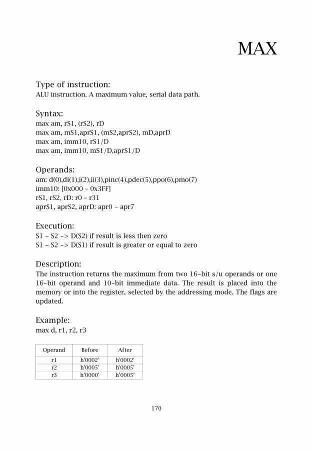
MAX
Type of instruction:ALU instruction. A maximum value, serial data path.
Syntax:max am, rS1, (rS2), rDmax am, mS1,aprS1, (mS2,aprS2), mD,aprDmax am, imm10, rS1/Dmax am, imm10, mS1/D,aprS1/D
Operands: am: d(0),di(1),i(2),ii(3),pinc(4),pdec(5),ppo(6),pmo(7)imm10: [0x000 – 0x3FF]rS1, rS2, rD: r0 – r31aprS1, aprS2, aprD: apr0 - apr7
Execution:S1 - S2 -> D(S2) if result is less then zeroS1 - S2 -> D(S1) if result is greater or equal to zero
Description:The instruction returns the maximum from two 16-bit s/u operands or one16-bit operand and 10-bit immediate data. The result is placed into thememory or into the register, selected by the addressing mode. The flags areupdated.
Example:max d, r1, r2, r3
Operand Before After
r1 h'0002' h'0002'r2 h'0005' h'0005'r3 h’0000’ h’0005’
��(
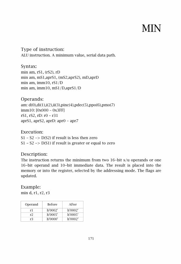
MIN
Type of instruction:ALU instruction. A minimum value, serial data path.
Syntax:min am, rS1, (rS2), rDmin am, mS1,aprS1, (mS2,aprS2), mD,aprDmin am, imm10, rS1/Dmin am, imm10, mS1/D,aprS1/D
Operands: am: d(0),di(1),i(2),ii(3),pinc(4),pdec(5),ppo(6),pmo(7)imm10: [0x000 – 0x3FF]rS1, rS2, rD: r0 – r31aprS1, aprS2, aprD: apr0 - apr7
Execution:S1 - S2 -> D(S2) if result is less then zeroS1 - S2 -> D(S1) if result is greater or equal to zero
Description:The instruction returns the minimum from two 16-bit s/u operands or one16-bit operand and 10-bit immediate data. The result is placed into thememory or into the register, selected by the addressing mode. The flags areupdated.
Example:min d, r1, r2, r3
Operand Before After
r1 h'0002' h'0002'r2 h'0005' h'0005'r3 h’0000’ h’0002’
���
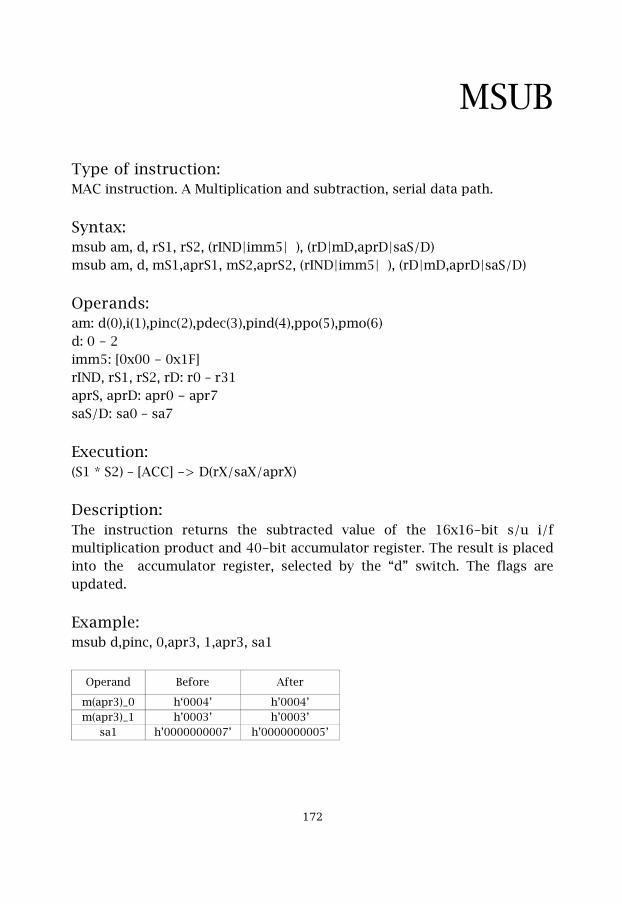
MSUB
Type of instruction:MAC instruction. A Multiplication and subtraction, serial data path.
Syntax:msub am, d, rS1, rS2, (rIND|imm5| ), (rD|mD,aprD|saS/D)msub am, d, mS1,aprS1, mS2,aprS2, (rIND|imm5| ), (rD|mD,aprD|saS/D)
Operands: am: d(0),i(1),pinc(2),pdec(3),pind(4),ppo(5),pmo(6)d: 0 - 2imm5: [0x00 - 0x1F]rIND, rS1, rS2, rD: r0 – r31aprS, aprD: apr0 - apr7saS/D: sa0 – sa7
Execution:(S1 * S2) – [ACC] -> D(rX/saX/aprX)
Description:The instruction returns the subtracted value of the 16x16-bit s/u i/fmultiplication product and 40-bit accumulator register. The result is placedinto the accumulator register, selected by the “d” switch. The flags areupdated.
Example:msub d,pinc, 0,apr3, 1,apr3, sa1
Operand Before After
m(apr3)_0 h‘0004’ h’0004’m(apr3)_1 h’0003’ h’0003’
sa1 h’0000000007’ h’0000000005’
���
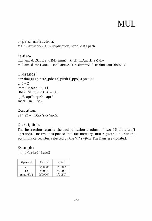
MUL
Type of instruction:MAC instruction. A multiplication, serial data path.
Syntax:mul am, d, rS1, rS2, (rIND|imm5| ), (rD|mD,aprD|saS/D)mul am, d, mS1,aprS1, mS2,aprS2, (rIND|imm5| ), (rD|mD,aprD|saS/D)
Operands: am: d(0),i(1),pinc(2),pdec(3),pind(4),ppo(5),pmo(6)d: 0 - 2imm5: [0x00 -0x1F]rIND, rS1, rS2, rD: r0 – r31aprS, aprD: apr0 - apr7saS/D: sa0 – sa7
Execution:S1 * S2 -> D(rX/saX/aprX)
Description:The instruction returns the multiplication product of two 16-bit s/u i/foperands. The result is placed into the memory, into register file or in theaccumulator register, selected by the “d” switch. The flags are updated.
Example:mul d,0, r1,r2, 2,apr3
Operand Before After
r1 h‘0008’ h’0008’r2 h’000F’ h’000F’
m(apr3)_2 h’0000’ h’00F0’
���
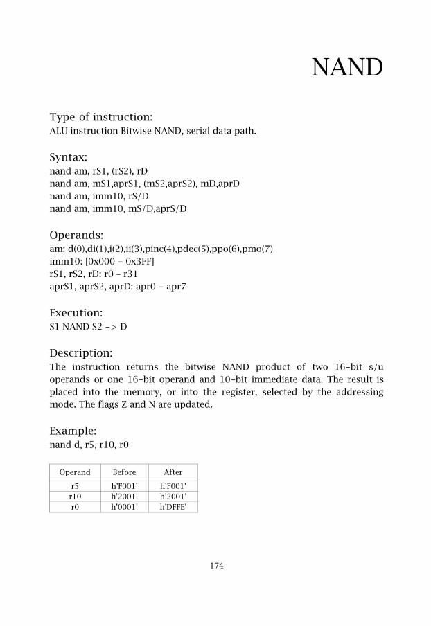
NAND
Type of instruction:ALU instruction Bitwise NAND, serial data path.
Syntax:nand am, rS1, (rS2), rDnand am, mS1,aprS1, (mS2,aprS2), mD,aprDnand am, imm10, rS/Dnand am, imm10, mS/D,aprS/D
Operands:am: d(0),di(1),i(2),ii(3),pinc(4),pdec(5),ppo(6),pmo(7)imm10: [0x000 - 0x3FF]rS1, rS2, rD: r0 – r31aprS1, aprS2, aprD: apr0 - apr7
Execution:S1 NAND S2 -> D
Description:The instruction returns the bitwise NAND product of two 16-bit s/uoperands or one 16-bit operand and 10-bit immediate data. The result isplaced into the memory, or into the register, selected by the addressingmode. The flags Z and N are updated.
Example:nand d, r5, r10, r0
Operand Before After
r5 h’F001’ h’F001’r10 h’2001’ h’2001’r0 h’0001’ h’DFFE’
���
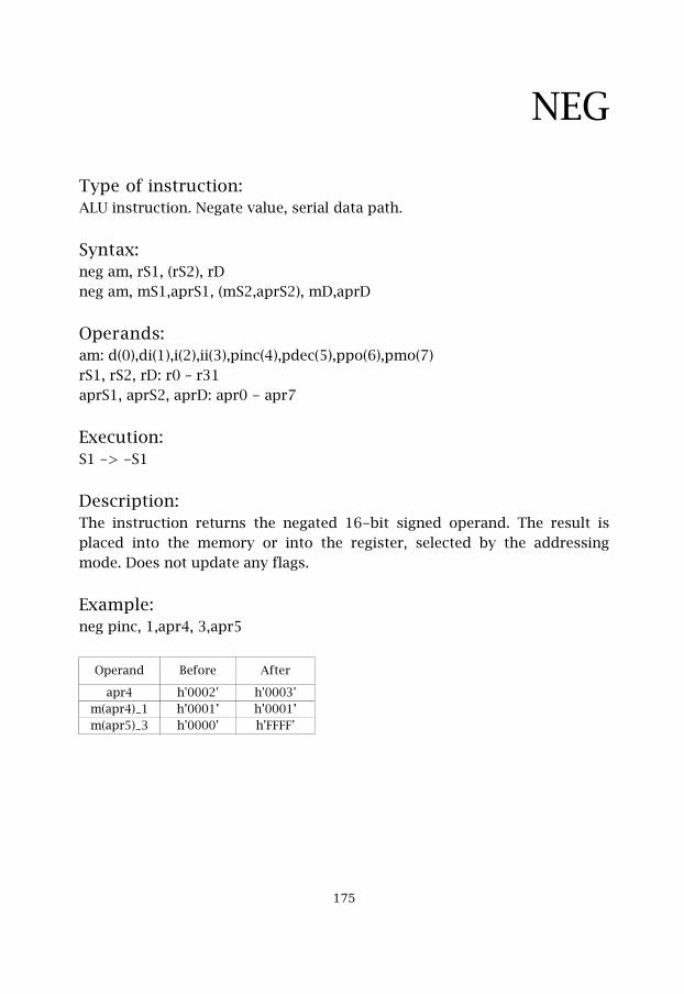
NEG
Type of instruction:ALU instruction. Negate value, serial data path.
Syntax:neg am, rS1, (rS2), rDneg am, mS1,aprS1, (mS2,aprS2), mD,aprD
Operands: am: d(0),di(1),i(2),ii(3),pinc(4),pdec(5),ppo(6),pmo(7)rS1, rS2, rD: r0 – r31aprS1, aprS2, aprD: apr0 - apr7
Execution:S1 -> -S1
Description:The instruction returns the negated 16-bit signed operand. The result isplaced into the memory or into the register, selected by the addressingmode. Does not update any flags.
Example:neg pinc, 1,apr4, 3,apr5
Operand Before After
apr4 h'0002' h'0003'm(apr4)_1 h’0001’ h’0001’m(apr5)_3 h'0000' h'FFFF'
���
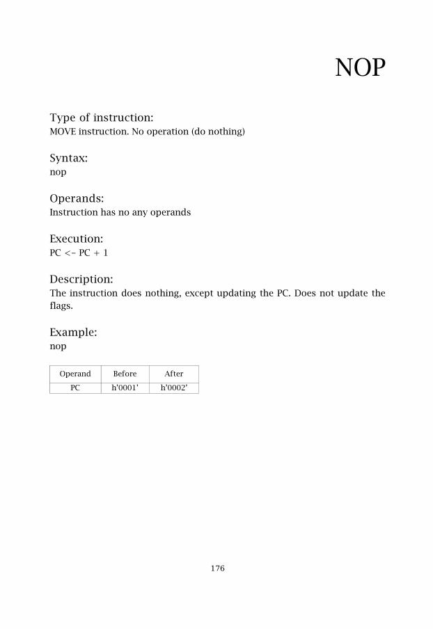
NOP
Type of instruction:MOVE instruction. No operation (do nothing)
Syntax:nop
Operands: Instruction has no any operands
Execution:PC <- PC + 1
Description:The instruction does nothing, except updating the PC. Does not update theflags.
Example:nop
Operand Before After
PC h’0001’ h’0002’
���
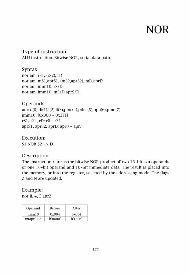
NOR
Type of instruction:ALU instruction. Bitwise NOR, serial data path.
Syntax:nor am, rS1, (rS2), rDnor am, mS1,aprS1, (mS2,aprS2), mD,aprDnor am, imm10, rS/Dnor am, imm10, mS/D,aprS/D
Operands: am: d(0),di(1),i(2),ii(3),pinc(4),pdec(5),ppo(6),pmo(7)imm10: [0x000 - 0x3FF]rS1, rS2, rD: r0 – r31aprS1, aprS2, aprD: apr0 - apr7
Execution:S1 NOR S2 -> D
Description:The instruction returns the bitwise NOR product of two 16-bit s/u operandsor one 16-bit operand and 10-bit immediate data. The result is placed intothe memory, or into the register, selected by the addressing mode. The flagsZ and N are updated.
Example:nor ii, 4, 2,apr2
Operand Before After
imm10 0x004 0x004m(apr2)_2 h’0000’ h’FFFB’
���
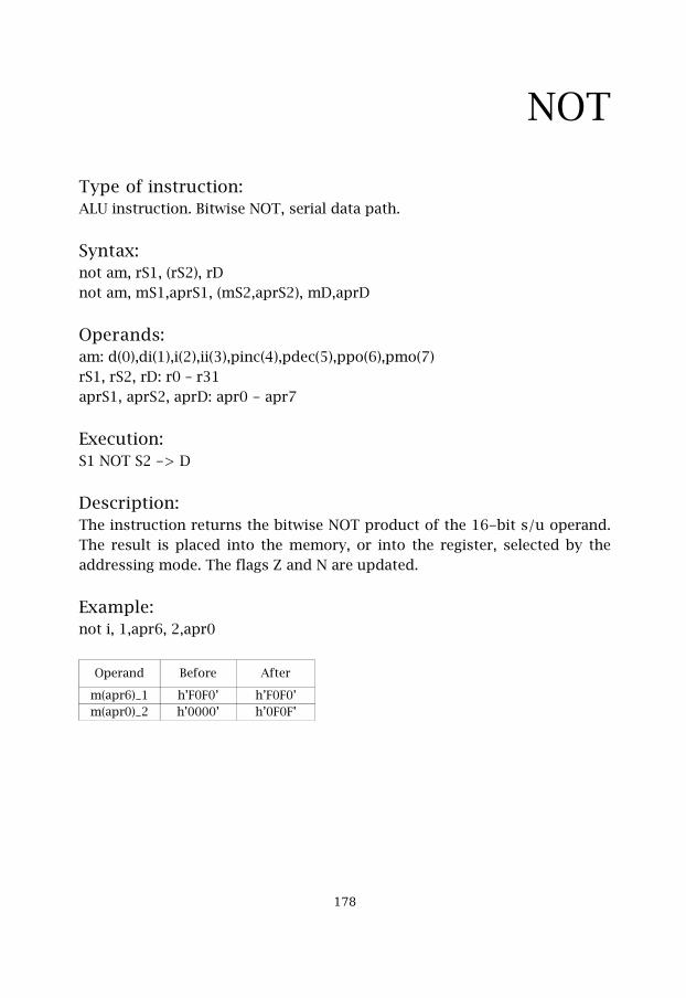
NOT
Type of instruction:ALU instruction. Bitwise NOT, serial data path.
Syntax:not am, rS1, (rS2), rDnot am, mS1,aprS1, (mS2,aprS2), mD,aprD
Operands: am: d(0),di(1),i(2),ii(3),pinc(4),pdec(5),ppo(6),pmo(7)rS1, rS2, rD: r0 – r31aprS1, aprS2, aprD: apr0 - apr7
Execution:S1 NOT S2 -> D
Description:The instruction returns the bitwise NOT product of the 16-bit s/u operand.The result is placed into the memory, or into the register, selected by theaddressing mode. The flags Z and N are updated.
Example:not i, 1,apr6, 2,apr0
Operand Before After
m(apr6)_1 h’F0F0’ h’F0F0’m(apr0)_2 h’0000’ h’0F0F’
���
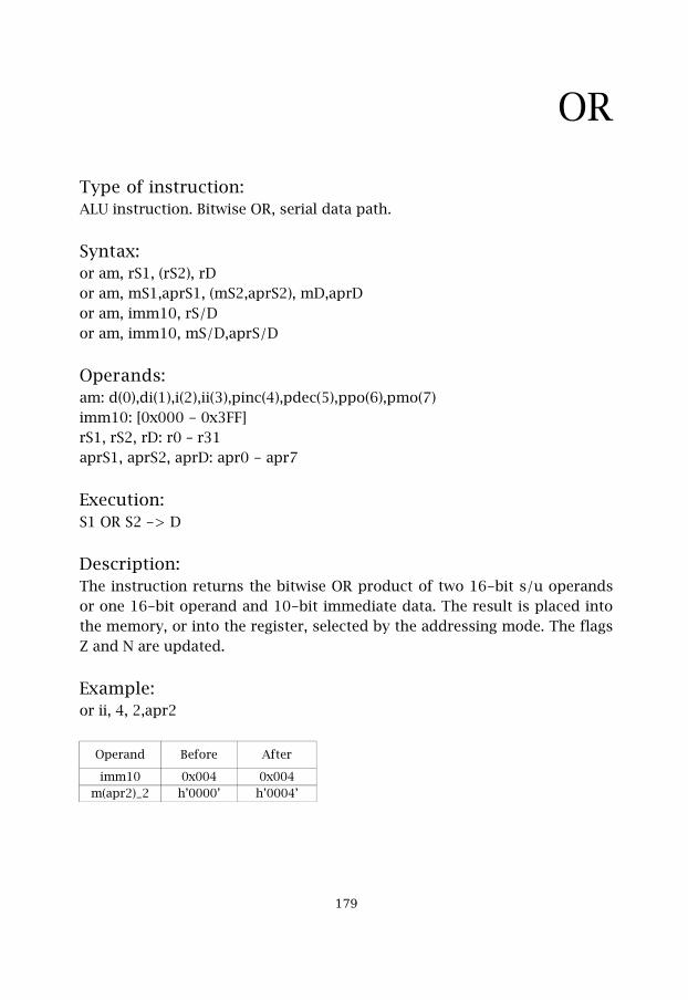
OR
Type of instruction:ALU instruction. Bitwise OR, serial data path.
Syntax:or am, rS1, (rS2), rDor am, mS1,aprS1, (mS2,aprS2), mD,aprDor am, imm10, rS/Dor am, imm10, mS/D,aprS/D
Operands: am: d(0),di(1),i(2),ii(3),pinc(4),pdec(5),ppo(6),pmo(7)imm10: [0x000 - 0x3FF]rS1, rS2, rD: r0 – r31aprS1, aprS2, aprD: apr0 - apr7
Execution:S1 OR S2 -> D
Description:The instruction returns the bitwise OR product of two 16-bit s/u operandsor one 16-bit operand and 10-bit immediate data. The result is placed intothe memory, or into the register, selected by the addressing mode. The flagsZ and N are updated.
Example:or ii, 4, 2,apr2
Operand Before After
imm10 0x004 0x004m(apr2)_2 h’0000’ h’0004’
��

PADD
Type of instruction:SIMD instruction. An addition, parallel data paths.
Syntax:padd am ip MAO d aprS, (aprD|paS/paD)padd am ip MAO d imm5, aprS, (aprD|paS/paD)padd am ip MAO d rIND, aprS, (aprD|paS/paD)
Operands: am: no(0),pinc(1),pdec(2),pind(3),ppo(4),pmo(5)ip: sp, dpMAO: o’HHHH’d: da, dmimm5: [0x00 - 0x1F]rIND: r0 – r31aprS, aprD: apr0 - apr7paS, paD: pa0 – pa7
Execution:S1(aprS) + S2(aprS) -> D(aprD/paD)
Description:The instruction returns the sum of two 8/16-bit s/u operands. The result isplaced into the memory or into the accumulator register, selected by the“d” switch. The flags are updated.
Example:padd pinc sp o0231 da apr0, pa3 (shown for one parallel data path)
Operand Before After
apr0 h‘0000’ h’0001’m(apr0)_2 h’0110’ h’0110’
pa3_2 h’00000’ h’00011’
��(
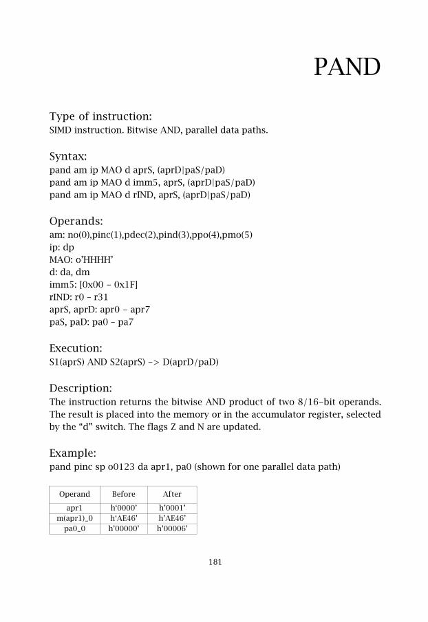
PAND
Type of instruction:SIMD instruction. Bitwise AND, parallel data paths.
Syntax:pand am ip MAO d aprS, (aprD|paS/paD)pand am ip MAO d imm5, aprS, (aprD|paS/paD)pand am ip MAO d rIND, aprS, (aprD|paS/paD)
Operands: am: no(0),pinc(1),pdec(2),pind(3),ppo(4),pmo(5)ip: dpMAO: o’HHHH’d: da, dmimm5: [0x00 - 0x1F]rIND: r0 – r31aprS, aprD: apr0 - apr7paS, paD: pa0 – pa7
Execution:S1(aprS) AND S2(aprS) -> D(aprD/paD)
Description:The instruction returns the bitwise AND product of two 8/16-bit operands.The result is placed into the memory or in the accumulator register, selectedby the “d” switch. The flags Z and N are updated.
Example:pand pinc sp o0123 da apr1, pa0 (shown for one parallel data path)
Operand Before After
apr1 h‘0000’ h’0001’m(apr1)_0 h‘AE46’ h’AE46’
pa0_0 h’00000’ h’00006’
���
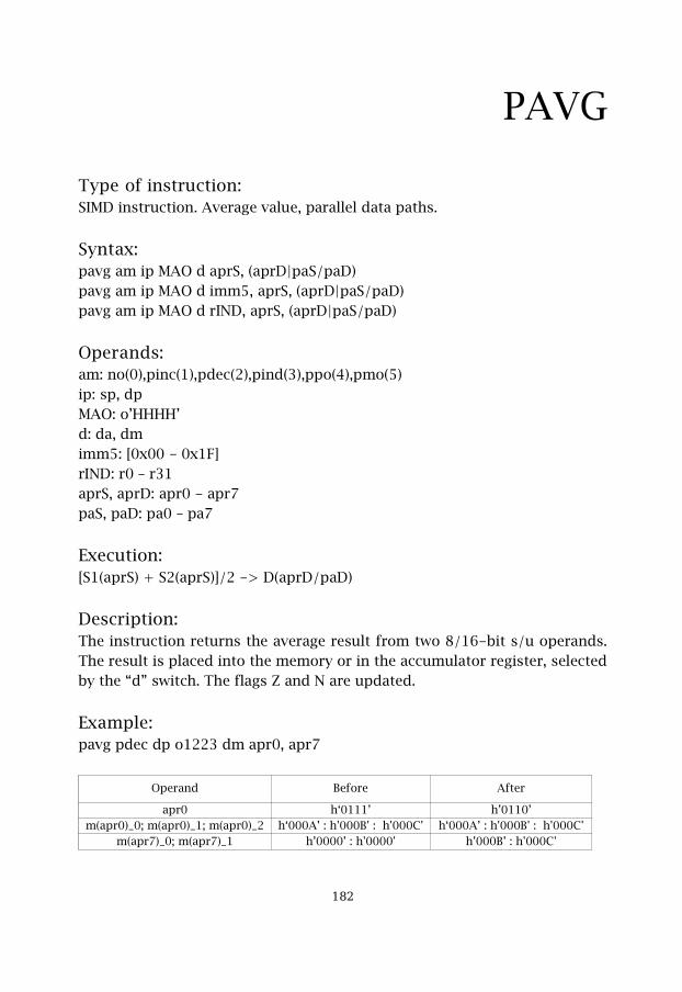
PAVG
Type of instruction:SIMD instruction. Average value, parallel data paths.
Syntax:pavg am ip MAO d aprS, (aprD|paS/paD)pavg am ip MAO d imm5, aprS, (aprD|paS/paD)pavg am ip MAO d rIND, aprS, (aprD|paS/paD)
Operands: am: no(0),pinc(1),pdec(2),pind(3),ppo(4),pmo(5)ip: sp, dpMAO: o’HHHH’d: da, dmimm5: [0x00 - 0x1F]rIND: r0 – r31aprS, aprD: apr0 - apr7paS, paD: pa0 – pa7
Execution:[S1(aprS) + S2(aprS)]/2 -> D(aprD/paD)
Description:The instruction returns the average result from two 8/16-bit s/u operands.The result is placed into the memory or in the accumulator register, selectedby the “d” switch. The flags Z and N are updated.
Example:pavg pdec dp o1223 dm apr0, apr7
Operand Before After
apr0 h‘0111’ h’0110’m(apr0)_0; m(apr0)_1; m(apr0)_2 h‘000A’ : h'000B' : h'000C' h‘000A’ : h'000B' : h'000C'
m(apr7)_0; m(apr7)_1 h’0000’ : h'0000' h’000B’ : h'000C'
���

PCMPE
Type of instruction:SIMD instruction. Compare to zero, parallel data paths.
Syntax:pcmpe am ip MAO d aprS, (aprD|paS/paD)pcmpe am ip MAO d imm5, aprS, (aprD|paS/paD)pcmpe am ip MAO d rIND, aprS, (aprD|paS/paD)
Operands: am: no(0),pinc(1),pdec(2),pind(3),ppo(4),pmo(5)ip: dpMAO: o’HHHH’d: da, dmimm5: [0x00 - 0x1F]rIND: r0 – r31aprS, aprD: apr0 - apr7paS, paD: pa0 – pa7
Execution:0 <- if opA != opB , 1 <- if opA = opB
Description:The instruction returns one if two 8/16-bit s/u operands are equal, andzero otherwise. The result is placed into the memory or in the accumulatorregister, selected by the “d” switch. The flags O and C are updated.
Example:pcmpe pinc dp o2211 da apr1, pa0 (shown for one parallel data path)
Operand Before After
apr1 h‘0001’ h’0002’m(apr1)_1 h‘0000’ h’0000’m(apr1)_2 h‘0000’ h’0000’
pa0_2 h’00000’ h’00001’
���
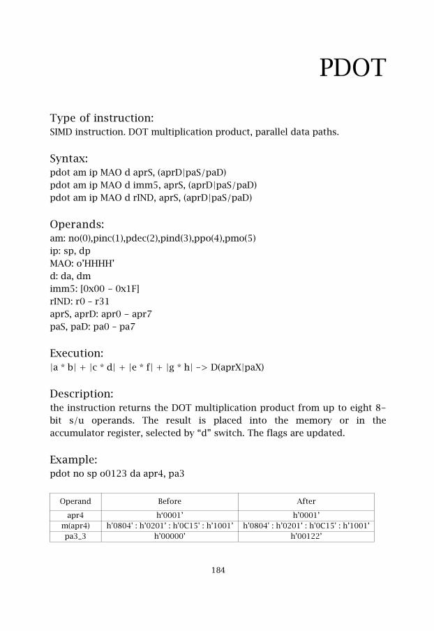
PDOT
Type of instruction:SIMD instruction. DOT multiplication product, parallel data paths.
Syntax:pdot am ip MAO d aprS, (aprD|paS/paD)pdot am ip MAO d imm5, aprS, (aprD|paS/paD)pdot am ip MAO d rIND, aprS, (aprD|paS/paD)
Operands: am: no(0),pinc(1),pdec(2),pind(3),ppo(4),pmo(5)ip: sp, dpMAO: o’HHHH’d: da, dmimm5: [0x00 - 0x1F]rIND: r0 – r31aprS, aprD: apr0 - apr7paS, paD: pa0 – pa7
Execution:|a * b| + |c * d| + |e * f| + |g * h| -> D(aprX|paX)
Description:the instruction returns the DOT multiplication product from up to eight 8-bit s/u operands. The result is placed into the memory or in theaccumulator register, selected by “d” switch. The flags are updated.
Example:pdot no sp o0123 da apr4, pa3
Operand Before After
apr4 h‘0001’ h’0001’m(apr4) h'0804' : h’0201’ : h'0C15' : h’1001’ h'0804' : h’0201’ : h'0C15' : h’1001’pa3_3 h’00000’ h’00122’
���
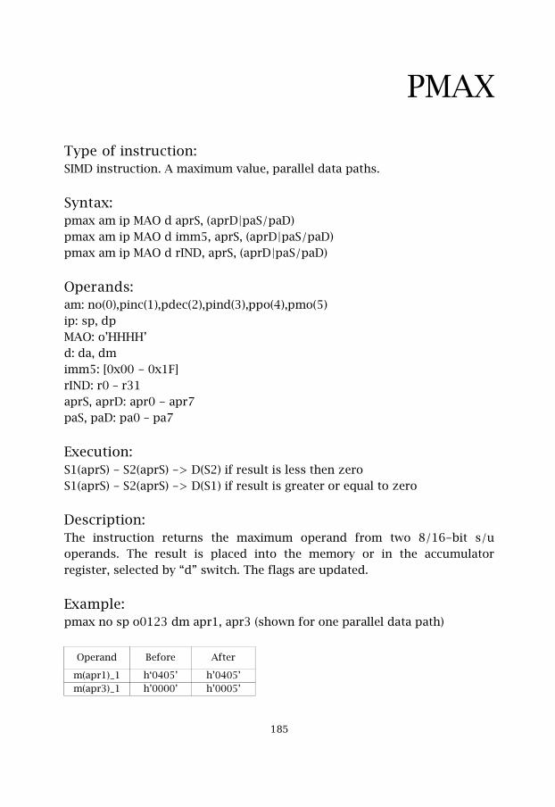
PMAX
Type of instruction:SIMD instruction. A maximum value, parallel data paths.
Syntax:pmax am ip MAO d aprS, (aprD|paS/paD)pmax am ip MAO d imm5, aprS, (aprD|paS/paD)pmax am ip MAO d rIND, aprS, (aprD|paS/paD)
Operands: am: no(0),pinc(1),pdec(2),pind(3),ppo(4),pmo(5)ip: sp, dpMAO: o’HHHH’d: da, dmimm5: [0x00 - 0x1F]rIND: r0 – r31aprS, aprD: apr0 - apr7paS, paD: pa0 – pa7
Execution:S1(aprS) - S2(aprS) -> D(S2) if result is less then zeroS1(aprS) - S2(aprS) -> D(S1) if result is greater or equal to zero
Description:The instruction returns the maximum operand from two 8/16-bit s/uoperands. The result is placed into the memory or in the accumulatorregister, selected by “d” switch. The flags are updated.
Example:pmax no sp o0123 dm apr1, apr3 (shown for one parallel data path)
Operand Before After
m(apr1)_1 h‘0405’ h’0405’m(apr3)_1 h’0000’ h’0005’
���
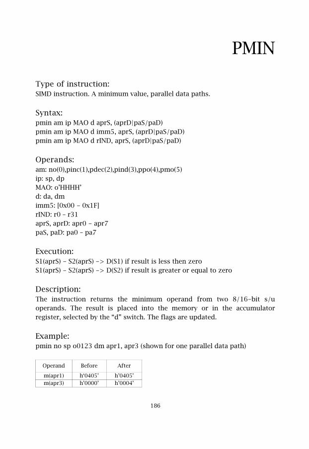
PMIN
Type of instruction:SIMD instruction. A minimum value, parallel data paths.
Syntax:pmin am ip MAO d aprS, (aprD|paS/paD)pmin am ip MAO d imm5, aprS, (aprD|paS/paD)pmin am ip MAO d rIND, aprS, (aprD|paS/paD)
Operands: am: no(0),pinc(1),pdec(2),pind(3),ppo(4),pmo(5)ip: sp, dpMAO: o’HHHH’d: da, dmimm5: [0x00 - 0x1F]rIND: r0 – r31aprS, aprD: apr0 - apr7paS, paD: pa0 – pa7
Execution:S1(aprS) - S2(aprS) -> D(S1) if result is less then zeroS1(aprS) - S2(aprS) -> D(S2) if result is greater or equal to zero
Description:The instruction returns the minimum operand from two 8/16-bit s/uoperands. The result is placed into the memory or in the accumulatorregister, selected by the “d” switch. The flags are updated.
Example:pmin no sp o0123 dm apr1, apr3 (shown for one parallel data path)
Operand Before After
m(apr1) h‘0405’ h’0405’m(apr3) h’0000’ h’0004’
���

PMUL
Type of instruction:SIMD instruction. A Multiplication, parallel data paths.
Syntax:pmul am ip MAO d aprS, (aprD|paS/paD)pmul am ip MAO d imm5, aprS, (aprD|paS/paD)pmul am ip MAO d rIND, aprS, (aprD|paS/paD)
Operands: am: no(0),pinc(1),pdec(2),pind(3),ppo(4),pmo(5)ip: sp, dpMAO: o’HHHH’d: da, dmimm5: [0x00 -0x1F]rIND: r0 – r31aprS, aprD: apr0 - apr7paS, paD: pa0 – pa7
Execution:S1(aprS) * S2(aprS) -> D(aprD/paD)
Description:The instruction returns the multiplication result of two 8/16-bit s/u i/foperands. The result is placed into the memory or in the accumulatorregister, selected by the “d” switch. The flags are updated.
Example:pmul no sp o0231 da apr4, pa3 (shown for one parallel data path)
Operand Before After
apr4 h‘0001’ h’0001’m(apr4)_3 h’0201’ h’0201’
pa3_3 h’00000’ h’00002’
���
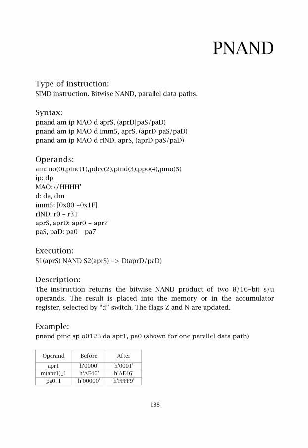
PNAND
Type of instruction:SIMD instruction. Bitwise NAND, parallel data paths.
Syntax:pnand am ip MAO d aprS, (aprD|paS/paD)pnand am ip MAO d imm5, aprS, (aprD|paS/paD)pnand am ip MAO d rIND, aprS, (aprD|paS/paD)
Operands: am: no(0),pinc(1),pdec(2),pind(3),ppo(4),pmo(5)ip: dpMAO: o’HHHH’d: da, dmimm5: [0x00 -0x1F]rIND: r0 – r31aprS, aprD: apr0 - apr7paS, paD: pa0 – pa7
Execution:S1(aprS) NAND S2(aprS) -> D(aprD/paD)
Description:The instruction returns the bitwise NAND product of two 8/16-bit s/uoperands. The result is placed into the memory or in the accumulatorregister, selected by “d” switch. The flags Z and N are updated.
Example:pnand pinc sp o0123 da apr1, pa0 (shown for one parallel data path)
Operand Before After
apr1 h‘0000’ h’0001’m(apr1)_1 h‘AE46’ h’AE46’
pa0_1 h’00000’ h’FFFF9’
���
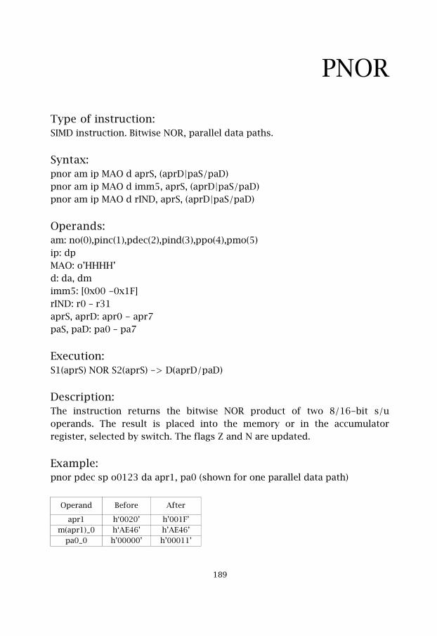
PNOR
Type of instruction:SIMD instruction. Bitwise NOR, parallel data paths.
Syntax:pnor am ip MAO d aprS, (aprD|paS/paD)pnor am ip MAO d imm5, aprS, (aprD|paS/paD)pnor am ip MAO d rIND, aprS, (aprD|paS/paD)
Operands: am: no(0),pinc(1),pdec(2),pind(3),ppo(4),pmo(5)ip: dpMAO: o’HHHH’d: da, dmimm5: [0x00 -0x1F]rIND: r0 – r31aprS, aprD: apr0 - apr7paS, paD: pa0 – pa7
Execution:S1(aprS) NOR S2(aprS) -> D(aprD/paD)
Description:The instruction returns the bitwise NOR product of two 8/16-bit s/uoperands. The result is placed into the memory or in the accumulatorregister, selected by switch. The flags Z and N are updated.
Example:pnor pdec sp o0123 da apr1, pa0 (shown for one parallel data path)
Operand Before After
apr1 h‘0020’ h’001F’m(apr1)_0 h‘AE46’ h’AE46’
pa0_0 h’00000’ h’00011’
��
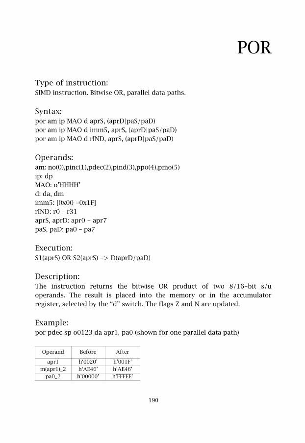
POR
Type of instruction:SIMD instruction. Bitwise OR, parallel data paths.
Syntax:por am ip MAO d aprS, (aprD|paS/paD)por am ip MAO d imm5, aprS, (aprD|paS/paD)por am ip MAO d rIND, aprS, (aprD|paS/paD)
Operands: am: no(0),pinc(1),pdec(2),pind(3),ppo(4),pmo(5)ip: dpMAO: o’HHHH’d: da, dmimm5: [0x00 -0x1F]rIND: r0 – r31aprS, aprD: apr0 - apr7paS, paD: pa0 – pa7
Execution:S1(aprS) OR S2(aprS) -> D(aprD/paD)
Description:The instruction returns the bitwise OR product of two 8/16-bit s/uoperands. The result is placed into the memory or in the accumulatorregister, selected by the “d” switch. The flags Z and N are updated.
Example:por pdec sp o0123 da apr1, pa0�(shown for one parallel data path)
Operand Before After
apr1 h‘0020’ h’001F’m(apr1)_2 h‘AE46’ h’AE46’
pa0_2 h’00000’ h’FFFEE’
�(
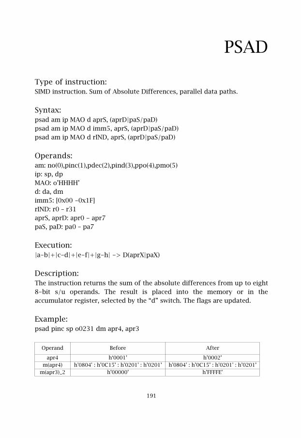
PSAD
Type of instruction:SIMD instruction. Sum of Absolute Differences, parallel data paths.
Syntax:psad am ip MAO d aprS, (aprD|paS/paD)psad am ip MAO d imm5, aprS, (aprD|paS/paD)psad am ip MAO d rIND, aprS, (aprD|paS/paD)
Operands: am: no(0),pinc(1),pdec(2),pind(3),ppo(4),pmo(5)ip: sp, dpMAO: o’HHHH’d: da, dmimm5: [0x00 -0x1F]rIND: r0 – r31aprS, aprD: apr0 - apr7paS, paD: pa0 – pa7
Execution:|a-b|+|c-d|+|e-f|+|g-h| -> D(aprX|paX)
Description:The instruction returns the sum of the absolute differences from up to eight8-bit s/u operands. The result is placed into the memory or in theaccumulator register, selected by the “d” switch. The flags are updated.
Example:psad pinc sp o0231 dm apr4, apr3
Operand Before After
apr4 h‘0001’ h’0002’m(apr4) h'0804' : h’0C15’ : h'0201' : h’0201’ h'0804' : h’0C15’ : h'0201' : h’0201’
m(apr3)_2 h’00000’ h’FFFFE’
��
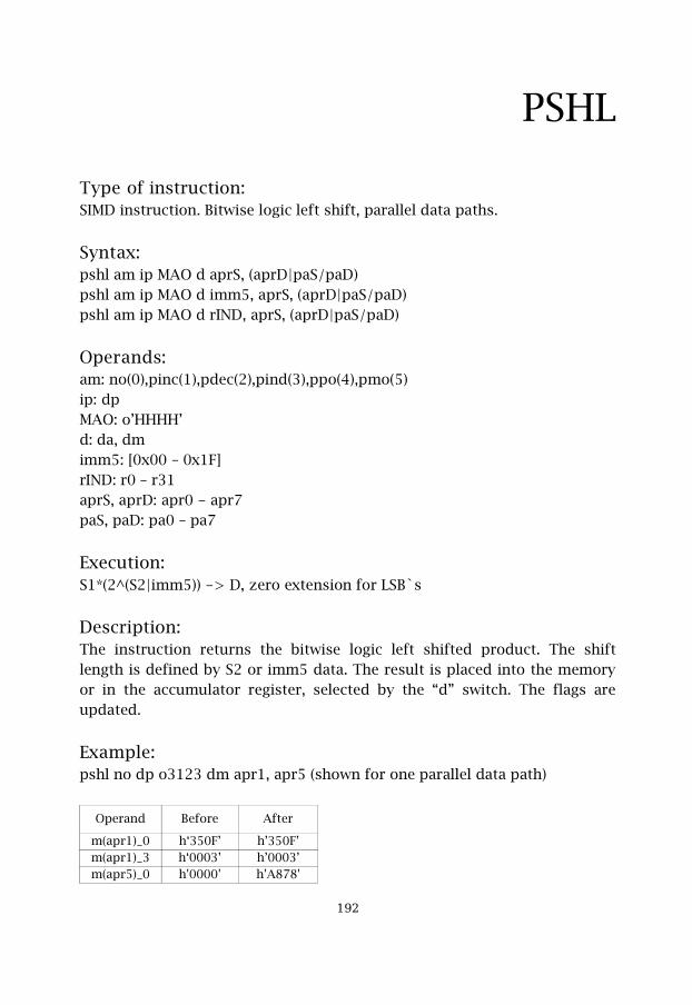
PSHL
Type of instruction:SIMD instruction. Bitwise logic left shift, parallel data paths.
Syntax:pshl am ip MAO d aprS, (aprD|paS/paD)pshl am ip MAO d imm5, aprS, (aprD|paS/paD)pshl am ip MAO d rIND, aprS, (aprD|paS/paD)
Operands: am: no(0),pinc(1),pdec(2),pind(3),ppo(4),pmo(5)ip: dpMAO: o’HHHH’d: da, dmimm5: [0x00 – 0x1F]rIND: r0 – r31aprS, aprD: apr0 - apr7paS, paD: pa0 – pa7
Execution:S1*(2^(S2|imm5)) -> D, zero extension for LSB`s
Description:The instruction returns the bitwise logic left shifted product. The shiftlength is defined by S2 or imm5 data. The result is placed into the memoryor in the accumulator register, selected by the “d” switch. The flags areupdated.
Example:pshl no dp o3123 dm apr1, apr5 (shown for one parallel data path)
Operand Before After
m(apr1)_0 h‘350F’ h’350F’m(apr1)_3 h‘0003’ h’0003’m(apr5)_0 h'0000' h'A878'
��
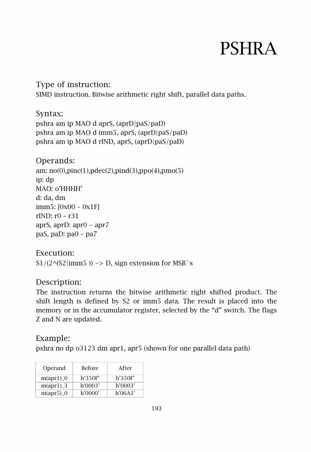
PSHRA
Type of instruction:SIMD instruction. Bitwise arithmetic right shift, parallel data paths.
Syntax:pshra am ip MAO d aprS, (aprD|paS/paD)pshra am ip MAO d imm5, aprS, (aprD|paS/paD)pshra am ip MAO d rIND, aprS, (aprD|paS/paD)
Operands: am: no(0),pinc(1),pdec(2),pind(3),ppo(4),pmo(5)ip: dpMAO: o’HHHH’d: da, dmimm5: [0x00 – 0x1F]rIND: r0 – r31aprS, aprD: apr0 - apr7paS, paD: pa0 – pa7
Execution:S1/(2^(S2|imm5 )) -> D, sign extension for MSB`s
Description:The instruction returns the bitwise arithmetic right shifted product. Theshift length is defined by S2 or imm5 data. The result is placed into thememory or in the accumulator register, selected by the “d” switch. The flagsZ and N are updated.
Example:pshra no dp o3123 dm apr1, apr5 (shown for one parallel data path)
Operand Before After
m(apr1)_0 h‘350F’ h’350F’m(apr1)_3 h‘0003’ h’0003’m(apr5)_0 h'0000' h'06A1'
��
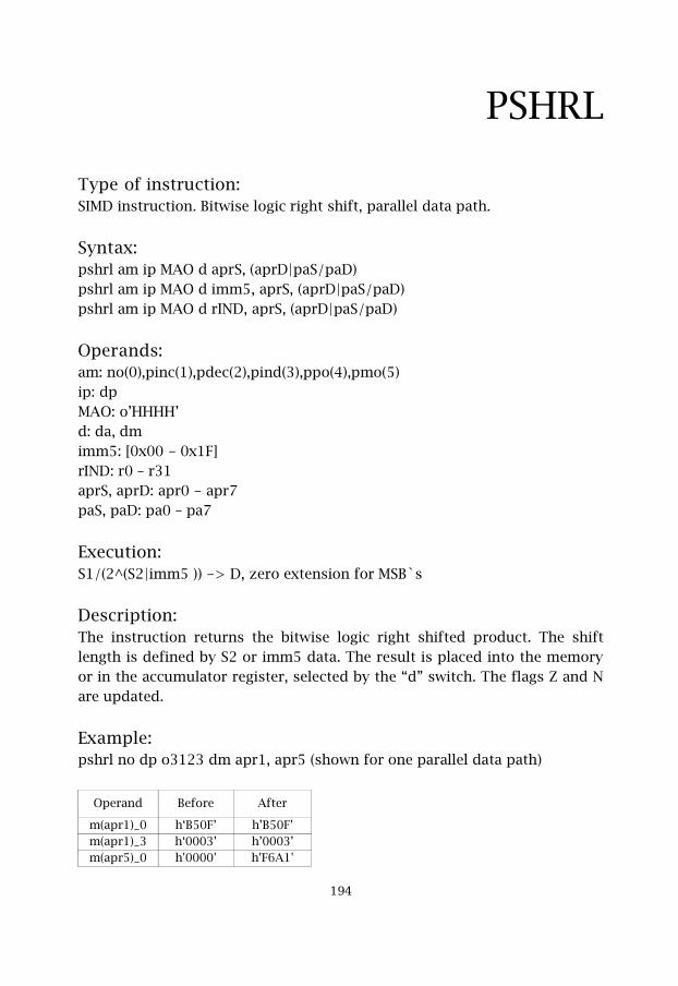
PSHRL
Type of instruction:SIMD instruction. Bitwise logic right shift, parallel data path.
Syntax:pshrl am ip MAO d aprS, (aprD|paS/paD)pshrl am ip MAO d imm5, aprS, (aprD|paS/paD)pshrl am ip MAO d rIND, aprS, (aprD|paS/paD)
Operands: am: no(0),pinc(1),pdec(2),pind(3),ppo(4),pmo(5)ip: dpMAO: o’HHHH’d: da, dmimm5: [0x00 - 0x1F]rIND: r0 – r31aprS, aprD: apr0 - apr7paS, paD: pa0 – pa7
Execution:S1/(2^(S2|imm5 )) -> D, zero extension for MSB`s
Description:The instruction returns the bitwise logic right shifted product. The shiftlength is defined by S2 or imm5 data. The result is placed into the memoryor in the accumulator register, selected by the “d” switch. The flags Z and Nare updated.
Example:pshrl no dp o3123 dm apr1, apr5 (shown for one parallel data path)
Operand Before After
m(apr1)_0 h‘B50F’ h’B50F’m(apr1)_3 h‘0003’ h’0003’m(apr5)_0 h'0000' h'F6A1'
��
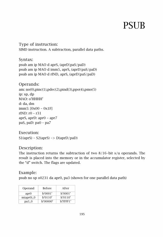
PSUB
Type of instruction:SIMD instruction. A subtraction, parallel data paths.
Syntax:psub am ip MAO d aprS, (aprD|paS/paD)psub am ip MAO d imm5, aprS, (aprD|paS/paD)psub am ip MAO d rIND, aprS, (aprD|paS/paD)
Operands: am: no(0),pinc(1),pdec(2),pind(3),ppo(4),pmo(5)ip: sp, dpMAO: o’HHHH’d: da, dmimm5: [0x00 - 0x1F]rIND: r0 – r31aprS, aprD: apr0 - apr7paS, paD: pa0 – pa7
Execution:S1(aprS) - S2(aprS) -> D(aprD/paD)
Description:The instruction returns the subtraction of two 8/16-bit s/u operands. Theresult is placed into the memory or in the accumulator register, selected bythe “d” switch. The flags are updated.
Example:psub no sp o0231 da apr0, pa3 (shown for one parallel data path)
Operand Before After
apr0 h‘0001’ h’0001’m(apr0)_0 h’0110’ h’0110’
pa3_0 h’00000’ h’FFFF1’
��
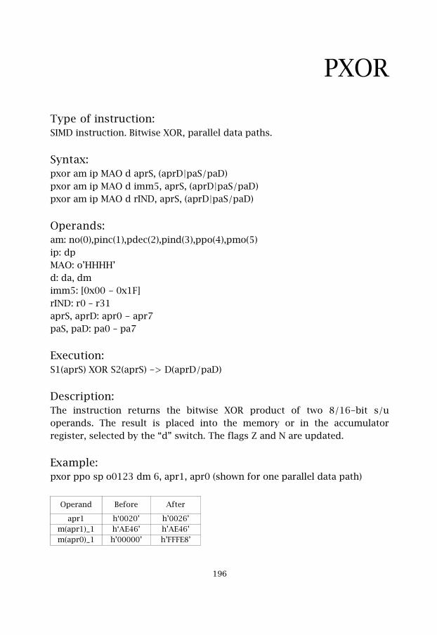
PXOR
Type of instruction:SIMD instruction. Bitwise XOR, parallel data paths.
Syntax:pxor am ip MAO d aprS, (aprD|paS/paD)pxor am ip MAO d imm5, aprS, (aprD|paS/paD)pxor am ip MAO d rIND, aprS, (aprD|paS/paD)
Operands: am: no(0),pinc(1),pdec(2),pind(3),ppo(4),pmo(5)ip: dpMAO: o’HHHH’d: da, dmimm5: [0x00 - 0x1F]rIND: r0 – r31aprS, aprD: apr0 - apr7paS, paD: pa0 – pa7
Execution:S1(aprS) XOR S2(aprS) -> D(aprD/paD)
Description:The instruction returns the bitwise XOR product of two 8/16-bit s/uoperands. The result is placed into the memory or in the accumulatorregister, selected by the “d” switch. The flags Z and N are updated.
Example:pxor ppo sp o0123 dm 6, apr1, apr0 (shown for one parallel data path)
Operand Before After
apr1 h‘0020’ h’0026’m(apr1)_1 h‘AE46’ h’AE46’m(apr0)_1 h’00000’ h’FFFE8’
��
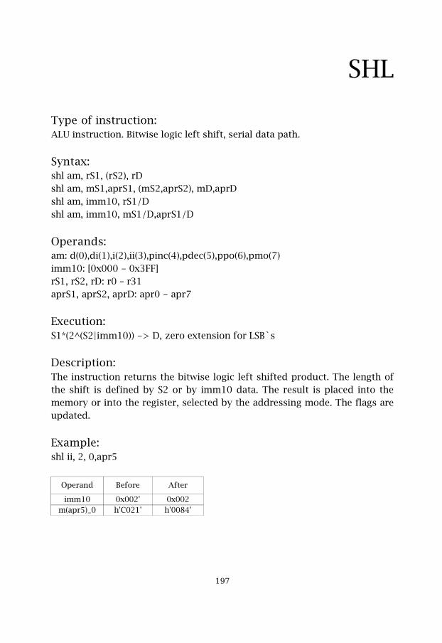
SHL
Type of instruction:ALU instruction. Bitwise logic left shift, serial data path.
Syntax:shl am, rS1, (rS2), rDshl am, mS1,aprS1, (mS2,aprS2), mD,aprDshl am, imm10, rS1/Dshl am, imm10, mS1/D,aprS1/D
Operands: am: d(0),di(1),i(2),ii(3),pinc(4),pdec(5),ppo(6),pmo(7)imm10: [0x000 - 0x3FF]rS1, rS2, rD: r0 – r31aprS1, aprS2, aprD: apr0 - apr7
Execution:S1*(2^(S2|imm10)) -> D, zero extension for LSB`s
Description:The instruction returns the bitwise logic left shifted product. The length ofthe shift is defined by S2 or by imm10 data. The result is placed into thememory or into the register, selected by the addressing mode. The flags areupdated.
Example:shl ii, 2, 0,apr5
Operand Before After
imm10 0x002' 0x002m(apr5)_0 h'C021' h'0084'
��
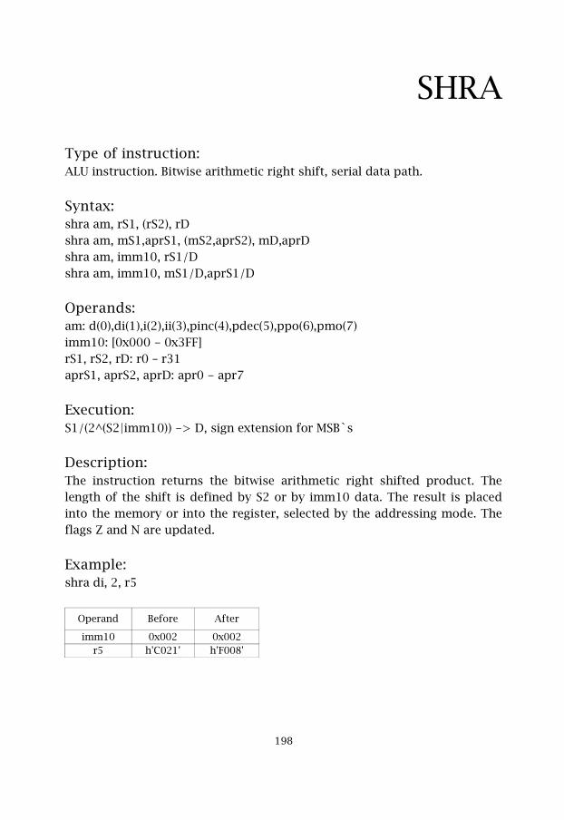
SHRA
Type of instruction:ALU instruction. Bitwise arithmetic right shift, serial data path.
Syntax:shra am, rS1, (rS2), rDshra am, mS1,aprS1, (mS2,aprS2), mD,aprDshra am, imm10, rS1/Dshra am, imm10, mS1/D,aprS1/D
Operands: am: d(0),di(1),i(2),ii(3),pinc(4),pdec(5),ppo(6),pmo(7)imm10: [0x000 - 0x3FF]rS1, rS2, rD: r0 – r31aprS1, aprS2, aprD: apr0 - apr7
Execution:S1/(2^(S2|imm10)) -> D, sign extension for MSB`s
Description:The instruction returns the bitwise arithmetic right shifted product. Thelength of the shift is defined by S2 or by imm10 data. The result is placedinto the memory or into the register, selected by the addressing mode. Theflags Z and N are updated.
Example:shra di, 2, r5
Operand Before After
imm10 0x002 0x002r5 h'C021' h'F008'
��
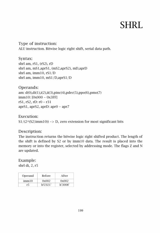
SHRL
Type of instruction:ALU instruction. Bitwise logic right shift, serial data path.
Syntax:shrl am, rS1, (rS2), rDshrl am, mS1,aprS1, (mS2,aprS2), mD,aprDshrl am, imm10, rS1/Dshrl am, imm10, mS1/D,aprS1/D
Operands: am: d(0),di(1),i(2),ii(3),pinc(4),pdec(5),ppo(6),pmo(7)imm10: [0x000 - 0x3FF]rS1, rS2, rD: r0 – r31aprS1, aprS2, aprD: apr0 - apr7
Execution:S1/(2^(S2|imm10)) -> D, zero extension for most significant bits
Description:The instruction returns the bitwise logic right shifted product. The length ofthe shift is defined by S2 or by imm10 data. The result is placed into thememory or into the register, selected by addressing mode. The flags Z and Nare updated.
Example:shrl di, 2, r5
Operand Before After
imm10 0x002 0x002r5 h'C021' h'3008'
�
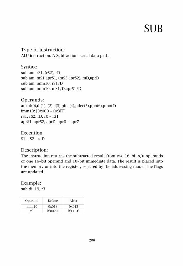
SUB
Type of instruction:ALU instruction. A Subtraction, serial data path.
Syntax:sub am, rS1, (rS2), rDsub am, mS1,aprS1, (mS2,aprS2), mD,aprDsub am, imm10, rS1/Dsub am, imm10, mS1/D,aprS1/D
Operands: am: d(0),di(1),i(2),ii(3),pinc(4),pdec(5),ppo(6),pmo(7)imm10: [0x000 - 0x3FF]rS1, rS2, rD: r0 – r31aprS1, aprS2, aprD: apr0 - apr7
Execution:S1 - S2 -> D
Description:The instruction returns the subtracted result from two 16-bit s/u operandsor one 16-bit operand and 10-bit immediate data. The result is placed intothe memory or into the register, selected by the addressing mode. The flagsare updated.
Example:sub di, 19, r3
Operand Before After
imm10 0x013 0x013r3 h’0020’ h’FFF3’
�((

SUBABS
Type of instruction:ALU instruction. A subtraction of absolute values, serial data path.
Syntax:subabs am, rS1, (rS2), rDsubabs am, mS1,aprS1, (mS2,aprS2), mD,aprDsub am, imm10, rS1/Dsub am, imm10, mS1/D,aprS1/D
Operands: am: d(0),di(1),i(2),ii(3),pinc(4),pdec(5),ppo(6),pmo(7)imm10: [0x000 - 0x3FF]rS1, rS2, rD: r0 – r31aprS1, aprS2, aprD: apr0 - apr7
Execution:abs(S1) – abs(S2) -> D
Description:The instruction returns the subtraction of two absolute 16-bit signedvalues. The result is placed into the memory or into the register, selected bythe addressing mode. The flags are updated.
Example:subabs d, r6, r0, r15
Operand Before After
r6 h’000F’ h’000F’r0 h'FFFE' h'FFFE'r15 h'0000' h'000D'
�(�
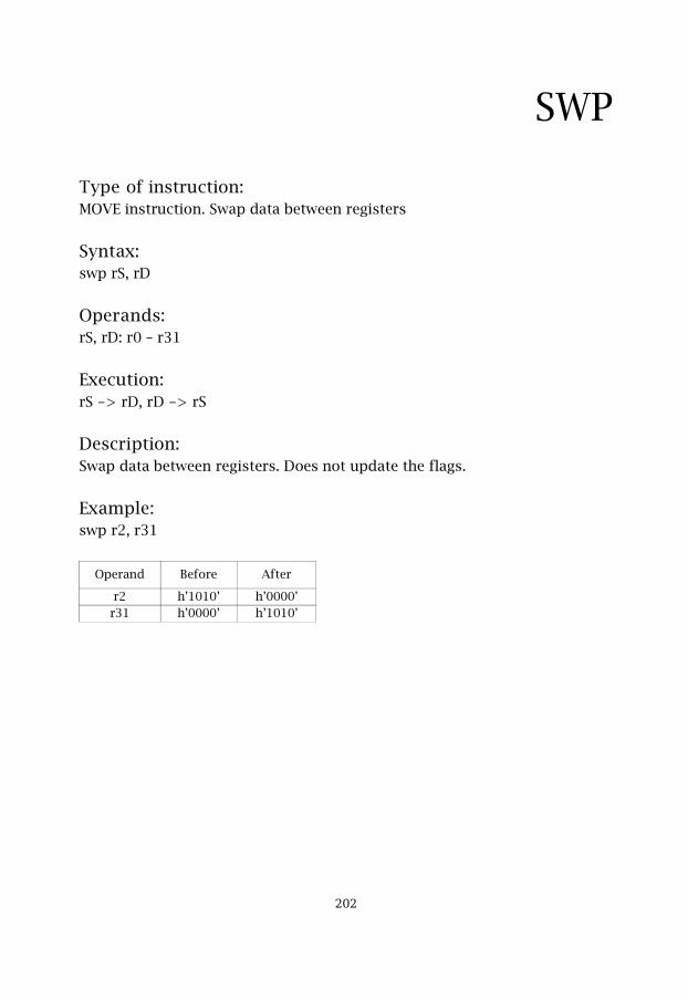
SWP
Type of instruction:MOVE instruction. Swap data between registers
Syntax:swp rS, rD
Operands: rS, rD: r0 – r31
Execution:rS -> rD, rD -> rS
Description:Swap data between registers. Does not update the flags.
Example:swp r2, r31
Operand Before After
r2 h’1010’ h’0000’r31 h’0000’ h’1010’
�(�
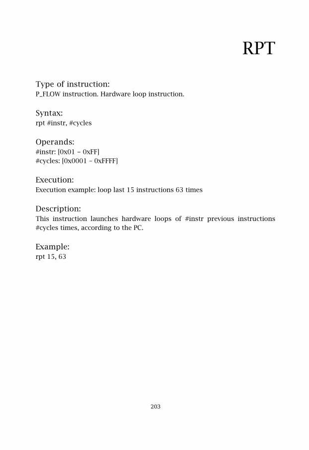
RPT
Type of instruction:P_FLOW instruction. Hardware loop instruction.
Syntax:rpt #instr, #cycles
Operands:#instr: [0x01 - 0xFF]#cycles: [0x0001 – 0xFFFF]
Execution:Execution example: loop last 15 instructions 63 times
Description:This instruction launches hardware loops of #instr previous instructions#cycles times, according to the PC.
Example:rpt 15, 63
�(�
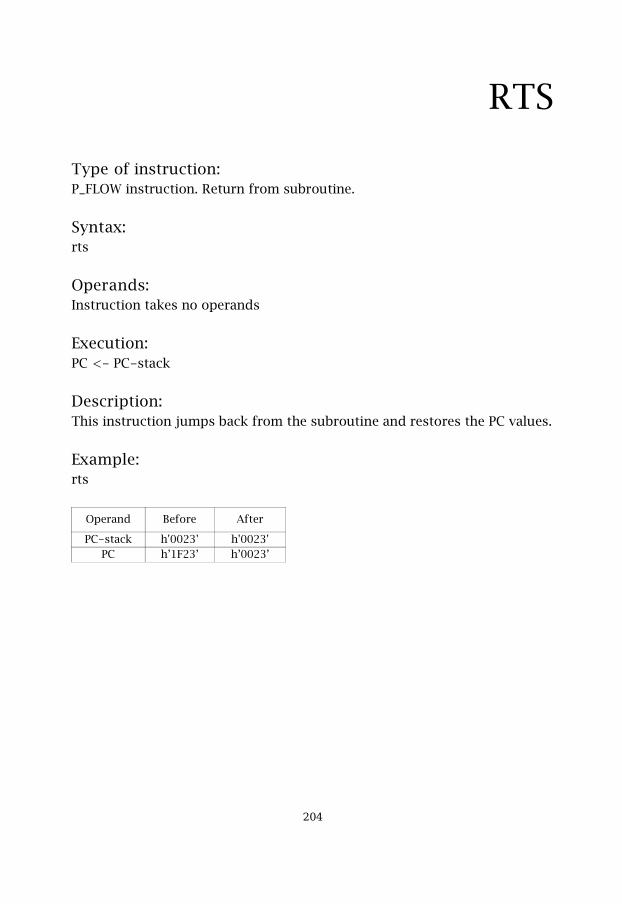
RTS
Type of instruction:P_FLOW instruction. Return from subroutine.
Syntax:rts
Operands:Instruction takes no operands
Execution:PC <- PC-stack
Description:This instruction jumps back from the subroutine and restores the PC values.
Example:rts
Operand Before After
PC-stack h'0023' h'0023'PC h’1F23’ h’0023’
�(�
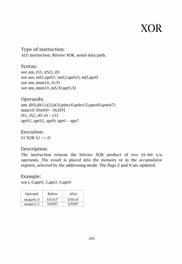
XOR
Type of instruction:ALU instruction. Bitwise XOR, serial data path.
Syntax:xor am, rS1, (rS2), rDxor am, mS1,aprS1, (mS2,aprS2), mD,aprDxor am, imm10, rS/Dxor am, imm10, mS/D,aprS/D
Operands:am: d(0),di(1),i(2),ii(3),pinc(4),pdec(5),ppo(6),pmo(7)imm10: [0x000 – 0x3FF]rS1, rS2, rD: r0 – r31aprS1, aprS2, aprD: apr0 - apr7
Execution:S1 XOR S2 -> D
Description:The instruction returns the bitwise XOR product of two 16-bit s/uoperands. The result is placed into the memory or in the accumulatorregister, selected by the addressing mode. The flags Z and N are updated.
Example:xor i, 0,apr0, 2,apr2, 0,apr0
Operand Before After
m(apr0)_0 h’01E7’ h’FE18’m(apr2)_2 h’FFFF’ h’FFFF’
�(�

�(�
Bibliography
[1] Eric Tell. A Domain Specific DSP Processor, LiTH-ISY-EX-3209,Linköping University, 2001
[2] Dake Liu. Design of Embedded DSP Processors, Department of ElectricalEngineering, Linköping University, 2003
[3] Buyer's Guide to DSP Processors. Berkeley Design Technology Inc., 2001edition
[4] Dake Liu. Introduction to embedded DSP processor design. TSEA80(TSEK15) course lectures, Unit1-13, 2002
[5] Anthony A. Aaby. Compiler construction using Flex and Bison, WallaWalla College, 2003.
[6] John R. Levine, Tony Mason, Doug Brown. Lex & Yacc, 2-nd/updatededition, O'Reilly & Associates, 1992
[7] William Stallings. Computer Organization & Architecture. Design forPerformance, sixth edition, Prentice Hall, 2003
�(�

�(�

På svenska
Detta dokument hålls tillgängligt på Internet – eller dess framtida ersättare – under enlängre tid från publiceringsdatum under förutsättning att inga extra-ordinäraomständigheter uppstår.Tillgång till dokumentet innebär tillstånd för var och en att läsa, ladda ner, skriva utenstaka kopior för enskilt bruk och att använda det oförändrat för ickekommersiellforskning och för undervisning. Överföring av upphovsrätten vid en senare tidpunkt kaninte upphäva detta tillstånd. All annan användning av dokumentet kräver upphovsmannensmedgivande. För att garantera äktheten, säkerheten och tillgängligheten finns det lösningarav teknisk och administrativ art.Upphovsmannens ideella rätt innefattar rätt att bli nämnd som upphovsman i denomfattning som god sed kräver vid användning av dokumentet på ovan beskrivna sätt samtskydd mot att dokumentet ändras eller presenteras i sådan form eller i sådantsammanhang som är kränkande för upphovsmannens litterära eller konstnärliga anseendeeller egenart.För ytterligare information om Linköping University Electronic Press se förlagets hemsidahttp://www.ep.liu.se/
In English
The publishers will keep this document online on the Internet - or its possible replacement- for a considerable time from the date of publication barring exceptional circumstances.The online availability of the document implies a permanent permission for anyone to read,to download, to print out single copies for your own use and to use it unchanged for anynon-commercial research and educational purpose. Subsequent transfers of copyrightcannot revoke this permission. All other uses of the document are conditional on theconsent of the copyright owner. The publisher has taken technical and administrativemeasures to assure authenticity, security and accessibility.According to intellectual property law the author has the right to be mentioned whenhis/her work is accessed as described above and to be protected against infringement.For additional information about the Linköping University Electronic Press and itsprocedures for publication and for assurance of document integrity, please refer to itsWWW home page: http://www.ep.liu.se/
© Vladimir Gnatyuk & Christian Runesson, 2004