Embed Size (px)
Citation preview
SAND REPORT
SAND2003-2954 Unlimited Release Printed September 2003 A Network Architecture for Petaflops Supercomputers
Erik P. DeBenedictis
Prepared by Sandia National Laboratories Albuquerque, New Mexico 87185 and Livermore, California 94550 Sandia is a multiprogram laboratory operated by Sandia Corporation, a Lockheed Martin Company, for the United States Department of Energy under Contract DE-AC04-94AL85000. Approved for public release; further dissemination unlimited.

Issued by Sandia National Laboratories, operated for the United States Department of Energy by Sandia Corporation.
NOTICE: This report was prepared as an account of work sponsored by an agency of the United States Government. Neither the United States Government, nor any agency thereof, nor any of their employees, nor any of their contractors, subcontractors, or their employees, make any warranty, express or implied, or assume any legal liability or responsibility for the accuracy, completeness, or usefulness of any information, apparatus, product, or process disclosed, or represent that its use would not infringe privately owned rights. Reference herein to any specific commercial product, process, or service by trade name, trademark, manufacturer, or otherwise, does not necessarily constitute or imply its endorsement, recommendation, or favoring by the United States Government, any agency thereof, or any of their contractors or subcontractors. The views and opinions expressed herein do not necessarily state or reflect those of the United States Government, any agency thereof, or any of their contractors. Printed in the United States of America. This report has been reproduced directly from the best available copy. Available to DOE and DOE contractors from
U.S. Department of Energy Office of Scientific and Technical Information P.O. Box 62 Oak Ridge, TN 37831 Telephone: (865)576-8401 Facsimile: (865)576-5728 E-Mail: [email protected] Online ordering: http://www.doe.gov/bridge
Available to the public from
U.S. Department of Commerce National Technical Information Service 5285 Port Royal Rd Springfield, VA 22161 Telephone: (800)553-6847 Facsimile: (703)605-6900 E-Mail: [email protected] Online order: http://www.ntis.gov/ordering.htm
2

3
SAND2003-2954 Unlimited Release
Printed August 2003
A Network Architecture for Petaflops Supercomputers
Erik P. DeBenedictis Scalable Computing Systems Sandia National Laboratories
P.O. Box 5800 Albuquerque, New Mexico 87185-1110
Abstract
If we are to build a supercomputer with a speed of 1015 floating operations per second (1 PetaFLOPS), interconnect technology will need to be improved considerably over what it is today. In this report, we explore one possible interconnect design for such a network. The guiding principle in this design is the optimization of all components for the finiteness of the speed of light. To achieve a linear speedup in time over well-tested supercomputers of todays� designs will require scaling up of processor power and bandwidth and scaling down of latency. Latency scaling is the most challenging: it requires a 100 ns user-to-user latency for messages traveling the full diameter of the machine. To meet this constraint requires simultaneously minimizing wire length through 3D packaging, new low-latency electrical signaling mechanisms, extremely fast routers, and new network interfaces. In this report, we outline approaches and implementations that will meet the requirements when implemented as a system. No technology breakthroughs are required.

4
Intentionally Left Blank

5
Contents
Introduction ...........................................................................................................9 Primary Chip Design ...........................................................................................11 Strategies for Low Latency .................................................................................13 Physical Data Transmission................................................................................13 Node Design and 3D Packaging.........................................................................13 Physical Size and Overall Latency......................................................................16 Serviceability.......................................................................................................18 Electrical Issues ..................................................................................................18 Bit Encoding........................................................................................................20 Routing ...............................................................................................................22 Router Chip Architecture.....................................................................................23 Virtual Channels..................................................................................................27 Protocol Engine and NIC ....................................................................................28 Proposed Protocols and User Application Interface............................................29 Error Detection and Recovery.............................................................................30 Deadlock Avoidance in the Event of Faults.........................................................32 Reliability Standard .............................................................................................33 Conclusions ........................................................................................................33 References .........................................................................................................34 Distribution..........................................................................................................35
6
Figures
Figure 1 SOC vs. Discrete���...������������������� 10 Figure 2 ASIC Layout Assuming SOC PIM Implementation���.���.....� 12 Figure 3 Exemplary Layout of Interconnect Across the Chip���...����.. 13 Figure 4 Node Board for Three-Dimensional Packaging.��.�������.. 14 Figure 5 Three Dimensional Packaging��������.����.�..��.. 15 Figure 6 Mapping of 3D Mesh to Physical Structure����������.�.. 15 Figure 7a Water-Cooled (SOC PIM Option)��...������������.. 16 Figure 7b Air-cooled configuration�����...����������....��.. 17 Figure 7c Air-cooled configuration������������.....�����.... 17 Figure 8 Serviceability��...�����..����������������. 18 Figure 9 Dynamic Phase Alignment��.���������.����..��.. 19 Figure 11 Conventional Bit Encoding for DC Balance��...���.��..��.. 20 Figure 12 Bit Encoding for Low Latency while Retaining DC Balance��.....� 22 Figure 13 Router Layout for Fast Straight Ahead Routes..������..��.. 23 Figure 14 Detail of Straight-Ahead Logic��...��������..��..��.. 24 Figure 15 Three Traffic Lanes for Turn Logic��...�����..������. 25 Figure 16 Directional Interface��...�����������...���...��.. 25 Figure 17 Dimensions of Routing Lanes��...�����������..��.. 26 Figure 18 Multiplexing Virtual Channels on a Physical Channel���..�..�.. 27 Figure 19 Dual Virtual Channels and Protocol Handling��...����...��.. 27 Figure 20 Protocol Engine��.������������..�����..��.. 29 Figure 21 2-Hop Error Detection and Recovery��...��������.��.. 31
Tables
Table 1. Basic System Parameters���..��.�������������.. 11 Table 3. Application of Protocols to the Protocol Engine��������...�.. 29
7
Nomenclature
3D..�........................................................................................Three Dimensional ASCI..�............................. Advanced Simulation and Computing (the �I� is silent) ASIC..�.......................................................Application Specific Integrated Circuit CPU..�............................................................................. Central Processing Unit CRC..�.. ...................................................................... Cyclic Reduncancy Check DC..�.. ............................................................................................ Direct Current DIMMs..�.. ................................................................................... Memory Module DOE�.. ...............................................................................Department of Energy DRAM�...........................................................Dynamic Random Access Memory FLOPS..�.. .........................................................Floating Operations Per Second GFLOPS..�................................................... 109 Floating Operations per Second ITRS�.. .......................... International Technology Roadmap for Semiconductors MPI..�.........................................................................Message Passing Interface MPP..�.. .................................................................. Massively Parallel Processor NIC..�.. .............................................................. Network Interface Chip (or Card) PetaFLOPS..�.. .......................................... 1015 Floating Operations Per Second PIM�....................................................................................Processor In Memory RAM..�.. ........................................................................Random Access Memory SNL�.. .....................................................................Sandia National Laboratories SOC�.. ........................................................................................System On Chip

8
Intentionally Left Blank
9
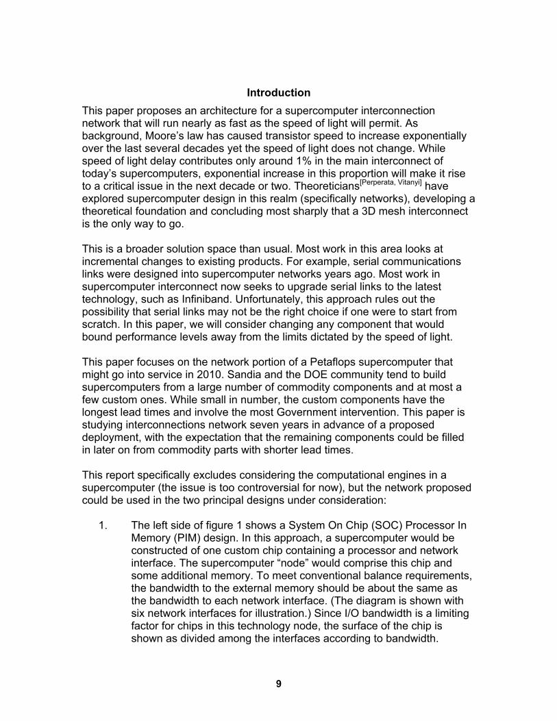
Introduction This paper proposes an architecture for a supercomputer interconnection network that will run nearly as fast as the speed of light will permit. As background, Moore�s law has caused transistor speed to increase exponentially over the last several decades yet the speed of light does not change. While speed of light delay contributes only around 1% in the main interconnect of today�s supercomputers, exponential increase in this proportion will make it rise to a critical issue in the next decade or two. Theoreticians[Perperata, Vitanyi] have explored supercomputer design in this realm (specifically networks), developing a theoretical foundation and concluding most sharply that a 3D mesh interconnect is the only way to go. This is a broader solution space than usual. Most work in this area looks at incremental changes to existing products. For example, serial communications links were designed into supercomputer networks years ago. Most work in supercomputer interconnect now seeks to upgrade serial links to the latest technology, such as Infiniband. Unfortunately, this approach rules out the possibility that serial links may not be the right choice if one were to start from scratch. In this paper, we will consider changing any component that would bound performance levels away from the limits dictated by the speed of light. This paper focuses on the network portion of a Petaflops supercomputer that might go into service in 2010. Sandia and the DOE community tend to build supercomputers from a large number of commodity components and at most a few custom ones. While small in number, the custom components have the longest lead times and involve the most Government intervention. This paper is studying interconnections network seven years in advance of a proposed deployment, with the expectation that the remaining components could be filled in later on from commodity parts with shorter lead times. This report specifically excludes considering the computational engines in a supercomputer (the issue is too controversial for now), but the network proposed could be used in the two principal designs under consideration:
1. The left side of figure 1 shows a System On Chip (SOC) Processor In Memory (PIM) design. In this approach, a supercomputer would be constructed of one custom chip containing a processor and network interface. The supercomputer �node� would comprise this chip and some additional memory. To meet conventional balance requirements, the bandwidth to the external memory should be about the same as the bandwidth to each network interface. (The diagram is shown with six network interfaces for illustration.) Since I/O bandwidth is a limiting factor for chips in this technology node, the surface of the chip is shown as divided among the interfaces according to bandwidth.
10
2. The right side of figure 1 shows the more conventional discrete implementation of a Massively Parallel Processor (MPP) node. In this approach, a conventional microprocessor chip interfaces to a network chip and DRAM. To meet conventional balance requirements, the network interface chip�s interface to the microprocessor (and DRAM) should be about the same as the bandwidth to each network interface. This creates the same bandwidth and pin allocation as the SOC PIM approach.
In our view, both the SOC PIM and discrete approaches are candidates for the 2010 time frame (the SOC PIM probably yielding a more efficient design but with higher development costs). We will �hedge our bets� by proceeding in this report in a manner largely compatible with both approaches. However, we will use the SOC PIM for illustration. Other issues addressed in this report include:
• A compact but serviceable 3D physical design compatible with both water and air cooling
CPU
I/O Bus
Microprocessor
Memory Bus
DRAM
DRAM
DRAM
-X +X
-Y +Z
+Y -Z
-X +X
-Y +Z
+Y -Z
System On Chip (SOC) Processor In Memory (PIM)
Discrete Component Design Cluster/ASCI Red
Figure 1: SOC vs. Discrete
11
• Dynamic Phase Alignment as a low latency alternative to clock synchronization
• A DC balancing method with zero latency
• Deadlock free routing
• Router optimized to the most common route � straight ahead routing
• A router design with three-lanes but with the performance of a full
crossbar
• Virtual channels and a generalized �protocol engine� for message processing in a couple clock cycles
• Support for both shared memory and message passing communications
semantics
• Error detection and recovery capable of mitigating a failing router chip The assumed parameters for the Petaflops supercomputer are given in the table below: Physical Size 5� x 7� x 12� Nodes 10368 @ 100 Gflops Topology 3D mesh 27 x 16 x 24 Clock rate 10 GHz External signaling rate 40 GHz Cross-machine latency 100 ns Link bandwidth @ 4 bytes/flop 400 GBytes/sec Wires per link per direction 160 Interconnect pins/chip 1920
Table 1: Basic System Parameters
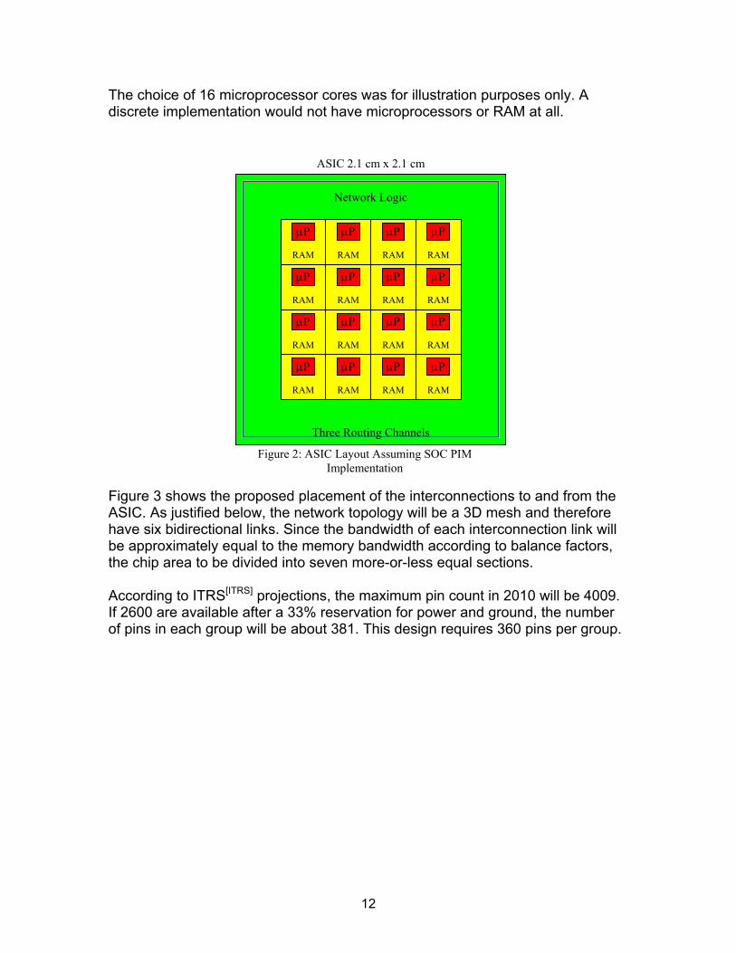
Primary Chip Design Each node will consist of a main Application Specific Integrated Circuit (ASIC) and extra memory. For a SOC PIM implementation, the approximate floor plan of the ASIC is shown in figure 2 and comprises a network interface around the periphery with a central section comprised of some number of microprocessor cores (µP) with associated memory.
12
The choice of 16 microprocessor cores was for illustration purposes only. A discrete implementation would not have microprocessors or RAM at all.
Figure 3 shows the proposed placement of the interconnections to and from the ASIC. As justified below, the network topology will be a 3D mesh and therefore have six bidirectional links. Since the bandwidth of each interconnection link will be approximately equal to the memory bandwidth according to balance factors, the chip area to be divided into seven more-or-less equal sections. According to ITRS[ITRS] projections, the maximum pin count in 2010 will be 4009. If 2600 are available after a 33% reservation for power and ground, the number of pins in each group will be about 381. This design requires 360 pins per group.
ASIC 2.1 cm x 2.1 cm
µP
RAM
µP
RAM
µP
RAM
µP
RAM
µP
RAM
µP
RAM
µP
RAM
µP
RAM
µP
RAM
µP
RAM
µP
RAM
µP
RAM
µP
RAM
µP
RAM
µP
RAM
µP
RAM
Network Logic
Three Routing Channels
Figure 2: ASIC Layout Assuming SOC PIM Implementation
13
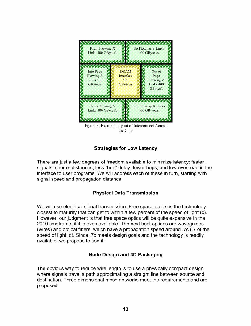
Strategies for Low Latency
There are just a few degrees of freedom available to minimize latency: faster signals, shorter distances, less �hop� delay, fewer hops, and low overhead in the interface to user programs. We will address each of these in turn, starting with signal speed and propagation distance.
Physical Data Transmission We will use electrical signal transmission. Free space optics is the technology closest to maturity that can get to within a few percent of the speed of light (c). However, our judgment is that free space optics will be quite expensive in the 2010 timeframe, if it is even available. The next best options are waveguides (wires) and optical fibers, which have a propagation speed around .7c (.7 of the speed of light, c). Since .7c meets design goals and the technology is readily available, we propose to use it.
Node Design and 3D Packaging The obvious way to reduce wire length is to use a physically compact design where signals travel a path approximating a straight line between source and destination. Three dimensional mesh networks meet the requirements and are proposed.
DRAM Interface
400 GBytes/s
Right Flowing X Links 400 GBytes/s
Left Flowing X Links 400 GBytes/s
Up Flowing Y Links 400 GBytes/s
Down Flowing Y Links 400 GBytes/s
Into Page Flowing Z Links 400 GBytes/s
Out of Page
Flowing Z Links 400 GBytes/s
Figure 3: Example Layout of Interconnect Across the Chip
14
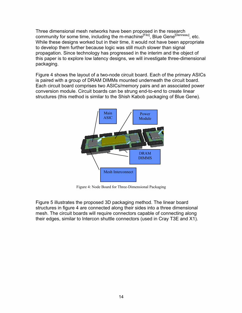
Three dimensional mesh networks have been proposed in the research community for some time, including the m-machine[Filo], Blue Gene[Denneau], etc. While these designs worked but in their time, it would not have been appropriate to develop them further because logic was still much slower than signal propagation. Since technology has progressed in the interim and the object of this paper is to explore low latency designs, we will investigate three-dimensional packaging. Figure 4 shows the layout of a two-node circuit board. Each of the primary ASICs is paired with a group of DRAM DIMMs mounted underneath the circuit board. Each circuit board comprises two ASICs/memory pairs and an associated power conversion module. Circuit boards can be strung end-to-end to create linear structures (this method is similar to the Shish Kabob packaging of Blue Gene).
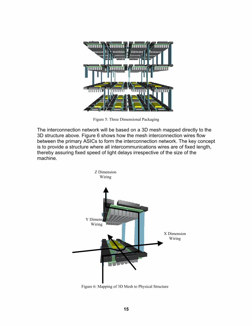
Figure 5 illustrates the proposed 3D packaging method. The linear board structures in figure 4 are connected along their sides into a three dimensional mesh. The circuit boards will require connectors capable of connecting along their edges, similar to Intercon shuttle connectors (used in Cray T3E and X1).
MainASIC
Power Module
DRAM DIMMS
Mesh Interconnect
Figure 4: Node Board for Three-Dimensional Packaging
15
The interconnection network will be based on a 3D mesh mapped directly to the 3D structure above. Figure 6 shows how the mesh interconnection wires flow between the primary ASICs to form the interconnection network. The key concept is to provide a structure where all intercommunications wires are of fixed length, thereby assuring fixed speed of light delays irrespective of the size of the machine.
Figure 5: Three Dimensional Packaging
X Dimension Wiring
Z Dimension Wiring
Y Dimension Wiring
Figure 6: Mapping of 3D Mesh to Physical Structure
16
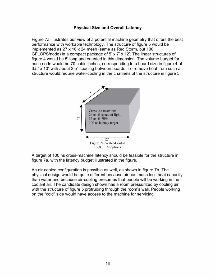
Physical Size and Overall Latency Figure 7a illustrates our view of a potential machine geometry that offers the best performance with workable technology. The structure of figure 5 would be implemented as 27 x 16 x 24 mesh (same as Red Storm, but 100 GFLOPS/node) in a compact package of 5� x 7� x 12�. The linear structures of figure 4 would be 5� long and oriented in this dimension. The volume budget for each node would be 70 cubic inches, corresponding to a board size in figure 4 of 3.5� x 10� with about 3.5� spacing between boards. To remove heat from such a structure would require water-cooling in the channels of the structure in figure 5.
A target of 100 ns cross-machine latency should be feasible for the structure in figure 7a, with the latency budget illustrated in the figure. An air-cooled configuration is possible as well, as shown in figure 7b. The physical design would be quite different because air has much less heat capacity than water and because air-cooling presumes that people will be working in the coolant air. The candidate design shown has a room pressurized by cooling air with the structure of figure 5 protruding through the room�s wall. People working on the �cold� side would have access to the machine for servicing.
12’
7’
5’
Cross the machine:24 ns @ speed of light 35 ns @ 70% 100 ns latency target
Figure 7a: Water-Cooled (SOC PIM option)

17
With a full-machine power dissipation of 1.5 MW, the configuration in figure 7b and 7c moving air at 20 fps would heat air from 70° F to 97° F (15° C).
Figure 7c: Air-cooled Configuration
Window to room with power supplies and heat exhaust. A pressure differential of about 2� H2O will supply sufficient airflow to cool the machine.
Figure 7b: Air-cooled configuration
18
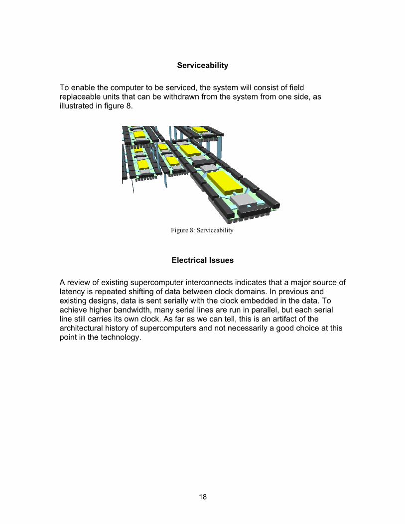
Serviceability
To enable the computer to be serviced, the system will consist of field replaceable units that can be withdrawn from the system from one side, as illustrated in figure 8.
Electrical Issues
A review of existing supercomputer interconnects indicates that a major source of latency is repeated shifting of data between clock domains. In previous and existing designs, data is sent serially with the clock embedded in the data. To achieve higher bandwidth, many serial lines are run in parallel, but each serial line still carries its own clock. As far as we can tell, this is an artifact of the architectural history of supercomputers and not necessarily a good choice at this point in the technology.
Figure 8: Serviceability
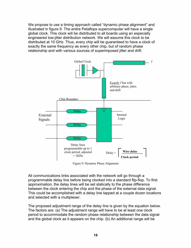
19
We propose to use a timing approach called �dynamic phase alignment� and illustrated in figure 9. The entire Petaflops supercomputer will have a single global clock. This clock will be distributed to all boards using an especially engineered low-jitter distribution network. We will assume this clock to be distributed at 10 GHz. Thus, every chip will be guaranteed to have a clock of exactly the same frequency as every other chip, but of random phase relationship and with various sources of superimposed jitter and drift.
All communications links associated with the network will go through a programmable delay line before being clocked into a standard flip-flop. To first approximation, the delay lines will be set statically to the phase difference between the clock entering the chip and the phase of the external data signal. This could be accomplished with a delay line tapped at a couple dozen locations and selected with a multiplexer. The proposed adjustment range of the delay line is given by the equation below. The factors are: (a) The adjustment range will have to be at least one clock period to accommodate the random phase relationship between the data signal and the global clock as it appears on the chip. (b) An additional range will be
f
Exactly f but with arbitrary phase, jitter, and drift
Internal Logic
Delay lines programmable up to 1 clock period, adjusted
< 1KHz
Chip Boundary
Global Clock
External Signals
Wire delay
Clock period ⎡ ⎤ Delay =
Delay
Delay
Delay
Figure 9: Dynamic Phase Alignment

20
needed to accommodate differing wire lengths for bits in data busses. (3) Additional range to accommodate periodic adjustment to jitter.
Trange = Tclk + T∆wire + Tjitter + Tmargin where Trange is the adjustment range Tclk is the system clock period (100 ps) T∆wire is the transit time difference in data wires Tjitter is other sources of jitter Tmargin is a timing margin
This form of clock latency adjustment will add at most one clock period to whatever the delay is in the wire. Completely static settings of the delay lines are unlikely to work at the highest frequencies due to jitter. Specifically, the relative phase between the clock and data at any chip will vary due to factors like:
1. Jitter caused by power supply noise 2. Drift caused by cables expanding and contracting due to temperature
or changes in dielectric constant in transmission lines causing changes in propagation velocity
3. Intersymbol jitter on data lines (clock distribution does not have this
jitter because there are no symbols)
Jitter and drift in sources 1 & 2 could be accommodated by logic that adjusts the delay lines by monitoring the placement of transitions at a relatively slow rate (<1KHz). Jitter source 3 will need to be minimized, but may define the limits of this method.
Bit Encoding Figure 11 shows the conventional method of assuring constant DC levels on high speed lines.
The conventional method has unnecessary latency. Specifically, the method is designed with a 10-bit DC-balanced code word transmitted serially over each
10 bit shift register
8 bit parallel register
Look at first bit after 11 clock
cycles
10-8 Converter
Figure 11: Conventional Bit Encoding for DC Balance
21
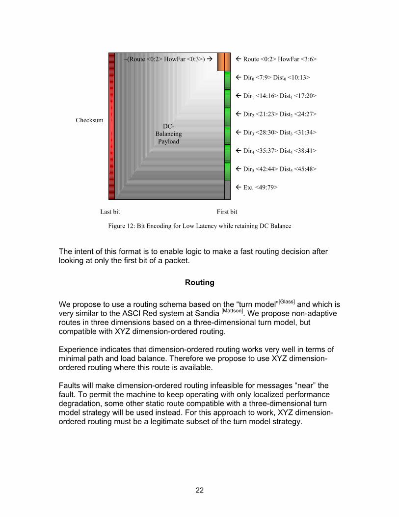
data line. The code words are shifted into a register over a period of 10 clocks, after which the code word in translated in parallel to a non-DC-balanced byte. The entire process has a latency of 11 clock cycles between the time the first bit arrives on the wire and when the logic can make its first decision based on its contents. We propose a method with significantly lower latency. The idea behind bit encoding for DC balance is to pick code words with the same number of 1s and 0s. There is no particular reason why the first, second, third, or any particular bit, needs to be constrained to achieve this balance. We therefore propose to use a code word where the first bit of each serial stream is a plain data bit. This shifts the DC balance constraint to the second and later bits. We also propose a method where the router can alter data in the message while still retaining DC balance. To avoid routing tables, each message will contain the routing path (source based routing). However, each router will need to know where it is in the route. While there are several ways to do this, we propose that each message have a 7-bit field containing the �state� of the message along the route. As the message flows through each router, this field gets altered. However, this will change the DC balance of each bit line switched. To compensate, we propose that the state field be immediately followed by its complement. The router is therefore free to modify the state field as it chooses as long as it takes responsibility for injecting the complement in the subsequent bits. The proposed packet format is shown below. The interconnect consists of 80 bit parallel busses, thus defining the packet width. The 80 bits comprising the first bit on each signal contain as the information necessary to route the packet, as well as some data. The route is defined by up to six segments each of up to 16 �hops.� Dirn and Distn give the direction and distance of the n�th hop. To enable to router to know how far through the route a message has gotten, a state field is included comprised of an indication of which of the routes (Route<0:2>) is currently being traversed and how many �hops� down the route the message had already traveled as it entered the router (HowFar<3:6>). The state field is followed by its complement.
22
The intent of this format is to enable logic to make a fast routing decision after looking at only the first bit of a packet.
Routing We propose to use a routing schema based on the �turn model�[Glass] and which is very similar to the ASCI Red system at Sandia [Mattson]. We propose non-adaptive routes in three dimensions based on a three-dimensional turn model, but compatible with XYZ dimension-ordered routing. Experience indicates that dimension-ordered routing works very well in terms of minimal path and load balance. Therefore we propose to use XYZ dimension-ordered routing where this route is available. Faults will make dimension-ordered routing infeasible for messages �near� the fault. To permit the machine to keep operating with only localized performance degradation, some other static route compatible with a three-dimensional turn model strategy will be used instead. For this approach to work, XYZ dimension-ordered routing must be a legitimate subset of the turn model strategy.
! Dir0 <7:9> Dist0 <10:13>
! Dir1 <14:16> Dist1 <17:20>
! Dir2 <21:23> Dist2 <24:27>
! Dir3 <28:30> Dist3 <31:34>
! Dir4 <35:37> Dist4 <38:41>
! Dir5 <42:44> Dist5 <45:48>
! Route <0:2> HowFar <3:6> ~(Route <0:2> HowFar <0:3>) "
! Etc. <49:79>
DC-Balancing Payload
Checksum
First bit Last bit
Figure 12: Bit Encoding for Low Latency while retaining DC Balance

23
Router Chip Architecture We propose to lay out the router to provide best performance for the most common case, filling in the rest of the design in a second stage. Most of the time messages will go through the router in a straight line, changing direction only a few times in an entire route. The router design in figure 13 has a fast and direct pathway for messages continuing straight ahead.
The router chip will have physically compact cut-through logic to handle data flows in each of the 6 directions (only 4 directions shown above). For example, the cut-through block highlighted in the diagram above handles messages arriving from the left and continuing to the right. The purpose of each such cut-through block will be to make a one-cycle decision as to whether an incoming message can be �cut through� to the output link right away or routed to more turn and queuing logic elsewhere on the chip. This should be feasible in a short time because the only information needed will be the first address field and a flag indicating that the output buffer is currently available.
Turn Logic
This logic block optimized for
messages flowing right with no turns
Figure 13: 2D Router Layout for Fast Straight Ahead Routes
Router Chip
24
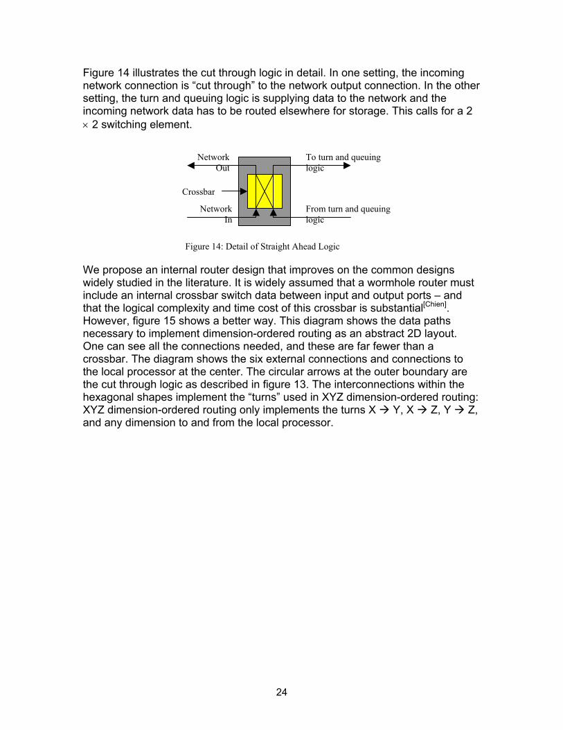
Figure 14 illustrates the cut through logic in detail. In one setting, the incoming network connection is �cut through� to the network output connection. In the other setting, the turn and queuing logic is supplying data to the network and the incoming network data has to be routed elsewhere for storage. This calls for a 2 × 2 switching element.
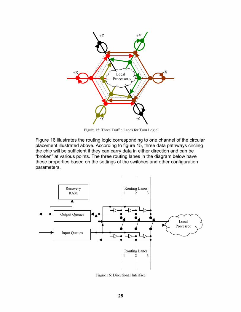
We propose an internal router design that improves on the common designs widely studied in the literature. It is widely assumed that a wormhole router must include an internal crossbar switch data between input and output ports � and that the logical complexity and time cost of this crossbar is substantial[Chien]. However, figure 15 shows a better way. This diagram shows the data paths necessary to implement dimension-ordered routing as an abstract 2D layout. One can see all the connections needed, and these are far fewer than a crossbar. The diagram shows the six external connections and connections to the local processor at the center. The circular arrows at the outer boundary are the cut through logic as described in figure 13. The interconnections within the hexagonal shapes implement the �turns� used in XYZ dimension-ordered routing: XYZ dimension-ordered routing only implements the turns X " Y, X " Z, Y " Z, and any dimension to and from the local processor.
NetworkIn
NetworkOut
Crossbar
To turn and queuing logic
From turn and queuing logic
Figure 14: Detail of Straight Ahead Logic
25
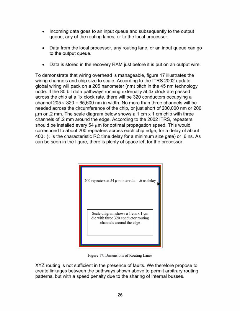
Figure 16 illustrates the routing logic corresponding to one channel of the circular placement illustrated above. According to figure 15, three data pathways circling the chip will be sufficient if they can carry data in either direction and can be �broken� at various points. The three routing lanes in the diagram below have these properties based on the settings of the switches and other configuration parameters.
-X +X
+Z
-Z
+Y
-Y
Local Processor
Figure 15: Three Traffic Lanes for Turn Logic
Output Queues
Input Queues
Recovery RAM
Local Processor
Routing Lanes 1 2 3
Routing Lanes 1 2 3
Figure 16: Directional Interface
26
• Incoming data goes to an input queue and subsequently to the output queue, any of the routing lanes, or to the local processor.
• Data from the local processor, any routing lane, or an input queue can go
to the output queue.
• Data is stored in the recovery RAM just before it is put on an output wire. To demonstrate that wiring overhead is manageable, figure 17 illustrates the wiring channels and chip size to scale. According to the ITRS 2002 update, global wiring will pack on a 205 nanometer (nm) pitch in the 45 nm technology node. If the 80 bit data pathways running externally at 4x clock are passed across the chip at a 1x clock rate, there will be 320 conductors occupying a channel 205 × 320 = 65,600 nm in width. No more than three channels will be needed across the circumference of the chip, or just short of 200,000 nm or 200 µm or .2 mm. The scale diagram below shows a 1 cm x 1 cm chip with three channels of .2 mm around the edge. According to the 2002 ITRS, repeaters should be installed every 54 µm for optimal propagation speed. This would correspond to about 200 repeaters across each chip edge, for a delay of about 400τ (τ is the characteristic RC time delay for a minimum size gate) or .6 ns. As can be seen in the figure, there is plenty of space left for the processor.
XYZ routing is not sufficient in the presence of faults. We therefore propose to create linkages between the pathways shown above to permit arbitrary routing patterns, but with a speed penalty due to the sharing of internal busses.
200 repeaters at 54 µm intervals � .6 ns delay
Scale diagram shows a 1 cm x 1 cm die with three 320 conductor routing
channels around the edge
Figure 17: Dimensions of Routing Lanes
27
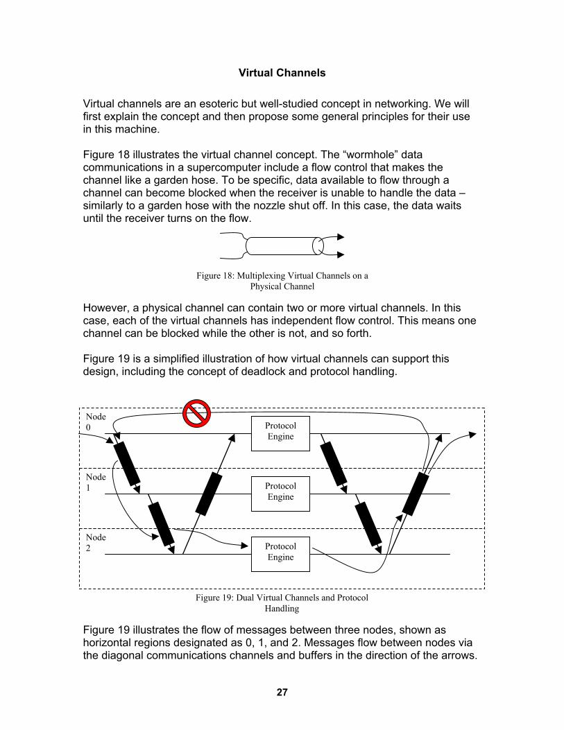
Virtual Channels Virtual channels are an esoteric but well-studied concept in networking. We will first explain the concept and then propose some general principles for their use in this machine. Figure 18 illustrates the virtual channel concept. The �wormhole� data communications in a supercomputer include a flow control that makes the channel like a garden hose. To be specific, data available to flow through a channel can become blocked when the receiver is unable to handle the data � similarly to a garden hose with the nozzle shut off. In this case, the data waits until the receiver turns on the flow.
However, a physical channel can contain two or more virtual channels. In this case, each of the virtual channels has independent flow control. This means one channel can be blocked while the other is not, and so forth. Figure 19 is a simplified illustration of how virtual channels can support this design, including the concept of deadlock and protocol handling.
Figure 19 illustrates the flow of messages between three nodes, shown as horizontal regions designated as 0, 1, and 2. Messages flow between nodes via the diagonal communications channels and buffers in the direction of the arrows.
Figure 18: Multiplexing Virtual Channels on a Physical Channel
Protocol Engine
Protocol Engine
Protocol Engine
Node 0
Node 1
Node 2
Figure 19: Dual Virtual Channels and Protocol Handling

28
Deadlock could occur if there were a circular dependency in the data flows between buffers, such as the one illustrated by the wavy line (including the ! symbol on the illegal pathway that would be required to complete the cycle). We have drawn the diagram where all diagonal buffers point rightward. The rightward motion assures that figure 19 is an acyclic graph and as a result, a machine built this way would never incur deadlock. The proposed network for this machine will not have deadlock-enabling cycles due to the nature of the turns permitted in table 2. Thus one could in principle draw a diagram like figure 19 for this machine. However, the diagram would have over a quarter million buffers and would not be practical to draw. To assure proper operation at speed, we propose special support in the network for the protocols that underlie the operation of supercomputers, such as shared memory and message passing. Both these protocols have a step where a message is received (either a shared memory address or a message data packet) and is followed immediately with a response (memory data return or data acknowledgement). Without virtual channels, the immediate response creates a leftward flowing buffer dependency, a cycle, and the possibility of deadlock. The virtual channel in figure 19 permits efficient protocol handling while avoiding deadlock. The strategy is to put the initial messages in each pair on one virtual channel and the response messages on the other virtual channel. As one can see from figure 19, the entire flow of the request through the first virtual network, the generation of the response, and the flow of the response through the second virtual network creates leftward flowing buffer dependencies through the entire diagram. We are therefore proposing two sets of virtual channels for requests and responses in a request-response protocol. This design is well known for distributed shared memory systems and there is extensive information on its performance. However, this approach is not widely used in message-based systems.
Protocol Engine and NIC To meet speed requirements while maintaining sufficient functionality, the network interface will need substantial improvement over those in common use today. Today�s distributed shared memory systems (such as X1) are engineered for low latency and may serve as a model in this respect. However, today�s software stacks for MPI, Portals, and other message passing protocols have functionality enhancements that permit them to scale to enormous sizes. We therefore propose to merge these two approaches into a protocol engine that can achieve both low latency and broad functionality.
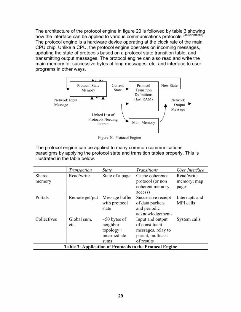
29
The architecture of the protocol engine in figure 20 is followed by table 3 showing how the interface can be applied to various communications protocols.[DeBenedictis] The protocol engine is a hardware device operating at the clock rate of the main CPU chip. Unlike a CPU, the protocol engine operates on incoming messages, updating the state of protocols based on a protocol state transition table, and transmitting output messages. The protocol engine can also read and write the main memory for successive bytes of long messages, etc. and interface to user programs in other ways.
The protocol engine can be applied to many common communications paradigms by applying the protocol state and transition tables properly. This is illustrated in the table below. Transaction State Transitions User Interface Shared memory
Read/write State of a page Cache coherence protocol (or non coherent memory access)
Read/write memory; map pages
Portals Remote get/put Message buffer with protocol state
Successive receipt of data packets and periodic acknowledgements
Interrupts and MPI calls
Collectives Global sum, etc.
~50 bytes of neighbor topology + intermediate sums
Input and output of constituent messages, relay to parent, multicast of results
System calls
Table 3: Application of Protocols to the Protocol Engine
Protocol State Memory
Protocol Transition Definitions(fast RAM)
Current State
New State
Network Input Message
NetworkOutput
MessageLinked List of
Protocols Needing Output Main Memory
Figure 20: Protocol Engine
30
Proposed Protocols and User Application Interface
The design of the network interface is beyond the scope of this report. However, the type of protocol engine described above should be able to support all of the widely-used communications paradigms, including:
1. MPI support: A variety of primitives to send/receive a message to a remote buffer pool in a sufficient set of variants to support MPI�s synchronization modes.
2. Shared Memory: Read and write remote memory with optional coherence. Will use two virtual channels for address and reply.
3. Collectives: Hardware-based protocols to synchronize over a subset of the machine directly in the network fabric.
4. Locks and semaphores. 5. Multiphase commit. 6. The functions above to be operable with a programmable channel capable
of sequencing a number of operations on sequential, strided, or indirect addresses. This programmable channel is to be fast enough to drive the network at full speed and without incurring latency beyond what is necessary for access to the channel command structure (in other words, this is not to be a microprocessor).
7. A programmable NIC for higher-level operations, such as boundary exchange support, TCP/IP, etc.
Error Detection and Recovery
An ASCI-size supercomputer must continue to run even when a chip fails. The number of parts is large enough that some part will fail often � every few days to every week or so. The degree of failure tolerance generally accepted by ASCI is for the application actually using the failing component to abort, but for the overall supercomputer and all other applications to continue running. In addition, the supercomputer should support hot swapping of components so that the failed component can be replaced and the machine returned to fully operational status. We propose an improved method of achieving high reliability, including tolerance of hard and soft errors. The two methods that serve as the base for our improvements are:
1. Most systems today have end-to-end error detection with retransmission for recovery. While this method is proven, the resulting protocols are error prone and introduce overhead that cuts performance even in the absence of faults.
2. Many systems today also employ a local error detection and recovery. However, a local method is vulnerable to hard failure of a router chip. In a local method, router chips store messages in internal memories. Hard failure of a router chip causes loss of some messages in transit.

31
We propose a two-hop error detection and recovery method as illustrated in figure 21. In this method, each router chip (labeled �self�) retains a copy of all transmitted messages (messages are green; copies are red) until the message has been successfully received two hops away � its neighbor�s neighbor.
Figure 21 illustrates the Eastbound output of a router. Outgoing traffic from this output goes to the neighbor on the right, after which it is either consumed by the neighbor or relayed to one of five neighbor�s neighbors (North, Up, East, South, or Down � but not back to the West via a 180° turn). Copies of all Eastbound outgoing traffic is first stored in the East Recovery Memory until it has been successfully received by one of the neighbor�s neighbors. The message deletion mechanism involves two acknowledgement messages: a regular �ack� message indicating that the message has been successfully received by the neighbor and a �ack2� message routed one additional hop upstream indicating that the message has been successfully received by the neighbor�s neighbor. However, data consumed by a neighbor is retained only until the neighbor acknowledges receipt of the data (not illustrated).
East Recovery Memory
East
South Down
North
Self
Neighbor�s Neighbor East
Neighbor�s Neighbor Up
Neighbor�s Neighbor North
Neighbor�s Neighbor South
Neighbor�s Neighbor Down
Ack Ack2
Outgoing trafficNeighbor
Message Message Copy Saved for Resend
Up
Input Buffer
Output Buffer
Figure 21: 2-Hop Error Detection and Recovery

32
Adding recovery memory substantially increases the amount of memory in the router, but saves more memory elsewhere. Without recovery memory, each of the 6 directions plus the processor interface will require Bi + Bo message spaces, where Bi and Bo are the number of message spaces in the input and output buffers. This totals 7(Bi + Bo). Ignoring wire delay, each recovery memory must be sized at (6 Bi + 5 Bo) messages (one extra Bi for data destined to be consumed by the neighboring processor). For the 6 recovery memories in each buffer, this becomes an additional 36 Bi + 30 Bo If Bi = Bo, this increases buffer requirements by 66/14 ≈ 4.7. However, this figure ignores wire delay: Each recovery memory should have additional capacity equal to 12 times the information that would be stored on a link when viewed as a delay line. This figure is hard to estimate at this stage, but would not be prohibitive. While the recovery memory approach substantially increases storage requirements in the router, it saves memory elsewhere. Without the recovery memory, fault recovery would have to come about through a different mechanism. Typically, this involves the sending processor keeping a copy of the data in its memory until it has been assured the data has arrived at the final destination. These memories are often enormous to accommodate odd data patterns and network congestion. Memory is no longer needed for end-to-end data acknowledgement and retransmission. We anticipate that the recovery memory would be used to mitigate transient data loss, but this is beyond the scope of this document.
Deadlock Avoidance in Event of Faults To achieve the lowest latency, we propose a method where data packets are routed immediately upon receipt and before the error detection codes have been validated. If an error occurs in an address or control field, the packet may be sent to the wrong destination. To prevent deadlock, we propose each router have a changeable list of allowable �turns� derived from the �turn model� of routing. A message requesting an unallowed turn will be discarded. This prevents deadlock. The �turn model� is a mathematical treatment of message routing. In this treatment, the routing designer creates a set of allowable turns (such as east-to-north, north-to-west, etc.) that obey a set of mathematical properties. The turn model then guarantees no deadlocks as long as all messages follow allowable turns. We propose to use this method for fault mitigation. While the system will generate routes for messages that obey the allowable turns (and are also follow the shortest path and avoid hotspots), the routing information could become corrupted and the message could attempt to make an illegal turn. To prevent this, the hardware will perform a second, on-the-fly, routing check and discard any route before it can make a wrong turn.
33
Error recovery method:
1. System detects malfunction 2. System goes into a diagnostic mode where user programs are
halted and the real time clock stops incrementing (so user programs really and truly will not know they were halted).
3. System reconfigures, aborting jobs that can�t continue. 4. In-transit messages move from the �recovery� RAM to output
queues. May need to identify duplicated messages. Reliability Standard
For hard failure of one chip, the system will continue to run, although an application with state on the failing chip will abort. Failed chips will be deconfigured from the system for hot swap replacement in FRUs (that may contain multiple nodes). A system with failed nodes is permitted to have degraded communications performance. For hard failure of up to 10 chips: same as above for 99% of failure patterns. For hard failure of one link: System and all applications continue running. Communications performance may degrade. For hard failure of up to 10 links: same as above for 99% of failure patterns. Soft errors: System can be engineered with tolerance for all single bit soft errors on memory and flip flops (but not logic). Probability of unmitigated multiple bit soft errors to be sufficiently low that there will be less than 1 undetected error in 5 year lifespan of machine. Soft error rate to be computed based on Los Alamos altitude.
Conclusions We have outlined a strategy to achieve 100 ns user-to-user latency at Petaflops scale, with sufficient bandwidth to balance CPU rates. The strategy uses a three-dimensional packaging structure that maps the signal flow within the network to the three-dimensional structure of the machine room. As a consequence, latency in this network is within a constant factor of optimal as determined by the speed of light. We also proposed a packaging and cooling structure for the network and associated computational elements that would be sufficient at very large scales.

34
References 1. Chien, Andrew A, �A Cost and Speed Model for k-ary n-cube Wormhole
Routers,� IEEE Transactions on Parallel and Distributed Systems, vol. 9, no. 2, pp. 150-162, February, 1998.
2. Denneau, Monty, et. al., �Blue Gene, A Vision for Protein Sciences Using a
Petaflops Supercomputer,� IBM Systems Journal, vol. 40, no. 1, pp. 310-327, 2001.
3. M. Fillo et al., "The M-Machine Multicomputer," Proc. 28th Ann. Int'l Symp.
Microarchitecture, IEEE CS Press, Los Alamitos, Calif., 1995, pp. 104-114. 4. DeBenedictis, E., �A Multiprocessor Using Protocol-Based Programming
Primitives,� International Journal of Parallel Programming, Vol 16, No. 1, February, 1987, pp 53-84.
5. Glass, Christopher J and Ni, Lionel M., �The Turn Model for adaptive routing,�
in Proceedings of 19th Annual International Symposium on Computer Architecture, 1992, pp. 278-287.
6. International Technology Roadmap for Semiconductors, http://public.itrs.net. 7. Mattson, Timothy G., �An Overview of the Intel TFLOPS Supercomputer,�
Intel Technology Journal, 1st Quarter 1998. 8. Preparata, Franco, P. and Bilardi, Gianfranco, �Horizons of Parallel
Computation,� Technical report number CS-93-20, Department of Computer Science, Brown University, May 1993 (meshes are the way to go).
9. Vitanyi, P. M. B., �Locality, communications, and interconnect length in
multicomputers,� SIAM J. on Computing, 17, 4 (1988), 659-672. (mesh-connected architectures may be the ultimate solution for interconnecting the extremely large computer complexes of the future)

35
Distribution: 1 MS 9037 J. C. Berry, 8945 1 MS 0818 P. Yarrington, 9230 1 9019 S. C. Carpenter, 8945 1 0819 R. M. Summers, 9231 1 9012 J. A. Friesen, 8963 1 0820 P. F. Chavez, 9232 1 9012 S. C. Gray, 8949 1 0316 S. S. Dosanjh, 9233 1 9011 B. V. Hess, 8941 1 0316 J. B. Aidun, 9235 1 9915 M. L. Koszykowski, 8961 1 0813 R. M. Cahoon, 9311 1 9019 B. A. Maxwell, 8945 1 0801 F. W. Mason, 9320 1 9012 P. E. Nielan, 8964 1 0806 C. Jones, 9322 1 9217 S. W. Thomas, 8962 1 0822 C. Pavlakos, 9326 1 0824 A. C. Ratzel, 9110 1 0807 J. P. Noe, 9328 1 0847 H. S. Morgan, 9120 1 0805 W.D. Swartz, 9329 1 0824 J. L. Moya, 9130 1 0812 M. R. Sjulin, 9330 1 0835 J. M. McGlaun, 9140 1 0813 A. Maese, 9333 1 0833 B. J. Hunter, 9103 1 0812 M. J. Benson, 9334 1 0834 M. R. Prarie, 9112 1 0809 G. E. Connor, 9335 1 0555 M. S. Garrett, 9122 1 0806 L. Stans, 9336 1 0821 L. A. Gritzo, 9132 1 1110 R. B. Brightwell, 9224 1 0835 E. A. Boucheron, 9141 1 1110 R. E. Riesen, 9223 1 0826 S. N. Kempka, 9113 1 1110 K. D. Underwood, 9223 1 0893 J. Pott, 9123 1 1110 E. P. DeBenedictis, 9223 1 1183 M. W. Pilch, 9133 1 0321 W. Camp, 9200 1 0835 K. F. Alvin, 9142 1 0841 T. Bickel, 9100 1 0834 J. E. Johannes, 9114 1 9003 K. Washington, 8900 1 0847 J. M. Redmond, 9124 1 0801 A. Hale, 9300 1 1135 S. R. Heffelfinger, 9134 1 0139 M. Vahle, 9900 1 0826 J. D. Zepper, 9143 1 0134 Ron Detry, 9700 1 0825 B. Hassan, 9115 1 0557 T. J. Baca, 9125 1 9018 Central Technical Files, 1 0836 E. S. Hertel, Jr., 9116 8945-1 1 0847 R. A. May, 9126 1 0836 R. O. Griffith, 9117 2 0899 Technical Library, 9616 1 0847 J. Jung, 9127 1 0321 P. R. Graham, 9208 1 0318 J. E. Nelson, 9209 1 0847 S. A. Mitchell, 9211 1 0310 M. D. Rintoul, 9212 1 1110 D. E. Womble, 9214 1 1111 B. A. Hendrickson, 9215 1 0310 R. W. Leland, 9220 1 1110 N. D. Pundit, 9223 1 1110 D. W. Doerfler, 9224 1 0847 T. D. Blacker, 9226 1 0822 P. Heermann, 9227