Embed Size (px)
Citation preview

A New RNS 4-moduli Set for the Implementation of FIR Filters
by
Gayathri Chalivendra
A Thesis Presented in Partial Fulfillmentof the Requirements for the Degree
Master of Science
Approved April 2011 by theGraduate Supervisory Committee:
Sarma Vrudhula, ChairAviral ShrivastavaBertan Bakkaloglu
ARIZONA STATE UNIVERSITY
May 2011

ABSTRACT
Residue number systems have gained significant importance in the field of high-
speed digital signal processing due to their carry-free nature and speed-up provided by
parallelism. The critical aspect in the application of RNS is the selection of the moduli
set and the design of the conversion units. There have been several RNS moduli sets
proposed for the implementation of digital filters. However, some are unbalanced and
some do not provide the required dynamic range. This thesis addresses the drawbacks
of existing RNS moduli sets and proposes a new moduli set for efficient implementation
of FIR filters. An efficient VLSI implementation model has been derived for the design
of a reverse converter from RNS to the conventional two’s complement representation.
This model facilitates the realization of a reverse converter for better performance with
less hardware complexity when compared with the reverse converter designs of the
existing balanced 4-moduli sets. Experimental results comparing multiply and accu-
mulate units using RNS that are implemented using the proposed four-moduli set with
the state-of-the-art balanced four-moduli sets, show large improvements in area (46%)
and power (43%) reduction for various dynamic ranges. RNS FIR filters using the
proposed moduli-set and existing balanced 4-moduli set are implemented in RTL and
compared for chip area and power and observed 20% improvements. This thesis also
presents threshold logic implementation of the reverse converter.
i

dedicated to my brother Sai and friend Samatha
ii

ACKNOWLEDGEMENTS
I would like to express my gratitude and sincere thanks to my advisor and men-
tor Dr. Sarma Vrudhula, for his continuous support and guidance, during the course
of the work. I am grateful to Dr. Aviral Shrivastava and Dr. Bertan Bakkaloglu for
agreeing to be on my defense committee and for their time and efforts in reviewing my
work.
I would like to acknowledge the valuable inputs provided by my friend and lab-
mate Vinay Hanumaiah and convey sincere thanks to him. I also thank all the members
of VEDA lab for their support and encouragement in finishing the thesis.
Finally, I take this opportunity to thank my family Srinivasulu, Sulochana, and
Sai, and friends who have been my pillars of strength through out my career, and who
helped me become who I am today.
iii
TABLE OF CONTENTS
Page
TABLE OF CONTENTS . . . . . . . . . . . . . . . . . . . . . . . . . . . . . . iv
LIST OF TABLES . . . . . . . . . . . . . . . . . . . . . . . . . . . . . . . . . vi
LIST OF FIGURES . . . . . . . . . . . . . . . . . . . . . . . . . . . . . . . . . vii
CHAPTER . . . . . . . . . . . . . . . . . . . . . . . . . . . . . . . . . . . . . 1
1 INTRODUCTION . . . . . . . . . . . . . . . . . . . . . . . . . . . . . . . . 1
1.1 Motivation . . . . . . . . . . . . . . . . . . . . . . . . . . . . . . . . 1
1.2 Introduction to the Thesis . . . . . . . . . . . . . . . . . . . . . . . . . 2
1.3 Mathematical Background of RNS . . . . . . . . . . . . . . . . . . . . 4
Basic Definitions . . . . . . . . . . . . . . . . . . . . . . . . . . . . . 4
Representation of RNS . . . . . . . . . . . . . . . . . . . . . . . . . . 5
1.4 Arithmetic Operations . . . . . . . . . . . . . . . . . . . . . . . . . . . 7
1.5 Conversion Algorithms . . . . . . . . . . . . . . . . . . . . . . . . . . 8
Forward Conversion . . . . . . . . . . . . . . . . . . . . . . . . . . . . 9
Reverse Conversion . . . . . . . . . . . . . . . . . . . . . . . . . . . . 9
1.6 Applications . . . . . . . . . . . . . . . . . . . . . . . . . . . . . . . . 12
2 NEW RNS FOUR-MODULI SET FOR FIR FILTERS . . . . . . . . . . . . 13
2.1 Binary Vs RNS FIR Filter Architectures . . . . . . . . . . . . . . . . . 13
2.2 A Study on Existing RNS Moduli Sets . . . . . . . . . . . . . . . . . . 17
Three-moduli Sets . . . . . . . . . . . . . . . . . . . . . . . . . . . . . 18
Four-moduli Sets . . . . . . . . . . . . . . . . . . . . . . . . . . . . . 21
2.3 Advantages of the Proposed Moduli Set . . . . . . . . . . . . . . . . . 22
2.4 Design of Reverse Converter . . . . . . . . . . . . . . . . . . . . . . . 24
Reverse Converter Design for the Two-moduli Set {2k(22n−1),2n+1−1} 24
3 RNS FIR Filter Implementation . . . . . . . . . . . . . . . . . . . . . . . . . 29
Forward Converter . . . . . . . . . . . . . . . . . . . . . . . . . . . . 29
iv

Chapter PageModulo FIR Filters . . . . . . . . . . . . . . . . . . . . . . . . . . . . 33
Reverse Converter Design for the Two Moduli Set {2k(22n−1),2n+1−1} 38
4 Experimental Results . . . . . . . . . . . . . . . . . . . . . . . . . . . . . . 41
4.1 Performance of MAC units . . . . . . . . . . . . . . . . . . . . . . . . 41
4.2 Performance of Reverse Converter . . . . . . . . . . . . . . . . . . . . 49
4.3 Performance of Filter . . . . . . . . . . . . . . . . . . . . . . . . . . . 52
5 Application of threshold logic . . . . . . . . . . . . . . . . . . . . . . . . . . 58
5.1 RC design using threshold logic . . . . . . . . . . . . . . . . . . . . . 58
5.2 Experimental Setup . . . . . . . . . . . . . . . . . . . . . . . . . . . . 62
6 Conclusions . . . . . . . . . . . . . . . . . . . . . . . . . . . . . . . . . . . 63
REFERENCES . . . . . . . . . . . . . . . . . . . . . . . . . . . . . . . . . . . 64
v

LIST OF TABLES
Table Page
1.1 Examples of residue encoding . . . . . . . . . . . . . . . . . . . . . . . . 6
1.2 Examples of residue encoding of negative numbers . . . . . . . . . . . . . 6
1.3 Forward conversion examples . . . . . . . . . . . . . . . . . . . . . . . . . 9
4.1 Dynamic ranges used in the experiments . . . . . . . . . . . . . . . . . . . 42
4.2 Dynamic ranges used in the experiments . . . . . . . . . . . . . . . . . . . 43
4.3 Maximum Area (um2) Improvements at 200MHz . . . . . . . . . . . . . . 46
4.4 Maximum Area (um2) Improvements at 500MHz . . . . . . . . . . . . . . 47
4.5 Maximum power (mW) Improvements at 200MHz . . . . . . . . . . . . . 47
4.6 Maximum power (mW) Improvements at 500MHz . . . . . . . . . . . . . 48
4.7 Area and delay comparison of 4-moduli sets . . . . . . . . . . . . . . . . . 50
4.8 Different Filter Specifications [7] . . . . . . . . . . . . . . . . . . . . . . . 52
4.9 Comparison of delay and area of k-mod4 and cao-mod4 filters . . . . . . . 53
4.10 Area and Power improvements of k-mod4 moduli set . . . . . . . . . . . . 54
4.11 Comparison of filters with single stage RC . . . . . . . . . . . . . . . . . . 54
4.12 Comparison of filters with two stage RC . . . . . . . . . . . . . . . . . . . 54
5.1 Truth table of 5-input counter . . . . . . . . . . . . . . . . . . . . . . . . . 60
vi
LIST OF FIGURES
Figure Page
1.1 RNS Processor . . . . . . . . . . . . . . . . . . . . . . . . . . . . . . . . 8
2.1 Direct form of FIR filters . . . . . . . . . . . . . . . . . . . . . . . . . . . 14
2.2 Transposed form of FIR filters . . . . . . . . . . . . . . . . . . . . . . . . 14
2.3 RNS FIR filter architecture . . . . . . . . . . . . . . . . . . . . . . . . . . 16
2.4 Modulo Filter . . . . . . . . . . . . . . . . . . . . . . . . . . . . . . . . . 16
2.5 Comparison of area of Binary and RNS FIR filters with 24 bit input width . 19
2.6 Comparison of delay of Binary and RNS FIR filters with 24 bit input width 20
2.7 Comparison of area of Binary and RNS FIR filters with 28 bit input width . 20
2.8 Comparison of delay of Binary and RNS FIR filters with 28 bit input width 21
2.9 Comparison of delay of arithmetic channels of MACs . . . . . . . . . . . . 22
3.1 RNS implementation of a FIR filter . . . . . . . . . . . . . . . . . . . . . . 29
3.2 Example of a CSA with end-around-carry . . . . . . . . . . . . . . . . . . 30
3.3 Example of 5 input CSA . . . . . . . . . . . . . . . . . . . . . . . . . . . 31
3.4 Modulo 2n−1 adder . . . . . . . . . . . . . . . . . . . . . . . . . . . . . 32
3.5 Example of a CSA mod 2n +1 addition . . . . . . . . . . . . . . . . . . . 32
3.6 Modulo 2n +1 adder . . . . . . . . . . . . . . . . . . . . . . . . . . . . . 34
3.7 RNS modulo filter components . . . . . . . . . . . . . . . . . . . . . . . . 35
3.8 Partial product generation mod 24 . . . . . . . . . . . . . . . . . . . . . . 35
3.9 Carry save addition mod 24 . . . . . . . . . . . . . . . . . . . . . . . . . . 36
3.10 4:2 Carry save accumulator . . . . . . . . . . . . . . . . . . . . . . . . . . 36
3.11 Partial product generation mod 24−1 . . . . . . . . . . . . . . . . . . . . 36
3.12 Partial product generation mod 24 +1 . . . . . . . . . . . . . . . . . . . . 37
3.13 Hardware realization of two-reverse converter . . . . . . . . . . . . . . . . 38
4.1 Comparisons of area of modular MACs for k-mod4 and Cao-mod4 synthe-
sized at 200MHz . . . . . . . . . . . . . . . . . . . . . . . . . . . . . . . 44
vii
Figure Page4.2 Comparisons of power of modular MACs for k-mod4 and Cao-mod4 syn-
thesized at 200MHz . . . . . . . . . . . . . . . . . . . . . . . . . . . . . . 45
4.3 Comparisons of area of modular MACs for k-mod4 and Cao-mod4 synthe-
sized at 500MHz . . . . . . . . . . . . . . . . . . . . . . . . . . . . . . . 45
4.4 Comparisons of power of modular MACs for k-mod4 and Cao-mod4 syn-
thesized at 500MHz . . . . . . . . . . . . . . . . . . . . . . . . . . . . . . 46
4.5 Delay comparison of reverse converter . . . . . . . . . . . . . . . . . . . . 50
4.6 Area comparison of reverse converter . . . . . . . . . . . . . . . . . . . . 51
4.7 Layout of the Filter using Cao-mod4 moduli set . . . . . . . . . . . . . . . 56
4.8 Layout of the Filter using k-mod4 moduli set . . . . . . . . . . . . . . . . 57
5.1 Threshold logic latch . . . . . . . . . . . . . . . . . . . . . . . . . . . . . 59
5.2 5-input counter . . . . . . . . . . . . . . . . . . . . . . . . . . . . . . . . 59
5.3 5-input TLL counter . . . . . . . . . . . . . . . . . . . . . . . . . . . . . . 60
5.4 Area improvements of TLL over CMOS RC . . . . . . . . . . . . . . . . . 61
5.5 Power improvements of TLL over CMOS RC . . . . . . . . . . . . . . . . 61
viii

Chapter 1
INTRODUCTION
1.1 Motivation
Digital signal processors (DSP) are the core of wide range of applications like audio,
image and video processing and consumer electronics to name a few. Unlike general
purpose microprocessors, DSPs involve repetitive numerical computations at high data
rate. Most of the DSPs such as digital filters, correlators and FFT processors involve
repetitive operations of addition, subtraction and multiplication on large integers. Such
specialized needs of DSPs demand very high-speed VLSI implementation of arithmetic
units that perform computations in real time as the data arrives. For instance the typical
high data rate of a stereo equipment is 20KHz, which requires the computation speed
of the DSP in the range of hundreds of millions per second. There has been significant
research since the emergence of VLSI implementation of DSPs in 1970s on developing
algorithms for high speed arithmetic operations [18]. These traditional approaches to
improve speed have resulted in complex hardware and power hungry circuits to imple-
ment simple arithmetic operations.
The performance and complexity of an arithmetic circuit are highly dependent
on word length. A smaller word length results in a faster system with less complex
hardware. Residue number system (RNS) represents a large integer in slices of small
integers. Arithmetic operations performed on large integers now can be performed on
these small integers in parallel without carry propagation, thus improving the speed of
the processor. This simple feature of RNS to reduce the word length of an operation
makes it attractive for VLSI implementation of computational intensive DSP applica-
tions using low power architectures.
RNS speeds up simple arithmetic operations like addition, subtraction, and mul-
tiplication but it is complex to perform division, comparison, and sign-detection oper-
1

ations. Hence the advantages of RNS are apparent only to computationally intensive
applications that involve only addition and multiplication. For example digital finite
impulse response (FIR) filters involve only multiply and accumulate operations. This
thesis proposes a new four-moduli residue number system for implementation of high-
speed and low power FIR filters.
1.2 Introduction to the Thesis
Residue number system is represented by a set of relatively prime numbers called the
moduli set. The challenging task in the implementation of RNS arithmetic units is the
selection of moduli set. The moduli set selected should be able to cover the dynamic
range demanded by the application as well as ensuring high-speed and low-cost im-
plementation of the modular arithmetic units and the overhead units. For example, a
32 order FIR filter with 16 bit wide input data and co-efficients has dynamic range of
2∗16+ log232= 37 bits and the moduli set selected to implement this filter should have
a dynamic range of 237 or higher. Early researchers proposed moduli sets of arbitrary
integers which are pairwise prime. The realization of modular arithmetic operation
for such moduli sets were based on look-up tables as ASIC based implementations are
much complex. Example of such moduli set is {3,5,7,11,17,64} [10]. A detailed study
on the selection of moduli set based on the dynamic range of the application is carried
out by Wang et.al in [21]. It is shown that the moduli of the form 2n, 2n−1, and 2n +1
allow for efficient VLSI implementations of modulo arithmetic units. Additionally the
complexity of the conversion units, especially the reverse converter unit from RNS to
binary is simplified due to special properties of the moduli set. Increasing the number
of moduli in the moduli set increases the parallelism of arithmetic operations but it in
turn increases the complexity of the reverse converter design. Hence there is an optimal
choice in the selection of number of moduli in the moduli set.
For digital filter applications, initially three-moduli sets [15, 6, 12, 20] were
2

common with {2n,2n−1,2n+1} moduli set being most popular. Although three mod-
uli sets result in simple implementation of the reverse converter, the dynamic ranges
provided by them are insufficient for higher order filters. For high dynamic range fil-
ters, four-moduli set is considered the suitable choice [2]. There are several four-moduli
sets introduced in literature,
• {2n,2n−1,2n +1,2n+1−1}, n is even [2, 8]
• {2n,2n−1,2n +1,2n−1−1}, n is even [2]
• {2n,2n−1,2n +1,2n+1 +1}, n is odd [8]
• {2n−1,2n,2n +1,22n +1} [1]
• {2n−1,2n,2n +1,22n+1−1}, {2n−1,2n +1,22n,22n +1} [9]
Of these moduli sets, [1, 9] provide high dynamic ranges of 5n, 5n+ 1 and 6n bits
respectively but they suffer from the imbalance in speed in the RNS arithmetic chan-
nels. The slowest channels operate on 2n, 2n+ 1 and 2n bits respectively while the
fastest channels operate on n bits. This wide difference may result in in-efficient
distribution of computation load among the RNS channels and may not take much
advantage of parallelism provide by RNS. The relatively balanced moduli sets are
{2n,2n− 1,2n + 1,2n+1− 1} and {2n,2n− 1,2n + 1,2n−1− 1} for even n. For these
moduli sets the slowest channel operate on n+ 1 bits and the fastest channels operate
on n bits. However there is still some inherent difference in the speeds of the fastest
(2n) and slowest channels (2n +1) due the variable complexity in the hardware archi-
tectures of the arithmetic channels. Also, there is a constraint on the nature of n to be
even which limits the programmability of the moduli set for different dynamic ranges.
This thesis addresses the above issues by proposing a new balanced four moduli set
{2k,2n− 1,2n + 1,2n+1− 1}, where k ∈ [n,2n]. The proposed moduli set is well bal-
3

anced and has programmable dynamic range. The main contributions of this thesis
are:
1. Proposing a new balanced moduli set for implementing RNS based FIR filters.
The proposed moduli set addresses the issues present in the existing 4-moduli
RNS systems.
2. Design of efficient reverse converter from RNS to conventional number system
for the residue number stem proposed by deriving an implementation friendly
mathematical model.
1.3 Mathematical Background of RNS
Basic Definitions
This section detials some of the basic definitions used in discussing the mathematical
background of RNS.
• Modulo
Modulo of a number a with respect to number b is the remainder when a is
divided by b. The modulo is also called as residues in RNS terminology. Modulo
operation is represented in the thesis in either one of two forms: a mod b, or |a|b.
• Congruence
Two integers a and b are congruent modulo m (a∼= b(mod m)) if m divides exactly
the difference of a and b or equivalently it may leave the same remainder when
divided by m. For example 2∼= 7(mod 5), 4∼= 7(mod 3) etc.
• Multiplicative inverse
The multiplicative inverse of a modulo m, represented as |a−1|m is defined as
follows.
(a ∗ a−1) mod m∼= 1 (1.1)
4
There can be multiple multiplicative inverses of a modulo m. For example, some
of the multiplicative inverses of 5 modulo 3 are 2, 5, 7 and it can be observed that
these multiplicative inverses are congruent modulo m. Multiplicative inverse of
a modulo m exists only if a and m are relatively prime. For example there is no
multiplicative inverse for 4 modulo 6.
Representation of RNS
A RNS is defined by a set of relatively prime integers called moduli set. A large integer
in weighted number system like 2’s complement number system can be represented in
RNS as the remainders (residues) of the integer when divided by each of the moduli
in the moduli set. Consider an RNS defined by the moduli set {m1,m2, · · · ,mn} where
m1,m2, · · · ,mn are relatively prime integers. An integer X in binary number system can
be encoded using this RNS as n residues - {x1,x2, · · · ,xn}, where
xn = X mod mn. (1.2)
The range of binary numbers that can be represented by a given moduli set is called
the dynamic range of the RNS. It is calculated as the product of all the moduli in the
moduli set as follows,
M =n
∏i=1
mi. (1.3)
If M is the dynamic range of a moduli set {m1,m2, · · · ,mn}, then any number X ≤
M can be uniquely represented in RNS. It is the necessary condition that the moduli
set should comprise of relatively prime integers. If this condition is not met, two
or more numbers will have same RNS representation. The table 1.1 shows the RNS
representations of random numbers that fall within the dynamic range of the moduli set
{2,3,5}.
To represent negative numbers, the dynamic range is divided in to two equal
parts. If M is the dynamic range of the moduli set {m1,m2, · · · ,mn}, then any in-
teger that falls with in {−(M− 1)/2,(M− 1)/2} or {−M/2,M/2− 1} for odd and5
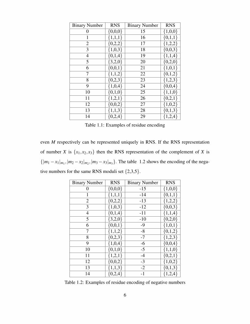
Binary Number RNS Binary Number RNS0 {0,0,0} 15 {1,0,0}1 {1,1,1} 16 {0,1,1}2 {0,2,2} 17 {1,2,2}3 {1,0,3} 18 {0,0,3}4 {0,1,4} 19 {1,1,4}5 {3,2,0} 20 {0,2,0}6 {0,0,1} 21 {1,0,1}7 {1,1,2} 22 {0,1,2}8 {0,2,3} 23 {1,2,3}9 {1,0,4} 24 {0,0,4}10 {0,1,0} 25 {1,1,0}11 {1,2,1} 26 {0,2,1}12 {0,0,2} 27 {1,0,2}13 {1,1,3} 28 {0,1,3}14 {0,2,4} 29 {1,2,4}
Table 1.1: Examples of residue encoding
even M respectively can be represented uniquely in RNS. If the RNS representation
of number X is {x1,x2,x3} then the RNS representation of the complement of X is
{|m1− x1|m1, |m2− x2|m2, |m3− x3|m3}. The table 1.2 shows the encoding of the nega-
tive numbers for the same RNS moduli set {2,3,5}.
Binary Number RNS Binary Number RNS0 {0,0,0} -15 {1,0,0}1 {1,1,1} -14 {0,1,1}2 {0,2,2} -13 {1,2,2}3 {1,0,3} -12 {0,0,3}4 {0,1,4} -11 {1,1,4}5 {3,2,0} -10 {0,2,0}6 {0,0,1} -9 {1,0,1}7 {1,1,2} -8 {0,1,2}8 {0,2,3} -7 {1,2,3}9 {1,0,4} -6 {0,0,4}10 {0,1,0} -5 {1,1,0}11 {1,2,1} -4 {0,2,1}12 {0,0,2} -3 {1,0,2}13 {1,1,3} -2 {0,1,3}14 {0,2,4} -1 {1,2,4}
Table 1.2: Examples of residue encoding of negative numbers
6

1.4 Arithmetic Operations
All the arithmetic operations performed on two integers in binary number system are
performed as modulo arithmetic operations on the residues in the residue number sys-
tem. Consider two binary numbers X , Y and the corresponding RNS representations
{x1,x2, · · · ,xn} and {y1,y2, · · · ,yn}. If Z =X opY , where op represents one of the arith-
metic operations of addition, subtraction, or multiplication, then Z = {z1,z2, · · · ,zn} in
RNS, where
zi = (xi op yi) mod mi,1≤ i≤ n
The calculation of zi depends only on xi and yi and does not interact with the
calculation of z j for j 6= i [18]. This property is termed as carry-free property of RNS.
The carry-free property holds only for addition, subtraction and multiplication opera-
tions while division and scaling operations result in complicated operations that involve
interactions between the residues. This is one of the main drawbacks of RNS. Hence
RNS is more advantageous for computation intensive applications involving simple
arithmetic operations like addition and multiplication. The application of RNS in gen-
eral purpose processors in limited as division and comparison are common operations
in general purpose processing.
The modulo operation is distributive over addition, subtraction and multiplica-
tion represented as,
|X op Y |m1 = ||X |m1 op |Y |m1|m1.
Since RNS arithmetic is modular arithmetic, the hardware of units are more complex
to build compared to conventional 2’s complement binary arithmetic units.
7

1.5 Conversion Algorithms
The overhead associated with the implementation of an RNS processor are the con-
version units that convert from a binary number system to RNS, and vice versa. This
conversion is unavoidable as the peripheral interfaces of most digital systems are based
on binary number system. A block diagram of a typical RNS processor is as shown
in 1.1. The input X to the RNS system is available as binary input. It is first converted
to residues. After processing the data, the result in the form of residues is converted
to the conventional binary representation. The process of converting binary number
to residues is called forward conversion and process of converting residues to binary
numbers is called reverse conversion.
Binary to Residue Converter
Residue to Binary Converter
X
. . .Mod m1Processor
Mod m2Processor
Mod mnProcessor
x1 x2 xn
y1 y2 yn
To Binary Systems
Figure 1.1: RNS Processor
8

Forward Conversion
Forward conversion involves the computation of remainders of input X with respect to
each modulus in the RNS moduli set. There are well known algorithms for forward con-
version [14, 17, 13, 11] in literature. The hardware complexity of the forward converter
depends on the type of moduli set selected. For arbitrary moduli sets like {2,5,7,11,19},
the forward conversion involves conventional way of calculating the remainders using
division algorithm. This is much complex to implement as combinational logic. Hence
look-up tables are used to implement forward converters for arbitrary moduli sets. For
special moduli sets like {2n,2n− 1,2n + 1} the architecture of forward converters is
simple and can be implemented in hardware using modulo adders and or carry save
adders due to the periodicity properties of the modulus of kind 2n,2n− 1 and 2n + 1.
The architecture of forward converter for special moduli is discussed in 3.
Numerical Example: Consider an RNS system with moduli set 4,3,5. The dy-
namic range of the system is 60 and numbers from -30 to 29 can be uniquely repre-
sented as residues. Some examples are listed in table1.3.
Binary Number x1 x2 x30 0 0 01 1 1 15 1 2 0
15 3 0 0-21 3 0 4-30 2 0 0
Table 1.3: Forward conversion examples
Reverse Conversion
Compared to forward conversion, reverse conversion is a much complex process and
its complexity is completely determined by the chosen moduli set. Reverse conver-
sion calculates the binary number X given the residues {x1,x2, ..,xn} and the moduli9

set {m1,m2, ..,mn}. Let M = ∏ni=1 mi be the dynamic range. There are two popular
algorithms in literature for reverse conversion.
• Reverse conversion (RC) based on the classical Chinese remainder theorem (CRT)
Given a set of relatively prime moduli {m1,m2, · · · ,mn}, the conventional repre-
sentation X of its residues {x1,x2, · · · ,xn} is calculated using the following math-
ematical model.
X = |n
∑i=1
xi|Mi|miMi|M, (1.4)
where, Mi = M/mi.
• RC based on New Chinese remainder theorem
Wang et.al [22] proposed a method for reverse conversion that is based on CRT
that is more efficient in terms of hardware implementation. It is mathematically
represented as,
X = |x1 +(x2− x1)k1m1 +(x3− x2)k2m1m2
+ · · ·+(xn− xn−1)kn−1m1 · · ·mn|M.
(1.5)
Notation |A|M indicates the remainder of A when divided with M. ki are the
multiplicative inverses such that,
k1m1 ∼= 1 (mod (m2 ∗m3 · · ·mn)),
k2m1m2 ∼= 1 (mod (m3 ∗m4 · · ·mn)),
...
kn−1m1m2 · · ·mn−1 ∼= 1(mod mn).
Example: Let the Binary representation of the residues {3,0,0} with respect to
the moduli set {4,3,5} be X . Here m1 = 4, m2 = 3, m3 = 5, and M = 60. The
multiplicative inverses of m1, m2 are k1 = 4, k2 = 3 respectively since k1m1 =
16 ∼= 1 mod m2m3, and k1m1m2 = 36 ∼= 1 mod m3. Substituting these values in
10
(1.5),
X = |3+(0−3)4∗4+(0−0)3∗4∗3|60,
X = |3−48|60 = |−45|60,
X = 60−45 = 15.
• Mixed radix conversion (MRC) algorithm
According to MRC [18], the mathematical model for the reconstruction of X is,
X = an
n
∏i=1
mi + · · ·+a3m2m1 +a2m1 +a1, (1.6)
where a1 = x1, a2 =∣∣∣(x2−a1)
∣∣m−11
∣∣m2
∣∣∣m2
and so on. |m−11 |m2 is the multiplica-
tive inverse of m1 modulo m2 such that |m−11 m1|m2 = 1.
Example: Considering the same example as above. In this case,
a1 = x1 = 3,
a2 = |4−1(0−3)|3
= |1(0−3)|3 = 0,
a3 = |3−1([4−1(0−3)]−0)|5
= |2([4(−3)]−0)|5 = 1.
Substituting a1, a2, and a3 in (1.6),
X = a1 +a2m1 +a3m1m2,
X = 3+0+1∗3∗4 = 15.
Mixed radix conversion is a sequential process and is generally slow to implement
reverse conversion compared to CRT based algorithms but it is simple to implement.
The application of MRC algorithm is generally limited to two or three-moduli sets.
The most popular algorithm used to implement reverse converter is Chinese remainder
theorem.
11

1.6 Applications
Due to the carry-free nature, residue number encoding has gained importance in high-
speed data processing applications where the critical path is associated with the prop-
agation of the carry. Using RNS encoding, the word-length of the data operands is
reduced and results in the minimization of critical path timing and in lower power
consumption. RNS is fault tolerant and error detection and correction is easy as it fa-
cilitates the isolation of faulty residues. Due to these attractive properties of RNS, it is
a promising alternative to conventional two’s complement number system. Although
RNS representation speeds up arithmetic operations like addition and multiplication, it
is much more complex to perform other operations like division, shifting, comparison
etc. This limits the application of RNS only to computationally intensive applications
that require mainly addition and multiplication operations. Hence RNS has gained
much popularity in the field of DSP and active research is going on in application of
RNS in the following fields: Digital filtering- FIR and IIR filters, Digital convolution,
Cryptography, Discrete Fourier, transform (DFT), Fast Fourier transform(FFT) proces-
sors, Digital image processing.
The use of RNS in general purpose processors where operations like division
and comparison are common, is limited as it is more efficient to implement those op-
erations in the conventional binary number system. As the RNS arithmetic operations
are performed on inputs of smaller input width, lower power and higher speed can be
expected.
12

Chapter 2
NEW RNS FOUR-MODULI SET FOR FIR FILTERS
2.1 Binary Vs RNS FIR Filter Architectures
The most popular use of RNS in the design of digital finite impulse response(FIR)
filters. FIR filters are highly stable architectures and are less sensitive to quantization
errors than filters of recursive architectures like Infinite impulse response (IIR) filters.
A digital FIR filter response of N-taps is mathematically represented as (2.1) where xn
is the the input data and a1,a2, · · · ,ak are the filter co-efficients.
yn =N
∑k=0
akxn−k (2.1)
Generally, two’s complement system (TCS) representation is widely chosen for the
binary representation of the input and co-efficients of a digital filter. FIR filters can
be implemented in hardware either in the Direct form, shown in the Fig 2.1 or in the
Transpose form shown in the Fig 2.2. Direct form results in larger critical path delay of
tD + tmul + tadder(N) compared to the critical path delay of the transposed form imple-
mentation which is tD + tmul + tadder. Here, tmul is the delay of the multiplier, tadder(N)
is the delay of the adder tree adding N inputs and tadder is a two-input adder delay and
tD is the delay of the register element. The Transpose form requires larger input buffers
for the input xn for it to be able to drive N multipliers. In general for ASIC implemen-
tations, the transpose form is preferred. For high speed implementations of transpose
form FIR filters, the result of the multiplier is represented in carry-save format and the
accumulator is implemented as carry save adder. The final stage of the such implemen-
tation of transpose form FIR filter is a conventional adder to add the carry save vectors
of the last stage.
The dynamic range of a N-tap FIR filter with input width of M bits and co-
efficient width of L bits is M + L+ log2N. As the number of taps increases, the dy-
namic range of the filter increases, and the delay of the output adder increases due to13

X X XX
Xn
Yn
ana1 a2a0
D D D
+
Figure 2.1: Direct form of FIR filters
MAC
X
+
X
+
X
+
X
Xn
Yn
an an-1 an-2 a0
DD D
Figure 2.2: Transposed form of FIR filters
longer carry-propagation [19]. Using RNS, the dynamic range can be decomposed into
smaller dynamic ranges and the MAC operations can be performed in parallel with-
out carry propagation among the channels. Consider an RNS system of p-moduli set
{m1,m2, · · · ,mp}. The mathematical representation of FIR filter using the p-moduli set
is,
y1,n =
∣∣∣∣∣ N
∑i=0|a1,k ∗ x1(n− k)|m1
∣∣∣∣∣m1
,
y2,n =
∣∣∣∣∣ N
∑i=0|a2,k ∗ x2(n− k)|m2
∣∣∣∣∣m2
,
...
yp,n =
∣∣∣∣∣ N
∑i=0|ap,k ∗ xp(n− k)|mp
∣∣∣∣∣mp
.
(2.2)
Here, a1,k,a2,k, · · · ,ap,k represent the residues of the filter co-efficients and x1,x2, · · · ,xp
represents the residues of the input. In RNS FIR filter using p-moduli set, there are p
filters operating in parallel without any inter-dependency. Due to parallelism and carry
free-property nature of RNS, high-speed FIR filters are realizable compared to conven-14

tional TCS representation. In addition to gain in performance, RNS filter architectures
result in low power in the following ways [5].
• Reduction in the peak current: Compared to conventional implementation of FIR
filters, RNS architectures uses smaller arithmetic units and less complex designs.
Hence, the peak current in each arithmetic unit decreases.
• Reduction in the switching activity: The reason mentioned above is applied for
smaller switching activities in RNS arithmetic units. As RNS systems operate
on smaller input widths, the switching activities are also relatively smaller. The
reduction in peak current as well as switching activity results in smaller dynamic
power.
• Several other circuit level power reduction techniques like voltage scaling in non-
critical paths using high threshold transistors can be applied very easily in RNS
circuits. The non-critical channel can be completely implemented using high
threshold transistors. In conventional binary systems, there are only specific
paths where high threshold transistors can be used.
The FIR filter architecture using RNS is as shown in Fig 2.3. The only overhead
in the implementation of RNS FIR filters is the conversion units from binary to RNS
and the reverse converter to convert the individual filter responses to binary response.
There are three basic steps in the implementation of RNS FIR filter using the moduli
set {m1,m2, · · · ,mp}.
1. Forward conversion: Let the input data sample at time n is X(n) and filter co-
efficients are ak. The data input and the filter co-efficients are converted to
15
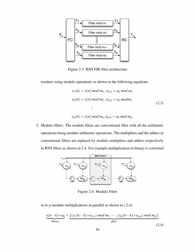
FC RC
Filter mod m1
Filter mod m2
Filter mod mp
Xn Yn
x2
xp-1
xp
x1 y1
y2
yp-1
yp
Filter mod mp-1
Figure 2.3: RNS FIR filter architecture
residues using modulo operations as shown in the following equations.
x1(n) = x(n) mod m1, a1,k = ak mod m1
x2(n) = x(n) mod m2, a2,k = ak modm2
...
xp(n) = x(n) mod mp,ap,k = ak mod mp
(2.3)
2. Modulo filters: The modulo filters are conventional filter with all the arithmetic
operations being modulo arithmetic operations. The multipliers and the adders in
conventional filters are replaced by modulo multipliers and adders respectively
in RNS filters as shown in 2.4. For example multiplication in binary is converted
MAC mod m
|+|m
x1,n
a1,n a1,n-1 a1,n-2 a1,0
D
|X|m |X|m |X|m |X|m
|+|mD |+|mD
Figure 2.4: Modulo Filter
in to p-modulo multiplications in parallel as shown in ( 2.4).
x(n− k)∗ak︸ ︷︷ ︸Binary
= {(x1(n− k)∗a1,k) mod m1, · · · ,(xp(n− k)∗ap,k) mod mp}︸ ︷︷ ︸RNS
(2.4)16

3. Reverse conversion: Individual filter responses y1,n,y2,n · · · ,yp,n to the final re-
sponse Yn = RC(y1,y2, · · · ,yp) using popular conversion algorithms discussed in
chapter 1.
2.2 A Study on Existing RNS Moduli Sets
Selection of moduli set is critical factor in determining the performance and power
of an RNS system. The moduli set selected to implement FIR filters should cover
the dynamic range of the filter. This in turn impacts the through put of the filter and
the hardware efficiency of the forward converter, reverse converter, and modulo MAC
units.
If n is the input width and assuming the filter coefficient width to be n, for an
Nth order FIR filter, the output width without scaling is 2n+ log2N. Hence the dynamic
range of the selected moduli set of the filter should be at least 2n+ log2N. For example,
for a 40 tap RNS FIR filter with 16 bit input width and 16 bit co-efficient width, the
dynamic range of the moduli set selected should be 32+ log240 = 36 bits. There are
two ways to achieve a higher dynamic range.
• Use a large number of moduli each with smaller magnitude: The moduli set con-
sists of large number of relatively prime numbers. An example for this type of
moduli set with dynamic range of 40 bits is {16,17,19,53,127,129,257}. Imple-
menting modulo arithmetic units using the moduli set is not simple. For this
reason, ROM table-lookup tables are used to implement modulo addition, sub-
traction and multiplications. Also increasing the number of moduli increases
the reverse converter complexity. Hence for large dynamic range applications,
moduli set of arbitrary prime moduli is not suitable for ASIC implementations.
• Use of small number of moduli with large magnitude: Examples for this type of
moduli set are {2n,2n−1,2n+1}, {2n,2n−1,2n+1,2n+1+1} etc. In these types
17

of moduli sets, the moduli are of the form 2n, 2n−1 and 2n +1 and the modulo
arithmetic blocks with respect to such moduli can be efficiently implemented as
digital VLSI circuits due to the special properties of the moduli.
To implement a RNS FIR filter of 40 bits dynamic range, some of the choices are
{214,214− 1,214 + 1}, {210,210− 1,210 + 1,211 + 1}. The popular moduli sets
of this form are the 3-moduli sets and the 4-moduli sets. There are few 5-moduli
sets proposed in literature but the design of the reverse converter is complex and
its overhead is substantially larger in terms of delay and power.
Three-moduli Sets
The most popular three-moduli set in the literature is {2n,2n− 1,2n + 1}. Its main
drawback is the larger difference in the critical path delays of the arithmetic channels.
The binary channel 2n is the fastest channel and the non-binary channel 2n + 1 is the
slowest channel owing to the architecture difference in the modular arithmetic units.
Any arithmetic operation modulo 2n is performed as conventional arithmetic operation
by discarding the higher order bits positioned after the bit position n. The arithmetic
operations modulo 2n + 1 are much more complex, and involve addition of correc-
tion factors and carry save addition involves end-around carries. This difference in the
speeds results in an inefficient distribution of computation load among different chan-
nels. To address this imbalance, [3, 4] proposed three -moduli set {2k,2n−1,2n +1},
k > n which has wider binary channel.
However, for smaller input widths and higher order filters, this moduli set does
not provide any performance improvement over conventional binary filter. For exam-
ple, consider a 8 bit wide filter with 64 taps. The dynamic range is 16+ log264 = 22.
The best suitable moduli set with dynamic range of 22 bits is {28,27−1,27+1} . In this
case, the modulo 2k filter operates on 8-bit inputs, as does conventional filter. In such
case we did not gain much advantage using RNS over conventional filter. For some
18

dynamic ranges, 3-moduli sets are advantageous. For example, if the input width is 16
and the filter taps are 8, the dynamic range is 35. The moduli set {213,211−1,211+1}
gives better speed compared to 2’s complement implementation as the number of bits
of MAC operation are reduced from 16 to 13. Hence for smaller input-widths, the
parallelism provided by 3-moduli set is insufficient.
An experimental study on RNS FIR filters implemented using the balanced 3-
moduli set {2k,2n− 1,2n + 1} was conducted to check the performance parameters.
Binary FIR filters and RNS FIR filter with the moduli set {2k,2n−1,2n+1} are imple-
mented in RTL and synthesized for minimum delay using commercial 65nm technology
library. Figure 2.5, and figure 2.6 show the area and delay comparison of Binary FIR
filters and RNS FIR filters with input and co-efficient widths of 24bits and figure 2.7,
and figure 2.8 are for input and co-efficient widths of 28 bits. From the delay plots, it is
observed that as the number of taps increases, the dynamic range increases and the ad-
vantage in speed by using RNS diminishes. It is also observed that the area advantage
in RNS filters is small, and is less than 9% in most of the designs.
0
0.2
0.4
0.6
0.8
1
0 10 20 30 40 50 60
Area
(mm
2)
Number of taps
Binary FilterRNS Filter
Figure 2.5: Comparison of area of Binary and RNS FIR filters with 24 bit input width
The experimental results show that the three-moduli set {2k,2n−1,2n +1} has19

2.6
2.8
3
3.2
3.4
3.6
3.8
4
0 20 40 60
Dela
y (n
s)
Number of taps
Binary FilterRNS Filter
Figure 2.6: Comparison of delay of Binary and RNS FIR filters with 24 bit input width
0
0.2
0.4
0.6
0.8
1
1.2
1.4
0 20 40 60
Area
(mm
2)
Number of taps
Binary FilterRNS Filter
Figure 2.7: Comparison of area of Binary and RNS FIR filters with 28 bit input width
smaller dynamic range and is not beneficial to implement higher order FIR filter archi-
tectures.
20
2.5
2.7
2.9
3.1
3.3
3.5
3.7
3.9
4.1
0 20 40 60
Dela
y (n
s)
Number of taps
Binary FilterRNS Filter
Figure 2.8: Comparison of delay of Binary and RNS FIR filters with 28 bit input width
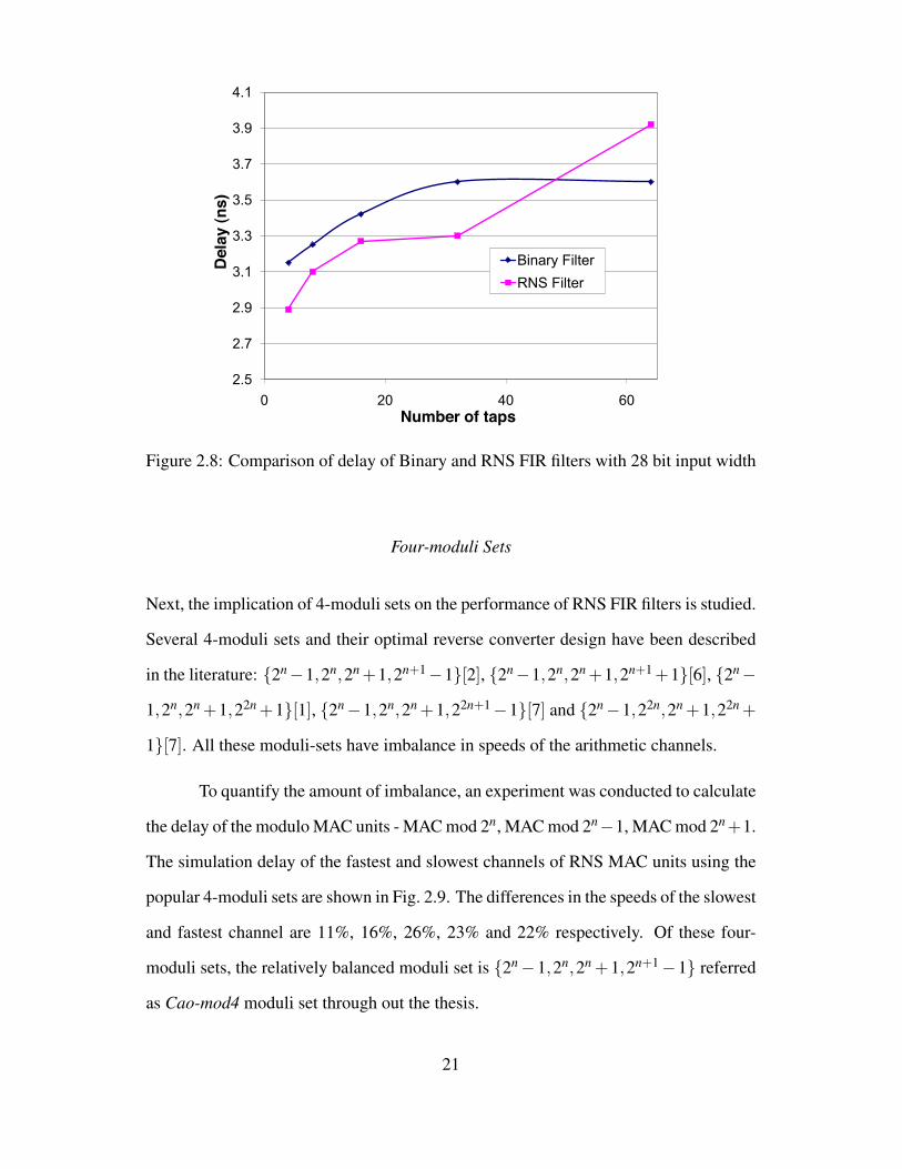
Four-moduli Sets
Next, the implication of 4-moduli sets on the performance of RNS FIR filters is studied.
Several 4-moduli sets and their optimal reverse converter design have been described
in the literature: {2n−1,2n,2n+1,2n+1−1}[2], {2n−1,2n,2n+1,2n+1+1}[6], {2n−
1,2n,2n+1,22n+1}[1], {2n−1,2n,2n+1,22n+1−1}[7] and {2n−1,22n,2n+1,22n+
1}[7]. All these moduli-sets have imbalance in speeds of the arithmetic channels.
To quantify the amount of imbalance, an experiment was conducted to calculate
the delay of the modulo MAC units - MAC mod 2n, MAC mod 2n−1, MAC mod 2n+1.
The simulation delay of the fastest and slowest channels of RNS MAC units using the
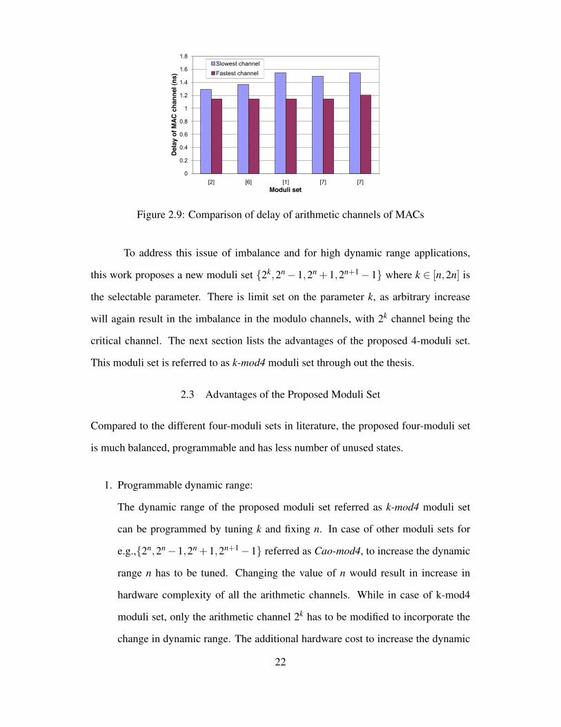
popular 4-moduli sets are shown in Fig. 2.9. The differences in the speeds of the slowest
and fastest channel are 11%, 16%, 26%, 23% and 22% respectively. Of these four-
moduli sets, the relatively balanced moduli set is {2n−1,2n,2n +1,2n+1−1} referred
as Cao-mod4 moduli set through out the thesis.
21
0
0.2
0.4
0.6
0.8
1
1.2
1.4
1.6
1.8
[2] [6] [1] [7] [7]De
lay
of M
AC c
hann
el (n
s)
Moduli set
Slowest channelFastest channel
Figure 2.9: Comparison of delay of arithmetic channels of MACs
To address this issue of imbalance and for high dynamic range applications,
this work proposes a new moduli set {2k,2n− 1,2n + 1,2n+1− 1} where k ∈ [n,2n] is
the selectable parameter. There is limit set on the parameter k, as arbitrary increase
will again result in the imbalance in the modulo channels, with 2k channel being the
critical channel. The next section lists the advantages of the proposed 4-moduli set.
This moduli set is referred to as k-mod4 moduli set through out the thesis.
2.3 Advantages of the Proposed Moduli Set
Compared to the different four-moduli sets in literature, the proposed four-moduli set
is much balanced, programmable and has less number of unused states.
1. Programmable dynamic range:
The dynamic range of the proposed moduli set referred as k-mod4 moduli set
can be programmed by tuning k and fixing n. In case of other moduli sets for
e.g.,{2n,2n−1,2n +1,2n+1−1} referred as Cao-mod4, to increase the dynamic
range n has to be tuned. Changing the value of n would result in increase in
hardware complexity of all the arithmetic channels. While in case of k-mod4
moduli set, only the arithmetic channel 2k has to be modified to incorporate the
change in dynamic range. The additional hardware cost to increase the dynamic
22

range in case of k-mod4 system is smaller to that Cao-mod4 RNS system.
Consider an example of n = 4, the moduli set {2n,2n−1,2n +1,2n+1−1} pro-
vides a dynamic range of 17 bits. To implement an application with 18 bits dy-
namic range in RNS using Cao-mod4 moduli set, n has to be chosen as 6 and the
moduli set is {26,26− 1,26 + 1,27− 1}. As n is even, the next available value
of n to tune for the higher dynamic range is 6. This will result in more hard-
ware associated with increased power consumption and delay of all the modulo
arithmetic channels. In case of k-mod4 moduli set k can be tuned to k = 5 and
with n = 4, we can achieve the dynamic range of 18 bits using the moduli set
{25,24−1,24 +1,25−1}.
2. Reduced number of unused states:
The number of unused states in a moduli set is calculated as the difference be-
tween the dynamic range required by an application and the dynamic range of-
fered by the moduli set. The fine programmability of dynamic range of the k-
mod4 moduli set by tuning k would also result in less number of unused states
for certain dynamic ranges compared to Cao-mod4 moduli set.
For example, a 16 order FIR filter with 16 bit wide input data and co-efficients
has a dynamic range of (2 ∗ 16+ log216) = 36 bits and the moduli set selected
to implement this filter should have a dynamic range of 36 bits or higher. To
implement this filter, n = 10 for Cao-Mod4 moduli set and n = 8, k = 12 for
k-mod4 moduli set. In this case,
the number of unused states for the Cao-mod4 moduli set
= (210(220−1)(211−1))−236 = 2129227940864 and
the number of unused states for the k-mod4 moduli set
= (211(216−1)(29−1))−236 = 68448948224.
3. Balanced moduli set:
23

The gap between the speed of the fastest binary channel and the slowest channel
is reduced by overloading the number of bits, the channel 2k operates on. But
arbitrary increase of k would again result in imbalance in the arithmetic channels,
hence the upper bound of k is limited to 2n.
2.4 Design of Reverse Converter
For the proposed moduli set {2k,2n−1,2n +1,2n+1−1}, a simple reverse conversion
model is derived based on the standard approach of design of 4-moduli set reverse
converters proposed in [2]. Let x1, x2, x3, and x4 represent the residues of a binary
number X with respect to the moduli 2k, 2n + 1, 2n− 1, and 2n+1− 1 respectively.
Given the residues and the moduli set, X can be reconstructed in two steps.
1. Partially reconstruct the binary number X1 of the original binary X from the
residues x1, x2, x3 with respect to the three-moduli set {2k,2n− 1,2n + 1}. X1
is obtained using the 3-moduli reverse converter proposed in [4]. X1 is repre-
sented as 22nY1 + x1 where Y1 is the intermediate result of 2n bits wide.
2. Create a single modulus from the three moduli set (2k,2n− 1,2n + 1) by multi-
plying the moduli i.e., modulus 2k(22n−1). Given X1, x4 and the two-moduli set
{2k(22n−1),2n+1−1}, X is reconstructed using MRC algorithm.
Reverse Converter Design for the Two-moduli Set {2k(22n−1),2n+1−1}
Reconstruction of the binary result from the residues X1 and x4 w.r.t the moduli set
{2k(22n−1),2n+1−1} is computed using MRC algorithm as follows,
X = a1 +a2P1, (2.5)
24

where
a1 = X1 = x1 +2kY1, (2.6)
a2 =∣∣∣(x4−X1)
(∣∣P−11
∣∣P2
)∣∣∣P2, (2.7)
P1 = 2k(22n−1), and (2.8)
P2 = 2n+1−1. (2.9)
∣∣P−11
∣∣P2
is the multiplicative inverse of P1 modulo P2 i.e,
|P−11 P1|P2 = 1. (2.10)
The multiplicative inverse of |P1|P2is given by the following lemma.
Lemma:
|P−11 |P2 =
∣∣(−1
3
)2n+3−k
∣∣2n+1−1 , k < n+3∣∣(−1
3
)22n+4−k
∣∣2n+1−1 , k ≥ n+3.
(2.11)
Proof: First |P1|P2 is simplified as follows,
|P1|P2 = |2k(22n−1)|2n+1−1
= |2k(2n−1(2n+1−1)+2n−1−1)|2n+1−1
= |2k(2n−1−1)|2n+1−1 = |2k−2(2n+1−4)|2n+1−1
= |2k−2(−3)|2n+1−1.
(2.12)
With this simplification, the lemma can be verified by substituting (2.11) and
(2.12) in (2.10).
Case 1: When k < n+3,
|P−11 P1|2n+1−1 =
∣∣∣∣(−13
)2n+3−k2k−2(−3)
∣∣∣∣2n+1−1
= |2n+1|2n+1−1 = 1.
(2.13)
25

Case 2: When k ≥ n+3,
|P−11 P1|2n+1−1 =
∣∣∣∣(−13
)22n+4−k2k−2(−3)
∣∣∣∣2n+1−1
= |22(n+1)|2n+1−1
=(|2n+1|2n+1−1
)(|2n+1|2n+1−1
)= 1.
(2.14)
In order to simplify the subsequent derivations,∣∣P−11
∣∣P2=∣∣∣(−1
3)2k′∣∣∣2n+1−1
, where
k′ =
n+3− k, k < n+3,
2n+4− k, k ≥ n+3.(2.15)
Knowing the multiplicative inverse, X is computed by substituting a1, a2 and
P1 from (2.6), (2.7) and (2.8) respectively in (2.5),
X = X1 +2k(22n−1)∣∣∣∣(x4−X1)
(−1
3
)2k′∣∣∣∣2n+1−1
= X1 +2k(22n−1)∣∣∣∣(1
3
)(X12k′− x42k′)
∣∣∣∣2n+1−1
= X1 +2k(22n−1)Z = x1 +Y12k +2k(22n−1)Z
= x1 +2k(Y1 +22nZ−Z).
(2.16)
In the above equations,
Z =∣∣∣(1
3
)(X12k′− x42k′)
∣∣∣2n+1−1
=C(A+B) (say), where
C =
∣∣∣∣(13
)∣∣∣∣2n+1−1
,
A =∣∣∣X12k′
∣∣∣2n+1−1
,
B =∣∣∣−x42k′
∣∣∣2n+1−1
.
The simplifications of A, B and C are given below.
A =∣∣∣X12k′
∣∣∣2n+1−1
=∣∣∣(x1 +2kY1
)2k′∣∣∣2n+1−1
= |A1 +A2|2n+1−1 ,
(2.17)
26

where A1 = | x1︸︷︷︸k
2k′|2n+1−1 and A2 = | Y1︸︷︷︸2n
2k+k′|2n+1−1.
Since x1 is a k bit vector and n≤ k≤ 2n, x1 is split into two vectors x11 and x12,
each of n+1 bits. This is done to remove the modular operation w.r.t 2n+1−1.
x11 = 0x1,k−1, · · · ,x1,k−n︸ ︷︷ ︸n+1
. (2.18)
x12 = 00 · · ·0︸ ︷︷ ︸2n−k+1
x1,k−n−1, · · · ,x1,0︸ ︷︷ ︸k−n
. (2.19)
With x = x11x12, A1 in (2.17) is computed as
A1 =∣∣∣(x112k−n + x12
)2k′∣∣∣2n+1−1
=∣∣∣x112k−n+k′+ x122k′
∣∣∣2n+1−1
= |A11 +A12|2n+1−1 .
(2.20)
where
A11 = x11,n−k′11, · · · ,x11,0︸ ︷︷ ︸
n+1−k′11
x11,n, · · · ,x11,n−k′11+1︸ ︷︷ ︸k′11
, (2.21)
A12 = x12,n−k′, · · · ,x0︸ ︷︷ ︸n+1−k′
x12,n, · · · ,x12,n−k′+1︸ ︷︷ ︸k′
, and (2.22)
k′11 = |k−n+ k′|n+1. (2.23)
In a similar fashion to splitting of x1, Y1 is also split into two vectors of n+ 1
bits.
Y11 = 00Y1,2n−1, · · · ,Y1,n+1︸ ︷︷ ︸n−1
. (2.24)
Y12 = Y1,n, · · · ,Y1,0︸ ︷︷ ︸n+1
. (2.25)
27

A2 is computed with Y11 and Y12 as follows,
A2 =∣∣∣(Y112n+1 +Y12)2k+k′
∣∣∣2n+1−1
=∣∣∣Y112n+1+k+k′+Y122k+k′
∣∣∣2n+1−1
= |A21 +A22|2n+1−1 ,
(2.26)
where
A21 = Y11,n−k′21, · · · ,Y11,0︸ ︷︷ ︸
n+1−k′21
Y11,n, · · · ,Y11,n−k′21+1︸ ︷︷ ︸k′21
, (2.27)
A22 = Y12,n−k′22, · · · ,Y11,0︸ ︷︷ ︸
n+1−k′22
Y12,n, · · · ,Y12,n−k′22+1︸ ︷︷ ︸k′22
, (2.28)
k′21 = |n+1+ k+ k′|n+1, k′22 = |k+ k′|n+1. (2.29)
Simplifying B and C,
B =∣∣∣−x42k′
∣∣∣2n+1−1
= x̄4,n−k′, · · · , x̄0︸ ︷︷ ︸n+1−k′
x̄4,n, · · · , x̄4,n−k′+1︸ ︷︷ ︸k′
. (2.30)
C =
∣∣∣∣(13
)∣∣∣∣2n+1−1
=n/2
∑i=0
22i [2]. (2.31)
28

Chapter 3
RNS FIR Filter Implementation
RNS implementation of FIR filter using the proposed moduli set comprise of the fol-
lowing components forward converters, modulo MAC blocks and a reverse converter
as shown in Figure 3.1. This chapter details the implementation of each component in
building the complete RNS FIR filter.
FC RC
Filter mod 2k
Filter mod 2n-1
Filter mod 2n+1
Filter mod 2n+1-1
Xn Yn
x2
x3
x4
x1 y1
y2
y3
y4
Figure 3.1: RNS implementation of a FIR filter
Forward Converter
The forward converter for this moduli set has 4 units that calculate the residue of the
input with respect to moduli 2k, 2n−1, 2n +1, and 2n+1−1.
• Modulo 2k: If X is the input of p bits wide, then X mod 2k is simply calculated
by discarding the most significant bits to the kth bit position. This does not
require additional hardware except routing. For example if X is represented as
Xp−1Xp−2 · · ·X0, then X mod 2k = Xk−1 · · ·X0.
• Modulo 2n − 1(Modulo 2n+1 − 1): There are popular algorithms to calculate
residues of the modulo of kind 2n−1. For the present implementation of modulo
29

2n− 1 and modulo 2n+1− 1 operations, architecture proposed in [11] is used.
First step in the process of modulo calculation is to represent input X in slices
of n (n + 1) bits. These operands generated are added using a multi-operand
modulo adder (MOMA). A MOMA comprises of carry save adders (CSA) with
end-around-carry to reduce multiple operands to two vectors (carry vector and
save vector) of n bits wide. These two vectors are added using a modulo 2n− 1
adder. An example of a carry save addition of three inputs with EAC is shown in
Figure 3.2. An example of CSA tree that reduces 5 input operands of n bits wide
to two carry and save vectors is as shown in Figure 3.3. If S, C are the output
x1x2x3 x0Y1 Y0Y3 Y2
S1 S0S3 S2C1 C0C3 C2 C3
Z1 Z0Z3 Z2
101111010101--------00111011
EAC
Figure 3.2: Example of a CSA with end-around-carry
vectors of CSA tree then,
(S+C) mod (2n−1) =
S+C, S+C < (2n−1),
S+C− (2n−1), S+C ≥ (2n−1).(3.1)
The modulo 2n−1 adder can be implemented using a ripple carry adder with its
carry out bit being fed back as its carry in (cin) bit. The critical path of such
adder of n bits wide will be 2n full adder delays. Instead, it can be implemented
as two ripple carry adders operating in parallel with cin=0 and cin=1 as carry in
bits and a mux as shown in Figure 3.4. The critical path delay in this case is n full30

CSA
CSA
CSA
Figure 3.3: Example of 5 input CSA
adder delay and a 2:1 mux delay. This high speed implementation of the modulo
adder is used in the current design.
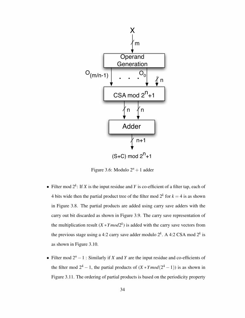
• Modulo 2n +1 : The architecture of modulo 2n +1 residue generator is same as
that of modulo 2n−1 residue generator. The general architecture of it has three
units - operand generation unit, CSA tree with EAC and a modulo 2n +1 adder.
The input bits are arranged using the periodicity property of the moduli 2n+1 as
operands of n bits. The operands generated and the correction factor are added
using carry save adders modulo 2n + 1. The modulo 2n + 1 carry save addition
is as explained in Figure 3.5. The final result is calculated using modulo 2n + 1
adder. If S, C are the output vectors of CSA tree, then the result of the modulo
adder is as follows:
(S+C) mod (2n +1) =
S+C, S+C ≤ (2n +1),
S+C− (2n +1), S+C > (2n +1).(3.2)
31

Mux0 1
S C
Cin=0 Cin=1Adder Adder
Sel
Cout
n n
(S+C) mod 2n-1
n
Figure 3.4: Modulo 2n−1 adder
x1x2x3 x0Y1 Y0Y3 Y2
S1 S0S3 S2
C1 C0C3 C2 ~C3
Z1 Z0Z3 Z2
001101011000--------11100011
EAC Cor = -1
Figure 3.5: Example of a CSA mod 2n +1 addition
A modulo 2n + 1 adder again requires two adders operating in parallel and a
2:1 mux to select the correct output. But the hardware requirements of modulo
2n +1 adder in the implementation of FIR filters can be reduced by representing32
output as intermediate sum. Instead of representing the output as the final modulo
result, an intermediate result is generated by adding the sum and carry vectors
from the CSA tree using conventional addition. As there are n+1 bits available
to represent the result and S,C are of only n bits wide, S+C mod (2n + 1) can
always be represented as S+C. For example, consider n = 4. The outputs of
the CSA tree are of 4 bits wide and the final modulo is of 5 bits wide. Let
S = 9, C = 12. Then according to 3.2,
S+C mod (2n +1) = S+C− (2n +1),
9+12 mod (24 +1) = 9+12−17 = 4.
By using conventional addition, the result is S +C = 21 which can be safely
represented in 5 bits. This intermediate result still carry information about the
final modulo result as 21mod(24+1) = 4. As there are further modulo operations
in the modulo filters, this intermediate representation would not impact the filter
output. The hardware architecture of the residue generator of modulo 2n+1 is as
shown in Figure 3.6
Modulo FIR Filters
Modulo FIR filters are realized in transpose form to reduce the critical path delay of
the RNS filter. The output of each tap is represented in carry save (CS) form. CS rep-
resentation avoid the computation of modular addition in each tap and computation of
final moduli in each channel is carried out in the last stage. The only drawback in the
CS representation of the accumulated result of each tap is increase in the number of
registers required in each stage. Compared to conventional representation of accumu-
lated result as final sum, CS representation requires double the number of registers to
propagate both carry and save vectors to the next stage. The general architecture of a
modulo filter is as shown in Figure 3.7.
The three different kinds of modulo filters are explained below:33
.. .
Operand Generation
CSA mod 2n+1
Adder
Xm
nO0O(m/n-1)
nn
n+1
(S+C) mod 2n+1
Figure 3.6: Modulo 2n +1 adder
• Filter mod 2k: If X is the input residue and Y is co-efficient of a filter tap, each of
4 bits wide then the partial product tree of the filter mod 2k for k = 4 is as shown
in Figure 3.8. The partial products are added using carry save adders with the
carry out bit discarded as shown in Figure 3.9. The carry save representation of
the multiplication result (X ∗Y mod2k) is added with the carry save vectors from
the previous stage using a 4:2 carry save adder modulo 2k. A 4:2 CSA mod 2k is
as shown in Figure 3.10.
• Filter mod 2n−1 : Similarly if X and Y are the input residue and co-efficients of
the filter mod 24− 1, the partial products of (X ∗Y mod(24− 1)) is as shown in
Figure 3.11. The ordering of partial products is based on the periodicity property
34

.. .Mod PPG
Mod CSA
4:2 Mod CSA
Xi
P0Pn
Yi
S C
Si Ci
Si-1
Ci-1
Figure 3.7: RNS modulo filter components
x0x0x0 x0Y1 Y0Y3 Y2
x1x1x1 0Y0Y2 Y1
x2x2 0Y1 Y0 0
x3 0Y0 00Figure 3.8: Partial product generation mod 24
of the moduli 2n−1 as explained in the equation 3.3.
|2i|2n−1 = 2|i|n (3.3)
35

x1x2x3 x0Y1 Y0Y3 Y2
S1 S0S3 S2C1 C0C2
Z1 Z0Z3 Z2
101111010101--------00111010
0
Figure 3.9: Carry save addition mod 24
CSA mod m
CSA mod m
Si-1 Ci-1Sm Cm
Si Ci
Figure 3.10: 4:2 Carry save accumulator
x0x0x0 x0Y1 Y0Y3 Y2
x1x1x1 Y0Y2 Y1
x2x2Y1 Y0
x3Y0
x1Y3x2Y3 x2Y2
x3Y3 x3Y2 x3Y1Figure 3.11: Partial product generation mod 24−1
The partial products generated are added using carry save adders modulo 2n−1.
The carry save adder with end around carry is as shown in 3.2. The final carry and
36

sum vector result of the multiplication is added with the carry and save vectors
from the previous stage using a 4:2 carry save adder modulo 2n−1.
• Filter mod 2n+1: The architecture of multiplication modulo 2n+1 is as followed
in [23]. The partial products if the input residues of n+1 bits wide are arranged
as vectors of n bits wide. The partial product generation for inputs of 5 bits
wide is as shown in Figure 3.12. The carry save adder with end around carry
for modulo 24 + 1 is as shown in Figure 3.5. The arrangements of the partial
x0x0x0 x0Y1 Y0Y3 Y2
x1x1x1 Y0Y2 Y1
x2x2Y1 Y0
x3Y0
x1Y3
x2Y3 x2Y2
x3Y3 x3Y2 x3Y1 Cor = -7
x1Y3
x2x2Y3 Y2
x3Y1x3x3Y3 Y2
x0Y4
x1Y4
x2Y4
x3Y4
x4Y3 x4Y2 x4Y1 x4Y0x4Y0x4x4Y2 Y1x4Y3x4Y4
x1Y4x2Y4x3Y4
x4Y4
x0Y4
Cor = -3
Cor = -1
Cor = -15
Cor = -15
Figure 3.12: Partial product generation mod 24 +1
products is based on the periodicity property of moduli 2n+1 as explained in the
equation 3.4.
|2i|2n+1 = 2|i|2n ,2 j ≤ i < (2 j+1)
|2i|2n+1 =−2|i|n,(2 j−1)< i≤ 2 j
j > 1
(3.4)
The partial product vectors are added using carry save adders modulo 2n+1. The
carry save results of the multiplication are added to the carry save vectors of n+1
bits wide from the previous stage using a 4:2 CSA mod 2n +1.
37
Reverse Converter Design for the Two Moduli Set {2k(22n−1),2n+1−1}
In this section the details of the Step 2 of the reverse converter design mentioned in
chapter 2 is presented. The details of the derivation of this reverse converter can be
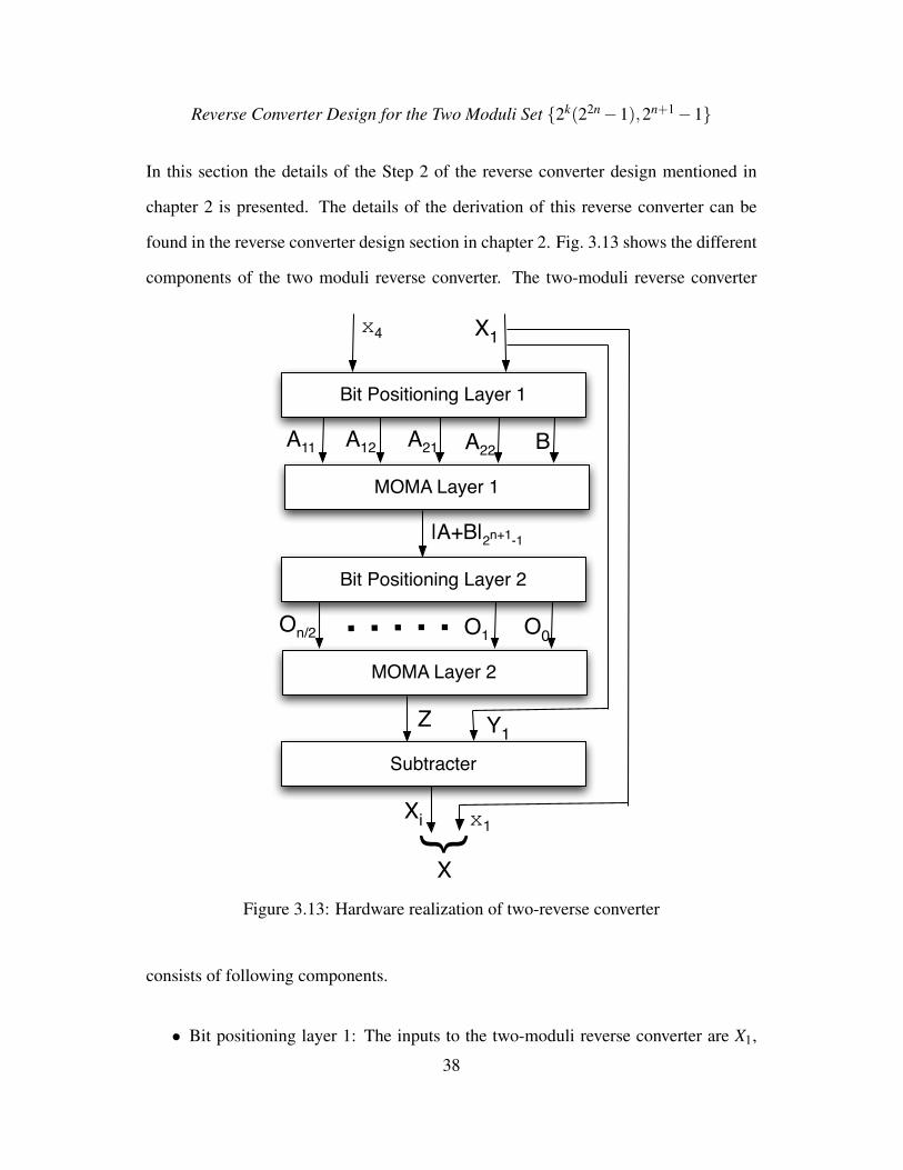
found in the reverse converter design section in chapter 2. Fig. 3.13 shows the different
components of the two moduli reverse converter. The two-moduli reverse converter
Bit Positioning Layer 1
MOMA Layer 1
Bit Positioning Layer 2
MOMA Layer 2
Subtracter
A11 A12 A21 A22 B
Z
|A+B|2n+1-1
On/2 O1 O0
{
X1x4
x1Xi
X
Y1
Figure 3.13: Hardware realization of two-reverse converter
consists of following components.
• Bit positioning layer 1: The inputs to the two-moduli reverse converter are X1,
38
the partial reconstructed binary number from the three-moduli reverse converter
of the moduli set {2k,2n−1,2n +1} and x4, the residue of X with respect to the
modulus (2n+1−1). X1 is computed as [3]
X = 22nY1 + x1, (3.5)
where Y1 is 2n bit wide intermediate result of the three-moduli reverse converter.
The output of the bit positioning layer 1 are A11, A12, A21, A22 and B, each is
n+1 bits wide. The bit ordering of these outputs defined in derivation of reverse
converter model are as follows.
A11 = x11,n−k′11, · · · ,x11,0︸ ︷︷ ︸
n+1−k′11
x11,n, · · · ,x11,n−k′11+1︸ ︷︷ ︸k′11
, (3.6)
A12 = x12,n−k′, · · · ,x0︸ ︷︷ ︸n+1−k′
x12,n, · · · ,x12,n−k′+1︸ ︷︷ ︸k′
, and (3.7)
k′11 = |k−n+ k′|n+1, (3.8)
A21 = Y11,n−k′21, · · · ,Y11,0︸ ︷︷ ︸
n+1−k′21
Y11,n, · · · ,Y11,n−k′21+1︸ ︷︷ ︸k′21
, (3.9)
A22 = Y12,n−k′22, · · · ,Y11,0︸ ︷︷ ︸
n+1−k′22
Y12,n, · · · ,Y12,n−k′22+1︸ ︷︷ ︸k′22
, (3.10)
k′21 = |n+1+ k+ k′|n+1, (3.11)
k′22 = |k+ k′|n+1,and (3.12)
B =∣∣∣−x42k′
∣∣∣2n+1−1
= x̄4,n−k′, · · · , x̄0︸ ︷︷ ︸n+1−k′
x̄4,n, · · · , x̄4,n−k′+1︸ ︷︷ ︸k′
. (3.13)
Computation of B requires n+1 inverters and no additional hardware is required
for the ordering of the bits.
• Multi-operand modulo addition (MOMA) layer 1: A MOMA [11] is basically a
modulo adder, but can be doubled as a compressor as the output bit width is fixed
by the modulo operation irrespective of the number of operands. The MOMA
39

used here takes five input vectors A11, A12, A21, A22 and B of n + 1 bits and
added using carry save adders (CSA) with end-around carry (EAC). The carry
and save bits of the output of the adder are added with a modulo (2n+1 − 1)
adder to produce the output denoted by |A+B|2n+1−1, which is n+ 1 bit wide.
This MOMA layer requires 4(n+1) full adders (FA), including the (n+ 1) FAs
required by the 2n+1−1 modulo adder.
• Bit positioning layer 2: This layer is same as the bit positioning layer 1, except
that this layer generates (n/2+ 1) operands, O0, O1, . . . , On/2, each of n+ 1
bits obtained from ordering of the bits of |A+B|2n+1−1, from the output of the
MOMA layer 1. The details of the ordering the bits can be found in the derivation
of reverse converter model in chapter 2. Unlike the bit positioning layer 1, this
layer does not require any gates.
• MOMA layer 2: This layer is similar to MOMA layer 1, except that the number
of inputs are (n/2+1), viz. O0, O1, . . . , On/2. The total number of FAs required
to implement this MOMA is (n/2)(n+ 1), including (n+ 1) FAs of the modulo
(2n+1−1) adder. The output of this layer is n+1 bit and is denoted by Z.
• Subtracter: Here the output Z of MOMA layer 2 is left shifted by 2n bits and
added to Y1. The resultant 3n+1 bit vector is as shown below
Zn, · · · ,Z1,Z0︸ ︷︷ ︸n+1
,
2n︷ ︸︸ ︷Y1,2n−1, · · · ,Y1,1,Y1,0
Z is subtracted from this result to generate the intermediate result Xi, which is
left shifted by k bits and added to the residue x1 (k bit wide) to get the final result
X .
X = x1 +Y12k +2k(22n−1)Z
The 3n+1 bit subtracter is implemented as a 2’s complement adder and requires
(3n+1) FAs.
40

Chapter 4
Experimental Results
4.1 Performance of MAC units
In this section, the advantages of the proposed 4-moduli set k-mod4 moduli set over
the Cao-mod4 moduli set is illustrated by implementing modulo MAC units. Area, de-
lay and power consumption of an RNS filter is usually dominated by the MACs as the
conversion overhead of the forward and the reverse converter remains constant, while
the number of MACs increases linearly with the order of the filter. Hence the measure-
ments of the area and the power of the MAC units alone is considered to compare the
advantages of the k-mod4 moduli set with the Cao-mod4 moduli set.
An RNS MAC unit consists of modulo MACs for each moduli in the moduli
set. Of all the modulo MACs, the modulo MAC for the modulus 2n +1 has the longest
delay [3]. There have been several implementations to minimize the delay of the MAC
associated with the 2n + 1 channel. Of these [23] was found to be efficient and it is
used in the RNS filter implementations. MACs for moduli 2n and 2k are implemented
as conventional binary MACs with the MSB bits greater than 2n and 2k discarded re-
spectively. MACs for moduli (2n−1) and (2n+1−1) are implemented as conventional
binary MACs with end around carry added to the LSB.
In the experiments, the area and the power of the modulo MACs for the dynamic
ranges 9–105 are compared. Selection of n and k for the moduli sets {2n1,2n1−1,2n1+
1,2n1+1− 1} (Cao-mod4) and {2k,2n2− 1,2n2 + 1,2n2+1− 1} (k-mod4) are shown in
Table ??. Due to the absence of the programmable k, Cao-mod4 uses higher n, while
the k-mod4 moduli set can be programmed to cover the intermediate dynamic range
with smaller n as can be seen from the table. However, k cannot be increased arbitrarily
as it is upper bounded by the critical path of the 2n+1 channel (critical path condition),
which cannot exceed the delay of the binary channel 2k.
41

Dynamic Range n1 n2 k Dynamic range n1 n2 k9 2 2 2 55 14 12 18
10 4 2 3 56 14 12 1911 4 2 4 57 14 14 1412 4 4 4 58 16 14 1413 4 4 4 59 16 14 1514 4 4 4 60 16 14 1615 4 4 4 61 16 14 1716 4 4 4 62 16 14 1817 4 4 4 63 16 14 1918 6 4 5 64 16 14 2019 6 4 6 65 16 16 1620 6 4 7 66 18 16 1721 6 4 8 67 18 16 1822 6 6 6 68 18 16 1923 6 6 6 69 18 16 2024 6 6 6 70 18 16 2125 6 6 6 71 18 16 2226 8 6 7 72 18 16 2327 8 6 8 73 18 18 1828 8 6 9 74 20 18 1829 8 6 10 75 20 18 1930 8 6 11 76 20 18 2031 8 6 12 77 20 18 2132 8 8 8 78 20 18 22
Table 4.1: Dynamic ranges used in the experiments
42
Dynamic Range n1 n2 k Dynamic range n1 n2 k33 8 8 8 79 20 18 2334 10 8 9 80 20 18 2435 10 8 10 81 20 20 2036 10 8 11 82 22 20 2137 10 8 12 83 22 20 2238 10 8 13 84 22 20 2339 10 8 14 85 22 20 2440 10 8 15 86 22 20 2541 10 10 10 87 22 20 2642 12 10 11 88 22 20 2743 12 10 12 89 22 22 2244 12 10 13 90 24 22 2345 12 10 14 91 24 22 2446 12 10 15 92 24 22 2547 12 10 16 93 24 22 2648 12 10 17 94 24 22 2749 12 12 12 95 24 22 2850 14 12 13 96 24 22 2951 14 12 14 97 24 24 2452 14 12 15 98 26 24 2553 14 12 16 99 26 24 2654 14 12 17 100 26 24 27
Table 4.2: Dynamic ranges used in the experiments
43
For the experiments, the modulo MACs are implemented in RTL and synthe-
sized using a 65nm standard cell library. The area and the power comparisons of the
MAC units using the k-mod4 and the Cao-mod4 moduli sets synthesized at the maxi-
mum frequency of 200 MHz and 500 MHz are presented in Figs. 4.1 and 4.2, and in
Figs. 4.3 and 4.4 respectively. Improvement in area and power reduction is observed
for all dynamic ranges. From the plots, area reduction as much as 46% and power
reduction as much as 43% are observed.
0.000
0.010
0.020
0.030
0.040
0.050
0.060
0.070
0 20 40 60 80 100
Are
a (
mm
2)
Dynamic range (bits)
k-mod4
cao-mod4
A
B
46%
Figure 4.1: Comparisons of area of modular MACs for k-mod4 and Cao-mod4 synthe-sized at 200MHz
It can be seen that the synthesized area of MACs using Cao-mod4 moduli set for
the dynamic range spanned between two consecutive ns i.e, n and n+ 2 remains con-
stant (Annotated portion A in Fig. 4.1). This is due to the absence of a programmable
moduli set, which can customize the hardware corresponding to the required dynamic
range. For example the dynamic range of the Cao-mod4 moduli set, when n = 4 is
4n+ 1 = 17bits. But for the next immediate dynamic range of 18 bits, n = 4 is not
sufficient and the next available value is n = 6. However in case of k-mod4 moduli set,
to achieve dynamic range of 18 bits, k can be programmed to k = 5, with n = 4.
Another observation from the area and the power plots for the k-mod4 moduli44

0.000
0.005
0.010
0.015
0.020
0.025
0.030
0 20 40 60 80 100
Pow
er (W
)
Dynamic range (bits)
k-mod4cao-mod4
43%
14%
Figure 4.2: Comparisons of power of modular MACs for k-mod4 and Cao-mod4 syn-thesized at 200MHz
0.000
0.010
0.020
0.030
0.040
0.050
0.060
0.070
0.080
0.090
0.100
0 20 40 60 80 100
Are
a (
mm
2)
Dynamic range (bits)
k-mod4
cao-mod4
45%
20%
Figure 4.3: Comparisons of area of modular MACs for k-mod4 and Cao-mod4 synthe-sized at 500MHz
set is that there are sudden jumps in the area and the power at certain dynamic ranges
(Annotated portion B in Fig. 4.1). This is due to the critical path condition , that
disallows k from increasing beyond a certain value, and forces to choose the next higher
n.
45
0
0.01
0.02
0.03
0.04
0.05
0.06
0.07
0.08
0 20 40 60 80 100
Pow
er (
W)
Dynamic range (bits)
k-mod4cao-mod4
42% Same power when n=k
18%
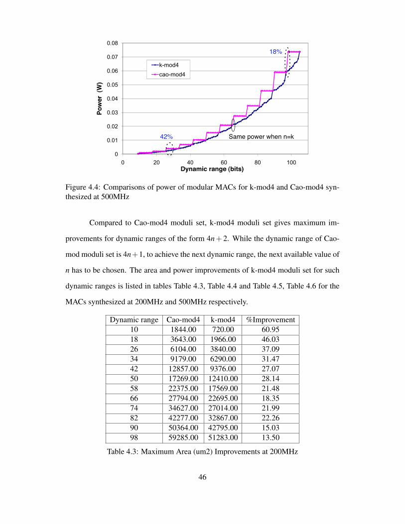
Figure 4.4: Comparisons of power of modular MACs for k-mod4 and Cao-mod4 syn-thesized at 500MHz
Compared to Cao-mod4 moduli set, k-mod4 moduli set gives maximum im-
provements for dynamic ranges of the form 4n+2. While the dynamic range of Cao-
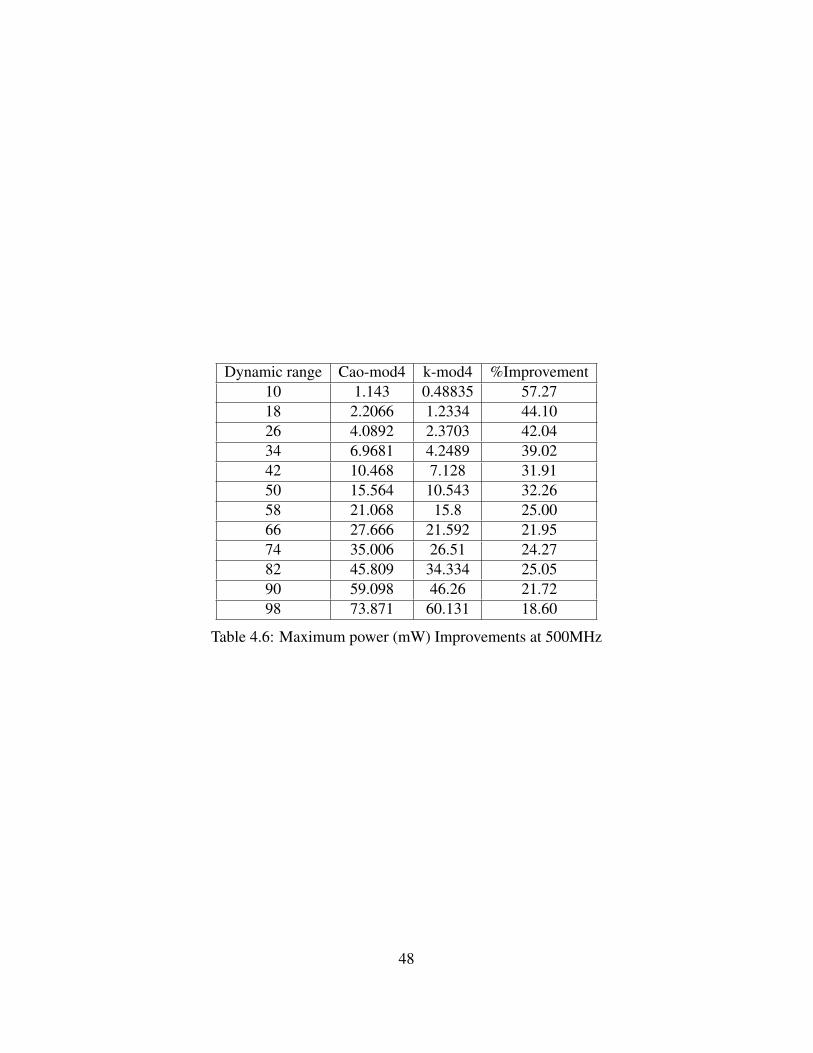
mod moduli set is 4n+1, to achieve the next dynamic range, the next available value of
n has to be chosen. The area and power improvements of k-mod4 moduli set for such
dynamic ranges is listed in tables Table 4.3, Table 4.4 and Table 4.5, Table 4.6 for the
MACs synthesized at 200MHz and 500MHz respectively.
Dynamic range Cao-mod4 k-mod4 %Improvement10 1844.00 720.00 60.9518 3643.00 1966.00 46.0326 6104.00 3840.00 37.0934 9179.00 6290.00 31.4742 12857.00 9376.00 27.0750 17269.00 12410.00 28.1458 22375.00 17569.00 21.4866 27794.00 22695.00 18.3574 34627.00 27014.00 21.9982 42277.00 32867.00 22.2690 50364.00 42795.00 15.0398 59285.00 51283.00 13.50
Table 4.3: Maximum Area (um2) Improvements at 200MHz
46

Dynamic range Cao-mod4 k-mod4 %Improvement10 0.871 0.397 54.4218 1.656 0.943 43.0826 2.775 1.772 36.1634 4.128 2.840 31.2142 5.716 4.217 26.2350 7.606 5.892 22.5358 9.834 7.702 21.6866 12.147 9.973 17.9074 15.340 11.957 22.0582 18.960 14.443 23.8290 22.859 19.154 16.2198 27.325 23.347 14.56
Table 4.4: Maximum Area (um2) Improvements at 500MHz
Dynamic range Cao-mod4 k-mod4 %Improvement10 1793.000 721.000 59.7918 3526.000 1917.000 45.6326 6354.000 3742.000 41.1134 10241.000 6590.000 35.6542 14448.000 10485.000 27.4350 20212.000 14552.000 28.0058 26714.000 20544.000 23.1066 34077.000 27207.000 20.1674 42659.000 33201.000 22.1782 55011.000 41832.000 23.9690 68419.000 55652.000 18.6698 87410.000 69753.000 20.20
Table 4.5: Maximum power (mW) Improvements at 200MHz
47
Dynamic range Cao-mod4 k-mod4 %Improvement10 1.143 0.48835 57.2718 2.2066 1.2334 44.1026 4.0892 2.3703 42.0434 6.9681 4.2489 39.0242 10.468 7.128 31.9150 15.564 10.543 32.2658 21.068 15.8 25.0066 27.666 21.592 21.9574 35.006 26.51 24.2782 45.809 34.334 25.0590 59.098 46.26 21.7298 73.871 60.131 18.60
Table 4.6: Maximum power (mW) Improvements at 500MHz
48

4.2 Performance of Reverse Converter
In this section, the hardware complexity and the delay of the proposed k-mod4 reverse
converter is compared with the existing 4-moduli reverse converters. Cao-mod4 moduli
set {2n,2n−1,2n +1,2n+1−1} [2] has been chosen for comparison with the proposed
reverse converter as it is the most balanced among the existing 4-moduli sets.
In the proposed k-mod4 moduli set {2k,2n−1,2n +1}, if k = n, then the hard-
ware complexity and the delay of k-mod4 reverse converter is identical to the Cao-mod4
reverse converter. Hence it is assumed that k > n for comparison in this section.
Recall that reverse converter design of a 4-moduli set consists of two stages as
mentioned in design of reverse converter section. In the first stage, the residues are
processed through a 3-moduli set. For k > n, k-mod4 reverse converter will contain an
additional CSA layer of 2n FAs over Cao-mod4 in the first stage. Also, k-mod4 incurs
an additional FA delay over Cao-mod4 in stage 1. Similarly, in the second stage, the
reverse converter for the two-moduli set {2k(22n−1),2n+1−1} requires an additional
CSA layer of n+ 1 FAs and incurs extra FA delay over the reverse converter of the
two-moduli set {2n(22n−1),2n+1−1}.
Table 4.7 shows the detailed comparison of area, delay of the reverse converters
for the proposed k-mod4 and the Cao-mod4 reverse converters. Note that tINV , tMUX
and tFA denote the gate delays of inverter, MUX and full adder respectively. l is the
number of stages in the n/2+1 CSA tree.
The proposed reverse converter and the four-stage reverse converter for the Cao-
mod4 moduli set [2] are synthesized using a 65nm standard cell library. The designs
are optimized for minimum delay. The minimum delay of the reverse converters for
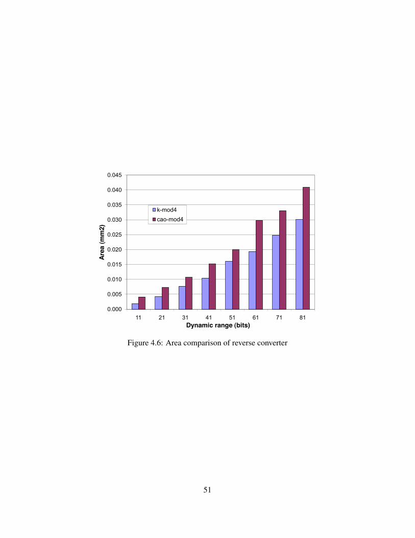
different dynamic ranges are compared in Fig. 4.5 and their corresponding areas are
compared in Fig. 4.6. The synthesis results show that for a given dynamic range, our
49

Gates k-mod4 RC Cao-mod4 RCINV 2n+ k+2 3n+2HA 0 1FA n2/2+27n/2+2 n2/2+21n/2+4
MUX 0 2
DelaytINV+ tINV + tMUX
(11n+10+ l)tFA +(11n+8+ l)tFADyn. range 3n+ k+1 4n+1
Table 4.7: Area and delay comparison of 4-moduli sets
k-mod4 reverse converter has 23% less delay and 54% less area. Note that the reverse
converter implementations of both the moduli sets are same when k = n.
0.00
0.50
1.00
1.50
2.00
2.50
3.00
3.50
4.00
11 21 31 41 51 61 71 81
Dela
y (n
s)
Dynamic range
k-4modcao-4mod
Figure 4.5: Delay comparison of reverse converter
50
0.000
0.005
0.010
0.015
0.020
0.025
0.030
0.035
0.040
0.045
11 21 31 41 51 61 71 81
Area
(mm
2)
Dynamic range (bits)
k-mod4cao-mod4
Figure 4.6: Area comparison of reverse converter
51
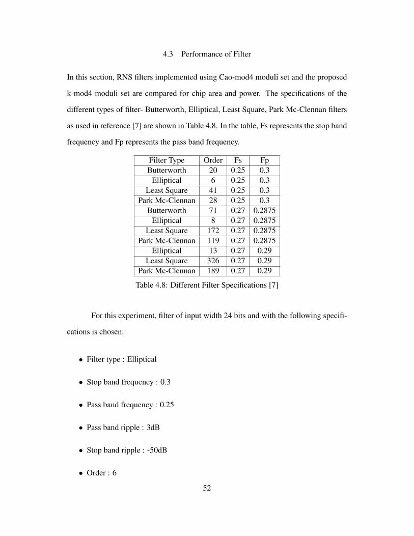
4.3 Performance of Filter
In this section, RNS filters implemented using Cao-mod4 moduli set and the proposed
k-mod4 moduli set are compared for chip area and power. The specifications of the
different types of filter- Butterworth, Elliptical, Least Square, Park Mc-Clennan filters
as used in reference [7] are shown in Table 4.8. In the table, Fs represents the stop band
frequency and Fp represents the pass band frequency.
Filter Type Order Fs FpButterworth 20 0.25 0.3
Elliptical 6 0.25 0.3Least Square 41 0.25 0.3
Park Mc-Clennan 28 0.25 0.3Butterworth 71 0.27 0.2875
Elliptical 8 0.27 0.2875Least Square 172 0.27 0.2875
Park Mc-Clennan 119 0.27 0.2875Elliptical 13 0.27 0.29
Least Square 326 0.27 0.29Park Mc-Clennan 189 0.27 0.29
Table 4.8: Different Filter Specifications [7]
For this experiment, filter of input width 24 bits and with the following specifi-
cations is chosen:
• Filter type : Elliptical
• Stop band frequency : 0.3
• Pass band frequency : 0.25
• Pass band ripple : 3dB
• Stop band ripple : -50dB
• Order : 6
52

The dynamic range of the filter with 24 bit input width and 6 taps is (2 ∗ 24+
log26)=51 bits. To implement this RNS filter of 51 bit dynamic range, using Cao-
mod4 moduli set, n = 14 has to be chosen according to the Table 4.2. Using the k-
mod4 moduli set, the parameters of n,k chosen to satisfy the required dynamic range
are n = 12 and k = 14 (from Table 4.2). Therefore the moduli sets chosen for Cao-
mod4 and k-mod4 are {214,214−1,214+1,215−1} and {214,212−1,212+1,213−1}
respectively.
Two filters using Cao-mod4 moduli set and k-mod4 moduli set are implemented
in RTL based on the RNS filter architecture as represented in Figure 3.1. The filters
implemented in verilog are simulated for functionality checking and synthesized under
no delay constraints. This analysis gives the total negative slack of the circuit which
denotes the minimum clock period required to synthesize the circuits. The following
table 4.9 shows the maximum frequency of operation and the cell area corresponding
to zero delay synthesis of the two filters.
Parameter Cao-mod4 k-mod4 %ImprovementGate count 13812 11279 18.3
Cell area(um2) 78829 64188 18.5Net area(um2) 61967 50025 19.2
Total area(um2) 140796 114213 18.8Delay (ns) 4.13 4.07 1.4
ADP (mm2*ns) 0.573 0.471 17.6
Table 4.9: Comparison of delay and area of k-mod4 and cao-mod4 filters
From the synthesis results, it can be seen that there is significant improvement
in cell area but the performance is comparable for both the designs. The synthesis tool
tries to improve the performance of the design boosting the circuit area to reduce the
total negative slack. Hence ADP is compared for the two designs which gives accurate
estimate of the performance for designs synthesized using zero delay.
After knowing the maximum frequency of operation, the two filters are synthe-
sized and placed and routed for the same clock frequency of 200Mhz. At this frequency,53

both the designs meet timing at post-synthesis as well as post-place and route levels.
Table 4.10 compares the post-place and route performance parameters of the two de-
signs.
Parameter Cao-mod4 k-mod4 %ImprovementGate count 20875 16485 21.0
Power(mW) 17.3 14.0 19.0Cell area(um2) 92870 74167 20.1
Chip Area(mm2) 0.20 0.16 20.6
Table 4.10: Area and Power improvements of k-mod4 moduli set
The reverse converter used in the filter designs are implemented as single stage
and two stage pipeline. The frequency of operation of the filters with single stage RC
is 344MHz and with two stage RC is 250MHz. Table 4.11 and Table 4.12 compare the
post-place and route performance parameters of the filters using single stage RC and
two stage RC.
Parameter Cao-mod4 k-mod4 %ImprovementGate count 21493 16857 21.5
Power(mW) 22.1 17.0 19.7Cell area(um2) 92364 73551 20.4
Chip Area(mm2) 0.155 0.124 19.4
Table 4.11: Comparison of filters with single stage RC
Parameter Cao-mod4 k-mod4 %ImprovementGate count 60079 46204 23.0
Power(mW) 31.8 23.5 26.1Cell area(um2) 93724 72079 23.1
Chip Area(mm2) 0.153 0.123 19.6
Table 4.12: Comparison of filters with two stage RC
The following figures Figure 4.7 and Figure 4.8 show the chip layouts of the
filters implemented using the Cao-mod4 moduli set and k-mod4 moduli set respectively
using two stage RC. The annotated values are the width and height of the chip. The
two filters are place and routed for the same initial densities and frequencies.54

The reduction in chip area and post-pnr power with the proposed moduli set is
20%. Power estimation was done using PrimeTime Px providing VCD (vector change
dump) file as input to estimate the realistic switching activities of the primary inputs
and internal nets.
55
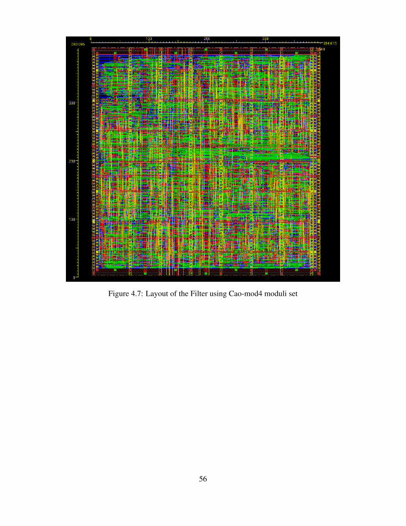
Figure 4.7: Layout of the Filter using Cao-mod4 moduli set
56

Figure 4.8: Layout of the Filter using k-mod4 moduli set
57

Chapter 5
Application of threshold logic
5.1 RC design using threshold logic
Reverse converter is the critical path unit in the filter. Pipelining is one alternative to
speed up the reverse conversion but it costs in additional registers. To speed up the
reverse conversion without sacrificing the power, it is implemented in threshold logic.
Threshold logic is an alternate logic style to CMOS that achieves better per-
formance with lower power. The standard cell in threshold logic in called threshold
logic latch (TLL). It is a clocked differential sense amplifier based circuit. TLL can
implement threshold functions up to fan in of 13. A threshold function is defined as a
boolean function y = f (x1,x2, · · · ,xn) if it can be represented as:
y =
1, ∑
n−1i=0 xiwi ≥ T,
0, otherwise(5.1)
where, wi is the weight of the input xi and T is the threshold. The circuit implementation
of threshold logic latch [16] is shown in figure 5.1. The critical aspect in designing a
circuit using TLL is identification of threshold functions in the circuit. The reverse
converter comprises of CSA and modulo adders. A CSA tree can be replaced by set
of counters. Counter function is a threshold function and can be implemented by few
TLL gates. In the two stage implementation of reverse converter, a 5-input CSA tree
feeding D flipflops shown in figure 5.2 is replaced by 5-input counter implemented
using threshold gates shown in figure 5.3. Here the logic depth of 3-FAs and DFF is
reduced to a single TLL gate depth. The delay of 6 XOR gates and the setup time of
DFF is replaced by setup time of a TLL gate. This absorption in logic depth results in
larger speed up at the cost of larger number of sequential gates.
The truth table of 5 bit counter is shown in table5.1. y2, y1, and y0 represent the
output of the 5-bit counter with number of 1’s in the input bits represented as Cnt.58
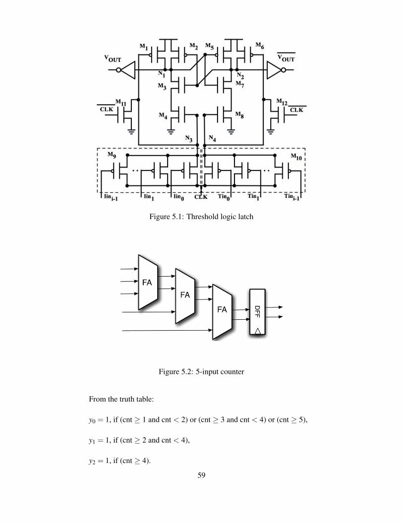
Figure 5.1: Threshold logic latch
Figure 5.2: 5-input counter
From the truth table:
y0 = 1, if (cnt ≥ 1 and cnt < 2) or (cnt ≥ 3 and cnt < 4) or (cnt ≥ 5),
y1 = 1, if (cnt ≥ 2 and cnt < 4),
y2 = 1, if (cnt ≥ 4).
59

TLL7
TLL5
TLL7
TLL9
TLL9
1 of 5
2 of 5
3 of 5
4 of 5
5 of 5
AND
AND
AND
ORX[4:0]
y2
y0
y1
Figure 5.3: 5-input TLL counter
y2 y1 y0 Cnt0 0 0 00 0 1 10 1 0 20 1 1 31 0 0 41 0 1 5
Table 5.1: Truth table of 5-input counter
The output of the TLL counter is in the form of three bits and it is reduced to
two bits using a CSA.
By identifying the 5-input counters in the reverse converter design, a hybrid
implementation of the two stage reverse converter is built using TLL and CMOS gates.
The CMOS and hybrid form of reverse converter of k-mod4 moduli set (n=8,k=10)
in two stage is implemented in RTL and place and routed. Figure 5.4 and figure 5.5
show the area and power improvements of the hybrid reverse converter at different
60
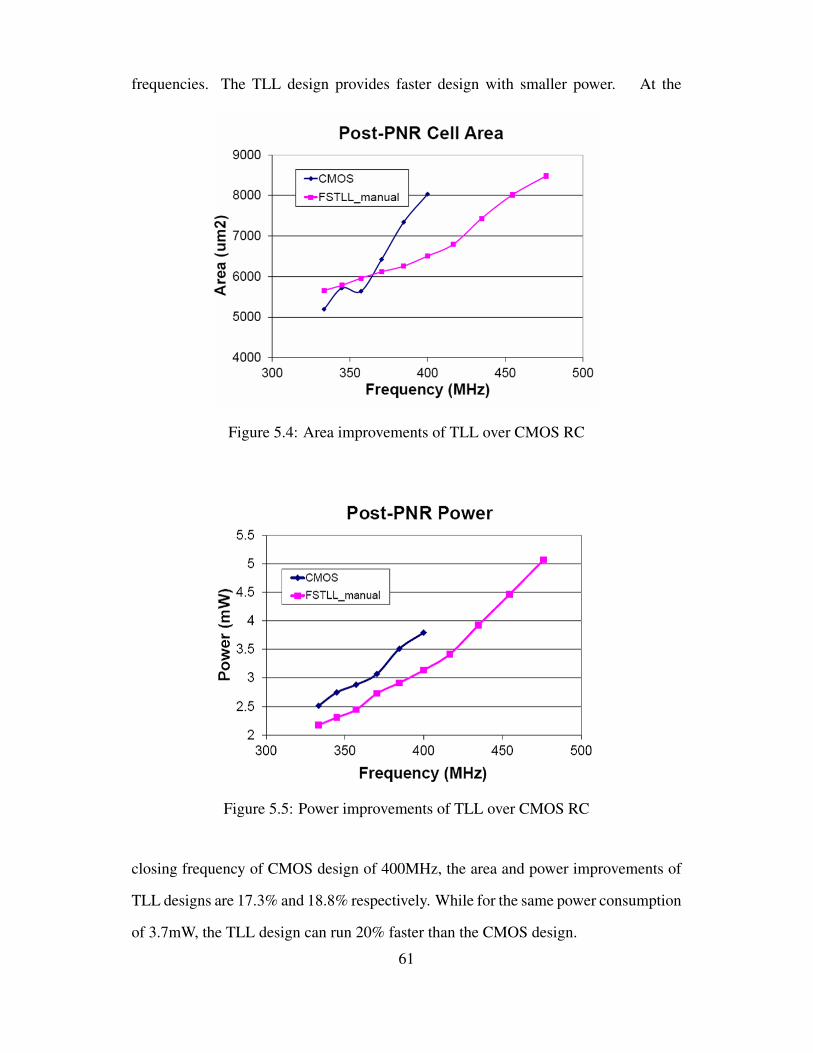
frequencies. The TLL design provides faster design with smaller power. At the
Figure 5.4: Area improvements of TLL over CMOS RC
Figure 5.5: Power improvements of TLL over CMOS RC
closing frequency of CMOS design of 400MHz, the area and power improvements of
TLL designs are 17.3% and 18.8% respectively. While for the same power consumption
of 3.7mW, the TLL design can run 20% faster than the CMOS design.
61

5.2 Experimental Setup
The EDA tools used in the experiments are listed below:
• Verilog Simulator : Cadence NCverilog
• Synthesis tool : Cadence RC
• Timing Analysis tool : Synopsys PrimeTime
• Place and Route tool : Cadence Encounter
• Static power analysis : Synopsys PrimeTime PX
62

Chapter 6
Conclusions
The thesis is a study of application of residue number system in the implementation of
FIR filters. The key contributions of the thesis are:
• It proposes a new RNS 4-moduli set for efficient implementation of FIR Filters
that addresses the drawbacks of existing 4-moduli sets. Compared to the exist-
ing 4-moduli sets, the proposed moduli set is more balanced, programmable for
various dynamic ranges and results in efficient distribution of computation load
among the RNS modulo channels.
• A reverse converter model has been derived based on mixed radix conversion
algorithm. The reverse converter model is CMOS implementation friendly. The
reverse converter circuit for the proposed moduli set outperformed the reverse
converter of state-of-the-art balanced moduli set both in terms of delay and area.
• MAC units implemented using the proposed moduli set and balanced 4-moduli
set in literature are synthesized and compared for power and cell area. Power
improvements of as much as 43% and cell area improvements of as much as 46%
are observed over various dynamic ranges.
• RNS FIR filters of 6-taps are implemented following the complete ASIC design
flow. The chip area and power are compared to demonstrate the advantages of
using the proposed RNS moduli set over the existing balanced moduli set.
• Proposed an application of new logic style to improve the speed of the reverse
converter. Using threshold logic, the reverse converter is sped up by 20% for the
same power.
63

REFERENCES
[1] B. Cao, C.H. Chang, and T. Srikanthan. An efficient reverse converter for 4-moduli set {2n−1,2n,2n+1,22n+1} based on new Chinese Remainder Theorem.IEEE Trans. Circuits Syst. I, Fundam. Theory Appl., 50:1296–1303, 2003.
[2] B. Cao, T. Srikantham, and C. H. Chang. Efficient reverse converters for four-moduli sets {2n− 1,2n,2n + 1,2n+1− 1} and {2n− 1,2n,2n + 1,2n−1− 1}. IEEProc. Comput. Digit. Tech., 152:687–696, 2005.
[3] R. Chaves and L. Sousa. {2n−1,2n+k,2n +1}: A New RNS Moduli Set Exten-sion. In Proc. DSD, pages 210–217, 2004.
[4] R. Chokshi, K.S. Berezowski, A. Shrivatsava, and S.J. Piestrak. Exploitingresidue number system for power-efficient digital signal processing in embeddedprocessors. In Proc. International Conference on Compilers, Architecture, andSynthesis for Embedded systems, pages 19–27, 2009.
[5] M. Re G.C. Cardarilli; A. Del Re; A. Nannarelli. Low Power and Low LeakageImplementation of RNS FIR Filters . In Thirty-Ninth Asilomar Conference onSignals, Systems and Computers, pages 1620–1624, 2005.
[6] A. Hiasat and H. S. Abdel-Aty-Zohdy. Residue-to-binary arithmetic converter forthe moduli set (2k,2k− 1,2k−1− 1). IEEE Trans. Circuits Syst. II, 45:204–208,1998.
[7] A. Hosangadi; F. Fallah; R. Kastner. Simultaneous optimization of delay andnumber of operations in multiplierless implementation of linear systems . In Proc.Int. Workshop Logic Synthesis, 2005.
[8] P.V.Ananda Mohan and A.B. Premkumar. RNS-to-Binary Converters for TwoFour-Moduli sets {2n−1,2n,2n +1,2n+1−1} and {2n−1,2n,2n +1,2n+1 +1}.IEEE Trans. Circuits Syst. I, 54(6):1245–1254, 2006.
[9] A.S. Molahosseini, K. Navi, C. Dadkhah, O. Kavehei, and S. Timarchi. EfficientReverse Converter Designs for the New 4-Moduli Sets {2n−1,2n,2n+1,22n+1−1} and {2n− 1,2n + 1,22n,22n + 1} Based on New CRTs. IEEE Trans. CircuitsSyst. I, 57:823–835, 2010.
[10] Alberto Nannarellli, Macro Re, and Gian Carlo Cardaralli. Tradeoffs BetweenResidue Number System and Traditional FIR Filters. In International Symposiumon Circuits and Systems, pages II305–II308, 2001.
64

[11] S.J. Piestrak. Design of residue generators and multioperand modulo adders usingcarry-save adders. IEEE Trans. Computers, 43:68–77, 1994.
[12] F. Pourbigharaz and H. M. Yassine. A signed-digit architecture for residue tobinary transformation. IEEE Trans. Comput, 46:1146–1150, 1997.
[13] A. B. Premkumar, E.L. Ang, and E. M.-K. Lai. A formal framework for conver-sion from binary to residue numbers. IEEE Trans. Circuits Syst. II:Analog andDigital Signal Processing, 49:135–144, 2002.
[14] A. B. Premkumar, E.L. Ang, and E. M.-K. Lai. Improved Memoryless RNSForward Converter Based on the Periodicity of Residues. IEEE Trans. CircuitsSyst. II, 53:133–137, 2006.
[15] B. Premkumar. An RNS to binary converter in 2n + 1; 2n; 2n 1 moduli set. IEEETrans. Circuits Syst. II, 39:480–482, 1992.
[16] X.Yao G.Chalivendra S. Patel S. Leshner, K.Berezowski and S.Vrudhula. A lowpower, high performance threshold logic-based standard cell multiplier in 65nmCMOS. In IEEE Symposium on VLSI (ISVLSI) 2010, 2010.
[17] Ming-Hwa Sheu, Su-Hon Lin, Yung-Tai Chen, and Yu-Chun Chang. High-Speedand Reduced-Area RNS Forward Converter Based on (2n−1,2n,2n+1). In Proc.APCCS, pages 821–824, 2004.
[18] M.A. Soderstrand, W.K. Jenkins, G.A. Jullien, and F.J. Taylor. Residue Num-ber System Arithmetic: Modern Applications in Digital Signal Processing. IEEEPress, Newyork, 1986.
[19] N Stamenkovi. Digital fir filter architecture based on the residue number system.Facta Universitatis - series : Architecture and Civil Engineering, 22:125, 2009.
[20] W. Wang, M. N. S. Swamy, M. O. Ahmad, and Y. Wang. A parallel residue-to-binary converter. In IEEE Inte. Conf. Acoustics, Speech, and Signal Processing,1999.
[21] Wei Wang, M.N.S Swamy, and M.O. Ahmad. Moduli Selection in RNS for Effi-cient VLSI Implementation. In International Symposium on Circuits and Systems,pages IV–512–IV–515, 2003.
65

[22] Yuke Wang. Residue-to-Binary converters based on new Chinese remaindertheourems. IEEE Trans. Circuits Syst. II:Analog and Digital Signal Processing,47:197–205, 2000.
[23] R. Zimmermann. Efficient VLSI Implementation of Modulo (2n + 1) Additionand Multiplication. In Proc. ISCA, pages 158–167, 1999.
66


![1JNXYZSLJS 0TSYFPY - physiopraxis.co.at · 5m^xntymjwfunj rns Ç 5m^xntymjwfunj rns Ç -fzxgjxzhm rns Ç -fzxgjxzhm rns Ç 9mjwfunj gjn zsx ns ijw 5wf]nx -fzxgjxzhmj nr zsi 'j_nwp](https://img.pdfslide.net/doc/110x75/5c49155e93f3c34c5506d276/1jnxyzsljs-0tsyfpy-5mxntymjwfunj-rns-c-5mxntymjwfunj-rns-c-fzxgjxzhm.jpg)