Embed Size (px)
Citation preview

A new sputtering device of radio-frequency magnetron discharge using a rectangularhollow-shaped electrodeYasunori Ohtsu, Yoshinobu Tsurume, and Hiroharu Fujita
Citation: Review of Scientific Instruments 69, 1833 (1998); doi: 10.1063/1.1148850 View online: http://dx.doi.org/10.1063/1.1148850 View Table of Contents: http://scitation.aip.org/content/aip/journal/rsi/69/4?ver=pdfcov Published by the AIP Publishing Articles you may be interested in Investigating the role of hydrogen in silicon deposition using an energy-resolved mass spectrometer and aLangmuir probe in an Ar/H2 radio frequency magnetron discharge Phys. Plasmas 19, 073521 (2012); 10.1063/1.4740508 Hollow target magnetron-sputter-type solid material ion sourcea) Rev. Sci. Instrum. 83, 02B715 (2012); 10.1063/1.3672474 High-power pulsed sputtering using a magnetron with enhanced plasma confinement J. Vac. Sci. Technol. A 25, 42 (2007); 10.1116/1.2388954 Shaped electrode and lens for a uniform radio-frequency capacitive plasma Appl. Phys. Lett. 82, 182 (2003); 10.1063/1.1534918 Growth and characterization of radio-frequency magnetron sputtered lead zirconate titanate thin films depositedon 111 Pt electrodes* J. Vac. Sci. Technol. A 16, 2876 (1998); 10.1116/1.581434
This article is copyrighted as indicated in the article. Reuse of AIP content is subject to the terms at: http://scitationnew.aip.org/termsconditions. Downloaded to IP:
67.180.227.126 On: Mon, 07 Apr 2014 05:44:46

REVIEW OF SCIENTIFIC INSTRUMENTS VOLUME 69, NUMBER 4 APRIL 1998
This art
A new sputtering device of radio-frequency magnetron dischargeusing a rectangular hollow-shaped electrode
Yasunori Ohtsu,a) Yoshinobu Tsurume, and Hiroharu FujitaDepartment of Electrical and Electronic Engineering, Saga University, Honjo-machi 1, Saga 840, Japan
~Received 2 June 1997; accepted for publication 19 January 1998!
A new sputtering device using a radio-frequency magnetron discharge with a rectangularhollow-shaped electrode has been developed for a low-pressure discharge~; a few mTorr!. Thespatial structures of the electron density, the etching rate of the target material~copper!, and thedeposition rate were measured in uniform and convex profiles of the externally applied magneticfield. The device realized the uniform use of the target material under the arrangement of themagnetic-field configuration. The resistivity of the deposited copper thin film was also obtained,which was found to be similar to that of conventional copper (;1028 V m). © 1998 AmericanInstitute of Physics.@S0034-6748~98!03304-8#
ss
en
smegneoc
nt-
edb
e
sup
alu
m
agesrofieb
and
eularw-
idth
ec-
e rfthe16of
pi-
asf 5
c-re-
s
ergne-.
al
ione,
sity,, re-rfas
I. INTRODUCTION
Recently, physical sputtering1–3 and reactivesputtering4–6 methods were widely used for material proceing. Especially, dc and/or radio-frequency~rf! planar magne-tron discharge plasmas7–10 were applied to perform a highplasma density and a high deposition rate. However, thplasma sources have been difficult to perform uniform aefficient use of target materials because the profile of pladensity is nonuniform owing to the use of the ring-shappermanent magnet. More effective and uniform use of tarmaterials has been required, especially for expensive oSeveral types of plasma sources11–16 have been proposed tachieve these requirements. Plasma sources such as elecyclotron resonance~ECR! microwave plasma and helicowave excited plasma17,18 have also been proposed for sputering devices available for low-pressure gas~a few mTorr!.Since these plasma sources are very expensive comparthe conventional magnetron discharge device, it mightdifficult to adopt them directly in industry.
Conventional magnetron discharge devices have bprepared at a pressure (<10 mTorr) higher than that in ECRmicrowave plasma devices. On the other hand, low-presplasma sources are necessary so that the ions mean-freeis large and they are not scattered in the sheath. It isnecessary to produce a high-quality thin film without imprities.
In this paper, we present a type of rf magnetron plassource in a low-pressure gas~; a few mTorr!, which wasmodified from our previous plasma device15 to a bigger rect-angular hollow-shaped copper electrode. The results hsuccessfully provided a uniform etching rate of the tarmaterial ~copper! and the preparation of copper thin filmwith a large diameter and an effective resistivity. Spatial pfiles of the plasma parameters in the device were clariusing a movable Langmuir probe. The copper thin films o
a!Electronic mail: [email protected]
1830034-6748/98/69(4)/1833/4/$15.00
icle is copyrighted as indicated in the article. Reuse of AIP content is subje
67.180.227.126 On: Mon,
-
seda
dets.
tron
toe
en
reath
so-
a
vet
-d-
tained by our device were valued on the deposition ratethe resistivity.
II. EXPERIMENTAL APPARATUS
Figures 1~a! and 1~b! show a schematic diagram of thexperimental apparatus and the construction of a rectanghollow-shaped rf electrode, respectively. The copper holloshaped rf electrode has a cross section of 110 mm in w~r axis! and 55 mm in height~h axis!, and a length~z axis! of120 mm as shown in Fig. 1~b!. A rf ~13.56 MHz! powersupply was applied to the rf electrode. Outside the rf eltrode, a grounded electrode was installed with a 2 mminsu-lator to suppress the discharge on the outer surface of thelectrode. The hollow-shaped rf electrode covered withgrounded electrode was placed in a cylindrical chambercm in diameter and 110 cm in length, where various typesmagnetic-flux density profiles were externally applied. Tycal profiles are as shown in Fig. 1~b!, where the maximumvalue of magnetic-flux density is about 300 G. Argon gwas introduced to the chamber at a fixed pressure omTorr. Since the axially applied magnetic-fieldB andelectric-fieldE created by the sheath formation of the rf eletrode were parallel and perpendicular to the rf electrode,spectively, anE3B drift motion of charged particles waproduced in the direction perpendicular toE andB. Thus, theE3B drift motion was in a closed path around the innsurface of the rf electrode, and a rectangular-shaped matron discharge was realized to confine electrons and ions
A cylindrical Langmuir probe~tungsten wire: 0.1 mm indiameter and 2 mm in length! used to measure the spatiprofiles of the plasma parameters was movable inr and zaxes at a fixed heighth50 cm@see Fig. 1~a!#. Spatial profilesof the plasma density were estimated from ion saturatcurrent I is collected by a highly negatively biased probwhereI is'0.6enAkTe /mi .
19 Here,e, n, k, Te , andmi de-noted the charge magnitude of electrons, plasma denBoltzmann constant, electron temperature, and ion massspectively. In order to examine the etching rate of theelectrode surface, a copper plate with a width of 1 mm w
3 © 1998 American Institute of Physics
ct to the terms at: http://scitationnew.aip.org/termsconditions. Downloaded to IP:
07 Apr 2014 05:44:46
igce
e
o
ththhd
ta
filee
neat
ro
x
oftheb-maxi-
ere
ci-ethe
er-
sitionl
er
1834 Rev. Sci. Instrum., Vol. 69, No. 4, April 1998 Ohtsu, Tsurume, and Fujita
This art
placed on the bottom of the rf electrode as shown in F1~b!. The substrate deposited copper thin films were plaon r –z plane ath50 cm.
III. RESULTS AND DISCUSSION
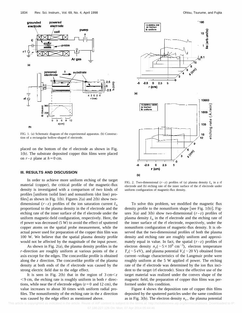
In order to achieve more uniform etching of the targmaterial ~copper!, the critical profile of the magnetic-fluxdensity is investigated with a comparison of two kindsprofiles @uniform ~solid line! and nonuniform~dot line! pro-files# as shown in Fig. 1~b!. Figures 2~a! and 2~b! show two-dimensional (r –z) profiles of the ion saturation currentI is
proportional to the plasma density in the rf electrode andetching rate of the inner surface of the rf electrode underuniform magnetic-field configuration, respectively. Here, trf power was decreased~5 W! to avoid the effect of sputterecopper atoms on the spatial probe measurement, whileactual power used for preparation of the copper thin film w100 W. We believe that the spatial plasma density prowould not be affected by the magnitude of the input pow
As shown in Fig. 2~a!, the plasma density profiles in thr -direction are roughly uniform at various points of thezaxis except for the edges. The concavelike profile is obtaialong thez direction. The concavelike profile of the plasmdensity at both ends of the rf electrode was caused bystrong electric field due to the edge effect.
It is seen in Fig. 2~b! that in the region of 3 cm,z,9 cm, the etching rate is roughly uniform in bothr direc-tions, while near the rf electrode edges~z50 and 12 cm!, thevalue increases to about 30 times with uniform radial pfiles. The nonuniformity of the etching rate in thez directionwas caused by the edge effect as mentioned above.
FIG. 1. ~a! Schematic diagram of the experimental apparatus.~b! Construc-tion of a rectangular hollow-shaped rf electrode.
icle is copyrighted as indicated in the article. Reuse of AIP content is subje
67.180.227.126 On: Mon,
.d
t
f
ee
e
heser.
d
he
-
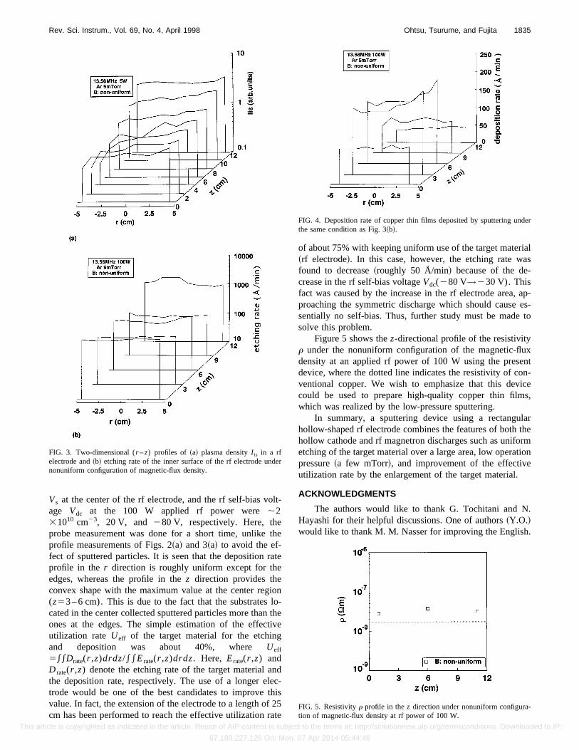
To solve this problem, we modified the magnetic fludensity profile to the nonuniform shape@see Fig. 1~b!#. Fig-ures 3~a! and 3~b! show two-dimensional (r –z) profiles ofplasma densityI is in the rf electrode and the etching ratethe inner surface of the rf electrode, respectively, undernonuniform configuration of magnetic-flux density. It is oserved that the two-dimensional profiles of both the plasdensity and etching rate are roughly uniform and appromately equal in value. In fact, the spatial (r –z) profiles ofelectron densityne(;53109 cm23), electron temperatureTe(;5 eV), and plasma potentialVs(;20 V) obtained fromcurrent–voltage characteristics of the Langmuir probe wroughly uniform at the 5 W applied rf power. The etchingrate of the rf electrode was determined by the ion flux indent to the target~rf electrode!. Since the effective use of thtarget material was realized under the convex shape ofmagnetic field, the preparation of copper thin films was pformed under this condition.
Figure 4 shows the deposition rate of copper thin filmdeposited by the sputtered particles under the same condas in Fig. 3~b!. The electron densityne , the plasma potentia
FIG. 2. Two-dimensional (r –z) profiles of ~a! plasma densityI is in a rfelectrode and~b! etching rate of the inner surface of the rf electrode unduniform configuration of magnetic-flux density.
ct to the terms at: http://scitationnew.aip.org/termsconditions. Downloaded to IP:
07 Apr 2014 05:44:46
lt
th
rae
iolot
tivg
nleth2
ra
rialas-
, ap-es-to
uxentn-ices,
larthe
ormtion
.
.
de
der
-
1835Rev. Sci. Instrum., Vol. 69, No. 4, April 1998 Ohtsu, Tsurume, and Fujita
This art
Vs at the center of the rf electrode, and the rf self-bias voage Vdc at the 100 W applied rf power were;231010 cm23, 20 V, and 280 V, respectively. Here, theprobe measurement was done for a short time, unlikeprofile measurements of Figs. 2~a! and 3~a! to avoid the ef-fect of sputtered particles. It is seen that the depositionprofile in the r direction is roughly uniform except for thedges, whereas the profile in thez direction provides theconvex shape with the maximum value at the center reg(z53 – 6 cm). This is due to the fact that the substratescated in the center collected sputtered particles more thanones at the edges. The simple estimation of the effecutilization rate Ueff of the target material for the etchinand deposition was about 40%, whereUeff
5**Drate(r ,z)drdz/**Erate(r ,z)drdz. Here, Erate(r ,z) andD rate(r ,z) denote the etching rate of the target material athe deposition rate, respectively. The use of a longer etrode would be one of the best candidates to improvevalue. In fact, the extension of the electrode to a length ofcm has been performed to reach the effective utilization
FIG. 3. Two-dimensional (r –z) profiles of ~a! plasma densityI is in a rfelectrode and~b! etching rate of the inner surface of the rf electrode unnonuniform configuration of magnetic-flux density.
icle is copyrighted as indicated in the article. Reuse of AIP content is subje
67.180.227.126 On: Mon,
-
e
te
n-hee
dc-is5te
of about 75% with keeping uniform use of the target mate~rf electrode!. In this case, however, the etching rate wfound to decrease~roughly 50 Å/min! because of the decrease in the rf self-bias voltageVdc(280 V→230 V). Thisfact was caused by the increase in the rf electrode areaproaching the symmetric discharge which should causesentially no self-bias. Thus, further study must be madesolve this problem.
Figure 5 shows thez-directional profile of the resistivityr under the nonuniform configuration of the magnetic-fldensity at an applied rf power of 100 W using the presdevice, where the dotted line indicates the resistivity of coventional copper. We wish to emphasize that this devcould be used to prepare high-quality copper thin filmwhich was realized by the low-pressure sputtering.
In summary, a sputtering device using a rectanguhollow-shaped rf electrode combines the features of bothhollow cathode and rf magnetron discharges such as unifetching of the target material over a large area, low operapressure~a few mTorr!, and improvement of the effectiveutilization rate by the enlargement of the target material.
ACKNOWLEDGMENTS
The authors would like to thank G. Tochitani and NHayashi for their helpful discussions. One of authors~Y.O.!would like to thank M. M. Nasser for improving the English
r
FIG. 4. Deposition rate of copper thin films deposited by sputtering unthe same condition as Fig. 3~b!.
FIG. 5. Resistivityr profile in thez direction under nonuniform configuration of magnetic-flux density at rf power of 100 W.
ct to the terms at: http://scitationnew.aip.org/termsconditions. Downloaded to IP:
07 Apr 2014 05:44:46

c
,
n
A
au-7th317
ch-
S.
1836 Rev. Sci. Instrum., Vol. 69, No. 4, April 1998 Ohtsu, Tsurume, and Fujita
This art
1H. F. Winters and J. W. Coburn, Surf. Sci. Rep.14, 161 ~1992!.2J. A. Thornton, J. Vac. Sci. Technol. A4, 3059~1986!.3M. Konuma, Film Deposition by Plasma Techniques~Springer, NewYork, 1992!.
4S. Berg, H. O. Blom, M. Moradi, C. Nender, and T. Larsson, J. Vac. STechnol. A7, 1225~1989!.
5K. E. Davies, M. Gross, and C. M. Horwitz, J. Vac. Sci. Technol. A11,2752 ~1993!.
6L. H-Chul, K. G-Hong, H. S-Ku, L. K-Young, Y. Y-Joong, C. C-Hwauand L. J-Young, Thin Solid Films261, 148 ~1995!.
7J. A. Thornton and A. S. Penfold, inThin Film Processes, edited by J. L.Vossen and W. Kern~Academic, New York, 1978!.
8R. K. Waits, inThin Film Processes, edited by J. L. Vossen and W. Ker~Academic, New York, 1978!.
9A. E. Wendt and M. A. Lieberman, J. Vac. Sci. Technol. A8, 902~1990!.
icle is copyrighted as indicated in the article. Reuse of AIP content is subje
67.180.227.126 On: Mon,
i.
10T. E. Sheindan, M. J. Goeckner, and J. Goree, J. Vac. Sci. Technol.9,688 ~1990!.
11X. Quyang, A. H. Kitai, and T. Xiao, J. Appl. Phys.79, 3229~1996!.12J. Uramoto, Research Report of IPP, Nagoya University IPPJ-628~1983!.13R. Azuma, K. Nanri, S. Harakawa, H. Watanabe, T. Noguchi, K. Yam
chi, K. Sunako, T. Takikawa, and K. Takayama, in Proceedings of theSymposium on Plasma Processing, edited by I. Kato and R. Itatani,~The Japan Society of Applied Physics, 1990!.
14Y. Okuno, H. Ishikura, and H. Fujita, Rev. Sci. Instrum.63, 44 ~1992!.15Y. Okuno, H. Ishikura, and H. Fujita, Rev. Sci. Instrum.63, 3725~1992!.16K. Murata, Y. Okuno, and H. Fujita, Rev. Sci. Instrum.65, 673 ~1994!.17J. Q. Zhang, Y. Setsuhara, T. Ariyasu, and S. Miyake, J. Vac. Sci. Te
nol. A 4, 2163~1996!.18Y. Ohtsu, G. Tochitani, H. Fujita, J. Q. Zhang, Y. Setsuhara, and
Miyake, Jpn. J. Appl. Phys., Part 136, 4620~1997!.19F. F. Chen, inPlasma Diagnostic Techniques, edited by R. H. Huddle-
stone and S. L. Leonard~Academic, New York, 1965!.
ct to the terms at: http://scitationnew.aip.org/termsconditions. Downloaded to IP:
07 Apr 2014 05:44:46


![[PPT]Home-Made DC Magnetron Sputtering System - …faculty.kfupm.edu.sa/.../research_files/magnetron.ppt · Web viewHome-Made DC Magnetron Sputtering System Chamber and Gas supply](https://img.pdfslide.net/doc/110x75/5aa9b1b37f8b9a90188d2f45/ppthome-made-dc-magnetron-sputtering-system-viewhome-made-dc-magnetron-sputtering.jpg)