Embed Size (px)
Citation preview
Progress In Electromagnetics Research C, Vol. 68, 153–161, 2016
A Novel Low RCS Microstrip Antenna Array Using Thinand Wideband Radar Absorbing Structure Based
on Embedded Passives Resistors
Madhu A. Ramkumar1, Chandrika Sudhendra1, *, and Kark Rao2
Abstract—A novel low radar cross section (RCS) microstrip patch antenna array (1× 4) (MSPAA) isreported in this paper. A thin and wideband radar absorber (RA) based on a single octagonal loop (SOL)resistive frequency selective surface (FSS) is designed for realizing out-of-band RCS reduction of theMSPAA from 6.2 GHz to 18 GHz. The RA is designed for −15 dB reflectivity from 6.2 GHz to 18 GHz.Embedded Passives (EP) resistors are used for implementing the resistors as integral to the substratewith no soldering at all which results in a quantum improvement in reliability. Full wave analysis ofthe low RCS MSPAA with the RA is carried out using HFSS. RCS measurements are performed, andan RCS reduction of 6 to 18 dB is attained compared to the reference antenna array over a wide bandfrom 6 GHz to 18 GHz, with no degradation in VSWR and gain of the antenna array. The thin andwideband RA with its low weight and flight worthy constituent materials can be applied independentlyas skins of a stealthy UAV configured primarily for low RCS with external shaping, and the proposedantenna array can be used without modifications, as a low RCS conformal antenna structure.
1. INTRODUCTION
Microstrip antennas on board an air vehicle platform designed primarily for stealth contributesignificantly to the overall radar cross section (RCS). Design of a low observable platform for realizingradar stealth includes the primary external shape design for monostatic radar cross section reduction(RCSR) and application of radar absorbers [1–7] which need to be designed and integrated as robustload bearing radar absorbing structures (RAS). Radar absorbers such as Salisbury screen [1], JaumannRA [2–4] and different types of circuit analog absorbers [5–7] have been reported in open literature forrealizing RCSR.
Antenna RCS [8] is defined as
σ =∣∣√
σs−(1−ΓA)√
σreiϕ
∣∣2
(1)
where, σ is the total RCS of the target, σs related to the field scattered by the short-circuited antenna,σr the field scattered by the antenna that involves value of the port impedance, ΓA the antenna reflectioncoefficient, and ϕ the relative phase between the two terms. Hence, RCS is the difference between twoterms, one being the square root of a complex “structural” cross section and the other (1 − Γ) timesthe square root of a complex “antenna” cross section.
Frequency selective surfaces (FSS) have been used in the ground plane as bandpass filters [9, 10],resulting in narrow out-of-band RCSR of the microstrip antenna, and band stop filters [11–13], otherfor achieving wide-band RCSR in out-of-band frequency regions of the antenna. Polarization dependent
Received 5 August 2016, Accepted 21 September 2016, Scheduled 18 October 2016* Corresponding author: Chandrika Sudhendra ([email protected]).1 Aeronautical Development Establishment (ADE), Ministry of Defence, DRDO Bengaluru, India. 2 PES College of Engineering,Mandya, Karnataka, India.
154 Ramkumar, Sudhendra, and Rao
FSS in the modified ground plane (MGP) for wide angle, in-band RCSR is reported in [14]. Fractaluniplanar compact ground is proposed in [15] for out-of-band structural RCSR. As low RCS antennasare a primary requirement of stealthy aircrafts/UCAVs, the FSS structures in the ground plane of anantenna on board a stealthy air vehicle loses its basic FSS characteristics attributed to unavailability offree space environment to the ground plane. This would result in degraded RCSR. Narrow-band, wide-band, dual-band, in-band and out-of-band RCSR of antenna, with either lower or increased gain usingmeta surfaces comprising EBG, AMC, lumped element loaded FSS is reported in [16–22] which resultsin either increased real estate of the antenna or the profile which would increase the aerodynamic dragon a stealthy air vehicle, limiting the application. Lumped element loading is used for realizing antennaRCSR in [16, 18, 19, 22, 23]. However, lumped resistors’ loading is highly susceptible to soldering relateddefects and result in reduced reliability.
In this paper, RCSR of a microstrip patch antenna array (MSPAA) is described using a singleoctagonal loop resistive FSS based radar absorber. The novelty of the paper lies in the implementation ofthe low RCS MSPAA with absorber using embedded passives (EP) resistors, as a first time developmentin low RCS microstrip antennas, in open literature. The EP resistors are an enabling technology forimplementing the resistive FSS layer of radar absorber for realizing the low RCS antenna as large numberof resistors can be embedded without soldering, thus eliminating soldering related defects, reduced crosstalk and parasitic reactance. RA design with full wave analysis using HFSS is described in the firstsection, and low RCS (1 × 4) MSPAA design is described next, followed by the design, simulation,fabrication and RCS measurements of the low RCS MSPAA. The RA is designed for reflectivity of−15 dB over 6.2 GHz to 16 GHz frequency bands and is realized as a thin and wideband Radar Absorbingstructure (RAS). The low RCS antenna realized using the RA finds direct applications on any stealthdesign driven platform as a conformal stealthy structure where stealth design features such as externalshaping and RA are already in place.
2. EM DESIGN AND FULL WAVE ANALYSIS OF RESISTIVE OCTAGONAL LOOPFSS ELEMENT BASED RADAR ABSORBER
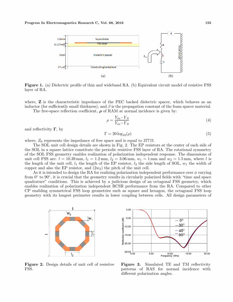
The dielectric profile of the thin and wideband radar absorber (RA) shown in Fig. 1(a) comprises asuperstrate top layer with the resistive FSS layer underneath, separated from the conducting groundplane by an RF transparent dielectric spacer. The superstrate layer is a 1.6 mm thick Rogers Ultralam2000, with εr = 2.5 and tan δ = 0.0019. The crucial resistive FSS layer is conceptualized and designedusing single octagonal loop (SOL) FSS geometry with resistors at the center of each side of the loop andis developed as a PCB using a 5mils thick FR4 substrate. The resistors crucial for providing resistiveloss are designed and implemented as EP resistors using a commercially available 50 Ω/sq resistive sheet.
The total thickness of RA proposed in this paper is 5.6 mm (including superstrate thickness of1.6 mm and dielectric spacer Rohacel foam thickness of 4 mm with εr = 1.07 and tan δ = 0.0007) usedas the spacer between the resistive FSS layer and the conducting backplane and hence does not violatethe fundamental minimum thickness constraint given by Rozanov in [24]. The design of RA lies inimplementation of large number of resistors as EP resistors. The RA is modeled using transmissionline (TL) equivalent circuit model and is given in Fig. 1(b). The resistive FSS layer is modeled as aseries RLC circuit in shunt with the dielectric spacer backed conducting ground plane, acting as a shortcircuited transmission with length <λ/4(d), (where λ is the operating wavelength at the design centerfrequency, 11.75 GHz), and the grounded dielectric spacer terminated in short circuit is modeled as anequivalent inductance.
The surface impedance of FSS layer is given by:
ZFSS = RS +1
jωC+ jωL (2)
where, R is the surface resistance, C the capacitance and L the surface inductance of the FSS layer.The free-space input impedance of RAM for normal incidence is given by:
Zin =jZFSSZ tan(βd)
(ZFSS + jZ tan(βd))(3)
Progress In Electromagnetics Research C, Vol. 68, 2016 155
(a) (b)
Figure 1. (a) Dielectric profile of thin and wideband RA. (b) Equivalent circuit model of resistive FSSlayer of RA.
where, Z is the characteristic impedance of the PEC backed dielectric spacer, which behaves as aninductor (for sufficiently small thickness), and β is the propagation constant of the foam spacer material.
The free-space reflection coefficient, ρ of RAM at normal incidence is given by:
ρ =Yin−Y 0
Yin−Y 0(4)
and reflectivity Γ, byΓ = 20 log10(ρ) (5)
where, Z0 represents the impedance of free space and is equal to 377 Ω.The SOL unit cell design details are shown in Fig. 2. The EP resistors at the center of each side of
the SOL in a square lattice constitute the periodic resistive FSS layer of RA. The rotational symmetryof the SOL FSS geometry enables realization of polarization independent response. The dimensions ofunit cell FSS are: l = 10.39 mm, l1 = 1.2 mm, l2 = 3.06 mm, w1 = 1 mm and w2 = 1.5 mm, where l isthe length of the unit cell, l1 the length of the EP resistor, l2 the side length of SOL, w1 the width ofcopper and also the EP resistor, and (2w2) the pitch of the unit cell.
As it is intended to design the RA for realizing polarization independent performance over φ varyingfrom 0◦ to 90◦, it is crucial that the geometry results in circularly polarized fields with “time and spacequadrature” conditions. This is achieved by a judicious design of an octagonal FSS geometry, whichenables realization of polarization independent RCSR performance from the RA. Compared to otherCP enabling symmetrical FSS loop geometries such as square and hexagon, the octagonal FSS loopgeometry with its longest perimeter results in lower coupling between cells. All design parameters of
Figure 2. Design details of unit cell of resistiveFSS.
Figure 3. Simulated TE and TM reflectivitypatterns of RAS for normal incidence withdifferent polarization angles.

156 Ramkumar, Sudhendra, and Rao
(a) (b)
Figure 4. Reflectivity performance of RA with various angle of incidence. (a) TE incidence. (b) TMincidence.
the unit cell geometry are extracted using GA optimization in HFSS, with constraints in thickness forrealizing the desired wideband RCSR performance.
A graph of optimized reflectivity performance vs. frequency is plotted in Fig. 3, for normal incidence.It is observed from the plot that a reflectivity/S11 of −10 dB (minimum) can be realized from 5.5 GHzto 18 GHz for both TE and TM incidences and indicates polarization independent performance of RA.Next, the RCSR performance of RA for non-normal angles of incidence is studied. Figs. 4(a) and 4(b)show the TM and TE performances of RA from 0◦ to 30◦. It is observed from the figures that the−10 dB reflectivity performance of RA is preserved for angles of incidence up to 30◦.
3. DESIGN AND FULL WAVE ANALYSIS OF LOW RCS MICROSTRIP ANTENNAARRAY
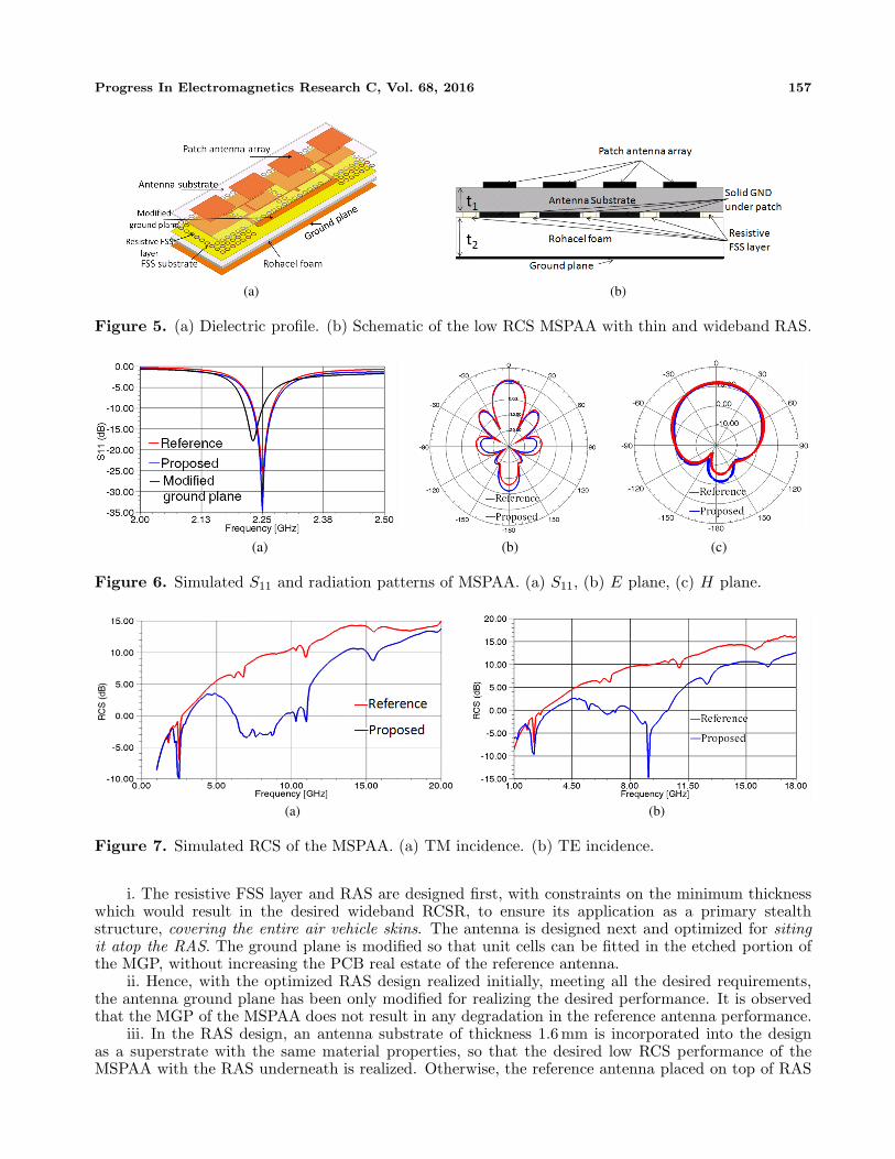
A reference (1×4) element microstrip antenna array (MSPAA) for telemetry applications is designed at2.25 GHz using an RT Duroid microwave substrate of size (300×98.75) mm2, with relative permittivity,εr = 2.5, tan δ = 0.0019 and thickness 1.6 mm. The dielectric profile of the low RCS MSPAA is shownin Fig. 5(a), and the schematic is shown in Fig. 5(b). The modified ground plane (MGP) of the referenceMSPAA comprises solid copper ground underneath the patches and the feed lines only. The remainingarea of the MGP layer is filled with octagonal resistive FSS elements, realized as a 5mils thick FR4PCB, referred to as the resistive FSS layer in the earlier section. The resistive FSS layer is spacedfrom the conducting ground plane by the RF transparent Rohacel foam layer of thickness 4 mm withεr = 1.07 and tan δ = 0.0007. A thin tin-plated 3M copper foil is used as ground plane of the proposedlow RCS MSPAA. The proposed low RCS antenna design is optimized in HFSS for realizing the desiredperformance, and the simulated S11 of the reference and proposed antenna are plotted in Fig. 6(a). Thereference MSPAA is designed for a center frequency of 2.25 GHz with a bandwidth of 39 MHz. It isnoted that with MGP, the center frequency shifts from 2.25 GHz to 2.23 GHz as shown in Fig. 6(a). Byfilling the resistive FSS elements around the MGP, the desired center frequency of 2.25 GHz is retrievedas the FSS elements act as PEC at 2.25 GHz, and the bandwidth of the proposed low RCS MSPAA is43 MHz. The simulated gains of the reference and proposed low RCS MSPAA are 12 dBi in both E andH-planes, as shown in Figs. 6(b) and 6(c). It is observed that the proposed low RCS MSPAA can berealized with no degradation in gain. A very marginal increase in the back lobe is observed, and someside lobes are reduced.
Next, the structural RCS of the MSPAA is simulated in HFSS, and the results are plotted inFigs. 7(a) and (b). It is observed from the superposed plots that a 5 dB to 14 dB reduction in RCS isobserved over a frequency range of 6 GHz to 18 GHz for both TE and TM incidences.
From the simulated radiation performance plots, it is observed that there is no degradation in gain,and the two graphs coincide.
The design of the low RCS MSPAA is optimized with the following considerations:
Progress In Electromagnetics Research C, Vol. 68, 2016 157
(a) (b)
Figure 5. (a) Dielectric profile. (b) Schematic of the low RCS MSPAA with thin and wideband RAS.
(a) (b) (c)
Figure 6. Simulated S11 and radiation patterns of MSPAA. (a) S11, (b) E plane, (c) H plane.
(a) (b)
Figure 7. Simulated RCS of the MSPAA. (a) TM incidence. (b) TE incidence.
i. The resistive FSS layer and RAS are designed first, with constraints on the minimum thicknesswhich would result in the desired wideband RCSR, to ensure its application as a primary stealthstructure, covering the entire air vehicle skins. The antenna is designed next and optimized for sitingit atop the RAS. The ground plane is modified so that unit cells can be fitted in the etched portion ofthe MGP, without increasing the PCB real estate of the reference antenna.
ii. Hence, with the optimized RAS design realized initially, meeting all the desired requirements,the antenna ground plane has been only modified for realizing the desired performance. It is observedthat the MGP of the MSPAA does not result in any degradation in the reference antenna performance.
iii. In the RAS design, an antenna substrate of thickness 1.6 mm is incorporated into the designas a superstrate with the same material properties, so that the desired low RCS performance of theMSPAA with the RAS underneath is realized. Otherwise, the reference antenna placed on top of RAS
158 Ramkumar, Sudhendra, and Rao
would not be expected to perform as desired.iv. The modified ground plane of the proposed MSPAA, comprising solid ground beneath the
patches and the feed lines yields the intended performance of the MSPAA without deteriorating eitherthe impedance matching or the radiation performance of the antenna.
v. The resistive FSS layer, which is based on SOL FSS geometry with integral resistors, results insignificant improvement in reliability, with no increase in the PCB real estate, thus rendering the designapplication worthy on any stealth platform.
vi. The radar absorber, designed and implemented as a thin and wideband radar absorbingstructure, can be used independently as structural RAS and as skins of a stealthy UAV, and thelow RCS conformal antenna can be seamlessly integrated into the skin with no protuberances ormodifications to the existing stealth design with primary external shaping. Also, the Rohacel foambeing a closed cell, flight worthy, low loss material can be used as the dielectric spacer with the requiredstructural properties. It is observed that the RA design and implementation on any stealth platformdemands multi-disciplinary inputs from structures and materials. The conducting ground plane of theRA can be easily replaced by using carbon fiber reinforced plastic (CFRP) with absolutely no loss inRCS performance of the conducting back plane and better structural characteristics. Monostatic RCSexperiments performed earlier on similar size CFRP and Aluminium panels in a compact RCS testrange showed that the RCS of CFRP and aluminium panels were matching both in amplitude andangle differing to the tune of 0.2 dB. The superstrate could be designed using glass fiber reinforcedplastic (GFRP) meeting the required structural strength and also radar transparency, while meetingall RCSR requirements of RAS. Hence, the thin and wideband RAS can be used as a multi-functionalUAV structure while satisfying stealth characteristics.
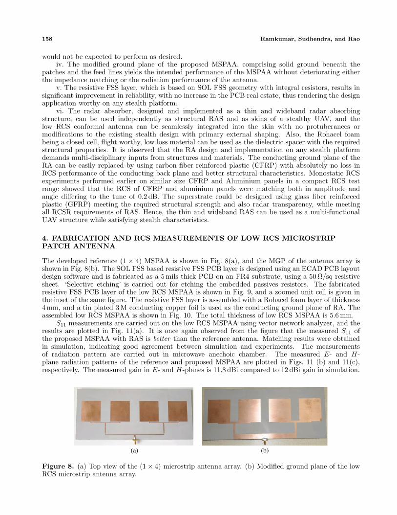
4. FABRICATION AND RCS MEASUREMENTS OF LOW RCS MICROSTRIPPATCH ANTENNA
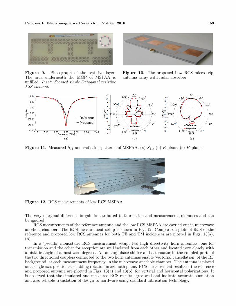
The developed reference (1 × 4) MSPAA is shown in Fig. 8(a), and the MGP of the antenna array isshown in Fig. 8(b). The SOL FSS based resistive FSS PCB layer is designed using an ECAD PCB layoutdesign software and is fabricated as a 5mils thick PCB on an FR4 substrate, using a 50 Ω/sq resistivesheet. ‘Selective etching’ is carried out for etching the embedded passives resistors. The fabricatedresistive FSS PCB layer of the low RCS MSPAA is shown in Fig. 9, and a zoomed unit cell is given inthe inset of the same figure. The resistive FSS layer is assembled with a Rohacel foam layer of thickness4mm, and a tin plated 3M conducting copper foil is used as the conducting ground plane of RA. Theassembled low RCS MSPAA is shown in Fig. 10. The total thickness of low RCS MSPAA is 5.6 mm.
S11 measurements are carried out on the low RCS MSPAA using vector network analyzer, and theresults are plotted in Fig. 11(a). It is once again observed from the figure that the measured S11 ofthe proposed MSPAA with RAS is better than the reference antenna. Matching results were obtainedin simulation, indicating good agreement between simulation and experiments. The measurementsof radiation pattern are carried out in microwave anechoic chamber. The measured E- and H-plane radiation patterns of the reference and proposed MSPAA are plotted in Figs. 11 (b) and 11(c),respectively. The measured gain in E- and H-planes is 11.8 dBi compared to 12 dBi gain in simulation.
(a) (b)
Figure 8. (a) Top view of the (1 × 4) microstrip antenna array. (b) Modified ground plane of the lowRCS microstrip antenna array.
Progress In Electromagnetics Research C, Vol. 68, 2016 159
Figure 9. Photograph of the resistive layer.The area underneath the MGP of MSPAA isunfilled. Inset: Zoomed single Octagonal resistiveFSS element.
Figure 10. The proposed Low RCS microstripantenna array with radar absorber.
(a) (c)(b)
Figure 11. Measured S11 and radiation patterns of MSPAA. (a) S11, (b) E plane, (c) H plane.
Figure 12. RCS measurements of low RCS MSPAA.
The very marginal difference in gain is attributed to fabrication and measurement tolerances and canbe ignored.
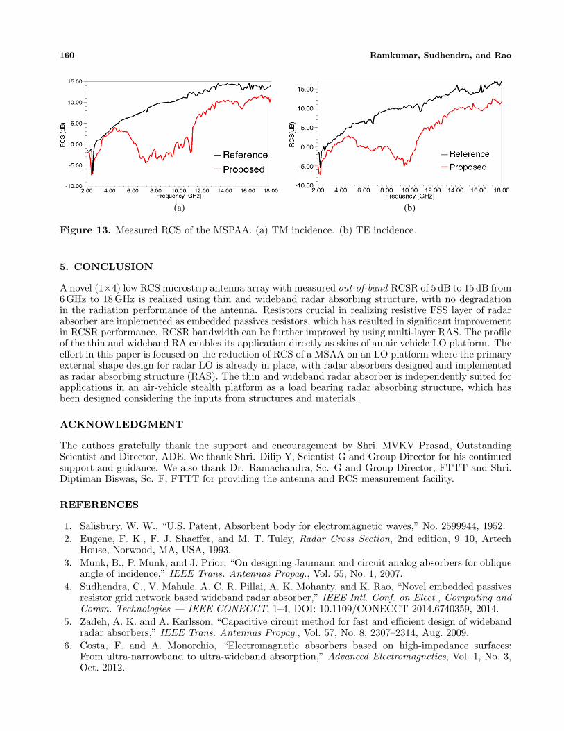
RCS measurements of the reference antenna and the low RCS MSPAA are carried out in microwaveanechoic chamber. The RCS measurement setup is shown in Fig. 12. Comparison plots of RCS of thereference and proposed low RCS antennas for both TE and TM incidences are plotted in Figs. 13(a),(b).
In a ‘pseudo’ monostatic RCS measurement setup, two high directivity horn antennas, one fortransmission and the other for reception are well isolated from each other and located very closely witha bistatic angle of almost zero degrees. An analog phase shifter and attenuator in the coupled ports ofthe two directional couplers connected to the two horn antennas enable ‘vectorial cancellation’ of the RFbackground, at each measurement frequency, in the microwave anechoic chamber. The antenna is placedon a single axis positioner, enabling rotation in azimuth plane. RCS measurement results of the referenceand proposed antenna are plotted in Figs. 13(a) and 13(b), for vertical and horizontal polarizations. Itis observed that the simulated and measured RCS results agree well and indicate accurate simulationand also reliable translation of design to hardware using standard fabrication technology.
160 Ramkumar, Sudhendra, and Rao
(a) (b)
Figure 13. Measured RCS of the MSPAA. (a) TM incidence. (b) TE incidence.
5. CONCLUSION
A novel (1×4) low RCS microstrip antenna array with measured out-of-band RCSR of 5 dB to 15 dB from6GHz to 18 GHz is realized using thin and wideband radar absorbing structure, with no degradationin the radiation performance of the antenna. Resistors crucial in realizing resistive FSS layer of radarabsorber are implemented as embedded passives resistors, which has resulted in significant improvementin RCSR performance. RCSR bandwidth can be further improved by using multi-layer RAS. The profileof the thin and wideband RA enables its application directly as skins of an air vehicle LO platform. Theeffort in this paper is focused on the reduction of RCS of a MSAA on an LO platform where the primaryexternal shape design for radar LO is already in place, with radar absorbers designed and implementedas radar absorbing structure (RAS). The thin and wideband radar absorber is independently suited forapplications in an air-vehicle stealth platform as a load bearing radar absorbing structure, which hasbeen designed considering the inputs from structures and materials.
ACKNOWLEDGMENT
The authors gratefully thank the support and encouragement by Shri. MVKV Prasad, OutstandingScientist and Director, ADE. We thank Shri. Dilip Y, Scientist G and Group Director for his continuedsupport and guidance. We also thank Dr. Ramachandra, Sc. G and Group Director, FTTT and Shri.Diptiman Biswas, Sc. F, FTTT for providing the antenna and RCS measurement facility.
REFERENCES
1. Salisbury, W. W., “U.S. Patent, Absorbent body for electromagnetic waves,” No. 2599944, 1952.2. Eugene, F. K., F. J. Shaeffer, and M. T. Tuley, Radar Cross Section, 2nd edition, 9–10, Artech
House, Norwood, MA, USA, 1993.3. Munk, B., P. Munk, and J. Prior, “On designing Jaumann and circuit analog absorbers for oblique
angle of incidence,” IEEE Trans. Antennas Propag., Vol. 55, No. 1, 2007.4. Sudhendra, C., V. Mahule, A. C. R. Pillai, A. K. Mohanty, and K. Rao, “Novel embedded passives
resistor grid network based wideband radar absorber,” IEEE Intl. Conf. on Elect., Computing andComm. Technologies — IEEE CONECCT, 1–4, DOI: 10.1109/CONECCT 2014.6740359, 2014.
5. Zadeh, A. K. and A. Karlsson, “Capacitive circuit method for fast and efficient design of widebandradar absorbers,” IEEE Trans. Antennas Propag., Vol. 57, No. 8, 2307–2314, Aug. 2009.
6. Costa, F. and A. Monorchio, “Electromagnetic absorbers based on high-impedance surfaces:From ultra-narrowband to ultra-wideband absorption,” Advanced Electromagnetics, Vol. 1, No. 3,Oct. 2012.
Progress In Electromagnetics Research C, Vol. 68, 2016 161
7. Silva, M. W. B., A. L. P. S. Campos, and L. C. Kretly, “Design of thin microwave absorbers usinglossy frequency selective surfaces,” Microw. Opt. Technol. Lett., Vol. 57, No. 4, Apr. 2015.
8. Hansen, R. C., “Relationships between antennas as scatterers and radiators,” Proc. IEEE, Vol. 77,No. 5, 659–662, May 1989.
9. Genovesi, S., F. Costa, and A. Monorchio, “Low-profile array with reduced radar cross section byusing hybrid frequency selective surfaces,” IEEE Trans. Antennas Propag., Vol. 60, No. 5, 2327–2335, May 2012.
10. Zheng, J., S. Fang, Y. Jia, and Y. Liu, “RCS reduction of patch array antenna by complementarysplit-ring resonators structure,” Progress In Electromagnetics Research C, Vol. 51, 95–101, 2014.
11. Joozdani, M. Z., M. K. Amirhosseini, and A. Abdolali, “Wideband radar cross-section of patcharray antenna with miniaturised hexagonal loop frequency selective surface,” Electron. Lett.,Vol. 52, No. 9, 767–768, Apr. 2016.
12. Hao, Y., Y. Liu, K. Li, and S. Gong, “Wide band radar cross section reduction of microstrip patchantenna with split-ring resonators,” Electron. Lett., Vol. 51, No. 20, 1608–1609, Oct. 2015.
13. Liu, Y., Y. Hao, H. Wang, K. Li, and S. Gong, “Low RCS microstrip patch antenna using frequency-selective surface and microstrip resonator,” IEEE Antennas Wireless Propag. Lett., Vol. 14, 1290–1293, Feb. 2015.
14. Jia, Y., Y. Liu, H. Wang, and S. Gong, “Low RCS microstrip antenna using polarization-dependentfrequency selective surface,” Electron. Lett., Vol. 50, No. 14, 978–979, 2014.
15. He, W., R. Jin, and J. Geng, “Low radar cross-section and high performances of microstrip antennausing fractal uniplanar compact electromagnetic band gap ground,” IEEE Microw., AntennasPropag., Vol. 1, No. 5, 986–991, 2007.
16. Miao, Z., C. Huang, X. Ma, M. Pu, X. Ma, Q. Zhao, and X. Luo, “Design of a patch antenna withdual-band radar cross section reduction,” Microw. Opt. Technol. Lett., Vol. 54, No. 11, 2516–2520,Nov. 2012.
17. Zhao, Y., X. Cao, J. Gao, X. Yao, T. Liu, W. Li, and S. Li, “Broadband metamaterial surfacefor antenna RCS reduction and gain enhancement,” IEEE Trans. Antennas Propag., early access,2015.
18. Chen, Q. and Y. Fu, “A planar stealthy antenna Radome using absorptive frequency selectivesurface,” Microw. Opt. Technol. Lett., Vol. 56, No. 8, 1788–1792, 2014.
19. Huang, C., W. Pan, X. Ma, and X. Luo, “A frequency reconfigurable directive antenna withwideband low-RCS property,” IEEE Trans. Antennas Propag., Vol. 64, No. 3, 1173–1178, Jan. 2016.
20. Liu, Y., Y. Hao, K. Li, and S. Gong, “Radar cross section reduction of a microstrip antenna basedon polarization conversion metamaterial,” IEEE Antennas Wireless Propag. Lett., Vol. 15, 80–83,May 2015.
21. Zheng, Y.-J., J. Gao, X.-Y. Cao, S.-J. Li, and W.-Q. Lli, “Wideband RCS reduction andgain enhancement microstrip antenna using chessboard configuration superstrate,” Microw. Opt.Technol. Lett., Vol. 56, No. 8, 1788–1792, 2014.
22. Zheng, J. and S. Fang, “A new method for designing low RCS patch antenna using frequencyselective surface,” Progress In Electromagnetics Research Letters, Vol. 57, No. 7, 1738–1741,Jul. 2015.
23. Huang, C., W. Pan, X. Ma, B. Jiang, and X. Luo, “Wideband radar cross section reduction of astacked patch array antenna using metasurface,” IEEE Antennas Wireless Propag. Lett., Vol. 14,1369–1372, 2015.
24. Rozanov, K. N., “Ultimate thickness to bandwidth ratio of radar absorbers,” IEEE Trans. AntennasPropag., Vol. 48, No. 8, 1230–1234, Aug. 2000.