Embed Size (px)
Citation preview
A Novel Method for the Fabrication of a High-Density Carbon Nanotube Microelectrode Array
Khalifa, Adam; Gao, Zhaoli; Bermak, Amine; Wang, Yi; Hang Chan, Leanne Lai
Published in:Sensing and Bio-Sensing Research
Published: 01/09/2015
Document Version:Final Published version, also known as Publisher’s PDF, Publisher’s Final version or Version of Record
License:CC BY-NC-ND
Publication record in CityU Scholars:Go to record
Published version (DOI):10.1016/j.sbsr.2015.04.001
Publication details:Khalifa, A., Gao, Z., Bermak, A., Wang, Y., & Hang Chan, L. L. (2015). A Novel Method for the Fabrication of aHigh-Density Carbon Nanotube Microelectrode Array. Sensing and Bio-Sensing Research, 5, 1-7.https://doi.org/10.1016/j.sbsr.2015.04.001
Citing this paperPlease note that where the full-text provided on CityU Scholars is the Post-print version (also known as Accepted AuthorManuscript, Peer-reviewed or Author Final version), it may differ from the Final Published version. When citing, ensure thatyou check and use the publisher's definitive version for pagination and other details.
General rightsCopyright for the publications made accessible via the CityU Scholars portal is retained by the author(s) and/or othercopyright owners and it is a condition of accessing these publications that users recognise and abide by the legalrequirements associated with these rights. Users may not further distribute the material or use it for any profit-making activityor commercial gain.Publisher permissionPermission for previously published items are in accordance with publisher's copyright policies sourced from the SHERPARoMEO database. Links to full text versions (either Published or Post-print) are only available if corresponding publishersallow open access.
Take down policyContact [email protected] if you believe that this document breaches copyright and provide us with details. We willremove access to the work immediately and investigate your claim.
Download date: 01/02/2022
Sensing and Bio-Sensing Research 5 (2015) 1–7
Contents lists available at ScienceDirect
Sensing and Bio-Sensing Research
journal homepage: www.elsevier .com/locate /sbsr
A novel method for the fabrication of a high-density carbon nanotubemicroelectrode array
http://dx.doi.org/10.1016/j.sbsr.2015.04.0012214-1804/� 2015 The Authors. Published by Elsevier B.V.This is an open access article under the CC BY-NC-ND license (http://creativecommons.org/licenses/by-nc-nd/4.0/).
⇑ Corresponding author. Tel.: +1 443 825 2009.E-mail addresses: [email protected] (A. Khalifa), [email protected]
(L.L. Hang Chan).
Adam Khalifa a,⇑, Zhaoli Gao b, Amine Bermak a, Yi Wang c, Leanne Lai Hang Chan c
a Department of Electrical and Computer Engineering, Hong Kong University of Science and Technology, Hong Kong, Chinab Department of Mechanical Engineering, Hong Kong University of Science and Technology, Hong Kong, Chinac Department of Electronic Engineering, City University of Hong Kong, Hong Kong, China
a r t i c l e i n f o a b s t r a c t
Keywords:
Microelectrode arrayNeural implantCarbon nanotubesThrough-silicon via interconnectsMicrofabricationWe present a novel method for fabricating a high-density carbon nanotube microelectrode array (MEA)chip. Vertically aligned carbon nanotubes (VACNTs) were synthesized by microwave plasma-enhancedchemical vapor deposition and thermal chemical vapor deposition. The device was characterized usingelectrochemical experiments such as cyclic voltammetry, impedance spectroscopy and potential tran-sient measurements. Through-silicon vias (TSVs) were fabricated and partially filled with polycrystallinesilicon to allow electrical connection from the high-density electrodes to a stimulator microchip. Inresponse to the demand for higher resolution implants, we have developed a unique process to obtaina high-density electrode array by making the microelectrodes smaller in size and designing new waysof routing the electrodes to current sources.
� 2015 The Authors. Published by Elsevier B.V. This is an open access article under the CC BY-NC-NDlicense (http://creativecommons.org/licenses/by-nc-nd/4.0/).
1. Introduction
Over the last few decades, with the help of miniaturized neuralcircuits, a lot of effort have been put into understanding the ner-vous system and developing prostheses. Biocompatibility and highresolution are one of the most important requirements forstate-of-the-art medical implants.
A good example is the epiretinal prosthesis, a device that is ableto electrically stimulate surviving retinal cells of patients sufferingfrom diseases such as retinitis pigmentosa (RP) and age-relatedmacular degeneration (AMD). A large percentage of patients withAMD retain good peripheral vision. In contrast, many patients withadvanced RP retain their central vision. Thus, implantation of aretinal prosthesis would be justified for such patients only if itprovided a substantial improvement in visual acuity; otherwisethey would not benefit from it. Studies show that a retinal prosthe-sis must have about 1000 pixels/electrodes to restore functionssuch as face recognition, reading and unaided mobility [1].Unfortunately, most of the epiretinal prostheses currently underdevelopment comprise arrays of as few as 60 electrodes, each withdiameters of 100 micrometers or more [2–5]. These implants
provide very limited vision, allowing patients to only see spots oflight and high-contrast edges.
The design of high density microelectrode arrays presents sev-eral engineering and biological challenges. For instance, having1000 electrodes confined in an area of 30 mm2 (area of the macula)leads to two major issues: (1) at least 10 conducting lines wouldneed to pass between electrodes, which would produce largecapacitive coupling and be very difficult to fabricate and (2) thecenter-to-center distance between electrodes cannot exceed150 lm, thus the electrode diameter has to be made small enoughin order to avoid cross-talk, and most electrodes with a diameterthat small (usually <100 lm) cannot deliver enough charge toexceed the stimulation threshold of nerve cells without conflictingwith the electrochemical safety requirements.
The first challenging issue, which is the routing of signals fromthe current sources to the stimulating electrodes, has beenaddressed by patterning the conducting lines on different planesand using vias to connect the planes to each other [6,7]. Howeverthis increases the thickness of the device (leading to large stiffness)and greatly complicates the fabrication process flow. Someresearchers have overcome the interconnect limitation by design-ing novel MEA systems and making use of multi-microchip archi-tectures, which consist of multiple chips, each comprising severalelectrodes and a control circuit [8,9]. This approach offers the pos-sibility of connecting several microchips via a bus system, whichenables a decrease in the number of connection lines. However this
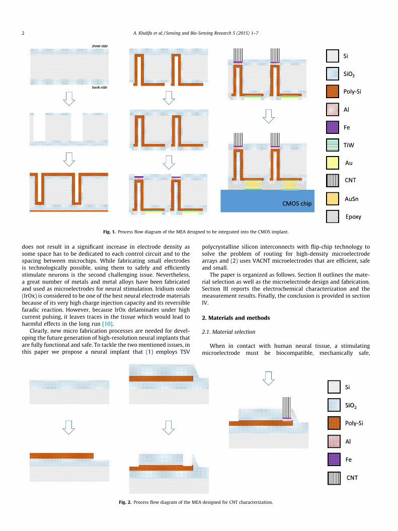
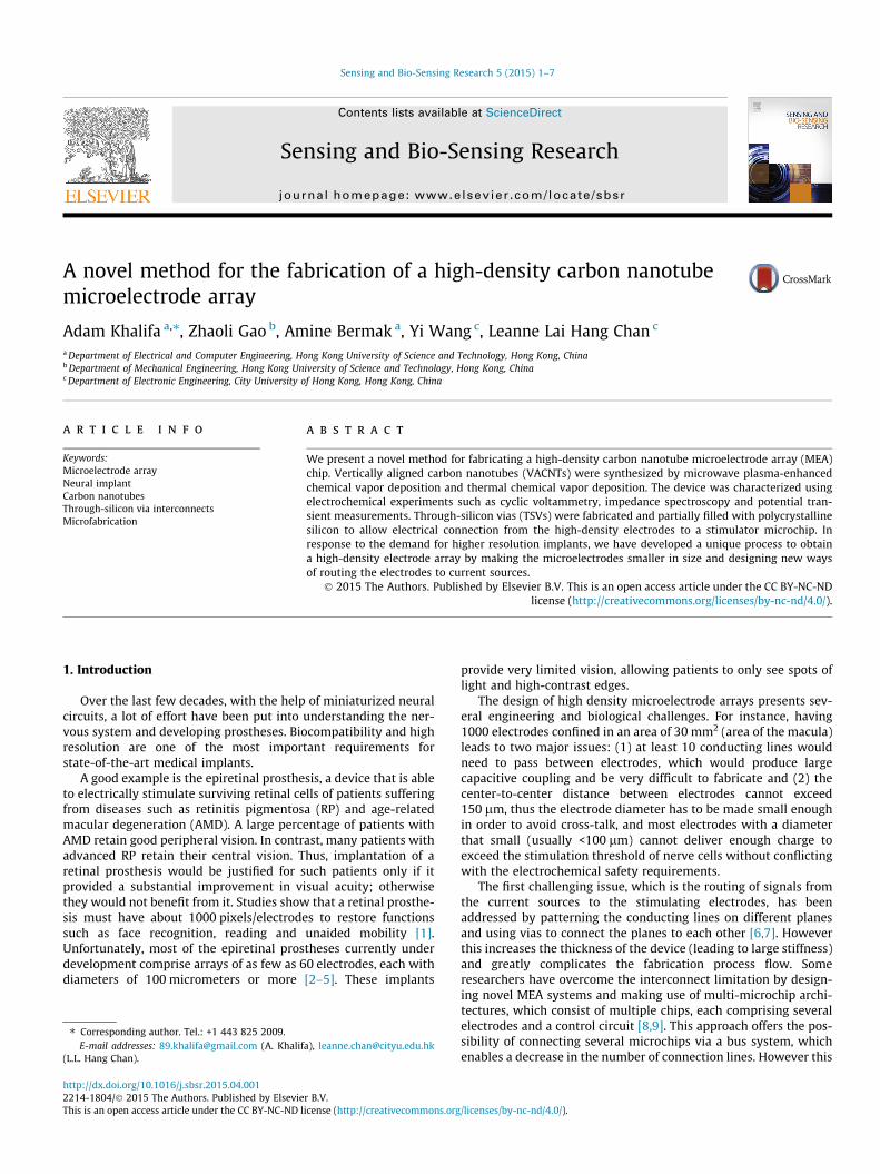
Fig. 1. Process flow diagram of the MEA designed to be integrated into the CMOS implant.
2 A. Khalifa et al. / Sensing and Bio-Sensing Research 5 (2015) 1–7
does not result in a significant increase in electrode density assome space has to be dedicated to each control circuit and to thespacing between microchips. While fabricating small electrodesis technologically possible, using them to safely and efficientlystimulate neurons is the second challenging issue. Nevertheless,a great number of metals and metal alloys have been fabricatedand used as microelectrodes for neural stimulation. Iridium oxide(IrOx) is considered to be one of the best neural electrode materialsbecause of its very high charge injection capacity and its reversiblefaradic reaction. However, because IrOx delaminates under highcurrent pulsing, it leaves traces in the tissue which would lead toharmful effects in the long run [10].
Clearly, new micro fabrication processes are needed for devel-oping the future generation of high-resolution neural implants thatare fully functional and safe. To tackle the two mentioned issues, inthis paper we propose a neural implant that (1) employs TSV
Fig. 2. Process flow diagram of the MEA
polycrystalline silicon interconnects with flip-chip technology tosolve the problem of routing for high-density microelectrodearrays and (2) uses VACNT microelectrodes that are efficient, safeand small.
The paper is organized as follows. Section II outlines the mate-rial selection as well as the microelectrode design and fabrication.Section III reports the electrochemical characterization and themeasurement results. Finally, the conclusion is provided in sectionIV.
2. Materials and methods
2.1. Material selection
When in contact with human neural tissue, a stimulatingmicroelectrode must be biocompatible, mechanically safe,
designed for CNT characterization.
A. Khalifa et al. / Sensing and Bio-Sensing Research 5 (2015) 1–7 3
electrochemically safe and stable. One candidate that can operateunder these demanding conditions when miniaturized is CNTs.They have shown a combination of flexibility and mechanical sta-bility with Young’s modulus in the range of 1–1.8 TPa, makingthem capable of penetrating neural tissue without inducing anydamage to themselves. Experiment evidence shows that CNTs arenot only biocompatible but also chemically inert [11,12] and thatcharge transfer of CNTs in an electrolytic medium is mostlynon-faradaic, thus preventing the formation of reduction andoxidation species [13]. CNTs are highly porous and because of thisfeature the electrolytes should be able to penetrate through thesurface to gain access to the interior surface. However CNTs arealso hydrophobic materials [14]; hence most of their large interiorsurface area is inaccessible in aqueous solution and thus cannotcontribute to charge injection. Thus, it is essential to modify theCNTs’ surfaces to become hydrophilic.
CNTs have mainly been grown on insulating materials such asSiO2 because metal catalysts tend to form alloys with conductingsubstrates at high temperatures. To prevent intermixing of catalystand substrate, a conducting buffer layer can be used. In order tohave a good adhesion to the catalyst and the interconnect, the rightunderlayer material with the right thickness must be carefully cho-sen [15,16]. Most importantly, it is crucial for the diffusion barriernot to react with the catalyst so that the catalyst film can easilyform uniform and discrete nanoparticles. In this study aluminum(Al) and titanium (Ti) have been used (separately) as underlayers.
Metals are not used as our electrical conducting lead materialsince most metals would not survive the high process temperatureof the microwave plasma enhanced chemical vapor depositionmachine (900�C). Those who do have high melting points show avery high chance of forming microscopic cracks due to a muchhigher thermal expansion than that of silicon dioxide(0.5 � 10�6 K�1). For instance, titanium nitride has a thermalexpansion coefficient of 9.35 � 10�6 K�1. Furthermore, unlikeCVD, it is difficult to grow a conformal film in high aspect ratiotrenches by sputter deposition. Sputtering into these featuresresults in poor step coverage and large overhang, which leads tovoid formation. Given the harsh fabrication requirements, heavilydoped polycrystalline silicon (poly-Si) is used as metal intercon-nects. It has a good interface with silicon dioxide and most impor-tantly it keeps the fabrication process at a ‘‘Clean CMOS’’ statewhich allows, for example, the deposition of silicon dioxide ofhigher quality.
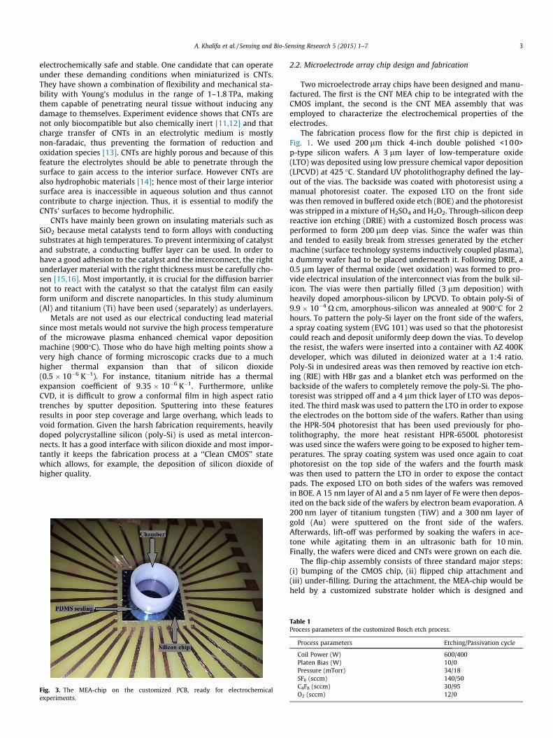
Fig. 3. The MEA-chip on the customized PCB, ready for electrochemicalexperiments.
2.2. Microelectrode array chip design and fabrication
Two microelectrode array chips have been designed and manu-factured. The first is the CNT MEA chip to be integrated with theCMOS implant, the second is the CNT MEA assembly that wasemployed to characterize the electrochemical properties of theelectrodes.
The fabrication process flow for the first chip is depicted inFig. 1. We used 200 lm thick 4-inch double polished <100>p-type silicon wafers. A 3 lm layer of low-temperature oxide(LTO) was deposited using low pressure chemical vapor deposition(LPCVD) at 425 �C. Standard UV photolithography defined the lay-out of the vias. The backside was coated with photoresist using amanual photoresist coater. The exposed LTO on the front sidewas then removed in buffered oxide etch (BOE) and the photoresistwas stripped in a mixture of H2SO4 and H2O2. Through-silicon deepreactive ion etching (DRIE) with a customized Bosch process wasperformed to form 200 lm deep vias. Since the wafer was thinand tended to easily break from stresses generated by the etchermachine (surface technology systems inductively coupled plasma),a dummy wafer had to be placed underneath it. Following DRIE, a0.5 lm layer of thermal oxide (wet oxidation) was formed to pro-vide electrical insulation of the interconnect vias from the bulk sil-icon. The vias were then partially filled (3 lm deposition) withheavily doped amorphous-silicon by LPCVD. To obtain poly-Si of9.9 � 10�4 X cm, amorphous-silicon was annealed at 900�C for 2hours. To pattern the poly-Si layer on the front side of the wafers,a spray coating system (EVG 101) was used so that the photoresistcould reach and deposit uniformly deep down the vias. To developthe resist, the wafers were inserted into a container with AZ 400Kdeveloper, which was diluted in deionized water at a 1:4 ratio.Poly-Si in undesired areas was then removed by reactive ion etch-ing (RIE) with HBr gas and a blanket etch was performed on thebackside of the wafers to completely remove the poly-Si. The pho-toresist was stripped off and a 4 lm thick layer of LTO was depos-ited. The third mask was used to pattern the LTO in order to exposethe electrodes on the bottom side of the wafers. Rather than usingthe HPR-504 photoresist that has been used previously for pho-tolithography, the more heat resistant HPR-6500L photoresistwas used since the wafers were going to be exposed to higher tem-peratures. The spray coating system was used once again to coatphotoresist on the top side of the wafers and the fourth maskwas then used to pattern the LTO in order to expose the contactpads. The exposed LTO on both sides of the wafers was removedin BOE. A 15 nm layer of Al and a 5 nm layer of Fe were then depos-ited on the back side of the wafers by electron beam evaporation. A200 nm layer of titanium tungsten (TiW) and a 300 nm layer ofgold (Au) were sputtered on the front side of the wafers.Afterwards, lift-off was performed by soaking the wafers in ace-tone while agitating them in an ultrasonic bath for 10 min.Finally, the wafers were diced and CNTs were grown on each die.
The flip-chip assembly consists of three standard major steps:(i) bumping of the CMOS chip, (ii) flipped chip attachment and(iii) under-filling. During the attachment, the MEA-chip would beheld by a customized substrate holder which is designed and
Table 1Process parameters of the customized Bosch etch process.
Process parameters Etching/Passivation cycle
Coil Power (W) 600/400Platen Bias (W) 10/0Pressure (mTorr) 34/18SF6 (sccm) 140/50C4F8 (sccm) 30/95O2 (sccm) 12/0
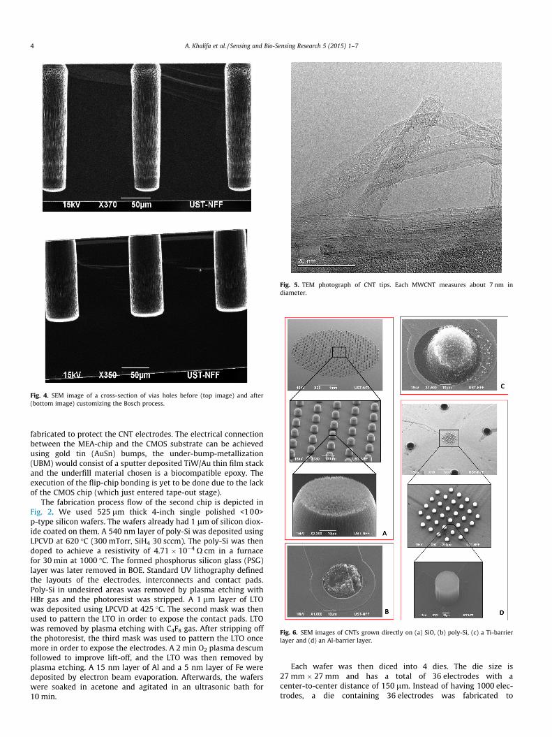
Fig. 4. SEM image of a cross-section of vias holes before (top image) and after(bottom image) customizing the Bosch process.
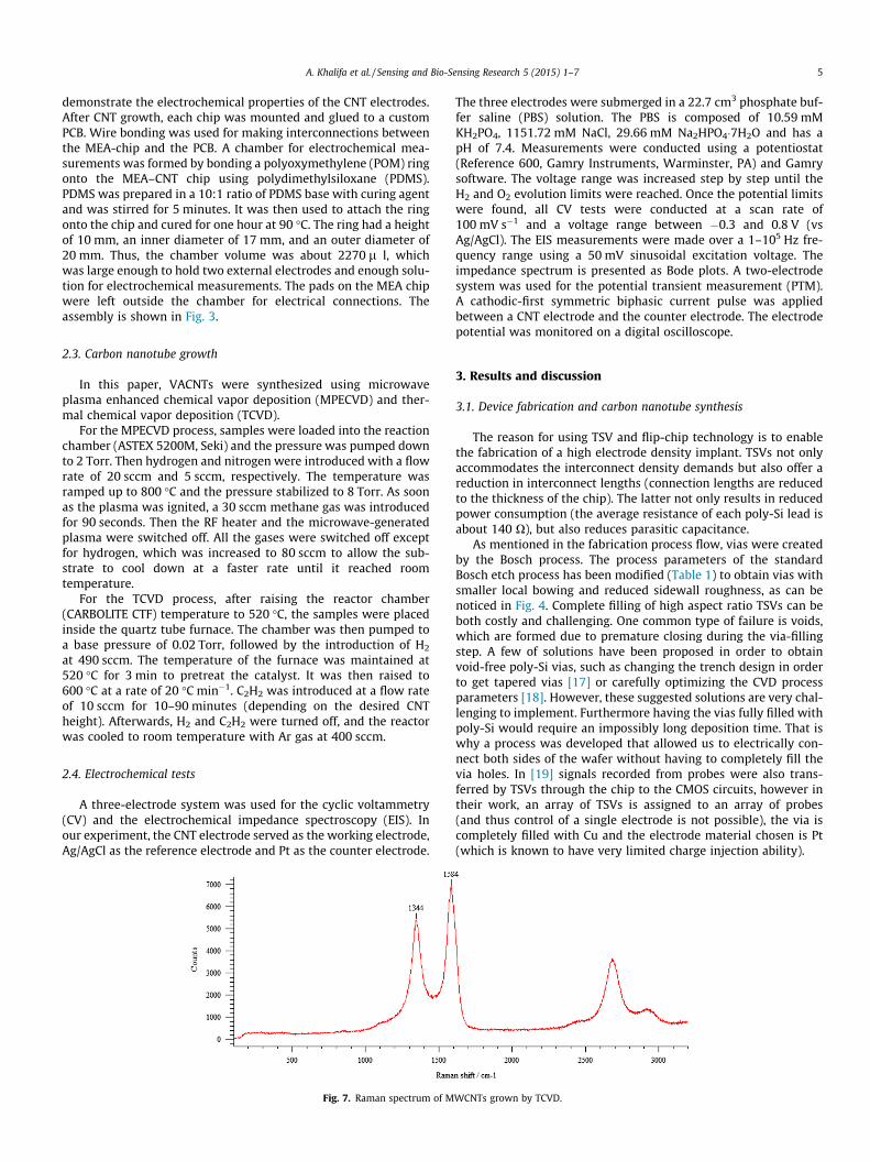
Fig. 5. TEM photograph of CNT tips. Each MWCNT measures about 7 nm indiameter.
Fig. 6. SEM images of CNTs grown directly on (a) SiO, (b) poly-Si, (c) a Ti-barrierlayer and (d) an Al-barrier layer.
4 A. Khalifa et al. / Sensing and Bio-Sensing Research 5 (2015) 1–7
fabricated to protect the CNT electrodes. The electrical connectionbetween the MEA-chip and the CMOS substrate can be achievedusing gold tin (AuSn) bumps, the under-bump-metallization(UBM) would consist of a sputter deposited TiW/Au thin film stackand the underfill material chosen is a biocompatible epoxy. Theexecution of the flip-chip bonding is yet to be done due to the lackof the CMOS chip (which just entered tape-out stage).
The fabrication process flow of the second chip is depicted inFig. 2. We used 525 lm thick 4-inch single polished <100>p-type silicon wafers. The wafers already had 1 lm of silicon diox-ide coated on them. A 540 nm layer of poly-Si was deposited usingLPCVD at 620 �C (300 mTorr, SiH4 30 sccm). The poly-Si was thendoped to achieve a resistivity of 4.71 � 10�4 X cm in a furnacefor 30 min at 1000 �C. The formed phosphorus silicon glass (PSG)layer was later removed in BOE. Standard UV lithography definedthe layouts of the electrodes, interconnects and contact pads.Poly-Si in undesired areas was removed by plasma etching withHBr gas and the photoresist was stripped. A 1 lm layer of LTOwas deposited using LPCVD at 425 �C. The second mask was thenused to pattern the LTO in order to expose the contact pads. LTOwas removed by plasma etching with C4F8 gas. After stripping offthe photoresist, the third mask was used to pattern the LTO oncemore in order to expose the electrodes. A 2 min O2 plasma descumfollowed to improve lift-off, and the LTO was then removed byplasma etching. A 15 nm layer of Al and a 5 nm layer of Fe weredeposited by electron beam evaporation. Afterwards, the waferswere soaked in acetone and agitated in an ultrasonic bath for10 min.
Each wafer was then diced into 4 dies. The die size is27 mm � 27 mm and has a total of 36 electrodes with acenter-to-center distance of 150 lm. Instead of having 1000 elec-trodes, a die containing 36 electrodes was fabricated to
A. Khalifa et al. / Sensing and Bio-Sensing Research 5 (2015) 1–7 5
demonstrate the electrochemical properties of the CNT electrodes.After CNT growth, each chip was mounted and glued to a customPCB. Wire bonding was used for making interconnections betweenthe MEA-chip and the PCB. A chamber for electrochemical mea-surements was formed by bonding a polyoxymethylene (POM) ringonto the MEA–CNT chip using polydimethylsiloxane (PDMS).PDMS was prepared in a 10:1 ratio of PDMS base with curing agentand was stirred for 5 minutes. It was then used to attach the ringonto the chip and cured for one hour at 90 �C. The ring had a heightof 10 mm, an inner diameter of 17 mm, and an outer diameter of20 mm. Thus, the chamber volume was about 2270 l l, whichwas large enough to hold two external electrodes and enough solu-tion for electrochemical measurements. The pads on the MEA chipwere left outside the chamber for electrical connections. Theassembly is shown in Fig. 3.
2.3. Carbon nanotube growth
In this paper, VACNTs were synthesized using microwaveplasma enhanced chemical vapor deposition (MPECVD) and ther-mal chemical vapor deposition (TCVD).
For the MPECVD process, samples were loaded into the reactionchamber (ASTEX 5200M, Seki) and the pressure was pumped downto 2 Torr. Then hydrogen and nitrogen were introduced with a flowrate of 20 sccm and 5 sccm, respectively. The temperature wasramped up to 800 �C and the pressure stabilized to 8 Torr. As soonas the plasma was ignited, a 30 sccm methane gas was introducedfor 90 seconds. Then the RF heater and the microwave-generatedplasma were switched off. All the gases were switched off exceptfor hydrogen, which was increased to 80 sccm to allow the sub-strate to cool down at a faster rate until it reached roomtemperature.
For the TCVD process, after raising the reactor chamber(CARBOLITE CTF) temperature to 520 �C, the samples were placedinside the quartz tube furnace. The chamber was then pumped toa base pressure of 0.02 Torr, followed by the introduction of H2
at 490 sccm. The temperature of the furnace was maintained at520 �C for 3 min to pretreat the catalyst. It was then raised to600 �C at a rate of 20 �C min�1. C2H2 was introduced at a flow rateof 10 sccm for 10–90 minutes (depending on the desired CNTheight). Afterwards, H2 and C2H2 were turned off, and the reactorwas cooled to room temperature with Ar gas at 400 sccm.
2.4. Electrochemical tests
A three-electrode system was used for the cyclic voltammetry(CV) and the electrochemical impedance spectroscopy (EIS). Inour experiment, the CNT electrode served as the working electrode,Ag/AgCl as the reference electrode and Pt as the counter electrode.
Fig. 7. Raman spectrum of M
The three electrodes were submerged in a 22.7 cm3 phosphate buf-fer saline (PBS) solution. The PBS is composed of 10.59 mMKH2PO4, 1151.72 mM NaCl, 29.66 mM Na2HPO4�7H2O and has apH of 7.4. Measurements were conducted using a potentiostat(Reference 600, Gamry Instruments, Warminster, PA) and Gamrysoftware. The voltage range was increased step by step until theH2 and O2 evolution limits were reached. Once the potential limitswere found, all CV tests were conducted at a scan rate of100 mV s�1 and a voltage range between �0.3 and 0.8 V (vsAg/AgCl). The EIS measurements were made over a 1–105 Hz fre-quency range using a 50 mV sinusoidal excitation voltage. Theimpedance spectrum is presented as Bode plots. A two-electrodesystem was used for the potential transient measurement (PTM).A cathodic-first symmetric biphasic current pulse was appliedbetween a CNT electrode and the counter electrode. The electrodepotential was monitored on a digital oscilloscope.
3. Results and discussion
3.1. Device fabrication and carbon nanotube synthesis
The reason for using TSV and flip-chip technology is to enablethe fabrication of a high electrode density implant. TSVs not onlyaccommodates the interconnect density demands but also offer areduction in interconnect lengths (connection lengths are reducedto the thickness of the chip). The latter not only results in reducedpower consumption (the average resistance of each poly-Si lead isabout 140 X), but also reduces parasitic capacitance.
As mentioned in the fabrication process flow, vias were createdby the Bosch process. The process parameters of the standardBosch etch process has been modified (Table 1) to obtain vias withsmaller local bowing and reduced sidewall roughness, as can benoticed in Fig. 4. Complete filling of high aspect ratio TSVs can beboth costly and challenging. One common type of failure is voids,which are formed due to premature closing during the via-fillingstep. A few of solutions have been proposed in order to obtainvoid-free poly-Si vias, such as changing the trench design in orderto get tapered vias [17] or carefully optimizing the CVD processparameters [18]. However, these suggested solutions are very chal-lenging to implement. Furthermore having the vias fully filled withpoly-Si would require an impossibly long deposition time. That iswhy a process was developed that allowed us to electrically con-nect both sides of the wafer without having to completely fill thevia holes. In [19] signals recorded from probes were also trans-ferred by TSVs through the chip to the CMOS circuits, however intheir work, an array of TSVs is assigned to an array of probes(and thus control of a single electrode is not possible), the via iscompletely filled with Cu and the electrode material chosen is Pt(which is known to have very limited charge injection ability).
WCNTs grown by TCVD.
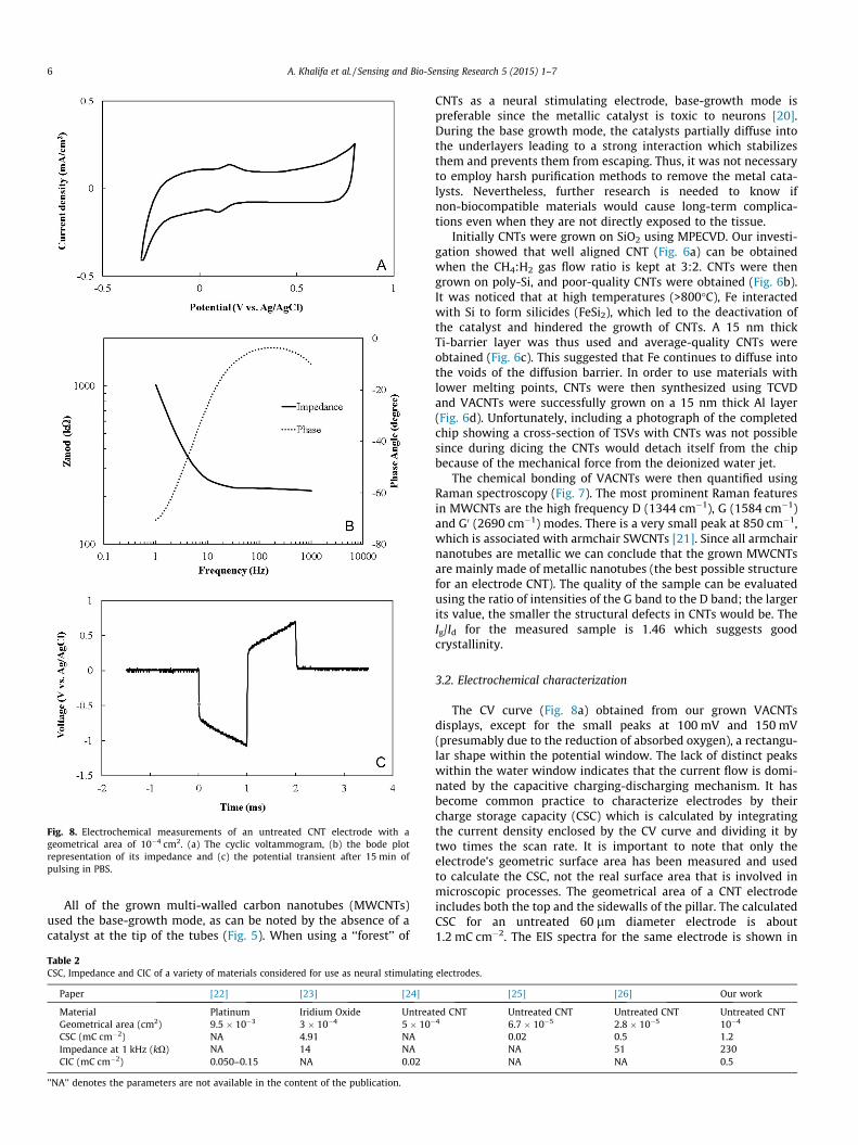
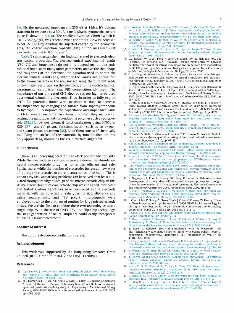
Fig. 8. Electrochemical measurements of an untreated CNT electrode with ageometrical area of 10�4 cm2. (a) The cyclic voltammogram, (b) the bode plotrepresentation of its impedance and (c) the potential transient after 15 min ofpulsing in PBS.
6 A. Khalifa et al. / Sensing and Bio-Sensing Research 5 (2015) 1–7
All of the grown multi-walled carbon nanotubes (MWCNTs)used the base-growth mode, as can be noted by the absence of acatalyst at the tip of the tubes (Fig. 5). When using a ‘‘forest’’ of
Table 2CSC, Impedance and CIC of a variety of materials considered for use as neural stimulating
Paper [22] [23] [24]
Material Platinum Iridium Oxide UntreaGeometrical area (cm2) 9.5 � 10�3 3 � 10�4 5 � 10�
CSC (mC cm�2) NA 4.91 NAImpedance at 1 kHz (kX) NA 14 NACIC (mC cm�2) 0.050–0.15 NA 0.02
’’NA’’ denotes the parameters are not available in the content of the publication.
CNTs as a neural stimulating electrode, base-growth mode ispreferable since the metallic catalyst is toxic to neurons [20].During the base growth mode, the catalysts partially diffuse intothe underlayers leading to a strong interaction which stabilizesthem and prevents them from escaping. Thus, it was not necessaryto employ harsh purification methods to remove the metal cata-lysts. Nevertheless, further research is needed to know ifnon-biocompatible materials would cause long-term complica-tions even when they are not directly exposed to the tissue.
Initially CNTs were grown on SiO2 using MPECVD. Our investi-gation showed that well aligned CNT (Fig. 6a) can be obtainedwhen the CH4:H2 gas flow ratio is kept at 3:2. CNTs were thengrown on poly-Si, and poor-quality CNTs were obtained (Fig. 6b).It was noticed that at high temperatures (>800�C), Fe interactedwith Si to form silicides (FeSi2), which led to the deactivation ofthe catalyst and hindered the growth of CNTs. A 15 nm thickTi-barrier layer was thus used and average-quality CNTs wereobtained (Fig. 6c). This suggested that Fe continues to diffuse intothe voids of the diffusion barrier. In order to use materials withlower melting points, CNTs were then synthesized using TCVDand VACNTs were successfully grown on a 15 nm thick Al layer(Fig. 6d). Unfortunately, including a photograph of the completedchip showing a cross-section of TSVs with CNTs was not possiblesince during dicing the CNTs would detach itself from the chipbecause of the mechanical force from the deionized water jet.
The chemical bonding of VACNTs were then quantified usingRaman spectroscopy (Fig. 7). The most prominent Raman featuresin MWCNTs are the high frequency D (1344 cm�1), G (1584 cm�1)and G0 (2690 cm�1) modes. There is a very small peak at 850 cm�1,which is associated with armchair SWCNTs [21]. Since all armchairnanotubes are metallic we can conclude that the grown MWCNTsare mainly made of metallic nanotubes (the best possible structurefor an electrode CNT). The quality of the sample can be evaluatedusing the ratio of intensities of the G band to the D band; the largerits value, the smaller the structural defects in CNTs would be. TheIg/Id for the measured sample is 1.46 which suggests goodcrystallinity.
3.2. Electrochemical characterization
The CV curve (Fig. 8a) obtained from our grown VACNTsdisplays, except for the small peaks at 100 mV and 150 mV(presumably due to the reduction of absorbed oxygen), a rectangu-lar shape within the potential window. The lack of distinct peakswithin the water window indicates that the current flow is domi-nated by the capacitive charging-discharging mechanism. It hasbecome common practice to characterize electrodes by theircharge storage capacity (CSC) which is calculated by integratingthe current density enclosed by the CV curve and dividing it bytwo times the scan rate. It is important to note that only theelectrode’s geometric surface area has been measured and usedto calculate the CSC, not the real surface area that is involved inmicroscopic processes. The geometrical area of a CNT electrodeincludes both the top and the sidewalls of the pillar. The calculatedCSC for an untreated 60 lm diameter electrode is about1.2 mC cm�2. The EIS spectra for the same electrode is shown in
electrodes.
[25] [26] Our work
ted CNT Untreated CNT Untreated CNT Untreated CNT4 6.7 � 10�5 2.8 � 10�5 10�4
0.02 0.5 1.2NA 51 230NA NA 0.5
A. Khalifa et al. / Sensing and Bio-Sensing Research 5 (2015) 1–7 7
Fig. 8b, the measured impedance is 230 kX at 1 kHz. It’s voltagetransient in response to a 50 lA, 1 ms biphasic symmetric currentpulse is shown in Fig. 8c. The smallest hydrolysis limit (which is�0.3 V vs Ag/AgCl) was reached when the amplitude was increasedto 50 lA. Thus by dividing the injected charge by the geometricarea, the charge injection capacity (CIC) of the measured CNTelectrode is equal to 0.5 mC cm�2.
Table 2 summarizes the main findings related to electrode elec-trochemical properties. The electrochemical experimental results(CSC, CIC and impedance) do not only depend on the electrodematerial but also on many other parameters such as the size, shapeand roughness of the electrode, the equation used to obtain theelectrochemical results (e.g. whether the values are normalizedto the geometric area or the real surface area), the different kindsof treatments performed on the electrode, and the electrochemicalexperimental setup itself (e.g. PBS composition, pH used). Theimpedance of our untreated CNT electrode is too high to be usedas a neural stimulating electrode. Thus, in order to fully exploitCNTs’ full potential, future work needs to be done to decreasethe impedance by changing the surface from superhydrophobicto hydrophilic. To improve the capacitance and impedance valueof CNTs, several methods have been proposed; they include (a)coating the nanotubes with a conducting polymer such as polypyr-role [25,26]; (b) wet chemical functionalization using HNO3 orKOH [27]; and (c) plasma functionalization such as an oxygenand steam plasma treatment [28]. All of them consist of chemicallymodifying the surface of the nanotube by functionalization, butonly approach (a) maintains the CNTs’ vertical alignment.
4. Conclusion
There is an increasing need for high electrode density implants.While the electrode size continues to scale down, the stimulatingneural microelectrode array has to remain efficient and safe.Furthermore, while the number of electrodes increases, new waysof routing the electrodes to current sources has to be found. This isnot an easy task and arising problems can be solved or at least alle-viated through intelligent design of the microelectrode chip. In thisstudy, a new class of microelectrode chip was designed, fabricatedand tested. Carbon Nanotubes have been used as the electrodematerial, with the objective of satisfying the size, efficiency andsafety requirements; and TSV poly-Si interconnects wereemployed to solve the problem of routing for large microelectrodearrays. We are the first to combine these two technologies into asingle chip. With the use of CNTs, TSV and Flip-Chip technology,the next generation of neural implants could easily incorporateat least 1000 microelectrodes.
Conflict of interest
The authors declare no conflict of interest.
Acknowledgment
This work was supported by the Hong Kong Research GrantCouncil (RGC), Grant Ref 610412 and CityU 11200814.
References
[1] G.J. ChaderÃ, J. Weiland, M.S. Humayun, Artificial vision: needs, functioning,and testing of a retinal electronic prosthesis, Neurotherapy: Prog. Restor.Neurosci. Neurol. 175 (2009) 317.
[2] M.S. Humayun, J.D. Dorn, A.K. Ahuja, A. Caspi, E. Filley, G. Dagnelie, J. Salzmann,A. Santos, J. Duncan, L. DaCruz, Preliminary 6 month results from the Argus IIepiretinal prosthesis feasibility study, in: Engineering in Medicine and BiologySociety, 2009. EMBC 2009. Annual International Conference of the IEEE, 2009,pp. 4566–4568.
[3] G. Roessler, T. Laube, C. Brockmann, T. Kirschkamp, B. Mazinani, M. Goertz, C.Koch, I. Krisch, B. Sellhaus, H.K. Trieu, Implantation and explantation of awireless epiretinal retina implant device: observations during the EPIRET3prospective clinical trial, Invest. Ophthalmol. Vis. Sci. 50 (2009) 3003–3008.
[4] M. Feucht, T. Laube, N. Bornfeld, P. Walter, M. Velikay-Parel, R. Hornig, G.Richard, Development of an epiretinal prosthesis for stimulation of the humanretina, Ophthalmologe 102 (Jul 2005) 688–691.
[5] O. Niina, T. Hirotaka, K. Yoshiuki, K. Toshiya, K. Risato, T. Tetsu, H. Jari,Comparison of electrode materials for the use of retinal prosthesis, Biomed.Mater. Eng. 21 (2011) 83–97.
[6] D.C. Rodger, W. Li, A.J. Fong, H. Ameri, E. Meng, J.W. Burdick, R.R. Roy, V.R.Edgerton, J.D. Weiland, M.S. Humayun, Flexible microfabricated parylenemultielectrode arrays for retinal stimulation and spinal cord field modulation,in: IEEE Engineering in Medicine and Biology Society Special Topic Conferenceon Microtechnologies in Medicine and Biology, Okinawa, 2006.
[7] G. Suaning, M. Schuettler, J. Ordonez, N. Lovell, Fabrication of multi-layer,high-density micro-electrode arrays for neural stimulation and bio-signalrecording, in: Neural Engineering, 2007. CNE’07. 3rd International IEEE/EMBSConference on, 2007, pp. 5–8.
[8] U. Frey, C. Sanchez-Bustamante, T. Ugniwenko, F. Heer, J. Sedivy, S. Hafizovic, B.Roscic, M. Fussenegger, A. Blau, U. Egert, Cell recordings with a CMOS high-density microelectrode array, in: Engineering in Medicine and Biology Society,2007. EMBS 2007. 29th Annual International Conference of the IEEE, 2007, pp.167–170.
[9] J. Ohta, T. Tokuda, K. Kagawa, A. Uehara, Y. Terasawa, K. Shodo, T. Fujikado, Y.Tano, Toward 1000-ch electrode array based on distributed microchiparchitecture for retinal prosthesis, in Circuits and Systems, 2006. ISCAS 2006.Proceedings. 2006 IEEE International Symposium on, 2006, pp. 5 pp.-4122.
[10] S.F. Cogan, A.A. Guzelian, W.F. Agnew, T. Yuen, D.B. McCreery, Over-pulsingdegrades activated iridium oxide films used for intracortical neuralstimulation, J. Neurosci. Methods 137 (2004) 141.
[11] D.A. Nayagam, R.A. Williams, J. Chen, K.A. Magee, J. Irwin, J. Tan, P. Innis, R.T.Leung, S. Finch, C.E. Williams, Biocompatibility of immobilized aligned carbonnanotubes, Small 7 (2011) 1035–1042.
[12] G. Ciofani, V. Raffa, O. Vittorio, A. Cuschieri, T. Pizzorusso, M. Costa, G. Bardi, Invitro and in vivo biocompatibility testing of functionalized carbon nanotubes,in: Carbon Nanotubes, 2010, pp. 67–83.
[13] R.H. Baughman, Electrochemical studies of single-wall carbon nanotubes inaqueous solutions, J. Electroanal. Chem. 488 (2000) 92–98.
[14] W. Yang, P. Thordarson, J.J. Gooding, S.P. Ringer, F. Braet, Carbon nanotubes forbiological and biomedical applications, Nanotechnology 18 (2007) 412001.
[15] X. Sun, K. Li, R. Wu, P. Wilhite, T. Saito, J. Gao, C.Y. Yang, The effect of catalystsand underlayer metals on the properties of PECVD-grown carbonnanostructures, Nanotechnology 21 (2010) 045201.
[16] G.D. Nessim, D. Acquaviva, M. Seita, K.P. O’Brien, C.V. Thompson, The criticalrole of the underlayer material and thickness in growing vertically alignedcarbon nanotubes and nanofibers on metallic substrates by chemical vapordeposition, Adv. Funct. Mater. 20 (2010) 1306–1312.
[17] R. Nagarajan, L. Ebin, L. Dayong, S.C. Seng, K. Prasad, N. Balasubramanian,Development of a novel deep silicon tapered via etch process for through-silicon interconnection in 3-D integrated systems, in: Electronic Componentsand Technology Conference, 2006. Proceedings. 56th, 2006, pp. 5 pp.
[18] P. Dixit, T. Vehmas, S. Vähänen, P. Monnoyer, K. Henttinen, Fabrication andelectrical characterization of high aspect ratio poly-silicon filled through-silicon vias, J. Micromech. Microeng. 22 (2012) 055021.
[19] L. Chou, S. Lee, P. Huang, C. Chang, S. Wu, J. Chiou, C. Chuang, W. Hwang, C. Wu,K. Chen, Integrated microprobe array and CMOS MEMS by TSV technology forbio-signal recording application, in: Electronic Components and TechnologyConference (ECTC), 2014 IEEE 64th, 2014, pp. 512–517.
[20] J. Sohn, Y.H. Yoon, Iron-induced cytotoxicity in cultured rat retinal neurons,Korean J. Ophthalmol. 12 (1998) 77–84.
[21] A. Rao, E. Richter, S. Bandow, B. Chase, P. Eklund, K. Williams, S. Fang, K.Subbaswamy, M. Menon, A. Thess, Diameter-selective Raman scattering fromvibrational modes in carbon nanotubes, Science 275 (1997) 187–191.
[22] T. Rose, L. Robblee, Electrical stimulation with Pt electrodes. VIII.Electrochemically safe charge injection limits with 0.2 ms pulses (neuronalapplication), in: Biomedical Engineering, IEEE Transactions on, vol. 37, pp.1118–1120, 1990.
[23] S. Eick, J. Wallys, B. Hofmann, A. Van Ooyen, U. Schnakenberg, S. Ingebrandt, A.Offenhäusser, Iridium oxide microelectrode arrays for in vitro stimulation ofindividual rat neurons from dissociated cultures, Front. Neuroeng. 2 (2009) 16.
[24] K. Wang, H.A. Fishman, H. Dai, J.S. Harris, Neural stimulation with a carbonnanotube microelectrode array, Nano Lett. 6 (2006) 2043–2048.
[25] T. Nguyen-Vu, H. Chen, A.M. Cassell, R. Andrews, M. Meyyappan, J. Li, Verticallyaligned carbon nanofiber arrays: an advance toward electrical-neuralinterfaces, Small 2 (2006) 89–94.
[26] Y. Lu, T. Li, X. Zhao, M. Li, Y. Cao, H. Yang, Y.Y. Duan, Electrodepositedpolypyrrole/carbon nanotubes composite films electrodes for neuralinterfaces, Biomaterials 31 (2010) 5169–5181.
[27] C. Jiang, L. Li, H. Hao, Carbon nanotube yarns for deep brain stimulationelectrode, IEEE Transact. Neural Syst. Rehabil. Eng. 19 (2011) 612–616.
[28] C. Chen, H. Su, S. Chuang, S. Yen, Y. Chen, Y. Lee, H. Chen, T. Yew, Y. Chang, S.Yeh, Hydrophilic modification of neural microelectrode arrays based on multi-walled carbon nanotubes, Nanotechnology 21 (2010) 485501.