Embed Size (px)
Citation preview

145
Original scientific paper
MIDEM Society
A Novel Space Vector Modulation Based Control Strategy for Z-Source InverterV. Erginer, Ö. Girgin
Department of Electrical Engineering, Yildiz Technical University, Davutpasa-Esenler Istanbul, Turkey
Abstract: In this study, a novel control strategy based on Distributed Space Vector Modulation is proposed to improve dynamic performance of a Z Source Inverter (ZSI) while utilizing only capacitor voltage feedback. Distributed space vector modulation allows ZSI output voltage to be controlled by Z source capacitor voltage with a simple equation. Therefore, only one voltage feedback is enough to control inverter output voltage. Furthermore, zero state is not utilized in the proposed control strategy, so an additional control loop for the modulation index is no longer necessary. Flexible modulation index allows work with flexible dc line voltage and limits the voltage stresses in the inverter switches so ZSI has low cost switches and high efficiency. Moreover, the proposed control method was investigated for both resistive and inductive loads due to ZSI load power factor-dependent characteristics. The effectiveness of the suggested control method is verified by Matlab/Simulink simulations, considering the sudden changes in both the dc source and load level.
Keywords: dc-ac power converters; inverters; power conditioning; impedance source inverters ; power system dynamics; linear feedback control systems.
Kontrolna strategija inverterja na osnovi modulacije prostorskega vektorjaIzvleček: Predstavljena je nova kontrolna strategija na osnovi distribuirane modulacije prostorskega vektorja za izboljšanje dinamičnih lastnosti inverterja z Z virom (ZSI) le z uporabo kapacitivne napetostne povratne zanke. Distribuirana modulacija prostorskega vektorja omogoča nadzor izhodbe napetosti ZSI z napetostjo vhodnega kondenzatorja z eno preprosto enačbo. Za nadzor napetosti je tako potrebna le ena povratna zanka. V strategiji ni uporabljeno ničelno stanje. Kontrolna zanka za modulacijo prav tako ni več potrebna. Fleksibilen modulacijski indeks omogoča delo s fleksibilno dc napetost in omejuje napetostni stres v stikalih inverter, kar omogoča uporabo cenenih stikal z visokim izkoristkom. Predlagana kontrola je bila uporabljena na rezistivnih in induktivnih bremenih. Učinkovitost metode je bila preverjena v Matlab/Simulink okolju.
Ključne besede: dc-ac močnostni pretvornik; inverter; dinamika moči; linearna povratna zanka
* Corresponding Author’s e-mail: [email protected]
Journal of Microelectronics, Electronic Components and MaterialsVol. 48, No. 3(2018), 145 – 153
1 Introduction
Power conditioning units (PCU) are widely used in dif-ferent areas like industry, energy plants, transportation, etc. Z Source Inverter (ZSI) is an emerging and prom-ising topology for these units, having significant ben-efits such as buck-boost capability, low cost, reduced volume, and higher efficiency when compared to Volt-age Source and Current Source Inverters [1]. Due to its advantages, ZSI has been widely investigated from various aspects; i.e., modulation methods, closed loop control methods, design, and novel topologies [2, 3].
Although ZSI has some significant superiorities, it has the drawback of poor dynamic performance. ZSI out-
put voltage amplitude depends on both modulation index (M) and dc line voltage, so it is strictly connected with a shoot through duty ratio (D). ZSI has a buck-boost characteristic; similar to other buck-boost con-verters, the transfer function between shoot through duty ratio and ZSI output has a right half plane zero [4]. RHP zero causes an instability in the system. During step changes in shoot through the duty cycle, an initial collapse dip occurs in the capacitor voltage, followed by a damped oscillation. This causes a disturbance in the output voltage of the inverter [5],[6]. Therefore, proper controller design is needed for high dynamic performance. There are many researches dealing with this problem, and their suggestions can be classified
146
V. Erginer et al; Informacije Midem, Vol. 48, No. 3(2018), 145 – 153
under four groups: capacitor voltage control, direct DC line voltage control, indirect DC line voltage control, and unified control.
Using [7, 8] only capacitor voltage (Vc) has been sug-gested for controlling. In this method, Vc is kept con-stant; however, output voltage stability and voltage stress across switches have not been considered. In [9, 10] one model, predictive control has been proposed to keep Vc constant; however, it has four current sen-sors and a voltage sensor for feedbacks. Therefore, it is too complicated and too expensive. In direct dc line voltage control [6], an external sensing circuit has been given to measure dc line voltage (Vi) directly and sta-bilize it due to the pulsating nature of dc line voltage. However, the complex design of the external sens-ing circuit makes the control system expensive. In [6], [11-13], indirect dc line voltage control methods have been proposed to eliminate Vi measurement problems because of their pulsating nature. Nevertheless, they utilize zero state (Z) as a margin between D and M, because they use the constant modulation index as a result of constant Vi. Thus, they work with a low mod-ulation index and a high dc line voltage. As a result, their voltage stress across bridge switches and switch-ing losses are much higher than they could be. In [14] a unified control method is proposed, with an output voltage control loop getting feedback directly from ZSI output. Shoot through duty ratio and modulation in-dex are controlled simultaneously. The main drawback of this method occurs in grid-tied applications, because output voltage feedback is fixed to network voltage.
Choosing the correct modulation technique is also an important factor for ZSI control design. There are different modulation techniques for ZSI in literature: Simple Boost Control, Maximum Boost Control, Maxi-mum Constant Boost Control, Traditional Space Vector Modulation, and Modified Space Vector Modulation. A detailed comparison of these methods has been given in [15]. It is very important to choose the right modula-tion technique to achieve the lowest voltage stress on switches, highest efficiency, and the lowest THD.
In the majority of power conditioning units, the main goal of the control loops is to achieve a stable output at the desired level. When we consider ZSI in a PCU, the control loop should be focused on getting a stable output voltage. Nevertheless, most previous research-es endeavored to be keep the capacitor voltage (Vc) or dc line voltage (Vi) constant. Moreover, in order to limit voltage stress across inverter bridge and switch-ing losses, ZSI should operate with the lowest possible dc line voltage. None of the aforementioned methods have been taken into account, both in order to simul-taneously obtain a stable output during transients and
to limit switching losses. An indirect output voltage governed by controlling impedance network capacitor voltage is preferred to overcome the drawbacks listed above and to get a simple configuration [16].
ZSI behavior is affected by load power factor and has been investigated in some researches [17-18]. For this reason, the effectiveness of the controller used in ZSI for different power factor levels needs to be validated. In this paper, a PI control strategy has been given con-sidering different power factor levels. Transfer function between shoot through duty ratio and inverter output voltage is needed to design a PI compensator. Thus, a dynamic model of ZSI is obtained by state space aver-aging and small signal analysis. There are some studies about dynamic modelling of ZSI in the literature, such as [8], [13], [19-21]. However, the modulation index is not considered as a control variable. Moreover, they do not consider input voltage as a perturbation source; in this case, the input voltage drop scenario would not be reflected in the model. The ZSI dynamic model, which is given in this research, considers all of these issues and is utilized to control output transfer function. The designed PI controller considering this dynamic model is tested with simulations.
a)
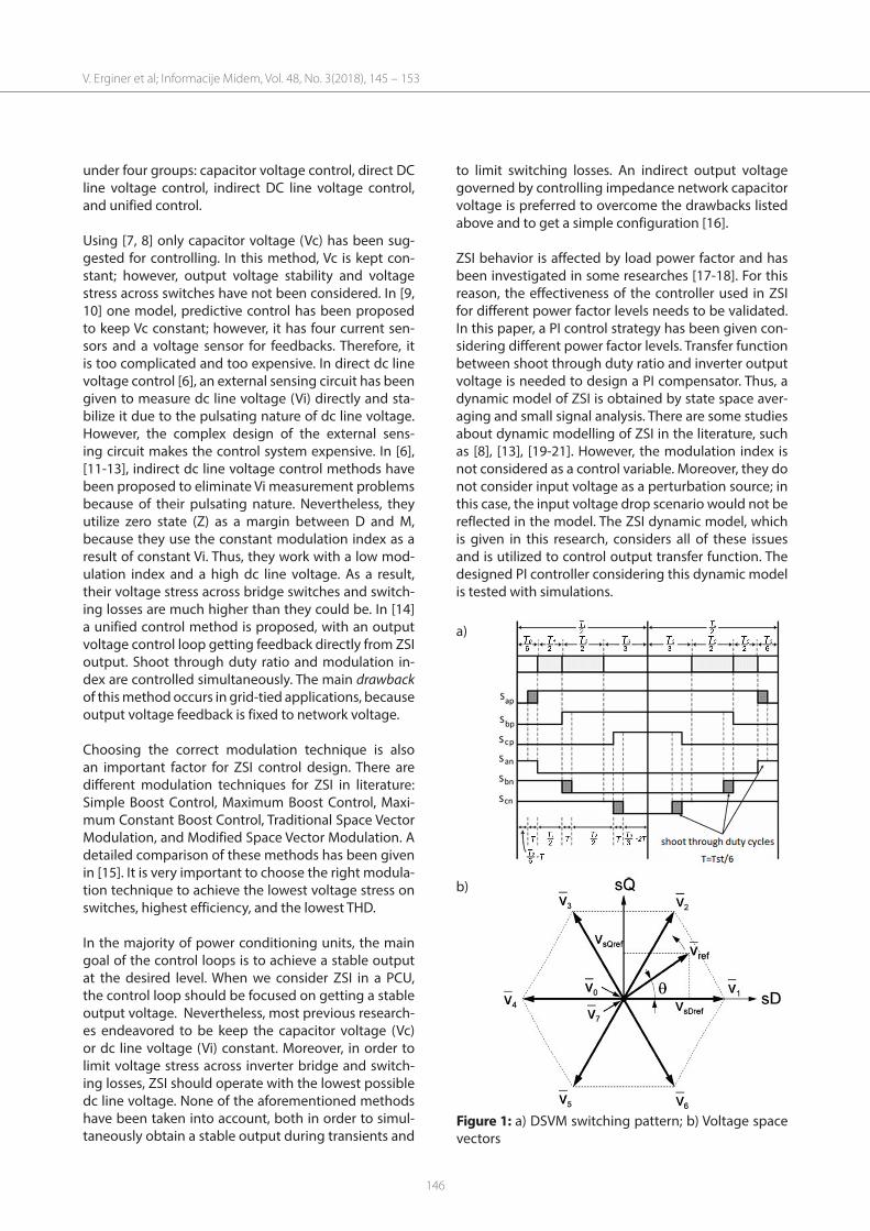
Figure 1: a) DSVM switching pattern; b) Voltage space vectors
b)

147
2 Distributed Space Vector Modulation
The Distributed Space Vector Modulation (DSVM) switching pattern is given in Figure 1. Shoot through duty cycles are divided into six parts, which are settled not only into zero states but also between active states. This results in a well-balanced distribution of shoot through states and thus a better performance can be achieved.
DSVM gives the chance to get the highest DC bus uti-lization, and DSVM allows ZSI output voltage estima-tion with only z-source capacitor voltage feedback. The DSVM scheme can be seen in Figure 1. Related equa-tions are given in (1)-(6).
23k inV V = (1)
_ _
32ref max out peak kV V V
= =
(2)
3peaki
outpeak
V MV = (3)
1M D= − (4)
1peak
ci
VVD
=−
(5)
3peak
cout
VV = (6)
The terms used in these equations are described below.k: voltage space vector number (1,2...6)Vi: ZSI dc line voltageVin: ZSI dc input voltageVref,max: ZSI ac output voltage peak value (reference)Vout: ZSI ac output voltageM: modulation indexD: shoot through duty ratioVc: ZSI impedance network capacitor voltage
As can be seen from (4), no zero state is used in the proposed control method. Thus, it is guaranteed to get the minimum possible dc line voltage and the mini-mum voltage stress to get the desired output voltage level. According to (6), the ZSI output voltage can be estimated by a very simple calculation using only the capacitor voltage feedback. This is a very precious re-lationship because it allows ZSI output voltage control
without output voltage feedback. So, it is possible to control ZSI output voltage indirectly by capacitor volt-age control. It is necessary to achieve control to output transfer function to design a suitable controller. So, this is needed to get a dynamic model of ZSI.
3 Modelling of ZSI
It is essential to get a dynamic model of ZSI to ana-lyze both steady state and transient operation; it is also essential to get a transfer function between shoot through duty ratio and z source capacitor voltage to design a proper controller. However, ZSI has a nonlin-ear characteristic, as can be seen in Figure 2.
Figure 2: Nonlinear relationship between shoot through duty ratio and capacitor voltage boosting ratio
Because of the nonlinear characteristic of ZSI, the sys-tem shall be linearized around an equilibrium point due to utilizing a linear controller. Therefore, the state space averaging method is used to get the ZSI model, and small signal analysis is used to linearize the system around an equilibrium point. Although previous re-searches have ignored the modulation index as a con-trol variable, in this research it is considered a control variable to determine the exact dynamic inverter mod-el. Moreover, it is also essential to consider input volt-age as a perturbation source to get a model for analyz-ing dynamic problems like inverter input voltage drop.
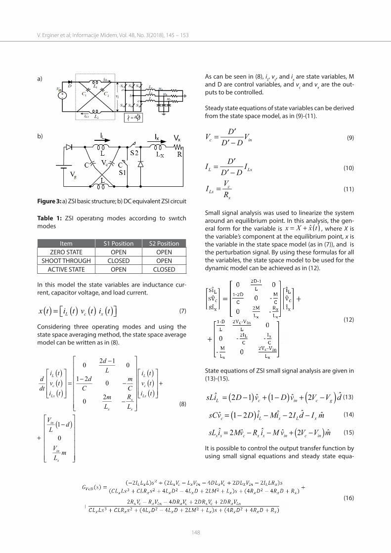
In order to simplify ZSI ac side as a dc load it has been considered ZSI has a balanced load. The circuit diagram can be seen in Figure 3.
Three states are considered while modelling ZSI: shoot through mode, zero voltage vector mode, and active voltage vector mode. These modes can be shown with the proper switch states in Table 1.
V. Erginer et al; Informacije Midem, Vol. 48, No. 3(2018), 145 – 153
148
Table 1: ZSI operatıng modes accordıng to swıtch modes
Item S1 Position S2 PositionZERO STATE OPEN OPEN
SHOOT THROUGH CLOSED OPENACTIVE STATE OPEN CLOSED
In this model the state variables are inductance cur-rent, capacitor voltage, and load current.
( ) ( ) ( ) ( ) L c xx t i t v t i t = (7)
Considering three operating modes and using the state space averaging method, the state space average model can be written as in (8).
(8)
As can be seen in (8), iL, vc, and ix are state variables, M and D are control variables, and vc and vx are the out-puts to be controlled.
Steady state equations of state variables can be derived from the state space model, as in (9)-(11).
c inDV V
D D′ −′= (9)
L LxDI I
D D−′
′= (10)
cLx
x
VIR
= (11)
Small signal analysis was used to linearize the system around an equilibrium point. In this analysis, the gen-eral form for the variable is ( )ˆx X x t= + , where X is the variable’s component at the equilibrium point, x is the variable in the state space model (as in (7)), and is the perturbation signal. By using these formulas for all the variables, the state space model to be used for the dynamic model can be achieved as in (12).
(12)
State equations of ZSI small signal analysis are given in (13)-(15).
( ) ( ) ( ) 2 1 1 ˆˆ ˆ 2ˆL c in c gsLi D v D v V V d= − + − + − (13)
( ) ˆˆ 2 ˆ ˆ1ˆ 2c L x L xsCv D i Mi I d I m= − − − − (14)
( ) 2 2 ˆ ˆˆ ˆ ˆx x c x x in c insL i Mv R i M v V V m= − − + − (15)
It is possible to control the output transfer function by using small signal equations and steady state equa-
Figure 3: a) ZSI basic structure; b) DC equivalent ZSI circuit
a)
b)
(16)
V. Erginer et al; Informacije Midem, Vol. 48, No. 3(2018), 145 – 153
149
tions. The output control transfer function (16) is pro-vided as a third order transfer function.
The derived transfer function has a right half plane (RHP) zero that causes a non-minimum phase response.
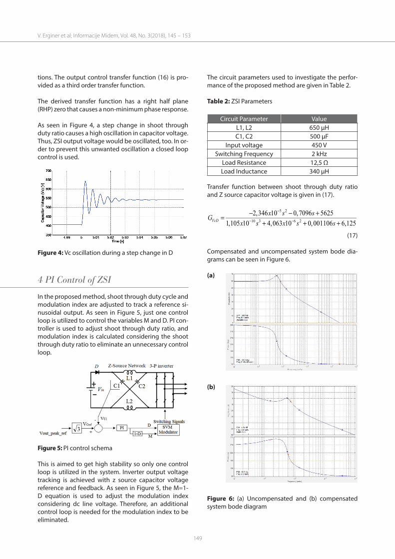
As seen in Figure 4, a step change in shoot through duty ratio causes a high oscillation in capacitor voltage. Thus, ZSI output voltage would be oscillated, too. In or-der to prevent this unwanted oscillation a closed loop control is used.
Figure 4: Vc oscillation during a step change in D
4 PI Control of ZSI
In the proposed method, shoot through duty cycle and modulation index are adjusted to track a reference si-nusoidal output. As seen in Figure 5, just one control loop is utilized to control the variables M and D. PI con-troller is used to adjust shoot through duty ratio, and modulation index is calculated considering the shoot through duty ratio to eliminate an unnecessary control loop.
Figure 5: PI control schema
This is aimed to get high stability so only one control loop is utilized in the system. Inverter output voltage tracking is achieved with z source capacitor voltage reference and feedback. As seen in Figure 5, the M=1-D equation is used to adjust the modulation index considering dc line voltage. Therefore, an additional control loop is needed for the modulation index to be eliminated.
The circuit parameters used to investigate the perfor-mance of the proposed method are given in Table 2.
Table 2: ZSI Parameters
Circuit Parameter ValueL1, L2 650 µHC1, C2 500 µF
Input voltage 450 VSwitching Frequency 2 kHz
Load Resistance 12,5 ΩLoad Inductance 340 µH
Transfer function between shoot through duty ratio and Z source capacitor voltage is given in (17).
5 2
10 3 6 22,346 10 0,7096 5625
1,105 10 4,063 10 0,001106 6,125VcDx s sG
x s x s s
−
− −
− − +=+ + +
(17)
Compensated and uncompensated system bode dia-grams can be seen in Figure 6.
(a)
(b)
Figure 6: (a) Uncompensated and (b) compensated system bode diagram
V. Erginer et al; Informacije Midem, Vol. 48, No. 3(2018), 145 – 153

150
5 Results
The proposed control method is tested with Matlab/Simulink simulations for two different power factor lev-els (PF = 1 and PF = 0,9) to investigate the performance of controller for different kinds of loads. The Simulink diagram of the control system can be seen in Figure 7.
Figure 7: Simulink diagram of the control system
The proposed method is tested for two situations: 1. 11% input voltage drop (450 V to 400 V) at 0,5 sec-
onds.2. 75% load decrease at 0,4 seconds, and then a 75%
load increase at 0,7 seconds.
The results are given in Figures 8-12. As seen in Figure 8, the proposed control method compensates over-shoots and oscillations of the capacitor voltage, as given in Figure 4. Therefore, it contributes to the safety of the system.
Figure 9 (a) and (b) show that when the input voltage decreases, the shoot‐through duty cycle D increases in order to obtain the desired ac output voltage, with a transient regulation. Figure 9 (c) and (d) show that when the load increases or decreases, the shoot-through duty cycle D respectively reduces or increases in order to obtain the desired ac output voltage. Moreover, as can be seen in Figure 10, dc line voltage is increased during input voltage step down so it is not kept con-stant, contrary to previous researches. Figure 11 shows the phase-A output voltage and current. Note that the current is scaled to ten times the actual value to be comparable with the voltage. Fig. 11(a) and (b) shows the output voltage and output current after the input voltage changes. Also, Figure 11(b) and (d) shows the ac voltage and current during the load variation.
The zoomed version of the inductor current and the dc line voltage are shown in Figure 12 to illustrate the impact of the shoot‐through states. It can be observed from this figure that the inductor current is increasing during the shoot‐through states, while dc line voltage is zero because of the short‐circuit of the dc line.
Figure 8: Capacitor voltage (Vc) response for a) 11% input voltage step down (PF=1); b) 75% load change (PF=1); c) 11% input voltage step down (PF=0,9); and d) 75% load change (PF=0,9)
a)
b)
c)
d)
As seen in the figures, the proposed PI control method has a good dynamic performance for both resistive and inductive loads. Control performance is nearly excellent for resistive load, and inverter output voltage becomes stable in half a period during a disturbance. Control performance is also very good for inductive load, and inverter output voltage becomes stable in the 2-3 pe-riod during a disturbance. Contrary to previous works, variable dc line voltage lets the ZSI work with a flexible
V. Erginer et al; Informacije Midem, Vol. 48, No. 3(2018), 145 – 153

151
Figure 9: Shoot Through Duty Ratio (D) response for a) 11% input voltage step down (PF=1); b) 75% load change (PF=1); c) 11% input voltage step down (PF=0,9); and d) 75% load change (PF=0,9)
a)
b)
c)
d)
Figure 10: Dc line voltage (Vi) response for a) 11% input voltage step down (PF=1); b) 75% load change (PF=1); c) 11% input voltage step down (PF=0,9); and d) 75% load change (PF=0,9)
a)
b)
c)
d)
modulation index; therefore, ZSI becomes capable of working with lower voltage stress on switches. Flexible modulation index and SVM lets it work with minimum dc line voltage. Thus, voltage stress on switches is mini-mized.
6 Conclusion
In this research, a dynamic model of ZSI is given. It con-siders both modulation index (M) and shoot through
V. Erginer et al; Informacije Midem, Vol. 48, No. 3(2018), 145 – 153

152
Figure 11: Phase-A output voltage (Vout) and Output current (Iout) response for a) 11% input voltage step down (PF=1); b) 75% load change (PF=1); c) 11% input voltage step down (PF=0,9); and d) 75% load change (PF=0,9)
a)
b)
c)
d)
a)
b)
Figure 12: The zoomed version of a) the dc line voltage (Vi); b) the inductor current (Ii)
duty ratio (D) as control variables; moreover, three operation states (active, zero, and shoot through) are considered for modelling to get a successful model. Considering this dynamic model, a control method based on distributed space vector modulation, which eliminates the drawbacks in the previous researches, is proposed for ZSI. In the proposed method, inverter output voltage is controlled via z source capacitor voltage feedback in order to achieve a high dynamic performance. Furthermore, the proposed method is investigated with a novel approach by considering dif-ferent load power factor levels. Although the proposed method is effective for different loads, research results show that linear control methods are not enough for
systems that have a load power factor range that is too wide. Moreover, very high input voltage oscillations make linear controllers useless because of the transfer function, which is obtained on an equilibrium point. Therefore, nonlinear control systems with a new ap-proach shall be utilized for wide power factor ranges and wide input voltage oscillations variations.
7 Acknowledgement
This work was supported by the Scientific Research Project Department of Yildiz Technical University under Grant 2013-04-02-DOP03.
8 References
1. F. Z. Peng, “Z-Source Inverter”, IEEE Transactions On Industry Applications, vol. 39, no. 2, pp. 504-510, 2003. [Online] Available: http://dx.doi.org/10.1109/TIA.2003.808920
2. Y. P. Siwakoti, F. Z. Peng, F. Blaabjerg, P. C. Loh, G. E. Town, “Impedance-Source Networks for Electric Power Conversion Part I: A Topological Review”, IEEE Transactions On Power Electronics, vol. 30, no. 4, pp. 699-716, 2015. [Online] Available: http://dx.doi.org/10.1109/TPEL.2014.2313746
3. Y. P. Siwakoti, F. Z. Peng, F. Blaabjerg, P. C. Loh, G. E. Town, S. Yang, “Impedance-Source Networks for Electric Power Conversion Part II: Review of Control and Modulation Techniques”, IEEE Trans-actions On Power Electronics, vol. 30, no. 4, pp.
V. Erginer et al; Informacije Midem, Vol. 48, No. 3(2018), 145 – 153

153
1887-1906, 2015. [Online] Available: http://dx.doi.org/10.1109/TPEL.2014.2329859
4. M. M. Bajestan, M. A. Shamsimejad and D. A. Khaburi, “Derivation of AC small signal model and analysis of trans Z-source inverter”, in 23rd Iranian Conference on Electrical Engineering, Tehran, May 2015, pp. 1624-1629. [Online] Available: http://dx.doi.org/10.1109/IranianCEE.2015.7146479
5. A. Florescu, O. Stocklosa, M. Teodorescu, C. Radoi, D. A. Stoichescu, S. Rosu, “The advantages, limita-tions and disadvantages of Z-source inverter”, in IEEE International Semiconductor Conference (CAS), Sinaia, Oct. 2010, pp. 483-486. [Online] Available: http://dx.doi.org/10.1109/SMICND.2010.5650503
6. G. Sen, M. Elbuluk, “Voltage and current pro-grammed modes in control of the Z-source con-verter”, IEEE Trans. Ind. Appl., vol. 46, no. 2, pp. 680–686, 2010. [Online] Available: http://dx.doi.org/10.1109/TIA.2010.2040054
7. X. Ding, Z. Qian, S. Yang, B. Cui, F. Peng, “A PID control strategy for dc-link boost voltage in Z-source inverter”, in IEEE 22nd Annual Aplpied Pow-er Electronics Conference, Anaheim, USA, 2007, pp. 1145–1148. [Online] Available: http://dx.doi.org/10.1109/APEX.2007.357659
8. M. Shen,Q. Tang, F. Z. Peng, “Modeling and con-troller design of the Z-source inverter with in-ductive load”, in IEEE Power Electron. Spec. Conf., Orlando, 2007, pp. 1804–1809. [Online] Available: http://dx.doi.org/10.1109/PESC.2007.4342275
9. W. Mo, P. C. Loh, F. Blaabjerg, “Model predic-tive control for Z-source power converter”, in 8th Int. Conf. on Power Electronics, Jeju, 2011, pp. 3022–3028. [Online] Available: http://dx.doi.org/10.1109/ICPE.2011.5944809
10. M. Mosa, O. Ellabban, A. Kouzou, A. R. Haitham, J. Rodriguez, “Model Predictive Control Applied for Quasi-Z-Source Inverter”, in Applied Power Elec-tronics Conference and Exposition, Long Beach, 2013, pp. 165-169. [Online] Available: http://dx.doi.org/10.1109/APEC.2013.6520202.
11. C. J. Gajanayake, D. M. Vilathgamuwa, P. C. Loh, “Development of a Comprehensive Model and a Multiloop Controller for Z–Source Inverter DG Systems”, IEEE Trans. Ind. Appl., vol. 54, no.4, pp. 2352-2359, 2007. [Online] Available: http://dx.doi.org/10.1109/TIE.2007.894772
12. O. Ellabban, J .V. Mierlo, P. Lataire, “A DSP-based dual-loop peak DC-link voltage control strategy of the Z-source inverter”, IEEE Transactions on Pow-er Electronics, vol. 27, no. 9, pp. 4088-4097, 2012. [Online] Available: http://dx.doi.org/10.1109/TPEL.2012.2189588
13. Y. Liu, B. Ge, H. Abu-Rub, F. Z. Peng, “Control Sys-tem Design of Battery-Assisted Quasi-Z-Source Inverter for Grid-Tie Photovoltaic Power Genera-
tion”, IEEE Transactions On Sustainable Energy, vol. 4, no. 4, pp. 994-1001, 2013. [Online] Available: http://dx.doi.org/10.1109/TSTE.2013.2263202
14. S. Yang, X. Ding, F. Zhang, F. Z. Peng, Z. Qian, “Uni-fied control technique for Z-source inverter”, in IEEE Power Electron. Spec. Conf., Rhodes, 2008, pp. 3236–3242. [Online] Available: http://dx.doi.org/10.1109/PESC.2008.4592452
15. Ö. Girgin, V. Erginer, M. H. Sarul, “Analysis and Comparison of Control Methods of Z-Source Inverters Used in Photovoltaic Systems”, in Pro-ceedings of the World Congress on Electrical En-gineering and Computer Systems and Science (EECSS 2015), Barcelona, July 2015, pp. 148/1-148/11. [Online] Available: http://avestia.com/EECSS2015_Proceedings/files/papers/EEE148.pdf
16. V. Erginer, M. H. Sarul, “A novel control method for Z-source inverters used in photovoltaic systems”, in the 7th IET International Conference on Power Electronics, Machines and Drives (PEMD), Manches-ter, April 2014, pp. 1-5. [Online] Available: http://dx.doi.org/10.1049/cp.2014.0250
17. M. Shen, F. Z. Peng, “Operation Modes and Char-acteristics of the Z-Source Inverter With Small Inductance or Low Power Factor”, IEEE Transac-tions On Industrial Electronics, vol. 55, no. 1, pp. 89-96, 2008. [Online] Available: http://dx.doi.org/10.1109/TIE.2007.909063
18. V. Erginer, M. H. Sarul, “A novel reduced leakage cur-rent modulation technique for Z-source inverter used in photovoltaic systems”, IET Power Electronics, vol. 7, no. 3, pp. 496-502, 2014. [Online] Available: http://dx.doi.org/10.1049/iet-pel.2013.0187
19. P. C. Loh, D. M. Vilathgamuwa, C. J. Gajanayake, Y. R. Lim, C. W. Teo, “Transient modeling and analy-sis of pulse-width modulated Zsource inverter”, IEEE Trans. Power Electron., vol. 22, no. 2, pp. 498–507, 2007. [Online] Available: http://dx.doi.org/10.1109/TPEL.2006.889929
20. J. Liu, J. Hu, L. Xu, “Dynamic modelling and analy-sis of Z source converter-derivation of AC small signal model and design-oriented analysis”, IEEE Trans. Power Electron., vol. 22, no. 5, pp. 1786–1796, 2007. [Online] Available: http://dx.doi.org/10.1109/TPEL.2007.904219
21. M. Forouzesh, Y. P. Siwakoti, F. Blaabjerg, S. Hasan-pour, “Small-Signal Modeling and Comprehensive Analysis of Magnetically Coupled Impedance-Source Converters”, IEEE Transactions On Power Electronics, vol. 31, no. 11, pp. 7621-7641, 2016. [Online] Available: http://dx.doi.org/10.1109/TPEL.2016.2553849
Arrived: 04. 01. 2018Accepted: 23. 05. 2018
V. Erginer et al; Informacije Midem, Vol. 48, No. 3(2018), 145 – 153