Embed Size (px)
Citation preview
Progress In Electromagnetics Research Letters, Vol. 71, 29–36, 2017
A Novel Wideband Phase Shifter Using T- and Pi-Networks
Mohammad H. Maktoomi1, *, Rahul Gupta1,Mohammad A. Maktoomi2, and Mohammad S. Hashmi1
Abstract—In this paper, a wideband differential phase shifter based on modified T- and Pi-networks isproposed. Invoking the even-odd mode analysis in this symmetric phase shifter, closed-form equationsof its S-parameters are derived. The derived equations enable a generic design scheme of the phaseshifter, that is, ideally the phase shifter can be designed for any differential phase requirements. Toillustrate the proposed idea, design parameters for differential phases of 45◦, 60◦, 75◦, 90◦, 105◦ and120◦ are evaluated and tabulated considering a center frequency of 3GHz. Simulation of these examplesusing the Keysight ADS exhibits the intended performance. For validation, a 90◦ phase shifter has beenfabricated and tested. The measurement results show a return loss better that 10 dB, an insertion lossof less than 1 dB, and a ±7◦ of phase deviation from 1.18 GHz to 5.44 GHz, which is equivalent to afractional bandwidth of 142%.
1. INTRODUCTION
Differential phase shifters are commonly employed in wideband phase-array antennas, mobile satellitesystems and measuring instruments, etc. Schiffman [1] introduced a phase shifter which has a main linebuilt around a shorted coupled line and a simple transmission line serves as the reference line. However, itwas based on a strip line that for specific bandwidth requirement, often necessitated very tight coupling.Various improvements over the Schiffman phase shifter using cascade and parallel combination of shortedcoupled line have been introduced [2–4], but again, tight coupling is still required. The implementationof a phase shifter using selectively etching the underneath of the coupled lines and placing a material ofdifferent permittivity to change the even and odd mode impedance values is an interesting idea [5]. Areturn loss better than 10 dB and a bandwidth up to 70% have been achieved by doing so, but this phaseshifter requires extra process step. Phase shifters reported in [6, 7] provide wide bandwidth but thesedesigns also require multilayer fabrication process which increases their fabrication cost and may not becompatible with other part of the circuit. A design using stub loaded line reported in [8] has relativelysmaller insertion loss and could provide a bandwidth up to 82%. Some other interesting designs havebeen reported in literature as well [9–12] and their performance are given at the end of this paper inthe comparison section; majority of them rely on multilayer processing. A technique to utilize singlereference line and multiple main lines to achieve different phase shifts was reported in [13], and canprovide 45% bandwidth with a phase deviation of 5◦ and with an insertion loss up to 0.9 dB. Whilein [14] the main line is formed by changing the position of the stubs and could attain a bandwidthof 55.6% with a return loss up to 0.7 dB considering a phase deviation of 8◦, the multilayer techniquereported in [15] achieves a bandwidth of 112%. A modified version of the Shiffman phase shifter withthe reference line also comprising of a coupled line was reported in [16], while [17] is limited to providingonly 180◦ phase shift.
Received 2 August 2017, Accepted 21 September 2017, Scheduled 9 October 2017* Corresponding author: Mohammad H. Maktoomi ([email protected]).1 Circuit Design & Research Laboratory, IIIT Delhi, New Delhi, India. 2 iRadio Lab, University of Calgary, Calgary, AB T2N 1N4,Canada.
30 Maktoomi et al.
In this paper, we propose a differential phase shifter in which a Pi-network serves as the main line,and a T-network is used as the reference line. The design offers an excellent fractional bandwidth of142% considering a phase deviation of ±7◦, is fully planar and does not require any extra processingstep in the underneath ground plane and therefore, is highly suitable for microstrip implementation.
2. THE PROPOSED PHASE SHIFTER: THEORY AND DESIGN
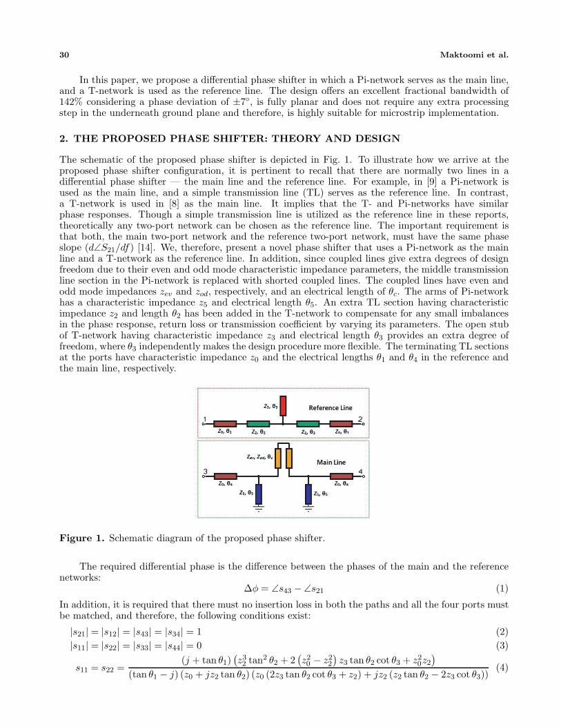
The schematic of the proposed phase shifter is depicted in Fig. 1. To illustrate how we arrive at theproposed phase shifter configuration, it is pertinent to recall that there are normally two lines in adifferential phase shifter — the main line and the reference line. For example, in [9] a Pi-network isused as the main line, and a simple transmission line (TL) serves as the reference line. In contrast,a T-network is used in [8] as the main line. It implies that the T- and Pi-networks have similarphase responses. Though a simple transmission line is utilized as the reference line in these reports,theoretically any two-port network can be chosen as the reference line. The important requirement isthat both, the main two-port network and the reference two-port network, must have the same phaseslope (d∠S21/df) [14]. We, therefore, present a novel phase shifter that uses a Pi-network as the mainline and a T-network as the reference line. In addition, since coupled lines give extra degrees of designfreedom due to their even and odd mode characteristic impedance parameters, the middle transmissionline section in the Pi-network is replaced with shorted coupled lines. The coupled lines have even andodd mode impedances zev and zod, respectively, and an electrical length of θc. The arms of Pi-networkhas a characteristic impedance z5 and electrical length θ5. An extra TL section having characteristicimpedance z2 and length θ2 has been added in the T-network to compensate for any small imbalancesin the phase response, return loss or transmission coefficient by varying its parameters. The open stubof T-network having characteristic impedance z3 and electrical length θ3 provides an extra degree offreedom, where θ3 independently makes the design procedure more flexible. The terminating TL sectionsat the ports have characteristic impedance z0 and the electrical lengths θ1 and θ4 in the reference andthe main line, respectively.
Figure 1. Schematic diagram of the proposed phase shifter.
The required differential phase is the difference between the phases of the main and the referencenetworks:
Δφ = ∠s43 − ∠s21 (1)
In addition, it is required that there must no insertion loss in both the paths and all the four ports mustbe matched, and therefore, the following conditions exist:
|s21| = |s12| = |s43| = |s34| = 1 (2)|s11| = |s22| = |s33| = |s44| = 0 (3)
s11 = s22 =(j + tan θ1)
(z32 tan2 θ2 + 2
(z20 − z2
2
)z3 tan θ2 cot θ3 + z2
0z2
)(tan θ1 − j) (z0 + jz2 tan θ2) (z0 (2z3 tan θ2 cot θ3 + z2) + jz2 (z2 tan θ2 − 2z3 cot θ3))
(4)
Progress In Electromagnetics Research Letters, Vol. 71, 2017 31
s21 = s12 =j2z0z2z3 (j + tan θ1) cot θ3 sec2 θ2
(tan θ1 − j) (z0 + jz2 tan θ2) (z0 (2z3 tan θ2 cot θ3 + z2) + jz2 (z2 tan θ2 − 2z3 cot θ3))(5)
s33 = s44 = − (tan θ4 + j){z20 (zev cot θ5 cot θc − z5) (z5 cot θc + zod cot θ5) + z2
5zevzod cot θc
}(tan θ4 − j) {z0z5 − zev cot θc (z0 cot θ5 + jz5)} {z0 (z5 cot θc + zod cot θ5) + jz5zod} (6)
s43 = s34 =jz0z
25 (tan θ4 + j)
(zev cot2 θc + zod
)(tan θ4 − j) (z0z5 − zev cot θc (z0 cot θ5 + jz5)) (z0 (z5 cot θc + zod cot θ5) + jz5zod)
(7)
∠s21 = tan−1
(tan θ1 cot θ3 sec2 θ2
− cot θ3 sec2 θ2
)
− tan−1
⎛⎜⎜⎝
tan θ1
{z2 tan θ2 + z3 cot θ3
(tan2 θ2 − 1
)} − 2z20 (2z3 tan θ2 cot θ3 + z2)
+2z22 tan θ2 (z2 tan θ2 − 2z3 cot θ3)
z2 tan θ2 + z3 cot θ3
(tan2 θ2 − 1
)+ 2z2
0 tan θ1 (2z3 tan θ2 cot θ3 + z2)−2z2
2 tan θ1 tan θ2 (z2 tan θ2 − 2z3 cot θ3)
⎞⎟⎟⎠ (8)
∠s43 = tan−1
{z0z
25 tan θ4
(zev cot2 θc + zod
)−z0z2
5 (zev cot2 θc + zod)
}
− tan−1
⎧⎪⎪⎨⎪⎪⎩
z20 (zev cot θ5 cot θc − z5) (z5 cot θc + zod cot θ5) − z2
5zevzod cot θc
+z5z0 tan θ4
{z5
(zod − zev cot2 θc
) − 2zevzod cot θ5 cot θc
}z5z0
{z5
(zod − zev cot2 θc
) − 2zevzod cot θ5 cot θc
}+z2
0 tan θ4(z5−zev cot θ4 cot θc)(z5 cot θc+zod cot θ5)+z25zevzod tan θ4 cot θc
⎫⎪⎪⎬⎪⎪⎭ (9)
Since both the lines are symmetric and thus the even-odd mode analysis is invoked and the resultingS-parameters are obtained as mentioned in Eqs. (4)–(9).
In order that both the networks’ phase variations are similar with frequency, an additional conditionon the phase slope of both the networks holds true [14]:
d∠s43
df=
d∠s21
df(10)
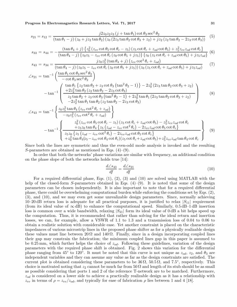
For a required differential phase, Eqs. (1), (2), (3) and (10) are solved using MATLAB with thehelp of the closed-form S-parameters obtained in Eqs. (4)–(9). It is noted that some of the designparameters can be chosen independently. It is also important to note that for a required differentialphase, there could be overwhelming computational burden while enforcing the conditions set by Eqs. (2),(3), and (10), and we may even get some unrealizable design parameters. Since, normally achieving10–20 dB return loss is adequate for all practical purposes, it is justified to relax |S11| requirement(from its ideal value of ∞dB) to enhance the computational speed. Similarly, 0.5 dB–1 dB insertionloss is common over a wide bandwidth, relaxing |S21| form its ideal value of 0 dB a bit helps speed upthe computation. Thus, it is recommended that rather than solving for the ideal return and insertionlosses, we can, for example, allow a VSWR of 1.1 to 1.3 and a transmission loss of 0.04 to 0.06 toobtain a realistic solution with considerable ease. Yet another constraint is placed on the characteristicimpedances of various microstrip lines in the proposed phase shifter as for a physically realizable designthese values must line between 20 Ω and 140 Ω. Finally, since in a design incorporating coupled linestheir gap may constrain the fabrication; the minimum coupled lines gap in this paper is assumed tobe 0.25 mm, which further helps the choice of zod. Following these guidelines, variation of the designparameters with the required phase shift is obtained. Fig. 2 shows this variation for the differentialphase ranging from 45◦ to 120◦. It must be noted that this curve is not unique as zod, z2, and θ3 areindependent variables and they can assume any value as far as the design constraints are satisfied. Thecurrent plot is obtained considering these parameters to be 36 Ω, 50.5 Ω, and 7.5◦, respectively. Thischoice is motivated noting that z2 cannot be much far from 50 Ω and length of its stub should be as smallas possible considering that ports 1 and 2 of the reference T-network are to be matched. Furthermore,zod is considered on a lower side to achieve a practically realizable design as it has a relationship withzev in terms of ρ = zev/zod, and typically for ease of fabrication ρ lies between 1 and 4 [18].
32 Maktoomi et al.
Figure 2. Design parameters of the proposed phase shifter for different phase shifts.
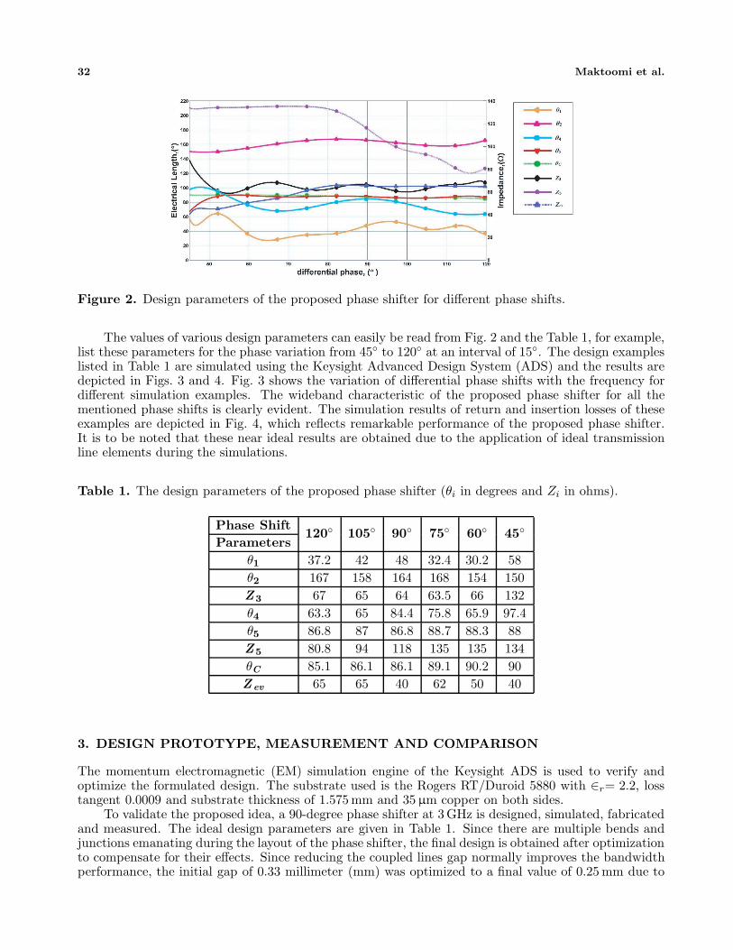
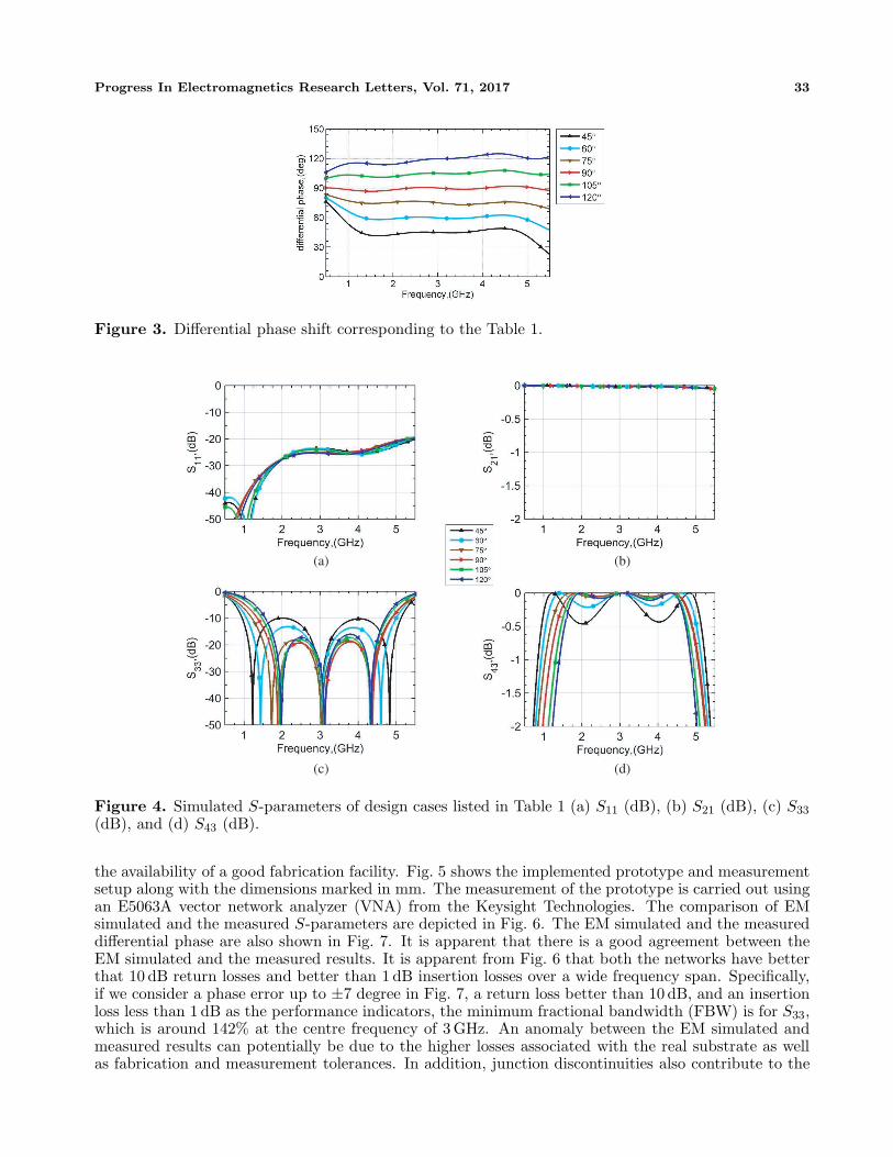
The values of various design parameters can easily be read from Fig. 2 and the Table 1, for example,list these parameters for the phase variation from 45◦ to 120◦ at an interval of 15◦. The design exampleslisted in Table 1 are simulated using the Keysight Advanced Design System (ADS) and the results aredepicted in Figs. 3 and 4. Fig. 3 shows the variation of differential phase shifts with the frequency fordifferent simulation examples. The wideband characteristic of the proposed phase shifter for all thementioned phase shifts is clearly evident. The simulation results of return and insertion losses of theseexamples are depicted in Fig. 4, which reflects remarkable performance of the proposed phase shifter.It is to be noted that these near ideal results are obtained due to the application of ideal transmissionline elements during the simulations.
Table 1. The design parameters of the proposed phase shifter (θi in degrees and Zi in ohms).
Phase Shift120◦ 105◦ 90◦ 75◦ 60◦ 45◦
Parametersθ1 37.2 42 48 32.4 30.2 58θ2 167 158 164 168 154 150Z 3 67 65 64 63.5 66 132θ4 63.3 65 84.4 75.8 65.9 97.4θ5 86.8 87 86.8 88.7 88.3 88Z 5 80.8 94 118 135 135 134θC 85.1 86.1 86.1 89.1 90.2 90Zev 65 65 40 62 50 40
3. DESIGN PROTOTYPE, MEASUREMENT AND COMPARISON
The momentum electromagnetic (EM) simulation engine of the Keysight ADS is used to verify andoptimize the formulated design. The substrate used is the Rogers RT/Duroid 5880 with ∈r= 2.2, losstangent 0.0009 and substrate thickness of 1.575 mm and 35 µm copper on both sides.
To validate the proposed idea, a 90-degree phase shifter at 3 GHz is designed, simulated, fabricatedand measured. The ideal design parameters are given in Table 1. Since there are multiple bends andjunctions emanating during the layout of the phase shifter, the final design is obtained after optimizationto compensate for their effects. Since reducing the coupled lines gap normally improves the bandwidthperformance, the initial gap of 0.33 millimeter (mm) was optimized to a final value of 0.25 mm due to
Progress In Electromagnetics Research Letters, Vol. 71, 2017 33
Figure 3. Differential phase shift corresponding to the Table 1.
(a) (b)
(c) (d)
Figure 4. Simulated S-parameters of design cases listed in Table 1 (a) S11 (dB), (b) S21 (dB), (c) S33
(dB), and (d) S43 (dB).
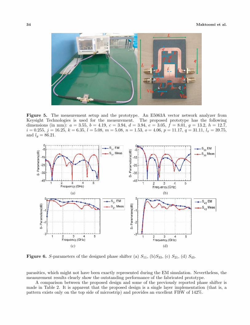
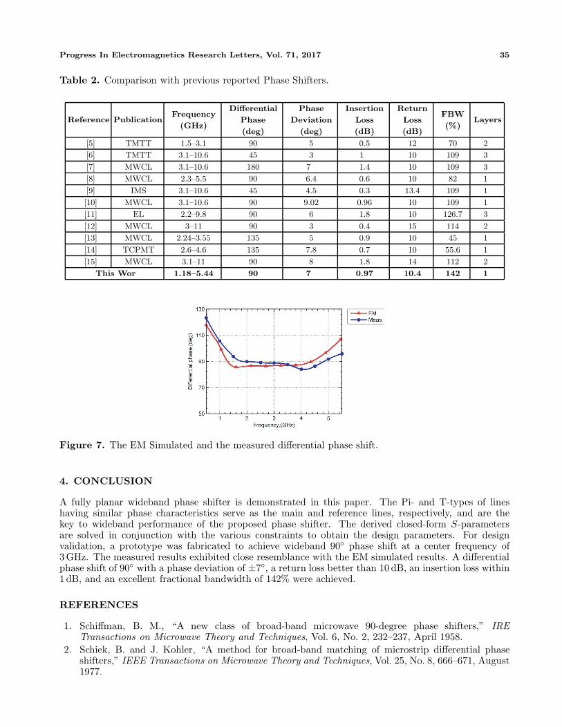
the availability of a good fabrication facility. Fig. 5 shows the implemented prototype and measurementsetup along with the dimensions marked in mm. The measurement of the prototype is carried out usingan E5063A vector network analyzer (VNA) from the Keysight Technologies. The comparison of EMsimulated and the measured S-parameters are depicted in Fig. 6. The EM simulated and the measureddifferential phase are also shown in Fig. 7. It is apparent that there is a good agreement between theEM simulated and the measured results. It is apparent from Fig. 6 that both the networks have betterthat 10 dB return losses and better than 1 dB insertion losses over a wide frequency span. Specifically,if we consider a phase error up to ±7 degree in Fig. 7, a return loss better than 10 dB, and an insertionloss less than 1 dB as the performance indicators, the minimum fractional bandwidth (FBW) is for S33,which is around 142% at the centre frequency of 3 GHz. An anomaly between the EM simulated andmeasured results can potentially be due to the higher losses associated with the real substrate as wellas fabrication and measurement tolerances. In addition, junction discontinuities also contribute to the
34 Maktoomi et al.
Figure 5. The measurement setup and the prototype. An E5063A vector network analyzer fromKeysight Technologies is used for the measurement. The proposed prototype has the followingdimensions (in mm): a = 3.55, b = 4.19, c = 3.94, d = 3.94, e = 3.05, f = 8.01, g = 13.2, h = 12.7,i = 0.255, j = 16.25, k = 6.35, l = 5.08, m = 5.08, n = 1.53, o = 4.06, p = 11.17, q = 31.11, lx = 39.75,and ly = 86.21.
(a) (b)
(c) (d)
Figure 6. S-parameters of the designed phase shifter (a) S11, (b)S33, (c) S21, (d) S43.
parasitics, which might not have been exactly represented during the EM simulation. Nevertheless, themeasurement results clearly show the outstanding performance of the fabricated prototype.
A comparison between the proposed design and some of the previously reported phase shifter ismade in Table 2. It is apparent that the proposed design is a single layer implementation (that is, apattern exists only on the top side of microstrip) and provides an excellent FBW of 142%.
Progress In Electromagnetics Research Letters, Vol. 71, 2017 35
Table 2. Comparison with previous reported Phase Shifters.
Reference PublicationFrequency
(GHz)
Differential
Phase
(deg)
Phase
Deviation
(deg)
Insertion
Loss
(dB)
Return
Loss
(dB)
FBW
(%)Layers
[5] TMTT 1.5–3.1 90 5 0.5 12 70 2
[6] TMTT 3.1–10.6 45 3 1 10 109 3
[7] MWCL 3.1–10.6 180 7 1.4 10 109 3
[8] MWCL 2.3–5.5 90 6.4 0.6 10 82 1
[9] IMS 3.1–10.6 45 4.5 0.3 13.4 109 1
[10] MWCL 3.1–10.6 90 9.02 0.96 10 109 1
[11] EL 2.2–9.8 90 6 1.8 10 126.7 3
[12] MWCL 3–11 90 3 0.4 15 114 2
[13] MWCL 2.24–3.55 135 5 0.9 10 45 1
[14] TCPMT 2.6–4.6 135 7.8 0.7 10 55.6 1
[15] MWCL 3.1–11 90 8 1.8 14 112 2
This Wor 1.18–5.44 90 7 0.97 10.4 142 1
Figure 7. The EM Simulated and the measured differential phase shift.
4. CONCLUSION
A fully planar wideband phase shifter is demonstrated in this paper. The Pi- and T-types of lineshaving similar phase characteristics serve as the main and reference lines, respectively, and are thekey to wideband performance of the proposed phase shifter. The derived closed-form S-parametersare solved in conjunction with the various constraints to obtain the design parameters. For designvalidation, a prototype was fabricated to achieve wideband 90◦ phase shift at a center frequency of3GHz. The measured results exhibited close resemblance with the EM simulated results. A differentialphase shift of 90◦ with a phase deviation of ±7◦, a return loss better than 10 dB, an insertion loss within1 dB, and an excellent fractional bandwidth of 142% were achieved.
REFERENCES
1. Schiffman, B. M., “A new class of broad-band microwave 90-degree phase shifters,” IRETransactions on Microwave Theory and Techniques, Vol. 6, No. 2, 232–237, April 1958.
2. Schiek, B. and J. Kohler, “A method for broad-band matching of microstrip differential phaseshifters,” IEEE Transactions on Microwave Theory and Techniques, Vol. 25, No. 8, 666–671, August1977.
36 Maktoomi et al.
3. Brown, W. J. and J. P. Starski, “A broad-band differential phase shifter of novel design,” IEEEMTT-S International Microwave Symposium Digest, Vol. 3, 1319–1322, 1999.
4. Quirarte, J. L. R. and J. P. Starski, “Novel Schiffman phase shifters,” IEEE Transactions onMicrowave Theory and Techniques, Vol. 41, No. 1, 9–14, January 1993.
5. Guo, Y., Z. Zhang, and L. Ong, “Improved wideband Schiffman phase shifter,” IEEE Transactionson Microwave Theory and Techniques, Vol. 54, No. 3, 1196–1200, March 2006.
6. Abbosh, A. M., “Ultra-wideband phase shifters,” IEEE Transactions on Microwave Theory andTechniques, Vol. 55, No. 9, 1935–1941, September 2007.
7. Guo, L. and A. M. Abbosh, “Phase shifters with wide range of phase and ultra-widebandperformance using stub-loaded coupled structure,” IEEE Microwave and Wireless ComponentsLetters, Vol. 24, No. 3, 167–169, March 2014.
8. Zheng, S. Y., W. S. Chan, and K. F. Man, “Broadband phase shifter using loaded transmissionline,” IEEE Microwave and Wireless Components Letters, Vol. 20, No. 9, 498–500, September 2010.
9. Tang, X. and K. Mouthaan, “Design of a UWB phase shifter using shunt λ/4 stubs,” IEEE MTT-SInternational Microwave Symposium Digest, 1021–1024, June 2009.
10. Yeung, S. H., Z. Mei, T. K. Sarkar, and M. Salazar-Palma, “Design and testing of a single-layermicrostrip ultrawideband 90 differential phase shifter,” IEEE Microwave and Wireless ComponentsLetters, Vol. 23, No. 3, 122–124, March 2013.
11. Wang, J., Z. Shen, and L. Zhao, “UWB 90◦ phase shifter based on broadside coupler and T-shapedstub,” IET Electronics Letters, Vol. 52, No. 25, 2048–2050, December 2016.
12. Abbosh, A. M., “Broadband fixed phase shifters,” IEEE Microwave and Wireless ComponentsLetters, Vol. 21, No. 1, 22–24, January 2011.
13. Pu, X. Y., S. Y. Zheng, J. Liu, Y. Li, and Y. Long, “Novel multi-way broadband differential phaseshifter with uniform reference line using coupled line structure,” IEEE Microwave and WirelessComponents Letters, Vol. 25, No. 3, 166–168, March 2015.
14. Xu, B. W., S. Y. Zheng, and Y. M. Pan, “A universal reference line-based differential phaseshifter structure with simple design formulas,” IEEE Transactions on Components, Packaging andManufacturing Technology, Vol. 7, No. 1, 123–130, January 2017.
15. Wang, Y., M. E. Bialkowski, and A. M. Abbosh, “Double microstrip-slot transitions for broadbandmicrostrip phase shifters,” IEEE Microwave and Wireless Components Letters, Vol. 22, No. 2,58–60, February 2012.
16. Zhang, W., Y. Liu, Y. Wu, W. Wang, M. Su, and J. Gao, “A modified coupled-line Schiffmanphase shifter with short reference line,” Progress In Electromagnetics Research C, Vol. 54, 17–27,2014.
17. Wu, Y., L. Yao, W. Wang, and Y. Liu, “A wide-band 180-degree phase shifter using a pair ofcoupled-line stubs,” IEEE International Symposium on Antennas and Propagation & USNC/URSINational Radio Science Meeting, 240–241, July 2015.
18. Bai, Y.-F., X.-H. Wang, C.-J. Gao, Q.-L. Huang, and X.-W. Shi, “Design of compact quad-frequency impedance transformer using two-section coupled line,” IEEE Transactions on MicrowaveTheory and Techniques, Vol. 60, No. 8, 2417–2423, August 2012.