Embed Size (px)
Citation preview

1
A Programmable 210 µV Offset Rail-to-Rail
GM–C Filter H. Pooya Forghani-zadeh1, Student Member, IEEE, and Gabriel A. Rincón-Mora2, Senior Member, IEEE
1,2 Texas Instruments, Inc. 2Georgia Tech Analog, Power, and Energy ICs Lab
Abstract— Low input-referred offset performance and linearity in analog filters are critical design parameters, yet transistor mismatch limitations are a severe hindrance. Programmability is also a feature of growing significance because high performance state-of-the-art systems must adapt on-the-fly to various operating conditions, as is the case in battery-operated electronics where systems traverse through idle, alert, and high performance modes in an effort to conserve energy and extend battery life. This paper presents a continuous and programmable first-order GM-C filter with sub-milli-Volt offset performance. Low offset is achieved by auto-zeroing and continuity by ping-ponging between two transconductors, all under the construct of a compact and bandwidth-efficient circuit topology. The proposed GM-C circuit was fabricated with AMI’s 0.5-µm CMOS process technology and achieved an input-referred offset of less than 210 µV, hand-over glitches of less than 40 mV, and 57 dB of linearity over the rail-to-rail input span for a lithium-ion battery supply range of 3 to 4.2 V. The bandwidth and gain of the filter were programmable from 1.1 to 6.5 kHz and 1.27 to 29.1 V/V, respectively, both with better than 3.2% resolution.
Index Terms— GM-C filter, programmable, low offset, auto-zero, ping pong, linearity, rail-to-rail, current sensing.
I. INTRODUCTION ow-offset performance in analog filters can be as important as their frequency filtering properties, as is the
case in analog sensors like temperature and capacitive sensing applications [1-2] and instrumentation amplifiers [3-10], where both the DC and ac portions of the signal carry important information. When sub-milli-Volt input-referred offsets are required, increasing the dimensions of critically matched CMOS transistors is often impractical, if not insufficient, because of their inherent offsets and implied bandwidth tradeoffs (i.e., larger devices achieve better matching performance but in the process introduce larger parasitic capacitors), which is why dynamic offset cancellation is so popular. And given the analog nature and accuracy requirements of many applications, these dynamic solutions must also be continuous, that is, capable of filtering the signal linearly with time. Unfortunately, dynamic (i.e., switching) schemes necessarily introduce undesired transient glitches to the system. A few milli-Volts glitch at the input of a high-speed high-resolution comparator, for instance, may inadvertently trigger unexpected transitions and therefore degrade the noise and jitter performance of the overall system.
Tuning the gain and bandwidth of analog filters is also increasingly important in a wide range of applications, from
receiver radio-frequency (RF) filters, where the filter’s bandwidth must match the frequency of the received signal to discern the desired signal from noise, to switching power supply circuits, where a filter is tuned to accurately sense the inductor and therefore the output current. State-of-the-art current-sensing filters for switching supply circuits, in fact, are discrete and cumbersome to program (gain and bandwidth parameters are tuned manually with off-chip resistors and capacitors) [11-12]. An on-chip programmable and continuous low offset GM-C integrated circuit (IC) that meets the accuracy and low glitch requirements of a current-sensing filter for switching power supply applications, particularly a step-down DC-DC converter, as shown in Fig. 1, is therefore proposed [11].
MH
MLL
VLoad
Vin+
RESR
VSupply
IL
gm
RC
Vo=αΙ L
GM-C Filter
CoILoad
Vin-+
-
VSupply
0
Fig. 1. Programmable and continuous low offset GM-C filter for current
sensing in switching supply applications.
The filter is comprised of programmable, auto-zeroed, ping-ponged transconductor GM; adjustable resistor R; and bandwidth-setting capacitor C. The voltage across inductor L and its equivalent series resistor (ESR) is an indicator of the output current (current flowing through L), but its value is low because ESR is typically only a few milli-Ohms, which is why low offset performance is required. The bandwidth of the GM-C filter is “tuned” (“programmed”) to match the process-dependent cut-off frequency of the L-ESR path, thereby canceling the frequency dependence of the measured output (Vo) and ascertaining both DC and ac current information [12-13]. While this cut-off frequency is only a few kilo-Hertz, a single pole response must exist and extend through several decades of frequency, requiring all parasitic poles and zeros to reside well above the frequency range of the system, which can easily exceed 10 MHz. Linearity is also critical for
L

2
accuracy over the entire input voltage range, which includes both supply rails because the non-inverting input of the filter traverses from ground to input supply VSupply.
A continuous and tunable first-order GM-C filter with sub-milli-Volt offset performance is presented and experimentally validated in this paper. A review of dynamic offset cancellation techniques within the context of continuous low offset operation is offered in Section II. Section III introduces and discusses the proposed GM-C filter and Section IV details the particulars of the circuit. Experimental results are then presented in Section V and conclusions drawn in Section VI.
II. OFFSET-CANCELLATION TECHNIQUES Real transistors, in spite of being fabricated with the same
process, near one another, surrounded by similar devices, and in the same orientation, suffer from threshold-, mobility-, and geometry-induced mismatch effects, the end result of which is undesired DC offsets in analog circuit applications [3]. In CMOS process technologies, for instance, threshold voltage and mobility mismatches of supposedly identical devices are inversely proportional to active area, which is why larger devices are normally selected in low offset applications. However, when sub-milli-Volt input-referred offsets are required, such as in precision analog sensor applications, increasing the dimensions of critically matched CMOS components is not practical and dynamic offset-cancellation circuit techniques become necessary [3].
State-of-the-art dynamic offset-cancellation circuits generally fall in one of two categories: auto-zero (AZ) and chopper [3-10]. Auto-zeroing is performed in two phases, the sampling phase where the offset is measured and the processing phase when the offset is subtracted (cancelled) and the input signal is processed. The chopper, on the other hand, periodically switches the polarity of the offset at relatively high frequencies and therefore, on the average, cancels the DC offset of the circuit. In practical terms, a modulator and a demodulator (both at the same chopping frequency) are placed at the front and back ends of a high offset amplifier and a low pass filter at the output. As a result, the input is modulated to high frequencies, but not the DC offset of the amplifier, so that when the output of the amplifier is demodulated back to broadband frequencies, the DC offset is modulated to high frequencies, beyond the pass-band of the low pass filter, canceling in the process the effects of DC offsets.
Although both chopper and auto-zero schemes cancel DC offsets, their time-domain and frequency responses differ. Chopper schemes, for instance, are continuous in time, unlike auto-zeroed amplifiers where information is processed only at discrete times. The signal bandwidth of an auto-zeroed amplifier, on the other hand, is not necessarily limited by auto-zeroing but by the amplifier itself, whereas the signal bandwidth of a chopper amplifier is constrained to half the chopping frequency to prevent the offset from aliasing back into the signal bandwidth during the demodulation phase. What is more, the chopping frequency is limited to several kilo-Hertz because its offset-canceling features are mitigated by clock feed-through and coupling-induced offsets [3]. As a
result, since the input of the filter in current-sensing applications for switching supply circuits can pulse up to a few mega-Hertz and the sensing bandwidth must therefore exceed it by at least a decade, auto-zeroing is preferred. Table 1 summarizes and compares these features.
Table 1. Summary of dynamic offset cancellation techniques.
Chopper Auto Zero Modulates and filters DC offset Samples and subtracts offset
Continuous Discontinuous Higher noise reduction Lower noise reduction
Low Bandwidth (BW < 0.5fChop) High Bandwidth
Continuity in auto-zeroed amplifiers can be achieved by adopting ping-pong and/or feed-forward architectures [3], although both at the cost of complexity, area, and power. In the former, while one amplifier is sensing and measuring its offset, another is processing the signal [6-8]. The operation is then reversed to allow the amplifier that was previously processing the signal to now sense and measure its offset. In practice, noise in the form of transient spikes (glitches) is introduced at the output when the output is disconnected from one amplifier and connected to the other. In feed-forward implementations [9-10, 14-15], an error amplifier is designed and dedicated to continually cancel and compensate the offset of the processing amplifier, thereby avoiding the switching that occurs in the ping-pong strategy. The offset-nulling amplifier is itself auto-zeroed and its output, which tunes the main amplifier, is sampled and held across a capacitor. Feed-forward unfortunately suffers from intermodulation effects between the auto-zero clock frequency and the input signal [14-15], which results in signal distortion. The main disadvantage of this technique, however, within the context of general GM-C filters, is lack of versatility because negative feedback around the processing amplifier is necessary to continually supply a sample of the offset across its input terminals without changing its connectivity, which is why ping pong is often times preferred. Table 2 summarizes and compares ping-pong and feed-forward strategies.
Table 2. Summary of continuous-time auto-zero techniques.
Ping Pong Feed Forward Higher glitch content Lower glitch content
Used in open- and closed-loop amplifiers
Only used in closed-loop, negative feedback amplifiers
No intermodulation effects Intermodulation effects
III. PROPOSED LOW OFFSET GM-C FILTER The proposed continuous low offset GM-C filter, as
illustrated in Fig. 2, is comprised of two well-matched, auto-zeroed, ping-ponging dual-input summing transconductors (i.e., GM1 and GM2); two offset-programming capacitors for each transconductor (i.e., Ch1-, Ch1+, Ch2-, and Ch2+); a single bandwidth-setting capacitor C; gain setting resistor R; and non-overlapping clock signals φ and φn. The non-overlapping feature is implemented to prevent various cross-wiring events. Input voltage Vref, against which filter output voltage Vo is referenced, is used as a virtual ground (ac ground). Finally, as in all ping-pong schemes, while one transconductor processes

3
the input signal, the other one auto-zeroes.
R
Vo
Vref
Ch1-
Ch2-
C
GM1
GM2
+
-+
ϕ
Ch1+
+
-+
Vo1
Vo2
Vaux1-
Vaux2-
Vref
Vid
ϕ
ϕϕnϕϕn
ϕn
ϕ
ϕn
ϕ
ϕ
ϕn
ϕn
-Ch2+
Vref ϕn
-
a
a
Fig. 2. Proposed ping-pong GM-C filter with two auto-zeroing summing
transconductors.
The difference in the proposed scheme is that a summing comparator is used to program and cancel the offset by dedicating an input differential pair to the input signal and another to subtract (i.e., cancel) the offset. The key advantage to this configuration is that the large holding capacitor is de-coupled from the high bandwidth path, that is, not connected to the input ac-signal path and therefore not bandwidth-limiting the signal. A large holding capacitor is desirable because it reduces clock feed-through and charge injection, consequently improving offset cancellation performance [3], all without adversely affecting bandwidth.
A. Offset Cancellation The Norton equivalent circuit of the summing
transconductor, as shown in Fig. 3(a), is composed of two voltage-dependent current sources Vidgm and Vidagma, where gm is the main input-to-output and gma is the auxiliary input-to-output transconductances, Vid is the differential voltage applied to the main input, and Vida is the differential voltage applied to the auxiliary input. The equivalent circuit also includes output resistance Ro and voltage source VUnloaded, which is the unloaded (i.e., open-circuit) output voltage of an ideal (i.e., perfectly matched) transconductance GM cell when its input pairs are short-circuited.
In the programming phase (Fig. 3(b)), the main input pair is short-circuited and the auxiliary pair connected in unity-gain configuration, forcing its output to superimpose the overall offset of the transconductor on programming capacitor Ch-:
( )[ ]ma
mos1os2ref
oma
omos1maos2ref-aux g
gVVVRg1
RgVgVVV ++≈+
++≈ , (1)
where Vh is the voltage across holding capacitor Ch, Vos1 and Vos2 are the offsets of the main and auxiliary ports, and gmaRo is the loop gain, which is designed to be much higher than one (i.e., Ro is large). In ping-ponging the circuit to the processing phase, the stored offset is subtracted from the input by breaking the unity-gain feedback loop, allowing the stored offset voltage to remain across the auxiliary input pair, and
connecting the input signal across the main input pair (Fig. 3(c)),
( ) ( )( )( )( ) ( )
( )
( )( ) ( )( )
( )R||RgggVV
R||RgVR||RgV
R||Rg
ggVVV
gVVVgVV
R||RgVVVVgVVV
omm
mainjid
omainjomid
oma
ma
mos1os2ref
mainjos2refmos1id
oma-auxinjos2refmos1ido
⎟⎟⎠
⎞⎜⎜⎝
⎛⎟⎟⎠
⎞⎜⎜⎝
⎛+=
+≈
⎥⎥⎥
⎦
⎤
⎢⎢⎢
⎣
⎡
⎟⎟⎠
⎞⎜⎜⎝
⎛++−
++++
=
−++++=
, (2)
where Vinj is the clock feed-through and charge injection voltage effects of offset storage switches S1 and S2. Left-ver Vinj errors are reduced by designing gma/gm to be small.
VNatural
(b)
Vo1
Vid=0
R
Vo
C
Vref(c)
Vid
Phase 1: Program
S1 S2
MainInputs
Vid
Io
gmaVida
Vida
(a)
Ro
IoAuxilirayInputs -
+
+-
-+
+-
Ch+
Vref
Ch-
Vos1
Vos2
Vo1-+
+-
Ch+
Ch-
Vos1
Vos2
gmVid
Phase 2: Process
a
a
a
GM
GM
GM
Vaux-
Vaux-
Fig. 3. Summing transconductor’s (a) Norton-equivalent model and respective
(b) offset programming and (c) signal processing phases.
The matching accuracy of the foregoing circuit, as with all dynamic offset-cancellation techniques, is limited by feed-through and charge injection Vinj, which can be reduced (i.e., shunted), but not eliminated, by employing differential hold capacitors and switches [3] and increasing the size of holding capacitors Ch+ and Ch-. The remaining input-referred offset of the main pair is
( )
os2om
os1oma
Unloadedrefomaom
injm
main-res
VRg1V
Rg1
V-VRgRg
1VggV
⎟⎟⎠
⎞⎜⎜⎝
⎛+⎟⎟
⎠
⎞⎜⎜⎝
⎛+
⎟⎟⎠
⎞⎜⎜⎝
⎛+⎟⎟
⎠
⎞⎜⎜⎝
⎛≈
, (3)
where VUnloaded is not necessarily equal to Vref. VUnloaded is in

4
fact dependent on circuit topology and supply and input common-mode voltage through supply- and common-mode rejection ratios CMRR and PSRR. As a result, because of finite values of CMRR and PSRR, remaining offset Vres_in varies slightly with changes in supply and common-mode input voltages, even after the VUnloaded error term is substantially attenuated by gmRogmaRo.
B. Output Transient Glitches When the output is ping-ponged from one summing
transconductor to the other, transient glitches occur because their respective output voltages are not necessarily equal; in other words, their outputs are uncorrelated during a switching handover event. To study the transitional glitches, a transition from when first transconductor GM1 is in the signal path to the state where second transconductor GM2 is in the signal path is illustrated in Fig. 4. Before the transition (Fig. 4(a)), GM-C filter output voltage Vo is equal to GM1 output voltage Vo1 and, after the ping-pong transition (Fig. 4(b)), the GM-C filter output follows GM2 output voltage Vo2. Before the transition, Vo1 is a function of transconductance, bandwidth (i.e., settling behavior), and input voltage (i.e., Vo1 = Vid·Gain) whereas Vo2 is independent of input voltage and close to the reference voltage (Vref) used in the programming phase of the offset cancellation sequence, assuming initial offset values are in milli-Volts and much smaller than Vref. As a result, at the transition, Vo2 is not related to the input signal and may therefore be off from its desired target value when connected to the signal path.
Just after Gm2 is connected in the signal path, the output capacitor charge redistributes and sets the output voltage to somewhere between Vo1 and Vo2, causing an instantaneous error of ΔVglitch (Fig. 4(c)). After the transition, the circuit corrects the systematic handover glitch disturbance, that is, the output voltage converges to its target value, at a rate determined by the circuit’s bandwidth, which is in turn a function of R, C, and the parasitic switch-on resistances and capacitances present at the output and the transconductor’s output impedance. These impedances can be lumped and modeled by a single equivalent low frequency pole (1/REqCEq), the transient response of which induces a momentary error voltage just past the switching transition point:
u(t)eΔVV CRt
GlitchErrorEqEq ⎟⎟
⎠
⎞
⎜⎜
⎝
⎛−
= , (4)
where ΔVglitch is the instantaneous glitch. The value of ΔVGlitch can be quantified by investigating the
charge redistribution during the ping-pong transition time. Just before the transition, Vo is equal to Vo1, which is a function of the input voltage (i.e., Vo = Vo1 = {Vin+-Vin-}·Gain) whereas Vo2, which is at this point disconnected from the output, is close to Vref (i.e., GM2’s output parasitic capacitor Cp2 is charged to Vref), assuming its initial milli-Volt offset voltage is much smaller than Vref, which is on the order of Volts. During a handover event, output capacitor C and resistor R are first disconnected from Vo1 and GM2’s negative auxiliary input disconnected from Vo2, and then, C and R are connected to
Vo2; in other words, Cp2 and C are connected together. Charge is therefore redistributed across these two capacitors, keeping the total charge equal before and after the transition:
( ) ( )( ) ( )glitchop2glitchrefo
refp2refo
ΔVVCΔVVVCVCVVC
+++−=
+−. (5)
As a result, the instantaneous output voltage glitch is
( )orefp2
p2glitch VV
CCC
ΔV −⎟⎟⎠
⎞⎜⎜⎝
⎛
+= . (6)
Vo1Vo2
ΔVGlitch Vo
Vo2
Cp2
Vid Vo1
Cp1
Ch1-
Vo
C R
Process
Process
Program
Program
Vref
(a) (b)
(c)
Ch2-
+-+-
+-+-
Vref
Vref
Vo1
Cp1
Ch1-
+-+-Vref
Vo2
Cp2
Ch2-
VoVid
C
Vref
+-+-Vref
R
aGM1 GM1
GM2 GM2
a
a a
Fig. 4. Glitch performance: (a) GM1 in signal path, (b) GM2 in signal path, and
(c) transient response.
Since output capacitor C is much larger than parasitic capacitor Cp2, output glitches are relatively small. For a 60 pF filter capacitor and a 1.33 pF parasitic capacitor combination, for instance, and 0.8 V worst-case difference between Vref and Vo (Vo = Vid·Gain), the glitches are theoretically limited to 17 mV. Most of these glitches could be considerably reduced if a more complex set of clocking signals were to be generated that would allow the auto-zeroed comparator to settle to its processed value before connecting it to the output, but the increase in complexity is not desirable in the foregoing application. Switch-on parasitic resistances and gate-drain and -source capacitances further degrade the response with clock feed-through and charge-injection noise, but their effects are overwhelmed by the handover glitches. Similarly, random 1/f, shot, and thermal noise is also overwhelmed by these systematic glitches, especially since auto-zeroing cancels the low frequency components of the random noise and the GM cell’s low filter bandwidth, which is on the order of a few kHz, filters out the higher frequency portion [3].

5
IV. CIRCUIT DESIGN
A. Programmable Transconductance In the switching supply circuit shown in Fig. 1, the GM-C
filter must be programmable and highly linear across the rail-to-rail input voltage range. Since the non-inverting input swings from the positive to the negative supply every period, a variation in transconductance (Δgm) in these two states translates to a systematic input-referred offset error voltage (Vos_gm),
idm
mid
m
m
m
oos_gm V
gΔgV
RgRΔg
RgΔVV ⎟⎟
⎠
⎞⎜⎜⎝
⎛=== , (7)
where Vid is the differential voltage applied to the transconductor. As a result, because polysilicon resistors are many times more linear than transistors and the non-inverting input of the transconductor is connected to a low impedance node (i.e., connected to a source capable of supplying current), a wide input voltage range resistor-dependent current conveyor [16-18], as shown in Fig. 5, can be used in place of a traditional differential pair transconductor. The input terminals of amplifier Aint are virtually short-circuited because of negative feedback and the resulting current flowing through series resistor R1 (IR1) is therefore proportional to the differential input voltage applied to the GM-C cell (Vid),
1
idR1 R
VI = . (8)
This current is then mirrored to the output by current mirror M1-M2, ultimately defining the transconductance to
11
id
idid
om R
KRKV
V1
VIg =⎟⎟
⎠
⎞⎜⎜⎝
⎛=≡ , (9)
where K is a digitally programmable current-mirror gain. To add the auxiliary pair needed for the auto-zero feature illustrated in Figs. 2 and 3, a separate and more traditional transconductor is connected directly to the output (gma).
-
+-
+vo
Ib KIb
I1
M1 M2
M3 M4
(W/L)
gma
K(W/L)
R1
Ib2
I2
I3 I4
VG
Aint
CcVid
Vida+
-
idamaid1
o VgVRKI +=
Vin+
Vin-
Fig. 5. Linear, dual-input, rail-to-rail transconductance cell (K is tunable).
To ensure M3 is operating in the saturation region (i.e., ensure the shunt-feedback loop is properly biased), bias current Ib is fed into M3 and the feedback loop around M1, M3, and M4 (Ib2 biases M4) forces the gate voltage of M1 to the exact value necessary to sink Ib and IR1, which is another way of saying M1, M3, and M4 comprise a current mirror where the drain and gate voltages of M1 are decoupled. Additionally, having a constant bias current flowing through M1 also allows the circuit to process both positive- and negative-flowing IR1 currents, that is, process bidirectional currents. Since the current conveyor circuit is highly linear, the overall linearity
-
+
Vo
M1 M2
M3 M4
(W/L)
d6-d0
K(W/L)
AdjustableCurrentMirror
R1
vG
AintCc
Io
M20
...
M26
VB1
PaP1
12µA
PbP2 P26
P20
…Vb2
a+ a-
d6d6n
d6-d0
K(W/L)
-
+
-
+A2
d6d6n
6µA
Na Nc Nd Nb)444( )
444(
)443()
443(
Auxilliary Port
AdjustableCurrentSource
Vid
12µA
100µA
Fig. 6. Full schematic of the GM cell.
6
of the circuit is dependent on the mirror, which is why bias current Ib is designed to be significantly higher than IR1 (noise and quiescent power are sacrificed for this). Because this current is amplified by the programmable-gain mirror, an equally amplified current is fed to the output of the mirror to ensure Io is free of any bias current.
The gate of M4 is high impedance and is therefore the gain- and bandwidth-setting node of the current-mirror’s controlling feedback loop. Compensation capacitor Cc ensures the bandwidth-setting pole is at sufficiently low frequencies to prevent parasitic high frequency poles from compromising stability. The unity-gain frequency of this loop, however, adds a parasitic high frequency pole to the signal-flowing path (Vid to Io) approximately at its gain-bandwidth product (gm1/Cc), and Cc is therefore selected to balance stability against high bandwidth. Amplifier Aint is a standard two-stage PMOS input, Miller-compensated amplifier [19] with a gain-bandwidth product of 10 MHz.
The programmable K-gain current mirror implemented with M1-M2 and its slave current source KIb are shown in Fig. 6, where a digital word determines the connectivity of the binarily weighted array of current mirrors. Cascoding devices are added to the current mirrors and sources to increase their respective output impedances and consequently increase the transconductor’s overall output impedance. For functional and therefore power and real-estate efficiency, the bias current generator and the auxiliary transconductor are combined into a single circuit via transistor current-mirror pairs Pa-P1 and Pb-P2, where amplifier A2 equates the drain voltages of P1 and P2 to minimize channel-length modulation errors and at the same time properly set the biasing voltage of the gates of the upper cascoding devices. The auxiliary pair consists of current-canceling differential pairs Na-Nb and Nc-Nd, whose net result is a low transconductance value (gma_d) [19] that is then multiplied by current gain K with Pb-P2x mirror:
ma_dma Kgg = . (10)
The gma_d was designed to be roughly equal to 1/R1 (i.e., 4 µA/V).
The variation of the circuit’s transconductance across the input common-mode range (ICMR) is mostly dependent on the gain of the M1-M2 current mirror in Fig. 5 and how it varies with current density, which only occurs if there is a mismatch in threshold voltages [17],
2TH1GS
2TH2GS
1
2
)V(V)V(VK
II
−
−= , (11)
where M1 and M2 are assumed to be in saturation and VGS is the gate-source voltage of M1 and M2, VTH1 and VTH2 their respective threshold voltages, and K their area ratio. If there is no threshold mismatch, the current gain is K and independent of currents I1 and I2; otherwise, the gain is dependent on VGS, which is in turn a function of I1:
( ) TH11
GS VL
W'k2IV += , (12)
where k’ is the transconductance parameter and (W/L) the
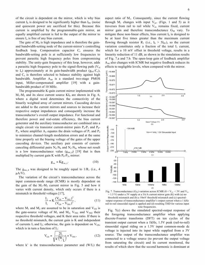
aspect ratio of M1. Consequently, since the current flowing through M1 changes with input Vin+ (Figs. 1 and 5) as it traverses from rail to rail while Vin- remains fixed, current mirror gain and therefore transconductance GM vary. To mitigate these non-linear effects, bias current Ib is designed to be at least five times greater than the maximum current flowing through resistor R1 (i.e., Ib > 5IR1), so the current variation constitutes only a fraction of the total I1 current, which for a 10 mV offset in threshold voltage, results in a linearity reduction of 11 dB, as shown in the simulation results of Fig. 7.a and 7.b. The open-loop gain of feedback amplifier Aint also changes with ICMR but negative feedback reduces its effects to negligible levels, when compared with the mirror.
-90
-110
-130
-150
-170
-190
-210
-2300.0 2 kHz 4 kHz
-104.4dB
-216.1dB
Out
put C
urre
nt M
agni
tude
(dB
)
(c)
-140
-120
-100
-80
-60
-40
-20
0
1kHz 10kHz 100kHz 1MHz 10MHz
THD(dB)
(d)
Vin+=1 kHz, 1.5V Sinusoidal Input
1 kHz 3 kHz 5 kHz 6 kHz
3.02.01.00-19.597-19.595-19.593-19.591-19.589-19.587-19.585-19.583
-19.873
-19.872
-19.871
-19.870
-19.869
-19.868
Input Voltage (V)
Tran
scon
duct
ance
(µA
/V)
Tran
scon
duct
ance
(µA
/V) (a) 3.02.01.00
(b)
Fig. 7. Transconductance (GM) variation across ICMR (0 < Vin+ < 3V and Vin-
= 1.5 V) under a 3V supply at a 5A/A current mirror gain (K) with (a) no threshold mismatch and (b) a 10mV threshold mismatch and (c) spectral-
output response of transconductance amplifier’s output current when a 1 kHz rail-to-rail sinusoidal signal is applied and (d) resulting THD for various input
tone frequencies. Fig. 7(c) shows the simulated spectral-output response of
the foregoing transconductance amplifier when applying discrete-Fourier transforms (DFT) on ten cycles of the transient output current when a 1kHz, 1.5V peak (rail-to-rail) sinusoidal signal riding on a 1.5V input common-mode dc voltage is injected into its input while supplied from a 3V source. The output of the transconductance amplifier was connected to a voltage source (to prevent the output voltage from saturating the circuit) and its current monitored, the results of which show that the second harmonic is dominant at

7
110dB below the fundamental, as expected, given the asymmetrical nature of the circuit topology. The experiment was repeated for different input tones and Fig. 7(d) shows the total harmonic distortion (THD) results for various input frequencies. The circuit is highly linear at low frequencies because the loop gain in the feedback loop comprised of amplifier Aint, transistor M3, and resistor R1 is high. As frequency increases and loop gain decreases, however, the linearity decreases and THD increases from approximately -115dB at 1kHz to -40dB at 10MHz.
B. Tunable Resistor R The bandwidth of the GM-C filter is tuned by adjusting its
shunting load resistance (R in Fig. 1). A 1 kΩ/□ binarily weighted polysilicon resistor is used for this (Fig. 8). Resistor R1 from Fig. 5 is not tuned because the parasitic capacitors introduced by the switches limit the overall frequency response of the filter. These parasitic capacitors, on the other hand, have negligible effects when applied to R in Fig. 1 because bandwidth-setting capacitor C is in parallel with R and it is already relatively large.
Ru 4Ru 2Ru Ru Ru/2 Ru/4 Ru/8 Ru/16 Ru/32t1 t2
d1d2d3d4d5d6 d0d7
Fig. 8. Programmable and binarily weighted polysilicon resistor R.
Programmability is achieved by decoding a digital word and deciphering the connectivity of controlling NMOS switches d7-d0 from it. When bits d7-d0 are all one, all the switches are closed, short-circuiting the large resistor and resulting in an overall resistance of Ru, the minimum resistance value. As the bit word d7-d0 progresses from all ones to all zeros, the switch resistance increases to 9Ru in Ru/32 increments. The aspect ratios of the transistors are sufficiently large to prevent their respective switch-on resistances from degrading the resolution of the resistor array (i.e., Rd0 is significantly lower than Ru/32), which in this case is 3.2% of Ru/32. Only NMOS devices were used because the supply voltage in the foregoing application was high enough (> 3 V) above the switch terminal voltages (0.7 – 1.35 V) during worst-case conditions to guarantee sufficient gate-drive to short-circuit any resistor in the array. Had the supply voltage been lower or the terminal voltages higher, a PMOS switch would have been placed in parallel with each NMOS device.
C. Non-Overlapping Clocks Dead time between two clock signals can be inserted by
first having each signal sense the other and only allowing a pulse to propagate when the other is off and second by inserting a delay. The NOR gates of the non-overlapping clock generator circuit shown in Fig. 9 perform the sensing and gating function whereas the resistance of weak inverter I0p1x in combination with capacitors Cd1 and Cd2 insert a delay of approximately 100 ns between non-overlapping clocks φ and φn. The output signals were designed to have rise and fall times of roughly 10 ns.
Pulse_In
φCd1
Cd2
I0p1x
I0p1x I1x
I1x I10x I10x
I10x I10x φn
Fig. 9. Non-overlapping clock generator circuit.
The “Pulse_In” is a 1 kHz, 50% duty cycle digital clock signal derived from a single-phase system clock (e.g., ring oscillator). Offset cancellation performance degrades at clock frequencies below 10 Hz because the storage capacitors are discharged by leakage currents and above 10 kHz because the amplifier is not fast enough to settle to its ideal steady-state value during the offset-programming phase [3]. Clock frequency uncertainties resulting from jitter are minimal at low frequencies (e.g., 1 kHz), and even if jitter were present, offset would still be unaffected because at 1 kHz more than enough settling time (i.e., margin) exists for the offset programming phase to settle. The entire system was simulated and verified over the voltage lifespan of a Li-Ion battery (3 – 4.2 V), a military temperature range of -40 to 125 °C, and process corner variations (i.e., slow and fast MOS transistor models and ±20% capacitor, resistor, and bias current variations). Monte Carlo mismatch analysis was also performed to study the offset and linearity performance of the system.
V. EXPERIMENTAL RESULTS The proposed circuit was designed and fabricated with
AMI’s 0.5-µm CMOS process technology. The GM-C filter die photograph is illustrated in Fig. 10 and its top-level design parameters are summarized in Table 3. Transconductance-setting resistor R1 is 250 kΩ, bandwidth-setting capacitor C is 60 pF, mirror-gain range is 1-5 with seven bits of resolution, bandwidth-setting resistor range is 325 to 2,900 kΩ with eight bits of resolution, and the auto-zeroing clock frequency is 1 kHz. The DC gain and bandwidth of the filter were adjustable from 1.27 to 29.16 V/V and 1.1 to 6.4 kHz, respectively, partial experimental results of which are shown in Fig. 11.
To minimize clock feed-through and charge-injection errors, hold capacitor pairs Ch1+-Ch1- and Ch2+-Ch2- should match and were therefore placed close to each other and laid out using cross-coupling and common-centroid techniques. Similarly, to reduce initial offsets in the transconductor, the same techniques were applied to the transistors used in the current mirror and current source. Transconductance cells GM1 and GM2 were also placed next to each other and oriented in the same direction for the same reason. For tuning linearity, tuning resistor segments were interdigitated and their periphery surrounded with dummy resistors to reduce etch-induced mismatch effects.
8
Fig. 10. Die photograph of the 0.5-µm CMOS GM-C filter (870 µm x 890
µm).
Table 3. Important GM-C Filter Design Parameters.
Parameter Value Transconductance-Setting Resistor (R1) 250 kΩ
GM Range (GM-min - GM-max) 4 – 20 µA/V Minimum Programming Resolution of GM
(∆GM / GM-min) 3.125%
R Range (Rmin - Rmax) 325 - 2,900 kΩ Minimum Programming Resolution of R
(∆R / Rmin) 3.125%
Bandwidth-Setting Capacitor (C) 60 pF Hold Capacitors (Ch11, Ch12, Ch21, and Ch22) 6 pF
Auto-Zeroing Clock Frequency 1 kHz
The GM-C filter was subjected to the low impedance rail-to-rail signal generated by a current-mode switching buck regulator circuit (as shown in Fig. 1) and used to sense and control the regulator’s current-mode feedback. The experimental transient results are illustrated in Fig. 12, and as expected, the square wave is integrated into a triangle by the GM-C filter. The ping-pong “handover” event referred to in the transient glitch analysis section of this paper is highlighted in Fig. 12(b) and shown to be less than 40 mV for worst-case DC output voltage conditions (i.e., largest Vo-to-Vref voltage difference). Although the resulting transient glitch effectively changes the duty cycle of the converter (because its output is used, in part, to control the switching supply), its net effect is negligible and easily compensated within one switching cycle.
-20
-10
0
10
20
30
0.1 1 10 100Frequency (kHz)
Gai
n (d
B)
=Min, R=Max =2*Min, R=Min =Min, R=Min
BW=1.1 kHz
BW=6.4 kHz
BW=6.4 kHz
gm
gm
gm
Fig. 11. Experimental frequency response of GM-C filter.
To verify the offset cancellation capability of the circuit, one of the transconductors was disabled and the other observed, short-circuiting the input and monitoring the output of the transconductor before (Vo1 in Figs. 2 and 3) and after it is connected to bandwidth-setting capacitor C (Vo) via on-chip buffers, as shown in Fig. 13. The peak-to-peak voltage of Vo represents the cumulative output-referred offset voltage of the summing transconductor because Vo is clamped to Vref when disconnected from the transconductor and auto-zeroed to Vref – (VosgmR) when connected. The resolution of the oscilloscope was unfortunately limited to approximately 5 mV, limiting the measurement’s input-referred offset resolution to approximately 500 µV (5 mV / 9.92 V/V).
Input Voltage (In+)
Vo
(a)
(b)
Transient Vo
ϕ clock
Fig. 12. (a) The GM-C filter’s response to a rail-to-rail square wave and (b) the
zoomed-in effects of the ping-pong “handover” transition on the response.

9
To improve the accuracy of the measurement, the output of
the GM-C filter and therefore the offset of the same were amplified on-chip by 26 dB before measuring it with the oscilloscope, as shown in Fig. 14. Consequently, when GM-C output Vo is disconnected and clamped to Vref, both inputs of the amplifier in the gain stage are at Vref and the output is therefore zero. However, when the auto-zeroed transconductor is connected, the output voltage difference to Vref is amplified and measured. The clocking sequence of the test setup was as follows: (1) GM-C filter inputs are short-circuited on-chip and transconductor 1 is auto-zeroed, (2) auto-zero is disabled and transconductor 1 is connected to bandwidth-setting capacitor C with GM-C filter inputs still short-circuited on-chip, and (3) GM-C filter inputs are disconnected on-chip but reconnected off-chip.
VDD=3.3V, Gain=11.7
Vo
Vo1
ϕ
Vin=0, VDD=3.2V, VICM=1.2V, gmR=9.92
Fig. 13. Ping-ponging between the auto-zeroed transconductor and Vref.
Vid
Vobuf
Vref
SW1
Ch2
Ch2 R
GMϕn
SW2
-
+
190K10K
ϕϕVpreamp
1
1
SW1
SW2
ϕ
ϕnVref
Auto Zero Gain
Vo-+
+-
C
Vref
a
Fig. 14. A 26 dB gain stage is added to increase the measurement resolution of
the offset.
Since the circuit is designed to filter the voltage across an
off-chip inductor, the voltage difference between the first and third phases of the clocking sequence is the output-referred offset voltage of the transconductor. Because the offset of the additional gain stage is common-mode to all phases and only the differential voltage between phases is measured, the preamplifier’s input-referred offset has no effect on the accuracy of the measurements. The amplified output-referred offset under various conditions (power supply of 3 and 4.2 V and input common-mode range of 1, 1.2, and 1.5 V) are shown in Fig. 15. The resulting input-referred offset for three samples was less than ± 210 µV (42 mV divided by the GM-C filter’s gain of 9.92 and pre-amplifier gain of 20). A slight dependence to supply voltage was observed, as anticipated in Eq. 3, for which high PSRR design techniques can be used.
The 40 µV difference between phase 2 and phase 3 input voltages (8 mV divided by the GM-C filter’s gain of 9.92 and pre-amplifier gain of 20) occurs because the off-chip short-
SW1
VDD=4.2 V, VICM=1.2 V, gmR=9.92, R=max, Vid=0
( ) os_eq_inm VRg20 ××
SW1
VDD=3 V, VICM=1 V, gmR=9.92, R=max, Vid=0
(a)
(b)
SW1
oV20×
VDD=3 V, VICM=1.2 V, gmR=9.92, R=max, Vid=0
(c)
(d)
SW1
oV20×
VDD=3 V, VICM=1.5 V, gmR=9.92, R=max, Vid=0
oV20× oV20×
( ) os_eq_inm VRg20 ××
( ) os_eq_inm VRg20 ××( ) os_eq_inm VRg20 ××
Phase 1Phase 2
Phase 3
Phase 1
Phase 1Phase 2
Phase 3
Phase 1Phase 2
Phase 3Phase 1
Phase 2Phase 3
Fig. 15. Offset measurements under various supply and common-mode input voltage conditions.

10
circuit condition is not ideal. Issues such as thermocouple effects can cause non-zero input voltages at the input of the transconductor during the offset measurement phase.
The circuit was operational for auto-zeroing clock frequencies ranging from 10 Hz to 10 kHz. At higher frequencies, as alluded to earlier, the auto-zeroing properties were diminished because the circuit does not have enough time to settle to its auto-zeroed value. On the other extreme, the hold capacitors limit the amount of time the auto-zeroed voltage is held in the presence of leakage currents from parasitic reverse-biased junction diodes, which is worst at high temperatures where leakage currents are at their highest levels [3, 20]. Since DC offsets are nothing more than low frequency signals, dynamic offset-cancellation schemes also reduce 1/f low frequency noise. Given the low bandwidth nature of the GM-C filter, output noise is further reduced, and in the foregoing case, the total input-referred noise was measured to be 93 µV with a filter DC gain of about ten at RMax. The circuit’s nonlinearity performance (ΔGM/GM) was found to be -57 dB by measuring the resulting common-mode input-induced systematic offset for a rail-to-rail non-inverting input signal. Table 4 summarizes these and the other experimental performance parameters of the circuit.
Table 4. Measured Performance of the Proposed CMOS GM-C Filter.
Technology AMI’s 0.5-µm CMOS Chip Area 870 µm x 890 µm Supply Voltage 3 - 4.2 V Supply Current
Min GM1 Max GM1
0.62 mA 1.20 mA
BW (1/RC) Programmability (resolution for worst case – min. R)
1.1 - 6.4 kHz (3.2% resolution)
Gain (GM1R) Programmability (resolution for worst case – min. GM1)
1.27 - 29.16 V/V (3.2 % resolution)
Input-Referred Offset (Gain = 9.92, max. R, 3 units tested) < ± 210 µV
Power-Supply Rejection Ratio (DC) 74 dB Common-Mode Rejection Ratio (DC) 83 dB In- ICMR (V) 0.5 V to (VDD - 1) In+ ICMR (V) -0.4 V to VDD Transconductance Non-Linearity (ΔGM/GM) Rail-to-Rail Vin+, VDD = 3 V, Vin- = 1.5 V
-57 dB
Total Input-Referred Noise (C = 60 pF, Gain = 9.92, max. R) 93 µV
Second Pole 4 MHz Ping-Pong (“Handover”) Transient Glitches < 40 mV
VI. CONCLUSIONS A programmable and linear low offset 0.5-µm CMOS GM-C
filter has been proposed, designed, fabricated, and evaluated. The experimental offset was measured to be less than ± 210 µV for 3 to 4.2 V supply voltages (lithium-ion battery supply range) and 1 to 1.5 V input common-mode voltages. The DC gain and bandwidth were adjustable from 1.1 to 6.4 kHz and 1.27 to 29.16 V/V, respectively, both with better than 3.2% resolution by adjusting the transconductance via the gain of a
current mirror and the resistance of a shunting bandwidth-setting resistor. “Handover” glitches during ping-pong transitions were less than 40 mV while achieving a nonlinearity performance of -57 dB. The low input-referred offset, high linearity, continuity, and programmable features achieved with this design are appealing to a growing number of high performance analog systems, from power-hopped switching power supplies to front-end interface electronics for telemetry applications, and all under the constraints of CMOS integration. Analog filters, however, which are prevalent in most, if not all, applications that interface with the real world, benefit the most from these performance characteristics.
ACKNOWLEDGMENT The authors would like to thank MOSIS for fabricating the
IC prototype chip, Huseyin Dinc and Vishal Gupta from Georgia Tech, John Seitters from Intersil, and the Reviewers for their valuable comments and suggestions.
REFERENCES [1] M. Pertijs, K. Makinwa, and J. Huijsing, “A CMOS smart temperature
sensor with a 3-σ inaccuracy of ±0.1 oC from -55 oC to 125 oC,” IEEE Journal of Solid-State Circuits, vol. 40, pp. 2805-2815, Dec. 2005.
[2] M. Tavakoli and R. Sarpeshkar, “An offset-canceling low-noise lock-in architecture for capacitive sensing,” IEEE Journal of Solid-State Circuits, vol. 38, pp. 244-253, Feb. 2003.
[3] C. Enz and G. Temes, “Circuit technique for reducing the effects of circuit imperfections,” Proceedings of IEEE, 1586-1614, Nov. 1996.
[4] A. Bakker, K. Thiele, and J. H. Huijsing, “A CMOS nested-chopper instrumentation amplifier with 100-nV offset,” IEEE Journal of Solid-State Circuits, vol. 35, pp. 1877-1883, Dec. 2000.
[5] C. Enz, E. Vittoz, and F. Krummenacher, “A CMOS chopper amplifier,” IEEE Journal of Solid-State Circuits, vol. SC-22, pp. 335-342, June 1987.
[6] C. Yu and R. Geiger, “Precision offset compensated op-amp with ping-pong control,” GOMAC-92 Dig., pp. 189-190, 1992.
[7] Y. Chong-Gun and R. Geiger, “An Automatic offset compensation scheme with ping-pong control for CMOS operational amplifiers,” IEEE Journal of Solid-State Circuits., pp. 601-610, May 1994.
[8] I. Opris and G. Kovacs, “A rail-to-rail ping-pong op-amp,” IEEE Journal Solid-State Circuits, pp. 1320-1324, Sept. 1996.
[9] M. Coln, “Chopper stabilization of MOS operational amplifiers using feed-forward techniques,” IEEE Journal of Solid-State Circuits, vol. 16, pp. 745-748, Dec. 1981.
[10] I. Finvers, J. Haslett, and F. Trofimenkoff, “A high temperature precision amplifier,” IEEE Journal of Solid-State Circuits, vol. 30, pp. 120-128, Feb. 1995.
[11] H.P. Forghani-zadeh and G.A. Rincón-Mora, “A Lossless, Accurate, Self-Calibrating Current-Sensing Technique for DC-DC Converters,” in Proc. 2005 Industrial Electronics Conference (IECON), pp. 549 - 554.
[12] E. Dallago, M. Passoni and G. Sassone, “Lossless current sensing in low voltage high current DC/DC modular supplies,” IEEE Trans. Industrial Electronics, vol. 47, pp. 1249-1252, Dec. 2000.
[13] H.P. Forghani-zadeh and G.A. Rincón-Mora, “A continuous, low-glitch, low-offset, programmable gain and bandwidth gm-C filter,” in Proc. 2005 Midwest Symposium on Circuits and Systems (MWSCAS), pp. 1629 - 1632.
[14] ICL7650S, 2MHz, Super Chopper-Stabilized Operational Amplifier, Milpitas, CA: Intersil Corporation, http://www.intersil.com, Aug 2005.
[15] MAX420, ±15V chopper-stabilized operational amplifier, Milpitas, CA, Maxim Integrated Products Inc., http://www.maxim-ic.com, Aug 2005.
[16] C. Toumazou, J. Lidgey, and D. Haigh, Analogue IC design: the current-mode approach, Peter Peregrinus Ltd: London, UK, 1990.
[17] K. Koli, CMOS Current Amplifiers: Speed versus Nonlinearity, Ph.D. Dissertation, Helsinki University of Technology, 2000.
[18] H. Elwan, A. Soliman, “Low-voltage low-power CMOS current conveyors,” IEEE Transactions on Circuits and Systems-I, vol. 44, pp. 828-835, Sept. 1997.

11
[19] P. Allen and D. Holberg, CMOS Analog Circuit Design, Oxford, NY: Oxford university press, 2002.
[20] D. Johns and K. Martin, Analog Integrated Circuit Design. New York, NY: Wiley, 1997.
H. Pooya Forghani-Zadeh received the B.S. degree in electrical engineering from Sharif University of Technology, Tehran, Iran, in 2000 and the M.S. and Ph.D. degrees from Georgia Institute of Technology, Atlanta, GA, in 2003 and 2006, respectively. He has been with the Custom Mixed Signal group of Texas Instruments Incorporated, Dallas, TX, as an Analog Circuit Designer since November 2005.
Gabriel A. Rincón-Mora (S’91–M’97–SM’01) received the B.S.E.E. degree from Florida International University (High Honors) in 1992 and the M.S.E.E. and Ph.D. degrees from Georgia Tech (Outstanding Ph.D. Graduate) in 1994 and 1996, respectively. He worked for Texas Instruments Inc. defining and designing integrated power management circuit solutions for cellular phones, pagers, laptop and desktop computers, and others from 1994 to 2003 as Senior Integrated Circuits Designer, Design Team Leader, and Member of Group Technical Staff, and from 2003 to 2005 as Senior Analog Consultant. In 1999, he was appointed Adjunct Professor for Georgia Tech and in 2001 he became a full-time faculty member of its School of Electrical and Computer Engineering. From 2002 to 2004, he was the Director of the Georgia Tech Analog Consortium. In April of 2005, he founded and is now the administrator of the Analog Undergraduate Outreach Program. His research is on designing and developing power efficient, high performance, totally integrated, system-on-chip (SoC) and system-in-package (SiP) power management solutions for mobile applications (e.g., energy harvesting, micro-scale fuel cells, thin-film lithium-ion batteries, inductor multipliers, etc.). His scholarly products include 4 books as sole author, 25 patents, 98 publications, and 26 commercial power management chip designs. Dr. Rincón-Mora received the National Hispanic in Technology Award from the Society of Professional Hispanic Engineers, the Charles E. Perry Visionary Award from Florida International University, a Commendation Certificate from the Lieutenant Governor of California, and Orgullo Hispano and Hispanic Heritage awards from Robins Air Force Base. He was inducted into the Council of Outstanding Young Engineering Alumni by Georgia Tech and featured on the cover of Hispanic Business Magazine as one of The 100 Most Influential Hispanics, La Fuente (Dallas Morning News publication), and three times on Nuevo Impacto (Atlanta-based magazine). He is the Technical Program Co-Chair for IEEE’s 2007 Joint Midwest Symposium of Circuits and Systems (MWSCAS) and NEWCAS in Montreal, Technical Program Co-Chair for IEEE’s 2006 Midwest Symposium of Circuits and Systems (MWSCAS) in Puerto Rico, Chairman of Atlanta’s joint IEEE Solid-State Circuits and Circuits and Systems Society (SSCS-CASS) since 2005, Vice Chairman of Atlanta’s SSCS-CASS in 2004, Steering Committee Member for IEEE’s Midwest Symposium on Circuits and Systems since 2006, Selection Committee Review Panelist for the National Science Foundation since 2003, and member of IEEE’s Circuits and Systems’ Analog Signal Processing Technical Committee since 2003. He is a life member of the Society of Hispanic Professional Engineers (SHPE), and a member of IEE. He is also a member of Eta Kappa Nu, Phi Kappa Phi, and a life member of Tau Beta Pi.


![D}µv ]v Z]o v[ &}µv ]}v - Mountain Children's Foundationmcfglobal.ngo/wp-content/uploads/2019/08/MCF-Annual...D}µv ]v Z]o v[ &}µv ]}v Annual Report 2018-2019 Change a child: change](https://img.pdfslide.net/doc/110x75/5f16385fa0c7856d2c0915b7/dv-v-zo-v-v-v-mountain-childrens-dv-v-zo-v-v.jpg)


![60 NJU7056/NJU7057/NJU7058 V] 1 Rail-to-Rail … Low Noise, Low Offset Voltage Drift Rail-to-Rail Output CMOS Operational Amplifier FEATURES(V+=5V, V-=0V, Ta=25 C) GENERA](https://img.pdfslide.net/doc/110x75/5ae3c5997f8b9a595d8edf03/60-nju7056nju7057nju7058-v-1-rail-to-rail-low-noise-low-offset-voltage-drift.jpg)


![:µv]}îìíð Z yvµo o ]. ] v](https://img.pdfslide.net/doc/110x75/62d66fb405939762596e03c9/v-z-yvo-o-v.jpg)
