Embed Size (px)
Citation preview
Politecnico di Milano
Dipartimento di Elettronica e Informazione
Dottorato di Ricerca in Ingegneria dell'Informazione
A Reliability-aware
Design Methodology
for Embedded Systems
on Multi-FPGA Platforms
Doctoral Dissertation of:
Chiara Sandionigi
738757
Advisor:Prof. Cristiana Bolchini
Tutor:Prof. Donatella Sciuto
Supervisor of the Doctoral Program:Prof. Carlo Ettore Fiorini
2011 � XXIV

Politecnico di Milano
Dipartimento di Elettronica e InformazionePiazza Leonardo da Vinci, 32 I-20133 � Milano


A mia mamma

Ringraziamenti
Tre anni di dottorato sembrano ora essere passati molto velocemente,forse troppo velocemente. Qualche tempo fa stavo discutendo una tesiche segnava la �ne del mio periodo da studentessa di ingegneria, e oraho appena concluso una nuova tesi che segnerá la �ne di questa intensae bellissima esperienza al Politecnico. Tra questi due momenti, che a mesembrano essere cosí vicini tra loro, c'é stata una vita vissuta a Milano,c'é stato un anno trascorso in Olanda tra la vita a Leiden e il lavoro inESA, ci sono stati i viaggi, le conferenze, le riunioni e gli eventi dellaPhDEI association, e cosí tante esperienze da non poter riassumere inqueste poche righe. É stato un percorso professionale e personale che nonavrei potuto compiere senza il sostegno di alcune persone, a cui vanno imiei ringraziamenti.La prima persona che ringrazio é Cristiana, relatrice di questa tesi.
Noi non ci siamo propriamente scelte per questo percorso di dottorato,ma credo che di�cilmente avrei potuto avere advisor migliore. Lei ésempre stata presente, anche quando ero in Olanda, dandomi consigli eindicazioni su come portare avanti il mio lavoro. Questa tesi non sarebbestata possibile senza il suo aiuto.Un grazie per i preziosi consigli va anche ad Antonio. Forse a volte con
altri ha risposto con aria di su�cienza (scusa Antonio, ma non potevonon scriverlo :) ), ma con me Antonio é sempre stato molto disponibile ela sua esperienza mi é stata di enorme aiuto. Inoltre lui é stato parte di unu�cio che mi dispiacerá veramente molto lasciare, insieme a Christian,Daniele, Luigi, Marco e PRG.Un ringraziamento va poi ad ESA, e in particolare alla Sezione di Mi-
croelettronica, senza il cui supporto questo dottorato non sarebbe statopossibile. Grazie per avermi dato la possibilitá di lavorare un anno in ES-TEC, e in generale di vivere un anno in Olanda, e grazie per il sostegno,in particolare grazie a Luca e a David per il loro aiuto. Allo stesso modoringrazio Donatella e Marco, senza i quali questa esperienza per me nonsarebbe neanche iniziata. Il dottorato per me é stato un'esperienza im-portante, una scelta che rifarei senza esitazioni, quindi grazie in�nite peravermi dato questa opportunitá.Al Politecnico ho potuto conoscere e lavorare con persone che spero
faranno sempre in qualche modo parte della mia vita, dovunque andró
V
in futuro. Tra queste persone c'é Danilo, mio relatore di minore e amico.Lavorare con lui é stato istruttivo e divertente allo stesso tempo, e sperotanto di poter ripetere questa esperienza in futuro.In�ne, parlando del Politecnico, non posso dimenticare la PhDEI as-
sociation, e in particolare la mia �mamma mora� e la mia �mamma lam-pone�, Annalisa e Rossella. Grazie per i sorrisi e grazie perché so che cisaranno sempre nonostante la lontananza.Ed eccomi ora arrivata alla vita al di fuori delle mura del Poli e ai
ringraziamenti per i miei migliori amici. Un grazie di cuore va a Stefania,mia migliore amica, che mi é accanto sempre e comunque. Spero che leisappia quanto é importante per me e quanto io apprezzi tutto ció che fa.Un grazie va poi a Michele, sempre pronto ad ascoltare (e a tollerare chegli invada casa a qualsiasi ora :) ). E un grazie va a Fabrizio, che é inqualche modo entrato nella mia vita solo di recente, ma mi ha ascoltato esupportato (o sopportato) molto durante questi ultimi mesi di dottorato.Un grazie di cuore é poi naturalmente per Alessio, mio migliore amico
e ormai da tempo con�dente. So che per noi lontananza vuol dire soloavere piú cose da raccontarci quando ci rivedremo.In�ne, �last but not least�, un ringraziamento va alla mia famiglia e
in particolare alla persona a cui é dedicata questa tesi, mia mamma, cheda sempre mi supporta qualunque siano le mie scelte.Grazie a tutti per questi tre importanti e intensi anni che hanno por-
tato a questa tesi.
VI
Abstract
In the last decades, Static RAM (SRAM) Field Programmable Gate Ar-rays (FPGAs) have become an attractive technology for the electronicsof embedded systems, for both fast prototyping and �nal production.Their most attractive feature is the �exibility, related to the opportunityof re-programming (or recon�guring) the device in a few clock cyclesand on-line, while the device is operating. This allows the system imple-mented on the FPGA to be updated/upgraded, also remotely.SRAM-based FPGAs are currently employed in many applicative do-
mains and their use is being investigated also for mission-critical appli-cations, such as the space scenario, the reference settings for this thesis.In fact, in the space environment, such devices are an attractive tech-nology for the possibility of remote update/upgrade, coping with thedi�culty of system maintenance. Nevertheless, the harsh environmentalconditions and the long lifetime required for space systems prevent thestraightforward adoption of SRAM-based FPGAs, due to their suscepti-bility to faults. In fact, this same environment is particularly critical forstatic RAM technology, susceptible to physical phenomena that causeboth transient and permanent faults. Thus, appropriate tolerance andrecovery techniques are adopted; in general, fault tolerance techniquesare mostly based on spatial redundancy, whereas recovery ones exploitthe FPGAs' recon�guration capability, allowing to cope with the occur-rence of faults by re-programming the faulty parts.Indeed, hardened systems may require many resources due to their size
and complexity, hence a single device may not su�ce in terms of availableresources, and multi-FPGA solutions are taken into account and inves-tigated. Furthermore, the availability of more devices on multi-FPGAplatforms can be exploited to increase reliability as the overall func-tionality is spread over multiple devices, possibly also using redundantimplementations.The research proposed in this PhD thesis �ts in the described scenario.
The aim is the de�nition of a reliability-aware methodology for the designof embedded systems on multi-FPGA platforms. The designed systemmust be able to detect faults occurrence globally and autonomously, inorder to recover or to mitigate the e�ects of the faults. Two categoriesof faults are identi�ed, based on their impact on the device elements;
VII

i) non-recoverable faults, that are those that cause a permanent problem,making the portion of the fabric unusable, and ii) recoverable faults,transient problems that can be �xed without causing a lasting e�ect.While some aspects can be taken from previous solutions available
in literature, several open issues exist. In fact, reliability techniqueshave been widely addressed in the case of systems based on a singleFPGA, but the problem extended to multi-FPGA platforms has beenrarely taken into account. Indeed, the single FPGA approaches can notbe straightforwardly adopted for the multi-FPGA scenario, that posesseveral challenges, as, for instance, the partitioning of the system amongthe available devices. Furthermore, in the previous contributions, onlyrecoverable faults are usually targeted, whereas non-recoverable ones arerarely analyzed. Thus, no complete design methodology handling all thepeculiar issues of the considered scenario has been proposed yet, a gapwe aim at �lling with our work.Not only we de�ne the methodology in its relevant aspects, but we
also design and develop a framework for supporting the designer in itsapplication. The �nal system thus exposes reliability properties andincreases its overall lifetime and availability.
VIII
Riassunto
Negli ultimi decenni, i dispositivi FPGA (Field Programmable Gate Ar-ray) basati su SRAM (Static RAM) sono diventati una tecnologia diinteresse per l'elettronica dei sistemi dedicati, sia per la prototipazioneveloce che per la produzione �nale. La loro caratteristica di maggio-re interesse é la �essibilitá, relativa all'opportunitá di riprogrammare(o ricon�gurare) il dispositivo in pochi cicli di clock e on-line, mentreil dispositivo é operativo. Questo permette di aggiornare/migliorare ilsistema implementato sulla FPGA, anche remotamente.Le FPGA basate su SRAM sono attualmente impiegate in molti domi-
ni applicativi e il loro uso viene vagliato anche per applicazioni critiche,come lo scenario delle missioni spaziali, di riferimento per questa tesi.Infatti, nell'ambiente spazio, tali dispositivi sono una tecnologia di in-teresse per la possibilitá di aggiornamento/miglioramento remoto, chefa fronte alla di�coltá di manutenzione del sistema. Tuttavia, le di�-cili condizioni ambientali e il lungo tempo di vita richiesto per i sistemiper lo spazio ostacolano l'immediata adozione delle FPGA basate suSRAM, a causa della loro sensibilitá ai guasti. Infatti, questo stesso am-biente é particolarmente critico per la tecnologia RAM statica, sensibilea fenomeni �sici che causano guasti sia transitori che permanenti. Diconseguenza, vengono adottate appropriate tecnologie di tolleranza e re-cupero; in generale, le tecniche di tolleranza sono per lo piú basate sullaridondanza spaziale, mentre quelle di recupero sfruttano la capacitá diricon�gurazione delle FPGA, permettendo di far fronte al veri�carsi deiguasti riprogrammando le parti guaste.Invero, i sistemi irrobustiti possono richiedere molte risorse a causa del-
la loro dimensione e complessitá, quindi un singolo dispositivo puó nonessere su�ciente in termini di risorse disponibili, e le soluzioni multi-FPGA vengono prese in considerazione e valutate. Inoltre, la disponibi-litá di piú dispositivi sulle piattaforme multi-FPGA puó essere sfruttataper aumentare l'a�dabilitá poiché la funzionalitá globale é distribuita supiú dispositivi, eventualmente anche usando implementazioni ridondanti.La ricerca proposta in questa tesi di dottorato si inserisce nello scenario
descritto. L'obiettivo é la de�nizione di una metodologia orientata all'af-�dabilitá per il progetto di sistemi dedicati su piattaforme multi-FPGA.Il sistema progettato deve essere in grado di identi�care il veri�carsi di
IX

guasti globalmente e autonomamente, per recuperare o mitigare gli ef-fetti dei guasti. Vengono identi�cate due categorie di guasti, in base alloro impatto sugli elementi del dispositivo: i) guasti non recuperabili, chesono quelli che causano un problema permanente, rendendo inutilizzabilela porzione del dispositivo, e ii) guasti recuperabili, problemi transitoriche possono essere risolti senza causare un e�etto persistente.Nonostante alcuni aspetti possano essere presi da soluzioni precedenti
disponibili in letteratura, esistono molti punti aperti. Infatti, le tecni-che di a�dabilitá sono state ampiamente a�rontate nel caso di sistemibasate su una singola FPGA, ma il problema esteso alle piattaformemulti-FPGA é stato raramente preso in considerazione. Invero, gli ap-procci per singola FPGA non possono essere direttamente adottati perlo scenario multi-FPGA, che pone molte s�de, come, per esempio, il par-tizionamento del sistema tra i dispositivi disponibili. Inoltre, nei contri-buti precedenti, sono di solito trattati solo i guasti recuperabili, mentrequelli non recuperabili sono raramente analizzati. Di conseguenza, noné ancora stata proposta una metodologia di progetto completa che ge-stisca tutti i problemi peculiari dello scenario considerato, un vuoto chepuntiamo a colmare con il nostro lavoro.Non solo de�niamo la metodologia nei suoi aspetti rilevanti, ma inoltre
progettiamo e sviluppiamo una struttura che supporti il progettista nellasua applicazione. Di conseguenza il sistema �nale espone proprietá dia�dabilitá e aumenta il suo tempo di vita globale e la sua disponibilitá.
X
Contents
1. Introduction 1
1.1. Research overview and statement of originality . . . . . . 21.2. Publications . . . . . . . . . . . . . . . . . . . . . . . . . . 4
2. Motivations and working scenario 7
2.1. Motivations . . . . . . . . . . . . . . . . . . . . . . . . . . 72.2. Fault model . . . . . . . . . . . . . . . . . . . . . . . . . . 92.3. Working scenario: the space environment . . . . . . . . . 10
2.3.1. Radiation e�ects . . . . . . . . . . . . . . . . . . . 112.3.2. Aging e�ects . . . . . . . . . . . . . . . . . . . . . 122.3.3. Adopted fault classi�cation . . . . . . . . . . . . . 12
2.4. Chapter summary . . . . . . . . . . . . . . . . . . . . . . 13
3. Proposed reliability-aware design methodology 15
3.1. Reliability-aware design methodology . . . . . . . . . . . . 153.2. Proposed autonomous fault tolerant system . . . . . . . . 173.3. Additional fault scenarios . . . . . . . . . . . . . . . . . . 203.4. Chapter summary . . . . . . . . . . . . . . . . . . . . . . 21
4. Design �ow and framework 23
4.1. Design �ow . . . . . . . . . . . . . . . . . . . . . . . . . . 234.2. Multi-FPGA platform model . . . . . . . . . . . . . . . . 254.3. Preliminary partitioning . . . . . . . . . . . . . . . . . . . 274.4. Circuit hardening . . . . . . . . . . . . . . . . . . . . . . . 30
4.4.1. Recovery strategy de�nition . . . . . . . . . . . . . 314.4.2. Independently recoverable areas de�nition . . . . . 34
4.5. Validation . . . . . . . . . . . . . . . . . . . . . . . . . . . 374.5.1. Recovery strategy re�nement . . . . . . . . . . . . 374.5.2. Reliability-aware partitioning . . . . . . . . . . . . 38
4.6. Floorplanning . . . . . . . . . . . . . . . . . . . . . . . . . 424.7. Prototype framework . . . . . . . . . . . . . . . . . . . . . 444.8. Design �ow for �xed number of non-recoverable faults . . 454.9. Chapter summary . . . . . . . . . . . . . . . . . . . . . . 46
XI
Contents
5. Fault classi�cation 49
5.1. Related work . . . . . . . . . . . . . . . . . . . . . . . . . 495.2. First preliminary proposal . . . . . . . . . . . . . . . . . . 505.3. Second preliminary proposal . . . . . . . . . . . . . . . . . 52
5.3.1. Fault quanti�cation . . . . . . . . . . . . . . . . . 525.3.2. Proposed classi�cation algorithm . . . . . . . . . . 545.3.3. Algorithm evaluation . . . . . . . . . . . . . . . . . 56
5.4. Fault Classi�er speci�cation . . . . . . . . . . . . . . . . . 585.5. Algorithm evaluation . . . . . . . . . . . . . . . . . . . . . 61
5.5.1. Experimental setup . . . . . . . . . . . . . . . . . . 625.5.2. Experimental results . . . . . . . . . . . . . . . . . 645.5.3. Comparison with related work . . . . . . . . . . . . 66
5.6. Chapter summary . . . . . . . . . . . . . . . . . . . . . . 68
6. Recon�guration Controller design 69
6.1. Related work . . . . . . . . . . . . . . . . . . . . . . . . . 706.2. Software implementation . . . . . . . . . . . . . . . . . . . 726.3. Preliminary proposal . . . . . . . . . . . . . . . . . . . . . 75
6.3.1. Readback Module . . . . . . . . . . . . . . . . . . 766.3.2. Fault Classi�er . . . . . . . . . . . . . . . . . . . . 776.3.3. Bitstream Module . . . . . . . . . . . . . . . . . . 776.3.4. Solution evaluation: limits . . . . . . . . . . . . . . 78
6.4. Proposed solution . . . . . . . . . . . . . . . . . . . . . . . 786.4.1. Fault Classi�er . . . . . . . . . . . . . . . . . . . . 796.4.2. Bitstream Address Calculator . . . . . . . . . . . . 806.4.3. Manager . . . . . . . . . . . . . . . . . . . . . . . . 816.4.4. Bitstream Module . . . . . . . . . . . . . . . . . . 826.4.5. Recon�guration Interface . . . . . . . . . . . . . . 83
6.5. Recon�guration Controller hardening . . . . . . . . . . . . 836.5.1. Fault Classi�er hardening . . . . . . . . . . . . . . 846.5.2. Other components hardening . . . . . . . . . . . . 89
6.6. Chapter summary . . . . . . . . . . . . . . . . . . . . . . 90
7. Methodology evaluation 91
7.1. Case study . . . . . . . . . . . . . . . . . . . . . . . . . . 917.2. Preliminary partitioning . . . . . . . . . . . . . . . . . . . 927.3. Circuit hardening . . . . . . . . . . . . . . . . . . . . . . . 95
7.3.1. Recovery strategy de�nition . . . . . . . . . . . . . 967.3.2. Independently recoverable areas de�nition . . . . . 98
7.4. Validation . . . . . . . . . . . . . . . . . . . . . . . . . . . 1007.4.1. Recovery strategy re�nement . . . . . . . . . . . . 1007.4.2. Reliability-aware partitioning . . . . . . . . . . . . 101
XII
Contents
7.5. Floorplanning . . . . . . . . . . . . . . . . . . . . . . . . . 1037.6. Alternative design �ow . . . . . . . . . . . . . . . . . . . . 1037.7. Design �ow for �xed number of non-recoverable faults . . 1087.8. Chapter summary . . . . . . . . . . . . . . . . . . . . . . 109
8. Conclusions and future research directions 111
A. Partitioner performance evaluation 115
B. Weights tuning for the partitioning task 117
C. Hardening approach performance evaluation 121
D. Weights tuning for the hardening task 123
Bibliography 124
XIII

List of Figures
2.1. Cause-based fault classi�cation in the space environment. 13
3.1. Proposed reliability-aware design methodology. . . . . . . 173.2. Proposed system architecture. . . . . . . . . . . . . . . . . 183.3. Detail of the hardened circuit, composed of independently
recoverable areas. . . . . . . . . . . . . . . . . . . . . . . . 193.4. Target scenario: (a) hardened multi-FPGA architecture
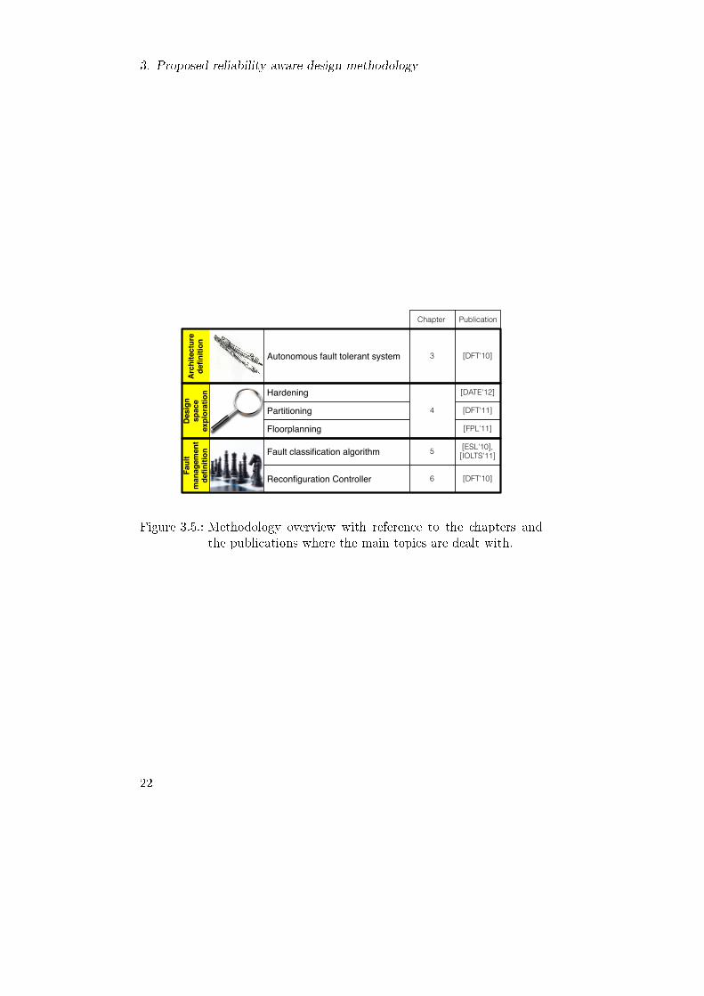
and (b) proposed fault management strategy. . . . . . . . 203.5. Methodology overview with reference to the chapters and
the publications where the main topics are dealt with. . . 22
4.1. Proposed design �ow. . . . . . . . . . . . . . . . . . . . . . 244.2. A schematic FPGA structure. . . . . . . . . . . . . . . . . 274.3. Multi-FPGA platform model. . . . . . . . . . . . . . . . . 284.4. The adopted recovery strategy for non-recoverable faults. . 334.5. TMR technique: di�erent application schemas. . . . . . . 344.6. Comparison between 1D and 2D recon�guration schemas. 434.7. Recon�gurable area de�nition: (a) correct speci�cation,
(b) area that does not contain the required resources, and(c) area that does not satisfy the recon�guration constraints. 44
4.8. Design �ow for �xed number of non-recoverable faults. . . 46
5.1. First proposal of fault classi�cation algorithm. . . . . . . . 515.2. Cause-based fault classi�cation in the space environment. 525.3. Second proposal of fault classi�cation algorithm. . . . . . 555.4. Second preliminary algorithm robustness evaluation. . . . 585.5. Fault Classi�er behavior . . . . . . . . . . . . . . . . . . . 595.6. Non-recoverable fault classi�cation . . . . . . . . . . . . . 605.7. Non-recoverable faults' timeline. . . . . . . . . . . . . . . . 635.8. Comparison of the number of fault observations to recog-
nize a non-recoverable fault in the proposed solution andthe second preliminary version of the algorithm. . . . . . . 68
6.1. First prototype of Recon�guration Controller. . . . . . . . 736.2. Software-based implemented prototype platform. . . . . . 73
XV
List of Figures
6.3. Reliable system. . . . . . . . . . . . . . . . . . . . . . . . . 746.4. Recon�guration Controller �ow diagram. . . . . . . . . . . 756.5. Preliminary Recon�guration Controller block diagram. . . 766.6. Proposed Recon�guration Controller block diagram. . . . 796.7. Fault Classi�er structure. . . . . . . . . . . . . . . . . . . 816.8. Fault Classi�er FSM. . . . . . . . . . . . . . . . . . . . . . 816.9. Fault Classi�er behavior when monitoring 10 areas and a
non-recoverable fault occurs on area #3. . . . . . . . . . . 826.10. Manager FSM. . . . . . . . . . . . . . . . . . . . . . . . . 836.11. Fault Classi�er with DWC. . . . . . . . . . . . . . . . . . 856.12. SC Fault Classi�er. . . . . . . . . . . . . . . . . . . . . . . 866.13. SC Fault Classi�er with TMR on the critical registers. . . 87
7.1. Multi-FPGA platform model. . . . . . . . . . . . . . . . . 927.2. Case study circuit. . . . . . . . . . . . . . . . . . . . . . . 937.3. Proposed design �ow. . . . . . . . . . . . . . . . . . . . . . 957.4. Case study circuit partitioning on the selected multi-FPGA
platform. . . . . . . . . . . . . . . . . . . . . . . . . . . . 967.5. TMR technique: di�erent application schemas [1]. . . . . . 987.6. Groups composing the hardened circuit. . . . . . . . . . . 1007.7. Hardened circuit partitioning on the selected multi-FPGA
platform when privileging the minimization of the externalcommunication. . . . . . . . . . . . . . . . . . . . . . . . . 102
7.8. Hardened circuit partitioning on the selected multi-FPGAplatform when considering a trade-o� of the metrics. . . . 102
7.9. Floorplan of each hardened sub-circuit on the related FPGA.1037.10. Alternative design �ow. . . . . . . . . . . . . . . . . . . . 1047.11. Preliminary grouping on case study circuit. . . . . . . . . 1057.12. Partitioning of hardened circuit in alternative design �ow. 1077.13. Floorplan of each hardened sub-circuit on the related FPGA
in alternative design �ow. . . . . . . . . . . . . . . . . . . 1087.14. Design �ow for �xed number of non-recoverable faults. . . 1097.15. Reliability-aware partitioning of the case study circuit when
following the design �ow for �xed number of non-recoverablefaults. . . . . . . . . . . . . . . . . . . . . . . . . . . . . . 110
A.1. Multi-FPGA platform model. . . . . . . . . . . . . . . . . 116
B.1. Case study circuit partitioning on the selected multi-FPGAplatform by setting wgap = 0.7, wwires = 0.2, and wcomm =0.1. . . . . . . . . . . . . . . . . . . . . . . . . . . . . . . . 119
XVI

List of Figures
B.2. Case study circuit partitioning on the selected multi-FPGAplatform by setting wgap = 0.7, wwires = 0.1, and wcomm =0.2. . . . . . . . . . . . . . . . . . . . . . . . . . . . . . . . 120
XVII

List of Tables
4.1. Multi-FPGA platform parameters. . . . . . . . . . . . . . 284.2. Preliminary partitioner constraints. . . . . . . . . . . . . . 314.3. Parameters used in the circuit hardening. . . . . . . . . . 354.4. Independently recoverable areas de�nition constraints. . . 374.5. Reliability-aware partitioner constraints. . . . . . . . . . . 41
5.1. Experimental setup parameters for the second preliminaryalgorithm evaluation. . . . . . . . . . . . . . . . . . . . . . 57
5.2. Probabilities Pr in the payload systems. . . . . . . . . . . 625.3. Orbits' λSEU . . . . . . . . . . . . . . . . . . . . . . . . . . 625.4. Predicted λrec at the considered environmental conditions. 635.5. Average Rmisr−nr by setting Pmisr−nr=0.005 . . . . . . . . 655.6. Average Rmisr−nr by setting n=5 . . . . . . . . . . . . . . 655.7. Average latency [hour] . . . . . . . . . . . . . . . . . . . . 67
6.1. Area occupation (slices and FFs � in parenthesis) of theFault Classi�er implementations and related overhead. . . 88
6.2. Area occupation (slices and FFs � in parenthesis) of theFault Classi�er modules for the nominal version and theSC one. . . . . . . . . . . . . . . . . . . . . . . . . . . . . 89
6.3. Area occupation of the Recon�guration Controller com-ponents' hardened implementations. . . . . . . . . . . . . 89
7.1. Resource requirements of the case study circuit. . . . . . . 947.2. Resource requirements of the case study circuit's hardened
components. . . . . . . . . . . . . . . . . . . . . . . . . . . 977.3. De�nition of the parameters max_faultsd for each FPGA
d. . . . . . . . . . . . . . . . . . . . . . . . . . . . . . . . . 977.4. De�nition of the independently recoverable areas for each
FPGA. . . . . . . . . . . . . . . . . . . . . . . . . . . . . . 997.5. De�nition of the parameters max_faultsd and #faultsd
for each FPGA d. . . . . . . . . . . . . . . . . . . . . . . . 1017.6. Alternative design �ow: De�nition of the independently
recoverable areas. . . . . . . . . . . . . . . . . . . . . . . . 106
XIX
List of Tables
7.7. De�nition of the parameters max_faultsd and #faultsd
for each FPGA d in alternative design �ow. . . . . . . . . 107
A.1. Values of partitioner's parameters. . . . . . . . . . . . . . 116A.2. Partitioner's execution times [s]. . . . . . . . . . . . . . . . 116
B.1. Partitioning solutions when privileging the distributionuniformity. . . . . . . . . . . . . . . . . . . . . . . . . . . . 118
B.2. Partitioning solutions when privileging the minimizationof external communication. . . . . . . . . . . . . . . . . . 118
B.3. Partitioning solutions when considering both the distribu-tion uniformity and the minimization of external commu-nication. . . . . . . . . . . . . . . . . . . . . . . . . . . . . 119
C.1. Values of partitioner's parameters. . . . . . . . . . . . . . 122C.2. Hardening approach's execution times [s]. . . . . . . . . . 122
D.1. Hardened solutions when privileging the distribution uni-formity. . . . . . . . . . . . . . . . . . . . . . . . . . . . . 124
D.2. Hardened solutions when privileging the maximization ofthe number of areas. . . . . . . . . . . . . . . . . . . . . . 125
D.3. Hardened solutions when privileging the minimization ofwires between groups. . . . . . . . . . . . . . . . . . . . . 125
D.4. Hardened solutions with a trade-o� between the metrics. . 126
XX
1. Introduction
In the last decades, Field Programmable Gate Arrays (FPGAs) have es-tablished themselves as target technology for both fast prototyping and�nal production of embedded systems. Among the many di�erent fami-lies, Static RAM (SRAM) FPGAs are the most used devices, since theyo�er various advantages with respect to other technologies. In particular,the most attractive feature of SRAM-based FPGAs is their �exibility, re-lated to the opportunity of re-programming (or recon�guring) the devicein a few clock cycles and on-line, while the device is operating. This al-lows the system implemented on the FPGA to be updated/upgraded,also remotely. For this reason, such devices are currently employed inmany applicative domains and their use is being investigated also formission-critical applications, for example the space ones, where the di-rect maintenance of the system is a di�cult task.Nevertheless, SRAM-based FPGAs are more susceptible to faults than
alternative solutions (for example, Application Speci�c Integrated Cir-cuits, ASICs), thus they can not be straightforward adopted for mission-critical applications unless reliability techniques are applied. In partic-ular for space applications, considered as target scenario of the thesis,reliability is a strict requirement due to the harsh environmental condi-tions and the di�culty of system maintenance. The widespread di�usionof this kind of devices has led to the investigation and de�nition of designtechniques and methodologies for hardening and recovering FPGA-basedsystems, with the �nal aim of exploiting such systems also in mission-critical scenarios. In general, hardening techniques are mostly based onspatial redundancy, whereas recovery ones exploit the FPGAs' recon-�guration capability, allowing to cope with the occurrence of faults byre-programming the faulty parts.Indeed, as hardened systems require many resources due to their size
and complexity, a single FPGA may not su�ce in terms of availableresources, and multi-FPGA solutions start being taken into account andinvestigated. Furthermore, the availability of more devices on multi-FPGA platforms could be exploited to implement a distributed enginedevoted to fault management. In fact, the use of multiple FPGAs providean increased reliability as the overall functionality is spread over multipledevices, possibly also using redundant implementations.
1
1. Introduction
While fault detection and masking techniques have been widely ad-dressed in the case of systems based on a single FPGA, the problemextended to multi-FPGA platforms has been rarely taken into account.The multi-FPGA scenario arises various issues, e.g. the partitioning ofthe system among the available devices, and the single FPGA approachescan not be straightforwardly adopted. In literature, no complete designmethodology handling all the peculiar issues of the considered scenariohas been proposed yet, a gap we aim at �lling with our work. In thisthesis, we de�ne a complete methodology for designing reliable embed-ded systems on multi-FPGA platforms. In the following, the proposedresearch is introduced. First, we will provide an overview of the researchand will highlight the main contributions of our work, presenting alsothe list of publications where the various aspects of the research havebeen presented.
1.1. Research overview and statement of
originality
The thesis proposes a reliability-aware methodology for designing embed-ded systems on multi-FPGA platforms, with the �nal aim of exploitingcommercial SRAM-based FPGAs for mission-critical applications. Theidea is to achieve fault tolerance against faults by exploiting the recon�g-urable properties of the devices. Two categories of faults are identi�ed,based on their impact on the device elements, such that a physical dam-age occurs or not; i) non-recoverable faults, that are those that causea permanent problem, making the portion of the fabric unusable, andii) recoverable faults, transient problems that can be �xed without caus-ing a lasting e�ect. Recoverable faults can be mitigated by recon�guringthe system (and possibly only the faulty sub-system portion) with thesame con�guration used before fault occurrence, whereas non-recoverablefaults, being characterized by a destructive e�ect, lead to the necessityof relocating the functionality to a non-faulty region of the device. Thedesigned system must be able to detect the occurrence of faults globallyand autonomously, in order to recover or to mitigate their e�ects. Thus,the methodology allows the overall system to continue working even iffaults occur, increasing both system reliability and lifetime.The main innovative contributions raised by this thesis are summarized
as follows:
• De�nition of an overall reliable multi-FPGA system with distributedcontrol architecture. Rather than making each FPGA an indepen-dent fault tolerant sub-system, able to locally detect and recover
2
1.1. Research overview and statement of originality
from faults, we have envisioned a distributed solution, where eachFPGA on the platform is in charge of monitoring and, in caseof fault, recon�guring the other devices. The aim is to achievea higher level of reliability in the overall system, trying to avoidthe single point of failure characterizing the centralized solutionand requiring to be implemented onto a particular device (e.g., anASIC or an antifuse-based FPGA).
• Management of both recoverable and non-recoverable faults. In lit-erature, only faults recoverable by recon�guring the FPGA areusually targeted, whereas faults physically damaging the deviceare rarely analyzed. Nevertheless, also faults of the latter typehave become relevant in the embedded systems design in the recentpast, due to the increasingly smaller device and wire dimensionsand higher operational temperatures, increasing the need to takethem into account next to the other faults. We propose a classi�-cation strategy and its companion algorithm for the discriminationof faults in FPGAs based on their impact on the device elementsand the consequent possibility to recover from them.
• Design of the engine in charge of implementing the suitable recoverystrategy based on the type of fault. We propose the design of thecontroller in charge of managing the fault recovery of the multi-FPGA platform, contributing to the creation of the reliable system.More precisely, we introduce a reliability-aware Recon�gurationController, aimed at performing the envisioned fault classi�cationand managing the recon�guration process of the faulty parts of thearchitecture to mitigate fault e�ects.
• De�nition of a complete �ow for designing autonomous fault toler-ant systems on multi-FPGA platforms. In literature, methodolo-gies for the design of autonomous fault tolerant systems on multi-FPGA platforms have not been proposed yet. We aim at �llingthis gap by introducing a complete �ow for designing such reli-able systems. Furthermore, we describe the developed prototypeframework, that implements the �ow and automates, as much aspossible, the design, hardening, and implementation of the envi-sioned systems.
The innovative points are covered throughout the thesis, that is struc-tured as follows. Chapter 2 presents the motivations of the proposedwork and introduces the background elements useful to set the basis forunderstanding the rest of the thesis. Chapter 3 describes the proposed
3
1. Introduction
reliability-aware design methodology, and Chapter 4 introduces the re-lated design �ow and prototype framework. Chapter 5 presents the clas-si�cation strategy and its companion algorithm for the discrimination offaults into recoverable and non-recoverable. Chapter 6 introduces thedesign of the reliability-aware Recon�guration Controller, aimed at per-forming the fault classi�cation and managing the recon�guration process.Chapter 7 discusses the methodology evaluation, performed by imple-menting a real case study. Finally, Chapter 8 closes the presentation ofthis research, drawing some conclusions and giving some possible futureresearch directions.
1.2. Publications
The various aspects of the research presented in this thesis have beenpublished in international conference proceedings and international jour-nals. The list of papers is the following.
DFT'10 Cristiana Bolchini, David Merodio Codinachs, Luca Fossati,Antonio Miele, Chiara Sandionigi, A reliable recon�guration con-troller for fault-tolerant embedded systems on multi-FPGA plat-forms, IEEE International Symposium on Defect and Fault Toler-ance in VLSI and Nanotechnology Systems, 2010, pp. 191-199
The paper presents the �rst proposal of the controller in charge ofmanaging the fault tolerance of multi-FPGA platform. The raisedinnovative points are the identi�cation of a distributed control ar-chitecture, allowing the avoidance of single points of failure, andthe de�nition of an overall reliable multi-FPGA system.
ESL'10 Cristiana Bolchini, Chiara Sandionigi, Fault classi�cation forSRAM-based FPGAs in the space environment for fault mitigation,IEEE Embedded Systems Letters, Volume 2, 2010, pp. 107-110
The letter describes the �rst proposal of fault classi�cation al-gorithm to discriminate between recoverable and non-recoverablefaults occurring in SRAM-based FPGAs. By considering space ap-plications, the controller de�nition starts from a characterizationof the radiation e�ects and aging mechanisms.
IOLTS'11 Cristiana Bolchini, David Merodio Codinachs, Luca Fossati,Chiara Sandionigi, A reliable fault classi�er for dependable systemson SRAM-based FPGAs, 17th IEEE International On-Line TestingSymposium, 2011, pp. 105-110
4
1.2. Publications
The paper presents an enhanced and formally evaluated fault clas-si�cation algorithm. With respect to previous approaches, includedthe one described in the previous letter, the main contributions ofthe work are the formal de�nition of the parameters characteriz-ing the algorithm, the evaluation of the conditions for correct faultclassi�cation, and the investigation of the reliable implementationof the classi�er.
DFT'11 Cristiana Bolchini, Chiara Sandionigi, A reliability-aware parti-tioner for multi-FPGA platforms, IEEE International Symposiumon Defect and Fault Tolerance in VLSI and Nanotechnology Sys-tems, 2011, Accepted, To appear
The paper presents a partitioning approach for reliable systemson multi-FPGA platforms. With respect to literature, where thepartitioning problem is solved by heuristic algorithms based onnon-accurate models, we have proposed a partitioner that identi�esthe global optimal solution in an acceptable execution time and canbe integrated in an overall reliability-aware design �ow.
From a wider point of view, part of the research here presented hasalso been exploited in the single FPGA scenario, when smaller systemsare considered, leading to the following publications.
TC'10 Cristiana Bolchini, Antonio Miele, Chiara Sandionigi, A noveldesign methodology for implementing reliability-aware systems onSRAM-based FPGAs, IEEE Transactions on Computers, 2010, Ac-cepted, To appear
The paper presents a methodology for the implementation of sys-tems on single SRAM-based FPGAs with soft error mitigationproperties. This is the �rst proposal of complete design �ow forrealizing reliable FPGA-based systems. The approach has beentaken into account and extended for the scenario envisioned in thethesis; more precisely, multi-FPGA platforms have been consideredfor the implementation of systems able to cope with both recover-able and non-recoverable faults.
ETS'10 Cristiana Bolchini, Antonio Miele, Chiara Sandionigi, NiccolóBattezzati, Luca Sterpone, Massimo Violante, An integrated �owfor the design of hardened circuits on SRAM-based FPGAs, 15thIEEE European Test Symposium, 2010, pp. 214-219
In this paper, the design �ow presented in the previous one hasbeen enhanced. The framework integrates strategies independently
5

1. Introduction
designed to tackle the problem of recoverable faults. Also this ap-proach has been considered and extended for the envisioned sce-nario.
FPL'11 Cristiana Bolchini, Antonio Miele, Chiara Sandionigi, Auto-mated resource-aware �oorplanning of recon�gurable areas in partially-recon�gurable FPGA systems, 21st International Conference onField Programmable Logic and Applications, 2011, pp. 532-538
The paper presents a �oorplanner for FPGA-based systems. Theproposed �oorplanner is based on an accurate model of the devicesand takes into account all the elements characterizing them, namelythe constraints imposed by the peculiar structure of the fabric andthe recon�guration capabilities.
Finally, the following paper has been submitted to international con-ference.
DATE'12 Cristiana Bolchini, Antonio Miele, Chiara Sandionigi, Increas-ing autonomous fault-tolerant FPGA-based systems' lifetime, Sub-mitted to Design, Automation and Test in Europe 2012
The paper proposes a methodology for the design of autonomousfault-tolerant FPGA systems, with the �nal objective of increasingthe system's lifetime and availability. The main contribution of thework is the design space exploration, that identi�es the most con-venient with the �nal aim of maximizing the number of toleratednon-recoverable faults.
6

2. Motivations and working
scenario
Our research proposes a methodology for designing reliable embeddedsystems on multi-FPGA platforms, with the �nal objective of increasingthe system's lifetime in critical scenarios. This chapter presents the mo-tivations of the proposed work and introduces the background elementsuseful to set the basis for understanding the rest of the thesis.The chapter is structured as follows: Section 2.1 discusses the moti-
vations leading to the proposed thesis. Section 2.2 introduces the faultmodel that has been adopted as a reference for the de�nition of thereliability-aware design methodology. Section 2.3 re�nes the model byreferring to the working scenario, namely the space environment, consid-ered for its stringent reliability requirements due to the harsh environ-mental conditions, the long lifetime of space missions, and the di�cultof system maintenance. Finally, Section 2.4 draws the chapter summary.
2.1. Motivations
During the last decades, FPGAs have been adopted as a target technol-ogy for both the fast prototyping and �nal production of embedded sys-tems. Among the many di�erent FPGA families, SRAM-based ones arethe most used platforms, due to various advantages they present with re-spect to alternative solutions. Compared to traditional microprocessors,they reveal higher computational capability, lower power consumption,and lower cost [2]. Moreover, thanks to the ability of changing theirbehavior over time (feature often referred to as �recon�gurability�), theyprovide an increased �exibility with respect to alternative hardware solu-tions, like Application Speci�c Integrated Circuits (ASICs) and antifuse-based FPGAs, that can be programmed only once. In fact, SRAM-basedFPGAs can be reprogrammed in a few clock cycles and on-line, whilethe device is operating. The advent of such dynamically recon�gurablehardware into the embedded systems domain allows for exploiting theperformance of hardware along with the adaptability of software; re-con�gurable devices may achieve performance similar to hardware whilebeing as �exible as software, given that they can change the function
7

2. Motivations and working scenario
they perform. As such, recon�gurable devices are a �rst class choicefor combining both adaptability and performance. Devices similar toSRAM-based FPGAs are Flash-based FPGAs, enabling device recon�g-uration through the use of non-volatile con�guration memory; neverthe-less, such technology presents lower throughput, smaller amount of logic,and higher costs. For these reasons, SRAM-based FPGAs are currentlyemployed in many applicative domains.Given their peculiarities, SRAM-based FPGAs could be an attrac-
tive technology not only for the standard commercial market, but alsoin mission- or safety-critical applications; for instance, the space envi-ronment, considered as a possible application scenario for this work, isparticularly critical for the harsh operating conditions and the not af-fordable maintenance. Nevertheless, such devices are more susceptibleto faults with respect to traditional solutions (e.g., ASICs) [3], thus faultmitigation and recovery techniques are paramount to guaranteeing thatthe system will work correctly. For this class of devices, in general, faultdetection/tolerance strategies are mostly based on spatial redundancy,whereas recovery ones exploit the device's recon�guration capabilitiesby performing scrubbing, readback or even partial recon�guration of thefaulty parts [4]. When a fault is detected, the a�ected functionalityis re-created on the FPGA, thus restoring the device's overall process-ing capabilities. Traditionally, the major source of concerns has beenmainly represented faults causing errors in the memories devoted to theapplication data and con�guration. These errors can be easily �xed byrewriting the correct information. Nevertheless, also faults physicallydamaging the device have become relevant for digital systems in the re-cent past; in fact, as highlighted in 2003 by the International Road Mapof Semiconductors [5], such faults will have a higher impact due to theincreasingly smaller device and wire dimensions and higher operationaltemperatures, raising the need to take them into account next to theother faults.Another aspect gaining importance is the limited amount of function-
alities FPGAs can accommodate. Indeed, as the size and complexity ofthe systems being designed increase (in particular after the applicationof fault tolerance techniques), a single FPGA may not su�ce in terms ofavailable resources, and multi-FPGA solutions start being taken into ac-count and investigated (e.g., [6, 7, 8, 9]). Furthermore, the availability ofmore devices on multi-FPGA platforms could be exploited to implementa distributed engine devoted to fault management.While fault detection and masking techniques have been widely ad-
dressed in the case of systems based on a single FPGA (e.g., [10, 11, 4]),the problem extended to multi-FPGA platforms has been rarely taken
8

2.2. Fault model
into account. Moreover, only faults recoverable by recon�guring thedevice are usually targeted ([4, 12, 11]), whereas faults physically dam-aging the device are rarely analyzed. The approach in [1] presents adesign �ow for implementing digital systems on single SRAM-based FP-GAs with soft error mitigation properties. While it could be adaptedto multi-FPGA platforms and extended to faults with destructive e�ect,we claim that an ad-hoc solution for this scenario would consistentlyimprove the system's performance and its reliability. In literature, whenconsidering multi-FPGA platforms, the available devices are usually ex-ploited to host replicas of the main system, as in [8], where three FPGAsare used to apply the classical Triple Modular Redundancy (TMR) tech-nique on the whole circuit. Each FPGA hosts the same con�gurationand a controller, implemented on an external radiation-hardened ASIC,acts as a TMR voter. Indeed, this is a di�erent scenario with respectto the one we envision; we aim at better exploiting the devices potentialand providing a scalable solution, independent of the number of FPGAsused. In addition, the controller needs to be implemented on particularASIC technology, eliminating most of the advantages of having SRAM-based FPGAs in the system, namely �exibility and relatively low cost.To conclude, no complete design methodology handling all the peculiarissues of the considered scenario has been proposed yet, a gap we aim at�lling with our work.In this thesis, we de�ne a complete methodology for designing reliable
embedded systems on multi-FPGA platforms. The �nal objective is theexploitation of commercial SRAM-based FPGAs for mission-critical ap-plications, realizing reliable systems that autonomously cope with bothfaults recoverable by recon�guration and faults physically damaging thedevice. In the next section, we introduce the adopted fault model, thatis at the basis of the proposed methodology.
2.2. Fault model
When designing fault mitigation strategies, the single fault assumptionis traditionally considered. We adopt such assumption because realisticfor the considered scenario. It implies that i) faults occur one at atime and ii) the time between the occurrence of two subsequent faultsis long enough to allow the detection of the �rst fault before the secondone occurs. Indeed, the fault only produces an observable e�ect, anerror, if i) the fault occurs in a used resource and ii) the applied input(sequence) is such that a di�erence in the data/behavior is caused withrespect to the fault-free situation. Thus, since it may happen that not all
9
2. Motivations and working scenario
available resources are actually used, the observability of a fault is relatedto the probability of the fault to hit a used resource. Furthermore, itis necessary that the adopted detection mechanism identi�es the faultsituation with short latency between the fault occurrence and the errordetection.It is worth noting that the single fault assumption prevents dealing
with faults accumulation, possibly leading to the failure of fault tolerancetechniques due to masking/biasing e�ects. In general, though, since theproposed system is divided into areas, as described in Chapter 3, faultmitigation techniques can also deal with multiple faults, provided theyoccur in independent portions of the entire system. A full extension tomultiple faults management will be considered in future work, althoughfor some sets of multiple failures the proposed approach holds.When considering SRAM-based FPGAs, it is possible to identify two
types of memory that can be subject to faults; the one storing the ap-plication data being processed and the one storing the con�guration bit-stream, that de�nes the functionality performed by the recon�gurablefabric. If the data memory is corrupted, an erroneous value is produced,whereas, when a fault corrupts a con�guration memory element, it mod-i�es the programmed functionality. Con�guration memory accounts tomore than 95% of the fraction of the device sensitive to faults [12], thusan erroneous functionality is the most common produced e�ect. Never-theless, we aim at covering faults a�ecting both kinds of memories. Tocope with erroneous values, a reset of the application can be performedor feedback loops to propagate the correct values to the registers can beadded, whereas, to restore erroneous functionalities, the con�gurationmust be re-written.In the next section, we provide a more detailed characterization of
faults by referring to the considered working scenario, namely the spaceenvironment.
2.3. Working scenario: the space environment
The working scenario of this thesis is the space environment, selectedfor the stringent reliability requirements of space applications due to theharsh environmental conditions and the di�culty of system maintenance.In fact, the massive presence of radiations possibly causes glitches inthe system elaboration, and maintainability operations are very di�cultwhen considering that the communication with Earth is limited in bothavailability and bandwidth, necessary to remotely cope with unpredictedfailure situations. Two problems have been identi�ed as main causes of
10
2.3. Working scenario: the space environment
faults in space; radiations and device aging. In the following, they areanalyzed in relation to the selected platform, SRAM-based FPGAs, byidentifying their main e�ects and characteristics. Finally, the adoptedfault classi�cation is presented.
2.3.1. Radiation e�ects
Radiations are the most common cause of faults in space. They consist ofdi�erent particles, mainly electrons, protons and heavy ions, originatedfrom various sources, e.g. the sun, novas, and supernovas. Their energylevels depend on the source and the orbit; in Van Allen belts region,radiations' electrons and protons have energies up to tens and hundredsof MeV, respectively, whereas solar cosmic rays have energies up to GeV,and the galactic cosmic rays up to TeV [13]. Radiations, when hittingan electronic device, can cause a problem mainly observable in memoryelements implemented with static cells. The e�ects can be divided intotwo main groups [14]:
• Single Event E�ect (SEE), that is a measurable e�ect resultingfrom the deposition of energy from a single ionizing particle strike,and
• Total Ionizing Dose (TID) e�ect, that is a cumulative long termionizing damage mostly due to protons and electrons.
SEEs can take many forms. They are distinguished into non-destructiveor destructive, based on their e�ect; non-destructive SEEs can be recov-ered by resetting or recon�guring the device, whereas destructive SEEshave a persistent e�ect even after a reset or a recon�guration since thedevice is permanently damaged by the radiation. Non-destructive SEEsdue to radiations are commonly called Single Event Upsets (SEUs),modeled as bit �ips. Particular types of SEUs are Single Event Dis-turbs (SEDs), momentary voltage excursions at nodes, and Single EventFunctional Interrupts (SEFIs), interrupts leading to temporary non-functionality of the a�ected device by involving power-on-reset, Selectmap port or JTAG port. SEDs are treated as general SEUs, whereasSEFIs are not taken into account in this thesis since they are negligiblein occurrence [15]. Other SEEs have the potential to destroy the de-vice. Destructive SEEs are Single Event Latchups (SELs), energy froma charged particle leading to an excessive supply power. They are nottaken into account in this work as test reports on SRAM-based FPGAsreveal that no SEL was observed during the experiments, up to the max-imum tested Linear Energy Transfer of tens of MeV · cm2/mg [16, 17],that is su�cient for the considered applications.
11
2. Motivations and working scenario
Also TID e�ects have the potential to destroy the device. TID de�nesthe total sum of radiations hitting the device. The unit of measurementin the International System of Units is the Gray (Gy), de�ned by theamount of 1 Joule of energy deposited per kilogram, however the depre-cated unit rad (radiation absorbed dose) is still frequently used [14].
2.3.2. Aging e�ects
Device aging is the other analyzed cause, an important aspect for long-lasting space missions, where system maintenance or substitution is dif-�cult. Aging causes the following faults with destructive e�ect [18, 19]:
• Time Dependent Dielectric Breakdown (TDDB), that is a break-down caused by charge �ow through the oxide,
• Electromigration (EM), that is a development of voids in metallines due to heavy current densities over a period of time,
• Hot-Carrier E�ects (HCE), that are interface traps a�ecting theI-V characteristics of the transistors, and
• Negative Bias Temperature Instability (NBTI), that is the degra-dation dependent on the time a PMOS transistor is stressed in thecircuit.
In the �eld of FPGAs, these faults are just being recently addressed, alsodue to their rareness.
2.3.3. Adopted fault classi�cation
We identify two categories of faults based on the possibility to recoverfrom them by recon�guration; recoverable and non-recoverable faults.Recoverable faults can be mitigated by recon�guring the system, andpossibly only the faulty sub-system portion, with the same con�gura-tion used before fault occurrence. Non-recoverable faults permanentlycompromise part or all of the device, such that further use of the cor-rupted portion of the device must be avoided and the logic hosted mustbe moved in a di�erent location. The identi�cation of the type of faultoccurred on the device is thus fundamental to apply the suitable recoverystrategy.To summarize, recoverable faults are the ones caused by radiations
without a destructive e�ect, whereas non-recoverable faults are thosecaused by radiations with destructive e�ect, radiations' accumulationand device aging. Figure 2.1 shows such fault classi�cation based on theanalyzed causes and e�ects.
12
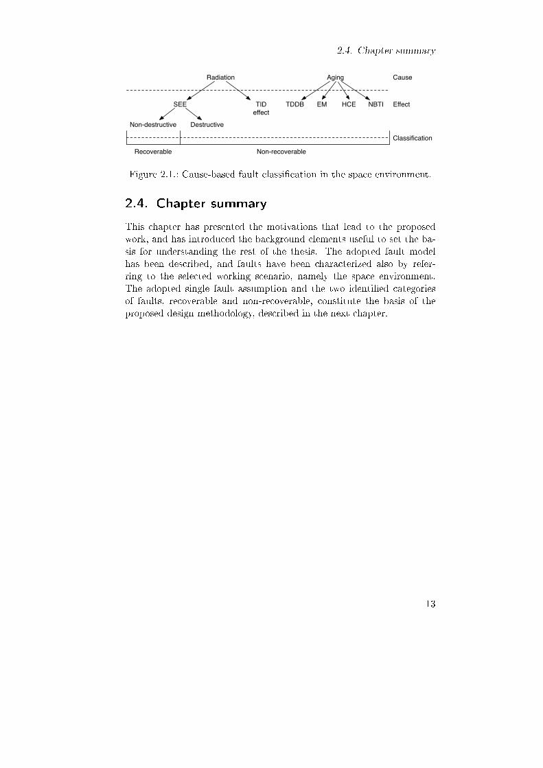
2.4. Chapter summary
Radiation Aging
TIDeffect
NBTISEE TDDB
Non-destructive Destructive
Recoverable Non-recoverable
Cause
Effect
Classification
EM HCE
Figure 2.1.: Cause-based fault classi�cation in the space environment.
2.4. Chapter summary
This chapter has presented the motivations that lead to the proposedwork, and has introduced the background elements useful to set the ba-sis for understanding the rest of the thesis. The adopted fault modelhas been described, and faults have been characterized also by refer-ring to the selected working scenario, namely the space environment.The adopted single fault assumption and the two identi�ed categoriesof faults, recoverable and non-recoverable, constitute the basis of theproposed design methodology, described in the next chapter.
13


3. Proposed reliability-aware
design methodology
The wide use of FPGAs in critical scenarios, such as long-term spacemissions, leads to the necessity of design methodologies for the realiza-tion of systems able to autonomously cope with the occurrence of bothrecoverable and non-recoverable faults. Indeed, the scenario is even morecomplex when systems of considerable size are taken into account, re-quiring the use of several FPGAs at once. However, no complete designmethodology handling all the peculiar issues has been proposed yet, agap we aim at �lling with our work. More precisely, in this chapter,we introduce a methodology for the design of autonomous fault toler-ant systems implemented on multi SRAM-based FPGAs, with the �nalobjective of increasing the system's lifetime and availability.The chapter is structured as follows: Section 3.1 presents the proposed
design methodology. Section 3.2 describes the devised reliable systemand Section 3.3 shows the behavior of the proposed system in variousfault scenarios. Finally, Section 3.4 draws the chapter summary.
3.1. Reliability-aware design methodology
The proposed reliability-aware methodology realizes autonomous faulttolerant systems implemented on multi-FPGA platforms, with the �-nal objective of exploiting commercial SRAM-based FPGAs for mission-critical applications. While some aspects can be taken from previoussolutions available in literature, several open issues for the proposedmethodology exist and have been investigated. They can be summa-rized as follows:
• Reliability-aware architecture de�nition. First of all, it is neces-sary to establish how to exploit the available SRAM-based FPGAsto build the autonomous fault tolerant system. The architectureimplementing the system must be de�ned; the communication be-tween FPGAs for data exchanging and con�guration must be iden-ti�ed and the controller solution must be selected.
15

3. Proposed reliability-aware design methodology
• Reliability-aware circuit hardening and distribution. The nominalapplication circuit must be hardened and distributed among theFPGAs available on the platform. A set of metrics guiding in thede�nition of the reliable solution must be selected, and a strategyfor identifying the most promising solution must be de�ned.
• Fault classi�cation strategy and Recon�guration Controller design.It is necessary to de�ne a policy to classify the faults occurred inthe system as recoverable or non-recoverable, based on the factthat the portion of the device is not actually compromised andthus will not properly work. Furthermore, it is necessary to designthe engine in charge of implementing the recovery strategy. Thecontroller must be able to monitor a parametric number of errorsignals, generated by a not known a-priori number of other FPGAsin the architecture, and, based on the identi�ed type of fault, itmust perform the suitable recovery action.
The proposed methodology aims to cope with these open points. It iscomposed of the following main activities, each of them trying to �x oneof the described issues, as shown in Figure 3.1:
• Architecture de�nition. This activity de�nes and characterizes theautonomous fault tolerant system. It identi�es the platform topol-ogy; given the available FPGAs, it establishes how they are con-nected to each other for communication and con�guration. More-over, it de�nes the controller solution, that could be centralized ona single device or distributed among the available FPGAs.
• Design space exploration. This is the core of the proposed method-ology; this activity is devoted to the hardening of the nominal cir-cuit on the multi-FPGA platform. As the name suggests, we arenot just pursuing a working solution, rather the one o�ering themost convenient trade-o� with respect to the designer's selectedmetrics. The activity is composed of three main steps: i) harden-ing, that selects and applies fault detection/tolerance techniques,ii) partitioning, that distributes the obtained reliable circuit amongthe available FPGAs, and iii) �oorplanning, that positions eachsub-circuit within the related device. A design space explorationis performed to identify the most promising solution according toa selected set of metrics.
• Fault management de�nition. This activity identi�es how to clas-sify the faults and cope with their occurrence. It de�nes the con-
16
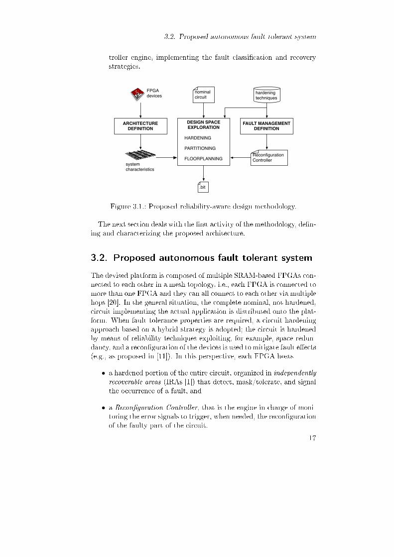
3.2. Proposed autonomous fault tolerant system
troller engine, implementing the fault classi�cation and recoverystrategies.
FPGAdevices
ARCHITECTURE DEFINITION
FAULT MANAGEMENT DEFINITION
DESIGN SPACEEXPLORATION
nominal circuit
.bit
hardening techniques
Reconfiguration Controller
systemcharacteristics
HARDENING
PARTITIONING
FLOORPLANNING
Figure 3.1.: Proposed reliability-aware design methodology.
The next section deals with the �rst activity of the methodology, de�n-ing and characterizing the proposed architecture.
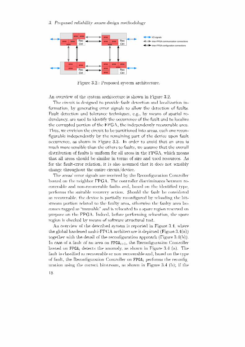
3.2. Proposed autonomous fault tolerant system
The devised platform is composed of multiple SRAM-based FPGAs con-nected to each other in a mesh topology, i.e., each FPGA is connected tomore than one FPGA and they can all connect to each other via multiplehops [20]. In the general situation, the complete nominal, not hardened,circuit implementing the actual application is distributed onto the plat-form. When fault tolerance properties are required, a circuit hardeningapproach based on a hybrid strategy is adopted; the circuit is hardenedby means of reliability techniques exploiting, for example, space redun-dancy, and a recon�guration of the devices is used to mitigate fault e�ects(e.g., as proposed in [11]). In this perspective, each FPGA hosts
• a hardened portion of the entire circuit, organized in independentlyrecoverable areas (IRAs [1]) that detect, mask/tolerate, and signalthe occurrence of a fault, and
• a Recon�guration Controller, that is the engine in charge of moni-toring the error signals to trigger, when needed, the recon�gurationof the faulty part of the circuit.
17
3. Proposed reliability-aware design methodology
Rec Ctrl
Rec Ctrl
Rec Ctrl
Inter-FPGA communication connections
Inter-FPGA configuration connections
I/O signals
areaarea area
area
area
area
area
area
area
area
areaarea
Rec Ctrl area
area
areaarea areaarea
Figure 3.2.: Proposed system architecture.
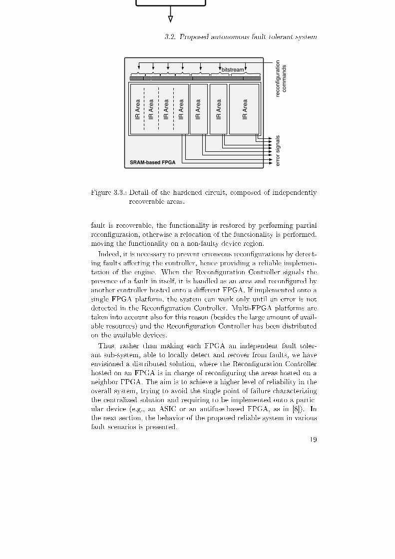
An overview of the system architecture is shown in Figure 3.2.The circuit is designed to provide fault detection and localization in-
formation, by generating error signals to allow the detection of faults.Fault detection and tolerance techniques, e.g., by means of spatial re-dundancy, are used to identify the occurrence of the fault and to localizethe corrupted portion of the FPGA, the independently recoverable area.Thus, we envision the circuit to be partitioned into areas, each one recon-�gurable independently by the remaining part of the device upon faultoccurrence, as shown in Figure 3.3. In order to avoid that an area ismuch more sensible than the others to faults, we assume that the overalldistribution of faults is uniform for all areas in the FPGA, which meansthat all areas should be similar in terms of size and used resources. Asfor the fault-error relation, it is also assumed that it does not sensiblychange throughout the entire circuit/device.The areas' error signals are received by the Recon�guration Controller
hosted on the neighbor FPGA. The controller discriminates between re-coverable and non-recoverable faults and, based on the identi�ed type,performs the suitable recovery action. Should the fault be consideredas recoverable, the device is partially recon�gured by reloading the bit-stream portion related to the faulty area, otherwise the faulty area be-comes tagged as �unusable� and is relocated to a spare region reserved onpurpose on the FPGA. Indeed, before performing relocation, the spareregion is checked by means of software structural test.An overview of the described system is reported in Figure 3.4, where
the global hardened multi-FPGA architecture is depicted (Figure 3.4(a))together with the detail of the recon�guration approach (Figure 3.4(b)).In case of a fault of an area on FPGAi+1, the Recon�guration Controllerhosted on FPGAi detects the anomaly, as shown in Figure 3.4 (a). Thefault is classi�ed as recoverable or non-recoverable and, based on the typeof fault, the Recon�guration Controller on FPGAi performs the recon�g-uration using the correct bitstream, as shown in Figure 3.4 (b); if the
18
3.2. Proposed autonomous fault tolerant system
7
SR
AM
-bas
ed F
PG
A
rad-hard FPGA
primary inputs
primary outputs
error signals
reconfigurationcommands fault manager
&reconfiguration
controller
hardenedsystems
withfault detection fault masking
properties
(a)
erro
r sig
nals
reco
nfigu
ratio
nco
mm
andsbitstream
IR A
rea
IR A
rea
IR A
rea
IR A
rea
IR A
rea
IR A
rea
IR A
rea
SRAM-based FPGA
(b)
Fig. 6. a) The reliability-aware system architecture, and b) the detail of the
hardened system: fault management to determine fault occurrence and partial
reconfiguration of the corrupted portion of FPGA device.
their characteristics in terms of costs and benefits, and their
impact on the circuit structure. Given such a model, it is possi-
ble to automate the application of the techniques allowing the
generation and the evaluation of different solutions, and, thus,
enabling the design space exploration. The model provides
the description of the techniques in terms of a combination
of various aspects; the achieved fault management capability,
a set of modifications on the circuit structure, and a set of
mapping constraints, described in the following.
First of all, techniques can be classified based on the faultmanagement property they offer, fault detection or fault tol-
erance. Moreover, since these techniques are based on redun-
dancy (mainly in space), each one of them is characterized by
a modification of the circuit due to the introduction of replicas
of the functional units and checking/voting components. Cost
characterization for these specific elements are provided by
the technique model itself, and are stored in the repository.
The number of IR Areas (Fig. ??b) is one of the elements
to be evaluated during the design exploration phase, since
as it grows it allows for a more precise fault localization
and consequently a reduced reconfiguration action (with low
time and power overheads); however, as the number increases,
the amount of voted/compared lines increases as well, raising
area overheads and introducing performance degradation. In
particular, these IR Areas are the result of the application
of the classical techniques with two additional elements:
components’ grouping and reconfigurable area mapping. More
precisely, when applying fault management techniques, the
two alternatives usually adopted either consider the entire
system as a unique entity, system level granularity, or work on
the single component, component level granularity. However,
it is also possible to gather components into groups, and apply
a technique with respect to such groups, thus obtaining a
C1
C2
C3
data_outdata_in
NominalC1
C2
C3
F
VOTER+
C1
C1
C1
VOTER+
C2
C2
C2
C3
C3
C3
VOTER+
VOTER+
n
m
m
n
k
n+m
System level Component level
C1
C1
C1
VOTER
C2
C3
C2
C3
C2
C3
VOTER+
n+m
kk
n+m
Group 1
Group 2
Group 1
Group 3
Group 2Group 1
(a) (b) (c)
C1
C2
C3
C1
C2
C3
Fig. 7. TMR application at different granularity levels: from (a) system level
to (c) component level (the three voters have been designed as a single module
for clarity reasons).
hardened implementation characterized by costs and benefits
that are a trade-off with respect to the two basic application
strategies ([?], [?]). In particular, components’ grouping allows
for a reduction in the number of voted/compared lines and
in a more precise fault localization capability, which can be
used to better focus the recovery action. Fig. ?? reports, as
an example, the application of the classical TMR technique
at different granularity levels, from system (Fig. ??a) to
component (Fig. ??c), considering also intermediate solutions
(Fig. ??b).
Finally, given a technique, a few mapping schemas can be
adopted for the hardened circuit; the trivial approach places
each hardened circuit on a unique IR Area, whose size, shape
and localization have to satisfy the device constraints. How-
ever, when considering some techniques, the different replicas
can also be mapped onto different IR Areas in different ways,
as shown in Fig. ?? for the TMR technique.
Altogether, components’ grouping and reconfigurable area
mapping determine how a technique is applied, and it is the
design exploration phase that analyzes the various possibilities
to identify those implementations that minimize the cost
functions the designer deems as important.
A peculiarity of the proposed framework is the flexibility
of the techniques’ repository: techniques are not hardcodedin the algorithm implementing the design space exploration
but are modeled in terms of costs and impacts on the circuit.
Therefore, the list of techniques can be extended with new
ones but also reduced, allowing also the designer to (tem-
porarily) use only some techniques, providing a particularly
versatile approach. In the following paragraphs the model of
the considered techniques.
1) Duplication With Comparison (DWC): It aims at guar-
anteeing fault detection capabilities. It consists of adding a
replica of the functional unit and introducing a comparator;
the replica actually computes complemented values and the
comparator is implemented with a Two-Rail Checker (TRC)
[?], a Totally Self-Checking circuit able to detect differences
between the outputs of the nominal and duplicated units. Two-
Rail Checkers produce two output signals, adopting an odd-
parity code; {01,10} imply a fault-free situation, whereas
{00,11} denote the occurrence of a fault, either in one of
the two replicas or in the checker itself. For the technique
only one mapping strategy is adopted, which places the whole
Figure 3.3.: Detail of the hardened circuit, composed of independentlyrecoverable areas.
fault is recoverable, the functionality is restored by performing partialrecon�guration, otherwise a relocation of the functionality is performed,moving the functionality on a non-faulty device region.
Indeed, it is necessary to prevent erroneous recon�gurations by detect-ing faults a�ecting the controller, hence providing a reliable implemen-tation of the engine. When the Recon�guration Controller signals thepresence of a fault in itself, it is handled as an area and recon�gured byanother controller hosted onto a di�erent FPGA. If implemented onto asingle FPGA platform, the system can work only until an error is notdetected in the Recon�guration Controller. Multi-FPGA platforms aretaken into account also for this reason (besides the large amount of avail-able resources) and the Recon�guration Controller has been distributedon the available devices.
Thus, rather than making each FPGA an independent fault toler-ant sub-system, able to locally detect and recover from faults, we haveenvisioned a distributed solution, where the Recon�guration Controllerhosted on an FPGA is in charge of recon�guring the areas hosted on aneighbor FPGA. The aim is to achieve a higher level of reliability in theoverall system, trying to avoid the single point of failure characterizingthe centralized solution and requiring to be implemented onto a partic-ular device (e.g., an ASIC or an antifuse-based FPGA, as in [8]). Inthe next section, the behavior of the proposed reliable system in variousfault scenarios is presented.
19

3. Proposed reliability-aware design methodology
Rec Ctrl 2
Hardened sub-system
3
Rec Ctrl 3
Rec Ctrl 4
Hardened sub-system
1
Hardened sub-system
4
Rec Ctrl 1
Rec Ctrl 2
Hardened sub-system
1
Rec Ctrl 1
areaA
Chk
Recoverablefault
Non-recoverablefault
(a) (b)
areaBareaC
areaAareaBareaCareaB
Figure 3.4.: Target scenario: (a) hardened multi-FPGA architecture and(b) proposed fault management strategy.
3.3. Additional fault scenarios
The proposed methodology implements a reliable system on multi-FPGAplatform with the �nal objective of increasing its lifetime and availability.As described in the previous chapter, in designing the system, the singlefault assumption is adopted, implying that faults occur one at a timeand the time between the occurrence of two subsequent faults is longenough to allow the detection of the �rst fault before the second oneoccurs. However, we hereby consider other possible fault scenarios anddiscuss how the proposed methodology behaves.
• Multiple faults. The proposed methodology can also deal withmultiple faults, provided they do not lead to the failure of faultdetection techniques or they occur in independent portions of theentire system. We envision two scenarios, where multiple faultsoccur i) on the same single FPGA or ii) on di�erent devices. Inthe former case, the overall system would be able to cope withthis situation, and the designed controller would manage the con-current faults in di�erent areas. Nevertheless, it is worth notingthat the proposed Recon�guration Controller and the implementedfault classi�cation algorithm, described in the next chapters, havebeen designed based on the single fault assumption. Therefore,we expect tolerable glitches in the classi�cation possibly leadingto delays in tolerating a non-recoverable fault, as discussed in theupcoming chapter. In the latter case, faults occurred on di�erentFPGAs are recovered by the controllers in charge of monitoring thedevices, preventing a failure of the entire system. A failure couldoccur when no recovery action can be performed due to faults con-temporarily a�ecting all controllers; indeed, this is a rare, negligiblesituation.
20
3.4. Chapter summary
• Failure of the recon�guration process. An error can occur duringthe recon�guration process, triggered by the occurrence of a faultin the monitored FPGA. This can happen because of i) a faultin the Recon�guration Controller or ii) a fault in the inter-FPGAcommunication. In the former case, the recon�guration is blockedas soon as an erroneous behavior of the Recon�guration Controlleris observed and the fault is recovered by the controller on the neigh-bor FPGA. In the latter case, no recovery action can be performedfor the faulty FPGA and the system gradually degrades.
To conclude, although the proposed methodology is based on the tra-ditionally adopted single fault assumption, the obtained reliable systemcan also deal with other more complex and not frequent fault scenarios.
3.4. Chapter summary
In this chapter, we have introduced the methodology we devised for thedesign of autonomous fault-tolerant FPGA-based systems. We exploitmulti-FPGA platforms to build reliable systems able to autonomouslycope with both recoverable and non-recoverable faults, with the �nalobjective of increasing the system's lifetime. Di�erently from the pastapproaches, rather than making each FPGA an independent fault toler-ant sub-system, able to locally detect and recover from faults, we haveenvisioned a distributed controller solution. Although the methodologyconsiders the traditionally adopted single fault assumption, the obtainedsolution can also deal with other, infrequent fault scenarios.In the rest of the thesis, the methodology's activities are described
in detail. Figure 3.5 provides an overview of the methodology, withreference to the chapters and publications where the main topics are dealtwith (refer to Chapter 1 for the list of publications). The architecturede�nition activity has already been presented in Section 3.2. The nextchapter introduces the proposed design �ow for obtaining the reliablesystem.
21
3. Proposed reliability-aware design methodology
Autonomous fault tolerant system
Fault classification algorithm
Reconfiguration Controller
Hardening
Partitioning
Floorplanning
Chapter Publication
3 [DFT'10]
4
5
6
[ESL'10],[IOLTS'11]
[DFT'10]
[DATE'12]
[DFT'11]
[FPL'11]
Arc
hite
ctur
e de
finiti
onFa
ult
man
agem
ent
defin
ition
Des
ign
spac
e ex
plor
atio
n
Figure 3.5.: Methodology overview with reference to the chapters andthe publications where the main topics are dealt with.
22
4. Design �ow and framework
The methodology introduced in the previous chapter aims at realizingsystems able to autonomously cope with the occurrence of both recov-erable and non-recoverable faults. An autonomous fault tolerant multi-FPGA system has been proposed, and all the aspects to deal with for itsimplementation have been described. In this chapter, a �ow for design-ing such fault tolerant systems is introduced, as well as the developedprototype framework implementing the �ow, in order to automate asmuch as possible the design, hardening, and implementation.The chapter is structured as follows: Section 4.1 presents the pro-
posed design �ow. Section 4.2 describes the multi-FPGA platform modeladopted in the �ow's activities and the subsequent sections focus on the�ow's design space exploration tasks; Section 4.3 presents the prelim-inary partitioning of the nominal circuit among the available devices,Section 4.4 describes the circuit hardening, Section 4.5 reports the vali-dation of the obtained solution, and Section 4.6 describes the positioningof the circuit areas within each device. Section 4.7 presents the proto-type framework implementing the design �ow. Section 4.8 proposes analternative design �ow, building the fault tolerant system and identify-ing the suitable platform based on the number of non-recoverable faultsthat must be tolerated, whereas the �ow previously described works ona given platform. Finally, Section 4.9 draws the chapter summary.
4.1. Design �ow
The proposed design �ow identi�es a suitable reliable implementationof the considered circuit and builds the overall fault tolerant systempresented in the previous chapter, as shown in Figure 4.1.The nominal application circuit, modeled in terms of a structural de-
scription containing a set of components interconnected with each other,is taken in input by the synthesis and parsing tasks. The synthesis ac-tivity derives the implementation costs of each component. The parsingactivity builds a more agile representation of the circuit based on graph,annotated with components' costs and characteristics, derived by thepreliminary analysis activity.
23

4. Design �ow and framework
VHDLnominal circuit
RELIABILITY-AWARE PARTITIONING
FLOORPLANNING
BITs
platform model
circuitmodel
IMPLEMENTATIONVHDLReconfiguration
Controller
reliable circuit
UCFs
mapping area-FPGA
recovery strategy definition
CIRCUIT HARDENING
PRELIMINARY PARTITIONING
mapping component-FPGA
independently recoverable areas definition
recovery strategy refinement
SYNTHESIS AND PARSING
VALIDATION
Figure 4.1.: Proposed design �ow.
The costs and the model de�ned by analyzing the nominal circuitare taken in input by the preliminary partitioning task, that distributesthe circuit components among the FPGAs available on the platform, byachieving a uniform distribution and minimizing inter-FPGA communi-cation. The output of the partitioning problem is a mapping, specifyingfor each component its hosting on one of the devices.For each FPGA, the circuit hardening task performs the application of
fault tolerance techniques to the sub-circuit hosted on the device, creat-ing the independently recoverable areas. The task is, in turn, composedof two activities; recovery strategy de�nition and independently recover-able areas de�nition. The recovery strategy de�nition activity identi�esthe reliable system's parameters involved in the recovery strategy fromnon-recoverable faults. For each FPGA available on the platforms, itde�nes i) an estimate of the maximum number of non-recoverable faultsthe system can autonomously recover from without any external action,and ii) the maximum number of independently recoverable areas that canbe hosted on the device. Based on these parameters, the independently
24

4.2. Multi-FPGA platform model
recoverable areas de�nition activity partitions the circuit componentsinto groups, each one hardened and mapped on independently recover-able areas (IRAs [1]). Hardening is, at present, achieved by means ofTriple Modular Redundancy (TMR). However, it is possible to take intoaccount other techniques.A validation task aims at improving the obtained solution. It is,
in turn, composed of two activities; recovery strategy re�nement andreliability-aware partitioning. Considering the obtained hardened cir-cuit, the recovery strategy re�nement activity can provide a more accu-rate valuation of the number of tolerated non-recoverable faults. Thisvalue is taken in input by the reliability-aware partitioning task, thatre-distributes the independently recoverable areas among the availableFPGAs by taking into account also possible recovery actions neededduring the system's lifetime. It reserves a suitable spare region for re-locations in case of faults physically damaging the device. The outputof this partitioning problem is a mapping, specifying for each area itshosting on one of the devices.The �oorplanning task positions the independently recoverable areas
inside the related FPGA. It identi�es a suitable placement for the hard-ened circuit and the recovery actions.Finally, the implementation phase integrates the Recon�guration Con-
trollers, one for each FPGA, with the reliable circuit, building the pro-posed overall reliable system. In this phase, all the bitstreams of theidenti�ed solution are generated.In the following, more details about the tasks composing the design
space exploration are provided. Indeed, in order to de�ne a feasible solu-tion, an accurate model of the multi-FPGA platform must be adopted.In the next section, the proposed model is introduced.
4.2. Multi-FPGA platform model
We consider a platform composed of identical FPGAs, d ∈ D, where D
is the set of devices. Given the assumption of having identical devices(together with the assumption of having a uniform distribution of thesystem on the board, guaranteed by the partitioning approach), in casea faulty device becomes unavailable, another FPGA could be possiblyexploited to substitute it. Nevertheless, the proposed model can be easilyextended to represent di�erent devices. The device information madeavailable to the �ow must specify both the existing resources and therecon�guration properties of the considered FPGA.FPGAs are characterized by several types of discrete and distributed
25

4. Design �ow and framework
resources, spread across the device. They are composed of three mainbuilding blocks and have additional resources directly embedded on thedie. The main building blocks are i) Con�gurable Logic Blocks (CLBs),composed of slices, ii) Input/Output blocks (IOBs), and iii) routing re-sources. By opportunely con�guring them, the design functionality isachieved. Additional resources are, for instance, RAM blocks (BRAMs),DSPs and multipliers. They allow designers to take advantage of speci�chardware without the need to implement it using the CLBs, with an im-provement in performance. Each FPGA is characterized by the numberof resources hosted on it, dev_resr, r ∈ R = {slice, bram, dsp}, interms of slices, BRAMs, and DSPs. Xilinx FPGAs are considered forthis model, although it is worth noting that R can be easily modi�edor extended to consider other types of resources. The various types ofresources are organized in columns distributed either uniformly or not.FPGA families, even the less recent ones (e. g., Xilinx Spartan-3 [21]or Virtex-II [22]), have heterogeneous resources. In addition more re-cent families, such as Xilinx Virtex-4 [23] and Virtex-5 [24], adopt a notuniform distribution. For each resource type, we extract the characteriz-ing parameters, namely the number of columns, the number of resourceswithin each column, and the position of each column. Since all devicesshare a common matrix-like structure, the FPGA is shaped as a grid ofslices with columns constituted by di�erent types of resources.Another important feature of FPGAs' architecture is their recon�gu-
ration capabilities. In particular, it is important to identify the recon�g-uration dimension, that can be mono-dimensional (1D) or bi-dimensional(2D). In 1D recon�guration, the part of resources a�ected by the process,called recon�gurable area, always spans the whole height of the device(heightdev, expressed in terms of slices), exploiting a column organiza-tion, while 2D recon�guration allows the speci�cation of the recon�g-urable area in a 2D space, organized in columns and rows. In both casesthe smallest addressable con�gurable unit is the frame, a vertical lineof resources, and the recon�guration process can span the whole widthof the device (widthdev, expressed in terms of slices). The distinctionbetween the two recon�guration schemes is based on the number of rowsof frames; the 1D case is characterized by a single row of frames, whilethe 2D case supports multiple rows. Less recent FPGA families, such asXilinx Virtex-II, o�er 1D recon�guration, while more recent ones, suchas Virtex-4 and Virtex-5, support the 2D scheme.A schematic FPGA structure is shown in Figure 4.2. The proposed
model de�nes an accurate speci�cation of the FPGAs characteristics, al-lowing the design �ow's activities to identify a feasible candidate solutionfor the reliable system.
26

4.3. Preliminary partitioning
sliceIOB
BRAM
DSP
frame row
Figure 4.2.: A schematic FPGA structure.
The inter-FPGA communication is implemented through dedicatedwires. We consider dev_wiresd1,d2 , d1,d2 ∈ D, that is the number ofwires between devices d1 and d2, and tot_wires, that is the number oftotal external wires on the platform. The platform topology is modeledby specifying the devices' adjacency and the communication paths be-tween non adjacent devices; direct_commd1,d2 , d1,d2 ∈ D, equals to 1 ifdevices d1 and d2 are adjacent, 0 otherwise, and non_direct_commd1,d2,d3 ,d1,d2,d3 ∈ D, equals to 1 if device d1 allows the communication betweendevices d2 and d3, 0 otherwise. In this model, topologies implementedover dedicated wires (e.g., mesh or complete-graph topologies) are takeninto account, and the communication paths between non-adjacent de-vices are de�ned by the designer.Table 4.1 reports the parameters of the proposed model and Figure 4.3
summarizes them by characterizing a commercial multi-FPGA platform,in particular a Synopsis HAPS-34 board [25]. It is worth noting that thecommunication paths between non-adjacent devices are de�ned by thedesigner; for example, FPGA 2 allows the communication from FPGA 1to FPGA 3, whereas FPGA 4 allows the communication from FPGA 3to FPGA 1. The proposed platform model is used by the design �ow'stasks, described in the following.
4.3. Preliminary partitioning
The circuit components are taken in input by the partitioning task, thatdistributes them among the available FPGAs. Each component is char-acterized by its resource requirements, compc,r, c ∈ C, r ∈ R, that is thenumber of resources of type r required by component c. The communi-cation between the components is modeled by specifying the number of
27
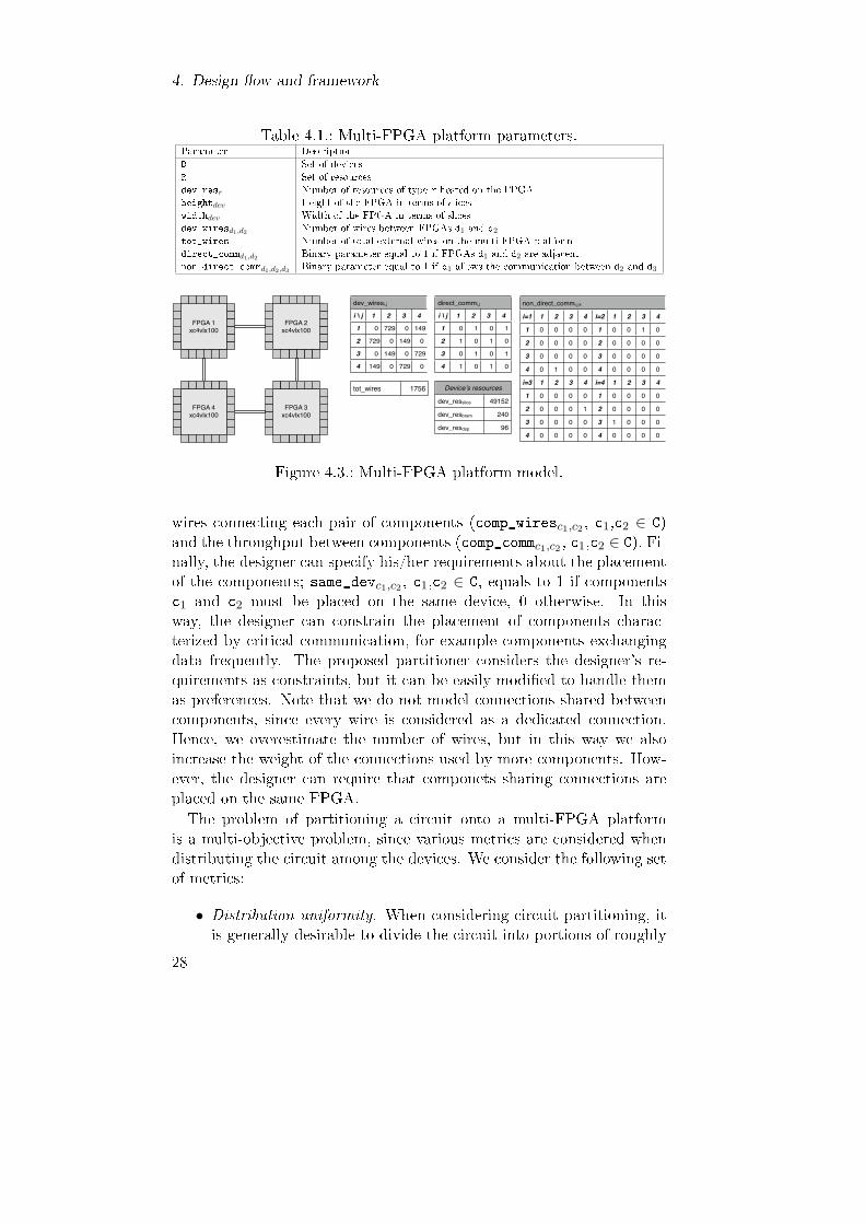
4. Design �ow and framework
Table 4.1.: Multi-FPGA platform parameters.Parameter DescriptionD Set of devicesR Set of resourcesdev_resr Number of resources of type r hosted on the FPGAheightdev Height of the FPGA in terms of sliceswidthdev Width of the FPGA in terms of slicesdev_wiresd1,d2 Number of wires between FPGAs d1 and d2
tot_wires Number of total external wires on the multi-FPGA platformdirect_commd1,d2 Binary parameter equal to 1 if FPGAs d1 and d2 are adjacentnon_direct_commd1,d2,d3 Binary parameter equal to 1 if d1 allows the communication between d2 and d3
FPGA 1xc4vlx100
FPGA 2xc4vlx100
FPGA 4xc4vlx100
FPGA 3xc4vlx100
Deviceʼs resources
dev_resslice 49152
dev_resbram 240
dev_resdsp 96
tot_wires 1756
non_direct_commi,j,k
i=1 1 2 3 4 i=2 1 2 3 4
1 0 0 0 0 1 0 0 1 0
2 0 0 0 0 2 0 0 0 0
3 0 0 0 0 3 0 0 0 0
4 0 1 0 0 4 0 0 0 0
i=3 1 2 3 4 i=4 1 2 3 4
1 0 0 0 0 1 0 0 0 0
2 0 0 0 1 2 0 0 0 0
3 0 0 0 0 3 1 0 0 0
4 0 0 0 0 4 0 0 0 0
dev_wiresi,j
i \ j 1 2 3 4
1 0 729 0 149
2 729 0 149 0
3 0 149 0 729
4 149 0 729 0
direct_commi,j
i \ j 1 2 3 4
1 0 1 0 1
2 1 0 1 0
3 0 1 0 1
4 1 0 1 0
Figure 4.3.: Multi-FPGA platform model.
wires connecting each pair of components (comp_wiresc1,c2 , c1,c2 ∈ C)and the throughput between components (comp_commc1,c2 , c1,c2 ∈ C). Fi-nally, the designer can specify his/her requirements about the placementof the components; same_devc1,c2 , c1,c2 ∈ C, equals to 1 if componentsc1 and c2 must be placed on the same device, 0 otherwise. In thisway, the designer can constrain the placement of components charac-terized by critical communication, for example components exchangingdata frequently. The proposed partitioner considers the designer's re-quirements as constraints, but it can be easily modi�ed to handle themas preferences. Note that we do not model connections shared betweencomponents, since every wire is considered as a dedicated connection.Hence, we overestimate the number of wires, but in this way we alsoincrease the weight of the connections used by more components. How-ever, the designer can require that componets sharing connections areplaced on the same FPGA.The problem of partitioning a circuit onto a multi-FPGA platform
is a multi-objective problem, since various metrics are considered whendistributing the circuit among the devices. We consider the following setof metrics:
• Distribution uniformity. When considering circuit partitioning, itis generally desirable to divide the circuit into portions of roughly
28
4.3. Preliminary partitioning
equal sizes. This is even more important when reliability is takeninto account, to have balanced ratio between used and spare fabric.
• Number of external wires. The number of inter-FPGA connectionsmust be minimized both for the performance degradation with re-spect to intra-FPGA wires and for the limited number of I/O pinsreserved for inter-FPGA communication.
• External communication. For the performance degradation char-acterizing inter-FPGA connections, components with highest com-munication requirements should be placed on the same device.
The output of the partitioning problem is a mapping, specifying foreach component its hosting on one of the devices. This is modeled bythe decision variable xc,d, that equals to 1 if component c is hosted ondevice d, 0 otherwise. Furthermore, to account for communication, weintroduce the binary variables yc1,d1,c2,d2, equal to 1 if component c1 ishosted on device d1 and component c2 is hosted on device d2.The partitioning problem includes constraints associated with compo-
nents placement, system distribution, external wires, and external com-munication, listed in Table 4.5.Components placement constraints. The partitioner must place each
component on a device, as de�ned by Constraint C1. Moreover, the de-signer's requirements related to the placement of componets on the samedevice must be ful�lled. Constraint C5 allows to meet these requirementsby exploiting the variables yc1,d1,c2,d2, that identify the placement of eachcouple of components. Constraints C2, C3, and C4 de�ne the valid valuesof the variables yc1,d1,c2,d2, by referring to the variables xc,d; ConstraintsC2 and C3 de�ne the minimum bound of yc1,d1,c2,d2 (if xc1,d1 or xc2,d2
equal to 0, then yc1,d1,c2,d2 equals to 0), whereas Constraint C4 identi�esthe maximum one (if both xc1,d1 and xc2,d2 equal to 1, then yc1,d1,c2,d2
equals to 1).System distribution constraints. The system must be distributed uni-
formly among the available devices. The resources occupation on eachdevice, computed as the sum of the resources required by the Recon�g-uration Controller and the components hosted on the device, as de�nedby Constraint C6, can not be greater than the available resources, asconstrained by C7. The distribution of the system among the availabledevices is uniform when the gap between the maximum and minimumresources occupations among the devices is null. The maximum andminimum occupations of each type of resources are constrained by C8and C9, and the di�erence between them de�nes the gap, as computedby Constraint C10.
29
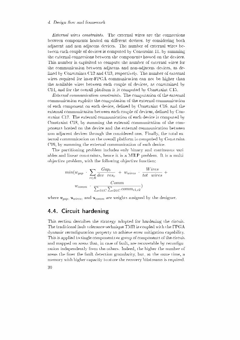
4. Design �ow and framework
External wires constraints. The external wires are the connectionsbetween components hosted on di�erent devices, by considering bothadjacent and non adjacent devices. The number of external wires be-tween each couple of devices is computed by Constraint 11, by summingthe external connections between the components hosted on the devices.This number is exploited to compute the number of external wires forthe communication between adjacent and non-adjacent devices, as de-�ned by Constraints C12 and C13, respectively. The number of externalwires required for inter-FPGA communication can not be higher thanthe available wires between each couple of devices, as constrained byC14, and for the overall platform it is computed by Constraint C15.External communication constraints. The computation of the external
communication exploits the computation of the external communicationof each component on each device, de�ned by Constraint C16, and theexternal communication between each couple of devices, de�ned by Con-straint C17. The external communication of each device is computed byConstraint C18, by summing the external communication of the com-ponents hosted on the device and the external communication betweennon-adjacent devices through the considered one. Finally, the total ex-ternal communication on the overall platform is computed by ConstraintC19, by summing the external communication of each device.The partitioning problem includes only binary and continuous vari-
ables and linear constraints, hence it is a MILP problem. It is a multi-objective problem, with the following objective function:
min(wgap ·∑r∈R
Gapr
dev_resr+ wwires · Wires
tot_wires+
wcomm · Comm∑c1∈C
∑c2∈C commc1,c2
)
where wgap, wwires, and wcomm are weights assigned by the designer.
4.4. Circuit hardening
This section describes the strategy adopted for hardening the circuit.The traditional fault tolerance technique TMR is coupled with the FPGAdynamic recon�guration property to achieve error mitigation capability.This is applied to single components or group of components of the circuitand mapped on areas that, in case of fault, are recoverable by recon�gu-ration independently from the others. Indeed, the higher the number ofareas the �ner the fault detection granularity, but, at the same time, amemory with higher capacity to store the recovery bitstreams is required.
30
4.4. Circuit hardening
Table 4.2.: Preliminary partitioner constraints.
Components placement
C1∑
d∈D xc,d = 1,∀c ∈ C
C2 yc1,d1,c2,d2 ≤ xc1,d1,∀c1, c2 ∈ C, d1, d2 ∈ D
C3 yc1,d1,c2,d2 ≤ xc2,d2,∀c1, c2 ∈ C, d1, d2 ∈ D
C4 yc1,d1,c2,d2 ≥ xc1,d1 + xc2,d2 − 1,∀c1, c2 ∈ C, d1, d2 ∈ D
C5∑
d∈D yc1,d,c2,d ≥ same_devc1,c2,∀c1, c2 ∈ C
System distribution
C6 dev_occupationd,r =∑
c∈C compc,r · xc,d + recr,∀d ∈ D,∀r ∈ R
C7 dev_occupationd,r ≤ dev_resd,r,∀d ∈ D,∀r ∈ R
C8 max_dev_occupationr ≥ dev_occupationd,r,∀d ∈ D,∀r ∈ R
C9 min_dev_occupationr ≤ dev_occupationd,r,∀d ∈ D,∀r ∈ R
C10 Gapr = max_dev_occupationr −min_dev_occupationr,∀r ∈ R
External wires
C11 d_to_d_wiresd1,d2 =∑
c1∈C
∑c2∈C comp_wiresc1,c2 · yc1,d1,c2,d2,∀d1, d2 ∈ D
C12 dev_dir_wiresd1,d2 = d_to_d_wiresd1,d2 · direct_commd1,d2,∀d1, d2 ∈ D
C13 dev_non_dir_wiresd1,d2 =∑d∈D (d_to_d_wiresd1,d · non_direct_commd2,d1,d + d_to_d_wiresd,d2 · non_direct_commd1,d,d2)+∑d3∈D
∑d4∈D d_to_d_wiresd3,d4 · non_direct_commd1,d3,d4 · non_direct_commd2,d3,d4,∀d1, d2 ∈ D
C14 dev_dir_wiresd1,d2 + dev_dir_wiresd2,d1 + dev_non_dir_wiresd1,d2+
dev_non_dir_wiresd2,d1 ≤ dev_wiresd1,d2,∀d1, d2 ∈ D
C15 Wires =∑
d1∈D
∑d2∈D dev_dir_wiresd1,d2 + dev_non_dir_wiresd1,d2
External communication
C16 ext_comp_commc,d =∑
c1∈C comp_commc,c1 · xc,d − comp_commc,c1 · yc,d,c1,d,∀c ∈ C,∀d ∈ D
C17 dev_to_dev_commd1,d2 =∑
c1∈C
∑c2∈C comp_commc1,c2 · yc1,d1,c2,d2,∀d1, d2 ∈ D
C18 dev_commd =∑
c∈C ext_comp_commc,d +∑
d1∈D
∑d2∈D dev_to_dev_commd1,d2 · non_direct_commd,d1,d2,∀d ∈ D
C19 Comm =∑
d∈D dev_commd
The circuit hardening task de�nes the independently recoverable areastaking into account these issues. It performs a design space explorationcomposed of two main activities, described in the following.
4.4.1. Recovery strategy de�nition
The �rst activity performed when hardening the circuit de�nes the pa-rameters constraining the de�nition of the independently recoverable ar-eas on the FPGAs. Such parameters are related to the adopted recoverystrategy, described in the following.When recon�guring to cope with non-recoverable faults, a new con-
�guration that replaces the faulty region in the FPGA with a spare oneis loaded. The strategies for de�ning the recovery con�gurations can beclassi�ed into two categories:
• On-line bitstream computation, that dynamically creates the recov-ery con�gurations, as in [26] and [27], and
• O�-line bitstream computation, that creates the alternative con�g-urations during the design phase, as in [28] and [29].
31
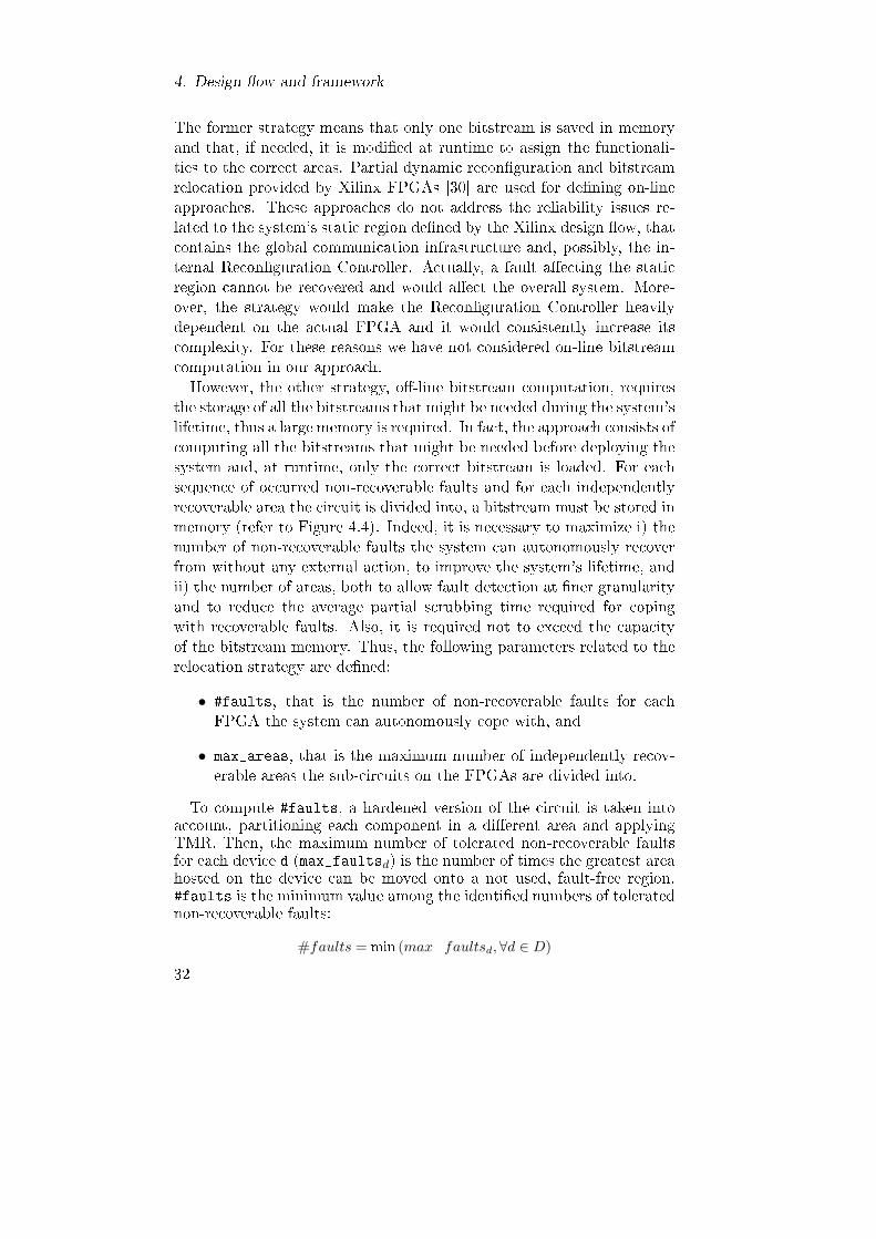
4. Design �ow and framework
The former strategy means that only one bitstream is saved in memoryand that, if needed, it is modi�ed at runtime to assign the functionali-ties to the correct areas. Partial dynamic recon�guration and bitstreamrelocation provided by Xilinx FPGAs [30] are used for de�ning on-lineapproaches. These approaches do not address the reliability issues re-lated to the system's static region de�ned by the Xilinx design �ow, thatcontains the global communication infrastructure and, possibly, the in-ternal Recon�guration Controller. Actually, a fault a�ecting the staticregion cannot be recovered and would a�ect the overall system. More-over, the strategy would make the Recon�guration Controller heavilydependent on the actual FPGA and it would consistently increase itscomplexity. For these reasons we have not considered on-line bitstreamcomputation in our approach.However, the other strategy, o�-line bitstream computation, requires
the storage of all the bitstreams that might be needed during the system'slifetime, thus a large memory is required. In fact, the approach consists ofcomputing all the bitstreams that might be needed before deploying thesystem and, at runtime, only the correct bitstream is loaded. For eachsequence of occurred non-recoverable faults and for each independentlyrecoverable area the circuit is divided into, a bitstream must be stored inmemory (refer to Figure 4.4). Indeed, it is necessary to maximize i) thenumber of non-recoverable faults the system can autonomously recoverfrom without any external action, to improve the system's lifetime, andii) the number of areas, both to allow fault detection at �ner granularityand to reduce the average partial scrubbing time required for copingwith recoverable faults. Also, it is required not to exceed the capacityof the bitstream memory. Thus, the following parameters related to therelocation strategy are de�ned:
• #faults, that is the number of non-recoverable faults for eachFPGA the system can autonomously cope with, and
• max_areas, that is the maximum number of independently recov-erable areas the sub-circuits on the FPGAs are divided into.
To compute #faults, a hardened version of the circuit is taken intoaccount, partitioning each component in a di�erent area and applyingTMR. Then, the maximum number of tolerated non-recoverable faultsfor each device d (max_faultsd) is the number of times the greatest areahosted on the device can be moved onto a not used, fault-free region.#faults is the minimum value among the identi�ed numbers of toleratednon-recoverable faults:
#faults = min (max_faultsd,∀d ∈ D)
32
4.4. Circuit hardening
area 2
area 3 ar
ea 1
area 3ar
ea 1
area 2
area 3ar
ea 1
area 2
area 2
area 3 ar
ea 1
area 3ar
ea 1
area 2
area 3
area
1
area 2
area 3ar
ea 1
area 2
spare region
Initial implementation
Non-recoverable fault in area 2Non-recoverable fault in area 1 Non-recoverable fault in area 3
Non-recoverable fault in area 2 Non-recoverable fault in area 3Non-recoverable fault in area 1 ... ...
Figure 4.4.: The adopted recovery strategy for non-recoverable faults.
When considering multiple subsequent non-recoverable faults, a spe-ci�c bitstream is required for each sequence of occurred faults. Therefore,assuming a given number of independently recoverable areas #areasd,equal to the number of components hosted on FPGA d, to tolerate#faults the following number of alternative bitstreams for each devicehas to be generated:
#bitstreamsd =#faults∑
i=0
#areasid,∀d ∈ D
It is worth noting that #bitstreamsd can be very high also for lowvalues of #faults, hence too a large memory should be required. Thus,the number of areas max_areas is set by ful�lling the memory constraint:
max_areas = max
(#areas |
#faults∑i=0
#areasi ≤ memory_size
bitstream_size
)
being memory_size and bitstream_size the size of the memory and ofthe bitstream for the selected device, respectively. max_areas is consid-ered when de�ning the independently recoverable areas, as described inthe following.
33
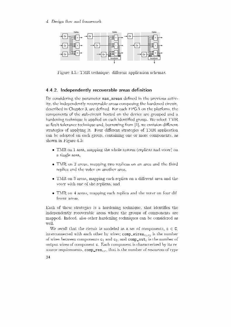
4. Design �ow and framework
TMRa
Gr
Gr
Gr
V
V
V
TMRb
Gr
Gr
Gr
V
V
V
TMRc
Gr
Gr
Gr
V
V
V
localizer localizer
Figure 4.5.: TMR technique: di�erent application schemas.
4.4.2. Independently recoverable areas de�nition
By considering the parameter max_areas de�ned in the previous activ-ity, the independently recoverable areas composing the hardened circuit,described in Chapter 3, are de�ned. For each FPGA on the platform, thecomponents of the sub-circuit hosted on the device are grouped and ahardening technique is applied on each identi�ed group. We select TMRas fault tolerance technique and, borrowing from [1], we envision di�erentstrategies of applying it. Four di�erent strategies of TMR applicationcan be adopted on each group, containing one or more components, asshown in Figure 4.5:
• TMR on 1 area, mapping the whole system (replicas and voter) ona single area,
• TMR on 2 areas, mapping two replicas on an area and the thirdreplica and the voter on another area,
• TMR on 3 areas, mapping each replica on a di�erent area and thevoter with one of the replicas, and
• TMR on 4 areas, mapping each replica and the voter on four dif-ferent areas.
Each of these strategies is a hardening technique, that identi�es theindependently recoverable areas where the groups of components aremapped. Indeed, also other hardening techniques can be considered aswell.We recall that the circuit is modeled as a set of components, c ∈ C,
interconnected with each other by wires; comp_wiresc1,c2 is the numberof wires between components c1 and c2, and comp_outc is the number ofoutput wires of component c. Each component is characterized by its re-source requirements, comp_resc,r, that is the number of resources of type
34
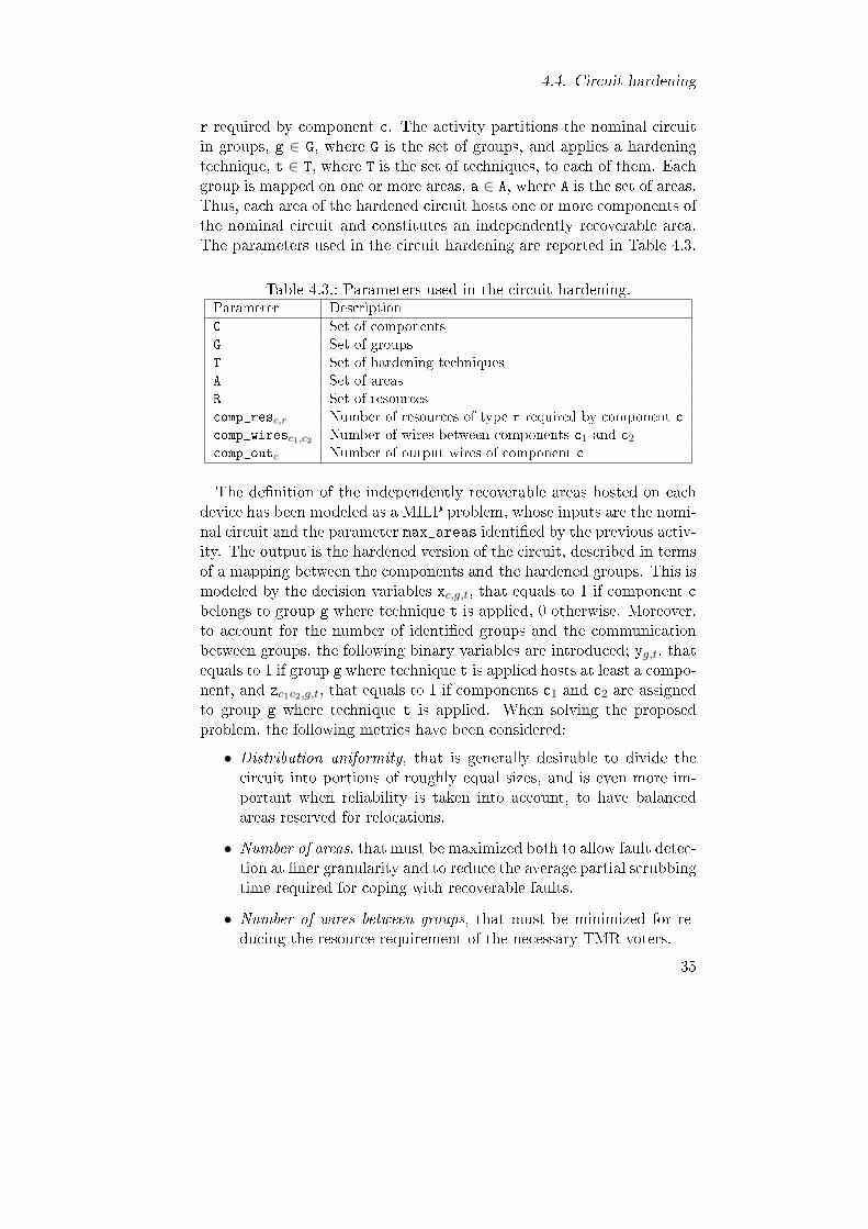
4.4. Circuit hardening
r required by component c. The activity partitions the nominal circuitin groups, g ∈ G, where G is the set of groups, and applies a hardeningtechnique, t ∈ T, where T is the set of techniques, to each of them. Eachgroup is mapped on one or more areas, a ∈ A, where A is the set of areas.Thus, each area of the hardened circuit hosts one or more components ofthe nominal circuit and constitutes an independently recoverable area.The parameters used in the circuit hardening are reported in Table 4.3.
Table 4.3.: Parameters used in the circuit hardening.Parameter DescriptionC Set of componentsG Set of groupsT Set of hardening techniquesA Set of areasR Set of resourcescomp_resc,r Number of resources of type r required by component ccomp_wiresc1,c2 Number of wires between components c1 and c2
comp_outc Number of output wires of component c
The de�nition of the independently recoverable areas hosted on eachdevice has been modeled as a MILP problem, whose inputs are the nomi-nal circuit and the parameter max_areas identi�ed by the previous activ-ity. The output is the hardened version of the circuit, described in termsof a mapping between the components and the hardened groups. This ismodeled by the decision variables xc,g,t, that equals to 1 if component cbelongs to group g where technique t is applied, 0 otherwise. Moreover,to account for the number of identi�ed groups and the communicationbetween groups, the following binary variables are introduced; yg,t, thatequals to 1 if group g where technique t is applied hosts at least a compo-nent, and zc1c2,g,t, that equals to 1 if components c1 and c2 are assignedto group g where technique t is applied. When solving the proposedproblem, the following metrics have been considered:
• Distribution uniformity, that is generally desirable to divide thecircuit into portions of roughly equal sizes, and is even more im-portant when reliability is taken into account, to have balancedareas reserved for relocations.
• Number of areas, that must be maximized both to allow fault detec-tion at �ner granularity and to reduce the average partial scrubbingtime required for coping with recoverable faults.
• Number of wires between groups, that must be minimized for re-ducing the resource requirement of the necessary TMR voters.
35

4. Design �ow and framework
The problem of hardening the nominal circuit and partitioning itin independently recoverable areas includes constraints associated withgroups de�nition, wires between groups, and resources distribution, listedin Table 4.5.Groups de�nition constraints. The hardening process must assign each
component to a group, as de�ned by Constraint C1. Moreover, eachgroup hosting at least a component must be hardened by means of atechnique. Constraint C4 allows to meet this requirement by exploitingthe variables yg,t, that identify the groups hosting at least a compo-nent. Constraints C2 and C3 de�ne the valid values of the variables yg,t,by identifying the maximum bound and the minimum one, respectively.Finally, the number of areas allocated for mapping the groups cannotbe higher than max_areas, required by the relocation strategy, or lowerthan min_areas, possibly used to constrain the fault detection granular-ity, as de�ned by Constraints C6 and C7, respectively. Constraint C5computes the number of allocated areas by taking into account the num-ber of groups and the number of areas required by the applied technique(#areas_reqt).Wires between groups constraints. The number of connections between
groups is identi�ed by computing the number of wires between compo-nents hosted on di�erent groups, as de�ned by Constraint C11. Thevariables zc1,c2,g,t are exploited. Constraints C8 - C10 de�ne the validvalues of the variables zc1,c2,g,t, by identifying the maximum bound (Con-straints C8 and C9) and the minimum one (Constraint C10).Resources distribution constraints. The resource requirement of each
area is computed by considering the occupation of the components hostedon it and the occupation of the voter, as de�ned by Constraint C12. Tocompute the occupation of the components hosted on the area, the pa-rameters w_compt,a,r are exploited, de�ning the number of componentsrequired by the applied technique on the area. To compute the occupa-tion of the voter, depending on the number of voted wires, the parametersw_votert,a,r are exploited, indicating the multiplication factor for wires.Indeed, the resource requirements of the areas can not exceed the re-source availability on the FPGA, as de�ned by Constraint C13. Whendedicated resources (e.g., BRAMs, DSPs) are not su�cient, it is possibleto convert them in slices; such conversion is made for all the replicas of amodule to have areas characterized by uniform distribution. ConstraintsC14 and C15 identify the area with the minimum resource requirementand the area with the maximum one, respectively. It is worth notinghow the area with the minimum resource requirement is de�ned by con-sidering only the areas hosting components; we exploit the parameter M,a enough big value that allows to avoid wrong values of minr when con-
36
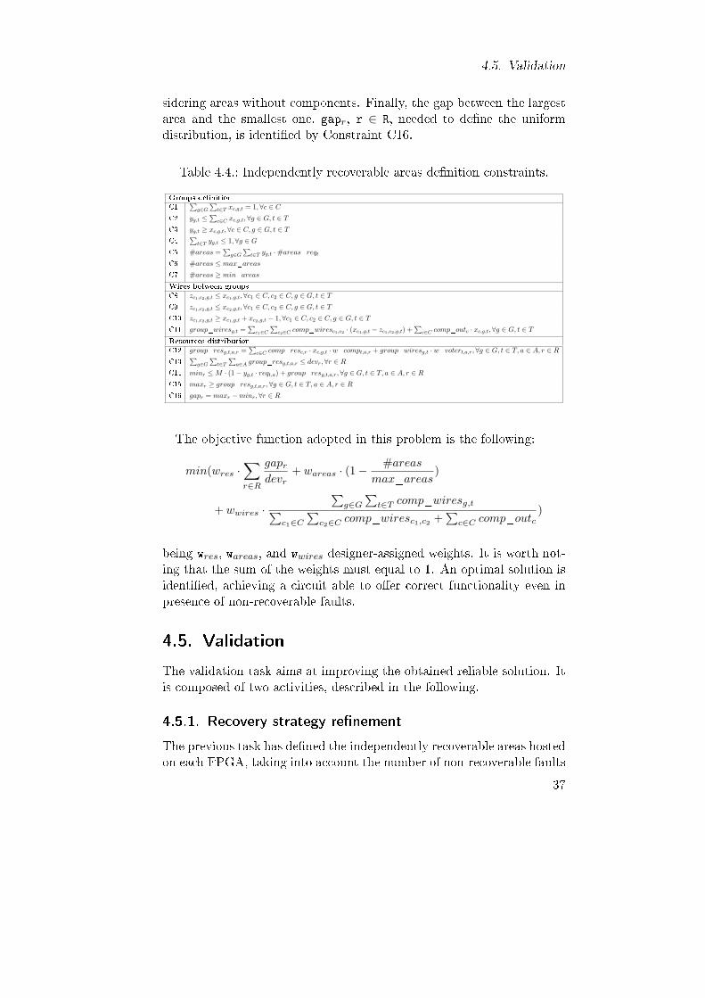
4.5. Validation
sidering areas without components. Finally, the gap between the largestarea and the smallest one, gapr, r ∈ R, needed to de�ne the uniformdistribution, is identi�ed by Constraint C16.
Table 4.4.: Independently recoverable areas de�nition constraints.
Groups de�nition
C1∑
g∈G
∑t∈T xc,g,t = 1,∀c ∈ C
C2 yg,t ≤∑
c∈C xc,g,t,∀g ∈ G, t ∈ T
C3 yg,t ≥ xc,g,t,∀c ∈ C, g ∈ G, t ∈ T
C4∑
t∈T yg,t ≤ 1,∀g ∈ G
C5 #areas =∑
g∈G
∑t∈T yg,t ·#areas_reqt
C6 #areas ≤ max_areas
C7 #areas ≥ min_areas
Wires between groups
C8 zc1,c2,g,t ≤ xc1,g,t,∀c1 ∈ C, c2 ∈ C, g ∈ G, t ∈ T
C9 zc1,c2,g,t ≤ xc2,g,t,∀c1 ∈ C, c2 ∈ C, g ∈ G, t ∈ T
C10 zc1,c2,g,t ≥ xc1,g,t + xc2,g,t − 1,∀c1 ∈ C, c2 ∈ C, g ∈ G, t ∈ T
C11 group_wiresg,t =∑
c1∈C
∑c2∈C comp_wiresc1,c2 · (xc1,g,t − zc1,c2,g,t) +
∑c∈C comp_outc · xc,g,t,∀g ∈ G, t ∈ T
Resources distribution
C12 group_resg,t,a,r =∑
c∈C comp_resc,r · xc,g,t · w_compt,a,r + group_wiresg,t · w_votert,a,r,∀g ∈ G, t ∈ T, a ∈ A, r ∈ R
C13∑
g∈G
∑t∈T
∑a∈A group_resg,t,a,r ≤ devr,∀r ∈ R
C14 minr ≤ M · (1− yg,t · reqt,a) + group_resg,t,a,r,∀g ∈ G, t ∈ T, a ∈ A, r ∈ R
C15 maxr ≥ group_resg,t,a,r,∀g ∈ G, t ∈ T, a ∈ A, r ∈ R
C16 gapr = maxr −minr,∀r ∈ R
The objective function adopted in this problem is the following:
min(wres ·∑r∈R
gapr
devr+ wareas · (1−
#areas
max_areas)
+ wwires ·∑
g∈G
∑t∈T comp_wiresg,t∑
c1∈C
∑c2∈C comp_wiresc1,c2 +
∑c∈C comp_outc
)
being wres, wareas, and wwires designer-assigned weights. It is worth not-ing that the sum of the weights must equal to 1. An optimal solution isidenti�ed, achieving a circuit able to o�er correct functionality even inpresence of non-recoverable faults.
4.5. Validation
The validation task aims at improving the obtained reliable solution. Itis composed of two activities, described in the following.
4.5.1. Recovery strategy re�nement
The previous task has de�ned the independently recoverable areas hostedon each FPGA, taking into account the number of non-recoverable faults
37

4. Design �ow and framework
tolerated on each device (#faults). Indeed, #faults is a preliminaryestimate, evaluated by considering a hardening of the sub-circuits atcomponent level. The recovery strategy re�nement activity re-evaluatesthe number of tolerated non-recoverable faults, by taking into accountthe hardened circuit de�ned by the previous activity.For each FPGA d, the maximum number of tolerated non-recoverable
faults (max_faultsd) is computed by considering the number of timesthe greatest independently recoverable area hosted on the device canbe relocated on the spare region. Then, the constraint imposed by thememory capacity is taken into account and the actual number of non-recoverable faults tolerated by the system on each FPGA is de�ned asfollows:
#faults = min
(#faultsd |
#faultsd∑i=0
#areasid ≤
memory_size
bitstream_size,∀d ∈ D
)
where #areasd is the number of independently recoverable areas hostedon FPGA d and #faultsd ≤ max_faultsd is the tolerated number offaults.This value is considered by the subsequent reliability-aware partition-
ing activity, that re-distributes the circuit among the available FPGAs,also taking into account the recovery actions.
4.5.2. Reliability-aware partitioning
The independently recoverable areas de�ned in the previous task aretaken in input by the reliability-aware partitioning task, that distributesthem among the available FPGAs, with the aim of possibly improvingthe obtained solution. The reliability-aware partitioner is an extensionof the one presented in Section 4.3, considering also the possible recoveryactions needed during the system's lifetime.In literature, the problem of partitioning hardware circuits has been
widely investigated and various approaches have been proposed. Somecontributions [31, 32, 33] partition design speci�cations at the behav-ioral level, providing limited details about the systems' implementation,which for FPGA platforms are quite relevant. Other approaches [34, 35]take into account only the routing between FPGAs, without consideringthe structure of the recon�gurable fabric, peculiar and heterogeneous inthe most recent FPGA families. Therefore, those works adopting eithera simpli�ed homogeneous model of the resources (e.g., [36, 37, 38]) or aheterogeneous one but with a uniform distribution (e.g., [39]) can onlybe used in speci�c application scenarios, since with the detailed modelof up-to-date devices would be inaccurate and would possibly lead to
38

4.5. Validation
unfeasible solutions. Finally, some contributions seek a cover of the cir-cuit in terms of used devices (e.g., [40, 41, 42, 43, 44, 45, 46]), howeverthese approaches do not model the platform's topology. Again, the ap-proaches proposed in literature could be used as hints for a preliminaryexploration of the solution space, but not as �nal methods to be intro-duced within an automatic design �ow, which should always produces afeasible solution. Moreover, none of the approaches actually deals withthe speci�cs of hardened systems, which have additional requirements interms of resources and placement. Finally, while most of the contribu-tions in literature present algorithms based on heuristics, we propose aMILP model that identi�es the global optimal solution in an acceptableexecution time. It is worth noting that, even if the approach has beendesigned to handle hardened systems, it is possible to use it also fornominal systems, with no fault management features.The partitioner takes as input the independently recoverable areas
composing the reliable circuit. Each area is characterized by its resourcerequirements, areaa,r, a ∈ A, r ∈ R, that is the number of resourcesof type r required by area a. The communication between the areasis modeled by specifying the number of wires connecting each pair ofareas (areas_wiresa1,a2 , a1,a2 ∈ A) and the throughput between areas(areas_comma1,a2 , a1,a2 ∈ A). Finally, the designer can specify his/herrequirements about the placement of the areas; same_deva1,a2 , a1,a2 ∈A, equals to 1 if areas a1 and a2 must be placed on the same device, 0otherwise.When distributing the reliable circuit among the devices, the same
set of metrics of the preliminary partitioner are considered, namely thedistribution uniformity, the number of external wires, and the externalcommunication. The output of the partitioning problem is a mapping,specifying for each area its hosting on one of the devices (it will be the�oorplanner, in the subsequent step, to position it inside the device).This is modeled by the decision variable xa,d, that equals to 1 if area a ishosted on device d, 0 otherwise. Furthermore, to account for communi-cation and the spare areas, the following binary variables are introduced:
• ya1,d1,a2,d2, equals to 1 if area a1 is hosted on device d1 and areaa2 is hosted on device d2;
• za,r,d, equals to 1 if area a requires the maximum number of re-sources of type r on device d.
The partitioning problem includes constraints associated with areasplacement, system distribution, external wires, and external communi-cation, listed in Table 4.5.
39
4. Design �ow and framework
Areas placement constraints. The partitioner must place each area ona device, as de�ned by Constraint C1. Moreover, the designer's require-ments related to the placement of areas on the same device must beful�lled. Constraint C5 allows to meet these requirements by exploitingthe variables ya1,d1,a2,d2, that identify the placement of each couple of ar-eas. Constraints C2, C3, and C4 de�ne the valid values of the variablesya1,d1,a2,d2, by referring to the variables xa,d; Constraints C2 and C3 de-�ne the minimum bound of ya1,d1,a2,d2 (if xa1,d1 or xa2,d2 equal to 0, thenya1,d1,a2,d2 equals to 0), whereas Constraint C4 identi�es the maximumone (if both xa1,d1 and xa2,d2 equal to 1, then ya1,d1,a2,d2 equals to 1).System distribution constraints. The system must be distributed uni-
formly among the available devices, by considering both the areas hostingthe system components and the spare ones. The spare area(s) must in-clude enough resources to host the greatest area among the ones placedon the device. Constraints C6 and C7 de�ne the variables za,r,d, neces-sary to identify the greatest area for each type of resources on each device;Constraint C6 de�nes that za,r,d equals to 0 if the area is not hosted onthe device, and Constraint C7 de�nes that there is one greatest area foreach type of resources on each device. The spare area is identi�ed byConstraints C8 and C9; Constraint C8 de�nes that the spare area mustcontain enough resources for relocating every area hosted on the device,and Constraint C9 sets the resources requirements of the spare area toequal the ones of the greatest area on the device for each type of re-sources. A number of spare areas equal to the number of non-recoverablefaults speci�ed by the designer must be reserved on each device. Thespare areas concur in the computation of the resources occupation, to-gether with the resources required by the Recon�guration Controller andthe areas hosted on the device, as computed by Constraint C10. The re-sources occupation on each device can not be greater than the availableresources, as constrained by C11. The distribution of the system amongthe available devices is uniform when the gap between the maximum andminimum resources occupations among the devices is null. The maxi-mum and minimum occupations of each type of resources are constrainedby C12 and C13, and the di�erence between them de�nes the gap, ascomputed by Constraint C14.External wires constraints. The external wires are the connections
between areas hosted on di�erent devices, by considering both adjacentand non adjacent devices. The number of external wires between eachcouple of devices is computed by Constraint 15, by summing the externalconnections between the areas hosted on the devices. This number isexploited to compute the number of external wires for the communicationbetween adjacent and non-adjacent devices, as de�ned by Constraints
40

4.5. Validation
Table 4.5.: Reliability-aware partitioner constraints.
Areas placement
C1∑
d∈D xa,d = 1,∀a ∈ A
C2 ya1,d1,a2,d2 ≤ xa1,d1,∀a1, a2 ∈ A, d1, d2 ∈ D
C3 ya1,d1,a2,d2 ≤ xa2,d2,∀a1, a2 ∈ A, d1, d2 ∈ D
C4 ya1,d1,a2,d2 ≥ xa1,d1 + xa2,d2 − 1,∀a1, a2 ∈ A, d1, d2 ∈ D
C5∑
d∈D ya1,d,a2,d ≥ same_deva1,a2,∀a1, a2 ∈ A
System distribution
C6 za,r,d ≤ xa,d,∀a ∈ A,∀r ∈ R,∀d ∈ D
C7∑
a∈A za,r,d ≤ 1,∀r ∈ R,∀d ∈ D
C8 spare_resd,r ≥ areaa,r · xa,d,∀d ∈ D,∀r ∈ R,∀a ∈ A
C9 spare_resd,r =∑
a∈A areaa,r · za,r,d,∀d ∈ D,∀r ∈ R
C10 dev_occupationd,r =∑
a∈A areaa,r · xa,d + recr + max_faults · spare_resd,r,∀d ∈ D,∀r ∈ R
C11 dev_occupationd,r ≤ dev_resd,r,∀d ∈ D,∀r ∈ R
C12 max_dev_occupationr ≥ dev_occupationd,r,∀d ∈ D,∀r ∈ R
C13 min_dev_occupationr ≤ dev_occupationd,r,∀d ∈ D,∀r ∈ R
C14 Gapr = max_dev_occupationr −min_dev_occupationr,∀r ∈ R
External wires
C15 d_to_d_wiresd1,d2 =∑
a1∈A
∑a2∈A areas_wiresa1,a2 · ya1,d1,a2,d2,∀d1, d2 ∈ D
C16 dev_dir_wiresd1,d2 = d_to_d_wiresd1,d2 · direct_commd1,d2,∀d1, d2 ∈ D
C17 dev_non_dir_wiresd1,d2 =∑d∈D (d_to_d_wiresd1,d · non_direct_commd2,d1,d + d_to_d_wiresd,d2 · non_direct_commd1,d,d2)+∑d3∈D
∑d4∈D d_to_d_wiresd3,d4 · non_direct_commd1,d3,d4 · non_direct_commd2,d3,d4,∀d1, d2 ∈ D
C18 dev_dir_wiresd1,d2 + dev_dir_wiresd2,d1 + dev_non_dir_wiresd1,d2+
dev_non_dir_wiresd2,d1 ≤ dev_wiresd1,d2,∀d1, d2 ∈ D
C19 Wires =∑
d1∈D
∑d2∈D dev_dir_wiresd1,d2 + dev_non_dir_wiresd1,d2
External communication
C20 ext_area_comma,d =∑
a1∈A areas_comma,a1 · xa,d − area_comma,a1 · ya,d,a1,d,∀a ∈ A,∀d ∈ D
C21 dev_to_dev_commd1,d2 =∑
a1∈A
∑a2∈A areas_comma1,a2 · ya1,d1,a2,d2,∀d1, d2 ∈ D
C22 dev_commd =∑
a∈A ext_area_comma,d +∑
d1∈D
∑d2∈D dev_to_dev_commd1,d2 · non_direct_commd,d1,d2,∀d ∈ D
C23 Comm =∑
d∈D dev_commd
C16 and C17, respectively. The number of external wires required forinter-FPGA communication can not be higher than the available wiresbetween each couple of devices, as constrained by C18, and for the overallplatform it is computed by Constraint C19.External communication constraints. The computation of the external
communication exploits the computation of the external communicationof each area on each device, de�ned by Constraint C20, and the externalcommunication between each couple of devices, de�ned by ConstraintC21. The external communication of each device is computed by Con-straint C22, by summing the external communication of the areas hostedon the device and the external communication between non-adjacent de-vices through the considered one. Finally, the total external communica-tion on the overall platform is computed by Constraint C23, by summingthe external communication of each device.The partitioning problem includes only binary and continuous vari-
ables and linear constraints, hence it is a MILP problem. It is a multi-
41

4. Design �ow and framework
objective problem, with the following objective function:
min(wgap ·∑r∈R
Gapr
dev_resr+ wwires · Wires
tot_wires+
wcomm · Comm∑a1∈A
∑a2∈A comma1,a2
)
where wgap, wwires, and wcomm are weights assigned by the designer.
4.6. Floorplanning
The �oorplanning task �nds a suitable placement of the hardened areason the FPGA fabric (refer to Table 4.1 for the parameters character-izing the device). Indeed, also the Recon�guration Controller is con-sidered as an area to be positioned on the device. The areas are seenas rectangles of speci�ed height and width, identi�ed by coordinates [(xBL,yBL),(xTR,yTR) ], being the bottom left corner and the top rightcorner, respectively. To obtain a feasible implementation, they mustsatisfy the following constraints:
• Each area is contained in the device:
0 ≤ xBLa < xTRa < widthdev, ∀a ∈ A
0 ≤ yBLa < yTRa < heightdev, ∀a ∈ A
• Di�erent areas do not overlap with each other:
a1 ∩ a2 = �, ∀a1, a2 ∈ A
• Each area satis�es the resources requirements:
areaa,r ≤ area_resa,r, ∀a ∈ A, ∀r ∈ R
where areaa,r is the number of resources of type r required bycomponents implemented in area a and area_resa,r is the numberof resources of type r contained in area a.
These areas, being recon�gurable, are subject to recon�guration con-straints too. The FPGAs recon�guration capability is exploited by iden-tifying the number of rows of frames (num_frame_rows) and the numberof frames per column for each kind of resource, allowing to accuratelycompute the recon�guration overhead. The distinction between 1D and2D recon�guration is modeled by imposing constraints on the de�nitionof the recon�gurable areas:
42
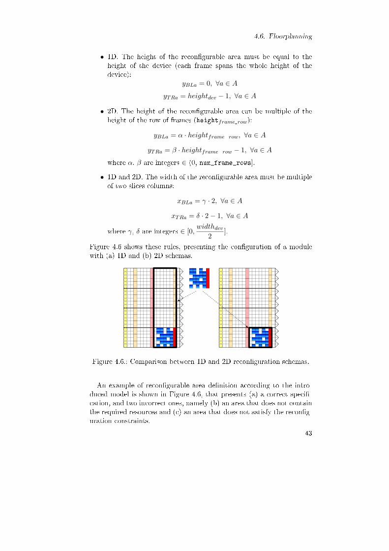
4.6. Floorplanning
• 1D. The height of the recon�gurable area must be equal to theheight of the device (each frame spans the whole height of thedevice):
yBLa = 0, ∀a ∈ A
yTRa = heightdev − 1, ∀a ∈ A
• 2D. The height of the recon�gurable area can be multiple of theheight of the row of frames (heightframe_row):
yBLa = α · heightframe_row, ∀a ∈ A
yTRa = β · heightframe_row − 1, ∀a ∈ A
where α, β are integers ∈ (0, num_frame_rows].
• 1D and 2D. The width of the recon�gurable area must be multipleof two slices columns:
xBLa = γ · 2, ∀a ∈ A
xTRa = δ · 2− 1, ∀a ∈ A
where γ, δ are integers ∈ [0,widthdev
2].
Figure 4.6 shows these rules, presenting the con�guration of a modulewith (a) 1D and (b) 2D schemas.
Figure 4.6.: Comparison between 1D and 2D recon�guration schemas.
An example of recon�gurable area de�nition according to the intro-duced model is shown in Figure 4.6, that presents (a) a correct speci�-cation, and two incorrect ones, namely (b) an area that does not containthe required resources and (c) an area that does not satisfy the recon�g-uration constraints.
43
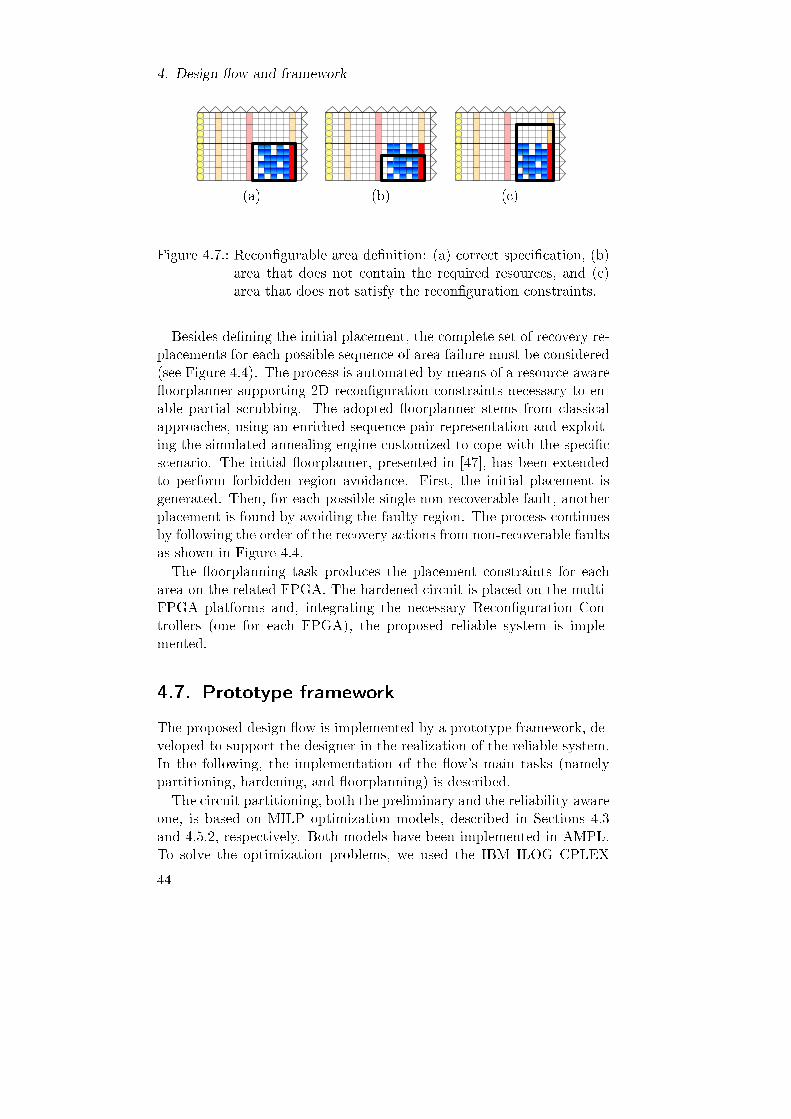
4. Design �ow and framework
(a) (b) (c)
Figure 4.7.: Recon�gurable area de�nition: (a) correct speci�cation, (b)area that does not contain the required resources, and (c)area that does not satisfy the recon�guration constraints.
Besides de�ning the initial placement, the complete set of recovery re-placements for each possible sequence of area failure must be considered(see Figure 4.4). The process is automated by means of a resource-aware�oorplanner supporting 2D recon�guration constraints necessary to en-able partial scrubbing. The adopted �oorplanner stems from classicalapproaches, using an enriched sequence pair representation and exploit-ing the simulated annealing engine customized to cope with the speci�cscenario. The initial �oorplanner, presented in [47], has been extendedto perform forbidden region avoidance. First, the initial placement isgenerated. Then, for each possible single non-recoverable fault, anotherplacement is found by avoiding the faulty region. The process continuesby following the order of the recovery actions from non-recoverable faultsas shown in Figure 4.4.The �oorplanning task produces the placement constraints for each
area on the related FPGA. The hardened circuit is placed on the multi-FPGA platforms and, integrating the necessary Recon�guration Con-trollers (one for each FPGA), the proposed reliable system is imple-mented.
4.7. Prototype framework
The proposed design �ow is implemented by a prototype framework, de-veloped to support the designer in the realization of the reliable system.In the following, the implementation of the �ow's main tasks (namelypartitioning, hardening, and �oorplanning) is described.The circuit partitioning, both the preliminary and the reliability-aware
one, is based on MILP optimization models, described in Sections 4.3and 4.5.2, respectively. Both models have been implemented in AMPL.To solve the optimization problems, we used the IBM ILOG CPLEX
44

4.8. Design �ow for �xed number of non-recoverable faults
12.1 tool, which implements a parallel branch and cut procedure [48].The physical system supporting the partitioner execution is based onVMWare ESXi 4.0, running on an Intel Nehalem dual socket quad-coresystem with 32 GB of RAM. CPLEX is hosted on a Virtual Machine(VM) running Ubuntu 11.04 Linux. The VM has four physical cores ded-icated to its execution with guaranteed performance and 8GB of memoryreserved. The partitioner performance has been measured and evaluatedin terms of execution time, as reported in Appendix A, showing that,despite being the partitioning problem NP-complete [49], the proposedmodels run in acceptable time.The CPLEX tool has been exploited also to solve the optimization
model for the independently recoverable areas de�nition task, describedin Section 4.4. Also this optimization model has been implemented inAMPL.Finally, the �oorplanning task has been developed in a C++ proto-
type. This �oorplanner has been empirically evaluated by means of theexperimental campaign reported in [47].By performing the tasks above, the developed prototype framework
allows to identify the solution o�ering the most convenient trade-o� withrespect to the designer's requirements.
4.8. Design �ow for �xed number of
non-recoverable faults
The design �ow described in the previous sections builds the envisionedfault tolerant system on a multi-FPGA platform speci�ed by the de-signer. Alternatively, it is possible to de�ne the reliable system based onthe number of non-recoverable faults that must be tolerated; after pre-dicting the number of non-recoverable faults expected during the mis-sion lifetime, the minimum number of FPGAs required to implementthe hardened circuit and the Recon�guration Controllers is identi�ed. Adesign �ow targeted at this second scenario is required.The proposed �ow for designing the fault tolerant system when the
number of non-recoverable faults is �xed is shown in Figure 4.8. Withrespect to the previous �ow, the required inputs and the preliminarypartitioning task change. Whereas the previous �ow takes in input themodel of the multi-FPGA platform, this second approach requires themodel of the single FPGAs composing the platform and the numberof non-recoverable faults to be tolerated. The circuit components aretaken in input by the reliability-aware iterative partitioning task, thatdistributes them among the necessary FPGAs. A hardened version of the
45

4. Design �ow and framework
circuit is taken into account, where TMR is applied on each component.By starting from two FPGAs, the partitioner distributes the hardenedcomponents among the devices and increases the number of requiredFPGAs as far as it identi�es the suitable spare region for tolerating thenon-recoverable faults. The subsequent tasks are the ones of the previous�ow. The two approaches are compared in Chapter 7 by implementinga real case study.
VHDLnominal circuit
RELIABILITY-AWARE PARTITIONING
FLOORPLANNING
BITs
device model
circuitmodel
IMPLEMENTATIONVHDLReconfiguration
Controller
reliable circuit
UCFs
mapping area-FPGA
recovery strategy definition
CIRCUIT HARDENING
RELIABILITY-AWARE ITERATIVE PARTITIONING
mapping component-FPGA
independently recoverable areas definition
recovery strategy refinement
SYNTHESIS AND PARSING
VALIDATION# non-rec faults
+
Figure 4.8.: Design �ow for �xed number of non-recoverable faults.
4.9. Chapter summary
In this chapter, we have introduced a �ow for designing fault tolerantsystems according to the methodology proposed in the thesis. A proto-type framework implementing the �ow has been developed, in order toautomate as much as possible the implementation of such systems. Allthe various implementation issues characterizing modern FPGAs havebeen taken into account and an accurate model of the multi-FPGA plat-
46

4.9. Chapter summary
form has been adopted. The proposed design �ow produces a feasiblesolution implementing an autonomous fault tolerant system.
47

5. Fault classi�cation
When FPGAs, in particular SRAM-based ones, are exploited for mission-critical applications, fault tolerance and recovery techniques must be ap-plied, but �rst it is necessary to understand the faults themselves in orderto apply the suitable recovery action. In fact, some faults can be recov-ered by recon�guring the device (and possibly only the faulty part) withthe same con�guration loaded before the fault occurrence, while others,characterized by a destructive e�ect, lead to the necessity of relocatingthe functionality loaded onto the faulty part of the device. This chapterpresents a classi�cation strategy and its companion algorithm for thediscrimination of faults in FPGAs based on their impact on the deviceelements and the consequent possibility to recover from them, so clas-sifying faults into two macro categories; recoverable and non-recoverableones. Once classi�cation has been carried out, the suitable fault recov-ery strategy is applied, with the �nal aim of enabling the exploitation ofSRAM-based FPGAs for mission-critical applications, such as the onesin the space environment. While the idea behind the classi�cation strat-egy is straightforward and intuitive, the de�nition of the parameters atthe basis of such an approach is the real challenge and complex point.The main contributions of our work are thus the formal de�nition ofthe parameters characterizing the algorithm and the evaluation of theconditions for correct fault classi�cation.The chapter is structured as follows: Section 5.1 discusses the related
work. Sections 5.2 and 5.3 describe two preliminary proposals of faultclassi�cation algorithms, presented in [50] and [51], respectively. Sec-tion 5.4 describes the proposed algorithm and Section 5.5 discusses itsevaluation. Finally, Section 5.6 draws the chapter summary.
5.1. Related work
Few works in literature deal with the problem of identifying faults thatphysically damage the device.An approach dealing with the discrimination of faults in FPGAs is
presented in [52]. The authors propose the use of a timer; if two errorsare revealed in the same position in a time interval smaller than a pre-de�ned threshold, it is assumed that they are related to the presence of a
49
5. Fault classi�cation
fault that has physically damaged the device. The main drawback of theapproach is that it is based on the knowledge of the Mean Time BetweenFailure (MTBF), that is highly variable, being dependent on the speci�coperating conditions.The work presented in [53] pursues an objective similar to ours, by
proposing a mechanism for the diagnosis of hard faults in microproces-sors. The approach diagnoses hard faults at the Field Decon�gurableUnit (FDU) level of granularity. When an error is detected in an in-struction executed by the microprocessor, an error counter for every FDUused by that instruction is incremented and, when a counter exceeds athreshold, the related FDU is identi�ed as a�ected by a hard fault, andis decon�gured and no longer used. As long as transient errors do notlead the error counters to exceed the threshold, the counters are clearedperiodically with a frequency depending on the expected transient errorrates, or when a decon�guration is activated. Moreover, the thresholdis chosen not to be too small and is related to the speci�c FDU usage.Although the overall solution is presented, no indication is available onhow to derive the parameters' value.Indeed, we deem fundamental to be able to de�ne the values of the pa-
rameters to distinguish between recoverable and non-recoverable faults,in a systematic way based on the application scenario. Therefore, al-though the existing proposals are meaningful in terms of the presentedstrategies, they cannot be adopted. In particular, we focus our attentionon how to derive such parameters, in a more general way, also determin-ing them for our environmental space-mission context. More precisely,with respect to the previous contributions, the proposed work formallyde�nes the parameters characterizing the algorithm and evaluates theconditions for correct fault classi�cation, presenting a robustness analy-sis, in order to see how the overall behavior may be a�ected by possibleimpreciseness.
5.2. First preliminary proposal
A �rst preliminary proposal of fault classi�cation algorithm has beenpresented in [50]. We propose a classi�cation of the fault a�ecting aportion of the FPGA based on the absolute and relative frequency ofthe detected faults. The rationale is that, if an area is a�ected by afault more frequently than the others, a relocation should take place toprevent further use of the area.The de�ned strategy keeps track of both the number of faults oc-
curring in each area (application areas and controller) and of their his-
50
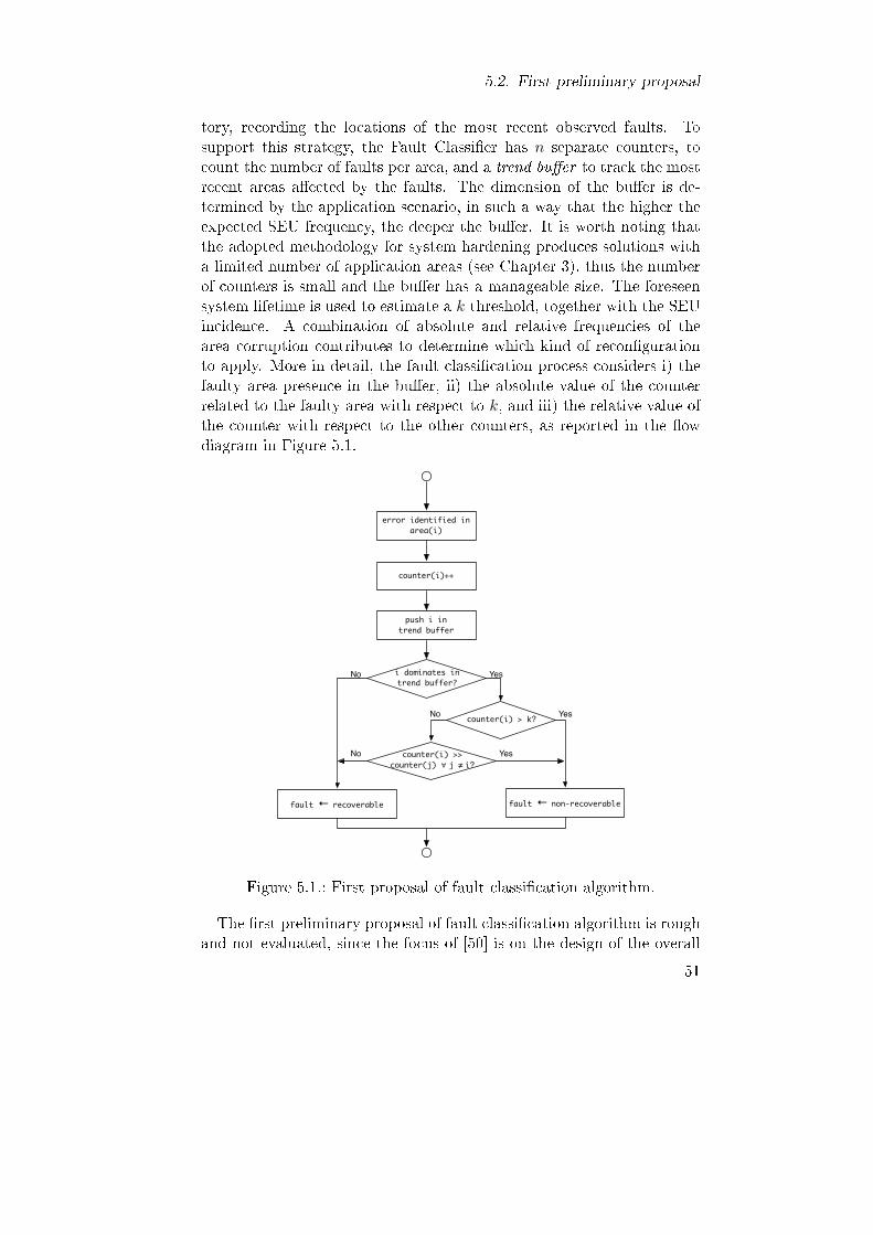
5.2. First preliminary proposal
tory, recording the locations of the most recent observed faults. Tosupport this strategy, the Fault Classi�er has n separate counters, tocount the number of faults per area, and a trend bu�er to track the mostrecent areas a�ected by the faults. The dimension of the bu�er is de-termined by the application scenario, in such a way that the higher theexpected SEU frequency, the deeper the bu�er. It is worth noting thatthe adopted methodology for system hardening produces solutions witha limited number of application areas (see Chapter 3), thus the numberof counters is small and the bu�er has a manageable size. The foreseensystem lifetime is used to estimate a k threshold, together with the SEUincidence. A combination of absolute and relative frequencies of thearea corruption contributes to determine which kind of recon�gurationto apply. More in detail, the fault classi�cation process considers i) thefaulty area presence in the bu�er, ii) the absolute value of the counterrelated to the faulty area with respect to k, and iii) the relative value ofthe counter with respect to the other counters, as reported in the �owdiagram in Figure 5.1.
counter(i)++
push i in trend buffer
i dominates in trend buffer?
counter(i) > k?
counter(i) >> counter(j) ∀ j ≠ i?
No
No
No
Yes
Yes
Yes
error identified in area(i)
fault ← non-recoverablefault ← recoverable
Figure 5.1.: First proposal of fault classi�cation algorithm.
The �rst preliminary proposal of fault classi�cation algorithm is roughand not evaluated, since the focus of [50] is on the design of the overall
51
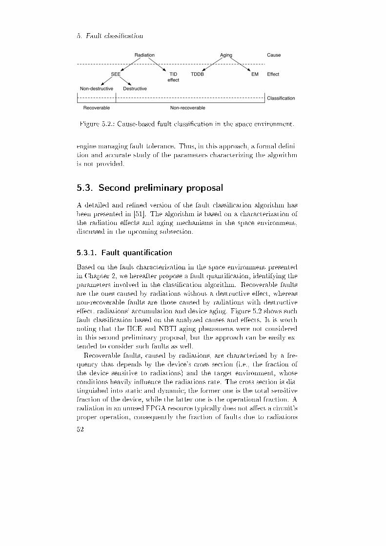
5. Fault classi�cation
Radiation Aging
TIDeffect
EMSEE TDDB
Non-destructive Destructive
Recoverable Non-recoverable
Cause
Effect
Classification
Figure 5.2.: Cause-based fault classi�cation in the space environment.
engine managing fault tolerance. Thus, in this approach, a formal de�ni-tion and accurate study of the parameters characterizing the algorithmis not provided.
5.3. Second preliminary proposal
A detailed and re�ned version of the fault classi�cation algorithm hasbeen presented in [51]. The algorithm is based on a characterization ofthe radiation e�ects and aging mechanisms in the space environment,discussed in the upcoming subsection.
5.3.1. Fault quanti�cation
Based on the fault characterization in the space environment presentedin Chapter 2, we hereafter propose a fault quanti�cation, identifying theparameters involved in the classi�cation algorithm. Recoverable faultsare the ones caused by radiations without a destructive e�ect, whereasnon-recoverable faults are those caused by radiations with destructivee�ect, radiations' accumulation and device aging. Figure 5.2 shows suchfault classi�cation based on the analyzed causes and e�ects. It is worthnoting that the HCE and NBTI aging phenomena were not consideredin this second preliminary proposal, but the approach can be easily ex-tended to consider such faults as well.Recoverable faults, caused by radiations, are characterized by a fre-
quency that depends by the device's cross section (i.e., the fraction ofthe device sensitive to radiations) and the target environment, whoseconditions heavily in�uence the radiations rate. The cross section is dis-tinguished into static and dynamic; the former one is the total sensitivefraction of the device, while the latter one is the operational fraction. Aradiation in an unused FPGA resource typically does not a�ect a circuit'sproper operation, consequently the fraction of faults due to radiations
52

5.3. Second preliminary proposal
causing the circuit failures is directly proportional to the speci�c sensitivesubset of the FPGA static cross section. The second aspect in�uencingthe recoverable faults rate is the destined environment, characterized byradiations rate that heavily depends by space environmental conditions.By taking into account the average SEU rate forecast into the environ-ment (λSEU ), the following formula has been proposed in [12] to calculatethe rate of the faults due to radiations that are non destructive, whichwe identify as recoverable faults rate:
λrec =Dynamic cross sectionStatic cross section
· λSEU
Based on this parameter, the Mean Time To Failure (MTTF) for recov-erable faults can be estimated as:
MTTFrec =∫ lifetime
0t · flifetime(t) dt =
1λrec
being flifetime(t) the exponential probability density function generallyassumed to apply to electronics hardware. Consequently, the estimatednumber of recoverable faults is:
#faultsrec = lifetime · λrec
The other faults due to radiations are non-recoverable ones, and theyare destructive SEEs and TID e�ects. Their failure rate is related tothe amount of dose and does not obey to constant failure rates overtime. SEL occurrence has not been taken into account since test reportson SRAM-based FPGAs reveal that no SEL was observed during theexperiments up to the maximum tested Linear Energy Transfer of tensof MeV cm2/mg ([16], [17]), and no other data is available. TID e�ectsoccurrence is calculated by considering the device's TID and computingthe predicted dose rate δ as follows:
MTTFTID =TID
δ
Consequently, the number of non-recoverable faults due to TID e�ectsis the following:
#faultsTID =lifetime
MTTFTID
The last class of non-recoverable faults includes those due to device ag-ing: TDDB and EM. The MTTFs due to such faults are estimated by us-ing the equations proposed in [19]. The MTTF due to TDDB is stronglydependent on the thickness and area of the oxide, the gate voltage, the
53
5. Fault classi�cation
temperature and the leakage current through the gate; it is estimatedby exploiting the MTTF empirically evaluated for an older technology(MTTFTDDB0) characterized by oxide thickness tox0 = 10nm and withan applied gate voltage V0 = 7V :
MTTFTDDB =MTTFTDDB0
10tox0−tox
0.22 (V0V )a−bT e
X+ YT
+ZT
kT
where X, Y , Z, a and b are constants obtained from empirically �ttednumbers for scaling. Thus, it is possible to estimate the expected numberof non-recoverable faults due to TDDB:
#faultsTDDB =lifetime
MTTFTDDB
EM causes device aging involving interconnections, and its MTTF de-pends primarily on the current density J and the wire length L as follows:
MTTFEM =J−ne
EkT
L
where n, E and k are constants. The expected number of non-recoverablefaults due to EM can be estimated as:
#faultsEM =lifetime
MTTFEM
In conclusion, the foreseen number of non-recoverable faults is com-puted as follows:
#faultsnrec = #faultsTID + #faultsTDDB + #faultsEM
and the total number of faults occurring during the system's lifetime iscomputed as follows:
#faultstot = #faultsrec + #faultsnrec
5.3.2. Proposed classi�cation algorithm
The presented quanti�cation of faults a�ecting the FPGAs in the spaceenvironment is used as the basis for the classi�cation algorithm. Theproposed algorithm classi�es the fault a�ecting a portion of the FPGAas recoverable or non-recoverable based on the relative and absolute fre-quency of faults, as in the �rst preliminary proposal, and also the esti-mated scenario.
54

5.3. Second preliminary proposal
The de�ned strategy keeps track of the history of faults, recordingthe locations of the most recently observed faults in a trend bu�er, andof the number of faults occurring in the payload sub-system, keepingthree separate counters, one for each type of non-recoverable fault (TID,TDDB, and EM). The rationale is that, if an area is being a�ected by afault more frequently than the others, the algorithm veri�es whether therelevant frequency is due to radiations accumulation or device aging. Ifthe estimated MTTF matches the present scenario, the fault is classi�edas non-recoverable, recoverable otherwise. For each fault detection, ifan area is being a�ected more than the others, a discrimination is made,based on the number of recoverable faults that are estimated to occur be-fore a non-recoverable fault (derived from the computed MTTFs). Thus,each counter acts actually as a sort of timer. Such hypotheses are sup-ported by the frequencies identi�ed for recoverable and non-recoverablefaults' occurrence. The proposed algorithm is described in the �ow dia-gram in Figure 5.3.
counter(i)++
push i in trend buffer
i dominates in trend buffer?
radiations accumulation || aging?
No
No
Yes
Yes
error identified in area(i)
fault ← non-recoverablefault ← recoverable
Figure 5.3.: Second proposal of fault classi�cation algorithm.
The size of the trend bu�er is related to the target environment suchthat the higher the expected fault rate the deeper the bu�er, and is basedon a de�ned observation period t:
l = λSEU · t
selecting t such that l >> m. The �rst control performed by the al-gorithm veri�es if the fault identi�ed in areai has been registered morefrequently than faults in other areas during the last observations. The
55
5. Fault classi�cation
frequency in the trend bu�er is:
Presencei > α · Presencej ,∀j 6= i
where α is a constant chosen in the interval (1,l). The second controlperformed by the algorithm discriminates between faults due to radia-tions accumulation or device aging. The former aspect is estimated asfollows:
CounterTID > ThresholdTID =#faultstot
#faultsTID
while device aging is estimated as follows:
CounterTDDB > ThresholdTDDB =#faultstot
#faultsTDDB||
CounterEM > ThresholdEM =#faultstot
#faultsEM
Once the operating scenario is characterized, it is possible to derivethe parameters driving the fault classi�cation. We have developed aprototype and have evaluated it by simulating the system behavior in acase study, as reported in the next subsection.
5.3.3. Algorithm evaluation
An experimental session has been performed by considering a circuitcharacterized by 2206 slices, implemented on a Xilinx Virtex-II XC2V1000and equally distributed into 5 di�erent areas. A ten-years LEO missionat 560 km, 35 degree inclination is envisioned. An observation periodt = 40 days has been selected, consequently setting the bu�er lengthl = 11, and a trend bu�er constant α = 3. The experimental setup pa-rameters, reported in Table 5.1, have been then computed with SPENVIS[54], an interface for models of the space environment and its e�ects, andby referring to [19].The fault classi�cation algorithm has been implemented and evaluated
in a preliminary software version. When a fault occurs in the payloadsystem, the fault classi�cation algorithm, activated by the fault signal,determines the fault type and triggers the recovery strategy. The MeanTime To Repair (MTTR), corresponding to the time necessary to classifythe fault and to recon�gure/relocate the faulty area, is neglected sinceit is much smaller than MTTFrec. Recoverable faults are simulated bygenerating a fault in a payload system's area randomly chosen at varioustime instants, while a non-recoverable fault is simulated by continuously
56
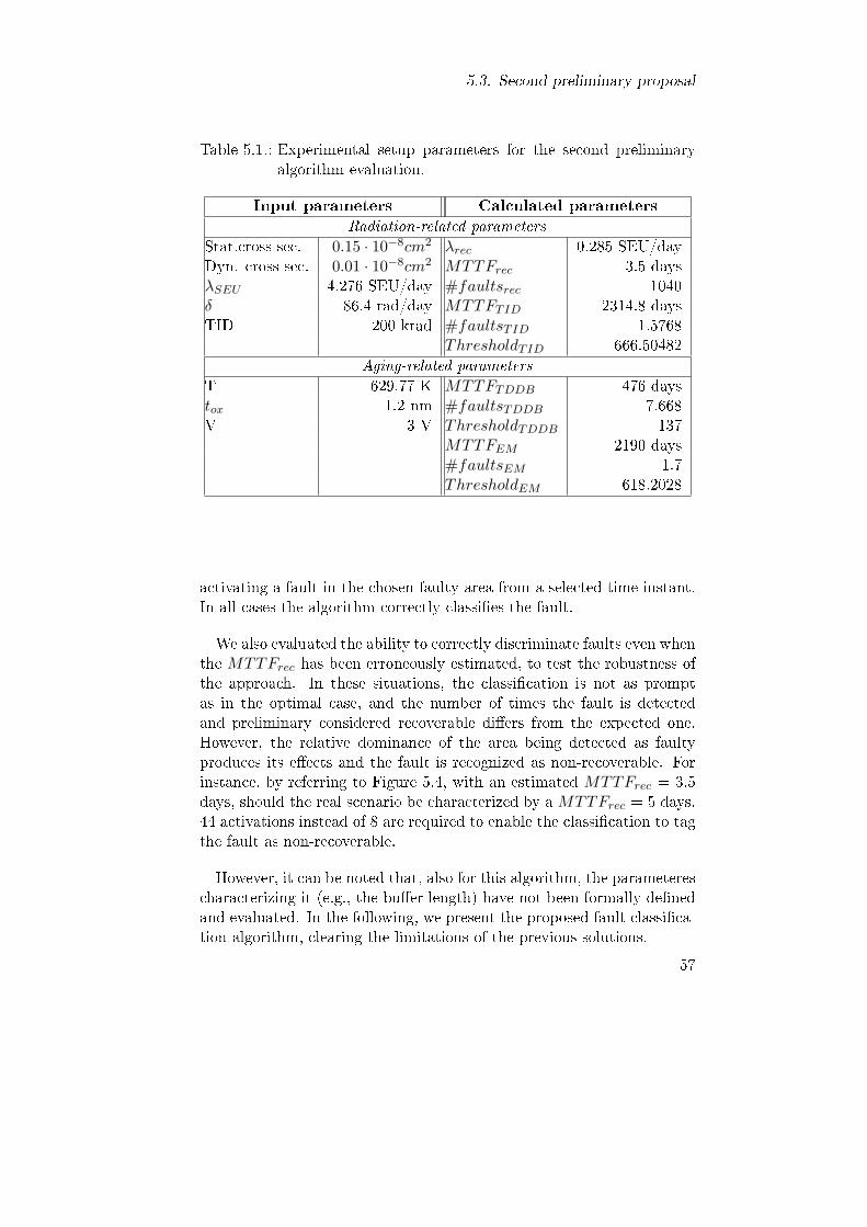
5.3. Second preliminary proposal
Table 5.1.: Experimental setup parameters for the second preliminaryalgorithm evaluation.
Input parameters Calculated parameters
Radiation-related parameters
Stat.cross sec. 0.15 · 10−8cm2 λrec 0.285 SEU/dayDyn. cross sec. 0.01 · 10−8cm2 MTTFrec 3.5 daysλSEU 4.276 SEU/day #faultsrec 1040δ 86.4 rad/day MTTFTID 2314.8 daysTID 200 krad #faultsTID 1.5768
ThresholdTID 666.50482Aging-related parameters
T 629.77 K MTTFTDDB 476 daystox 1.2 nm #faultsTDDB 7.668V 3 V ThresholdTDDB 137
MTTFEM 2190 days#faultsEM 1.7ThresholdEM 618.2028
activating a fault in the chosen faulty area from a selected time instant.In all cases the algorithm correctly classi�es the fault.
We also evaluated the ability to correctly discriminate faults even whenthe MTTFrec has been erroneously estimated, to test the robustness ofthe approach. In these situations, the classi�cation is not as promptas in the optimal case, and the number of times the fault is detectedand preliminary considered recoverable di�ers from the expected one.However, the relative dominance of the area being detected as faultyproduces its e�ects and the fault is recognized as non-recoverable. Forinstance, by referring to Figure 5.4, with an estimated MTTFrec = 3.5days, should the real scenario be characterized by a MTTFrec = 5 days,44 activations instead of 8 are required to enable the classi�cation to tagthe fault as non-recoverable.
However, it can be noted that, also for this algorithm, the parameterescharacterizing it (e.g., the bu�er length) have not been formally de�nedand evaluated. In the following, we present the proposed fault classi�ca-tion algorithm, clearing the limitations of the previous solutions.
57
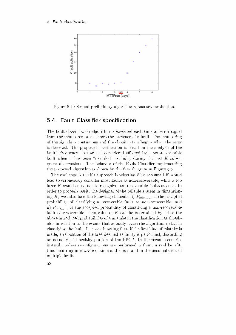
5. Fault classi�cation
Figure 5.4.: Second preliminary algorithm robustness evaluation.
5.4. Fault Classi�er speci�cation
The fault classi�cation algorithm is executed each time an error signalfrom the monitored areas shows the presence of a fault. The monitoringof the signals is continuous and the classi�cation begins when the erroris detected. The proposed classi�cation is based on the analysis of thefault's frequency. An area is considered a�ected by a non-recoverablefault when it has been �recorded� as faulty during the last K subse-quent observations. The behavior of the Fault Classi�er implementingthe proposed algorithm is shown by the �ow diagram in Figure 5.5.The challenge with this approach is selecting K; a too small K would
lead to erroneously consider most faults as non-recoverable, while a toolarge K would cause not to recognize non-recoverable faults as such. Inorder to properly assist the designer of the reliable system in dimension-ing K, we introduce the following elements: i) Pmisr−nr is the acceptedprobability of classifying a recoverable fault as non-recoverable, andii) Pmisnr−r is the accepted probability of classifying a non-recoverablefault as recoverable. The value of K can be determined by using theabove introduced probabilities of a mistake in the classi�cation as thresh-olds in relation to the events that actually cause the algorithm to fail inclassifying the fault. It is worth noting that, if the �rst kind of mistake ismade, a relocation of the area deemed as faulty is performed, discardingan actually still healthy portion of the FPGA. In the second scenario,instead, useless recon�gurations are performed without a real bene�t,thus incurring in a waste of time and e�ort, and in the accumulation ofmultiple faults.
58

5.4. Fault Classi�er speci�cation
no
yes
area = 0
area < n?
error(area)?
area++
no
yes
last_area==area? yes
fault_type = non-recoverablefault_type = recoverable
no
erro
r mon
itorin
ger
ror
dete
ctio
nfre
quen
cyve
rifica
tion
faul
t typ
eid
entifi
catio
n
Fault Classifier enabled?
yes
no
counter==K?
last_area = area
counter = 1 no yes
last_area = -1
counter = 0
counter++
Figure 5.5.: Fault Classi�er behavior
Recoverable faults are mistaken for non-recoverable ones whenever Ksubsequent recoverable faults occur all in the same area, and such eventoccurs with a probability Parea×K equal to:
Parea×K =(
1n
)K
(5.1)
Therefore, to keep the probability of a mistake within the desiredthreshold, we obtain:
K ≥ dlog 1nPmisr−nre (5.2)
In the de�nition of K, also the other kind of classi�cation mistakemust be taken into account. A fault is mistaken as recoverable if a non-recoverable one is not characterized by K subsequent detections becausea recoverable fault occurs within the sequence. As a result, as shownin Figure 5.6, to avoid this situation, the time necessary to classify anon-recoverable fault must be shorter than the time elapsing between
59

5. Fault classi�cation
Rec fault 1
Non-recfault A
lat
(K - 1) lat
MTBFrec
Rec error 1Non-recerror A
Non-recerror A
Non-recerror A
Rec error 2Rec fault 2
lat
Fault A recognizedas non-recoverable
Figure 5.6.: Non-recoverable fault classi�cation
two recoverable faults, de�ned as MTBFrec. This must be avoided as itleads to the violation of the single-error hypothesis on which this work isbased. The probability of this event occurring is related to the latencylat, that is the time for a given non-recoverable fault to produce anerror. Since for the �rst (K − 1) times the system tries to recover byrecon�guring the area assuming it to be a recoverable error, (K − 1) ·lat indicates the time necessary to recognize a non-recoverable fault,where lat is associated with that speci�c fault. Nevertheless, as statedin Chapter 3, we assume a homogeneous implementation of the systemonto the device, such that this parameter can be assumed as uniquefor all faults, using an average value. The fault, not yet classi�ed asnon-recoverable, is hereafter called not-recovered. By considering thisscenario, the probability that a recoverable fault occurs before a previous,non-recoverable one is identi�ed as such, is the following:
Plat =(K − 1) · lat
MTBFrec(5.3)
Based on this equation, the threshold K must satisfy the following con-dition:
K ≤ MTBFrec
latPmisnr−r + 1 (5.4)
By selecting a value of K which satis�es both Equation 5.2 and Equa-tion 5.4, we obtain an algorithm that correctly identi�es non-recoverablefaults with desired level of accuracy. In general, though, latency is ne-glected since the relation between fault and error is of orders of mag-nitude smaller than fault occurrence, hence Equation 5.4 could be ne-glected and no upper bound for K could be identi�ed. However, thelatency is a positive value that actually depends on the speci�c imple-mentation, so an upper bound for K must be considered. We de�ne the
60
5.5. Algorithm evaluation
optimum value of K as follows:
K = dlog 1nPmisr−nre (5.5)
The choice of considering the errors' frequency for the classi�cation issupported by the assumption that, when an area is a�ected by a non-recoverable fault, errors in that area are signaled with a higher frequencythan errors due to recoverable faults. In fact, when an error is observed,a recon�guration is triggered and, if the fault is recoverable, no erroris then detected for the subsequent time window corresponding to theMTBFrec, otherwise the recon�guration produces a bene�t only untilan input causes the fault to be observed again (an error in the same areais detected after latency lat). This situation occurs because, once weobserve an error due to a recoverable fault, we immediately recon�gurethe system, correcting the fault, and the next error will be seen when thenext recoverable fault happens (i.e., when the system is again hit by aparticle causing a SEU). Concerning errors due to non-recoverable faults,instead, they are taken care of only once recognized, which happens witha certain latency after they are �rst encountered. This means that, oncethe �rst of such errors is seen, the next one will be observed as soonas the fault propagates again to the system's outputs. More rigorously,the frequency of a recoverable fault depends on its occurrence and itsobservability, whereas a not-recovered fault (i.e., a non-recoverable faultthat has not been classi�ed as such yet) is already present in the systemand its frequency depends only on the latency related to the fault-errorrelation. As stated, this value is of orders of magnitude smaller than theMTBFrec, even for harsh environments as the space one. As a conse-quence, we derive that the MTBFrec is bigger than the time elapsingbetween observations of the same non-recoverable fault, hence we canexpect a number of not-recovered fault observations, here identi�ed asK, before a recoverable fault occurs. Since the MTTR is equal for bothrecoverable and not-recovered faults, the frequencies of recoverable andnot-recovered faults can be compared based only on their MTTFs, hencejustifying the assumption underlying to the algorithm's design.
5.5. Algorithm evaluation
This section describes the evaluation of the proposed algorithm, by pre-senting the experimental setup and results in Sections 5.5.1 and 5.5.2,respectively. Finally, the algorithm is compared with the related workand the preliminary versions in Section 5.5.3.
61
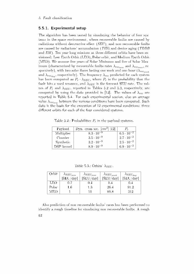
5. Fault classi�cation
5.5.1. Experimental setup
The algorithm has been tested by simulating the behavior of four sys-tems in the space environment, where recoverable faults are caused byradiations without destructive e�ect (SEU ), and non-recoverable faultsare caused by radiations' accumulation (TID) and device aging (TDDBand EM ). Ten-year long missions at three di�erent orbits have been en-visioned: Low-Earth Orbit (LEO), Polar orbit, and Medium Earth Orbit(MEO). We assume �ve years of Solar Minimum and �ve of Solar Max-imum (characterized by recoverable faults rates λrecmin and λrecmax , re-spectively), with two solar �ares lasting one week and one hour (λrecweek
and λrecday, respectively). The frequency λrec predicted for each system
has been computed as Pr · λSEU , where Pr is the probability that thefault hits a used resource, and λSEU is the forecast SEU rate. The val-ues of Pr and λSEU , reported in Tables 5.2 and 5.3, respectively, arecomputed by using the data provided in [12]. The values of λrec arereported in Table 5.4. For each experimental session, also an averagevalue λrecavg between the various conditions have been computed. Suchdata is the basis for the execution of 12 experimental conditions: threedi�erent orbits for each of the four considered systems.
Table 5.2.: Probabilities Pr in the payload systems.
Payload Dyn. cross sec. [cm2] [12] Pr
Multiplier 8.3 · 10−9 6.5 · 10−2
Counter 3.5 · 10−9 2.7 · 10−2
Synthetic 3.2 · 10−9 2.5 · 10−2
DSP kernel 8.9 · 10−9 6.9 · 10−2
Table 5.3.: Orbits' λSEU .
Orbit λSEUmin λSEUmax λSEUweekλSEUday
[SEU/day] [SEU/day] [SEU/day] [SEU/day]LEO 0.7 0.4 0.4 0.4Polar 1.6 1.3 26.4 91.2MEO 1 11 88.8 312
Also prediction of non-recoverable faults' rates has been performed toidentify a rough timeline for simulating non-recoverable faults. A rough
62

5.5. Algorithm evaluation
Table 5.4.: Predicted λrec at the considered environmental conditions.
Orbit λrecmin λrecmax λrecweekλrecday
[SEU/day] [SEU/day] [SEU/day] [SEU/day]Multiplier
exp1 LEO 4.5 · 10−2 2.6 · 10−2 2.6 · 10−2 2.6 · 10−2
exp2 Polar 10.4 · 10−2 8.4 · 10−2 171.6 · 10−2 592.8 · 10−2
exp3 MEO 6.5 · 10−2 71.5 · 10−2 577.2 · 10−2 2028.0 · 10−2
Counterexp4 LEO 1.9 · 10−2 1.1 · 10−2 1.1 · 10−2 1.1 · 10−2
exp5 Polar 4.3 · 10−2 3.5 · 10−2 71.3 · 10−2 246.2 · 10−2
exp6 MEO 2.7 · 10−2 29.7 · 10−2 239.8 · 10−2 842.4 · 10−2
Syntheticexp7 LEO 1.7 · 10−2 10−2 10−2 10−2
exp8 Polar 4.0 · 10−2 3.2 · 10−2 66.0 · 10−2 228.0 · 10−2
exp9 MEO 2.5 · 10−2 27.5 · 10−2 222.0 · 10−2 780.0 · 10−2
DSP kernelexp10 LEO 4.8 · 10−2 2.8 · 10−2 2.8 · 10−2 2.8 · 10−2
exp11 Polar 11.0 · 10−2 9.0 · 10−2 182.2 · 10−2 629.3 · 10−2
exp12 MEO 6.9 · 10−2 75.9 · 10−2 612.7 · 10−2 2152.8 · 10−2
0 5 8 10
Timeline [years]
Solar Minimum Solar Maximum
Worst dayWorst week
Non-recoverable faults[days]
TDDB
TID
EM
410 820 1230 1640 2050 2460 2870 3280 34701388 35600
Figure 5.7.: Non-recoverable faults' timeline.
prediction is su�cient since the algorithm accuracy in identifying non-recoverable faults does not depend on their time occurrence. The rateof non-recoverable faults due to TID e�ect is computed by consideringa predicted dose rate of 86.4 rad/day [55] and, by taking into account aXilinx FPGA XCV1000, a TID of 60 krad [56]; we obtain MTBFTID
= 694 days. Finally, we have considered the MTBFs due to device agingcomputed in [19], i.e., MTBFTDDB = 410 days and MTBFEM = 1460days. The timeline of the predicted non-recoverable faults is shown inFigure 5.7.
63
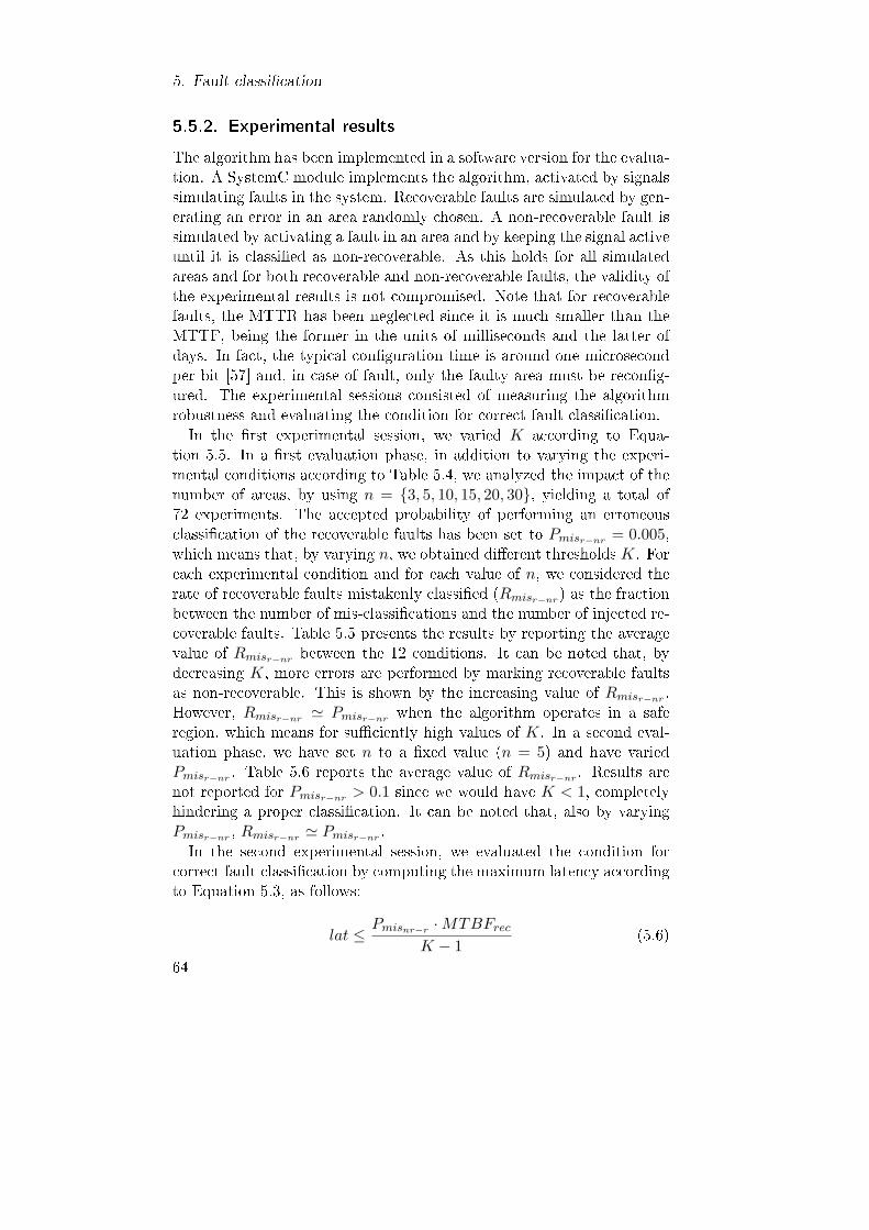
5. Fault classi�cation
5.5.2. Experimental results
The algorithm has been implemented in a software version for the evalua-tion. A SystemC module implements the algorithm, activated by signalssimulating faults in the system. Recoverable faults are simulated by gen-erating an error in an area randomly chosen. A non-recoverable fault issimulated by activating a fault in an area and by keeping the signal activeuntil it is classi�ed as non-recoverable. As this holds for all simulatedareas and for both recoverable and non-recoverable faults, the validity ofthe experimental results is not compromised. Note that for recoverablefaults, the MTTR has been neglected since it is much smaller than theMTTF, being the former in the units of milliseconds and the latter ofdays. In fact, the typical con�guration time is around one microsecondper bit [57] and, in case of fault, only the faulty area must be recon�g-ured. The experimental sessions consisted of measuring the algorithmrobustness and evaluating the condition for correct fault classi�cation.In the �rst experimental session, we varied K according to Equa-
tion 5.5. In a �rst evaluation phase, in addition to varying the experi-mental conditions according to Table 5.4, we analyzed the impact of thenumber of areas, by using n = {3, 5, 10, 15, 20, 30}, yielding a total of72 experiments. The accepted probability of performing an erroneousclassi�cation of the recoverable faults has been set to Pmisr−nr = 0.005,which means that, by varying n, we obtained di�erent thresholds K. Foreach experimental condition and for each value of n, we considered therate of recoverable faults mistakenly classi�ed (Rmisr−nr) as the fractionbetween the number of mis-classi�cations and the number of injected re-coverable faults. Table 5.5 presents the results by reporting the averagevalue of Rmisr−nr between the 12 conditions. It can be noted that, bydecreasing K, more errors are performed by marking recoverable faultsas non-recoverable. This is shown by the increasing value of Rmisr−nr .However, Rmisr−nr ' Pmisr−nr when the algorithm operates in a saferegion, which means for su�ciently high values of K. In a second eval-uation phase, we have set n to a �xed value (n = 5) and have variedPmisr−nr . Table 5.6 reports the average value of Rmisr−nr . Results arenot reported for Pmisr−nr > 0.1 since we would have K < 1, completelyhindering a proper classi�cation. It can be noted that, also by varyingPmisr−nr , Rmisr−nr ' Pmisr−nr .In the second experimental session, we evaluated the condition for
correct fault classi�cation by computing the maximum latency accordingto Equation 5.3, as follows:
lat ≤Pmisnr−r ·MTBFrec
K − 1(5.6)
64
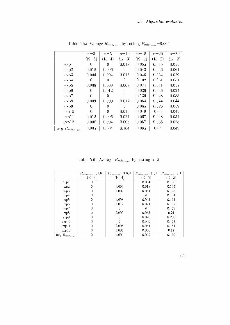
5.5. Algorithm evaluation
Table 5.5.: Average Rmisr−nr by setting Pmisr−nr=0.005
n=3 n=5 n=10 n=15 n=20 n=30(K=5) (K=4) (K=3) (K=2) (K=2) (K=2)
exp1 0 0 0.018 0.055 0.046 0.055exp2 0.018 0.006 0 0.043 0.036 0.061exp3 0.004 0.004 0.013 0.046 0.034 0.029exp4 0 0 0 0.102 0.051 0.051exp5 0.008 0.008 0.008 0.074 0.041 0.057exp6 0 0.012 0 0.036 0.036 0.024exp7 0 0 0 0.139 0.028 0.083exp8 0.009 0.009 0.017 0.053 0.044 0.044exp9 0 0 0 0.065 0.026 0.052exp10 0 0 0.016 0.049 0.05 0.049exp11 0.012 0.006 0.024 0.067 0.048 0.054exp12 0.008 0.004 0.008 0.057 0.036 0.028
avg Rmisr−nr 0.005 0.004 0.104 0.065 0.04 0.049
Table 5.6.: Average Rmisr−nr by setting n=5
Pmisr−nr=0.001 Pmisr−nr=0.004 Pmisr−nr=0.01 Pmisr−nr=0.1(K=5) (K=4) (K=3) (K=2)
exp1 0 0 0.064 0.156exp2 0 0.006 0.018 0.165exp3 0 0.004 0.034 0.143exp4 0 0 0 0.154exp5 0 0.008 0.033 0.164exp6 0 0.012 0.024 0.167exp7 0 0 0 0.167exp8 0 0.009 0.053 0.21exp9 0 0 0.026 0.208exp10 0 0 0.049 0.164exp11 0 0.006 0.054 0.164exp12 0 0.004 0.036 0.17
avg Rmisr−nr 0 0.003 0.032 0.169
65

5. Fault classi�cation
This condition should guide the designer when de�ning the system, char-acterized by a fault-error relation respecting the maximum latency. Forthe values of K estimated in the previous experimental session, we com-puted the latency by setting su�ciently low values of the misclassi�ca-tion error probability, Pmisnr−r = {0.005, 0.01, 0.05, 0.1}, and computingMTBFrec = 1
λrec, where λrec is the worst value between the environmen-
tal conditions. Table 5.7 presents the results by reporting the averagevalue of lat in the 12 conditions. Results show fault classi�cation suc-ceeds even with lat up to the order of hours (with a few exceptions inthe range of tens of minutes), which is a very high value consideringa typical fault-error relation, thus con�rming the algorithm rationale.Moreover, it should be taken into account that we considered very strictvalues for MTBFrec, by considering the worst case between the variousenvironmental conditions. Hence, the latency required for correct faultclassi�cation is even higher than the one computed. Finally, it shouldbe noticed that the latency increases when raising the value of Pmisnr−r ,that can be higher than the selected Pmisr−nr since mistaking a faultas recoverable is less serious than mistaking it as non-recoverable. Infact, in the latter case, we discard an actually still healthy portion ofthe FPGA. In all cases, the latency is in the order of hours also at highorbits, where faults are more frequent. In most cases, several hours areallowed for fault detection and recovery.
5.5.3. Comparison with related work
The proposed algorithm has been compared with the related work andthe preliminary versions. No comparison with the �rst preliminary ver-sion of the algorithm has been performed since no indication for settingthe parameters characterizing the algorithm has been provided.The approach in [52] can be considered equivalent to ours when K
is set to 2, if we do not �x a MTBF (not so easily predictable). Suchvalue of K is suitable when the number of areas is high enough (greaterthan 10, according to our approach), otherwise it is possible to fall intoa mis-classi�cation of a recoverable fault as non-recoverable.The algorithm in [53], targeted for microprocessors, is quite similar to
ours. Both approaches count the number of faults a�ecting the areas andidentify hard faults when a prede�ned threshold is exceeded. We veri�edthat by setting the period for clearing the counters as MTBF of recov-erable faults and the threshold as K, the algorithm in [53] has the sameclassi�cation performance as ours. However, our approach only requiresthe use of one counter of length K, whereas, in [53], it is necessary to setas many counters as the areas, whose number can be very high; counters
66
5.5. Algorithm evaluation
Table 5.7.: Average latency [hour]
K = 2 K = 3 K = 4 K = 5exp1 73.85 36.92 24.61 18.46exp2 24.61 12.31 8.21 6.15exp3 6.05 3.03 2.02 1.51exp4 177.78 88.89 59.26 44.44exp5 59.26 29.63 19.75 14.81exp6 14.57 7.29 4.86 3.64exp7 192.00 96.00 64.00 48.00exp8 64.00 32.00 21.33 16.00exp9 15.74 7.87 5.25 3.93exp10 69.57 34.78 23.19 17.39exp11 23.19 11.59 7.73 5.80exp12 5.70 2.85 1.90 1.43
Pmisnr−r=0.005 1.54 0.77 0.51 0.39Pmisnr−r=0.01 3.09 1.54 1.03 0.77Pmisnr−r=0.05 15.45 7.72 5.15 3.86Pmisnr−r=0.1 30.90 15.45 10.30 7.72
can considerably impact the area occupation of the Fault Classi�er bothfor their number and for the hardening process. Moreover, the structureof our algorithm enables a formal and rigorous study of the e�ect of eachparameter.
Finally, we have taken into account the second preliminary version ofthe algorithm. We have considered that a fault occurs relatively morefrequently than the others when only the faulty area is registered in abu�er of length K. Moreover, we have computed the thresholds relatedto non-recoverable faults to analyze their absolute frequency, by consid-ering the values reported in the previous section. We have evaluatedsuch algorithm by considering the number of fault observations requiredto classify the fault as non-recoverable and by comparing it with K,as shown in Figure 5.8. Results show that, in the second preliminaryversion, the number of fault observations to recognize a non-recoverablefault can be very high, whereas in the proposed solution is �xed.
67

5. Fault classi�cation
0
25
50
75
100
Num
ber
ofobse
rvati
ons
exp1
exp2
exp3
exp4
exp5
exp6
exp7
exp8
exp9
exp1
0
exp1
1
exp1
2
Experiment
Proposed
Version 2
Figure 5.8.: Comparison of the number of fault observations to recognizea non-recoverable fault in the proposed solution and the sec-ond preliminary version of the algorithm.
5.6. Chapter summary
In this chapter, an algorithm for the distinction between recoverable andnon-recoverable faults has been designed. With respect to the otherworks proposed in literature, we formally de�ne the parameters char-acterizing the fault classi�cation algorithm and present rigorous mecha-nisms for dimensioning them based on the desired classi�cation accuracy.Two preliminary versions of the algorithm have been proposed and a �nalsolution has been accurately evaluated. Experimental results show thatthe proposed algorithm recognizes non-recoverable faults with desiredlevel of accuracy and prove the e�ectiveness of the algorithm also withrespect to related work. The algorithm has been designed and tested forspace applications, being space the target scenario of the thesis, but thework is suitable for any application that must tolerate both recoverableand non-recoverable faults. The proposed algorithm is implemented bythe Fault Classi�er module of the Recon�guration Controller, presentedin the next chapter.
68
6. Recon�guration Controller
design
This chapter proposes the design of the controller in charge of manag-ing the fault recovery of the multi-FPGA platform, contributing to thecreation of the reliable system. We here introduce a reliability-awareRecon�guration Controller, aimed at performing the fault classi�cationpresented in the previous chapter and managing the recon�guration pro-cess of the faulty parts of the architecture to mitigate fault e�ects.The Recon�guration Controller is the main component responsible for
the active fault mitigation process. It continuously monitors the errorsignals from the neighbor FPGA and, upon error detection, triggers arecon�guration, based on the classi�cation of the fault nature (recover-able vs. non-recoverable). Should the fault be considered as recoverable,the FPGA is partially recon�gured by reloading the bitstream portionrelated to the faulty area, otherwise the faulty area is relocated to a spareregion by loading a new bitstream. Such recovery action by means ofrecon�guration requires few seconds, and even few milliseconds in caseof recoverable fault, being the typical con�guration time around one mi-crosecond per bit [57]. It is worth noting that the proposed approach issuitable for stateless applications, since the application must be stoppedin case of non-recoverable fault; alternative solutions can be investigatedas future work.Indeed, it is necessary to prevent erroneous recon�gurations by de-
tecting also faults a�ecting the Recon�guration Controller itself. Hence,fault detection capability is required for the Recon�guration Controller,also. More precisely, the controller itself can be seen as an area that,in case of fault, is recovered or relocated based on the type of occurredfault.The chapter is organized as follows: Section 6.1 describes the related
work on controller design. Section 6.2 introduces a software implementa-tion developed to validate the designed controller with respect to its re-quirements, and Section 6.3 proposes a preliminary hardware reliability-aware implementation. Section 6.4 presents the design of the proposedsolution and Section 6.5 describes the hardening of the module. Finally,Section 6.6 draws �nal considerations.
69
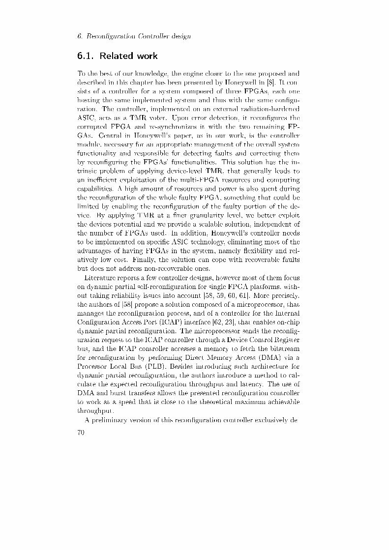
6. Recon�guration Controller design
6.1. Related work
To the best of our knowledge, the engine closer to the one proposed anddescribed in this chapter has been presented by Honeywell in [8]. It con-sists of a controller for a system composed of three FPGAs, each onehosting the same implemented system and thus with the same con�gu-ration. The controller, implemented on an external radiation-hardenedASIC, acts as a TMR voter. Upon error detection, it recon�gures thecorrupted FPGA and re-synchronizes it with the two remaining FP-GAs. Central in Honeywell's paper, as in our work, is the controllermodule, necessary for an appropriate management of the overall systemfunctionality and responsible for detecting faults and correcting themby recon�guring the FPGAs' functionalities. This solution has the in-trinsic problem of applying device-level TMR, that generally leads toan ine�cient exploitation of the multi-FPGA resources and computingcapabilities. A high amount of resources and power is also spent duringthe recon�guration of the whole faulty FPGA, something that could belimited by enabling the recon�guration of the faulty portion of the de-vice. By applying TMR at a �ner granularity level, we better exploitthe devices potential and we provide a scalable solution, independent ofthe number of FPGAs used. In addition, Honeywell's controller needsto be implemented on speci�c ASIC technology, eliminating most of theadvantages of having FPGAs in the system, namely �exibility and rel-atively low cost. Finally, the solution can cope with recoverable faultsbut does not address non-recoverable ones.Literature reports a few controller designs, however most of them focus
on dynamic partial self-recon�guration for single FPGA platforms, with-out taking reliability issues into account [58, 59, 60, 61]. More precisely,the authors of [58] propose a solution composed of a microprocessor, thatmanages the recon�guration process, and of a controller for the InternalCon�guration Access Port (ICAP) interface [62, 23], that enables on-chipdynamic partial recon�guration. The microprocessor sends the recon�g-uration request to the ICAP controller through a Device Control Registerbus, and the ICAP controller accesses a memory to fetch the bitstreamfor recon�guration by performing Direct Memory Access (DMA) via aProcessor Local Bus (PLB). Besides introducing such architecture fordynamic partial recon�guration, the authors introduce a method to cal-culate the expected recon�guration throughput and latency. The use ofDMA and burst transfers allows the presented recon�guration controllerto work at a speed that is close to the theoretical maximum achievablethroughput.A preliminary version of this recon�guration controller exclusively de-
70
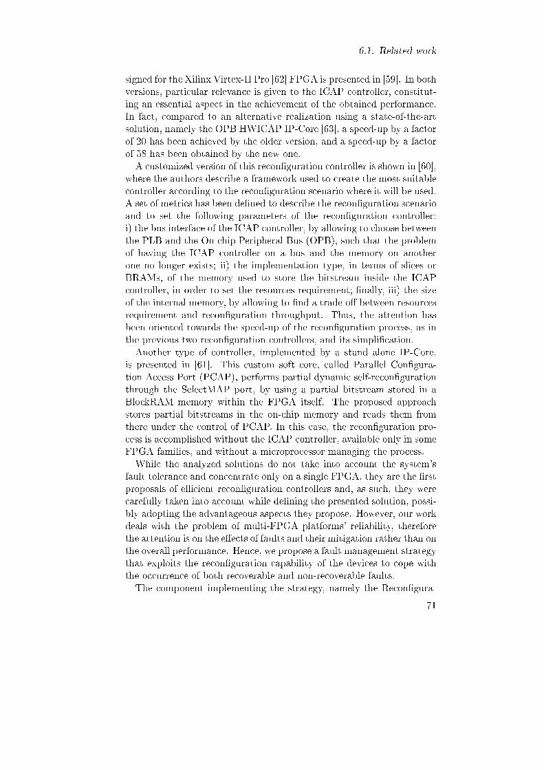
6.1. Related work
signed for the Xilinx Virtex-II Pro [62] FPGA is presented in [59]. In bothversions, particular relevance is given to the ICAP controller, constitut-ing an essential aspect in the achievement of the obtained performance.In fact, compared to an alternative realization using a state-of-the-artsolution, namely the OPB HWICAP IP-Core [63], a speed-up by a factorof 20 has been achieved by the older version, and a speed-up by a factorof 58 has been obtained by the new one.A customized version of this recon�guration controller is shown in [60],
where the authors describe a framework used to create the most suitablecontroller according to the recon�guration scenario where it will be used.A set of metrics has been de�ned to describe the recon�guration scenarioand to set the following parameters of the recon�guration controller:i) the bus interface of the ICAP controller, by allowing to choose betweenthe PLB and the On-chip Peripheral Bus (OPB), such that the problemof having the ICAP controller on a bus and the memory on anotherone no longer exists; ii) the implementation type, in terms of slices orBRAMs, of the memory used to store the bitstream inside the ICAPcontroller, in order to set the resources requirement; �nally, iii) the sizeof the internal memory, by allowing to �nd a trade-o� between resourcesrequirement and recon�guration throughput. Thus, the attention hasbeen oriented towards the speed-up of the recon�guration process, as inthe previous two recon�guration controllers, and its simpli�cation.Another type of controller, implemented by a stand alone IP-Core,
is presented in [61]. This custom soft core, called Parallel Con�gura-tion Access Port (PCAP), performs partial dynamic self-recon�gurationthrough the SelectMAP port, by using a partial bitstream stored in aBlockRAM memory within the FPGA itself. The proposed approachstores partial bitstreams in the on-chip memory and reads them fromthere under the control of PCAP. In this case, the recon�guration pro-cess is accomplished without the ICAP controller, available only in someFPGA families, and without a microprocessor managing the process.While the analyzed solutions do not take into account the system's
fault tolerance and concentrate only on a single FPGA, they are the �rstproposals of e�cient recon�guration controllers and, as such, they werecarefully taken into account while de�ning the presented solution, possi-bly adopting the advantageous aspects they propose. However, our workdeals with the problem of multi-FPGA platforms' reliability, thereforethe attention is on the e�ects of faults and their mitigation rather than onthe overall performance. Hence, we propose a fault management strategythat exploits the recon�guration capability of the devices to cope withthe occurrence of both recoverable and non-recoverable faults.The component implementing the strategy, namely the Recon�gura-
71
6. Recon�guration Controller design
tion Controller, has been designed, by identifying its functionality andfeatures. Innovative points of the presented solution are:
• distributed, low cost Recon�guration Controller, eliminating theneed to deploy it on ad-hoc device,
• management of both recoverable and non-recoverable faults, and
• scalable use of multiple FPGAs to build a recon�gurable reliablesystem.
A preliminary software implementation has been developed to validatethe designed controller with respect to its requirements, and two hard-ware reliability-aware solutions have been proposed, as described in thenext sections.
6.2. Software implementation
Both software and hardware implementations of the Recon�gurationController have been taken into account, to identify the most convenientsolution, based also on the available FPGA platform. A preliminarysoftware implementation has been developed and deployed for a boardhosting a microprocessor, to re�ne the controller behavior and to verifythe external recon�guration aspect, triggered by the error detection.The software-based system implementing the Recon�guration Con-
troller is shown in Figure 6.1. The Recon�guration Controller is imple-mented by a MicroBlaze, that monitors the error signals from the otherFPGA(s) through a General Purpose I/O (GPIO) component. In caseof fault of a monitored FPGA, it takes the correct bitstream stored in anSRAM memory and performs the recon�guration of the faulty portionof the system through a JTAG component, that communicates with theother FPGA through the con�guration link. The bitstreams are storedin the SRAM memory through UART RS232 and the communication be-tween all components is performed through OPB bus. The code executedby the MicroBlaze is stored in a BRAM memory that communicates withthe processor through Local Memory Bus.The design and prototype implementation of the Recon�guration Con-
troller have been de�ned using as a preliminary platform two Spartan-3AFPGAs. One FPGA hosts the Recon�guration Controller and the otherone the system with fault detection properties. When a fault occurs inthe monitored system, the Recon�guration Controller performs the re-con�guration of the system. The two FPGAs are connected through twophysical links, one for con�guration and one for communication. The
72
6.2. Software implementation
MicroBlazeBRAM
SRAM
JTAGUART RS232
Arbiter Bus
Local Memory Bus
GPIO
Figure 6.1.: First prototype of Recon�guration Controller.
con�guration link is obtained through the use of a cable attached to theA2 Expansion Connector of the Recon�guration Controller board andthe JTAG of the monitored system board, while the communication linkuses a cable attached to the A2 Expansion Connectors of the two boards,as shown in Figure 6.2.
FPGA
A2 Expansion C
onnector
JTAGReconfiguration Controller board
FPGA
A2 E
xpan
sion
C
onne
ctor
JTAG
Monitored system board
Configuration link
Communication link
Figure 6.2.: Software-based implemented prototype platform.
The system monitored by the Recon�guration Controller consists ofa counter on which the TMR is applied, as shown in Figure 6.3. Thecounter computation is shown on the 7 segment display hosted on theboard, and the outputs of the 3 counters are sent to a voter. The voterhas been modi�ed to support the fault generation, simulated by pressinga button on the board. The error signals are sent to the Recon�gurationController FPGA through the communication link.When the Recon�guration Controller detects an error, it performs the
73

6. Recon�guration Controller design
COUNTER A
clk
reset
output
COUNTER B
clk
reset
COUNTER C
clk
reset
VOTER
input1
error_gen
output
errinput2input3
clk
reset
error_gen
output
output
x
x
Figure 6.3.: Reliable system.
recon�guration of the other FPGA by using the appropriate bitstream.The recon�guration with di�erent bitstreams has been tested by creatingtwo versions of the counter; in the �rst version (bitstream 1) the countis from 0 to 9, while in the second one (bitstream 2) the count considersonly even numbers. Bitstream 1 is loaded when fault occurs while 0, 1, 4or 6 are displayed on the second board, otherwise bitstream 2 is loaded.
Two are the main limitations characterizing a software implementa-tion, namely the sharing of the microprocessor with the application be-ing normally executed, and the hardening against faults. As far as theformer aspect is concerned, should the available microprocessor be ex-ploited to run the nominal application (otherwise the platform would nothost a microprocessor, to begin with), the fault mitigation managementapplication would have to be executed periodically, during idle time, thusintroducing a latency in fault detection and management. Consideringthe latter aspect, the prototype did not expose reliability features, sincehardening by means of software-based techniques is expensive in termsof overhead (code and performance degradation) as well as it only al-lows for a partially reliable system [64]. A possible solution to achievethe necessary reliability consists in adopting a fault tolerant IP, such asLeon2-FT [65]. However, the �nal cost is quite prohibitive, with an oc-cupation of available resources on an xc2v3000 FPGA requiring about24% registers, 37% Block RAMs and 79% LUTs. For these reasons, ahardware solution, whose design is presented in the next sections, hasbeen preferred.
74

6.3. Preliminary proposal
6.3. Preliminary proposal
In our preliminary proposal, presented in [50], the fault detection ca-pability required for the Recon�guration Controller is guaranteed bymeans of readback; each Recon�guration Controller of the system pe-riodically accesses the neighbor FPGA to perform the partial readbackof the con�guration memory corresponding to the controller, to detect,and eventually repair, faults. Thus, the main tasks of the controller are:i) continuously monitoring the neighbor FPGA's error signals from theapplication areas, ii) periodically monitoring the controller hosted onthe neighbor FPGA, and iii) upon error detection in one of the areas,application ones or controller, trigger a recon�guration, based on theclassi�cation of the fault nature. The �ow diagram shown in Figure 6.4reports the behavior of the Recon�guration Controller.
app. areas corrupted?
time to check RC?
no
performreadback RC
RC corrupted?
yes
no
no yes classifyfault
is recoverable?
partial reconfigurationdata retrieval
complete reconfigurationdata retrieval
reconfigure
yes no
erro
r mon
itorin
gfa
ult m
itiga
tion
yes
Figure 6.4.: Recon�guration Controller �ow diagram.
In order to carry out such tasks, the following modules have beenidenti�ed as fundamental �building blocks�: Recon�guration Interface, incharge of performing the physical implementation of the recon�gurationprocess, providing access to the FPGA con�guration memory interface,andManager, to control the Recon�guration Interface based on error de-tection and classi�cation policies, determining what bitstream shall beused to recon�gure the platform and mitigate (recover or relocate) thee�ect of the fault. The Manager is, in turn, composed of the followingelements: i) a Readback Module, for the neighbor controller veri�cation,
75
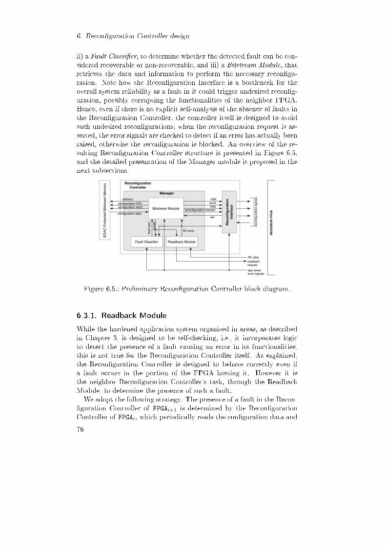
6. Recon�guration Controller design
ii) a Fault Classi�er, to determine whether the detected fault can be con-sidered recoverable or non-recoverable, and iii) a Bitstream Module, thatretrieves the data and information to perform the necessary recon�gu-ration. Note how the Recon�guration Interface is a bottleneck for theoverall system reliability as a fault in it could trigger undesired recon�g-uration, possibly corrupting the functionalities of the neighbor FPGA.Hence, even if there is no explicit self-analysis of the absence of faults inthe Recon�guration Controller, the controller itself is designed to avoidsuch undesired recon�gurations; when the recon�guration request is as-serted, the error signals are checked to detect if an error has actually beenraised, otherwise the recon�guration is blocked. An overview of the re-sulting Recon�guration Controller structure is presented in Figure 6.5,and the detailed presentation of the Manager module is proposed in thenext subsections.
Fault Classifier Readback Module
Bitstream Module
readbackrequest
RC data
RC error
faul
t typ
e Rec
onfig
urat
ion
Inte
rfac
e
FARworddata
reconfiguration request
app areas error signals
EDAC
Pro
tect
ed B
itstre
am M
emor
y
addressconfiguration FAR
configuration data
Manager
ReconfigurationController
ack
enab
le
NEI
GH
BO
R F
PGA
configuration word
reco
nfigu
ratio
n si
gnal
s
Figure 6.5.: Preliminary Recon�guration Controller block diagram.
6.3.1. Readback Module
While the hardened application system organized in areas, as describedin Chapter 3, is designed to be self-checking, i.e., it incorporates logicto detect the presence of a fault causing an error in its functionalities,this is not true for the Recon�guration Controller itself. As explained,the Recon�guration Controller is designed to behave correctly even ifa fault occurs in the portion of the FPGA hosting it. However it isthe neighbor Recon�guration Controller's task, through the ReadbackModule, to determine the presence of such a fault.We adopt the following strategy. The presence of a fault in the Recon-
�guration Controller of FPGAi+1 is determined by the Recon�gurationController of FPGAi, which periodically reads the con�guration data and
76
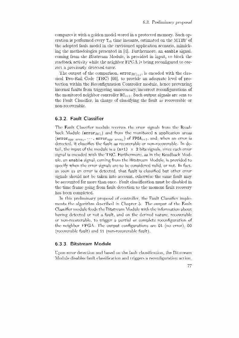
6.3. Preliminary proposal
compares it with a golden model stored in a protected memory. Such op-eration is performed every Trb time instants, estimated on the MTBF ofthe adopted fault model in the envisioned application scenario, mimick-ing the methodologies presented in [4]. Furthermore, an enable signal,coming from the Bitstream Module, is provided in input, to block thereadback activity while the neighbor FPGA is being recon�gured to cor-rect a previously detected error.The output of the comparison, errorRCi+1 , is encoded with the clas-
sical Two-Rail Code (TRC) [66], to provide an adequate level of pro-tection within the Recon�guration Controller module, hence preventinginternal faults from triggering unnecessary/incorrect recon�gurations ofthe monitored neighbor controller RCi+1. Such output signals are sent tothe Fault Classi�er, in charge of classifying the fault as recoverable ornon-recoverable.
6.3.2. Fault Classi�er
The Fault Classi�er module receives the error signals from the Read-back Module (errorRCi) and from the monitored n application areas(errorapp area1 , · · · , errorapp arean) of FPGAi+1, and, when an error isdetected, it classi�es the fault as recoverable or non-recoverable. In de-tail, the input of the module is a (n+1) × 2 bits signals, since each errorsignal is encoded with the TRC. Furthermore, as in the Readback Mod-ule, an enable signal, coming from the Bitstream Module, is provided tospecify when the error signals are to be considered valid, or not. In fact,as soon as an error is detected, that fault is classi�ed but other errorsignals should not be taken into account, otherwise the same fault maybe accounted for more than once. Fault classi�cation must be disabled inthe time frame going from fault detection to the moment fault recoveryhas been completed.In this preliminary proposal of controller, the Fault Classi�er imple-
ments the algorithm described in Chapter 5. The output of the FaultClassi�er module feeds the Bitstream Module with the information abouthaving detected or not a fault, and on the derived nature, recoverableor non-recoverable, to trigger a partial or complete recon�guration ofthe neighbor FPGA. The output con�gurations are 01 (no error), 00(recoverable fault) and 11 (non-recoverable fault).
6.3.3. Bitstream Module
Upon error detection and based on the fault classi�cation, the BitstreamModule disables fault classi�cation and triggers a recon�guration action,
77
6. Recon�guration Controller design
accessing the protected memory to retrieve the appropriate con�gurationdata. With such information, it programs the Recon�guration Interfaceto carry out the FPGA (partial) recon�guration to recover from thefault. The bitstreams are organized in memory as follows: the �rstbitstream consists of the current con�guration of the monitored FPGAand is used for partial recon�guration in case of a recoverable fault. Theother bitstreams are used to recover from non-recoverable faults, eachone of them appropriate for the detected faulty area.To implement such functionality, inputs to the Bitstream Module
are the fault type, application areas error, and RC error signals.When necessary, the Bitstream Module interacts with the memory toretrieve the desired (partial) bitstream, configuration data, to be for-warded to the Recon�guration Interface, together with a reconfigurationrequest, in terms of FAR, word, and data (i.e., the information neces-sary to perform the recon�guration). An acknowledge signal, ack, isused to increase the Recon�guration Controller reliability, by having anadditional �ag to check that recon�guration has been performed cor-rectly. When the ack is received it means that fault recovery is completeand fault classi�cation can be re-enabled (through enable signal), thusrestoring the system to its nominal behavior.
6.3.4. Solution evaluation: limits
The designed Recon�guration Controller is the �rst proposal of con-troller managing both recoverable and non-recoverable faults. It is adistributed, low cost engine, eliminating the need to deploy it on ad-hocdevice and allowing scalable use of multiple FPGAs to build a recon�g-urable reliable system.In this �rst proposal, the reliability of the controller is guaranteed
by means of readback, that is an expensive operation and subject toerrors. Thus, we investigated the reliable implementation of the engine,as described in the next section.
6.4. Proposed solution
The design and prototype implementation of the proposed Recon�gura-tion Controller have been de�ned using as a preliminary platform theone presented in Section 6.2, where each FPGA is connected to theother through the physical links for con�guration and communication.The recovery bitstreams are stored for each device in an XCF02S se-rial con�guration Flash PROM, that, besides con�guration data, canpossibly store additional non-volatile data. Each FPGA hosts both the
78
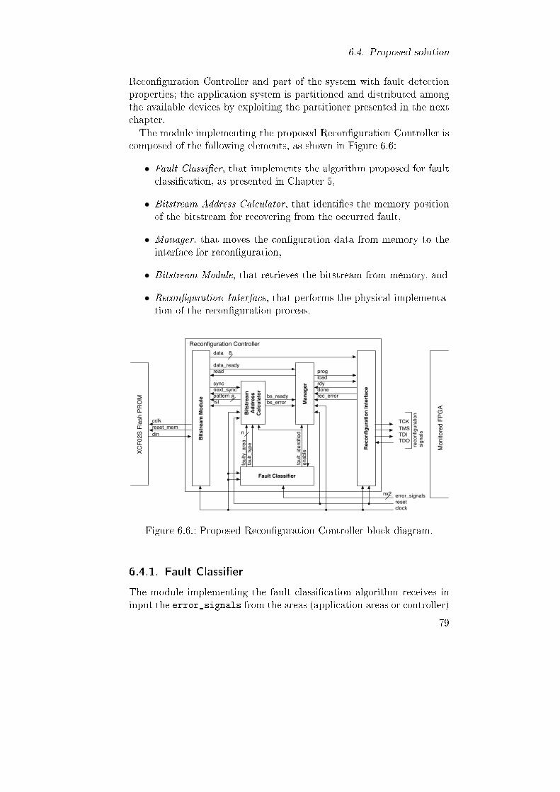
6.4. Proposed solution
Recon�guration Controller and part of the system with fault detectionproperties; the application system is partitioned and distributed amongthe available devices by exploiting the partitioner presented in the nextchapter.The module implementing the proposed Recon�guration Controller is
composed of the following elements, as shown in Figure 6.6:
• Fault Classi�er, that implements the algorithm proposed for faultclassi�cation, as presented in Chapter 5,
• Bitstream Address Calculator, that identi�es the memory positionof the bitstream for recovering from the occurred fault,
• Manager, that moves the con�guration data from memory to theinterface for recon�guration,
• Bitstream Module, that retrieves the bitstream from memory, and
• Recon�guration Interface, that performs the physical implementa-tion of the recon�guration process.
Fault Classifier
Bits
trea
m M
odul
e
Rec
onfig
urat
ion
Inte
rfac
e
faul
t_id
entifi
ed
faul
t_ty
pefa
ulty
_are
a
enab
le
data
data_ready
sync
read
pattern
progloadrdydonerec_error
TCKTMSTDITDO
error_signalsresetclock
reco
nfigu
ratio
nsi
gnal
scclkreset_memdin
XCF0
2S F
lash
PR
OM
Mon
itore
d FP
GA
Reconfiguration Controller
nx2
8
Man
ager
Bits
trea
mA
ddre
ssC
alcu
lato
r
n
bs_readybs_error
8rst
next_sync
Figure 6.6.: Proposed Recon�guration Controller block diagram.
6.4.1. Fault Classi�er
The module implementing the fault classi�cation algorithm receives ininput the error_signals from the areas (application areas or controller)
79

6. Recon�guration Controller design
and an enable signal specifying when the error signals are to be con-sidered valid (the Fault Classi�er is disabled during the recovery phase).We assume that on the error signals the areas adopt TRC, whereas theenable signal, generated within the Recon�guration Controller, is notencoded since the presence of faults in the overall controller is revealedby an error signal generated by the controller itself. The Fault Clas-si�er generates three outputs: fault_identified to signal whether afault has been detected, fault_type to specify whether it is recover-able or not, and faulty_area to specify the area where the fault hasoccurred. The entire information is then used to trigger the appropriaterecon�guration/relocation strategy, managed by the module in chargeof executing the re-programming of the neighbor FPGA. The input sig-nals are used, together with the following local information, to classifythe fault upon detection of an error condition on the input signals fromthe monitored areas: last_ira to specify the area identi�ed as faultythe last time an error has been detected, error_counter to identifythe number of consecutive errors detected on the area speci�ed in theabove mentioned register, and the parameter K to specify the thresh-old for classifying a fault as non recoverable. The resulting structureof the nominal Fault Classi�er module is reported in Figure 6.7. It ispossible to identify the internal signals used to characterize the situa-tion, error_detected (when an area is identi�ed as faulty), same_area(whether the area identi�ed as faulty is the same as the last detectedarea), and max_count (whether the number of consecutive fault detec-tions in the same area has reached the pre-de�ned threshold K). Thesesignals are used to de�ne the control of the entire module, describedin terms of the FSM reported in Figure 6.8. The FSM generates theinternal clock and reset signals (namely clk and rst) used to controlthe module evolution, and the (re)setting of the instantiated registers.A VHDL description of the module has been developed for simulationand synthesis purposes. Figure 6.9 reports the waveforms of the modulebehavior following the detection of a non-recoverable fault.
6.4.2. Bitstream Address Calculator
The Bitstream Address Calculator is in charge of identifying the mem-ory position of the con�guration data for fault recovery. When thefault_identified signal is asserted, the module locates the suitablerecovery bitstream based on fault_type and faulty_area information.As soon as the memory position has been identi�ed, the bs_ready signalis asserted. When the number of non-recoverable faults exceeds the sup-ported threshold, the recovery bitstream can not be located; in this case,
80

6.4. Proposed solution
fsm
clockreset
enable
error_signals[(nx2)-1:0]
area
faulty_area
last_area
error_counter
fault_identifiedfault_type
K
same_area
n n
error_detected
max_count
⎡log2K⎤
faulty_area[n-1:0]
error_detected_module
same_area_module
error_counter_module
max_count_module
+
MUX
1
2
2n
rst
clk
Figure 6.7.: Fault Classi�er structure.
S0FC disabled
S1error
monitoring
S2rec fault
S3non-rec fault
0---/--1---/0-
10--/0-
111-/101101/10
1100/11
1---/101---/110---/10
0---/11
Input: enable, error_detected, same_area, max_countOutput: fault_identified, fault_type
0---/0-
Figure 6.8.: Fault Classi�er FSM.
the Bitstream Address Calculator signals an error by asserting bs_error.
6.4.3. Manager
The Manager is the module that, upon error detection, moves the bit-stream retrieved by the Bitstream Module to the Recon�guration Inter-face. When the Fault Classi�er arises the fault_identified signal, theManager disables the classi�er module through the enable signal, indi-
81
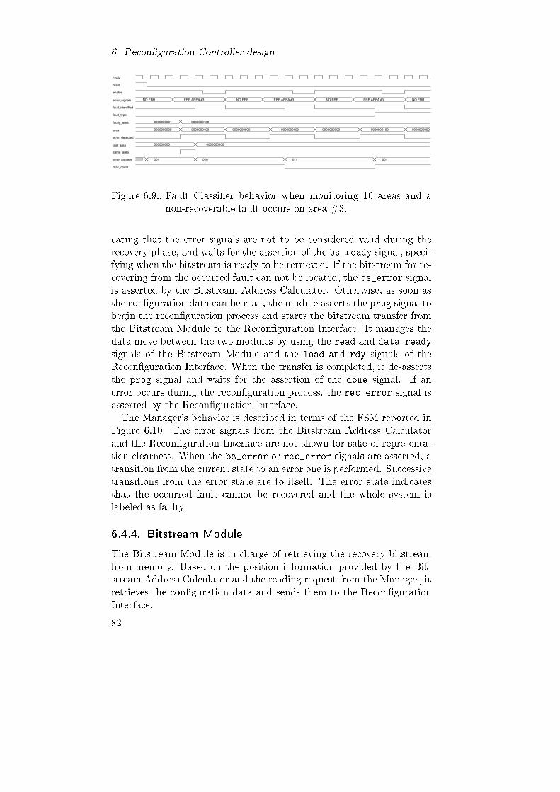
6. Recon�guration Controller design
clock
reset
enable
error_signals
fault_identified
fault_type
faulty_area
area
error_detected
last_area
same_area
error_counter
max_count
NO ERR NO ERR NO ERR NO ERRERR AREA #3 ERR AREA #3 ERR AREA #3
0000000100
0000000000 0000000100 0000000000 0000000100 0000000000 0000000100 0000000000
0000000100
001 010 011 001
0000000001
0000000001
Figure 6.9.: Fault Classi�er behavior when monitoring 10 areas and anon-recoverable fault occurs on area #3.
cating that the error signals are not to be considered valid during therecovery phase, and waits for the assertion of the bs_ready signal, speci-fying when the bitstream is ready to be retrieved. If the bitstream for re-covering from the occurred fault can not be located, the bs_error signalis asserted by the Bitstream Address Calculator. Otherwise, as soon asthe con�guration data can be read, the module asserts the prog signal tobegin the recon�guration process and starts the bitstream transfer fromthe Bitstream Module to the Recon�guration Interface. It manages thedata move between the two modules by using the read and data_ready
signals of the Bitstream Module and the load and rdy signals of theRecon�guration Interface. When the transfer is completed, it de-assertsthe prog signal and waits for the assertion of the done signal. If anerror occurs during the recon�guration process, the rec_error signal isasserted by the Recon�guration Interface.The Manager's behavior is described in terms of the FSM reported in
Figure 6.10. The error signals from the Bitstream Address Calculatorand the Recon�guration Interface are not shown for sake of representa-tion clearness. When the bs_error or rec_error signals are asserted, atransition from the current state to an error one is performed. Successivetransitions from the error state are to itself. The error state indicatesthat the occurred fault cannot be recovered and the whole system islabeled as faulty.
6.4.4. Bitstream Module
The Bitstream Module is in charge of retrieving the recovery bitstreamfrom memory. Based on the position information provided by the Bit-stream Address Calculator and the reading request from the Manager, itretrieves the con�guration data and sends them to the Recon�gurationInterface.
82
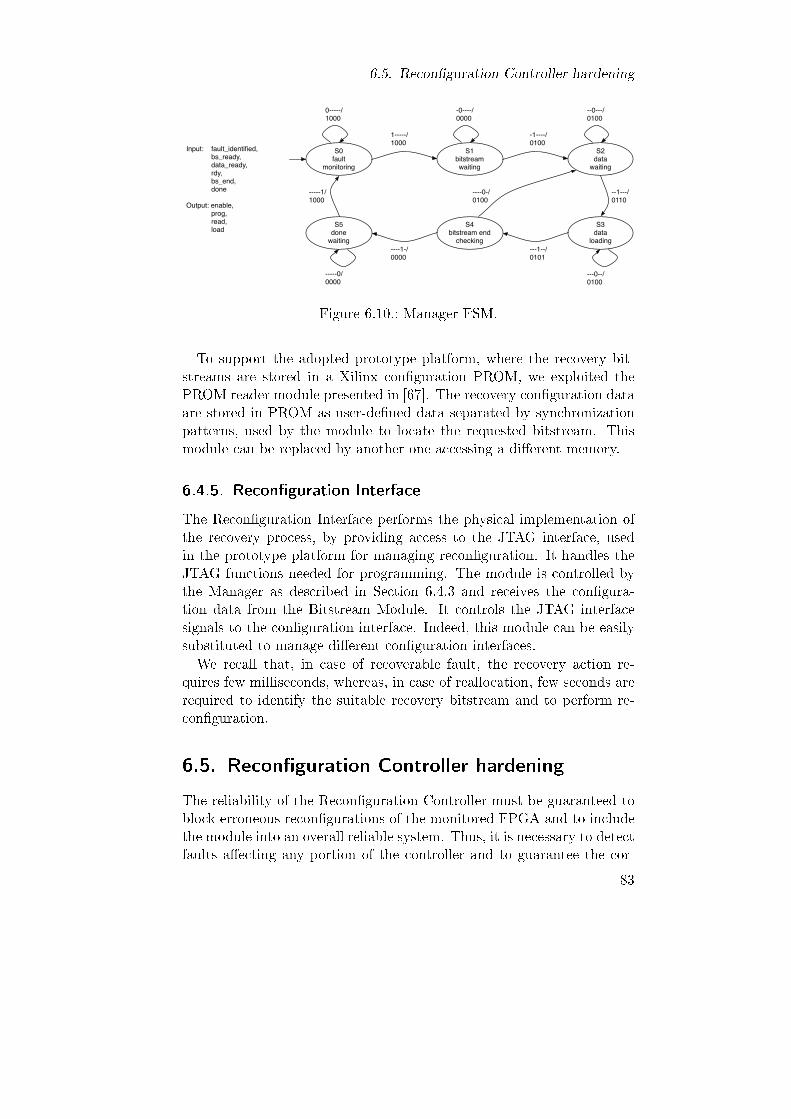
6.5. Recon�guration Controller hardening
Input: fault_identified, bs_ready, data_ready, rdy, bs_end, done
Output: enable, prog, read, load
S0fault
monitoring
S1bitstreamwaiting
S2data
waiting
S3data
loading
S4bitstream end
checking
S5done
waiting
0-----/1000
-0----/0000
--0---/0100
-----0/0000
---0--/0100
1-----/1000
-1----/0100
----1-/0000
---1--/0101
-----1/1000
--1---/0110
----0-/0100
Figure 6.10.: Manager FSM.
To support the adopted prototype platform, where the recovery bit-streams are stored in a Xilinx con�guration PROM, we exploited thePROM reader module presented in [67]. The recovery con�guration dataare stored in PROM as user-de�ned data separated by synchronizationpatterns, used by the module to locate the requested bitstream. Thismodule can be replaced by another one accessing a di�erent memory.
6.4.5. Recon�guration Interface
The Recon�guration Interface performs the physical implementation ofthe recovery process, by providing access to the JTAG interface, usedin the prototype platform for managing recon�guration. It handles theJTAG functions needed for programming. The module is controlled bythe Manager as described in Section 6.4.3 and receives the con�gura-tion data from the Bitstream Module. It controls the JTAG interfacesignals to the con�guration interface. Indeed, this module can be easilysubstituted to manage di�erent con�guration interfaces.We recall that, in case of recoverable fault, the recovery action re-
quires few milliseconds, whereas, in case of reallocation, few seconds arerequired to identify the suitable recovery bitstream and to perform re-con�guration.
6.5. Recon�guration Controller hardening
The reliability of the Recon�guration Controller must be guaranteed toblock erroneous recon�gurations of the monitored FPGA and to includethe module into an overall reliable system. Thus, it is necessary to detectfaults a�ecting any portion of the controller and to guarantee the cor-
83
6. Recon�guration Controller design
rectness of the recon�guration process. In the following, the hardeningof each component of the controller is analyzed and discussed. Particu-lar attention has been devoted to the Fault Classi�er, for which di�erenthardened implementations have been analyzed, for the criticality of theclassi�cation task.
6.5.1. Fault Classi�er hardening
Fault detection is required for the Fault Classi�er and it can be con-sidered su�cient since the engine is able to work correctly even whenit is reset after recon�guration, because of the robustness of the algo-rithm's parameters. In fact, a single fault in any one of the parametersbeing used by the classi�cation algorithm can only slightly impact onthe overall process. Should a fault occur, it will be detected and a reset(and recon�guration) of the controller would only cause a minor delayin classifying a fault as not-recoverable. In case of recoverable faults,the most frequent ones, a loss of information has no negative e�ects.Otherwise, in the rare, worst case where a non-recoverable fault has oc-curred and has not been identi�ed yet as such in the payload system,when the Fault Classi�er is reset, the fault's observations required forcorrect fault classi�cation are at most 2K-1 instead of K (we recall thatK is the threshold for classifying a fault as non-recoverable). This isan acceptable value if considering that K assumes only small values andthe latency estimated for the fault-error relation, now reduced since thethreshold is increased, is high enough to give a wide margin for reduc-tion. Hence, even the most critical registers for discriminating betweenfaults, i.e., the ones related to the error_counter and the last_ira,when reset, do not compromise seriously the correctness of the classi-�cation. Therefore, we deemed su�cient to guarantee the detection offaults in this portion of the entire architecture. Nevertheless, for thesake of completeness, implementations achieving fault tolerance proper-ties have been investigated. In particular, our analysis took into accountthe following hardened solutions: i) an implementation that applies Du-plication With Comparison (DWC) on the module, ii) a Self-Checking(SC) implementation based on the application of error detection codes,iii) a Self-Checking implementation coupled with TMR applied to themost critical registers (SC+), and iv) an implementation where TMRis applied to the entire system with a �ne granularity, by following theapproach o�ered by Xilinx's TMRTool (X-TMR) [68].
84
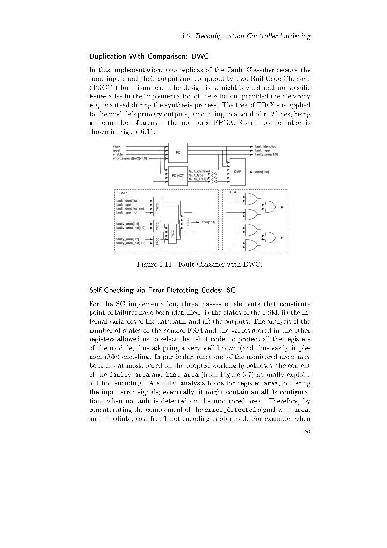
6.5. Recon�guration Controller hardening
Duplication With Comparison: DWC
In this implementation, two replicas of the Fault Classi�er receive thesame inputs and their outputs are compared by Two-Rail Code Checkers(TRCCs) for mismatch. The design is straightforward and no speci�cissues arise in the implementation of the solution, provided the hierarchyis guaranteed during the synthesis process. The tree of TRCCs is appliedto the module's primary outputs, amounting to a total of n+2 lines, beingn the number of areas in the monitored FPGA. Such implementation isshown in Figure 6.11.
FC
clockresetenableerror_signals[(nx2)-1:0]
fault_identifiedfault_typefaulty_area[3:0]
FC NOTCMPfault_identified
fault_typefaulty_area[3:0]
error[1:0]
fault_identifiedfault_typefault_identified_notfault_type_not
faulty_area[1:0]faulty_area_not[1:0]
faulty_area[3:2]faulty_area_not[3:2]
TRC
CTR
CC
TRC
C
TRC
C
TRC
C
error[1:0]
CMP TRCC
Figure 6.11.: Fault Classi�er with DWC.
Self-Checking via Error Detecting Codes: SC
For the SC implementation, three classes of elements that constitutepoint of failures have been identi�ed: i) the states of the FSM, ii) the in-ternal variables of the datapath, and iii) the outputs. The analysis of thenumber of states of the control FSM and the values stored in the otherregisters allowed us to select the 1-hot code, to protect all the registersof the module, thus adopting a very well known (and thus easily imple-mentable) encoding. In particular, since one of the monitored areas maybe faulty at most, based on the adopted working hypotheses, the contentof the faulty_area and last_area (from Figure 6.7) naturally exploitsa 1-hot encoding. A similar analysis holds for register area, bu�eringthe input error signals; eventually, it might contain an all 0s con�gura-tion, when no fault is detected on the monitored area. Therefore, byconcatenating the complement of the error_detected signal with area,an immediate, cost-free 1-hot encoding is obtained. For example, when
85

6. Recon�guration Controller design
monitoring 3 areas, if no fault is detected, the resulting code is 0001
since register area contains all 0s (no error is signalled) and the com-plement of error_detected is 1. On the other hand, the content ofthe register is 0010, 0100 or 1000 when area #1, #2 or #3 is detectedas faulty, respectively. Therefore, the 1-hot code is a natural choice forthe speci�c register. For the other internal variables (state register anderror_counter), since the number of states is limited, the code is not tooexpensive (the typical limitation of this code). The primary outputs aresingle lines (fault_identified and fault_type), encoded with a Two-Rail Code, whereas faulty_area is the encoded content of the register.The adoption of this code is particularly interesting, especially since thecode is usually recognized and supported also by automatic synthesistools, which usually have very little open con�guration options, espe-cially when targeting FPGA platforms, where the designer's control ofthe �nal implementation is hard to achieve. The SC implementation ofthe Fault Classi�er is shown in Figure 6.12 and consists of the functionalmodule generating encoded data and the necessary 1-hot/TRC checkers.
fsm_edc
clockreset
enable
area
n
error_signals[(nx2)-1:0]
faul
ty_a
rea
last
_are
a
erro
r_co
unte
r
K
00..10K
K
1
erro
r_de
tect
ed
sam
e_ar
ea[1
:0]
fault_identified[0]
fault_type[0]
faulty_area[n-1:0]
max
_cou
nt[1
:0]
clk
rst
trcc
1 1
fault_identified[1]
fault_type[1]
chk 1hot
chk 1hot
chk 1hot
chk 1hot
chk 1hot trcc
trcc trcc trcc
trcc trcc
trcc
error[1:0]
chk 1hot
state[3:0]
trcc
>>
MU
X00..01
1 1
2n
Figure 6.12.: SC Fault Classi�er.
86
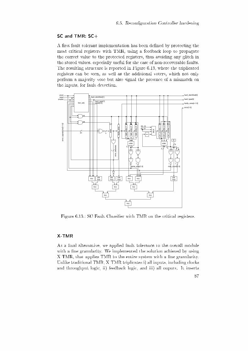
6.5. Recon�guration Controller hardening
SC and TMR: SC+
A �rst fault tolerant implementation has been de�ned by protecting themost critical registers with TMR, using a feedback loop to propagatethe correct value to the protected registers, thus avoiding any glitch inthe stored values, especially useful for the case of non-recoverable faults.The resulting structure is reported in Figure 6.13, where the triplicatedregisters can be seen, as well as the additional voters, which not onlyperform a majority vote but also signal the presence of a mismatch onthe inputs, for fault detection.
fsm_edc
clockreset
enable
area
n
error_signals[(nx2)-1:0]
faul
ty_a
rea
last
_are
a_1
err_
coun
ter_
1
K
K
1
erro
r_de
tect
ed
same_area[1:0]
fault_identified[0]
fault_type[0]
faulty_area[n-1:0]
max_count[1:0]
clk
rst
trcc
1 1
fault_identified[1]
fault_type[1]
chk 1hot
chk 1hot
trcc trcc trcc
trcc trcc
trcc
error[1:0]
chk 1hot
state[3:0]
last
_are
a_2
last
_are
a_3
voter
n
err_
coun
ter_
2
err_
coun
ter_
3
voter
trcc
22 K
trcc chk 1hot
00..10
>>
MU
X00..01
11
2n
Figure 6.13.: SC Fault Classi�er with TMR on the critical registers.
X-TMR
As a �nal alternative, we applied fault tolerance to the overall modulewith a �ne granularity. We implemented the solution achieved by usingX-TMR, that applies TMR to the entire system with a �ne granularity.Unlike traditional TMR, X-TMR triplicates i) all inputs, including clocksand throughput logic, ii) feedback logic, and iii) all ouputs. It inserts
87

6. Recon�guration Controller design
majority voters on feedback paths, and minority voters on outputs to de-tect and disable incorrect output paths. Such solution is the one usuallyadopted for recon�gurable FPGAs in high-radiation environments.
Cost analysis
The proposed implementations are compared in Table 6.1 with respect totheir overheads, in terms of area occupation (number of used slices and�ip �ops). The selected device is a Xilinx Virtex-II XC2V1000. Eachimplementation has been analyzed by varying K and n as discussed inChapter 5, to derive a trend in the implementation costs.As expected, as the number of monitored areas n increases, the size
of the Fault Classi�er increases, in all nominal and hardened versions.The most expensive solution is the one obtained by using X-TMR, en-tailing overheads around 370%, as expected. For the other implementa-tions, the incidence of the fault detection/tolerance added functionalityis within the foreseen, typical bounds, keeping the �nal hardened im-plementation within acceptable costs, that is less than 2% of the entireFPGA resources. In particular, overheads range from 40% and about100%, based on the di�erent solutions, allowing the designer to selectthe solutions s/he deems more interesting.
Table 6.1.: Area occupation (slices and FFs � in parenthesis) of the FaultClassi�er implementations and related overhead.
Solution K=2 (n=15) K=3 (n=10) K=4 (n=5) K=5 (n=3)area occ. over. area occ. over. area occ. over. area occ. over.
Nominal 86 (52) - 60 (36) - 40 (22) - 29 (16) -DWC 176 (104) 105% 120 (72) 100% 81 (44) 102% 58 (32) 100%SC 120 (53) 40% 96 (39) 60% 57 (25) 42% 47 (20) 62%SC+ 133 (53) 55% 107 (39) 78% 67 (25) 67% 58 (20) 100%X-TMR 406 (201) 372% 283 (138) 372% 186 (81) 365% 141 (57) 386%
The SC implementation allows us to have a competitive solution,characterized by acceptable costs and bene�ts in terms of reliability.It has been compared to the nominal solution in Table 6.2, in termsof area occupation of the modules composing the Fault Classi�er (seeFigure 6.7). Not all modules entail an increment in cost, in particularerror_detected_module and the registers faulty_area and last_area,that do not require modi�cations in the SC version. Alternative solu-tions, with acceptable but higher costs, do not entail signi�cative bene�tsin terms of additional reliability.
88
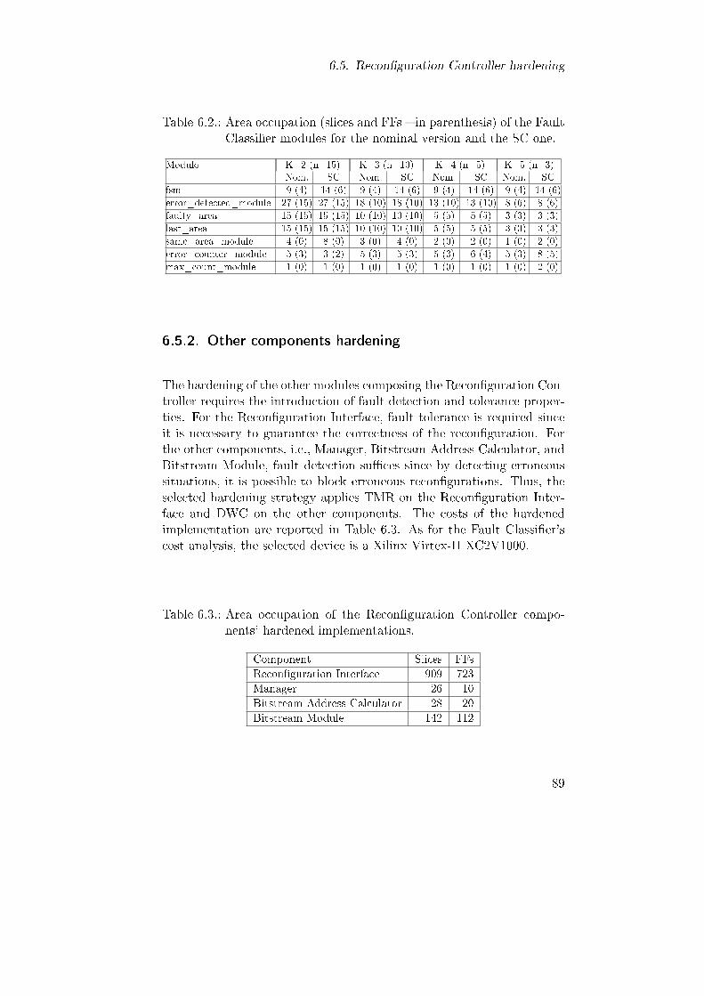
6.5. Recon�guration Controller hardening
Table 6.2.: Area occupation (slices and FFs � in parenthesis) of the FaultClassi�er modules for the nominal version and the SC one.
Module K=2 (n=15) K=3 (n=10) K=4 (n=5) K=5 (n=3)Nom. SC Nom. SC Nom. SC Nom. SC
fsm 9 (4) 14 (6) 9 (4) 14 (6) 9 (4) 14 (6) 9 (4) 14 (6)error_detected_module 27 (15) 27 (15) 18 (10) 18 (10) 13 (10) 13 (10) 8 (6) 8 (6)faulty_area 15 (15) 15 (15) 10 (10) 10 (10) 5 (5) 5 (5) 3 (3) 3 (3)last_area 15 (15) 15 (15) 10 (10) 10 (10) 5 (5) 5 (5) 3 (3) 3 (3)same_area_module 4 (0) 8 (0) 3 (0) 4 (0) 2 (0) 2 (0) 1 (0) 2 (0)error_counter_module 5 (3) 3 (2) 5 (3) 5 (3) 5 (3) 6 (4) 5 (3) 8 (5)max_count_module 1 (0) 1 (0) 1 (0) 1 (0) 1 (0) 1 (0) 1 (0) 2 (0)
6.5.2. Other components hardening
The hardening of the other modules composing the Recon�guration Con-troller requires the introduction of fault detection and tolerance proper-ties. For the Recon�guration Interface, fault tolerance is required sinceit is necessary to guarantee the correctness of the recon�guration. Forthe other components, i.e., Manager, Bitstream Address Calculator, andBitstream Module, fault detection su�ces since by detecting erroneoussituations, it is possible to block erroneous recon�gurations. Thus, theselected hardening strategy applies TMR on the Recon�guration Inter-face and DWC on the other components. The costs of the hardenedimplementation are reported in Table 6.3. As for the Fault Classi�er'scost analysis, the selected device is a Xilinx Virtex-II XC2V1000.
Table 6.3.: Area occupation of the Recon�guration Controller compo-nents' hardened implementations.
Component Slices FFsRecon�guration Interface 909 723Manager 26 10Bitstream Address Calculator 28 20Bitstream Module 142 112
89

6. Recon�guration Controller design
6.6. Chapter summary
The chapter has presented the design of the Recon�guration Controller,i.e., the module in charge of managing the fault recovery of the multi-FPGA platform. We introduced a controller performing the followingmain tasks: i) continuous check of the error signals from the monitoredFPGA, ii) classi�cation of fault into recoverable or non-recoverable, andiii) management of the recon�guration process to mitigate fault e�ects.Since the module will be hosted on an SRAM-based FPGA, it has beendesigned to be reliable itself, to prevent erroneous recon�gurations byidentifying an erroneous behavior of the controller as soon as it is ob-servable. A preliminary software implementation has been developed tore�ne the controller behavior. Due to the main limitations character-izing a software implementation, a hardware implementation has beenpreferred, and two reliability-aware solutions have been proposed.
90
7. Methodology evaluation
The reliability-aware design methodology presented in the thesis hasbeen evaluated by implementing a real case study. The design �ow de-scribed in Chapter 4 has been followed, and the developed prototypeframework has allowed to automate, as much as possible, the systemimplementation. Di�erent solutions have been explored, and the oneo�ering the most convenient trade-o� with respect to the designer's se-lected metrics has been identi�ed.The chapter is structured as follows: Section 7.1 describes the selected
case study and Sections from 7.2 to 7.5 present the experimental resultsfor the various tasks of the design �ow. Sections 7.6 and 7.7 compare theresults with the ones obtained by implementing an alternative version ofthe proposed design �ow and the �ow for �xed number of non-recoverablefaults, respectively. Finally, Section 7.8 draws the chapter summary.
7.1. Case study
The multi-FPGA platform selected for the evaluation of the design method-ology is a commercial board, a Synopsis HAPS-34 [25]. It is composedof four Xilinx FPGAs xc4vlx100, interconnected to each other in a meshtopology through connections for communication and con�guration. Fig-ure 7.1 shows the platform model, together with the parameters charac-terizing it. We recall that the platform model is composed of identicalFPGAs, di ∈ D, where D is the set of devices. Each FPGA is character-ized by the resources hosted on it, dev_resr, r ∈ R = {slice, bram,
dsp}, that is the number of resources in terms of slices, BRAMs, andDSPs, respectively. The FPGA is shaped as a grid of slices with columnsconstituted by di�erent types of resources. The inter-FPGA communi-cation is performed by dedicated wires; dev_wiresd1,d2 is the numberof wires between devices d1 and d2, and tot_wires is the number oftotal external wires on the platform. The platform topology is modeledby specifying the devices' adjacency and the communication paths be-tween non adjacent devices; direct_commd1,d2 equals to 1 if devices d1
and d2 are adjacent, 0 otherwise, and non_direct_commd1,d2,d3 equals to1 if device d1 allows the communication between devices d2 and d3, 0otherwise.
91

7. Methodology evaluation
FPGA 1xc4vlx100
FPGA 2xc4vlx100
FPGA 4xc4vlx100
FPGA 3xc4vlx100
Deviceʼs resources
dev_resslice 49152
dev_resbram 240
dev_resdsp 96
tot_wires 1756
non_direct_commi,j,k
i=1 1 2 3 4 i=2 1 2 3 4
1 0 0 0 0 1 0 0 1 0
2 0 0 0 0 2 0 0 0 0
3 0 0 0 0 3 0 0 0 0
4 0 1 0 0 4 0 0 0 0
i=3 1 2 3 4 i=4 1 2 3 4
1 0 0 0 0 1 0 0 0 0
2 0 0 0 1 2 0 0 0 0
3 0 0 0 0 3 1 0 0 0
4 0 0 0 0 4 0 0 0 0
dev_wiresi,j
i \ j 1 2 3 4
1 0 729 0 149
2 729 0 149 0
3 0 149 0 729
4 149 0 729 0
direct_commi,j
i \ j 1 2 3 4
1 0 1 0 1
2 1 0 1 0
3 0 1 0 1
4 1 0 1 0
Figure 7.1.: Multi-FPGA platform model.
The selected case study considers a circuit that performs image edgedetection, to be used by an overall control system for people/objectsrecognition. It detects the image edges and converts the image to transferit to di�erent devices. In a �rst phase, the edges are detected and over-lapped on the image. Then, the obtained raw bitmap image is encodedinto a JPEG compliant coded bitstream, selected as standard format.Finally, as color conversion is necessary when transferring data betweendevices that use di�erent color models, the image is converted to anothercolor system. In Figure 7.2(a), the nominal circuit structure is shown,annotated with the requirements <area_wiresa1,a2 , area_comma1,a2> forthe communication between modules; the throughput area_comma1,a2 isidenti�ed by the number of bits processed at a time. The resource re-quirements of the circuit are reported in Table 7.1, by considering theimplementation onto a Xilinx FPGA xc4vlx100 device. It is worth not-ing that a hardened implementation of the circuit, for example by meansof the classical TMR technique, could not be hosted onto a single FPGAfor lack of resources, hence multiple FPGAs should be exploited.
By considering the selected multi-FPGA platform and circuit, the pro-posed reliability-aware design �ow, shown in Figure 7.3, has been applied,as described in the following.
7.2. Preliminary partitioning
The circuit components have been distributed among the devices avail-able on the selected multi-FPGA platform.
We recall that the partitioning is a multi-objective problem, consider-ing as metrics the distribution uniformity and the minimization of theexternal communication both in terms of wires and throughput. The
92
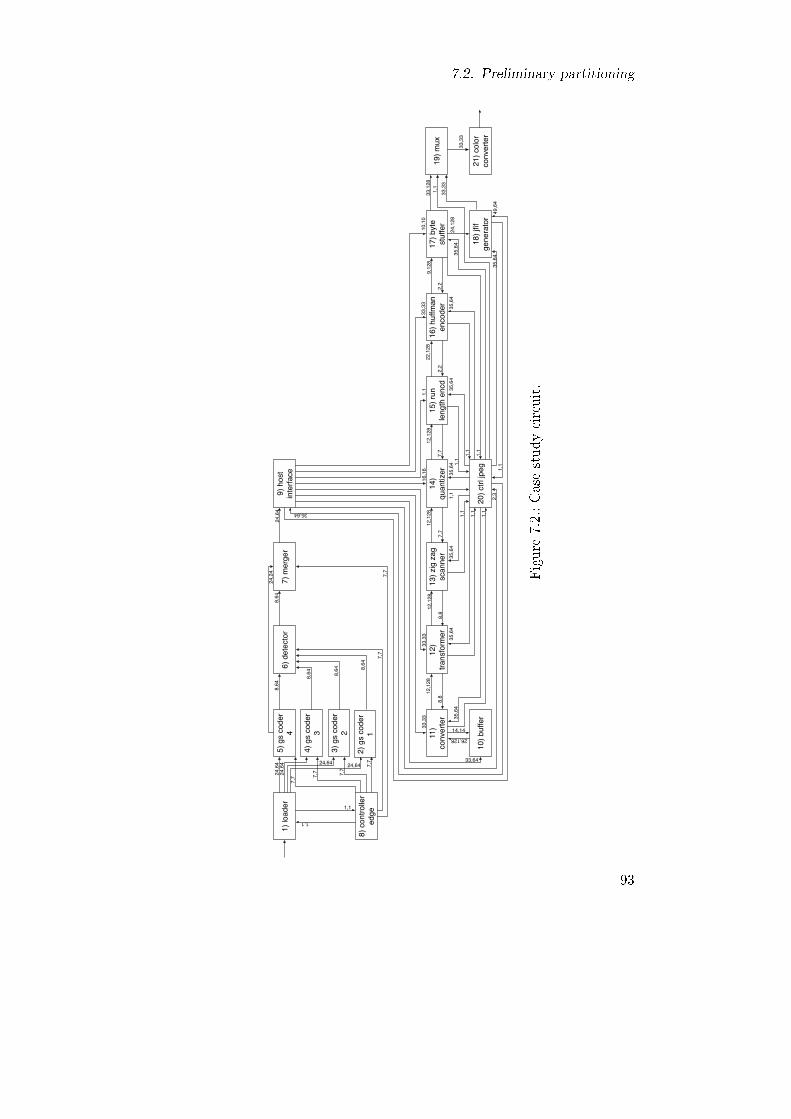
7.2. Preliminary partitioning
1) lo
ader
2) g
s co
der
1
3) g
s co
der
2
4) g
s co
der
3
5) g
s co
der
46)
det
ecto
r7)
mer
ger
8) c
ontro
ller
edge
9) h
ost
inte
rface
11)
conv
erte
r12
) tra
nsfo
rmer
13) z
ig z
ag
scan
ner
14)
quan
tizer
15) r
un
leng
th e
ncd
16) h
uffm
an
enco
der
17) b
yte
stuf
fer
19) m
ux
18) j
fif
gene
rato
r20
) ctrl
jpeg
10) b
uffe
r49
,64
35,64
2,3
33,64
33,3
333
,33
16,1
61,
133
,33
10,1
0
14,14
26,128
35,6
4
1,1
1,1
1,1
1,1
1,1
1,1
1,1
12,1
2812
,128
12,1
2812
,128
22,1
289,
128
33,1
28
8,8
8,8
7,7
7,7
2,2
2,2
35,6
435
,64
35,6
435
,64
35,6
435
,64
24,1
28
1,1
33,3
3
7,7
24,6
4
7,7
7,7
7,7
24,64 24,64
24,6
4
7,7
8,64
8,64
8,64
8,64
8,64
7,7
24,2
424
,64
1,1
1,1
1,1
35,6
4
21) c
olor
co
nver
ter
33,3
3
Figure7.2.:Casestudycircuit.
93
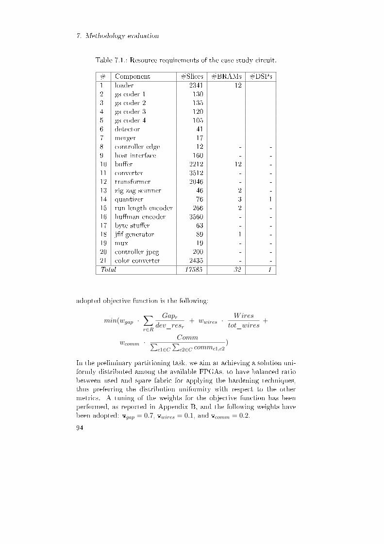
7. Methodology evaluation
Table 7.1.: Resource requirements of the case study circuit.
# Component #Slices #BRAMs #DSPs1 loader 2341 12 -2 gs coder 1 130 - -3 gs coder 2 135 - -4 gs coder 3 120 - -5 gs coder 4 105 - -6 detector 41 - -7 merger 17 - -8 controller edge 12 - -9 host interface 160 - -10 bu�er 2212 12 -11 converter 3512 - -12 transformer 2046 - -13 zig zag scanner 46 2 -14 quantizer 76 3 115 run length encoder 266 2 -16 hu�man encoder 3560 - -17 byte stu�er 63 - -18 j�f generator 89 1 -19 mux 19 - -20 controller jpeg 200 - -21 color converter 2435 - -Total 17585 32 1
adopted objective function is the following:
min(wgap ·∑r∈R
Gapr
dev_resr+ wwires · Wires
tot_wires+
wcomm · Comm∑c1∈C
∑c2∈C commc1,c2
)
In the preliminary partitioning task, we aim at achieving a solution uni-formly distributed among the available FPGAs, to have balanced ratiobetween used and spare fabric for applying the hardening techniques,thus preferring the distribution uniformity with respect to the othermetrics. A tuning of the weights for the objective function has beenperformed, as reported in Appendix B, and the following weights havebeen adopted: wgap = 0.7, wwires = 0.1, and wcomm = 0.2.
94
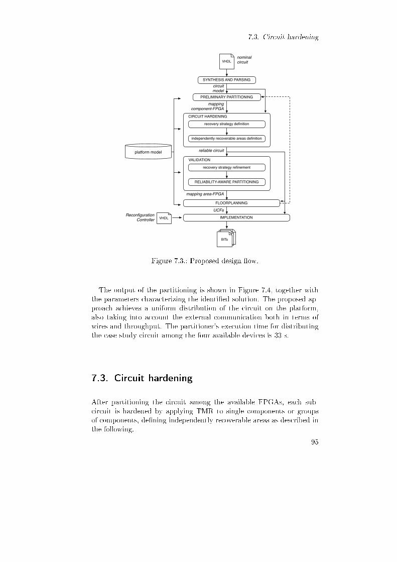
7.3. Circuit hardening
VHDLnominal circuit
RELIABILITY-AWARE PARTITIONING
FLOORPLANNING
BITs
platform model
circuitmodel
IMPLEMENTATIONVHDLReconfiguration
Controller
reliable circuit
UCFs
mapping area-FPGA
recovery strategy definition
CIRCUIT HARDENING
PRELIMINARY PARTITIONING
mapping component-FPGA
independently recoverable areas definition
recovery strategy refinement
SYNTHESIS AND PARSING
VALIDATION
Figure 7.3.: Proposed design �ow.
The output of the partitioning is shown in Figure 7.4, together withthe parameters characterizing the identi�ed solution. The proposed ap-proach achieves a uniform distribution of the circuit on the platform,also taking into account the external communication both in terms ofwires and throughput. The partitioner's execution time for distributingthe case study circuit among the four available devices is 33 s.
7.3. Circuit hardening
After partitioning the circuit among the available FPGAs, each sub-circuit is hardened by applying TMR to single components or groupsof components, de�ning independently recoverable areas as described inthe following.
95
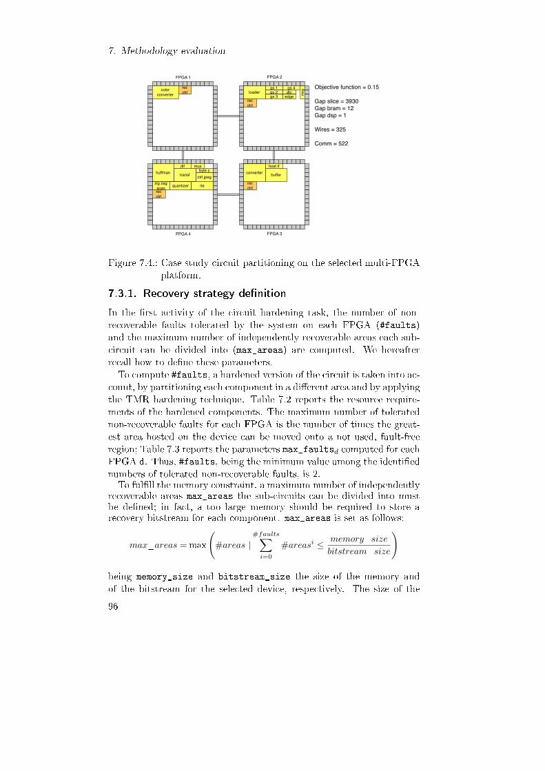
7. Methodology evaluation
Objective function = 0.15
Gap slice = 3930Gap bram = 12Gap dsp = 1
Wires = 325
Comm = 522
FPGA 1
FPGA 4
FPGA 2
FPGA 3
mrg
mux host ifbyte s
jfif
zig zag scan
ctrl jpeg
quantizer rle
dtcedge
gs 1gs 2gs 3
gs 4loader
huffman transf bufferconverter
color converter
rec ctrl
rec ctrl
rec ctrl
rec ctrl
Figure 7.4.: Case study circuit partitioning on the selected multi-FPGAplatform.
7.3.1. Recovery strategy de�nition
In the �rst activity of the circuit hardening task, the number of non-recoverable faults tolerated by the system on each FPGA (#faults)and the maximum number of independently recoverable areas each sub-circuit can be divided into (max_areas) are computed. We hereafterrecall how to de�ne these parameters.To compute #faults, a hardened version of the circuit is taken into ac-
count, by partitioning each component in a di�erent area and by applyingthe TMR hardening technique. Table 7.2 reports the resource require-ments of the hardened components. The maximum number of toleratednon-recoverable faults for each FPGA is the number of times the great-est area hosted on the device can be moved onto a not used, fault-freeregion; Table 7.3 reports the parameters max_faultsd computed for eachFPGA d. Thus, #faults, being the minimum value among the identi�ednumbers of tolerated non-recoverable faults, is 2.To ful�ll the memory constraint, a maximum number of independently
recoverable areas max_areas the sub-circuits can be divided into mustbe de�ned; in fact, a too large memory should be required to store arecovery bitstream for each component. max_areas is set as follows:
max_areas = max
(#areas |
#faults∑i=0
#areasi ≤ memory_size
bitstream_size
)
being memory_size and bitstream_size the size of the memory andof the bitstream for the selected device, respectively. The size of the
96

7.3. Circuit hardening
Table 7.2.: Resource requirements of the case study circuit's hardenedcomponents.
Component #Slices #BRAMs #DSPsloader 7411 36 -gs coder 1 422 - -gs coder 2 437 - -gs coder 3 392 - -gs coder 4 347 - -detector 155 - -merger 147 - -controller edge 220 - -host interface 1320 - -bu�er 6740 36 -converter 10640 - -transformer 6222 - -zig zag scanner 222 6 -quantizer 308 9 3run length encoder 918 6 -hu�man encoder 10728 - -byte stu�er 333 - -j�f generator 403 3 -mux 189 - -controller jpeg 1864 - -color converter 7437 - -Total 17585 32 1
Table 7.3.: De�nition of the parameters max_faultsd for each FPGA d.
Parameter FPGA 1 FPGA 2 FPGA 3 FPGA 4max_faultsd 5 5 2 2
97
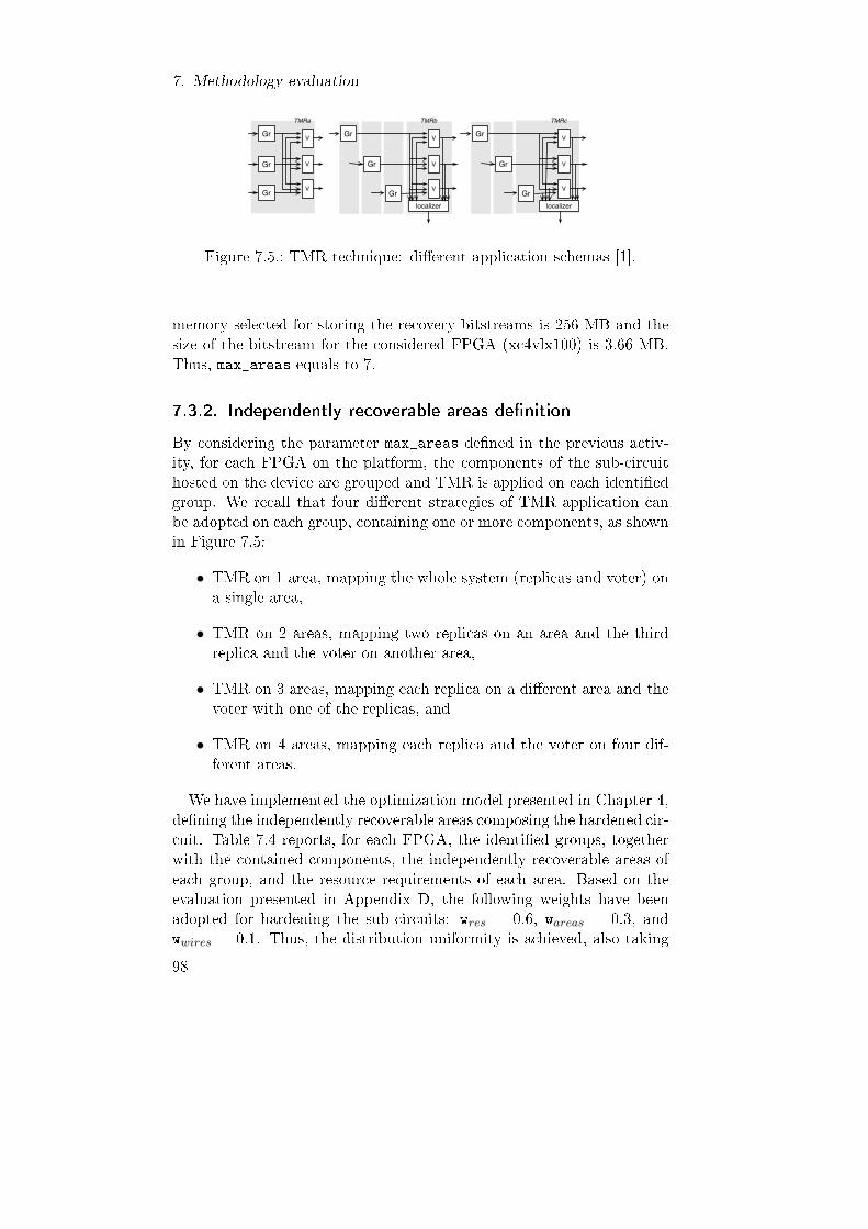
7. Methodology evaluation
TMRa
Gr
Gr
Gr
V
V
V
TMRb
Gr
Gr
Gr
V
V
V
TMRc
Gr
Gr
Gr
V
V
V
localizer localizer
Figure 7.5.: TMR technique: di�erent application schemas [1].
memory selected for storing the recovery bitstreams is 256 MB and thesize of the bitstream for the considered FPGA (xc4vlx100) is 3.66 MB.Thus, max_areas equals to 7.
7.3.2. Independently recoverable areas de�nition
By considering the parameter max_areas de�ned in the previous activ-ity, for each FPGA on the platform, the components of the sub-circuithosted on the device are grouped and TMR is applied on each identi�edgroup. We recall that four di�erent strategies of TMR application canbe adopted on each group, containing one or more components, as shownin Figure 7.5:
• TMR on 1 area, mapping the whole system (replicas and voter) ona single area,
• TMR on 2 areas, mapping two replicas on an area and the thirdreplica and the voter on another area,
• TMR on 3 areas, mapping each replica on a di�erent area and thevoter with one of the replicas, and
• TMR on 4 areas, mapping each replica and the voter on four dif-ferent areas.
We have implemented the optimization model presented in Chapter 4,de�ning the independently recoverable areas composing the hardened cir-cuit. Table 7.4 reports, for each FPGA, the identi�ed groups, togetherwith the contained components, the independently recoverable areas ofeach group, and the resource requirements of each area. Based on theevaluation presented in Appendix D, the following weights have beenadopted for hardening the sub-circuits: wres = 0.6, wareas = 0.3, andwwires = 0.1. Thus, the distribution uniformity is achieved, also taking
98
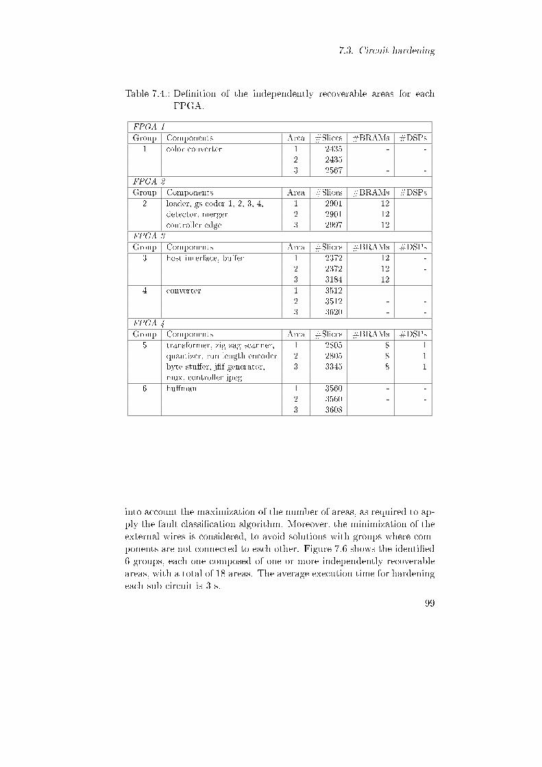
7.3. Circuit hardening
Table 7.4.: De�nition of the independently recoverable areas for eachFPGA.
FPGA 1
Group Components Area #Slices #BRAMs #DSPs1 color converter 1 2435 - -
2 2435 - -3 2567 - -
FPGA 2
Group Components Area #Slices #BRAMs #DSPs2 loader, gs coder 1, 2, 3, 4, 1 2901 12 -
detector, merger 2 2901 12controller edge 3 2997 12
FPGA 3
Group Components Area #Slices #BRAMs #DSPs3 host interface, bu�er 1 2372 12 -
2 2372 12 -3 3184 12 -
4 converter 1 3512 - -2 3512 - -3 3620 - -
FPGA 4
Group Components Area #Slices #BRAMs #DSPs5 transformer, zig zag scanner, 1 2805 8 1
quantizer, run length encoder 2 2805 8 1byte stu�er, j�f generator, 3 3345 8 1mux, controller jpeg
6 hu�man 1 3560 - -2 3560 - -3 3608 - -
into account the maximization of the number of areas, as required to ap-ply the fault classi�cation algorithm. Moreover, the minimization of theexternal wires is considered, to avoid solutions with groups where com-ponents are not connected to each other. Figure 7.6 shows the identi�ed6 groups, each one composed of one or more independently recoverableareas, with a total of 18 areas. The average execution time for hardeningeach sub-circuit is 3 s.
99
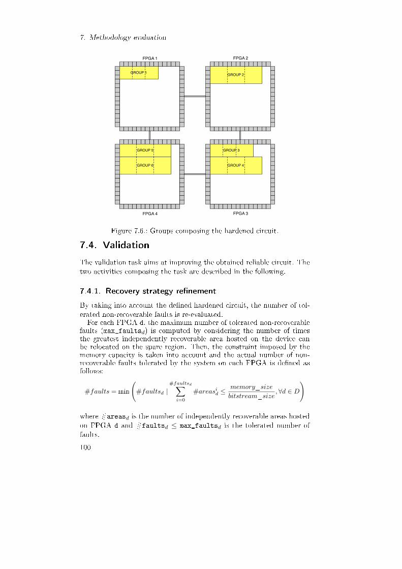
7. Methodology evaluation
FPGA 1
FPGA 4
FPGA 2
FPGA 3
GROUP 1 GROUP 2
GROUP 3
GROUP 4
GROUP 5
GROUP 6
Figure 7.6.: Groups composing the hardened circuit.
7.4. Validation
The validation task aims at improving the obtained reliable circuit. Thetwo activities composing the task are described in the following.
7.4.1. Recovery strategy re�nement
By taking into account the de�ned hardened circuit, the number of tol-erated non-recoverable faults is re-evaluated.For each FPGA d, the maximum number of tolerated non-recoverable
faults (max_faultsd) is computed by considering the number of timesthe greatest independently recoverable area hosted on the device canbe relocated on the spare region. Then, the constraint imposed by thememory capacity is taken into account and the actual number of non-recoverable faults tolerated by the system on each FPGA is de�ned asfollows:
#faults = min
(#faultsd |
#faultsd∑i=0
#areasid ≤
memory_size
bitstream_size,∀d ∈ D
)
where #areasd is the number of independently recoverable areas hostedon FPGA d and #faultsd ≤ max_faultsd is the tolerated number offaults.
100
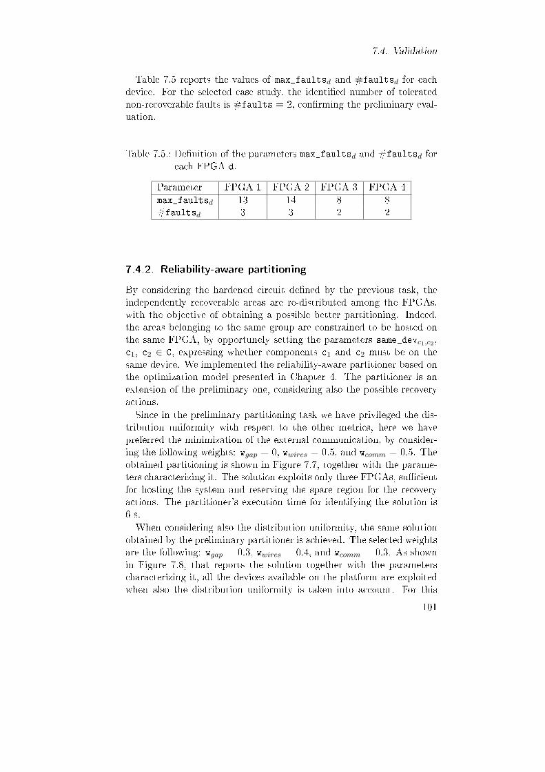
7.4. Validation
Table 7.5 reports the values of max_faultsd and #faultsd for eachdevice. For the selected case study, the identi�ed number of toleratednon-recoverable faults is #faults = 2, con�rming the preliminary eval-uation.
Table 7.5.: De�nition of the parameters max_faultsd and #faultsd foreach FPGA d.
Parameter FPGA 1 FPGA 2 FPGA 3 FPGA 4max_faultsd 13 14 8 8#faultsd 3 3 2 2
7.4.2. Reliability-aware partitioning
By considering the hardened circuit de�ned by the previous task, theindependently recoverable areas are re-distributed among the FPGAs,with the objective of obtaining a possible better partitioning. Indeed,the areas belonging to the same group are constrained to be hosted onthe same FPGA, by opportunely setting the parameters same_devc1,c2 ,c1, c2 ∈ C, expressing whether components c1 and c2 must be on thesame device. We implemented the reliability-aware partitioner based onthe optimization model presented in Chapter 4. The partitioner is anextension of the preliminary one, considering also the possible recoveryactions.Since in the preliminary partitioning task we have privileged the dis-
tribution uniformity with respect to the other metrics, here we havepreferred the minimization of the external communication, by consider-ing the following weights: wgap = 0, wwires = 0.5, and wcomm = 0.5. Theobtained partitioning is shown in Figure 7.7, together with the parame-ters characterizing it. The solution exploits only three FPGAs, su�cientfor hosting the system and reserving the spare region for the recoveryactions. The partitioner's execution time for identifying the solution is6 s.When considering also the distribution uniformity, the same solution
obtained by the preliminary partitioner is achieved. The selected weightsare the following: wgap = 0.3, wwires = 0.4, and wcomm = 0.3. As shownin Figure 7.8, that reports the solution together with the parameterscharacterizing it, all the devices available on the platform are exploitedwhen also the distribution uniformity is taken into account. For this
101

7. Methodology evaluation
Objective function = 0.06
Gap slice = 45495Gap bram = 84Gap dsp = 3
Wires = 59
Comm = 97
G1A1 G1A2 G1A3rec ctrl
rec ctrl
rec ctrl
G2A1 G2A2 G2A3
G3A1 G3A2 G3A3
G4A1 G4A2 G4A3
G5A1 G5A2 G5A3
G6A1 G6A2 G6A3
Figure 7.7.: Hardened circuit partitioning on the selected multi-FPGAplatform when privileging the minimization of the externalcommunication.
solution, taken into account for the subsequent step of the design �ow,the partitioner's execution time is 12 s.
Objective function = 0.38
Gap slice = 14328Gap bram = 60Gap dsp = 3
Wires = 234
Comm = 499
FPGA 1
FPGA 4
FPGA 2
FPGA 3
G1A1 G1A2 G1A3 G2A1 G2A2 G2A3
G5A3G5A2G5A1 G3A1 G3A2 G3A3
G4A1 G4A2 G4A3G6A1 G6A2 G6A3
rec ctrl
rec ctrl
rec ctrl
rec ctrl
Figure 7.8.: Hardened circuit partitioning on the selected multi-FPGAplatform when considering a trade-o� of the metrics.
102
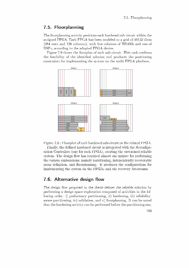
7.5. Floorplanning
7.5. Floorplanning
The �oorplanning activity positions each hardened sub-circuit within theassigned FPGA. Each FPGA has been modeled as a grid of 49152 slices(384 rows and 128 columns), with �ve columns of BRAMs and one ofDSPs, according to the adopted FPGA device.Figure 7.9 shows the �oorplan of each sub-circuit. This task con�rms
the feasibility of the identi�ed solution and produces the positioningconstraints for implementing the system on the multi-FPGA platform.
G1A1
G1A2
G1A3
G2A1
G2A2G2A3 G3A1
G4A1
G4A2G4A3
G5A1
G5A2G5A3
G6A1
G6A2G6A3
G7A1
G7A2G7A3
G8A1
FPGA 1
FPGA 4
FPGA 2
FPGA 3
rec ctrl
rec ctrl
rec
ctrl
rec
ctrl
Figure 7.9.: Floorplan of each hardened sub-circuit on the related FPGA.Finally, the de�ned hardened circuit is integrated with the Recon�gu-
ration Controllers (one for each FPGA), creating the envisioned reliablesystem. The design �ow has required almost one minute for performingthe various explorations, namely partitioning, independently recoverableareas de�nition, and �oorplanning. It produces the con�gurations forimplementing the system on the FPGAs and the recovery bitstreams.
7.6. Alternative design �ow
The design �ow proposed in the thesis de�nes the reliable solution byperforming a design space exploration composed of activities in the fol-lowing order: i) preliminary partitioning, ii) hardening, iii) reliability-aware partitioning, iv) validation, and v) �oorplanning. It can be notedthat the hardening activity can be performed before the partitioning one,
103

7. Methodology evaluation
thus an alternative design �ow can be considered. In this section, thealternative �ow shown in Figure 7.10 is implemented and the obtainedsolution is compared with the one of the proposed �ow.
VHDLnominal circuit
FLOORPLANNING
BITs
platform model
circuitmodel
IMPLEMENTATIONVHDLReconfiguration
Controller
reliable circuit
UCFs
CIRCUIT HARDENING
mapping area-FPGA
SYNTHESIS AND PARSING
PARTITIONING
RECOVERY STRATEGY EVALUATION
# non-rec faults
Figure 7.10.: Alternative design �ow.
The �rst activity of the alternative design space exploration performsthe hardening of the circuit. Since the proposed hardening optimizationmodel supports circuit with up to 10 components, as reported in Ap-pendix C, the circuit has been analyzed to reduce the number of compo-nents to be hardened. The preliminary grouping shown in Figure 7.11 hasbeen identi�ed, based on the components' resource requirement and in-terconnections. A minimum number of 12 areas is required, by consider-ing a minimum of 3 areas for each FPGA to apply the fault classi�cationalgorithm. The hardening activity has been performed by adopting thefollowing weights for the objective function of the optimization model:wres = 0.8, wareas = 0, and wwires = 0.2; the distribution uniformity isachieved, also taking into account the minimization of the external wires.Table 7.6 reports the hardened groups identi�ed by the activity, togetherwith the contained components, the independently recoverable areas ofeach group, and the resource requirements of each area. The solution iscomposed of 6 groups, each one composed of 3 independently recoverableareas, with a total of 18 areas.The obtained hardened circuit has been distributed among the avail-
able FPGAs. We aimed at achieving distribution uniformity, that hasbeen preferred with respect to the other metrics, to have balanced ra-
104
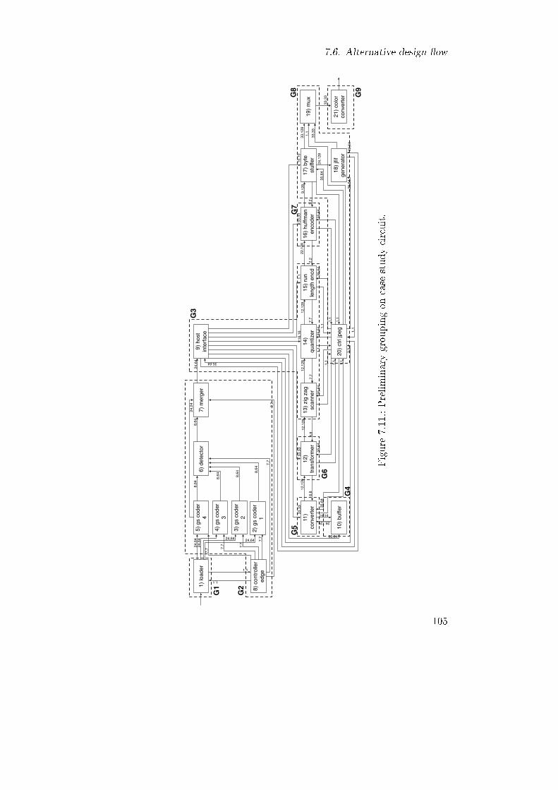
7.6. Alternative design �ow
1) lo
ader
2) g
s co
der
1
3) g
s co
der
2
4) g
s co
der
3
5) g
s co
der
46)
det
ecto
r7)
mer
ger
8) c
ontro
ller
edge
9) h
ost
inte
rface
11)
conv
erte
r12
) tra
nsfo
rmer
13) z
ig z
ag
scan
ner
14)
quan
tizer
15) r
un
leng
th e
ncd
16) h
uffm
an
enco
der
17) b
yte
stuf
fer
19) m
ux
18) j
fif
gene
rato
r20
) ctrl
jpeg
10) b
uffe
r49
,64
35,64
2,3
33,64
33,3
333
,33
16,1
61,
133
,33
10,1
0
14,14
26,128
35,6
4
1,1
1,1
1,1
1,1
1,1
1,1
1,1
12,1
2812
,128
12,1
2812
,128
22,1
289,
128
33,1
28
8,8
8,8
7,7
7,7
2,2
2,2
35,6
435
,64
35,6
435
,64
35,6
435
,64
24,1
28
1,1
33,3
3
7,7
24,6
4
7,7
7,7
7,7
24,64 24,64
24,6
4
7,7
8,64
8,64
8,64
8,64
8,64
7,7
24,2
424
,64
1,1
1,1
1,1
35,6
4
21) c
olor
co
nver
ter
33,3
3
G1
G2
G3
G4
G5
G6
G7
G8
G9
Figure7.11.:Prelim
inarygrouping
oncase
studycircuit.
105
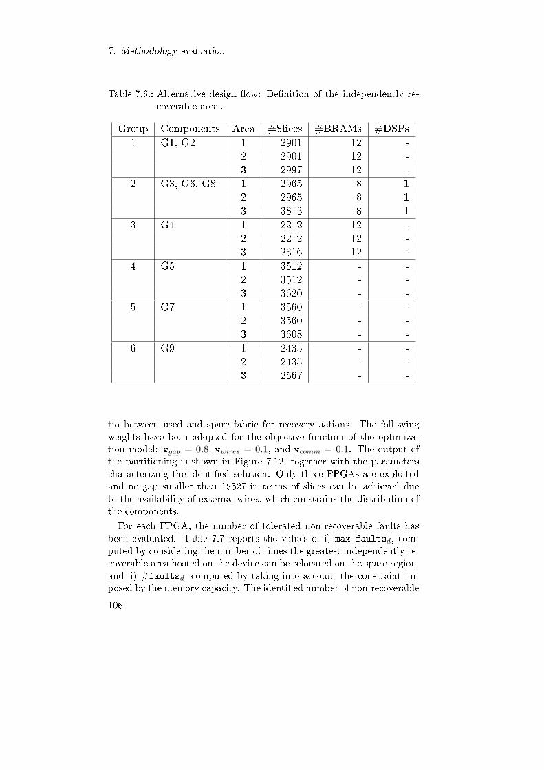
7. Methodology evaluation
Table 7.6.: Alternative design �ow: De�nition of the independently re-coverable areas.
Group Components Area #Slices #BRAMs #DSPs1 G1, G2 1 2901 12 -
2 2901 12 -3 2997 12 -
2 G3, G6, G8 1 2965 8 12 2965 8 13 3813 8 1
3 G4 1 2212 12 -2 2212 12 -3 2316 12 -
4 G5 1 3512 - -2 3512 - -3 3620 - -
5 G7 1 3560 - -2 3560 - -3 3608 - -
6 G9 1 2435 - -2 2435 - -3 2567 - -
tio between used and spare fabric for recovery actions. The followingweights have been adopted for the objective function of the optimiza-tion model: wgap = 0.8, wwires = 0.1, and wcomm = 0.1. The output ofthe partitioning is shown in Figure 7.12, together with the parameterscharacterizing the identi�ed solution. Only three FPGAs are exploitedand no gap smaller than 19527 in terms of slices can be achieved dueto the availability of external wires, which constrains the distribution ofthe components.
For each FPGA, the number of tolerated non-recoverable faults hasbeen evaluated. Table 7.7 reports the values of i) max_faultsd, com-puted by considering the number of times the greatest independently re-coverable area hosted on the device can be relocated on the spare region,and ii) #faultsd, computed by taking into account the constraint im-posed by the memory capacity. The identi�ed number of non-recoverable
106
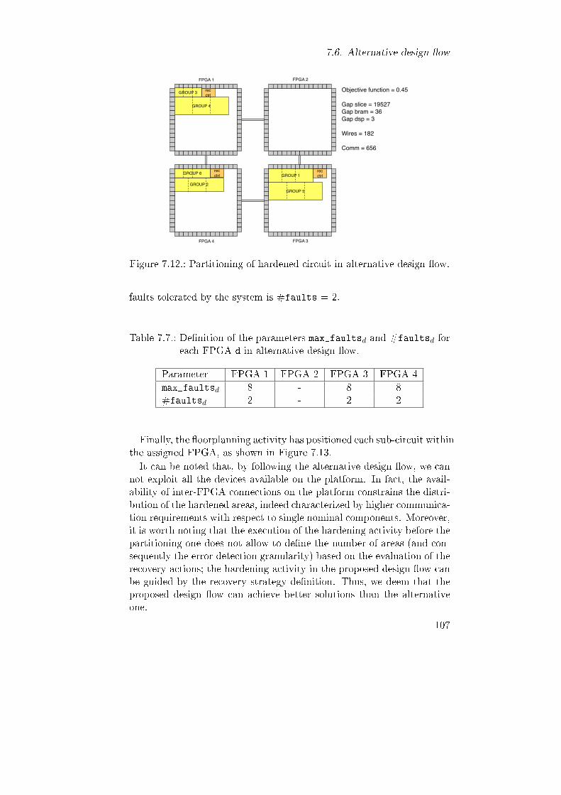
7.6. Alternative design �ow
Objective function = 0.45
Gap slice = 19527Gap bram = 36Gap dsp = 3
Wires = 182
Comm = 656
FPGA 1
FPGA 4
FPGA 2
FPGA 3
rec ctrl
GROUP 1
GROUP 2GROUP 5
GROUP 3
GROUP 4
GROUP 6 rec ctrl
rec ctrl
Figure 7.12.: Partitioning of hardened circuit in alternative design �ow.
faults tolerated by the system is #faults = 2.
Table 7.7.: De�nition of the parameters max_faultsd and #faultsd foreach FPGA d in alternative design �ow.
Parameter FPGA 1 FPGA 2 FPGA 3 FPGA 4max_faultsd 8 - 8 8#faultsd 2 - 2 2
Finally, the �oorplanning activity has positioned each sub-circuit withinthe assigned FPGA, as shown in Figure 7.13.It can be noted that, by following the alternative design �ow, we can
not exploit all the devices available on the platform. In fact, the avail-ability of inter-FPGA connections on the platform constrains the distri-bution of the hardened areas, indeed characterized by higher communica-tion requirements with respect to single nominal components. Moreover,it is worth noting that the execution of the hardening activity before thepartitioning one does not allow to de�ne the number of areas (and con-sequently the error detection granularity) based on the evaluation of therecovery actions; the hardening activity in the proposed design �ow canbe guided by the recovery strategy de�nition. Thus, we deem that theproposed design �ow can achieve better solutions than the alternativeone.
107

7. Methodology evaluation
FPGA 1
FPGA 4
FPGA 2
FPGA 3
G3A1G3A2
G3A3G4A1
G4A2G4A3
rec
ctrl
G2A1
G2A2
G2A3
G6A1
G6A2
G6A3
rec ctrl
G1A1
G1A2G1A3
G5A1
G5A2G5A3
rec
ctrl
Figure 7.13.: Floorplan of each hardened sub-circuit on the relatedFPGA in alternative design �ow.
7.7. Design �ow for �xed number of
non-recoverable faults
Throughout this chapter, the proposed design methodology has beenevaluated by building the envisioned fault tolerant system on a multi-FPGA platform speci�ed by the designer. Alternatively, it is possibleto de�ne the reliable system based on the number of non-recoverablefaults to be tolerated, by following the design �ow shown in Figure 7.14.In this section, we follow this alternative �ow, by considering two non-recoverable faults to be tolerated on each FPGA.
The circuit components are taken in input by the reliability-awareiterative partitioning task, that distributes them among the necessaryFPGAs. We recall that the partitioner takes into account a hardenedversion of the circuit, where TMR is applied at component-level, and,by starting from two FPGAs, increases the number of required devicesas far as it identi�es the suitable spare region for tolerating the non-recoverable faults. The partitioning of the selected case study is shownin Figure 7.15. Two FPGAs are su�cient to tolerate two non-recoverablefaults on each device.
108

7.8. Chapter summary
VHDLnominal circuit
RELIABILITY-AWARE PARTITIONING
FLOORPLANNING
BITs
device model
circuitmodel
IMPLEMENTATIONVHDLReconfiguration
Controller
reliable circuit
UCFs
mapping area-FPGA
recovery strategy definition
CIRCUIT HARDENING
RELIABILITY-AWARE ITERATIVE PARTITIONING
mapping component-FPGA
independently recoverable areas definition
recovery strategy refinement
SYNTHESIS AND PARSING
VALIDATION# non-rec faults
+
Figure 7.14.: Design �ow for �xed number of non-recoverable faults.
7.8. Chapter summary
In this chapter, we have evaluated the reliability-aware design method-ology presented in the thesis by implementing a real case study onto acommercial multi-FPGA platform. The design �ow introduced in Chap-ter 4 has been followed, and the developed prototype framework hasallowed to automate, as much as possible, the system implementation.Di�erent solutions have been explored and compared, by opportunelysetting the parameters of the exploited optimization models. The per-formed experimental session has allowed to evaluate and re�ne each taskof the �ow, in particular by tuning and analyzing the parameters. Theexperimental results, reported for each task, show that the proposedmethodology identi�es a reliable solution o�ering the most convenienttrade-o� with respect to the designer's selected metrics.
109
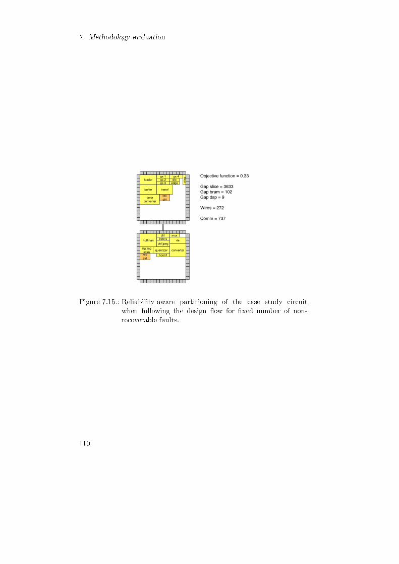
7. Methodology evaluation
Objective function = 0.33
Gap slice = 3633Gap bram = 102Gap dsp = 9
Wires = 272
Comm = 737
mrg
mux
host if
byte sjfif
zig zag scan
ctrl jpeg
quantizer
rle
dtcedge
gs 1gs 2gs 3
gs 4loader
huffman
transfbuffer
converter
color converter
rec ctrl
rec ctrl
Figure 7.15.: Reliability-aware partitioning of the case study circuitwhen following the design �ow for �xed number of non-recoverable faults.
110
8. Conclusions and future
research directions
The research presented in this thesis has proposed a complete method-ology for the design of reliable embedded systems on multi-FPGA plat-forms. The �nal aim of the work has been the exploitation of commercialSRAM-based FPGAs for mission-critical applications for systems of con-siderable size, requiring the use of more than a single FPGA device. Inparticular, we have considered space applications, characterized by strictreliability requirements due to the harsh environmental conditions andthe di�culty of system maintenance.The proposed methodology leads the designer in the realization of
a multi-FPGA system able to detect and cope with the occurrence offaults globally and autonomously, thus extending its lifetime and avail-ability. A circuit hardening approach based on a hybrid strategy hasbeen adopted; the circuit is hardened by means of traditional reliabil-ity techniques, e.g. exploiting space redundancy, and a recon�gurationof the FPGAs is used to mitigate fault e�ects. We have identi�ed twocategories of faults, based on the possibility to recover from them byrecon�guration: Recoverable faults, that can be mitigated by recon�gur-ing the system (and possibly only the faulty sub-system portion) withthe same con�guration used before fault occurrence, and non-recoverablefaults, that are caused by a destructive e�ect and lead to the necessity ofrelocating the functionality to a non-faulty region of the device. In theenvisioned reliable system, each FPGA hosts i) a hardened portion of theentire circuit, organized in independently recoverable areas that detect,mask/tolerate, and signal the occurrence of a fault, and ii) a Recon�g-uration Controller, in charge of monitoring the error signals and, whenneeded, performing the suitable recon�guration of the faulty part basedon the type of fault. The obtained autonomous fault tolerant system cancontinue working even if faults occur, thus increasing its lifetime. It isworth noting that the solution we pursue is not a generic one, rather itis identi�ed by means of a design space exploration, to evaluate di�erenttrade-o�s, meeting the designer's interests and constraints.The main innovative contributions provided by this thesis are summa-
rized as follows:
111
8. Conclusions and future research directions
• De�nition of a reliable multi-FPGA system with distributed controlarchitecture. Rather than making each FPGA an independent faulttolerant sub-system, able to locally detect and recover from faults,we have proposed a distributed solution, where each FPGA hosts ahardened portion of the system and a Recon�guration Controller.The aim is to achieve a higher level of reliability in the overall sys-tem, trying to avoid the single point of failure characterizing thecentralized solution, that needs to be implemented onto a particu-lar device (e.g., an ASIC or an antifuse-based FPGA).
• Management of both recoverable and non-recoverable faults. In lit-erature, only recoverable faults are usually targeted, whereas non-recoverable ones are rarely analyzed and taken into account. Thereliable system obtained by following the proposed methodology isable to discriminate between the two type of faults and cope withthem.
• Design of the Recon�guration Controller. We have proposed thedesign of the engine in charge of performing the envisioned faultclassi�cation and managing the recon�guration process. The re-liability of the Recon�guration Controller has been guaranteed toblock erroneous recon�gurations of the monitored FPGA and toinclude the module into the overall reliable system.
• De�nition of a complete �ow for designing autonomous fault tol-erant systems on multi-FPGA platforms. To our knowledge, inliterature there are no methodologies for the design of reliable sys-tems on multi-FPGA platforms. We introduced a complete �owfor designing such systems, and developed a prototype framework,by implementing the �ow and automating, as much as possible,the design, hardening, and implementation of the system.
The work that has been presented in this thesis is the �rst proposal ofa reliability-aware design methodology for embedded systems on multi-FPGA platforms. Thus, there are directions for future work aimed at itsimprovement and re�nement. They are summarized in the following.
• Experimental evaluation of the system reliability. A methodologicalevaluation of the proposed hardened system has been carried outand discussed. Nevertheless, an empirical evaluation can be per-formed by means of a fault injection campaign, to experimentallyanalyze the reliability achieved by the proposed system.
• System resynchronization after a recon�guration. In the thesis, theproblem of resynchronizing the system after recon�guration has
112
not been coped with. The approach is suitable for stateless ap-plications and it can be extended by implementing contributionsproposed in literature (e.g., [69]). A future work consists in investi-gating the resynchronization issue. In the �nal envisioned system,after realizing partial recon�guration to cope with the occurrenceof a recoverable fault, the recovered area is synchronized with thecorrect ones.
• De�nition of a reliable recon�guration protocol. Throughout thethesis, we have assumed that the recon�guration process is per-formed successfully. This is supported by the consideration thatrecon�guration is executed only on-demand, to cope with a de-tected error, hence, by taking into account a typical fault frequency,the occurrence of a new fault is unlikely. Nevertheless, for the sakeof system reliability, it is necessary to guarantee that when repro-gramming the device, either to recon�gure with the same bitstreamor to relocate a functionality, no new fault causes a problem leadingthe system into an unknown state.
• De�nition of recovery data storage. As stated in Chapter 4, a spe-ci�c recovery bitstream is required for each sequence of occurrednon-recoverable faults. Indeed, the number of bitstreams can bevery high also for tolerating few non-recoverable faults, hence tooa large memory should be required to store the con�guration data.Thus, strategies of data compression must be considered for mini-mizing the occupation of recovery bitstreams in memory.
Besides the identi�ed future directions, the proposed work can be re�nedby reviewing the design �ow to exploit lower level or runtime informationin the various steps.To conclude, this research has tackled several issues for the design of
reliable multi-FPGA systems, achieving the proposal of a whole method-ology. This has opened new research issues that can be pursued to re�nethe overall approach.
113


A. Partitioner performance
evaluation
This appendix reports the evaluation of the performance achieved by theproposed partitioning approach, presented in Chapter 4. We show that,despite being the partitioning problem NP-complete [49], our approach,based on Mixed Integer Linear Programming (MILP) optimization mod-els, runs in acceptable time. As described in Chapter 4, two models havebeen proposed, for the preliminary partitioning and for the reliability-aware one. Since the preliminary partitioner can be considered a simpli-�cation of the other one, not taking into account the possible recoveryactions, we hereafter consider the reliability-aware partitioner for theperformance evaluation.We recall that, to solve the optimization problems, we used the IBM
ILOG CPLEX 12.1 tool, which implements a parallel branch and cutprocedure [48]. The physical system supporting the partitioner executionis based on VMWare ESXi 4.0, running on an Intel Nehalem dual socketquad-core system with 32 GB of RAM. CPLEX is hosted on a VirtualMachine (VM) running Ubuntu 11.04 Linux. The VM has four physicalcores dedicated to its execution with guaranteed performance and 8GBof memory reserved.In order to show the partitioner's performance, an extensive exper-
imental analysis has been performed, by considering a large set of in-stances. The partitioner's parameters have been varied as shown in Ta-ble A.1. It is worth noting that same_deva1,a2 can take only values 0or 1, and the sum of the objective function's weights must equal to 1.Platforms with up to 8 devices connected in a mesh topology and char-acterized by the resources reported in Figure A.1, showing a SynopsisHAPS-34 commercial board [25], have been considered. Circuits includeup to 30 areas. The other parameters of the partitioner were randomlygenerated by assuming a uniform distribution in the reported intervals.In order to evaluate the performance of the proposed optimization
model, the average optimization time required for instances of variablesize is shown in Table A.2; each value reported in the table correspondsto the average time over 10 randomly generated instances. A total num-ber of 150 instances have been considered. For the most of the consid-
115
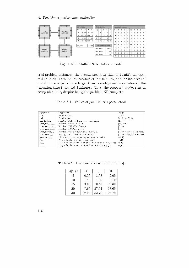
A. Partitioner performance evaluation
FPGA 1xc4vlx100
FPGA 2xc4vlx100
FPGA 4xc4vlx100
FPGA 3xc4vlx100
Deviceʼs resources
dev_resslice 49152
dev_resbram 240
dev_resdsp 96
tot_wires 1756
non_direct_commi,j,k
i=1 1 2 3 4 i=2 1 2 3 4
1 0 0 0 0 1 0 0 1 0
2 0 0 0 0 2 0 0 0 0
3 0 0 0 0 3 0 0 0 0
4 0 1 0 0 4 0 0 0 0
i=3 1 2 3 4 i=4 1 2 3 4
1 0 0 0 0 1 0 0 0 0
2 0 0 0 1 2 0 0 0 0
3 0 0 0 0 3 1 0 0 0
4 0 0 0 0 4 0 0 0 0
dev_wiresi,j
i \ j 1 2 3 4
1 0 729 0 149
2 729 0 149 0
3 0 149 0 729
4 149 0 729 0
direct_commi,j
i \ j 1 2 3 4
1 0 1 0 1
2 1 0 1 0
3 0 1 0 1
4 1 0 1 0
Figure A.1.: Multi-FPGA platform model.
ered problem instances, the overall execution time to identify the opti-mal solution is around few seconds or few minutes, and for instances ofmaximum size (which are larger than nowadays real applications), theexecution time is around 3 minutes. Thus, the proposed model runs inacceptable time, despite being the problem NP-complete.
Table A.1.: Values of partitioner's parameters.
Parameter Description Value|D| Set of devices 4, 6, 8|A| Set of areas 5, 10, 15, 20, 30num_faults Number of tolerated non-recoverable faults [1, 4]area_resa,r=slice Number of slices of area a [50, 2000]area_resa,r=bram Number of BRAMs of area a [0, 10]area_resa,r=dsp Number of DSPs of area a [0, 5]area_wiresai,aj Number of wires between areas ai and aj [0, 30] if i 6= j, 0 otherwisearea_commai,aj Throughput between areas ai and aj [0, 60] if i 6= j, 0 otherwisesame_devai,aj Placement of areas ai and aj on the same device {0, 1}wgap Weight for the distribution uniformity (0,1)wpins Weight for the minimization of the number of external wires (0,1)wcomm Weight for the minimization of the external throughput (0,1)
Table A.2.: Partitioner's execution times [s].
|A|\|D| 4 6 85 0.33 1.98 2.0010 1.49 4.46 9.1215 3.66 10.46 20.0020 7.63 27.01 67.6930 22.25 83.70 197.79
116
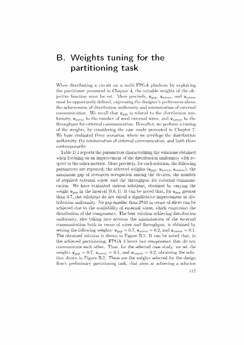
B. Weights tuning for the
partitioning task
When distributing a circuit on a multi-FPGA platform by exploitingthe partitioner presented in Chapter 4, the suitable weights of the ob-jective function must be set. More precisely, wgap, wwires, and wcomm
must be opportunely de�ned, expressing the designer's preferences aboutthe achievement of distribution uniformity and minimization of externalcommunication. We recall that wgap is related to the distribution uni-formity, wwires to the number of used external wires, and wcomm to thethroughput for external communication. Hereafter, we perform a tuningof the weights, by considering the case study presented in Chapter 7.We have evaluated three scenarios, where we privilege the distributionuniformity, the minimization of external communication, and both themcontemporarily.Table D.1 reports the parameters characterizing the solutions obtained
when focusing on an improvement of the distribution uniformity with re-spect to the other metrics. More precisely, for each solution, the followingparameters are reported; the selected weights (wgap, wwires, wcomm), themaximum gap of resources occupation among the devices, the numberof required external wires, and the throughput for external communi-cation. We have evaluated various solutions, obtained by varying theweight wgap in the interval [0.6, 1]. It can be noted that, for wgap greaterthan 0.7, the solutions do not entail a signi�cative improvement in dis-tribution uniformity. No gap smaller than 2840 in terms of slices can beachieved due to the availability of external wires, which constrains thedistribution of the components. The best solution achieving distributionuniformity, also taking into account the minimization of the externalcommunication both in terms of wires and throughput, is obtained bysetting the following weights: wgap = 0.7, wwires = 0.2, and wcomm = 0.1.The obtained solution is shown in Figure B.1. It can be noted that, inthe achieved partitioning, FPGA 4 hosts two components that do notcommunicate each other. Thus, for the selected case study, we set theweights wgap = 0.7, wwires = 0.1, and wcomm = 0.2, obtaining the solu-tion shown in Figure B.2. These are the weights selected for the design�ow's preliminary partitioning task, that aims at achieving a solution
117
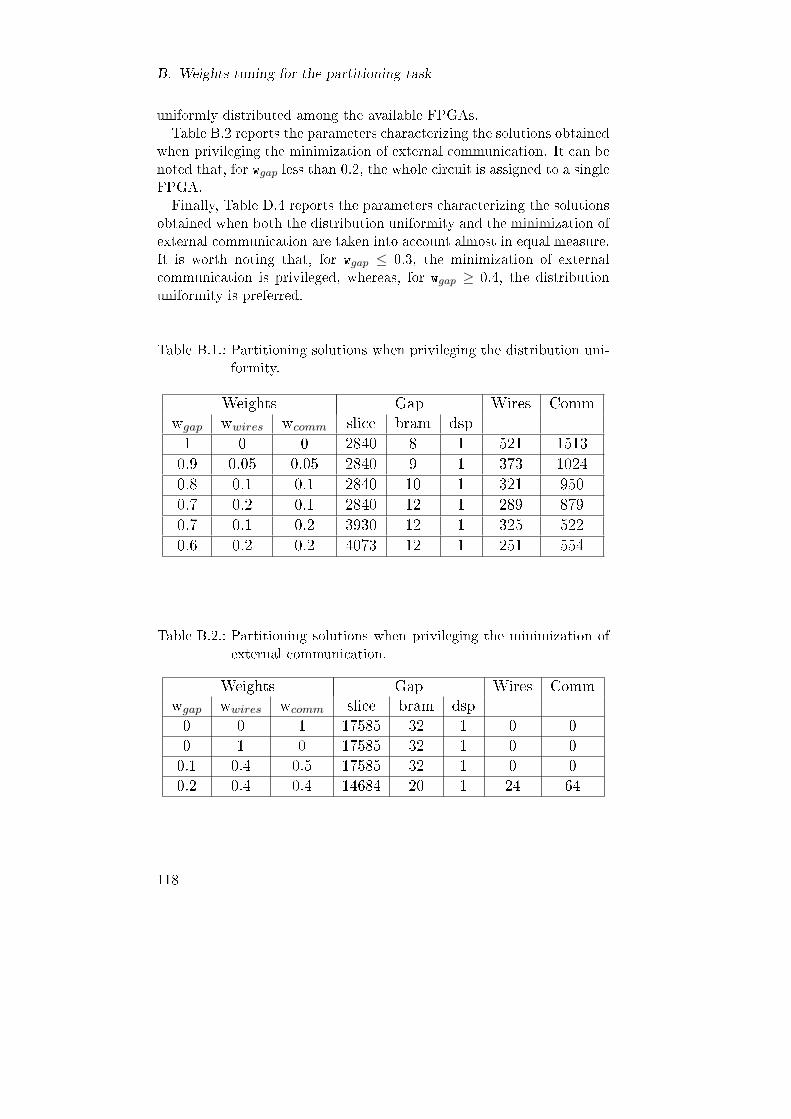
B. Weights tuning for the partitioning task
uniformly distributed among the available FPGAs.Table B.2 reports the parameters characterizing the solutions obtained
when privileging the minimization of external communication. It can benoted that, for wgap less than 0.2, the whole circuit is assigned to a singleFPGA.Finally, Table D.4 reports the parameters characterizing the solutions
obtained when both the distribution uniformity and the minimization ofexternal communication are taken into account almost in equal measure.It is worth noting that, for wgap ≤ 0.3, the minimization of externalcommunication is privileged, whereas, for wgap ≥ 0.4, the distributionuniformity is preferred.
Table B.1.: Partitioning solutions when privileging the distribution uni-formity.
Weights Gap Wires Commwgap wwires wcomm slice bram dsp1 0 0 2840 8 1 521 15130.9 0.05 0.05 2840 9 1 373 10240.8 0.1 0.1 2840 10 1 321 9500.7 0.2 0.1 2840 12 1 289 8790.7 0.1 0.2 3930 12 1 325 5220.6 0.2 0.2 4073 12 1 251 554
Table B.2.: Partitioning solutions when privileging the minimization ofexternal communication.
Weights Gap Wires Commwgap wwires wcomm slice bram dsp0 0 1 17585 32 1 0 00 1 0 17585 32 1 0 00.1 0.4 0.5 17585 32 1 0 00.2 0.4 0.4 14684 20 1 24 64
118

FPGA 1
FPGA 4
FPGA 2
FPGA 3
mrg
mux
host ifbyte s
jfif
zig zag scan
ctrl jpeg
quantizer rle
dtcedge
gs 1gs 2gs 3
gs 4loaderhuffman
transf
bufferconvertercolor
converter
Figure B.1.: Case study circuit partitioning on the selected multi-FPGAplatform by setting wgap = 0.7, wwires = 0.2, and wcomm =0.1.
Table B.3.: Partitioning solutions when considering both the distributionuniformity and the minimization of external communication.
Weights Gap Wires Commwgap wwires wcomm slice bram dsp0.3 0.4 0.3 14684 20 1 24 640.4 0.3 0.3 4073 12 1 251 5540.5 0.2 0.3 4073 12 1 251 5540.5 0.3 0.2 4073 12 1 251 554
119
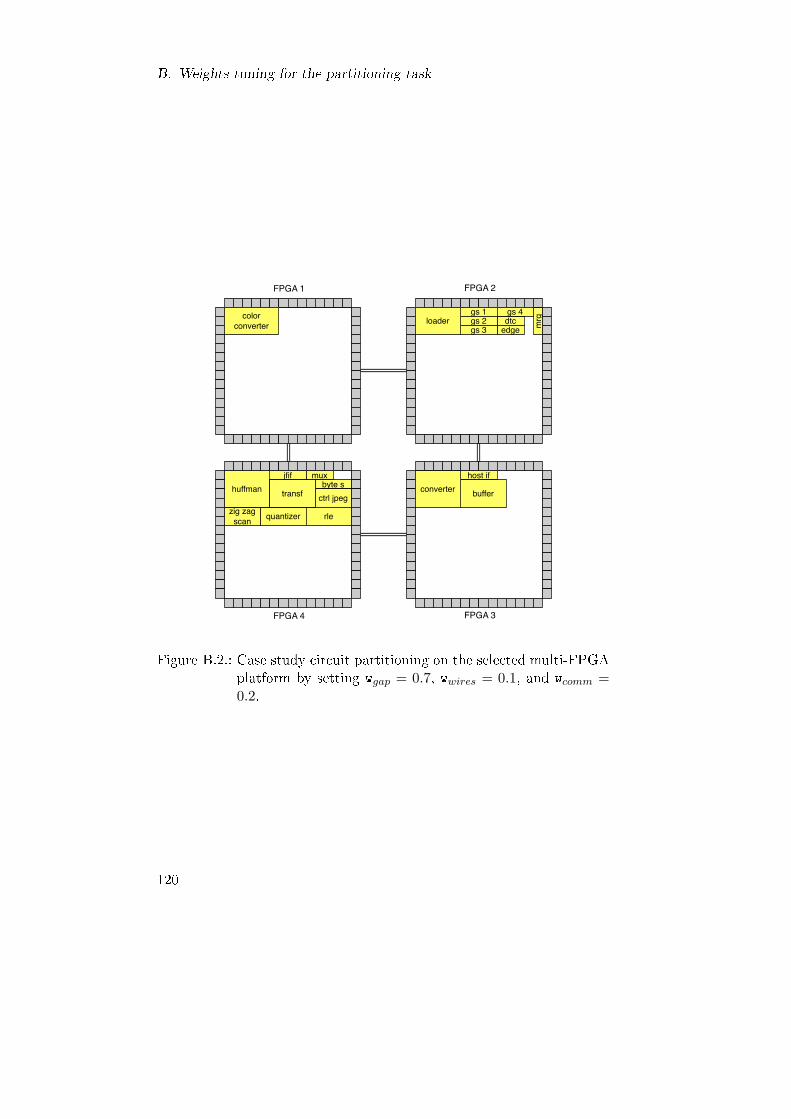
B. Weights tuning for the partitioning task
FPGA 1
FPGA 4
FPGA 2
FPGA 3
mrg
mux host ifbyte s
jfif
zig zag scan
ctrl jpeg
quantizer rle
dtcedge
gs 1gs 2gs 3
gs 4loader
huffman transf bufferconverter
color converter
Figure B.2.: Case study circuit partitioning on the selected multi-FPGAplatform by setting wgap = 0.7, wwires = 0.1, and wcomm =0.2.
120

C. Hardening approach
performance evaluation
This appendix reports the analysis of the performance achieved by theproposed hardening approach, presented in Chapter 4. The optimizationmodel's execution time has been evaluated by performing an extensiveexperimental analysis.We recall that, to solve the optimization problems, we used the IBM
ILOG CPLEX 12.1 tool, which implements a parallel branch and cutprocedure [48]. The physical system supporting the partitioner executionis based on VMWare ESXi 4.0, running on an Intel Nehalem dual socketquad-core system with 32 GB of RAM. CPLEX is hosted on a VirtualMachine (VM) running Ubuntu 11.04 Linux. The VM has four physicalcores dedicated to its execution with guaranteed performance and 8GBof memory reserved.The performed experimental analysis has considered various instances,
obtained by varying the model's parameters. Circuits with up to 15components have been taken into account. The components are assignedto groups, whose cardinality is the minimum between the number ofcomponents (|C|) and the number of areas the circuit can be dividedinto (max_areas). The parameter max_areas gets the following values:i) d|C|/2e, to consider an average case where the maximum number ofareas is less than the number of components, ii) |C|, when the number ofareas is equal to the number of components, and iii) |C| · 4, to considerthe worst case assigning each component to a group where TMR on 4areas is applied. The other parameters characterizing the circuit wererandomly generated by assuming a uniform distribution in the intervalsreported in Table C.1.In order to evaluate the performance of the proposed optimization
model, the average optimization time required for instances of variablesize is shown in Table C.2; each value reported in the table correspondsto the average time over 10 randomly generated instances. A total num-ber of 150 instances have been considered. When no execution time isreported, out-of-memory errors have occurred for one or more of the ran-dom instances. Thus, the proposed model is suitable when consideringcircuits with up to 10 components, characterizing most of nowadays ap-
121
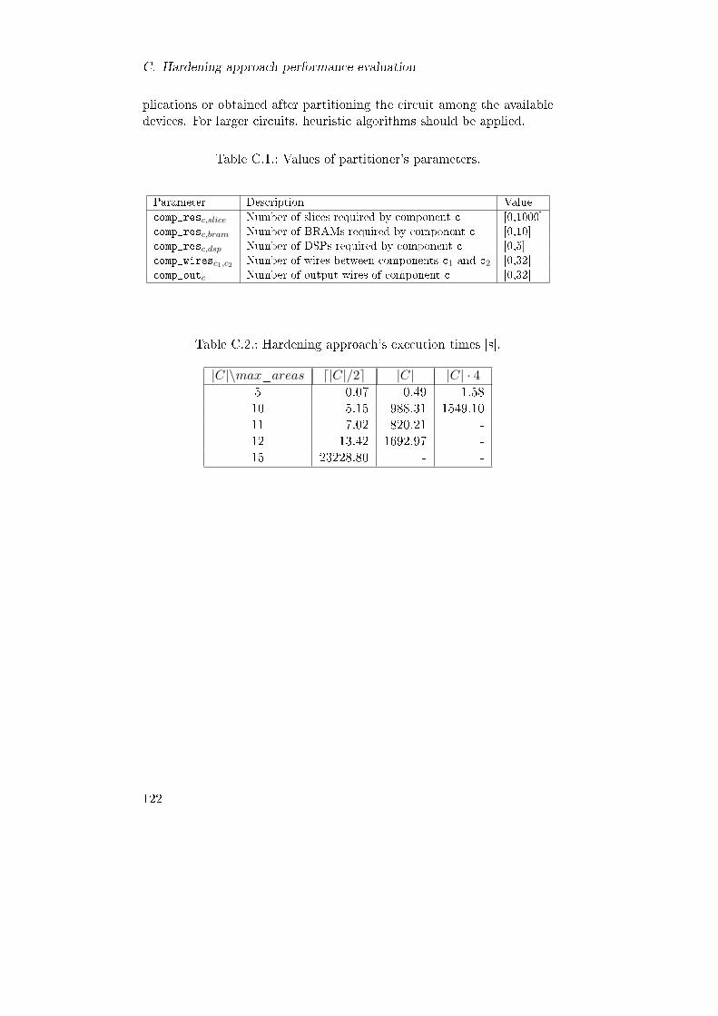
C. Hardening approach performance evaluation
plications or obtained after partitioning the circuit among the availabledevices. For larger circuits, heuristic algorithms should be applied.
Table C.1.: Values of partitioner's parameters.
Parameter Description Valuecomp_resc,slice Number of slices required by component c [0,1000]comp_resc,bram Number of BRAMs required by component c [0,10]comp_resc,dsp Number of DSPs required by component c [0,5]comp_wiresc1,c2 Number of wires between components c1 and c2 [0,32]comp_outc Number of output wires of component c [0,32]
Table C.2.: Hardening approach's execution times [s].
|C|\max_areas d|C|/2e |C| |C| · 45 0.07 0.49 1.5810 5.15 988.31 1549.1011 7.02 820.21 -12 13.42 1692.97 -15 23228.80 - -
122
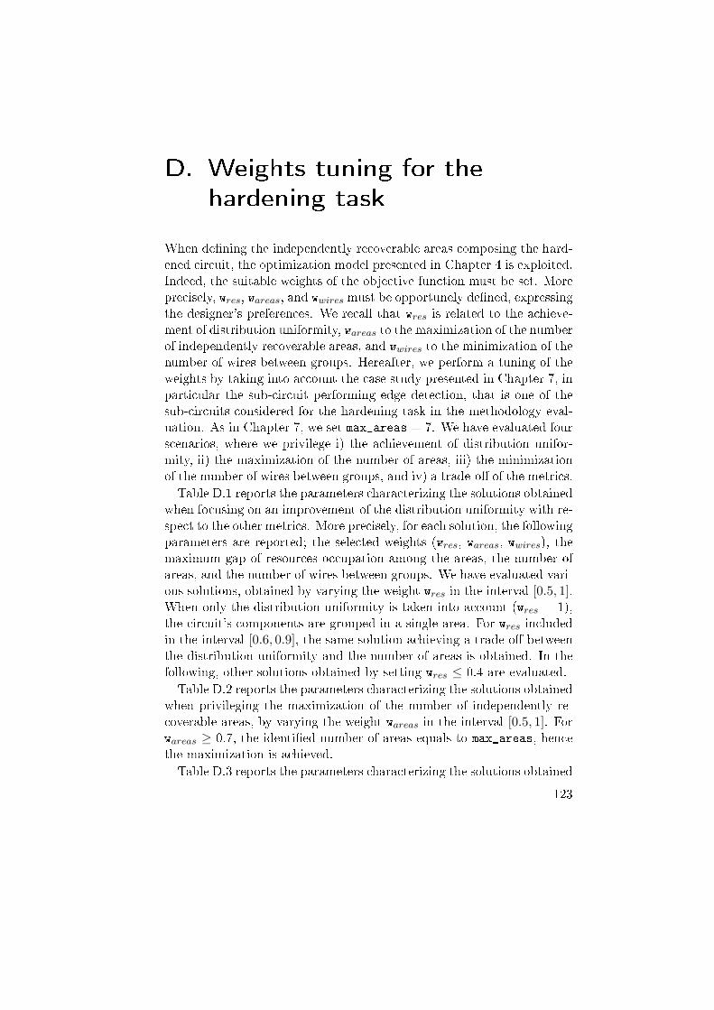
D. Weights tuning for the
hardening task
When de�ning the independently recoverable areas composing the hard-ened circuit, the optimization model presented in Chapter 4 is exploited.Indeed, the suitable weights of the objective function must be set. Moreprecisely, wres, wareas, and wwires must be opportunely de�ned, expressingthe designer's preferences. We recall that wres is related to the achieve-ment of distribution uniformity, wareas to the maximization of the numberof independently recoverable areas, and wwires to the minimization of thenumber of wires between groups. Hereafter, we perform a tuning of theweights by taking into account the case study presented in Chapter 7, inparticular the sub-circuit performing edge detection, that is one of thesub-circuits considered for the hardening task in the methodology eval-uation. As in Chapter 7, we set max_areas = 7. We have evaluated fourscenarios, where we privilege i) the achievement of distribution unifor-mity, ii) the maximization of the number of areas, iii) the minimizationof the number of wires between groups, and iv) a trade-o� of the metrics.Table D.1 reports the parameters characterizing the solutions obtained
when focusing on an improvement of the distribution uniformity with re-spect to the other metrics. More precisely, for each solution, the followingparameters are reported; the selected weights (wres, wareas, wwires), themaximum gap of resources occupation among the areas, the number ofareas, and the number of wires between groups. We have evaluated vari-ous solutions, obtained by varying the weight wres in the interval [0.5, 1].When only the distribution uniformity is taken into account (wres = 1),the circuit's components are grouped in a single area. For wres includedin the interval [0.6, 0.9], the same solution achieving a trade-o� betweenthe distribution uniformity and the number of areas is obtained. In thefollowing, other solutions obtained by setting wres ≤ 0.4 are evaluated.Table D.2 reports the parameters characterizing the solutions obtained
when privileging the maximization of the number of independently re-coverable areas, by varying the weight wareas in the interval [0.5, 1]. Forwareas ≥ 0.7, the identi�ed number of areas equals to max_areas, hencethe maximization is achieved.Table D.3 reports the parameters characterizing the solutions obtained
123
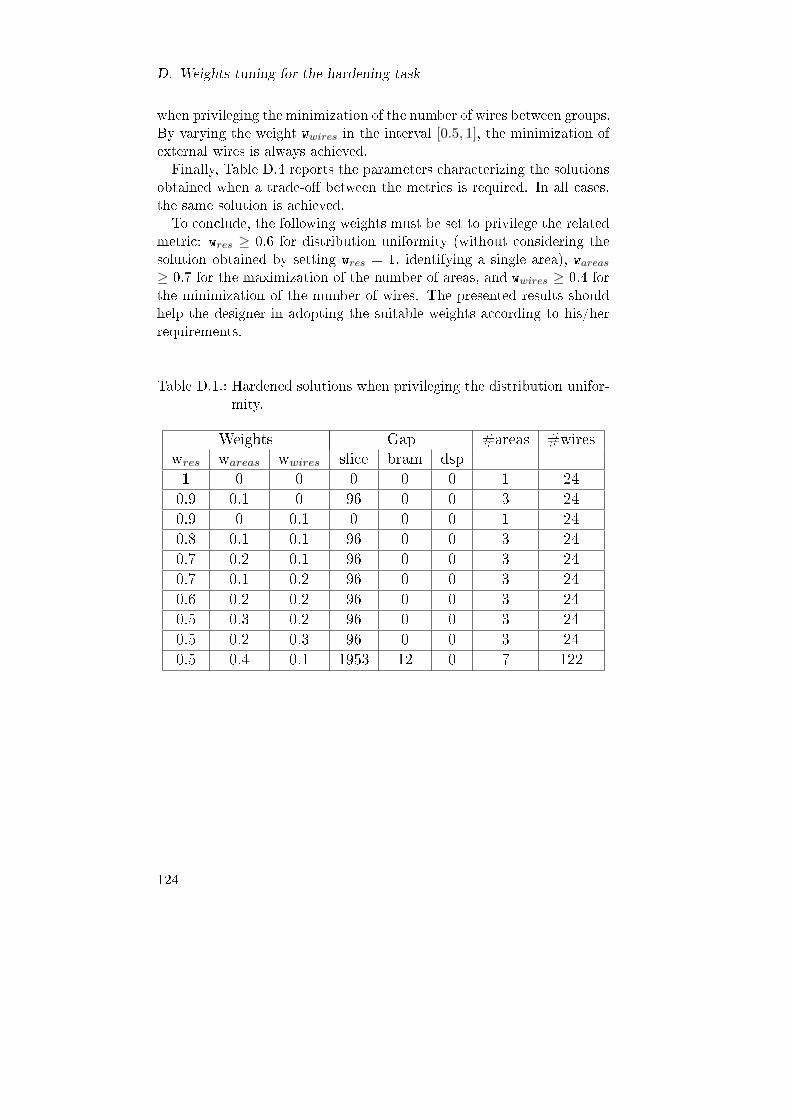
D. Weights tuning for the hardening task
when privileging the minimization of the number of wires between groups.By varying the weight wwires in the interval [0.5, 1], the minimization ofexternal wires is always achieved.Finally, Table D.4 reports the parameters characterizing the solutions
obtained when a trade-o� between the metrics is required. In all cases,the same solution is achieved.To conclude, the following weights must be set to privilege the related
metric: wres ≥ 0.6 for distribution uniformity (without considering thesolution obtained by setting wres = 1, identifying a single area), wareas
≥ 0.7 for the maximization of the number of areas, and wwires ≥ 0.4 forthe minimization of the number of wires. The presented results shouldhelp the designer in adopting the suitable weights according to his/herrequirements.
Table D.1.: Hardened solutions when privileging the distribution unifor-mity.
Weights Gap #areas #wireswres wareas wwires slice bram dsp1 0 0 0 0 0 1 240.9 0.1 0 96 0 0 3 240.9 0 0.1 0 0 0 1 240.8 0.1 0.1 96 0 0 3 240.7 0.2 0.1 96 0 0 3 240.7 0.1 0.2 96 0 0 3 240.6 0.2 0.2 96 0 0 3 240.5 0.3 0.2 96 0 0 3 240.5 0.2 0.3 96 0 0 3 240.5 0.4 0.1 1953 12 0 7 122
124
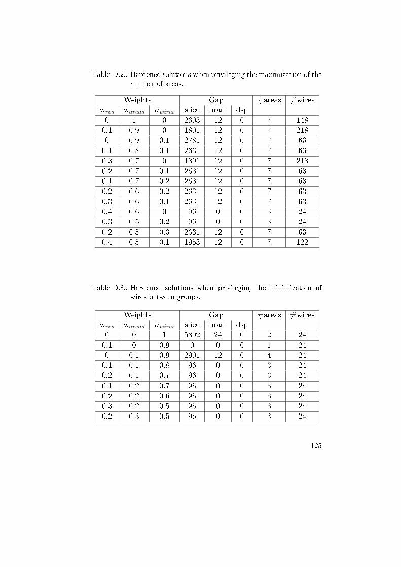
Table D.2.: Hardened solutions when privileging the maximization of thenumber of areas.
Weights Gap #areas #wireswres wareas wwires slice bram dsp0 1 0 2603 12 0 7 1480.1 0.9 0 1801 12 0 7 2180 0.9 0.1 2781 12 0 7 630.1 0.8 0.1 2631 12 0 7 630.3 0.7 0 1801 12 0 7 2180.2 0.7 0.1 2631 12 0 7 630.1 0.7 0.2 2631 12 0 7 630.2 0.6 0.2 2631 12 0 7 630.3 0.6 0.1 2631 12 0 7 630.4 0.6 0 96 0 0 3 240.3 0.5 0.2 96 0 0 3 240.2 0.5 0.3 2631 12 0 7 630.4 0.5 0.1 1953 12 0 7 122
Table D.3.: Hardened solutions when privileging the minimization ofwires between groups.
Weights Gap #areas #wireswres wareas wwires slice bram dsp0 0 1 5802 24 0 2 240.1 0 0.9 0 0 0 1 240 0.1 0.9 2901 12 0 4 240.1 0.1 0.8 96 0 0 3 240.2 0.1 0.7 96 0 0 3 240.1 0.2 0.7 96 0 0 3 240.2 0.2 0.6 96 0 0 3 240.3 0.2 0.5 96 0 0 3 240.2 0.3 0.5 96 0 0 3 24
125
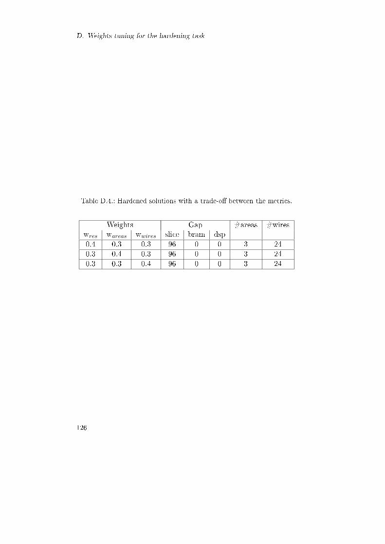
D. Weights tuning for the hardening task
Table D.4.: Hardened solutions with a trade-o� between the metrics.
Weights Gap #areas #wireswres wareas wwires slice bram dsp0.4 0.3 0.3 96 0 0 3 240.3 0.4 0.3 96 0 0 3 240.3 0.3 0.4 96 0 0 3 24
126
Bibliography
[1] C. Bolchini, A. Miele, and C. Sandionigi. A novel design method-ology for implementing reliability-aware systems on SRAM-basedFPGAs. Transactions on Computers, 2010.
[2] T. Kuwahara. FPGA-based Recon�gurable On-board ComputingSystems for Space Applications. PhD thesis, Universitat Stuttgart,Institute of Space Systems, 2009.
[3] R. Katz, K. LaBel, J. J. Wang, B. Cronquist, R. Koga, S. Penzin,and G. Swift. Radiation e�ectcs on current �eld programmabletechnologies. IEEE Trans. Nuclear Science, 6(44):1945�1956, 1997.
[4] C. Carmichael, M. Ca�rey, and A. Salazar. Correcting Single-EventUpsets Through Virtex Partial Con�guration. Technical ReportXAPP216, Xilinx Inc., June 2000.
[5] ITRS. International Technology Roadmap for Semiconductors.http://www.itrs.net/links/2010itrs/home2010.htm.
[6] S. D'Angelo, C. Metra, S. Pastore, A. Pogutz, and G. R. Sechi.Fault-Tolerant Voting Mechanism and Recovery Scheme for TMRFPGA-Based Systems. In Proc. IEEE Int. Symp. Defect and Fault-Tolerance in VLSI Systems, pages 233�240, 1998.
[7] F. Lima Kastensmidt, G. Neuberger, R. F. Hentschke, L. Carro,and R. Reis. Designing Fault-Tolerant Techniques for SRAM-BasedFPGAs. IEEE Design and Test of Computers, 21(6):552�562, 2004.
[8] G. L. Smith and L. de la Torre. Techniques to enable FPGAbased recon�gurable fault tolerant space computing. In Proc. IEEEAerospace Conference, page 11 pp., 2006.
[9] V. Rana, M. Santambrogio, D. Sciuto, B. Kettelhoit, M. Köster,M. Porrmann, and U. Rückert. Partial Dynamic Recon�gurationin a Multi-FPGA Clustered Architecture Based on Linux. In Proc.IEEE Int. Parallel and Distributed Processing Symp., pages 1�8,2007.
127

Bibliography
[10] P. K. Samudrala, J. Ramos, and S. Katkoori. Selective triple Mod-ular redundancy (STMR) based single-event upset (SEU) tolerantsynthesis for FPGAs. IEEE Trans. Nuclear Science, 51(5):2957�2969, October 2004.
[11] C. Bolchini and A. Miele. Design Space Exploration for the Design ofReliable SRAM-based FPGA Systems. In Proc. IEEE Int. Symp. onDefect and Fault-Tolerance in VLSI Systems, pages 332�340, 2008.
[12] K. S. Morgan. SEU-induced Persistent Error Propagation in FP-GAs. PhD thesis, Brigham Young University, 2006.
[13] J. L. Barth, C. S. Dyer, and E. G. Stassinopoulos. Space, Atmo-spheric, and Terrestrial Radiation Environments. IEEE Trans. Nu-clear Science, 50(3), 2003.
[14] ECSS. Methods for the calculation of radiation received and itse�ects, and a policy for design margins. Technical Report ECSS-E-ST-10-12C, European Cooperation for Space Standardization,November 2008.
[15] C. Carmichael and C. W. Tseng. Correcting Single-Event Up-sets in Virtex-4 FPGA Con�guration Memory. Technical ReportXAPP1088, Xilinx, October 2009.
[16] C. Poivey, M. Berg, S. Stansberry, M. Friendlich, H. Kim, D. Pet-rick, and K. LaBel. Heavy ion SEE test of Virtex4 FPGAXC4VFX60 from Xilinx. Technical Report T021607XC4VFX60,Muniz Engineering Inc., University of Southern California, NASA-GSFC, June 2007.
[17] D. Petrick, W. Powell, J. W. Howard Jr., and K. A. LaBel. Virtex-IIPro SEE Test Methods and Results. In Military and Aerospace Ap-plications of Programmable Devices and Technologies Conf., 2004.
[18] S. Srinivasan, P. Mangalagiri, Y. Xie, N. Vijaykrishnan, andK. Sarpatwari. FLAW: FPGA Lifetime AWareness. In Proc. DesignAutomation Conf., 2006.
[19] S. Srinivasan, R. Krishnan, P. Mangalagiri, Y. Xie, V. Narayanan,M. J. Irwin, and K. Sarpatwari. Toward Increasing FPGA Lifetime.IEEE Trans. Dependable and Secure Computing, 5(2):115 � 127,2008.
128
Bibliography
[20] S. Hauck, G. Borriello, and C. Ebeling. Mesh routing topologiesfor multi-fpga systems. In IEEE Proc. Int. Conf. Computer Design:VLSI in Computer & Processors, pages 170�177, 1994.
[21] Xilinx. Spartan-3 FPGA Family Data Sheet. Technical ReportDS099, December 2009.
[22] Xilinx. Virtex-II Platform FPGA: Complete Data Sheet. TechnicalReport DS031, March 2005.
[23] Xilinx. Virtex-4 FPGA Con�guration User Guide. Technical ReportUG071, August 2010.
[24] Xilinx. Virtex-5 FPGA Con�guration User Guide. Technical ReportUG191, June 2009.
[25] Synplicity. HAPS-34. http://www.synopsys.com/home.aspx.
[26] David P. Montminy, Rusty O. Baldwin, Paul D. Williams, andBarry E. Mullins. Using relocatable bitstreams for fault tolerance.In Proc. of NASA/ESA Conf. on Adaptive Hardware and Systems,pages 701�708, 2007.
[27] X. Iturbe, K. Benkrid, T. Arslan, I. Martinez, M. Azkarate, andM.D. Santambrogio. A Roadmap for Autonomous Fault-TolerantSystems. In Proc. Conf. Design and Architectures for Signal andImage Processing, pages 311�321, 2010.
[28] S. Mitra, W.-J. Huang, N.R. Saxena, S.-Y. Yu, and E.J. McCluskey.Recon�gurable Architecture for Autonomous Self-Repair. IEEE De-sign & Test of Comp., 21:228�240, May 2004.
[29] R. Noji, S. Fujie, Y. Yoshikawa, H. Ichihara, and T. Inoue. AnFPGA-based fail-soft system with adaptive recon�guration. In Proc.Intl. On-Line Testing Symp., pages 127�132, 2010.
[30] Xilinx Inc. http://www.xilinx.com.
[31] Frank Vahid. I/O and performance tradeo�s with the FunctionBusduring multi-FPGA partitioning. In Proceedings of the 1997 ACMFifth International Symposium on Field-Programmable Gate Arrays,pages 27�34, 1997.
[32] Iyad Ouaiss, Sriram Govindarajan, Vinoo Srinivasan, MeenakshiKaul, and Ranga Vemuri. An integrated partitioning and synthesissystem for dynamically recon�gurable multi-fpga architectures. In
129
Bibliography
In Proceedings of Parallel and Distributed Processing, pages 31�36,1998.
[33] Preetham Lakshmikanthan, Sriram Govindarajan, Vinoo Srini-vasan, and Ranga Vemuri. Behavioral partitioning with synthesisfor multi-fpga architectures under interconnect, area, and latencyconstraints. In Proceedings of the 15 IPDPS 2000 Workshops onParallel and Distributed Processing, pages 924�931, 2000.
[34] Kalapi Roy and Carl Sechen. A timing driven n-way chip and multi-chip partitioner. In Proceedings of the 1993 IEEE/ACM interna-tional conference on Computer-aided design, pages 240�247, 1993.
[35] S. Hauck and G. Borriello. Logic partition orderings for multi-fpgasystems. In Field-Programmable Gate Arrays, 1995. FPGA '95.Proceedings of the Third International ACM Symposium on, pages32 � 38, 1995.
[36] Kalapi Roy-Neogi and Carl Sechen. Multiple FPGA partitioningwith performance optimization. In Proceedings of the 1995 ACMThird International Symposium on Field-Programmable Gate Ar-rays, pages 146�152, 1995.
[37] J.I. Hidalgo, J. Lanchares, and R. Hermida. Partitioning and place-ment for multi-FPGA systems using genetic algorithms. In Euromi-cro Conference, 2000. Proceedings of the 26th, volume 1, pages 204�211 vol.1, 2000.
[38] J.I. Hidalgo, R. Baraglia, R. Perego, J. Lanchares, and F. Tirado.A parallel compact genetic algorithm for multi-fpga partitioning. InParallel and Distributed Processing, 2001. Proceedings. Ninth Eu-romicro Workshop on, pages 113 �120, 2001.
[39] Nam Sung Woo and Jaeseok Kim. An e�cient method of partition-ing circuits for multiple-FPGA implementation. In Proceedings ofthe 30th international Design Automation Conference, pages 202�207, 1993.
[40] Roman Kuºnar, Franc Brglez, and Krzysztof Kozminski. Cost min-imization of partitions into multiple devices. In Proceedings of the30th international Design Automation Conference, pages 315�320,1993.
[41] Nan-Chi Chou, Lung-Tien Liu, Chung-Kuan Cheng, Wei-Jin Dai,and Rodney Lindelof. Circuit partitioning for huge logic emula-
130
Bibliography
tion systems. In Proceedings of the 31st annual Design AutomationConference, pages 244�249, 1994.
[42] Roman Kuºnar, Franc Brglez, and Baldomir Zajc. Multi-way netlistpartitioning into heterogeneous FPGAs and minimization of totaldevice cost and interconnect. In Proceedings of the 31st annualDesign Automation Conference, pages 238�243, 1994.
[43] Dennis J.-H. Huang and Andrew B. Kahng. Multi-way system par-titioning into a single type or multiple types of FPGAs. In Proceed-ings of the 1995 ACM Third International Symposium on Field-Programmable Gate Arrays, pages 140�145, 1995.
[44] Prashant Sawkar and Donald Thomas. Multi-way partitioning forminimum delay for look-up table based FPGAs. In Proceedings ofthe 32nd annual ACM/IEEE Design Automation Conference, pages201�210, 1995.
[45] Wen-Jong Fang and Allen C.-H. Wu. Performance-driven multi-FPGA partitioning using functional clustering and replication. InProceedings of the 35th annual Design Automation Conference,pages 283�286, 1998.
[46] Helena Krupnova and Gabriele Saucier. Iterative improvementbased multi-way netlist partitioning for FPGAs. In Proceedings ofthe Conference on Design, Automation and Test in Europe, 1999.
[47] C. Bolchini, A. Miele, and C. Sandionigi. Automated resource-aware�oorplanning of recon�gurable areas in partially-recon�gurableFPGA systems. In Int. Conf. on Field Programmable Logic andApplications, 2011, To appear.
[48] L. Wolsey. Integer Programming. John Wiley and Sons, 1998.
[49] Sadiq M. Sait and Habib Youssef. VLSI physical design automation.World Scienti�c Publishing Co. Pte. Ltd., 2004.
[50] C. Bolchini, L. Fossati, D. Merodio Codinachs, A. Miele, and C. San-dionigi. A Reliable Recon�guration Controller for Fault-TolerantEmbedded Systems on Multi-FPGA Platforms. In Proc. IEEE Int.Symp. Defect and Fault Tolerance in VLSI Systems, 2010.
[51] C. Bolchini and C. Sandionigi. Fault Classi�cation for SRAM-basedFPGAs in the Space Environment for Fault Mitigation. IEEE Em-bedded Systems Letters, 2010.
131
Bibliography
[52] Salvatore Pontarelli, Marco Ottavi, Vamsi Vankamamidi,Gian Carlo Cardarilli, Fabrizio Lombardi, and Adelio Sal-sano. Analysis and evaluations of reliability of recon�gurable fpgas.Journal of Electronic Testing, 24(1-3):105�116, 2008.
[53] F. A. Bower, D. J. Sorin, and S. Ozev. A Mechanism for OnlineDiagnosis of Hard Faults in Microprocessors. In Int. Symp. on Mi-croarchitecture, pages 197 � 208, 2005.
[54] European Space Agency. SPENVIS. http://www.spenvis.oma.be/.
[55] R. H. Maurer, M. E. Fraeman, M. N. Martin, and D. R. Roth.Harsh Environments: Space Radiation Environment, E�ects andMitigation. Johns Hopkins APL Technical Digest, 28(1), 2008.
[56] V. Bocci, M. Carletti, G. Chiodi, E. Gennari, E. Petrolo, A. Sala-mon, R. Vari, and S. Veneziano. Radiation test and application ofFPGAs in the ATLAS Level 1 Trigger. In Workshop on Electronicsfor LHC Experiments, 2001.
[57] P. Alfke. Xilinx FPGAs: A Technical Overview for the First-TimeUser. Technical Report XAPP097, Xilinx, December 1998.
[58] C. Claus, B. Zhang, W. Stechele, L. Braun, M. Hübner, andJ. Becker. A multi-platform controller allowing for maximum Dy-namic Partial Recon�guration throughput. In Proc. Int. Conf. FieldProgrammable Logic and Applications, pages 535�538, 2008.
[59] C. Claus, F. H. Muller, J. Zeppenfeld, and W. Stechele. Anew framework to accelerate Virtex-II Pro dynamic partial self-recon�guration. In Proc. IEEE Int. Parallel and Distributed Pro-cessing Symp., pages 1�7, 2007.
[60] A. Cuoccio, P. R. Grassi, V. Rana, M. D. Santambrogio, and D. Sci-uto. A Generation Flow for Self-Recon�guration Controllers Cus-tomization. In IEEE Int. Workshop Electronic Design, Test andApplications, pages 279�284, 2008.
[61] S. Bayar and A. Yurdakul. Dynamic Partial Self-Recon�gurationon Spartan-III FPGAs via a Parallel Con�guration Access Port(PCAP). In Proc. HiPEAC Workshop on Recon�gurable Computing,2008.
[62] Xilinx. Virtex-II Pro and Virtex-II Pro X FPGA User Guide. Tech-nical Report UG012, November 2007.
132
Bibliography
[63] Xilinx. OPB HWICAP Product Speci�cation. Technical ReportDS280, March 2004.
[64] M. Sonza Reorda, M. Violante, C. Meinhardt, and R. Reis. A low-cost SEE mitigation solution for soft-processors embedded in sys-tems on programmable chips. In Proceedings of the Conference onDesign, Automation and Test in Europe, pages 352�357, 2009.
[65] ESA Microelectronics. LEON2-FT. Website, 2009. http://www.
esa.int/TEC/Microelectronics/SEMUD70CYTE_0.html.
[66] D. Nikolos. Self-testing embedded two-rail checkers. J. ElectronicTesting, Theory and Applications, 12(1-2):69�79, 1998.
[67] Xilinx Inc. Reading User Data from Con�guration PROMs. Tech-nical Report XAPP694, Xilinx Inc., November 2007.
[68] Xilinx Inc. Xilinx TMRTool, 2006.
[69] Conrado Pilotto, José Rodrigo Azambuja, and Fernanda Lima Kas-tensmidt. Synchronizing triple modular redundant designs in dy-namic partial recon�guration applications. In Proceedings of the21st annual symposium on Integrated circuits and system design,pages 199�204. ACM, 2008.
133