Embed Size (px)
Citation preview
A Resonant Clock Generator for Single-Phase Adiabatic Systems
Conrad H. Ziesler
Marios C. Papaefthymiou
University of Michigan, Ann Arbor, MI
Suhwan Kim IBM, T.J. Watson Research Center, Yorktown Heights, NY
Advanced Computer Architecture LaboratoryDepartment of Electrical Engineering and Computer Science University of Michigan, Ann Arbor, MI
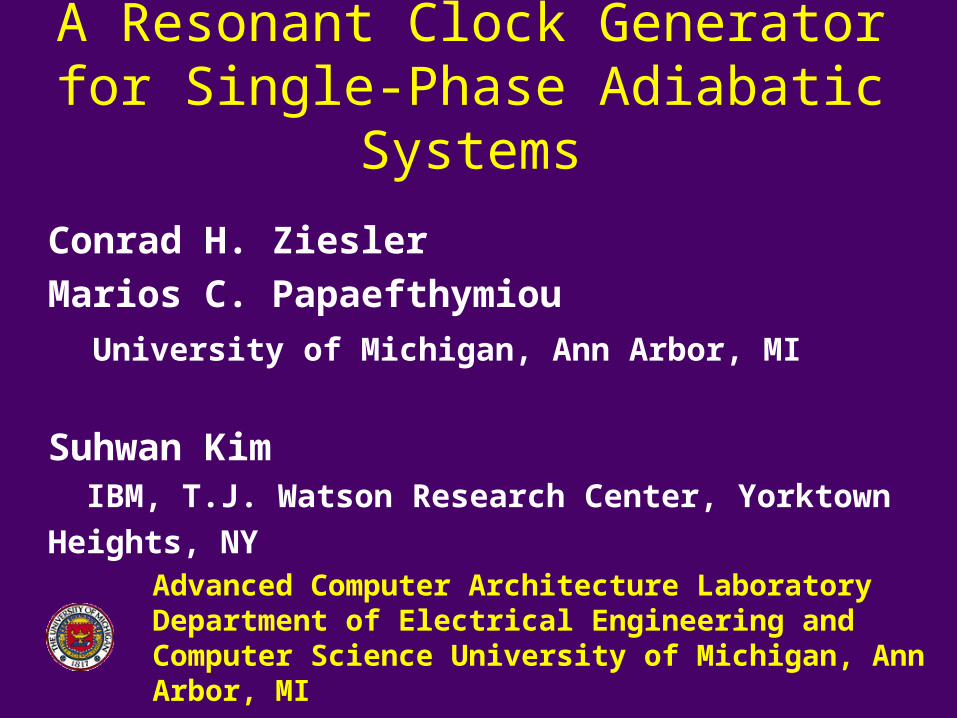
Motivation• Practical single-phase charge-recovery chip @ 200MHz
• Efficient and simple integrated clock generator
Clock Generator
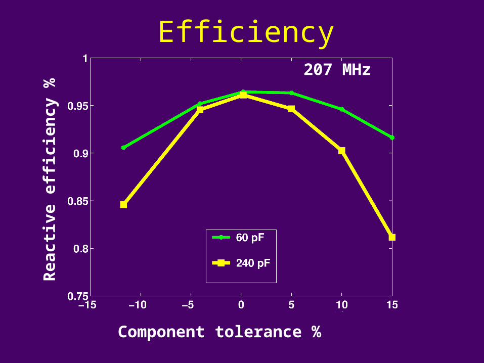
Efficiency
Component tolerance %
207 MHzReactive efficiency %
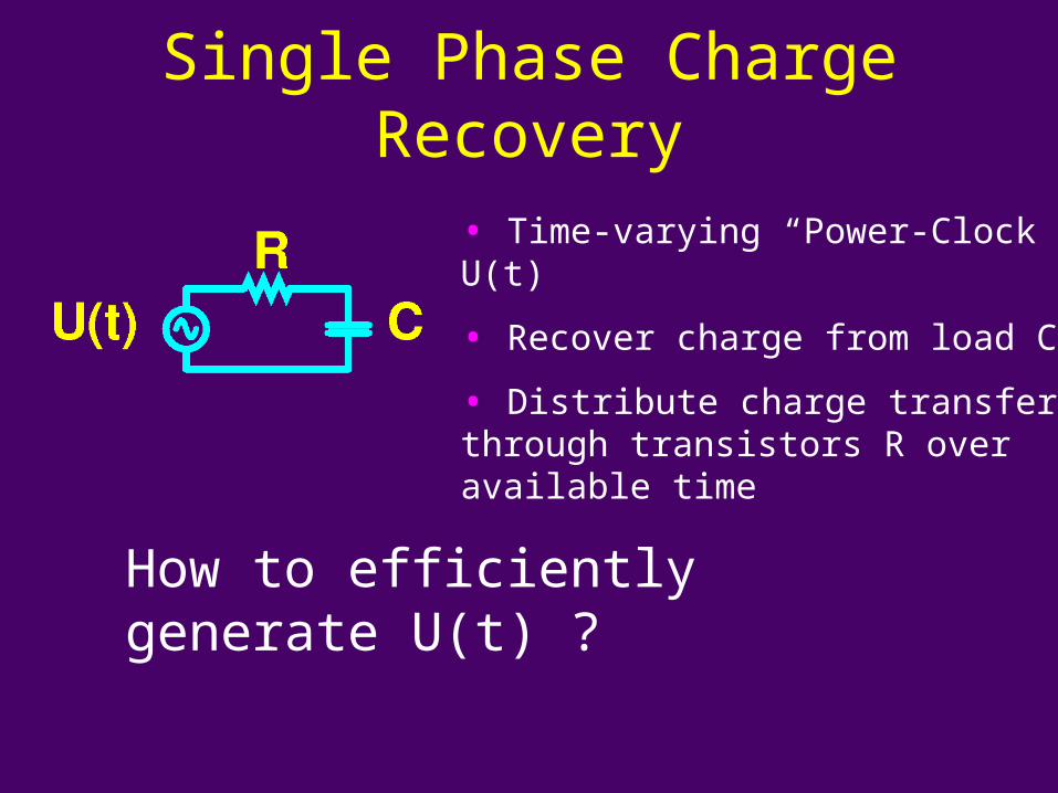
Single Phase Charge Recovery
• Time-varying “Power-Clock” U(t)
• Recover charge from load C
• Distribute charge transfer through transistors R over available time
How to efficiently generate U(t) ?
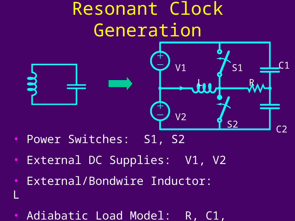
Resonant Clock Generation
R
C1
C2
L
S1
S2
V1
V2
• Power Switches: S1, S2
• External DC Supplies: V1, V2
• External/Bondwire Inductor: L
• Adiabatic Load Model: R, C1, C2
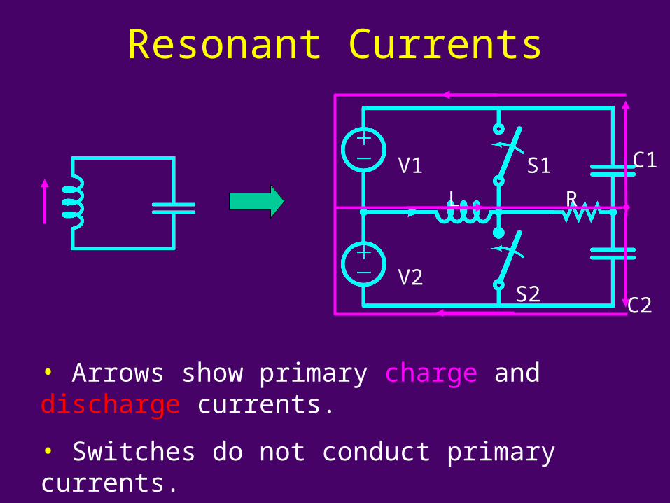
Resonant Currents
R
C1
C2
L
S1
S2
V1
V2
• Arrows show primary charge and discharge currents.
• Switches do not conduct primary currents.
• Switches can therefore be relatively small and efficient.
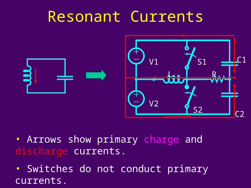
Resonant Currents
R
C1
C2
L
S1
S2
V1
V2
• Arrows show primary charge and discharge currents.
• Switches do not conduct primary currents.
• Switches can therefore be relatively small and efficient.
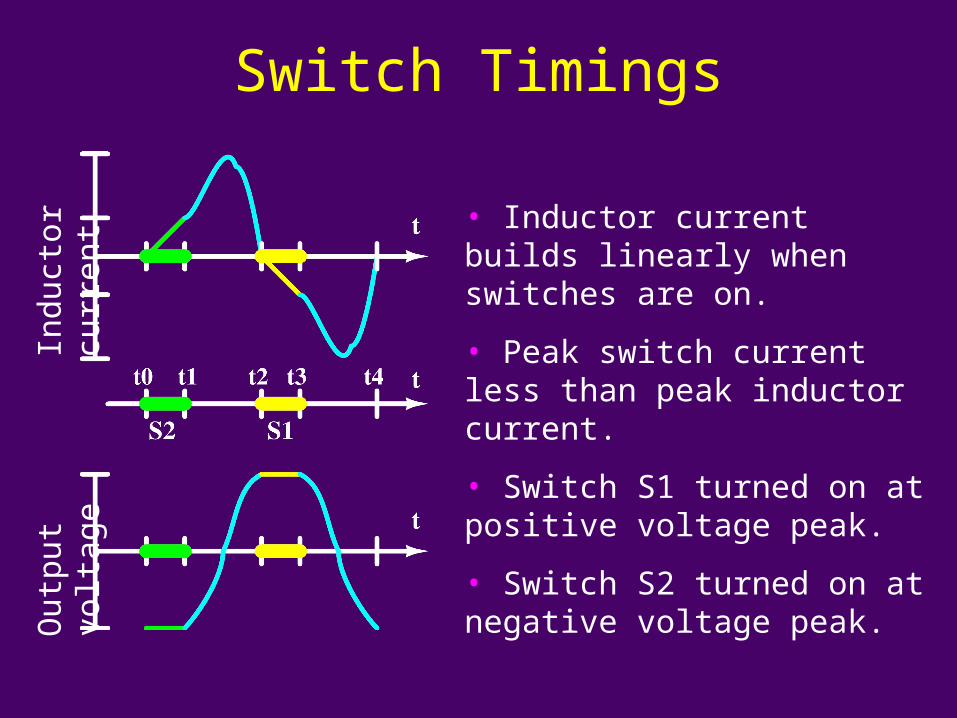
Switch Timings
• Inductor current builds linearly when switches are on.
• Peak switch current less than peak inductor current.
• Switch S1 turned on at positive voltage peak.
• Switch S2 turned on at negative voltage peak.
Indu
ctor
cur
rent
Out
put v
olta
ge
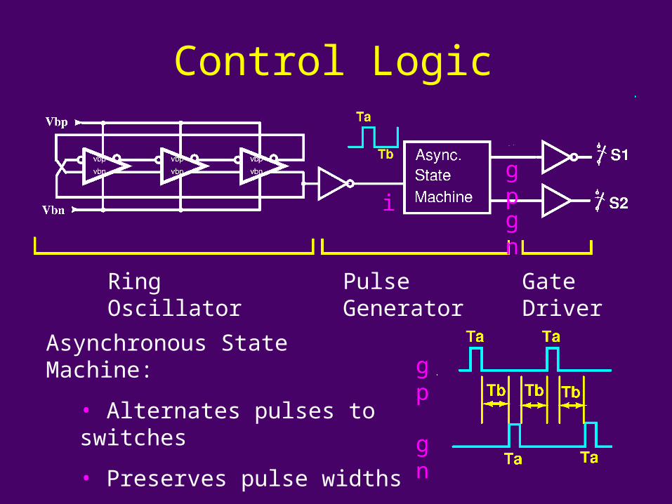
Control Logic
Ring Oscillator Pulse Generator Gate Driver
i
gp
gn
gp
gn
Asynchronous State Machine:
• Alternates pulses to switches
• Preserves pulse widths
• Halves frequency
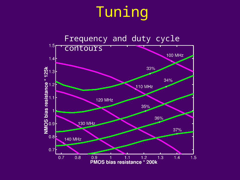
Tuning
Frequency and duty cycle contours
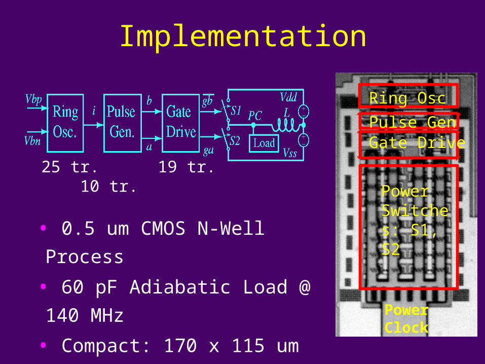
Implementation
• 0.5 um CMOS N-Well Process
• 60 pF Adiabatic Load @ 140 MHz
• Compact: 170 x 115 um
• External ~10 nH InductorPower Clock
Pulse Gen
Ring Osc
Gate Drive
Power Switches: S1, S2
25 tr. 19 tr. 10 tr.
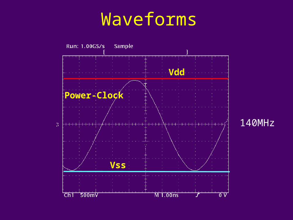
Waveforms
Vdd
Vss
Power-Clock
140MHz
Conclusion
• Resonant LC based clock generator
• Reactive efficiencies over 90% @ 200 MHz
• Compact design, 0.019 mm^2
• Scalable to large capacitive loads
• Fabricated in a 0.5 um standard CMOS process
• Tested with real adiabatic circuit, ~60 pF @ 140 MHz
Acknowledgments
This research was supported in part by the US Army Research Office under ASSERT Grant No. DAAG55-97-1-0250 and Grant No. DAAD19-99-1-0304
Fabrication performed by: MOSIS Integrated Circuit Prototyping Service
Advanced Computer Architecture LaboratoryDepartment of Electrical Engineering and Computer Science University of Michigan, Ann Arbor, MI
For Additional Information
www.eecs.umich.edu/acal/adiabaticConrad Ziesler, [email protected] Kim, [email protected] Papaefthymiou, [email protected]
A Single-Phase Resonant Clock Generator ISLPED, Aug. 2001Design, Test, and Measurement of a True Single-Phase Adiabatic Multiplier ARVLSI, March 2001A True Single-Phase 8-bit Adiabatic Multiplier DAC, June 2001True Single-Phase Adiabatic Circuitry IEEE Trans. VLSI, Feb. 2001