Embed Size (px)
Citation preview
Received September 23, 2020, accepted October 3, 2020, date of publication October 6, 2020, date of current version October 19, 2020.
Digital Object Identifier 10.1109/ACCESS.2020.3029127
A Review and Analysis of Automatic OpticalInspection and Quality Monitoring Methodsin Electronics IndustryABD AL RAHMAN M. ABU EBAYYEH AND ALIREZA MOUSAVI, (Senior Member, IEEE)Department of Electronic and Computer Engineering, Brunel University London, Uxbridge UB8 3PH, U.K.
Corresponding author: Abd Al Rahman M. Abu Ebayyeh ([email protected])
This work has been carried out in the framework of the IQONIC Project, which received funding from the European Union’s Horizon 2020Research and Innovation Program under Grant agreement No. 820677.
ABSTRACT Electronics industry is one of the fastest evolving, innovative, and most competitive industries.In order to meet the high consumption demands on electronics components, quality standards of the productsmust be well-maintained. Automatic optical inspection (AOI) is one of the non-destructive techniques used inquality inspection of various products. This technique is considered robust and can replace human inspectorswho are subjected to dull and fatigue in performing inspection tasks. A fully automated optical inspectionsystem consists of hardware and software setups. Hardware setup include image sensor and illuminationsettings and is responsible to acquire the digital image, while the software part implements an inspectionalgorithm to extract the features of the acquired images and classify them into defected and non-defectedbased on the user requirements. A sorting mechanism can be used to separate the defective products fromthe good ones. This article provides a comprehensive review of the various AOI systems used in electronics,micro-electronics, and opto-electronics industries. In this review the defects of the commonly inspectedelectronic components, such as semiconductor wafers, flat panel displays, printed circuit boards and lightemitting diodes, are first explained. Hardware setups used in acquiring images are then discussed in termsof the camera and lighting source selection and configuration. The inspection algorithms used for detectingthe defects in the electronic components are discussed in terms of the preprocessing, feature extraction andclassification tools used for this purpose. Recent articles that used deep learning algorithms are also reviewed.The article concludes by highlighting the current trends and possible future research directions.
INDEX TERMS Automatic optical inspection, classification algorithms, electronics industry, featureextraction, image processing, image sensor, machine learning, machine vision.
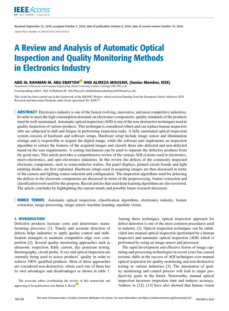
I. INTRODUCTIONDefective products increase costs and deteriorates manu-facturing processes [1]. Timely and accurate detection ofdefects helps industries to apply quality control and stabi-lization strategies to maintain competitive edge over com-petition [2]. Several quality monitoring approaches such asultrasonic inspection, Eddy current, dye penetrant testing,thermography, circuit probe, X-ray and optical inspection arecurrently being used to assess products’ quality in order toachieve 100% qualified products. Most of these approachesare considered non-destructive, where each one of them hasits own advantages and disadvantages as shown in table 1.
The associate editor coordinating the review of this manuscript and
approving it for publication was Mehul S. Raval .
Among these techniques, optical inspection approach fordefect detection is one of the most common procedures usedin industry [3]. Optical inspection techniques can be subdi-vided into manual optical inspection (performed by a humaninspector) and automatic optical inspection (AOI) which isperformed by using an image sensor and processor.
The rapid development and effective fusion of image cap-turing and processing technologies in recent years has causedtectonic shifts in the success of AOI techniques over manualoptical inspection for quality monitoring and non-destructivetesting in various industries [3]. The automation of qual-ity monitoring and control process will lead to major pro-ductivity gains in the future. Noteworthy, manual opticalinspection increases inspection time and reduces accuracy.Authors in [12], [13] have also showed that human vision
183192 This work is licensed under a Creative Commons Attribution 4.0 License. For more information, see https://creativecommons.org/licenses/by/4.0/ VOLUME 8, 2020
A. M. Abu Ebayyeh, A. Mousavi: Review and Analysis of Automatic Optical Inspection and Quality Monitoring Methods
TABLE 1. Summary of quality monitoring approaches used in industrial inspection.
VOLUME 8, 2020 183193
A. M. Abu Ebayyeh, A. Mousavi: Review and Analysis of Automatic Optical Inspection and Quality Monitoring Methods
inspection capabilities declines with dull and endlessly rou-tine jobs (i.e. fatigue). On the other hand, modern captur-ing devices are capable of detecting tiny defective featuresand features with low intensity and contrast that even themost experienced inspectors cannot detect them using theirnaked eye. Recent studies have also revealed that humanscannot handle identifying color defects as color is psycho-logical perception even though it is triggered by physicalradiation [14], [15]. Automated machine vision data cap-ture system have paved a way for large scale observationshelping to gather statistically viable information for qualityanalysis and assurance methods [16], [17]. Chen and Harlowin [13] gave six productivity and efficiency reasons for usingAOI instead of manual inspection. Freeing humans fromthe dull and routine, saving human labour costs, performinginspection in unfavorable environment, reducing demand forhighly skilled human inspectors, analyzing statistics on testinformation and keeping records for management and deci-sions, and matching high speed production with high speedinspection. To add to these, one can include the expansion inscale, scope, application, and techniques that provide depth,breadth and multiple perspectives.
Recently, AOI algorithms were further enhanced by inte-grating them with machine learning techniques and deeplearning, which at occasions could improve the resultand speed of the detection process remarkably [18], [19].Timm and Barth in [20] suggested that an AOI algorithmmust satisfy two major requirements; 100% detection rateand minimum false alarm rate. Convolutional Neural Net-works (CNN) was one of the common used deep learningalgorithms recently for inspection purposes [21]. The reasonbehind this is because CNNs are specialized in dealing withimage data. Furthermore, it does not need feature extractionor preprocessing for the images. Hence, preprocessing andfeature extraction processes are embedded within the hiddenlayers of the CNN.
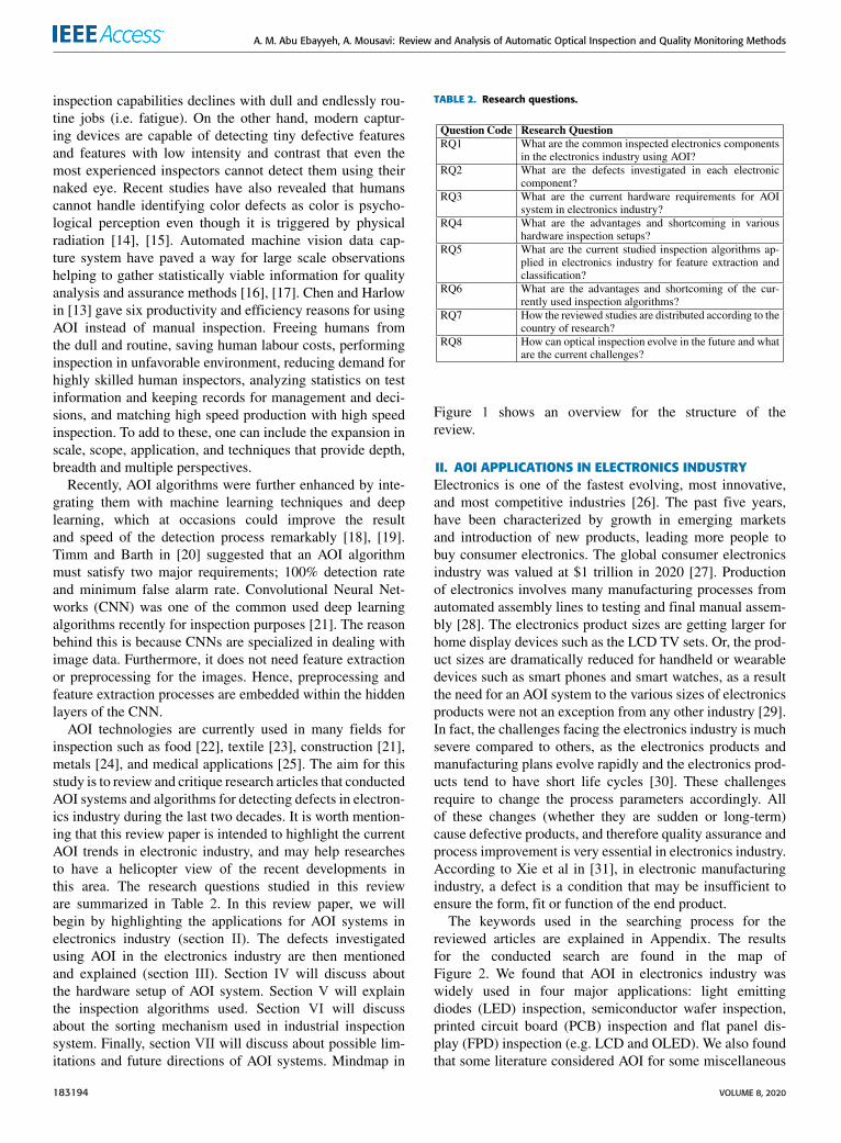
AOI technologies are currently used in many fields forinspection such as food [22], textile [23], construction [21],metals [24], and medical applications [25]. The aim for thisstudy is to review and critique research articles that conductedAOI systems and algorithms for detecting defects in electron-ics industry during the last two decades. It is worth mention-ing that this review paper is intended to highlight the currentAOI trends in electronic industry, and may help researchesto have a helicopter view of the recent developments inthis area. The research questions studied in this revieware summarized in Table 2. In this review paper, we willbegin by highlighting the applications for AOI systems inelectronics industry (section II). The defects investigatedusing AOI in the electronics industry are then mentionedand explained (section III). Section IV will discuss aboutthe hardware setup of AOI system. Section V will explainthe inspection algorithms used. Section VI will discussabout the sorting mechanism used in industrial inspectionsystem. Finally, section VII will discuss about possible lim-itations and future directions of AOI systems. Mindmap in
TABLE 2. Research questions.
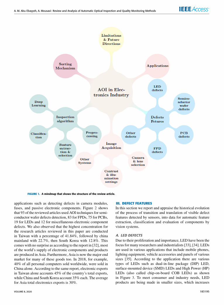
Figure 1 shows an overview for the structure of thereview.
II. AOI APPLICATIONS IN ELECTRONICS INDUSTRYElectronics is one of the fastest evolving, most innovative,and most competitive industries [26]. The past five years,have been characterized by growth in emerging marketsand introduction of new products, leading more people tobuy consumer electronics. The global consumer electronicsindustry was valued at $1 trillion in 2020 [27]. Productionof electronics involves many manufacturing processes fromautomated assembly lines to testing and final manual assem-bly [28]. The electronics product sizes are getting larger forhome display devices such as the LCD TV sets. Or, the prod-uct sizes are dramatically reduced for handheld or wearabledevices such as smart phones and smart watches, as a resultthe need for an AOI system to the various sizes of electronicsproducts were not an exception from any other industry [29].In fact, the challenges facing the electronics industry is muchsevere compared to others, as the electronics products andmanufacturing plans evolve rapidly and the electronics prod-ucts tend to have short life cycles [30]. These challengesrequire to change the process parameters accordingly. Allof these changes (whether they are sudden or long-term)cause defective products, and therefore quality assurance andprocess improvement is very essential in electronics industry.According to Xie et al in [31], in electronic manufacturingindustry, a defect is a condition that may be insufficient toensure the form, fit or function of the end product.
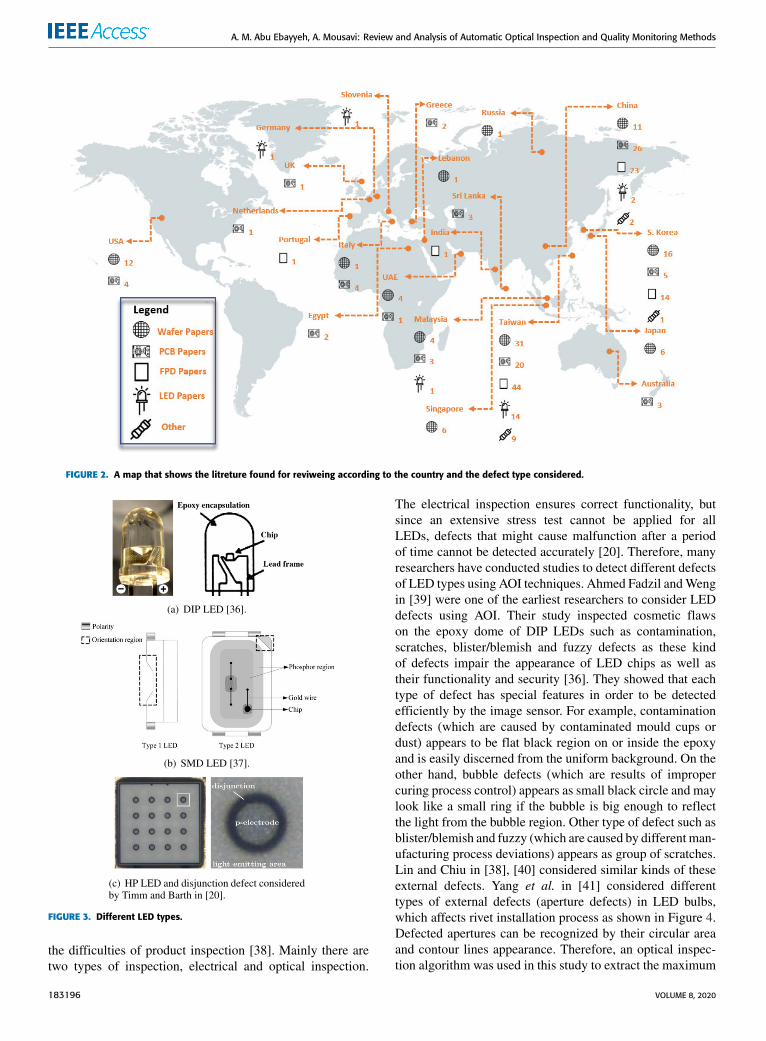
The keywords used in the searching process for thereviewed articles are explained in Appendix. The resultsfor the conducted search are found in the map ofFigure 2. We found that AOI in electronics industry waswidely used in four major applications: light emittingdiodes (LED) inspection, semiconductor wafer inspection,printed circuit board (PCB) inspection and flat panel dis-play (FPD) inspection (e.g. LCD and OLED). We also foundthat some literature considered AOI for some miscellaneous
183194 VOLUME 8, 2020
A. M. Abu Ebayyeh, A. Mousavi: Review and Analysis of Automatic Optical Inspection and Quality Monitoring Methods
FIGURE 1. A mindmap that shows the structure of the review article.
applications such as detecting defects in camera modules,fuses, and passive electronic components. Figure 2 showsthat 93 of the reviewed articles used AOI techniques for semi-conductor wafer defects detection, 83 for FPDs, 75 for PCBs,19 for LEDs and 12 for miscellaneous electronic componentdefects. We also observed that the highest concentration forthe research articles reviewed in this paper are conductedin Taiwan with a percentage of 41.84%, followed by chinamainland with 22.7%, then South Korea with 12.8%. Thiscomeswith no surprise as according to the report in [32], mostof the world’s supply of electronic components and productsare produced in Asia. Furthermore, Asia is now the major endmarket for many of these goods too. In 2018, for example,40% of all personal computers sold worldwide, were sold inChina alone. According to the same report, electronic exportsin Taiwan alone accounts 45% of the country’s total exports,while China and South Korea account 35% each. The averagefor Asia total electronics exports is 30%.
III. DEFECT FEATURESIn this section we report and appraise the historical evolutionof the process of transition and translation of visible defectfeatures detected by sensors, into data for automatic featureextraction, classification and evaluation of components byvision systems.
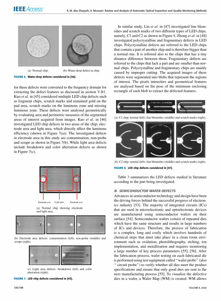
A. LED DEFECTSDue to their proliferation and importance, LED have been thefocus for many researchers and industrialists [33], [34]. LEDsare used in various applications that include mobile phones,lighting equipment, vehicle accessories and panels of varioussizes [35]. According to the application there are varioustypes of LEDs such as dual-in-line package (DIP) LED,surface-mounted device (SMD) LEDs and High Power (HP)LEDs (also called chip-on-board COB LEDs) as shownin Figure 3. To meet consumer and industry needs, LEDproducts are being made in smaller sizes, which increases
VOLUME 8, 2020 183195
A. M. Abu Ebayyeh, A. Mousavi: Review and Analysis of Automatic Optical Inspection and Quality Monitoring Methods
FIGURE 2. A map that shows the litreture found for reviweing according to the country and the defect type considered.
FIGURE 3. Different LED types.
the difficulties of product inspection [38]. Mainly there aretwo types of inspection, electrical and optical inspection.
The electrical inspection ensures correct functionality, butsince an extensive stress test cannot be applied for allLEDs, defects that might cause malfunction after a periodof time cannot be detected accurately [20]. Therefore, manyresearchers have conducted studies to detect different defectsof LED types using AOI techniques. Ahmed Fadzil andWengin [39] were one of the earliest researchers to consider LEDdefects using AOI. Their study inspected cosmetic flawson the epoxy dome of DIP LEDs such as contamination,scratches, blister/blemish and fuzzy defects as these kindof defects impair the appearance of LED chips as well astheir functionality and security [36]. They showed that eachtype of defect has special features in order to be detectedefficiently by the image sensor. For example, contaminationdefects (which are caused by contaminated mould cups ordust) appears to be flat black region on or inside the epoxyand is easily discerned from the uniform background. On theother hand, bubble defects (which are results of impropercuring process control) appears as small black circle and maylook like a small ring if the bubble is big enough to reflectthe light from the bubble region. Other type of defect such asblister/blemish and fuzzy (which are caused by different man-ufacturing process deviations) appears as group of scratches.Lin and Chiu in [38], [40] considered similar kinds of theseexternal defects. Yang et al. in [41] considered differenttypes of external defects (aperture defects) in LED bulbs,which affects rivet installation process as shown in Figure 4.Defected apertures can be recognized by their circular areaand contour lines appearance. Therefore, an optical inspec-tion algorithm was used in this study to extract the maximum
183196 VOLUME 8, 2020

A. M. Abu Ebayyeh, A. Mousavi: Review and Analysis of Automatic Optical Inspection and Quality Monitoring Methods
FIGURE 4. LED cup aperture defects studied in [41].
inscribed circles of the apertures and calculate the diametersfor evaluation.
Perng et al. in [37] considered investigating Type 1 andType 2 SMD LEDs shown in Figure 3(b). An orientationregion was labelled in both types to distinguish their polar-ities. In Type 2 LED, there are three gold wires and a chip inthe phosphor region. The quality of the phosphor region influ-ences the LED illuminating efficiency. Defects of lightingphosphor region can be inspected visually in Type 2; however,the lighting phosphor region of Type 1 cannot be seen due toits physical placement when it is packaged. Therefore, in thisstudy, only external defects are considered in Type 1 LED.Generally speaking, the defects in both types take placeduring fabrication and taping processes. Examples of thesedefects are mouse bites, missing gold wires, surface flaws,missing component, wrong orientation and inverse polarity.These defects can be identified visually by converting theacquired image of a sample LED into a binary image andexamine the number of pixels of the segmented areas thatrepresent the regions of interest. Perng et al. in [33] consid-ered the same types in their study. However, they subdividedType 1 LED into 2 sub-types, namely, small polarity and bigpolarity for better defect classification A similar approachproposed by Kuo et al. in [42] to detect missing component,no chip, wire shift and foreignmaterial defects in SMDLEDs.
Some researchers considered evaluating the light intensityand other physical properties of LEDs using AOI system.Bürmen et al. in [43] analysed the optical properties of LEDsby projecting the LED light on screen and analyzing theimage of the resulted projection. The optical properties stud-ied in this paper were intensity, mean color, color variation,viewing angle and divergence of the optical axis. In orderfor them to conduct the study, they connected in series twoLEDs; one of them were a reference LED (non-defected) andthe other were the LED for testing purposes, to pass the sameelectrical current for both. The reflected light for both LEDsfrom a screen were captured by image sensors for furtheranalysis. The optical properties of the reference LED were
FIGURE 5. Image acquiring technique considered in [43].
compared to the one for testing. One drawback in this methodthat through the testing process the properties of the referenceLED may change by time, and therefore the testing may notbe reliable.
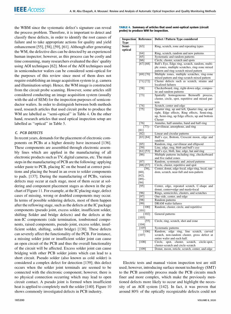
Other researchers considered internal LED defectsthat take place in the LED die regions, where suchdefects are considered hard to detect and need specialarrangement such as scanning electron microscope (SEM).Chang et al. in [44] proposed an AOI system to detectdefective dies in a four-element wafer, such that each waferconsists of more than 8000 dies and the physical area of eachdie is about 200 µm × 200 µm. The die first were dividedinto three regions: light-emitting area, p-electrode, and back-ground. The inspection of the die regions was performedgeometrically and heuristically. In geometric inspection thedie size, width, height, the electrode radius, and the centerof the electrode are evaluated according to pixel intensities.In heuristic inspection, abnormal regions in the image areevaluated such as empty pixels in light-emitting region.Timm and Barth in [20] followed the same path in investigat-ing die defects in HP LEDs. They have focused their attentionto the p-electrode of the die and its surrounding area, wherediscontinuity and erosion defects could occur (as shownin Figure 3(c)). Erosion and discontinuity defects cause thep-electrode gets directly connected to the light emitting areaand thus can lead to critical malfunction of the LED. Sincep-electrodes are circular regions, radially encoded featureswere examined to look for pixels intensities that could indi-cate a presence of a discontinuity defect. Besides the com-plexity of the defects, low contrast and strong image noise ofthese defects make this problem very challenging. Lin in [36]investigated water-drop defects that cause surface blemisheswhich fall across two different background textures in DIPLED chip (shown in Figure 6). This defect occurs due to thesteam generated during the production process. As the casein epoxy packaging defects, these kinds of defects impair theappearance of LEDs as well as their functionality and secu-rity. The detection process of water-drop defect is not straightforward as the blemish has a semi-opaque appearance anda low intensity contrast with the rough exterior of the LEDchip. Moreover, the blemish may fall across two differentbackground textures, which further increases the difficultiesof defect detection. Therefore, the images acquired images
VOLUME 8, 2020 183197
A. M. Abu Ebayyeh, A. Mousavi: Review and Analysis of Automatic Optical Inspection and Quality Monitoring Methods
FIGURE 6. Water-drop defects considered in [36].
for these defects were converted to the frequency domain forextracting the defect features as discussed in section V-B1.Kuo et al. in [45] considered multiple LED chip defects suchas fragment chips, scratch marks and remained gold on thepad area, scratch marks on the luminous zone and missingluminous zone. These defects were analysed geometricallyby evaluating area and perimetric measures of the segmentedareas of interest acquired from images. Kuo et al. in [46]investigated LED chip defects in two areas of the chip; elec-trode area and light area, which directly affect the luminousefficiency (shown in Figure 7(a)). The investigated defectsin electrode area in this study are contamination, non-probeand scrape as shown in Figure 7(b). While light area defectsinclude breakdown and color aberration defects as shownin Figure 7(c).
FIGURE 7. LED chip defects considered in [45].
In similar study, Lin et al. in [47] investigated line blem-ishes and scratch marks of two different types of LED chips,namely, C1 and C2 as shown in Figure 8. Zhong et al. in [48]investigated polycrystalline and fragmentary defects in LEDchips. Polycrystalline defects are referred to the LED chipsthat contain a part of another chip and is therefore bigger thana normal one. It is referred also to the chips that has a tinydistance difference between them. Fragmentary defects arereferred to the chips that lack a part and are smaller than nor-mal chips. Polycrystalline and fragmentary chips are mainlycaused by improper cutting. The acquired images of thesedefects were segmented into blobs that represent the regionsof interest. The pixels intensities and geometrical featuresare analysed based on the pose of the minimum enclosingrectangle of each blob to extract the defected features.
FIGURE 8. LED chip defects considered in [47].
Table 3 summarizes the LED defects studied in literatureaccording to the part being investigated.
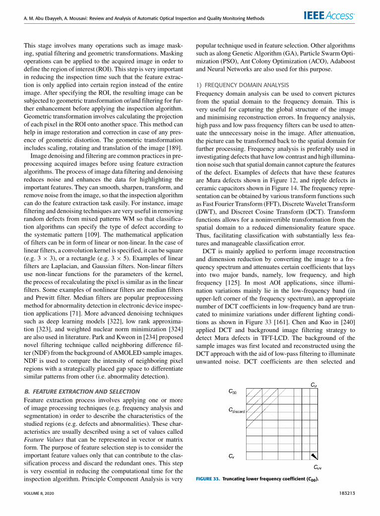
B. SEMICONDUCTOR WAFER DEFECTSAdvances in semiconductor technology and design have beenthe driving forces behind the successful progress of electron-ics industry [53]. The majority of integrated circuits (ICs)that are used in microelectronic and optoelectronic devicesare manufactured using semiconductor wafers on theirsurface [54]. Semiconductor wafers consist of repeated dieswhich have the same structure and results in large numbersof ICs and devices. Therefore, the process of fabricationis a complex, long and costly which involves hundreds ofchemical steps that must take place in a clean room envi-ronment such as oxidation, photolithography, etching, ionimplementation, and metallization and requires monitoringa large number of key process parameters [55], [56]. Afterthe fabrication process, wafer testing on each fabricated dieis performed using test equipment called ‘‘wafer probe’’ (also‘‘ circuit probe’’) to verify whether all dies meet the productspecifications and ensure that only good dies are sent to thenext manufacturing process [55]. To visualize the defectivedies in a wafer, a Wafer Map (WM) is created. WM allows
183198 VOLUME 8, 2020

A. M. Abu Ebayyeh, A. Mousavi: Review and Analysis of Automatic Optical Inspection and Quality Monitoring Methods
TABLE 3. Summary of articles that used AOI system to investigate LEDdefects.
to compare neighbor dies with each other and locate howmany dies are defected visually using a map image [57].Wafer maps are also called Wafer Bin Map (WBM) when thedies are represented in binary form such as the defective dieshas logic ‘1’ and the non-defected has logic ‘0’. Normallythree types of wafer defects occur, which are random defects,systematic defects and mixed defects. Random defects(Figure 9(h)) result from randommanufacturing environmen-tal factors, such as particles in the clean room; these canbecome randomly scattered all over the wafer. Such defectsare long-term and expensive to correct. On the other hand,systematic defects are normally generated by an assignablecause such as a human mistake, particles from equipment,or chemical staining [58]–[60]. Systematic defects usually
follow a specific pattern, for instance, a center pattern (alsoknown as bull’s eye) concentrated in the center of a wafer typ-ically occurs when there are uniformity variations caused bya chemical mechanical process (CMP), the distance betweenthe wafer center and the center of the region is less thanfour dies (shown in Figure 9(a)). A ring pattern (shownin Figure 9(b)) appears along the wafer edge when there isa layer-to-layer misalignment in the storage-node process,which results in a write recovery time failure that is due tothe decreased size of the contact holes, most of the faileddies occur along the wafer edge and encompass more thanfour-fifths of the wafer perimeter. A scratch pattern as shownin Figure 9(d) (also known as line pattern) is caused byagglomerated particles and the hardening of the pad duringthe CMP, where most of the failed dies on the wafer form aline, and the length of the line is five or more dies. A shotpattern (shown in Figure 9(e)) is caused by a probe-cardproblem when multiple dies are simultaneously tested toreduce the test cost. A zone pattern (also known as blob,spot, or cluster) at a specific location on the wafer is causedby non-uniformity or uneven cleaning, where most of thefailed dies on the wafer occur as an arbitrary shape, and thedistance between the wafer center and the center of the regionis more than four dies as shown in Figure 9(g). A checker-board pattern as shown in Figure 9(f) is generated becauseof the mask misalignment during the lithographic process.Mixed defect consists of a random defect and a systematicdefect in one map. Most WMs are of this type. Hence,it is important to separate random and systematic defects in
FIGURE 9. Different WM patterns (red squares indicate defective dies).
VOLUME 8, 2020 183199
A. M. Abu Ebayyeh, A. Mousavi: Review and Analysis of Automatic Optical Inspection and Quality Monitoring Methods
the WBM since the systematic defect’s signature can revealthe process problem. Therefore, it is important to detect andclassify these defects, in order to identify the root causes offailure and to take appropriate actions for quality and yieldenhancement [55], [58], [59], [61]. Although after generatingtheWM, the defective dies can be detected by an experiencedhuman inspector; however, as this process can be costly andtime consuming, many researchers evaluated the dies’ qualityusing AOI techniques [62]. Most of the AOI techniques usedin semiconductor wafers can be considered semi-optical forthe purposes of this review since most of them does notrequire establishing an image acquisition system (e.g. cameraand illumination setup). Hence, theWM image is constructedfrom the circuit probe scanning. However, some articles stillconsidered conducting an image acquisition system (usuallywith the aid of SEM) for the inspection purposes of semicon-ductor wafers. In order to distinguish between both methodsused, research articles that used circuit probe to produce theWM are labelled as ‘‘semi-optical’’ in Table 4. On the otherhand, research articles that used optical inspection setup arelabelled as ‘‘optical’’ in Table 5.
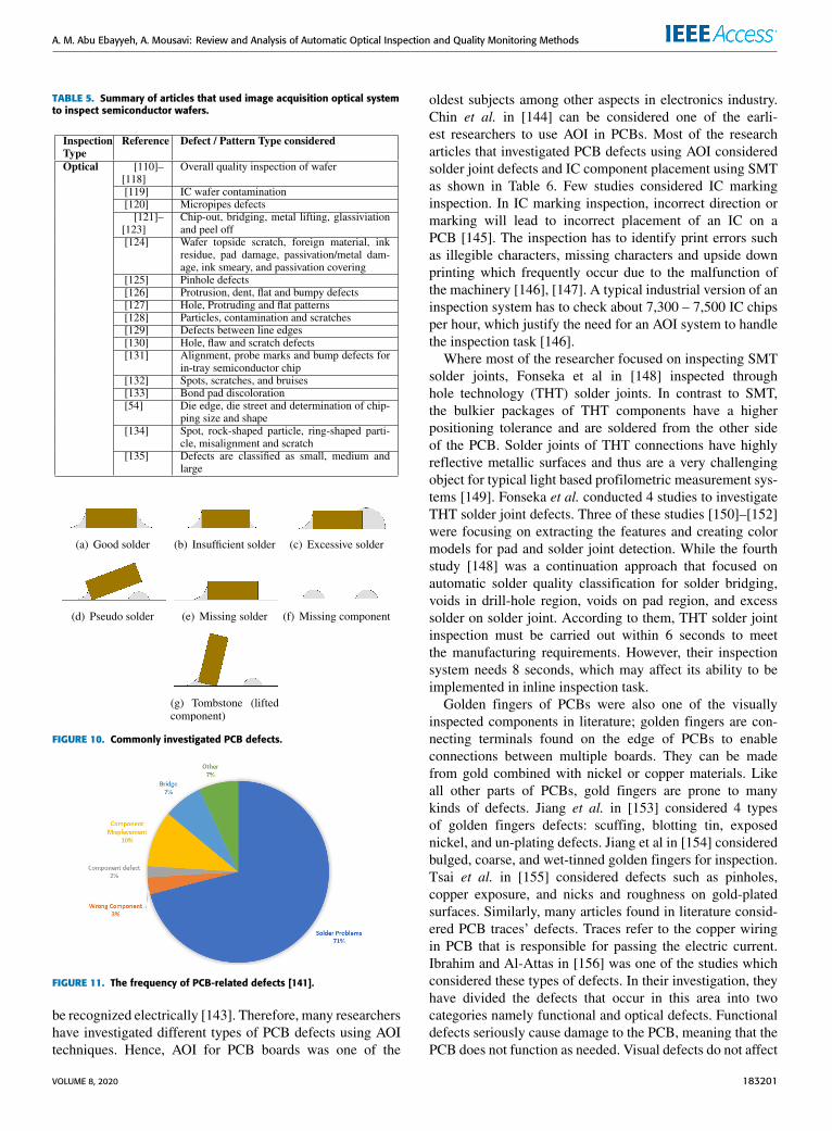
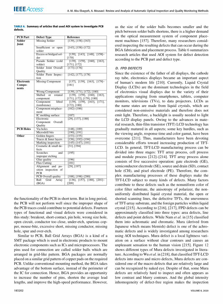
C. PCB DEFECTSIn recent years, demands for the placement of electronic com-ponents on PCBs at a higher density have increased [136].These components are assembled through electronic assem-bly lines which are applied in the manufacturing of allelectronic products such as TV, digital cameras, etc. Themainsteps in themanufacturing of PCB are the following: applyingsolder paste to PCB, placing IC on the board at correct posi-tions and placing the board in an oven to solder componentsto pads. [137]. During the manufacturing of PCBs, variousdefects may occur at each stage, most of them occur at sol-dering and component placement stages as shown in the piechart of Figure 11. For example, at the IC placing stage, defectcases of missing, wrong or doubled components may occur.In terms of possible soldering defects, most of them happenafter the reflowing stage, such as the defects at the IC packagecomponents (pseudo joint, excess solder, insufficient solder,shifting Solder and bridge defects) and the defects at thenon-IC components (side termination, tombstoned compo-nents, raised components, pseudo joint, excess solder, insuf-ficient solder, shifting, solder bridge) [138]. These defectscan severely affect the functionality of the PCB. For instance,a missing solder joint or insufficient solder joint can causean open circuit of the PCB and thus the overall functionalityof the circuit will be affected. Excess solder joint can causebridging with other PCB solder joints which can lead to ashort circuit. Pseudo solder (also known as cold solder) isconsidered a complex defect for detection [139]; this defectoccurs when the solder joint terminals are seemed to beconnected with the electronic component; however, there isno physical connection occurring which may lead to opencircuit contact. A pseudo joint is formed when insufficientheat is applied to completely melt the solder [140]. Figure 10shows commonly investigated defects in PCB industry.
TABLE 4. Summary of articles that used semi-optical system (circuitprobe) to produce WM for inspection.
Electric tests and manual vision inspection test are stillused; however, introducing surface mount technology (SMT)to the PCB assembly process made the PCB circuits muchfiner and more complex, which make the previously men-tioned defects more likely to occur and highlight the neces-sity of an AOI system [142]. In fact, it was proven thataround 80% of the optically recognizable defects could not
183200 VOLUME 8, 2020
A. M. Abu Ebayyeh, A. Mousavi: Review and Analysis of Automatic Optical Inspection and Quality Monitoring Methods
TABLE 5. Summary of articles that used image acquisition optical systemto inspect semiconductor wafers.
FIGURE 10. Commonly investigated PCB defects.
FIGURE 11. The frequency of PCB-related defects [141].
be recognized electrically [143]. Therefore, many researchershave investigated different types of PCB defects using AOItechniques. Hence, AOI for PCB boards was one of the
oldest subjects among other aspects in electronics industry.Chin et al. in [144] can be considered one of the earli-est researchers to use AOI in PCBs. Most of the researcharticles that investigated PCB defects using AOI consideredsolder joint defects and IC component placement using SMTas shown in Table 6. Few studies considered IC markinginspection. In IC marking inspection, incorrect direction ormarking will lead to incorrect placement of an IC on aPCB [145]. The inspection has to identify print errors suchas illegible characters, missing characters and upside downprinting which frequently occur due to the malfunction ofthe machinery [146], [147]. A typical industrial version of aninspection system has to check about 7,300 – 7,500 IC chipsper hour, which justify the need for an AOI system to handlethe inspection task [146].
Where most of the researcher focused on inspecting SMTsolder joints, Fonseka et al in [148] inspected throughhole technology (THT) solder joints. In contrast to SMT,the bulkier packages of THT components have a higherpositioning tolerance and are soldered from the other sideof the PCB. Solder joints of THT connections have highlyreflective metallic surfaces and thus are a very challengingobject for typical light based profilometric measurement sys-tems [149]. Fonseka et al. conducted 4 studies to investigateTHT solder joint defects. Three of these studies [150]–[152]were focusing on extracting the features and creating colormodels for pad and solder joint detection. While the fourthstudy [148] was a continuation approach that focused onautomatic solder quality classification for solder bridging,voids in drill-hole region, voids on pad region, and excesssolder on solder joint. According to them, THT solder jointinspection must be carried out within 6 seconds to meetthe manufacturing requirements. However, their inspectionsystem needs 8 seconds, which may affect its ability to beimplemented in inline inspection task.
Golden fingers of PCBs were also one of the visuallyinspected components in literature; golden fingers are con-necting terminals found on the edge of PCBs to enableconnections between multiple boards. They can be madefrom gold combined with nickel or copper materials. Likeall other parts of PCBs, gold fingers are prone to manykinds of defects. Jiang et al. in [153] considered 4 typesof golden fingers defects: scuffing, blotting tin, exposednickel, and un-plating defects. Jiang et al in [154] consideredbulged, coarse, and wet-tinned golden fingers for inspection.Tsai et al. in [155] considered defects such as pinholes,copper exposure, and nicks and roughness on gold-platedsurfaces. Similarly, many articles found in literature consid-ered PCB traces’ defects. Traces refer to the copper wiringin PCB that is responsible for passing the electric current.Ibrahim and Al-Attas in [156] was one of the studies whichconsidered these types of defects. In their investigation, theyhave divided the defects that occur in this area into twocategories namely functional and optical defects. Functionaldefects seriously cause damage to the PCB, meaning that thePCB does not function as needed. Visual defects do not affect
VOLUME 8, 2020 183201
A. M. Abu Ebayyeh, A. Mousavi: Review and Analysis of Automatic Optical Inspection and Quality Monitoring Methods
TABLE 6. Summary of articles that used AOI system to investigate PCBdefects.
the functionality of the PCB in short term. But in long period,the PCB will not perform well since the improper shape ofthe PCB traces could contribute to potential defects. Fourteentypes of functional and visual defects were considered inthis study: breakout, short-contact, pin hole, wrong size hole,open circuit, conductor too close, under-etch, spurious cop-per, mouse-bite, excessive short, missing conductor, missinghole, spur and over-etch.
Similar to PCB, Ball Grid Arrays (BGA) is a kind of aSMT package which is used in electronic products to mountelectronic components such as ICs and microprocessors. Thepins used for connection are called solder balls which arearranged in grid-like pattern. BGA packages are normallyplaced on a similar grid pattern of copper pads on the requiredPCB. Unlike conventional mounting method, the BGA takesadvantage of the bottom surface, instead of the perimeter ofthe IC for connection. Hence, BGA provides an opportunityto increase the number of pins, shorten the average leadlengths, and improve the high-speed performance. However,
as the size of the solder balls becomes smaller and thepitch between solder balls shortens, there is a higher demandon the optical measurement system of component place-ment machines [157]. Therefore, many researchers consid-ered inspecting the resulting defects that can occur during theBGA fabrication and placement process. Table 6 summarizesresearch articles that used AOI system for defect detectionaccording to the PCB part and defect type.
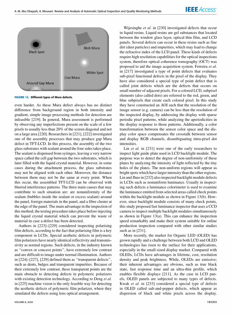
D. FPD DEFECTSSince the existence of the father of all displays, the cathoderay tube, electronics displays became an important aspectof human’s modern life [210]. Currently, Liquid CrystalDisplay (LCDs) are the dominant technologies in the fieldof electronics visual displays due to the variety of theirapplications ranging from smartphones, tablets, computermonitors, televisions (TVs), to data projectors. LCDs asthe name states are made from liquid crystals, which areconsidered non-emissive materials and therefore does notemit light. Therefore, a backlight is usually needed to lightthe LCD display panels. Owing to the advances in mate-rial research, thin-film transistor (TFT) LCD technology hasgradually matured in all aspects; some key hurdles, such asthe viewing angle, response time and color gamut, have beenovercome [211]. Thus, manufacturers have been devotingconsiderable efforts toward increasing production of TFT-LCD. In general, TFT-LCD manufacturing process can bedivided into three stages: TFT array process, cell processand module process [212]–[214]. TFT array process aloneconsists of five successive operation: gate electrode (GE),semiconductor electrode (SE), source and drain (SD), contacthole (CH), and pixel electrode (PE). Therefore, the com-plex manufacturing processes of these displays make theTFT-LCD subject to many kinds of defects. Many factorscontribute to these defects such as the nonuniform color ofcolor filter substrate, the anisotropy of polarizer, the non-uniformly distributed liquid crystal material, the open orshorted scanning lines, the defective TFTs, the unevennessof TFT-array substrate, and the foreign particles within liquidcrystal [215]. According to [216], [217], FPD defects can beapproximately classified into three types: area defects, linedefects and point defects. While Nam et al. in [15] classifiedthem into achromatic and chromatic. Mura (derived fromJapanese which means blemish) defect is one of the achro-matic defects and is widely investigated among researchersusing AOI techniques. Mura defect is a local lightness vari-ation on a surface without clear contours and causes anunpleasant sensation to the human vision [215]. Figure 12shows different types of Mura defects investigated in litera-ture. According toWu et al. in [218], that classified TFT-LCDdefects into macro and micro defects, Mura defects are con-sidered one of the macro defects that are relatively large andcan be recognized by naked eye. Despite of that, some Muradefects are relatively hard to inspect and often appears aslow contrast and blurry contours. And the global intensityinhomogeneity of defect-free region makes the inspection
183202 VOLUME 8, 2020
A. M. Abu Ebayyeh, A. Mousavi: Review and Analysis of Automatic Optical Inspection and Quality Monitoring Methods
FIGURE 12. Different types of Mura defects.
even harder. As these Mura defect always has no distinctdifference from background region in both intensity andgradient, simple image processing methods for detection areinfeasible [219]. In general, Mura assessment is performedby observing any imperfections present on the scale of a fewpixels to usually less than 20% of the screen diagonal and noton a large area [220]. Researchers in [221], [222] investigatedone of the assembly processes that may produce gap Muradefect in TFT-LCD. In this process, the assembly of the twoglass substrates with sealant around the four sides takes place.The sealant is dispensed from syringes, leaving a very narrowspace called the cell gap between the two substrates, which islater filled with the liquid crystal material. However, in somecases during the attachment process, the glass substratesmay not be aligned with each other. Moreover, the distancebetween them may not be the same at every point. Whenthis occur, the assembled TFT-LCD can be observed withblurred interference patterns. The three main causes that maycontribute to such situation are: are nonuniformity of thesealant (bubbles inside the sealant or excess sealant) aroundthe panel, foreign materials in the panel, and a fibre cluster atthe edge of the panel. The main advantage in the inspection ofthis method, the testing procedure takes place before injectingthe liquid crystal material which can prevent the waste ofmaterial in case a defect has been detected.
Authors in [223]–[229] considered inspecting polarisingfilm defects, according to the fact that polarising film is a keycomponent in LCDs. Special aesthetic defects in polymericfilm polarizers have nearly identical reflectivity and transmis-sivity as normal regions. Such defects, in the industry knownas ‘‘convex or concave points’’, have extremely low contrastand are difficult to image under normal illumination. Authorsin [224]–[227], [229] defined them as ‘‘transparent defects’’,such as dents, bulges and transparent impurities. Because oftheir extremely low contrast, these transparent points are themain obstacle to detecting defects in polymeric polarizerswith existing detection technology. According to Deng et al.in [225] machine vision is the only feasible way for detectingthe aesthetic defects of polymeric film polarizer, where theysimulated the defects using lens optical arrangement.
Wijesinghe et al. in [230] investigated defects that occurin liquid resins. Liquid resins are gel substances that locatedbetween the window glass layer, optical thin film, and LCDpanels. Several defects can occur in these resins such as finedirt (dust particles) and impurities, which may lead to changethe refractive index of the LCD panel. These kinds of defectsrequire high resolution capabilities for the optical inspectionssystem, therefore optical coherence tomography (OCT) wasproposed to aid the image acquisition system. Ferreira et al.in [217] investigated a type of point defects that evaluatessub-pixel functional defects in the pixel of the display. Theyhave also considered a special type of point defect that iscalled joint defects which are the defects that occurs onsmall number of adjacent pixels. For a colored LCD, subpixelelements (also called dots) are referred to the red, green, andblue subpixels that create each colored pixel. In this studythey have constructed an AOI such that the resolution of theimage sensor (e.g. camera) can be less than the resolution ofthe inspected display, by addressing the display with sparseperiodic pixel patterns, while analyzing the aperiodicities inthe display response to those patterns. Additionally, a colortransformation between the sensor color space and the dis-play color space compensates the crosstalk between sensorand display RGB channels, disambiguating intra-pixel dotintensities.
Lin et al. in [231] were one of the early researchers toinspect light guide plate used in LCD backlight module. Thepurpose was to detect the degree of non-uniformity of theseplates by analyzing the intensity of light reflected by the tinyholes of the plates. The non-uniform regions will appear asbright spots which have larger intensity than the other regions.Lin and Jhuo in [232] also inspected backlight module defectsin LCDs such as nonuniform luminance. Usually in inspect-ing such defects a luminance colorimeter is used to examinethe luminance emitted from selected areas called check pointswithin the backlight module as shown in Figure 13(b). How-ever, since backlight module consists of many check points,this study proposed fast luminance inspector that uses a CCDcamera to inspect multiple backlight modules simultaneouslyas shown in Figure 13(a). This can enhance the inspectionspeed remarkably and make their system suitable for onlineproduction inspection compared with other similar studiessuch as in [231].
More recently, the market for Organic LED (OLED) hasgrown rapidly and a challenge between both LCD and OLEDtechnologies has risen to the surface for their applications,especially in the small-sized display market. Compared withOLEDs, LCDs have advantages in lifetime, cost, resolutiondensity and peak brightness. While, OLEDs are emissive;their inherent advantages are obvious, such as true blackstate, fast response time and an ultra-thin profile, whichenables flexible displays [211]. As the case in LCD pan-els, OLED panels are subjected to many types of defects.Kwak et al. in [233] considered a special type of defectsin OLED called salt-and-pepper defects, which appear asdispersion of black and white pixels across the display.
VOLUME 8, 2020 183203

A. M. Abu Ebayyeh, A. Mousavi: Review and Analysis of Automatic Optical Inspection and Quality Monitoring Methods
FIGURE 13. LCD backlight module inspection [232].
This type of defects is caused by a malfunction in thechemical process and is considered difficult to detect usingconventional automatic fault detection methods that spe-cialize in recognizing certain shapes, such as line or Muradefects. Park and Kweon in [234] considered ambiguoussurface defects that are difficult to detect in active-matrixorganic light-emitting diode (AMOLED) touch displays. Dif-ferent types of ambiguous defects were considered in thisstudy such as scratch, long dust, circle dust, pit and stain.This paper highlighted some problems in inspecting suchdefects, such as confusing critical and non-critical defects.For instance, dust defect which is considered non-criticaldefects because it can be removed easily can be confused withscratch which is considered a critical defect. Authors in [235],[236] proposed AOI system that can detect defect in direc-tional surface defects in general. To validate the efficiencyof their system, they conducted experimental trials on defec-tive and non-defective samples of polymer light-emittingdiode (PLED) and OLED.
Table 7 summarizes the defects investigated in literatureusing AOI system for different FPD types.
E. OTHER DEFECTSIn the previous sections (III-A-III-D) we discussed about themost common inspected components in literature in a catego-rizedmanner. However, other researchers have studied certainelectronic component defects that are not widely investigated.For instance, Ko et al. in [289] inspected four types of defectsin complementarymetal-oxide-semiconductor (CMOS) cam-era module named black and white defect, dim defect, colordefect, and line defects. Their method achieved an overallof 99.6% inspection accuracy. However, they chose differentinspection algorithms for each type of defect inspected, whichreduce the efficiency of their method to deal with new defect
TABLE 7. Summary of articles that used AOI system to investigate FPDdefects.
types and increase the complexity and time consumption.Furthermore, particles in the range of 2 – 3 pixels werenot accurately detected. Infrared Cut-off (IR-CUT) filter inCMOS and charge-coupled device (CCD) cameras is also oneof the investigated components in literature. IR-CUT filter isdesigned to reflect or block mid-infrared wavelengths whilepassing visible light. It is applied in all kinds of color camerasand video devices to prevent infrared light radiation fromreaching imaging sensor, in an attempt to capture imagesas close to those perceived by the human eye as possible.Defects in this part can affect quality of the image, throughchromatic aberration phenomenon and redundant objects inthe image. Therefore, Liu and Yu in [290] proposed an AOIsystem to investigate three types of common surface defectsin IR-CUT filter: stain, scratch, and edge crack. Stain iscaused by the dirt in the air or dirty objects in contact with
183204 VOLUME 8, 2020

A. M. Abu Ebayyeh, A. Mousavi: Review and Analysis of Automatic Optical Inspection and Quality Monitoring Methods
it. The cleaning and testing process of optical IR-CUT filtermay bring scratches on the surface by contact with sharpthings such as tweezers. Crack is generated in the process ofsegmentation after coating.
Lin et al. in [291], [292] considered inspecting rip-ple defects in the surface barrier layer chips of ceramiccapacitors. Difficulties exist in automatically inspecting rip-ple defects because of their semi-opaque and unstructuredappearances, the gradual changes of their intensity levels,and the low intensity contrast between their surfaces andthe rough exterior of a the chip as shown in Figure 14.To overcome these difficulties the sample image has tobe converted to the frequency domain in order to capturethe defect features as will be explained in section V-B1.Sun et al. in [293] considered inspecting four types of thermalfuses defects. A thermal fuse, also known as a thermal cut-off,is an important component in both electrical and electronicdevices. Thermal fuses prevent circuits from overheatingor becoming overloaded. While fuses generally allow thepassage of current, they can short circuit to cut power toappliances as a safety feature. The four inspected defects inthis study are located on the head of the thermal fuse whichare bur, black dot, small-head, and flake defects. Bur defect(Figure 15(a)) appears as a deckle edge in the outer ringarea of the fuse case, it is mainly caused by using incorrectmaterial for the lead or worn out punch. This defect is verydifficult to be detected by human inspector even with thehelp of magnifier. Black dot defect (Figure 15(b)) is mainlycaused by the existence of foreign materials (e.g. dirt or dust)during the assembly of the case and lead. Small-head defects(Figure 15(c)) occurs when insufficient force is provided dur-ing the punching process of the lead, this will cause smallerdimension of the head diameter. Flake defects (Figure 15(d))is caused by the chip-off of the case wall during the electro-plating process.
FIGURE 14. Example of ripple defect investigated in [291], [292].
Table 8 summarizes miscellaneous defects that were inves-tigated using AOI techniques.
IV. IMAGE ACQUISITION TECHNOLOGIES - HARDWARESYSTEMSAn effective imagery system should ensure minimum escaperates and false alarms [300]. Image quality is an essential
FIGURE 15. Defects of thermal fuse. a Bur, b black-dot, c small-head,dflake [293].
TABLE 8. Summary of articles that used AOI system to investigatemiscellaneous electronic components defects.
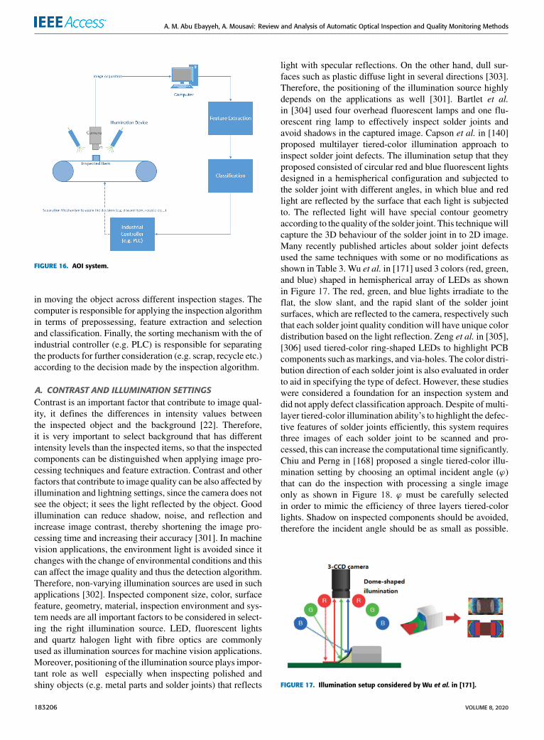
prerequisite for data acquisition and processing. Therefore,a careful consideration should be made for the selection ofappropriate image acquisition system. According to Chin andHarlow in [13], a standard AOI system consists of cameraand lightning setup, computer (processor), conveyor and sort-ing mechanism as shown in Figure 16. The illumination isresponsible for providing constant/customized lightning con-ditions. The camera that includes an image sensor is respon-sible in acquiring the image. The conveyor is responsible
VOLUME 8, 2020 183205
A. M. Abu Ebayyeh, A. Mousavi: Review and Analysis of Automatic Optical Inspection and Quality Monitoring Methods
FIGURE 16. AOI system.
in moving the object across different inspection stages. Thecomputer is responsible for applying the inspection algorithmin terms of prepossessing, feature extraction and selectionand classification. Finally, the sorting mechanism with the ofindustrial controller (e.g. PLC) is responsible for separatingthe products for further consideration (e.g. scrap, recycle etc.)according to the decision made by the inspection algorithm.
A. CONTRAST AND ILLUMINATION SETTINGSContrast is an important factor that contribute to image qual-ity, it defines the differences in intensity values betweenthe inspected object and the background [22]. Therefore,it is very important to select background that has differentintensity levels than the inspected items, so that the inspectedcomponents can be distinguished when applying image pro-cessing techniques and feature extraction. Contrast and otherfactors that contribute to image quality can be also affected byillumination and lightning settings, since the camera does notsee the object; it sees the light reflected by the object. Goodillumination can reduce shadow, noise, and reflection andincrease image contrast, thereby shortening the image pro-cessing time and increasing their accuracy [301]. In machinevision applications, the environment light is avoided since itchanges with the change of environmental conditions and thiscan affect the image quality and thus the detection algorithm.Therefore, non-varying illumination sources are used in suchapplications [302]. Inspected component size, color, surfacefeature, geometry, material, inspection environment and sys-tem needs are all important factors to be considered in select-ing the right illumination source. LED, fluorescent lightsand quartz halogen light with fibre optics are commonlyused as illumination sources for machine vision applications.Moreover, positioning of the illumination source plays impor-tant role as well especially when inspecting polished andshiny objects (e.g. metal parts and solder joints) that reflects
light with specular reflections. On the other hand, dull sur-faces such as plastic diffuse light in several directions [303].Therefore, the positioning of the illumination source highlydepends on the applications as well [301]. Bartlet et al.in [304] used four overhead fluorescent lamps and one flu-orescent ring lamp to effectively inspect solder joints andavoid shadows in the captured image. Capson et al. in [140]proposed multilayer tiered-color illumination approach toinspect solder joint defects. The illumination setup that theyproposed consisted of circular red and blue fluorescent lightsdesigned in a hemispherical configuration and subjected tothe solder joint with different angles, in which blue and redlight are reflected by the surface that each light is subjectedto. The reflected light will have special contour geometryaccording to the quality of the solder joint. This techniquewillcapture the 3D behaviour of the solder joint in to 2D image.Many recently published articles about solder joint defectsused the same techniques with some or no modifications asshown in Table 3. Wu et al. in [171] used 3 colors (red, green,and blue) shaped in hemispherical array of LEDs as shownin Figure 17. The red, green, and blue lights irradiate to theflat, the slow slant, and the rapid slant of the solder jointsurfaces, which are reflected to the camera, respectively suchthat each solder joint quality condition will have unique colordistribution based on the light reflection. Zeng et al. in [305],[306] used tiered-color ring-shaped LEDs to highlight PCBcomponents such asmarkings, and via-holes. The color distri-bution direction of each solder joint is also evaluated in orderto aid in specifying the type of defect. However, these studieswere considered a foundation for an inspection system anddid not apply defect classification approach. Despite of multi-layer tiered-color illumination ability’s to highlight the defec-tive features of solder joints efficiently, this system requiresthree images of each solder joint to be scanned and pro-cessed, this can increase the computational time significantly.Chiu and Perng in [168] proposed a single tiered-color illu-mination setting by choosing an optimal incident angle (ϕ)that can do the inspection with processing a single imageonly as shown in Figure 18. ϕ must be carefully selectedin order to mimic the efficiency of three layers tiered-colorlights. Shadow on inspected components should be avoided,therefore the incident angle should be as small as possible.
FIGURE 17. Illumination setup considered by Wu et al. in [171].
183206 VOLUME 8, 2020
A. M. Abu Ebayyeh, A. Mousavi: Review and Analysis of Automatic Optical Inspection and Quality Monitoring Methods
FIGURE 18. Illumination setup considered by Chiu et al. in [168].
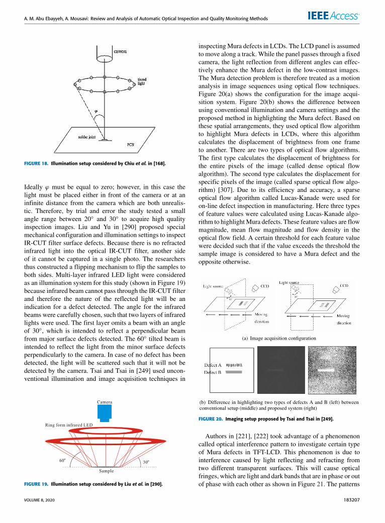
Ideally ϕ must be equal to zero; however, in this case thelight must be placed either in front of the camera or at aninfinite distance from the camera which are both unrealis-tic. Therefore, by trial and error the study tested a smallangle range between 20◦ and 30◦ to acquire high qualityinspection images. Liu and Yu in [290] proposed specialmechanical configuration and illumination settings to inspectIR-CUT filter surface defects. Because there is no refractedinfrared light into the optical IR-CUT filter, another sideof it cannot be captured in a single photo. The researchersthus constructed a flipping mechanism to flip the samples toboth sides. Multi-layer infrared LED light were consideredas an illumination system for this study (shown in Figure 19)because infrared beam cannot pass through the IR-CUT filterand therefore the nature of the reflected light will be anindication for a defect detected. The angle for the infraredbeams were carefully chosen, such that two layers of infraredlights were used. The first layer omits a beam with an angleof 30◦, which is intended to reflect a perpendicular beamfrom major surface defects detected. The 60◦ tilted beam isintended to reflect the light from the minor surface defectsperpendicularly to the camera. In case of no defect has beendetected, the light will be scattered such that it will not bedetected by the camera. Tsai and Tsai in [249] used uncon-ventional illumination and image acquisition techniques in
FIGURE 19. Illumination setup considered by Liu et al. in [290].
inspecting Mura defects in LCDs. The LCD panel is assumedto move along a track. While the panel passes through a fixedcamera, the light reflection from different angles can effec-tively enhance the Mura defect in the low-contrast images.The Mura detection problem is therefore treated as a motionanalysis in image sequences using optical flow techniques.Figure 20(a) shows the configuration for the image acqui-sition system. Figure 20(b) shows the difference betweenusing conventional illumination and camera settings and theproposed method in highlighting the Mura defect. Based onthese spatial arrangements, they used optical flow algorithmto highlight Mura defects in LCDs, where this algorithmcalculates the displacement of brightness from one frameto another. There are two types of optical flow algorithms.The first type calculates the displacement of brightness forthe entire pixels of the image (called dense optical flowalgorithm). The second type calculates the displacement forspecific pixels of the image (called sparse optical flow algo-rithm) [307]. Due to its efficiency and accuracy, a sparseoptical flow algorithm called Lucas-Kanade were used foron-line defect inspection in manufacturing. Here three typesof feature values were calculated using Lucas-Kanade algo-rithm to highlightMura defects. These feature values are flowmagnitude, mean flow magnitude and flow density in theoptical flow field. A certain threshold for each feature valuewere decided such that if the value exceeds the threshold thesample image is considered to have a Mura defect and theopposite otherwise.
FIGURE 20. Imaging setup proposed by Tsai and Tsai in [249].
Authors in [221], [222] took advantage of a phenomenoncalled optical interference pattern to investigate certain typeof Mura defects in TFT-LCD. This phenomenon is due tointerference caused by light reflecting and refracting fromtwo different transparent surfaces. This will cause opticalfringes, which are light and dark bands that are in phase or outof phase with each other as shown in Figure 21. The patterns
VOLUME 8, 2020 183207
A. M. Abu Ebayyeh, A. Mousavi: Review and Analysis of Automatic Optical Inspection and Quality Monitoring Methods
FIGURE 21. Illumination setup proposed in [221], [222].
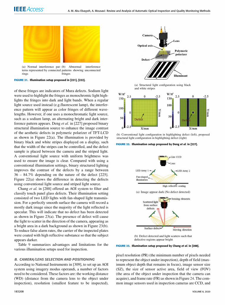
of these fringes are indicators of Mura defects. Sodium lightwere used to highlight the fringes as monochromic light high-lights the fringes into dark and light bands. When a regularlight source used instead (e.g.fluorescent lamp), the interfer-ence pattern will appear as color fringes of different wave-lengths. However, if one uses a monochromatic light source,such as a sodium lamp, an alternating bright and dark inter-ference pattern appears. Deng et al. in [227] proposed binarystructural illumination source to enhance the image contrastof the aesthetic defects in polymeric polarizer of TFT-LCDas shown in Figure 22(a). The illumination is provided bybinary black and white stripes displayed on a display, suchthat the width of the stripes can be controlled, and the defectsample is placed between the camera and the striped light.A conventional light source with uniform brightness wasused to ensure the image is clear. Compared with using aconventional illumination settings, binary structured lightingimproves the contrast of the defects by a range between36 – 84.7% depending on the nature of the defect [225].Figure 22(a) shows the difference in detecting the defectsusing conventional light source and striped light source.
Chang et al. in [288] offered an AOI system to filter andclassify touch panel glass defects. Their illumination settingconsisted of two LED lights with fan-shaped light transmis-sion. For a perfectly smooth surface the camera will record amostly dark image since the majority of the light reflected isspecular. This will indicate that no defect has been detectedas shown in Figure 23(a). The presence of defect will causethe light to scatter in the direction of the camera, appearing asa bright area in a dark background as shown in Figure 23(b).To reduce false alarm rates, the carrier of the inspected plateswere coated with high reflective substance so that the subjectappears darker.
Table 9 summarizes advantages and limitations for thevarious illumination setups used for inspection.
B. CAMERA/LENS SELECTION AND POSITIONINGAccording to National Instruments in [309], to set up an AOIsystem using imagery modus operandi, a number of factorsneed to be considered. These factors are: the working distance(WD) (distance from the camera lens to the object underinspection), resolution (smallest feature to be inspected),
FIGURE 22. Illumination setup proposed by Deng et al. in [227].
FIGURE 23. Illumination setup proposed by Chang et al. in [288].
pixel resolution (PR) (the minimum number of pixels neededto represent the object under inspection), depth of field (max-imum object depth that remains in focus), image sensor size(SZ), the size of sensor active area, field of view (FOV)(the area of the object under inspection that the camera canacquire), and frame rate (FR) as shown in Figure 24. The com-mon image sensors used in inspection cameras are CCD, and
183208 VOLUME 8, 2020
A. M. Abu Ebayyeh, A. Mousavi: Review and Analysis of Automatic Optical Inspection and Quality Monitoring Methods
TABLE 9. Summary for illumination systems used in AOI applications.
CMOS which mimics human’s perception in vision [310].In addition to the previous factors several criteria are con-sidered in determining the suitable image sensor and its sizesuch as responsivity, dynamic range, uniformity, speed ofoperation and reliability. Using the field of view (FOV),
the pixel resolution can be obtained by equation 1
PR = 2 ·(
FOVResolution
)(1)
VOLUME 8, 2020 183209

A. M. Abu Ebayyeh, A. Mousavi: Review and Analysis of Automatic Optical Inspection and Quality Monitoring Methods
And the focal length, which is used to determine the lensspecifications, can be obtained using equation 2
FL =SZ ·WDFOV
(2)
Focal length is important for selecting the right lens forapplication, as can be seen from equation 2, the three factorsthat affect selection of right focal length are sensor size, work-ing distance and field of view. Frame rate is also importantfactor to consider when selecting a camera especially in batchinspection in industries that have high production rate [303].
Spatial calibration techniques are commonly used in orderto set the camera in optimal position for the application.In most optical inspection applications, the position of thecamera is fixed [300] and positioned in 90◦ with the plane ofinspected components to avoid image distortion and reduceperspective errors as shown in Figure 24 [309]. However,in some cases the camera can be aligned in different angles.In the following discussion, we will highlight the researcharticles that used unconventional camera setups.
FIGURE 24. Factors considered in selecting camera and lens [309].
For inspecting glass substrate defects in TFT-LCD, cam-eras are aligned in two different positions: transmission andreflection. In transmission position the camera captures theprojected images with light transmitting through the glass
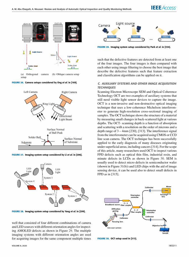
whereas in the reflection position it captures the reflectedimages with light reflecting off the substrates as shownin Figure 25 [263]. Hence, Yousefian-Jazi et al. in [263]used the transmission method for inspecting TFT-LCD glasssubstrates. Similar techniques are considered when inspect-ing highly reflective surfaces, in which certain geometri-cal laws must be applied to measure the optimum lengthsand angles of the camera and illumination settings [311].Ong et al. in [169] proposed dual viewing angle to acquiresolder joint images for defects inspection. Their approachconsisted of conventional orthogonal and oblique camerasetups as shown in Figure 26. The oblique setup was adjustedwith inclined viewing direction of 40◦ by using pyramid mir-ror. The setting seems to provide better geometrical informa-tion of the solder joint and can save feature extractions step bysending the acquired images directly for classification. How-ever, the setup procedure is laborious and prone to humanerror. Li et al. in [206] proposed a setup for detecting theheight of solder balls in BGA. They used stereo vision systemto capture the 3D nature of the solder ball using two CCDcameras at two opposing angles and two ring lights aroundeach camera lens that captures two 2D images in parallel asshown in Figure 27. Because of the reflective nature of solderballs, the lighting provides the means to generate featureson the balls which are then used to determine height. Thesefeatures will appear as bright regions in the captured images.This method of acquiring image can reduce the time for thefeature extraction process such as simple segmentation andthresholding approaches are enough to determine the featuresof the component. Zhao et al. in [312] proposed a similarstereo vision system using two cameras to inspect the pinson multi-type electrical connectors of the components.
FIGURE 25. (a) transmission and (b) reflection imaging system [263].
Because each film capacitor has six surfaces to be detected,Yang et al. in [299] used four image acquisition systems thatare adjusted to detect the surface defects of capacitors. Eachcamera gets the image information of two surfaces from sideangle, as shown in Figure 28. When the capacitor reaches thespecified position, a laser tube will number the capacitor andproduce trigger signal. Industrial camera captures the surfaceimage of this capacitor and optical inspection algorithms areapplied to detect the surface defects in real time. Park andKweon in [234] proposed four image acquisition systems as
183210 VOLUME 8, 2020
A. M. Abu Ebayyeh, A. Mousavi: Review and Analysis of Automatic Optical Inspection and Quality Monitoring Methods
FIGURE 26. Camera setups considered by Ong et al. in [169].
FIGURE 27. Imaging system setup considered by Li et al. in [206].
FIGURE 28. Imaging system setup considered by Yang et al. in [299].
well that consisted of four different combinations of cameraand LED sources with different orientation angles for inspect-ing AMOLED defects as shown in Figure 29. The multipleimaging systems with different orientation angles are usedfor acquiring images for the same component multiple times
FIGURE 29. Imaging system setup considered by Park et al. in [234].
such that the defective features are detected from at least oneof the four images. The four images is then compared witheach other using image filtering to choose the best image thatdescribe the defective features such that feature extractionand classification algorithms can be applied on it.
C. AUXILIARY SYSTEMS AND OTHER IMAGE ACQUISITIONTECHNIQUESScanning Electron Microscope SEM and Optical CoherenceTechnology OCT are two examples of auxiliary systems thatstill need visible light sensor devices to capture the image.OCT is a non-invasive and non-destructive optical imagingtechnique that uses a low-coherence Michelson interferom-eter to generate high-resolution cross-sectional imaging ofsamples. TheOCT technique shows the structure of amaterialby measuring small changes in back-scattered light at variousdepths. The OCT- scanning depth is a function of absorptionand scattering with a resolution on the order of microns and adepth range of 3 – 4mm [230], [313]. The interference signalfrom the interferometer can be acquired using CMOS or CCDline scan camera. The OCT technique has been successfullyapplied to the early diagnosis of many diseases originatingunder superficial areas, including cancers [314]. For the scopeof this article, many researchers used OCT to inspect variousFPD defects such as optical thin film, industrial resin, andminute defects in LCDs as shown in Figure 30. SEM isusually used to detect micro defects in semiconductor wafer(shown in Figure 31(b)) and LED chips with the aid of imagesensing device, it can be used also to detect small defects inFPD as in [315].
FIGURE 30. OCT setup used in [313].
VOLUME 8, 2020 183211
A. M. Abu Ebayyeh, A. Mousavi: Review and Analysis of Automatic Optical Inspection and Quality Monitoring Methods
FIGURE 31. Various semiconductor wafer testing techniques.
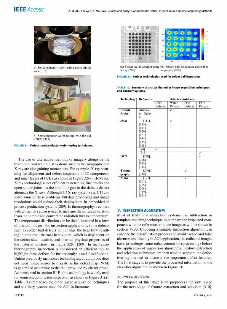
The use of alternative methods of imagery alongside thetraditional surface optical systems such as thermography andX-ray are also gaining momentum. For example, X-ray scan-ning for alignment and defect inspection of IC componentsand inner layers of PCBs as shown in Figure 32(a). However,X-ray technology is not efficient in detecting fine cracks andopen solder joints, as the small air gap in the defects do notattenuate theX-rays. Although 3DX-ray system (e.g. CT) cansolve some of these problems, but data processing and imageresolutions could reduce their deployment in embedded inprocess production systems [209]. In thermography, a camerawith a thermal sensor is used to measure the infrared radiationfrom the sample and convert the radiation flux to temperature.The temperature distribution can be then illustrated in a formof thermal images. For inspection applications, some defectssuch as solder ball defects will change the heat flow result-ing in abnormal thermal behaviours, which is dependent onthe defect size, location, and thermal physical properties ofthe material as shown in Figure 32(b) [209]. In such casesthermography inspection is considered an efficient tool tohighlight these defects for further analysis and classification.Unlike previously mentioned technologies, circuit probe doesnot need image sensor to operate as the defect map (WM)is generated according to the data provided by circuit probe.As mentioned in section III-B, this technology is widely usedfor semiconductor wafer inspection as shown in Figure 31(a).Table 10 summarizes the other image acquisition techniquesand auxiliary systems used for AOI in literature.
FIGURE 32. Various technologies used for solder ball inspection.
TABLE 10. Summary of articles that other image acquisition techniquesand auxiliary systems.
V. INSPECTION ALGORITHMMost of traditional inspection systems use subtraction ortemplate matching technique to compare the inspected com-ponent with the reference template image as will be shown insection V-B3. Choosing a suitable inspection algorithm canenhance the classification process and avoid escape and falsealarms rates. Usually in AOI application, the collected imageshave to undergo some enhancement (preprocessing) beforethe application of inspection algorithms. Feature extractionand selection techniques are then used to segment the defec-tive regions and to discover the important defect features.The final stage is to provide the processed information to theclassifier algorithm as shown in Figure 16.
A. PREPROCESSINGThe purpose of this stage is to preprocess the raw imagefor the next stage of feature extraction and selection [310].
183212 VOLUME 8, 2020
A. M. Abu Ebayyeh, A. Mousavi: Review and Analysis of Automatic Optical Inspection and Quality Monitoring Methods
This stage involves many operations such as image mask-ing, spatial filtering and geometric transformations. Maskingoperations can be applied to the acquired image in order todefine the region of interest (ROI). This step is very importantin reducing the inspection time such that the feature extrac-tion is only applied into certain region instead of the entireimage. After specifying the ROI, the resulting image can besubjected to geometric transformation or/and filtering for fur-ther enhancement before applying the inspection algorithm.Geometric transformation involves calculating the projectionof each pixel in the ROI onto another space. This method canhelp in image restoration and correction in case of any pres-ence of geometric distortion. The geometric transformationincludes scaling, rotating and translation of the image [189].
Image denoising and filtering are common practices in pre-processing acquired images before using feature extractionalgorithms. The process of image data filtering and denoisingreduces noise and enhances the data for highlighting theimportant features. They can smooth, sharpen, transform, andremove noise from the image, so that the inspection algorithmcan do the feature extraction task easily. For instance, imagefiltering and denoising techniques are very useful in removingrandom defects from mixed patterns WM so that classifica-tion algorithms can specify the type of defect according tothe systematic pattern [109]. The mathematical applicationof filters can be in form of linear or non-linear. In the case oflinear filters, a convolution kernel is specified, it can be square(e.g. 3 × 3), or a rectangle (e.g. 3 × 5). Examples of linearfilters are Laplacian, and Gaussian filters. Non-linear filtersuse non-linear functions for the parameters of the kernel,the process of recalculating the pixel is similar as in the linearfilters. Some examples of nonlinear filters are median filtersand Prewitt filter. Median filters are popular preprocessingmethod for abnormality detection in electronic device inspec-tion applications [71]. More advanced denoising techniquessuch as deep learning models [322], low rank approxima-tion [323], and weighted nuclear norm minimization [324]are also used in literature. Park and Kweon in [234] proposednovel filtering technique called neighboring difference fil-ter (NDF) from the background of AMOLED sample images.NDF is used to compare the intensity of neighboring pixelregions with a strategically placed gap space to differentiatesimilar patterns from other (i.e. abnormality detection).
B. FEATURE EXTRACTION AND SELECTIONFeature extraction process involves applying one or moreof image processing techniques (e.g. frequency analysis andsegmentation) in order to describe the characteristics of thestudied regions (e.g. defects and abnormalities). These char-acteristics are usually described using a set of values calledFeature Values that can be represented in vector or matrixform. The purpose of feature selection step is to consider theimportant feature values only that can contribute to the clas-sification process and discard the redundant ones. This stepis very essential in reducing the computational time for theinspection algorithm. Principle Component Analysis is very
popular technique used in feature selection. Other algorithmssuch as along Genetic Algorithm (GA), Particle Swarm Opti-mization (PSO), Ant Colony Optimization (ACO), Adaboostand Neural Networks are also used for this purpose.
1) FREQUENCY DOMAIN ANALYSISFrequency domain analysis can be used to convert picturesfrom the spatial domain to the frequency domain. This isvery useful for capturing the global structure of the imageand minimising reconstruction errors. In frequency analysis,high pass and low pass frequency filters can be used to atten-uate the unnecessary noise in the image. After attenuation,the picture can be transformed back to the spatial domain forfurther processing. Frequency analysis is preferably used ininvestigating defects that have low contrast and high illumina-tion noise such that spatial domain cannot capture the featuresof the defect. Examples of defects that have these featuresare Mura defects shown in Figure 12, and ripple defects inceramic capacitors shown in Figure 14. The frequency repre-sentation can be obtained by various transform functions suchas Fast Fourier Transform (FFT), DiscreteWavelet Transform(DWT), and Discreet Cosine Transform (DCT). Transformfunctions allows for a noninvertible transformation from thespatial domain to a reduced dimensionality feature space.Thus, facilitating classification with substantially less fea-tures and manageable classification error.
DCT is mainly applied to perform image reconstructionand dimension reduction by converting the image to a fre-quency spectrum and attenuates certain coefficients that laysinto two major bands, namely, low frequency, and highfrequency [125]. In most AOI applications, since illumi-nation variations mainly lie in the low-frequency band (inupper-left corner of the frequency spectrum), an appropriatenumber of DCT coefficients in low-frequency band are trun-cated to minimize variations under different lighting condi-tions as shown in Figure 33 [161]. Chen and Kuo in [240]applied DCT and background image filtering strategy todetect Mura defects in TFT-LCD. The background of thesample images was first located and reconstructed using theDCT approach with the aid of low-pass filtering to illuminateunwanted noise. DCT coefficients are then selected and
FIGURE 33. Truncating lower frequency coefficient (C00).
VOLUME 8, 2020 183213
A. M. Abu Ebayyeh, A. Mousavi: Review and Analysis of Automatic Optical Inspection and Quality Monitoring Methods
the image can be transformed back to the spatial domainusing inverse DCT. The Mura defects can be then sub-tracted from the background using image subtraction method.Despite the slight difference in brightness and non-uniformitybetween blob-Mura defects and the background, the proposedapproach is very efficient in detecting blob-Mura defectsas well. However, because of the low-pass filtering stepconducted, micro defects can be eliminated with the noise.Therefore, the approach proposed cannot handle detectingmicro-defects in TFT-LCD. Even if it was modified to detectmicro-defect, the computational time of the process will belengthy. Perng and Chen in [236] used DCT to highlight thedefective features directional textured surfaces in FPD suchas PLED and OLED. The sample images were transformed tothe frequency domain using DCT so that the dominant direc-tions of the textures are compacted with the lower frequencyband coefficients of the frequency image. The linear primi-tives associated with high energy in the DCT domain are theneliminated by reducing them to zero. After that, the image istransformed back to the spatial domain using inverse DCT,which makes the defective features visible. Thresholding andStatistical Process Control (SPC) chart were then used toclassify the defects. Several advantages were observed usingthis approach such that it is insensitive to horizontal andvertical shifting, changes in illumination, and image rotation.However, this study did not provide any details about theaccuracy of the proposed approach nor of the computationaltime consumed. Similarly, Lin in [298] used DCT to inves-tigate tiny surface defects in Surface Barrier Layer found inpassive electronic components, whose random surface texturecontains no repetitions of basic texture primitives. Therefore,DCT approach is well suited to be applied in this problemsince it does not require any textural feature information. Theproposed method achieved a relatively high overall accuracyof 94.74%. However, this method is only suitable to detectdefects in the range between two to fourteen pixels. Further-more, this method is considered time consuming since it takesfour seconds only to apply forward and inverse DCT withoutthe classification takes place. Lin and Chiu in [38], [40]used Block discrete cosine transform (BDCT) to highlightthe defected features of tiny surface flaws in epoxy domesof LEDs and blemishes of curved LED lenses respectively.BDCT method is similar to DCT; however, in BDCT theimage is divided into non-overlapping image blocks of equalsizes which DCT can take place in each block separatelyinstead of applying DCT to the whole image. In both studiesit was found that the dark background of the image can affectthe BDCT and can be confused with the defect features.Therefore, after specifying the ROI, an image mask is used todelineate the ROI. Since BDCT can only process rectangularregions and the ROI is circular, therefore the dark backgroundthat has been removed can be replaced with a backgroundthat has duplicated average gray level of the ROI. Unevenself-illumination lighting will result in gradual shades, whichwill cause high frequency peaks after performing BDCT.Therefore, gray relational analysis is used to attenuate the
high frequency values then transform the image again to thespatial domain after the attenuation. Otsu-thresolding werethen used to transform the resulted image into digital imagewith highlighted flaws being detected. Lin and Ho in [125]found that after transforming the digital image of a chip ina wafer to the DCT domain, the frequencies of the pinholedefects spread around the middle and high frequency regions.Therefore, to highlight pinhole defects features, high passfiltering where used to attenuate the frequency components ofthe non-defect regions by setting their values to zero. Similarto the approaches that were conducted in [38], [40] to adaptthe background for DCT implementing, the proposed methodwere insensitive to light variations, since the low frequencyband has been eliminated. However, this method has somelimitations such as defect size, background property and pro-cessing time. Defects of large size features can be lost afterthe attenuation of low frequency band. Moreover, defectsembedded in structure textures cannot be detected becausethis method is suitably applied to identify defects in randomtextures. Finally, the proposed method takes four seconds toprocess a forward and an inverse DCT transformation, whichcould not meet the requirements of an on-line inspectionssystem.
As mentioned earlier that DWT is one of the frequencydomain analysis methods for feature extraction. DWT hasthe advantage of providing an easy way for multi-resolutionrepresentation, from which defect texture features can beeasily extracted. The merits of using DWT include localimage processing, simple calculations, high speed processingand multiple image information. Lin in [36] considered onetype of wavelet transform called Haar transform to highlightwater-drop defects on LED chip surface. Haar transform isconsidered the simplest approach among wavelet transforms.The transform is performed to each row of pixel values andthen performing another wavelet transform to each column.Four wavelet transforms were used that generate four sub-images; one level of wavelet decomposition generates onesmooth sub-image and three detail sub-images that containfine structures with horizontal, vertical and diagonal orienta-tions. Each sub-image represents certain characteristic thathas half the number of columns and rows of the originalimage. Wu et al. in [218] used Fourier transform to high-light the micro-defects of TFT-LCD by removing backgroundtextures. Haar-wavelet transform were also used to eliminatethe influence of uneven illumination. Ferreira et al. in [217]took advantage of the periodicity and used Fourier filter-ing technique with the aid of thresholding to highlight dotsdefects in FPDs. The factor that was under scope in thisstudy was the luminous intensity of dots, such that defectivedots may be identified by changes in the expected lightfunctional response to their addressing digital value. Themain advantage of this study that it was able to constructan AOI system using a camera that can have lower reso-lution of that in the display inspected. However, there arerestrictions in detecting defects using the Fourier transformwhen the frequency component of a defect may not have a
183214 VOLUME 8, 2020

A. M. Abu Ebayyeh, A. Mousavi: Review and Analysis of Automatic Optical Inspection and Quality Monitoring Methods
repeated pattern [260]. Tsai and Hung in [251] proposed asystem based on Fourier reconstruction and wavelet trans-form for inspectingmicro-defects such as pinholes, scratches,and particles in TFT-LCD. This study works on the 1Dline images instead of the traditional two-dimensional areaimages. Unwanted frequency components, which representthe periodic structural pattern of the image in the frequencyspectrum, can be eliminated. Using inverse Fourier transform,the image can be transformed back to the spatial domain.Finally, wavelet decomposition is further applied to removeuneven illumination in the filtered image so that defects canbe easily segmented for the classification process. Controllimits were considered for the classification process usingcertain threshold to distinguish between anomalies and uni-form background. In similar study [252], Tsai et al. conducteda slightly different approach in which the segmented 1Dprofile image is divided into small segments, each of thelength of the repeated period for a given TFT-LCD panel.The divided 1D segments are then combined as a 2D image.Then the same procedure applies on the 2D image as it wason the 1D image in the previous study. Another differencein this study, that it did not use wavelet transform. Theproposed methods have main advantage of not relying onthe design of quantitative features to describe various defecttypes, nor require a template image for comparison. Thus,they alleviate all limitations of the feature extraction and tem-plate matching methods. However, several drawbacks wereobserved in [252] such as the periodic of a faultless scanline cannot be effectively removed since the number of thedivided segments is generally small with respect to the lengthof the period in a scan line. Furthermore, themethod proposedis rotation-dependent and computationally intensive [253].In examining the previous two studies, which were conductedby same first author, a contradictory statement were found.In Tsai and Huang [251], they claimed that they were able todetect micro-defects in high resolution images successfully.However, in Tsai et al. [252] they referred to the previousstudy to be unsuccessful in detecting micro-defects in highresolution images. Another similar approach were proposedby Tsai and Chuang that dealt with 1D profile image toidentify TFT-LCD panel micro-defects as well in [253]. Thisapproach integrated Normalized Cross Correlation (NCC)method to identify anomalies by comparing the image seg-ment with its two neighboring segments. This method hasreduced the number of segments considered compared withthe previous two studies, which in return reduced the com-putational time. However, as the case in the previous studies,the proposed method could not locate the exact position andshape of the defect.
2) SEGMENTATIONSegmentation is a process of grouping an image into unitsthat are homogeneous with respect to one or more char-acteristics; it is an important step in image processingand feature extraction [325]. Segmentation can be dividedinto three classes, thresholding, edge detection, and region
extraction [326]. Morphological operations are used to aidsegmentation process by removing the noise or unwantedregions. Morphological operations contain erosion, dilation,opening and closing processes.
a: THRESHOLDINGThresholding techniques are mainly effective when the con-trast between various features are well established. Thresh-olding is considered one of the segmentation techniquesthat split the image into two regions; a particle region(e.g. feature or component) and background region withthe aid of gray-level threshold value [309]. In this manner,all the gray-level pixel values that belong to the particleregion (above threshold value) are set to logic 1 and therest of pixels that represent background (below threshold-value) are set to 0; in other words the image is convertedinto binary image. The threshold value can be selected auto-matically with the aid of a histogram [327]. The x-axis ofthe histogram represents the gray-scale values of the image(in case of 8-bit image it will be 0-255) and the y-axisrepresent the number of pixels for each intensity value.Choosing the right thresholding value is considered a keyfactor in the thresholding process. In general, thresholdingtechniques can be subdivided into two categories Global andLocal. Global thresholding performs the same mentioned inthe previous discussion, in which a single threshold valuefrom the histogram of the entire image is selected. How-ever, local thresholding (also called adaptive thresholding)uses localized gray-level information to choose multiplethreshold values. Local thresholding methods are superiorto the global ones when ununiform illumination settings areapplied. On the other hand, global thresholding is consideredmuch simpler and require less computational time. For defectinspection applications, since the illumination settings arewell-controlled and uniform, global thresholding is prefer-able [327], [328]. Otsu-thresholding is considered one ofthe widely used global thresholding techniques. This methodselects threshold value that maximize the between-class vari-ance of the histogram [327], [329]. Otsu-thresholding tech-niques are preferably used when the feature of the defect hashigh contrast when compared to the background. Example ofthese defects are missing component and missing solderdefects in PCBs. Perng et al. in [33], [37] and Kuo et al.in [42] used Otsu-thresholding to extract defect features inSMD LEDs. In [37], they denoted to the resulting numberof pixels of the bright regions after applying thresholdingby a. A certain threshold k1 was defined, such that if a isless than k1 that means there is a missing component andthe image is classified as missing component defect. Other-wise, if a is greater than k1 that means the image has befurther analysed for other defects (wrong orientation, inversepolarity, mouse bites and surface defects). A similar thresh-old k2 were defined to classify images that contain mousebites defects. Figure 34 shows the bright regions extractedafter applying thresholding for different types of SMD LEDdefects. Similar approaches were also conducted in [33], [42].
VOLUME 8, 2020 183215
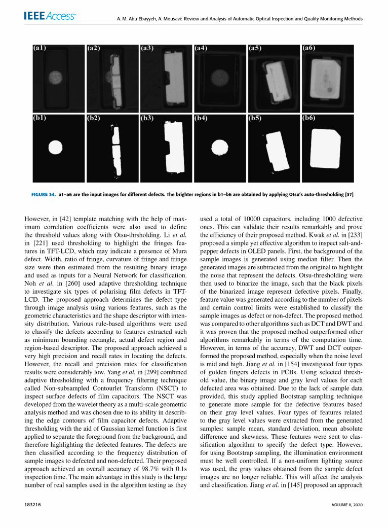
A. M. Abu Ebayyeh, A. Mousavi: Review and Analysis of Automatic Optical Inspection and Quality Monitoring Methods
FIGURE 34. a1–a6 are the input images for different defects. The brighter regions in b1–b6 are obtained by applying Otsu’s auto-thresholding [37]
However, in [42] template matching with the help of max-imum correlation coefficients were also used to definethe threshold values along with Otsu-thrsholding. Li et al.in [221] used thresholding to highlight the fringes fea-tures in TFT-LCD, which may indicate a presence of Muradefect. Width, ratio of fringe, curvature of fringe and fringesize were then estimated from the resulting binary imageand used as inputs for a Neural Network for classification.Noh et al. in [260] used adaptive thresholding techniqueto investigate six types of polarising film defects in TFT-LCD. The proposed approach determines the defect typethrough image analysis using various features, such as thegeometric characteristics and the shape descriptor with inten-sity distribution. Various rule-based algorithms were usedto classify the defects according to features extracted suchas minimum bounding rectangle, actual defect region andregion-based descriptor. The proposed approach achieved avery high precision and recall rates in locating the defects.However, the recall and precision rates for classificationresults were considerably low. Yang et al. in [299] combinedadaptive thresholding with a frequency filtering techniquecalled Non-subsampled Contourlet Transform (NSCT) toinspect surface defects of film capacitors. The NSCT wasdeveloped from the wavelet theory as a multi-scale geometricanalysis method and was chosen due to its ability in describ-ing the edge contours of film capacitor defects. Adaptivethresholding with the aid of Gaussian kernel function is firstapplied to separate the foreground from the background, andtherefore highlighting the defected features. The defects arethen classified according to the frequency distribution ofsample images to defected and non-defected. Their proposedapproach achieved an overall accuracy of 98.7% with 0.1sinspection time. The main advantage in this study is the largenumber of real samples used in the algorithm testing as they
used a total of 10000 capacitors, including 1000 defectiveones. This can validate their results remarkably and provethe efficiency of their proposed method. Kwak et al. in [233]proposed a simple yet effective algorithm to inspect salt-and-pepper defects in OLED panels. First, the background of thesample images is generated using median filter. Then thegenerated images are subtracted from the original to highlightthe noise that represent the defects. Otsu-thresholding werethen used to binarize the image, such that the black pixelsof the binarized image represent defective pixels. Finally,feature value was generated according to the number of pixelsand certain control limits were established to classify thesample images as defect or non-defect. The proposed methodwas compared to other algorithms such as DCT andDWT andit was proven that the proposed method outperformed otheralgorithms remarkably in terms of the computation time.However, in terms of the accuracy, DWT and DCT outper-formed the proposed method, especially when the noise levelis mid and high. Jiang et al. in [154] investigated four typesof golden fingers defects in PCBs. Using selected thresh-old value, the binary image and gray level values for eachdefected area was obtained. Due to the lack of sample dataprovided, this study applied Bootstrap sampling techniqueto generate more sample for the defective features basedon their gray level values. Four types of features relatedto the gray level values were extracted from the generatedsamples: sample mean, standard deviation, mean absolutedifference and skewness. These features were sent to clas-sification algorithm to specify the defect type. However,for using Bootstrap sampling, the illumination environmentmust be well controlled. If a non-uniform lighting sourcewas used, the gray values obtained from the sample defectimages are no longer reliable. This will affect the analysisand classification. Jiang et al. in [145] proposed an approach
183216 VOLUME 8, 2020
A. M. Abu Ebayyeh, A. Mousavi: Review and Analysis of Automatic Optical Inspection and Quality Monitoring Methods
based on Gray Relational Theory for IC marking inspec-tion. The basic idea of gray relational analysis is a rankingscheme that ranks the order of the gray relationships amongseveral sub-systems. Several image processing techniqueswere implemented to apply the gray relational theory. Imagerotation was first applied to make sure that IC is in correctposition for character identification. Morphological openingoperations were then applied to remove noise and help in thesegmentation process for the characters. Thresholding werefinally applied to convert the gray image into binary one inorder to reduce the data amount as possible. Six key featureswere extracted using the previous processes: area, perimeter,ferret elongation, diameter, compactness, and moment wereused to identify the type of problem occurred in the markingprocess such as broken and wrong characters. As comparedto traditional methods (i.e Euclidean distance, Camberra dis-tance, Chi-square, and correlation coefficient), there are threeadvantages in the proposed approach: 1) no large amountof data is needed; 2) no specific statistical data distributionis required; and 3) there is no requirement for the indepen-dency of the factors to be considered. Furthermore, theirproposed approach achieved an identification rate of 97.5%.However, their study did not include IC marking recognitionfor multitype, multidirectional, and various angular settings.Also, they did not include trademarks and punctuations inthe IC marking recognition process. Furthermore, their pro-posed approach did not integrate the software and hardwareinto a whole automatic inspection system. Nagarajan et al.in [146] proposed a similar study for IC marking errors suchas illegible characters, missing characters and upside downprinting. For character recognition, four feature extractionmethods were applied: projection profile, moment, zoning(same as segmentation) and contour profile. After extractingthe features using the four methods mentioned, these featuresare sent to neural network for classification according to thethree error types considered. Their approach achieved 100%classification accuracy. However, the proposed approach doesnot detect marking defects accurately when the IC chips areplaced with rotation angles [147]. Furthermore, the featureextraction techniques considered in this study are time con-suming that takes 1.844 – 2.093s for single inspection task.Said et al. in [204] proposed a study to inspect non-wetsolder joints in processor sockets and BGAs. Images in thisstudy were acquired using X-ray optical inspection system.Thresholding and segmentation approaches were done auto-matically to locate the solder joint regionswithminimal effectof illumination noise. This automatic process can be per-formed with the aid of statistical modelling using a mixtureof Gaussian distributions to find the optimal threshold value.The centroids of the solder joints are then located, and amathematical model were then estimated to check the degreeof alignment of each joint’s centroid with respect to jointsin the same directional cluster. A certain threshold was usedto classify the solders as defected and non-defected accord-ing to the degree of alignment. The conducted performanceevaluation and resulting statistics showed that the proposed
algorithm provides a detection rate of 95.8%. Despite ofthis method effectiveness to deal with nonuniform illumi-nation conditions; however, disregard issues of nonuniformbrightness distributions may lead to over-segmentation andunder-segmentation problems [207]. A similar study [205]was also conducted to detect voids in solder balls. Voids aredefined as cavities formed inside a solder ball due to theamount of outgassing flux that gets entrapped in the solderball during reflow. Themain challenge that this study encoun-tered is to make their algorithm able to differentiate betweenvoids and vias as both vias and voids have similar features.Another challenge is to avoid considering void-like shapesthat are in the solder ball region, which may increase the falsealarm rates. As in the previous study the sample images areacquired using X-ray AOI system. Template matching werefirst applied to choose the perfect template candidate that canbe used to identify other solder ball regions. To exclude vias inthe detection, a method for segmenting vias and locating themwere conducted in this study. The voids are then located andlabelled using certain measures and features such gray levelvalue, area, and compactness factor and certain thresholdswere estimated from thesemeasures to perform the classifica-tion process. Finally, to remove further any detected phantomvoids that were not eliminated by the previous operations dueto similarities with the actual voids, a circularity constraintis imposed and is quantified using the compactness factorand the principal axes ratio. However, the proposed methoddid not show a solution if the actual voids in the final checkwere not of circular shape (e.g. irregular or any complexshape) [330]. Another study conducted by Van Veenhuizenin [208] to inspect voids in solder balls as well; however,deep learning model were used for the defect classificationprocess. Lu et al. in [280] constructed an optical inspectionsystem to measure LCD deformations for smartphones andto locate the position with maximum deformation. The sys-tem consisted of CCD, mirror adjusted with certain degreeand precision plate filled with equally sized holes. If therea deformation exists, the image acquired of the holes viathe inclined mirror will look irregular. Otherwise, if there isno deformation the holes will appear intact. Morphologicaloperation with the aid of thresholding were used to removethe holes along the image edge and to repair the shape ofthe other holes via dilation. A certain threshold was defined,such that if the sizes of the deformed holes are larger thanthe threshold then the LCD is considered deformed. However,there was no discussion about the accuracy of their proposedalgorithm. Jiang et al. in [158] proposed simple image pro-cessing techniques based on thresholding, segmentation, andmorphological operations to detect three types of solder jointdefects. First, to reduce the complexity of feature extractionanalysis, the background is removed using simple thresh-olding to separate the solder joints from the background.Segmentation and dilation operations were then performedin order to highlight the solder joint regions. Two sets offeatures were selected for the determination of normal ordefect solder joints: nine binary image-based features and
VOLUME 8, 2020 183217

A. M. Abu Ebayyeh, A. Mousavi: Review and Analysis of Automatic Optical Inspection and Quality Monitoring Methods
seven gray value-based features. Pareto chart and box plotsfor these features were then examined for selecting the bestfeatures that could discriminate between the normal defecttypes. Finally, rule-based classification was applied usingcertain rule and thresholds to classify the defects according tothe type. Many advantages have been observed in their studysuch as their methodology did not require special lighting orspecial equipment to capture the PCB image. Furthermore,their approach of background removing reduced the compu-tational time for feature extraction. Nakagaki et al. in [127]proposed a system for recognising circuit patterns and defectseverity of semiconductor wafers using thresholding and seg-mentation techniques. The images were collected using SEMand different patterns were observed such as protruding, holeand flat patterns. Hole and flat patterns were identified usingthresholding techniques by calculating the average of pixelsin the binary image resulted. The algorithm for identifyingprotruding patterns were selected according to the densityof the pattern. Thresholding were used again for identifyingdense protruding patterns, while segmentation with the aid ofbinarization and edge detection were used to identify sparseprotruding patterns. The study also classified the defects ofthe circuits in wafers according to the severity of the defectinto killer and non-killer defects. However, the algorithm ofthe classification was not explained. The accuracy for the pat-tern recognition in this study was 98.8%, while the accuracyfor defect severity evaluation was 95.6%. In a similar studyconducted by the same authors in [126], template matchingtechnique were used to analyse the defects. However, thisstudy resulted in minor improvement of accuracy as the accu-racy recorded was 98.9%.
b: REGION EXTRACTIONConnected Component algorithm is a commonly used regionextraction technique which regard each pixel as a node in agraph. Connected Component Labelling (CCL) can be usedafter this step in defect inspection tasks to label the regionsfound (e.g. defective regions) into certain classes. Chang et al.in [44] applied CCL algorithm to identify the number of LEDdies from the binary image map. The algorithm were appliedafter segmenting the die region pixels as 1s and non-dieregion as 0s in a binary image that have the same size asthe original image using Hopfield neural network (HNN).The CCL algorithm examine each die region pixel to giveit a label and compare this pixel to neighbor pixel so thatall neighbor die region pixels are considered as one die.This procedure is repeated until all the dies are recognized.Ooi et al. in [61] proposed a comprehensive data-mining pro-cess using a Segmentation, Detection, and Cluster-Extraction(SDC) algorithm to extract common defective wafer pat-terns from the raw production test data. The proposed SDCalgorithm has been developed to extract meaningful clus-ter features from a database of manufacturing test resultsaccurately and automatically. It can be implemented eitherin an online or offline mode. CCL algorithm were used tosimply pairing adjacent 1s (that represent defective dies) and
0s (that represent normal dies) in a binary image. Finally,morphological operations were used to remove the noisyparts. This study has achieved a 90% accuracy rates in detec-tion. Furthermore, SDC algorithm have helped in reducingthe false alarm rates by more than 90% when compared tousing segmentation algorithm alone. A similar study wasalso conducted by Xie et al. in [96], where four defectpatterns of WMs were generated by connecting-componentsand morphological operation approaches. Wijesinghe et al.in [230] considered similar approach; however, in inspectingliquid resin defects in LCDs. The acquired images from theOCT are binarized and pixels were classified as defectiveand non-defective according to certain threshold related tothe intensity. Next, CCL technique were used to define theboundary of the defective regions and non-defective regionsby grouping each pixel’s class together. This technique isrepeated until all regions are classified. Using this approachdoes not only evaluates the particular defective location; how-ever, it defines the magnitude of each defect, and the numberof defects in a unit sample.
Sindagi and Srivastava in [281] used two feature extractionapproaches to highlight micro and macro defective featuresof OLED panels and generate feature vector to be used asan input for the classifier. Due to its important advantagesof computational efficiency and good texture discriminativeproperty, a modified version of Local binary patterns (LBP)was considered as one of the approaches for feature extrac-tion. In LBP algorithm, a 3 × 3 operator is used to compareeach central pixel with its eight neighbor pixels to generate abinary code that can be converted to a decimal value. Theneighbors which have smaller pixel value than the centralpixel are set to logic 0, otherwise they will be set to logic 1.Then the generated binary code resulted from the neighborpixel value can replace the central pixel value. In the modifiedversion of LBP, a uniformity measure is defined which isthe number of transitions between 0’s and 1’s in the LBPcode. Patterns having uniformity measure below a certainthreshold are labelled as uniform. During the evaluation ofthis method, it was observed that it performed well on macrodefects like pit and film tear but failed to be effective onmicro defects like scratch and spot. Therefore, another fea-ture extraction technique called local Inlier–Outlier Ratioswere integrated with LBP to be able to detect micro defects.Lin et al. in [231] considered segmentation-based methodcalled wrapping to locate the bright spots defected features inlight guide plate of LCD panel. At the beginning, the entireimage was scanned to find a bright spot. The system thenscans along the upper part to the edge of the spot. The distancebetween the lower and upper edges is calculated and a centerpoint were estimated by dividing the distance by two. Thecenter point measured represents the center of the bright spot.A circle wrapping method is proposed in this case wherethe scanning sequence follows a counter-clockwise rotationfrom one corner to the opposite corner until all of the brightspots have been marked. Certain measurements were thenapplied to assess the quality of the bright spots. However,
183218 VOLUME 8, 2020
A. M. Abu Ebayyeh, A. Mousavi: Review and Analysis of Automatic Optical Inspection and Quality Monitoring Methods
the classification procedure was not explicit. Furthermore,there was no discussion for the computation time required noof the accuracy achieved. Kubota et al. in [120] used RegionGrowing to extract the shape feature of the micropipe waferdefect. Their algorithm procedure starts by extracting pointsof local minimum within a square region of pixels centredat the pixel of question called neighborhood region. If thelocal minimum point value is within predefined range, thenthis point belongs to the specified region. Furthermore, theyextracted the surface curvature features of the defected. Thenthey created a feature vector out of the extracted features andfed it to a neural network for classification. Hsieh and Chenin [63] used multiple feature extraction approaches basedon sub-region analysis for defining the possible defectivepoint of semiconductor wafers. Then they applied MinimumRectangle Area approach to combine the defective points intoclusters. However, they did not mention how to specify thenumber of clusters or and how to use clustering features toseparate various types of defect patterns [67]. Hui and Pangin [177] proposed a study to detect solder paste defects by firstconstructing 3D profile to represent the solder paste block.Segmentation technique were used to divide the block intofour edges and surface top area. The overall solder paste blockis also considered to be another region. A global classifierwas used to assess the quality of the overall block regionand declare if there is a defect or not. Two features wereused to feed this classifier which are volume and aspect ratio.However, a solder paste block can still be defective if itpasses the global classifier. This is because a deformed solderpaste block can have the same volume and aspect ratio as thenormal one. Therefore, additional five local classifier wereestablished corresponding to the five regions segmented.Same features were considered for the four edges which arecontour lines standard deviation and area of the edge, wherethese features are fed to four classifiers. While top surfaceheight standard deviation and area of the top surface werechosen as features for the top surface region classifier. Finally,AND logic operation was implemented between the outputof local classifiers and global classifier, such that if a defectis detected in one of them at least this means that the finalresult will show a defect is detected. Despite of achieving a100% detection rate in this study, they did not mention thenature of the classifiers chosen. Furthermore, since a totalof six classifiers were chosen in this study, it was importantto mention the computational time needed for classification.Liao et al. in [95] proposed morphology-based similarityapproach to generate simple and complex wafer samplepatterns with certain degrees of similarity, as compared tothe objective target WMs. Several morphological operationswere used in this process including dilation, erosion, open-ing, closing, position shift, density change and rotation withvariations. The generated data were then sent to classifier tospecify the type of the patterned defect. Lin and Lue in [201]proposed a fast positioning and inspections system for BGAs.Edge detection and thresholding techniques were first appliedto find the boundary regions of the pads and holes, then using
the least-square circle approach the centers of the holes andpads are found. The alignment shift is then tested by usingfour sample images, where the centers of holes and pads forthese sample images are compared together. Certain thresh-olds were used to decide if the variation resulting from thecomparison process are accepted or not. Unfortunately, thisstudy did not provide any information about the efficiency ofthe proposed method in terms of the recognition accuracy andcomputational time. Deng et al. in [225] investigated trans-parent aesthetic defects of polymeric polarizers by simulatingthem using a microscale plano-convex lens. They employedgray morphology (dilation and erosion) approach to identifythe investigated defects and extract the features of them. Thefeatures extracted were related to location, shape and size ofthe defects. Despite of having an efficient detection systemwith relatively low time of detection 1.6s and considering thefact that detection of the simulated defects were consistentwith the experimental results. However, this study did notconsider an algorithm for defect classification. Furthermore,they mentioned that irregular defects can be simulated byusing irregular shaped lenses; however, they did not ver-ify their claim experimentally. Finally, they did not showthe necessity of using such a simulated technique. Authorsin [226], [229], conducted similar approaches; however, theyconsidered extremely slight transparent aesthetic defects.
c: EDGE DETECTIONOne of the used segmentation techniques to extract used inmachine vision applications is edge detection. This techniqueis very useful in applications that requires locating a feature,alignment or for gauge inspection and measurements. As thename says, edge detection is used to find boundaries in theimage and sharp edges, this can be performed by locatingthe discontinuities in pixel intensities in the image using sev-eral filters and operators such as Prewitt, Canny, and Sobel.Pixels that are found on the boundary using this techniqueare called edge pixels. An edge pixel can be described usingtwo parameters; edge strength (also called edge contrast)which defines the minimum difference in the grayscale valuebetween the edge and background, and edge direction, whichcan be defined by the angle of the edge direction [309].Chang et al. in [288] proposed simple image processingalgorithm that relies on thresholding and edge detection toclassify touch panel defects. The distance measured betweenthe edges of the defects were considered as the criteria fordeciding the defect type. For instance, if the measured widthand length of the defect ranges from 7µm to 21µm and 1 mmto 10 mm respectively, the defect is classified as crack defect.The accuracy of the proposed algorithm ranged from 94-99%depends on the defect type. However, the inspection time ofthe algorithm was relatively long due to the high-resolutionimages considered. In the two studies conducted byChao and Tsai in [262], [266], an improved anisotropicdiffusion technique was used to highlight defects in lowcontrast surface images of glass substrates and back-light module in LCD respectively. Anisotropic diffusion
VOLUME 8, 2020 183219
A. M. Abu Ebayyeh, A. Mousavi: Review and Analysis of Automatic Optical Inspection and Quality Monitoring Methods
(also called Perona–Malik diffusion) is an image process-ing technique that can reduce the noise in the image withmaintaining important features of it such as lines andedges [331]. This quality of the technique makes it reliableto deal with low contrast images to highlight the defects.In [262], an adaptive smoothing process were integratedwith the original technique to further enhance the detectionprocess of defects in glass substrates based on the variationof gradient in the image and by adjusting certain parametervalues. For defect classification, the lower and upper limit forintensity variations were estimated by calculating the meanand standard deviation of the gray values of the image. If thegray level of a pixel falls within the control limits, the pixelis classified as a faultless point. Otherwise, it is classifiedas a defective one. The computation time of this study wereestimated to be 0.3 s; however, in [266] they referred tosame study time as 0.16s. Therefore, the real time was notcompletely clear as there is a contradiction between bothinformation. In [266], the original technique were furtherimproved by integrating PSO to automatically determine thebest parameter values of the anisotropic diffusion functioninstead of manually as in the previous study. This study wasconducted to detect low contrast backlight module defectsin LCD. The classification criteria of the defects in this studywas the same as the previous one. The computation timewere improved to be 0.06 s with lower number of iterationscompared with the previous study. Despite of the algorithm’sability to highlight low contrast defects, this algorithm onlyperforms well with non-textured surfaces, which means it isnot suitable to detect all kind of defects in LCD parts.
d: HOUGH TRANSFORMHough transform were also one of the techniques used forfeature extraction and defect detection applications, due tothe ability to detect various shapes (e.g. linear, circular andelliptic shapes), given a parameterized description of theshape. Edge detection operations are used as preprocessingprocedures before applying Hough transform. This techniqueis very suitable for detecting wafer defects patterns in WBMas they tend to follow a specific pattern. Since WBM areconsidered binary images, Hough transform transforms thebinary image into a parameter space and tries to detect theparameterized pattern through a voting process in which eachpoint votes for all the possible patterns passing through it.Patterns with a higher number of votes indicate a higher prob-ability of the occurrence of this pattern on the map. As longas a parameterized model can be established for the spatialpattern, this method can be adopted [59]. White et al. in [74]used Hough transform based on linear parameterization todetect defective dies patters on WBM. The patters detectedin this study were of linear shapes such as scratches and edgepatterns. Themain advantage of this study is its simplicity andthe ability of being fully automated. However, the study wasnot useful in detecting commonly defective WBM patternssuch as ring patterns. Zhou et al. in [82] presented a controlchart technique to detect line and circular patterns through
statistical evaluation using Hough transform. This statisticalevaluation calculates the number of votes for the line andcircular defect maps. When the number of votes is largerthan the control limit, an alarm is raised indicating that apattern is detected. However, this method cannot distinguishspecific definite cluster patterns such as blob, bull’s eye, edge,and ring. Chang et al. in [59] applied Hough transform todetect WM defect patterns and were able to overcome thelimitations in previous studies by detecting all the patters thatwere missed by them.
Despite of Hough transform’s ability of detecting variousdefect patterns, this technique is considered insensitive togaps (missing pixels), which make it difficult to detect ran-dom or mixed pattern defects in WMs since it may groupthem as one pattern instead of multiple ones [74]. Houghtransforms performs poorly when it comes to low contrastimages, this may not be a problem in WMs since they aregenerated using circuit probe techniques. However, it maybecome serious problem in other cases that utilize illumi-nation to highlight small defects such as Mura defects inLCDs. Furthermore, Hough transform is considered costlyin terms of computational time [248]. Li and Tsai in [248]proposed a revised version of Hough transform to highlightdefected Mura features in LCD such as spot, line, and regionMura. This revised version can detect low-contrast defectin 1D gray level image with uneven illumination. Unlikeconventional Hough transform that are insensitive to gapsand needs sufficient number of points to detect line defect,this method can accommodate distance tolerance. Any pointwith the distance to the line falls within the tolerance will beaccumulated as a function of the distance to the line sought.This approach allows the nonstationary points contribute tothe accumulator in the voting processing. Despite of theproposed method’s ability to outperform the conventionalone; however, it is only capable of detecting nonstationarystraight-line and cannot consider nonstationary curved pro-files and nonstationary linear/curved surfaces. Chang et al.in [297] used Hough Transform as a preprocessing approachto transform the circular shape of camera lens’ into a linearshape before inspecting the defects. After the transformationfrom the polar coordinate into Cartesian coordinates, seg-mentation and morphological operations were conducted tosegment the defects. Five features were extracted from theprevious process which are the area of defective regions,ratio of the width and height of defective regions, mean ofthe gradient of defective regions and variance of the gra-dient of defective regions. Where the feature vector con-taining these five features is sent to classifier algorithm fordeciding the defect type. Jin et al. in [207] introduced areference-free path walking method to recognize the BGAcomponent locations and diagnose solder ball defects suchas oversize ball, undersize, ball bridging, misshapen ball,missing ball, and ball offset. Solder balls were first segmentedusing adaptive thresholding and median-based Otsu methods,which determine local thresholds for individual cells, to over-come nonuniform brightness. Then path-walking method
183220 VOLUME 8, 2020
A. M. Abu Ebayyeh, A. Mousavi: Review and Analysis of Automatic Optical Inspection and Quality Monitoring Methods
(which is a modified Hough-transform approach) to locatethe orientation and position of the balls and extract thedefective features. Three features are then extracted usingthese steps which are solder ball area, center of gravity andcompactness. Certain rules were then set according to theextracted features to classify the defects. The main advan-tage in this method that it does not need a reference imagewhich make it more practical in real inspection applica-tion. Similar study was also conducted by the same authorsin [157] to inspect solder balls defects using course andfine positioning technique. Unlike the previous study, thismethod is model-based in which edge detection filter anda circle fitting methods are employed to obtain the coarseand fine locations of solder balls, respectively. The approx-imate location of the component is then estimated using ageometrical method and the fine location is calculated bysolving a least-squares problem. Finally, a pair of overlap-ping ratios were used to classify solder ball defects basedon their quality and to inspect the accuracy of alignment.Compared with the previous study, this method consumedless computational time for same amount of BGA inspected.However, the accuracy measures in this study was lower thanthe previous one. A third similar study was conducted by thesame authors again to investigate the same defects in [136].Segmentation and adaptive thresholding were applied in thisstudy as well to locate the solder balls; however, line-based-clustering approach were added to coarsely determine theBGA orientation and to classify the solder balls accordingto their row and column locations in the BGA array for thefeature extraction process. Four features are then extractedafter performing the previous steps which are ball area,ball centroid bias, roundness, and ball arrangement matrix.Finally, certain rules are considered according to the featurevalues in order to classify the defect types. The performedapproach outperformed the previous two methods with 100%detection accuracy. However, the computational time con-sumptionwas theworst among them all with 200ms to inspect500 solder balls. Kuo et al. in [259] proposed an opticalinspection approach to highlight various kind of defects inpolarising films of LCDs such as dust, foreign object, scarsof hit, bubble and scratch defects. Various image processingand feature extraction techniques were used for this purpose.First, downsampling compression were performed to reducethe size of the inspected images, then Laplace operator wereused to detect the edges of the defects. Thresholding andHough transform were finally used to differentiate the spotdefects, like dust, foreign objects, scars of hit and air bubblesin the production process from the line defects, like scratches.This study was able to speed up the inspection time byusing downsampling technique as they were able to reducethe image size by 64 times. Furthermore, they achieved adifferentiation rate up to 98% in sorting spot defects fromline defects. However, this study did not propose a classi-fication technique to classify each type of the investigateddefects
3) TEMPLATE MATCHINGTemplate matching is considered one of the simplest andearliest pattern recognition techniques [332]. In AOI appli-cations, template matching algorithm works by first iden-tifying a reference template which usually represent thenon-defected case (also known as golden template) that canbe used for comparison. The selected template can be com-pared to the target samples using various kind of correlationfunctions. Template matching is preferable in investigatingsystematic defects that have common patterns. The reasonbehind that is the defect is always compared with a referencetemplate so if the defect occurs is not systematic, the compar-ison with the reference template will fail and high false alarmrates will occur. Template matching techniques can be usedin most application; however, it is not preferable in inspectingWMdefects, since most of these defects are of mixed patterns(systematic and random).
Normalized cross-correlation (NCC) function is one ofthe most commonly used template matching functions,it involves sliding the sub-image over the larger image pixelby pixel and calculating normalized correlation to estimatethe degree of similarity between the sub-image and thelarge image regions [137]. It has been proven to greatlyreduce the data storage and also reduces the sensitivity toacquired images when compared with traditional image sub-traction [333]. Zhong et al. in [48] proposed blob analy-sation and template matching approach based on NCC toinspect polycrystalline and fragmentary defects on LEDchips. Regional image segmentation was first performedto locate the blob defect features and exclude them. NCCapproach were also used to locate LED chips at pixel accu-racy. A certain threshold was used to classify the abnor-mal LEDs from the normal ones. The study showed goodaccuracy in detecting normal chips with zero false alarmrate. However, a false alarm rate is presented in detectingdefective chips because of the NCC threshold value selected.Despite of NCC simplicity, this method is time-consumingsince it is based on 2D summation and multiplication oper-ations to compute the correlation, and is often combinedwith the image pyramid method to compress image size toalleviate the computation load of the correlation coefficientmethod [45], [179]. Furthermore, this method is very sen-sitive to illumination variations and image shifts, which canincrease false alarm rates [188]. In order to reduce the timecomplexity of this method, Crispin and Rankov in [179]proposed a modified NCC based template matching approachusing the generalized gray- model template for inspectingcomponent placement errors in PCBs such as missing, mis-aligned or incorrectly rotated components. The gray-modeltemplate can extract a vector of all edge positions of theinspected component. By only searching the image at edgelocations, the number of NCC calculations that are neededto be performed can be significantly reduced. Genetic algo-rithm was also proposed to replace the sliding sub-imageprocess involved in NCC operation. Despite their efforts in
VOLUME 8, 2020 183221

A. M. Abu Ebayyeh, A. Mousavi: Review and Analysis of Automatic Optical Inspection and Quality Monitoring Methods
reducing the computational time of the NCC approach, thismethod did not mention the classification criteria for theinvestigated errors (missing and misaligned component). In asimilar study, multi-template matching algorithm proposedby Wu et al. in [184] that utilizes NCC for component place-ment inspection on PCBs. The searching process has beencarried out by using the proposed accelerated particle swarmoptimization (AS- PSO) method to reduce the computationaltime needed for detection. AS-PSO method were also com-pared to GA for its ability to perform the same function.However, experimental results have shown that AS-PSO wasable to reduce the computational time requiredmore thanGA.The recognition rate achieved in this study reached 100%;however, the testing was performed on resistors only anddid not involve other components. Similar approach was alsoproposed in a similar study conducted by the same authorsin [185] with some modification to the PSO searching algo-rithm. However, the same drawback of the previous studywas also found in this one. Furthermore, the processing timein this study was much higher of that in the previous one.Annaby et al. in [137] suggested an improved normalizedcross-correlation (INCC) algorithm to discover the locationof missing ICs. The suggested algorithm work in 1D insteadof 2D, which reduce the computation time and robust againstnoise. Moreover, subtraction of the local mean in the INCCprovides better robustness than NCC since INCC toleratesuniform brightness variations. Despite their algorithm’s abil-ity of reducing the computational time compared with NCC,their algorithm did not improve the accuracy of the NCCapproach. Wang et al. in [188] have also proposed a modifiedversion of NCC called partial information correlation coef-ficient (PICC) to inspect surface defects such as particles,foreign matters, and distorted components in PCBs, BGAsand ICs. The PICC uses the technique of significant pointsto calculate the correlation coefficient. The PICC algorithmprocedure has to set three variables: the size of the inspectionwindow, the gray level threshold, and the correlation thresh-old. The most important difference between NCC and PICC,is that the PICC firstly uses the gray level threshold to obtainsignificant points in the inspection window and calculate onlythe correlation coefficient of the selected significant pixelpoints. Therefore, the inspection speed as well as the falsealarm rates can be significantly reduced. The second PICCthreshold is the correlation threshold. This value is used todecide whether the image contains a defect. The selectionof the proper correlation threshold is also a key factor todetermine the algorithm is stable. Experimental results haveshown that this method achieved up to 100% detection ratewith only 0.3s, compared with 7s in NCC. However, if thereis a gap in the expected results, users must determine a newset of variables for applying PICC procedure.
Pearson’s correlation coefficient (PCC) is also one of thecorrelation functions used in template matching for com-paring the reference image to the sample images. UnlikeNCC, PCC is considered more robust to variations con-cerning brightness and noise. This method were used by
Timm and Barth in [20] to detect p-electrode defects inLED dies; the study assumed that the template and sam-ple images have the same height and width and they pro-duced a formula based on that assumption with the aidof the mean and standard deviation of the template andsample image. Ibrahim and Al-attas in [156] proposed atemplate matching and wavelet-based approach to inspecttraces defects in PCBs. Reference image was considered asthe perfect template for performing the comparison process.Two-dimensional HAAR wavelet transform was applied onboth reference and sample images to perform the compar-ison on the wavelet domain. To avoid unwanted noise dueto misalignment and uneven binarization, the comparisonbetween the reference and sample images in this study isperformed using subtraction process. The output of the imagesubtraction operation can be one of the following three cases:positive (potential defect), negative (potential defect), or zero(non-defective). The generated positive and negative imagesare binarized and then subjected to a noise elimination pro-cedure. These images are lastly sent to XOR logic opera-tion as a final classification to decide whether the imagesrepresent a defect or not. Many limitations were found inthis study; first, the accuracy and the time requirement fortheir inspection system were not discussed. Secondly, despiteof mentioning fourteen types of defects that their systemcan detect, their classification scheme only classified thesedefects using binary approach (defective and non-defective).Lastly, their proposed system can be applied for small andmedium fabrication scale only, and cannot be implementedfor mass fabrication systems [334]. Cho and Park in [180]proposed a similar method; however, for inspection of com-ponent defects such as missing component, wrong compo-nent, rotation, and tombstone. As in the previous study thewavelet transform for the reference and sample images werefirst performed. For the matching process between the ref-erence template and sample image, the mean absolute dif-ference and the mean square difference (MSE) are used tomodify each pixel and the whole image matching is per-formed. To reduce the calculation time in matching, the areaof objects was segmented from the overall area of inputimage. The segmentation step identifies the object area fromthe compressed image. Their approach was compared to DCTand results showed that their method outperformed DCT. Themain advantage of this study is its ability of reducing thememory size, as they have reported that they used 7% onlyof the original image for the inspection process. This couldbe also considered a disadvantage as important features maybe lost by reducing the size of the image to this scale. Theirinspection accuracy was highest in detecting missing com-ponent defects with a 96.7%. However, experimental resultshave shown that variation of brightness and texture highlyaffect the accuracy as well as the time consumption of thealgorithm. Unfortunately, the proposed method did not offera solution to mitigate these effects. Tsai and Huang in [200]proposed a method, that can be used to investigate PCB andIC dies defects, based on the comparison of the whole Fourier
183222 VOLUME 8, 2020

A. M. Abu Ebayyeh, A. Mousavi: Review and Analysis of Automatic Optical Inspection and Quality Monitoring Methods
transformed image between the template and the sampleinspected images. It retains only the suspicious frequencycomponents in the Fourier domain of the test image and dis-cards the common frequency components. After the anoma-lies are detected and the background has been removed,the inverse Fourier transform is then applied to restore thesample image. A simple statistical control limit is finally usedas the adaptive threshold to segment the local defect for clas-sification purposes. Unlike conventional template matchingapproaches, this method is considered invariant to translationand illumination variations in the sample images. Moreover,the proposed approach can detect subtle defects as smallas 1-pixel wide. Liu et al. in [114], [115] proposed similarapproach to detect IC wafer defects. In their studies theyused 2D and 1D DWT respectively to extract a standardtemplate image form three defected images using comparisonand subtraction approaches. In [115], they showed that theaccuracy of detection does not differ between 1D and 2DWT,while the computational time in 1D DWT is less than 2D.The advantage of this method is its robustness to illumination.However, the accuracy measures for these methods were notmentioned in both studies. Rau and Wu in [192] proposedtemplate matching approach to inspect inner layer defectsof PCB board. First, a golden template of PCB board wasdesigned using CAD tools for comparison process. Beforethe comparison takes place, the sample images were normal-ized by applying geometric transformations such as rotation,scaling and shifting. Then image subtraction is applied tocompare between sample images and the golden template.The result of the subtraction process will result in eithermissing pixels or excess pixels. Missing pixels correspondsto defects such as pens, mouse bites, pinholes and missingconductors while excess pixels correspond to shorts, spurs,excess copper, and missing holes defects. In order to segmentthese defects, a 4-connectivity logic operation is used todetermine the outer boundary of objects in a binary image.Finally, classification algorithm called boundary state transi-tion were proposed to classify the defects according to the8 investigated defects. The proposed method is consideredsimple to implement and computationally inexpensive; how-ever, image subtraction algorithms are sensitive to variationsin illumination, lighting, color and complex transformations,which may affect the detection accuracy. To investigate tracesand cosmetic defects in PCBs, Liao et al. in [194] usedtemplate matching approach based on Hausdorff-distance.The sample inspected images are compared with a referencetemplate image, that is generated from the compilation ofseveral good PCBs, for aligning them with each other. Thealignment process can also help in locating the defects andextracting their features. Several techniques were used inthe alignment such as sobel edge detector and geometrictransformation as well as finding the minimal Hausdorff-distance. It has been found that traces defects of PCB followspecific patterns, therefore the features of these types ofdefects are directly sent to the classifier for performing theclassification. However, cosmetic defects possess irregular
appearance, therefore for this type of defects color featuresare also considered in the classification process. Comparedwith other comparison approaches that are based on XORoperation and logical rules, the proposed approach requiredless time for extracting the features. Chang et al. in [193]proposed two-phase approach to inspect PCB traces defects.The first stage starts by storing sample images to form con-cept space. Segmentation and morphological operations toextract the features of the defect. The resulting images arethen compared with template image that represent the idealPCB image using rule-based method and XOR operation.The second phase, which is called case based reasoning, is asystem that can be created with a small or limited amountof experience and then developed incrementally by addingmore cases to the concept space as they become available.The hybrid approach can avoid the main disadvantage of hightime consumption in template matching algorithm. Wu et al.in [162] proposed template matching approach to investi-gate solder bump defects. To do that a reference templateimage was generated that represents the perfect non-defectedcase. Using several image processing and feature extrac-tion techniques such as thresholding, morphological opera-tions, segmentation, and geometric calibration, four featureswere extracted from template and sample images. Thesefour features are area of solder bump, the number of edgepixel, the deviation from center, and the deformation ratio.A comparison process were performed for the features ofthe template image to that of the sample images. Given aset of lower and upper limits rule, the defects are classifiedaccording to the matching score between the template andsample images. The proposed method achieved a high recog-nition rate of 97.96% with a low false alarm rate of 2.61%.However, in order to achieve these good results large numberof samples were required (10600 samples), which will sig-nificantly increase the computational time. Hassanin et al. in[181] investigated more general faults on PCB boards such asmissing letters, missing component and flux cutting. SpeededUp Robust Feature Extraction (SURF), segmentation andtemplate matching approaches were used to highlight thedefects. However, their approach is very time consumingwitha total time of 6.5211s for single image inspection, whichmay prevent their study to be implemented in inline opticalinspection system. Owing to its robustness and its abilityof providing distinctive descriptors to the size and rotationtransform, Yuk et al. in [195] have also proposed SURF algo-rithm for extracting PCB surface defects such as scratchesand improper etching. The features extracted represent infor-mation such as the size, angles, coordinates, and color of thedefected region by digitalising the input image into a featurevector that contains the previous information. Hessian matrixis used in the algorithm for detecting interest points, whichrepresent the characteristics of the image and include usefulinformation for identification, including corner points. Haarwavelet transform is also integrated with SURF to furtherincrease the robustness and decrease the computational time.The extracted features are then sent to a classifier to decide
VOLUME 8, 2020 183223

A. M. Abu Ebayyeh, A. Mousavi: Review and Analysis of Automatic Optical Inspection and Quality Monitoring Methods
the source of the defect. Lin et al. in [274] suggested amodified pattern matching method to inspect andmeasure themovement of anisotropic conductive particles. The study usedpattern setup and analysis to add a matrix of miscellaneousgray scale to an adaptive one and run a miscellaneous algo-rithm on part of the pattern block to improve the executiveefficacy of the system. Adaptive feature weight matrix isalso introduced to reduce error match. This research wasable to identify defective patterns with relatively short timecompared with conventional pattern matching techniques.However, the number of samples used for testing and thefact that no classification algorithm was considered are majordrawbacks in the study. Ye et al. in [176] inspected the ICsolder joint component based on an algorithm they call it‘‘Adaptive template method’’. The algorithm start workingby a constructing a dictionary of qualified IC solder images.Certain coefficient can be calculated using the dictionaryscheme. These coefficients can be used to construct adaptivetemplate assuming that an unqualified image is consideredas a combination of qualified template and noise. Here thenoise is considered to be the defect. Hue channel was usedas the feature to be considered in calculating the differencebetween the sample images and the templates. Since relyingon the difference only may result in a misleading data, eachpixel has a specific weight that depends on the location ofthe pixels where most likely a defect will occur. Variousexperiments using several number of penalization functionswere used to evaluate the quality of the inspection. For clas-sification, a threshold R is defined based on the hue chan-nel difference between the template and sample image fromthe dictionary, to identify whether a pixel in the differenceimage is a potential solder joint defect pixel or not. However,their approach classified solder joint defects as qualified andunqualified without mentioning the defect type. Cai et al.in [173] studied IC solder joints defects by comparing a goodsolder template models (qualified) to other sample images(qualified and unqualified) in a video frame. The inspectionalgorithm used in this paper is Visual Background extractionalgorithm (ViBe), which is originally developed for movingobject detection. This method has the advantage of overcom-ing the feature extraction and selection process, determiningof specific threshold for image analysis and debugging ofnew products. Six templates were used instead of 20 as inthe original algorithm usage in object detection to decreasethe complexity. These templates were considered accordingto the hue-channel values. Despite of achieving a 99% inspec-tion accuracy when using large number of training samples,this method does not explore prior knowledge and consideredcomplex to use. Moreover, their proposed approach assessesthe overall quality of the solder joint without specifying thecause of defect. Wang et al. in [189] proposed template-matching-based approach to evaluate drilling quality ofPCB holes. Their method is capable in detecting three typesof PCB defects: missing holes, incorrectly located holes, andexcessive holes. After applying preprocessing, rotation, andscaling operations on the sample images to match then with
the reference templates, several features are calculated andextracted such as the centers, radius, roundness, and otherdiameters of the holes. The ratio and angle of rotation arecalculated between the testing and the reference images, thenthey were modified until they became in the same direc-tion and at the same angle. In this paper, the centers of theholes are in the most upper left and most upper right as twodatum points for both testing and standard images. Templatematching can be then applied between reference and testingimages by using three key performance indicators as thresh-olds which are average and variance for center holes, centercompensation, and unit circle scale. Their approach canbe effectively applied for high resolutions of 5µm andabove. However, many limitations have been observed in thisstudy. First, their approach is considered lengthy and com-putationally expensive as the total inspection time requires2.5 seconds. Second, the ratio between reference templatesand testing images is manually calculated, which makes theirapproach not fully automated. Finally, by using the mostupper left and right points as datum points, it would causeerrors because if one or two of them are missing the resultwill fail. Hsu and Shen in [147] proposed an approach basedon template matching to inspect IC marking. Their proposedmethod starts by first detecting the angle of the chip and thenusing the sum of absolute difference similarity measure tomatch the template image and sample image. To reduce thescanning time in the inspection process, the detection algo-rithm was implemented on a multi-core embedded processor.In addition to that, the operations of the algorithm wereperformed in parallel using Single Instruction Multiple Datainstructions for Arm processors known as NEON. The timeneeded for their algorithm to distinguish good from bad ICsreached 31ms. Their proposed approach overcame some lim-itations that were found in similar previous studies in [145],[146] by detecting marking defects accurately when the ICchips are placed with rotation angles, reduce the computa-tional time and integrating the software and hardware into awhole automatic inspection system. However, their methodclassified the IC marking as good and bad, without highlight-ing the cause of the error. Lee et al. in [279] used multiplefeature extraction methods to highlight TFT-LCD pad areadefects. The proposed method utilizes an adaptive discreteFourier transform (DFT)with the aid of a golden template thatis transformed using DFT as well to precisely remove widerrange of pattern frequencies. The main advantage of thismethod that it works well on an image having both impedancematching and fan-out areas as these areas either have a chang-ing pattern period or non-repeating components. In the threestudies conducted by Acciani et al. in [143], [165], [166],different feature extraction techniques were used to classifyfive types of solder joint defects. They first used templatematching approach to highlight the extract the ROI in sampleimages, which represent the solder joint and IC area forinspection. Ten geometric and eight wavelet features wereextracted from the inspected area andwere combined togetherto construct one feature vector. The obtained feature vector
183224 VOLUME 8, 2020
A. M. Abu Ebayyeh, A. Mousavi: Review and Analysis of Automatic Optical Inspection and Quality Monitoring Methods
was then used as an input for a classification algorithm inorder to classify the defects according to the five types consid-ered. A similar approach were used in a study conducted bythe same authors in [167]; however, in this study less featureswere considered for the defect detection task. Three instead often geometric features that represent area of the solder fillet,mean gray level of the image and barycenter position of thesolder area were obtained in this study using thresholdingand segmentation techniques. Furthermore, wavelet featureswere not considered here, which reduce the computationaltime and allows the feature extraction process to be performedautomatically without the need of a human expert.
Template matching is still facing some limitations thatmakes it difficult to use and increase false alarm rates, theselimitations include requirement of the reference and testimages to be exactly aligned and high influence of noiseand illumination settings. One of the major limitations oftemplate-matching for inspection is that an enormous num-ber of templates must often be used, and this makes theprocedure computationally expensive [306]. To overcomethese limitations, Kim and Yoo in [117] proposed FeaturePoint Matching approach to inspect defects in wafer images.This method starts by studying the features that may differdefective image than the reference images such as contour,edges, and corner points. Therefore, a feature point has aspecial property distinguishable from its neighbor points.In this method the comparison is between features insteadof pixel-by-pixel comparison as in conventional templatematching approaches. In this study corner points were used asfeature points for comparison, as it has been found that waferimages with defects results in additional corner points anddifferent gradient values compared to those in the referenceimages. It has been proven the proposed method outper-formed other template matching methods such as subtraction,NP-subtraction, NCC and Eigenvalue. Furthermore, it is lesssensitive to alignment and noise. However, this method wasnot able to locate defects and the processing time has to befurther improved in case online testing is required. Xie et al.in [110], [112] proposed self-referencing method, in whichthe dataset of images used for defect detection are also usedto create reference image that is used in template matchingmethod. Their algorithm has a learning ability of refining thereference image in case a better match was found. This abilitydoes not require repeating the comparison steps between thereference and sample images which reduce the computa-tional time of the process. Furthermore, their algorithm isnot affected by image alignment and uneven illumination.Despite of all mentioned, their study did not propose a cri-terion for defect classification. Jian et al. in [284] overcamecommon limitations in template matching techniques suchas misalignment, and surrounding illumination variations,by proposing contour-based registration (CR) method to gen-erate the template image. In this technique the contour isconsidered main feature for alignment such that in the caseof rotation and translation, the contour geometry remainsunchanged. This algorithm was used to inspect mobile screen
glass defects. A subtraction and grayscale projection werethen conducted on acquired images and template to extractdefect. Using certain threshold, an internal classification pro-cedure was performed to binary classify the sample imagesinto defected and non-defected samples. Finally, an improvedFuzzy c-means clustering (IFCM) technique were proposedto segment defects with fuzzy boundary contours. Despiteof the good sensitivity and specificity results achieved inthis study, the approach considered did not include finalclassification process to classify the defects according to theirtype. Furthermore, the inspection time of 1.6601s is con-sidered relatively long for on-line inspection environment.Also according to [285], it is insufficient for image distortionrectifying to consider only rotations and shifts, and thus theextraction after subtraction is not accurate. In a similar studyconducted by the same authors in [283], an AOI systemwere proposed to inspect mobile screen glass defects suchas scratch, pit, dirt, and edge breakage. In order to avoidthe problem of higher dimensionality features that exists incommon feature extraction techniques, this study proposed atechnique based on multifractal spectrum for feature extrac-tion. Using this technique, only two features can be extractednamed multifractal spectral width and spectrum subtraction,which are considered for classifying the defect type usingclassification algorithm. Liang et al. in [287] proposed AOIsystem to detect touch panel defects. In their approach, theyfirst calculated the gray-values of the images and consid-ered them as feature values. Then they established a dictio-nary of defect-free features; however, since these featurescan be redundant, sparsely reconstruction were proposed tochoose the optimum set of features. Orthogonal matchingpursuit (OMP) were then used to sparsely represent the test-ing images based on the dictionary. Finally, sparsity ratio ofthe sparse representation coefficients (between testing imageand template) is estimated to determine whether the testingimage is defective or not with the aid of certain thresh-old. Experimental results showed that under various illu-mination conditions, the proposed approach can efficientlyand quickly detect the touch screen defects for low res-olution images and different defect types. However, theirapproach used binary classification (defected, non-defected)for inspection without specifying the defect type. Further-more, their approach is considered computationally expen-sive since their method is highly iterative. Tsai and Hsiehin [29] proposed a template-matching-based algorithm thatcan be used for detecting both PCB and LCD polarizer filmdefects. To solve the alignment problems encountered intemplate matching approaches, this study used fast imagealignment method called the expectation–maximization(E–M) technique. This technique starts with edge detection toextract edge points in the image. The E-step of the E–M pro-cedure finds mutual edge points in both compared referencetemplate and sample inspected image by assigning weightsto individual edge points. The mutual edge points give largerweights, while the foreign edge points in two images havesmaller weights. The M-step then calculates the geometric
VOLUME 8, 2020 183225
A. M. Abu Ebayyeh, A. Mousavi: Review and Analysis of Automatic Optical Inspection and Quality Monitoring Methods
transformation parameters using the weighted edge points inindividual images. Finally, spiral search is carried out by apredetermined lookup table to find the nearest point, wherethe weight of each edge point is inversely proportional to theneighboring distance. Unlike conventional templatematchingapproaches such as NCC, this method does not require toslide the window pixel by pixel throughout a search regionand no computation is involved in the look up table searchprocess, thus, this method is computationally very efficient.Moreover, NCC is highly sensitive to rotation changes, whichincreases more computation load to find the rotation angle.The proposed E–M positioning method needs only to fix thewindow of the test object at the same location as the templatein the image. However, in order to achieve high accuracy inthis approach, the object to be detected can only present aminor geometric deviation with respect to the template [335].Furthermore, this study only presented defect detection andpositioning approaches without considering defect classifi-cation. For PCB defect inspection, Tsai and Yang in [198]proposed a similarity measure approach based on the shapeof the pair-wise gray-level distribution to compare between areference image that represents a non-defected PCB and sam-ple image. The gray level distribution between the comparedimages is represented using 2D map called gray-level corre-spondence map. In case of identical images were detected,the gray- level distribution will be a diagonal line. On theother hand, if the two compared images are different, the dis-tribution will be a non- linear shape. The shape of gray-leveldistribution is thenmeasured by the eigenvalues of the covari-ance matrix of the data points in the gray-level correspon-dence map. The smaller eigenvalue of the covariance matrixis used as the similarity measure of two compared images.It will be approximately zero if the two compared images areidentical, which represent that no defect has been detected.Whereas it will be distinctly large if the two compared imagesare different to some extent, which represent the case ofdefected image. Experimental results showed that the dis-crimination capability of the proposed similarity measureis superior to the traditional NCC approach. However, thismethod requires a noise-free environment and perfect align-ment of the sample images [117]. Gaidhane et al. in [199]also proposed a similarity approach to detect PCB surfacedefects. As in the previous study, a reference template imagethat represents the ideal PCB state is generated to assessits similarity with the sample inspected images. Symmetricmatrix is then calculated using the companionmatrices of twocompared images. The rank of the symmetric matrix is usedas the classifier that can distinguish between defected sampleand non-defected one, such that if the rank of the matrix iszero it means the sample image is non-defected, otherwiseit means a defect has been detected. Unlike the previousstudy, this approach does not require feature extraction andcalculation of eigenvectors or eigenvalues, which can reducefrom the computational time needed for detection. Comparedwith other similarity approaches such as NCC, this approachachieved better recognition accuracy and lower false alarm
rates. However, this study only verified its effectiveness whensmall rotations (2◦ to 6◦) and translations (2 to 10 pixels) ofthe inspected samples are considered.
4) GRAY-LEVEL CO-OCCURRENCE MATRIXVarious statistical features can be extracted from (Gray-levelCo-occurrence Matrix) GLCM such as energy, entropy, con-trast, variance, correlation, and inverse difference moment.Considering large number of features for extraction willincrease the quality of the assessment; however, it willincrease the computational time in return [336], [337]. Li andHuang in [75] used GLCM to extract eight features: entropy,energy, contrast, local Homogeneity, mass, centroid, geo-metric moments, and central moments along with sevenmoment invariant features (translation, scaling and rotation)for WBMs. These features were fed to classifier algorithmto classify detected patterns. Yoon et al. in [223] usedGLCM along with segmentation and template matching todetect polarizing film defects in TFT-LCD. Image magni-fication were first used to inquire the images with the ofhigh-definition CCD sensor since the defects consideredwerein the micro-scale. Image segmentation were then applied toisolate the defective regions from the sample images. GLCMwere then used to extract four features from the defectiveregions: actual defective region (ADR), center of gravity ofADR, contrast and angular second moment. Finally, tem-plate matching was used to compare these features withnon-defected samples and certain thresholds were used toidentify the defect types accordingly. A high inspection recalland precision were achieved in this study (95% and 96%respectively. However, their method in magnifying the imageduring the image acquisition approach could result in highinspection process time that may affect the capability ofthis method for inline inspection. Yang et al. in [214] cal-culated 11 features using GLCM to highlight five defectsin the TFT-array process. However, considering that this isa large number of features to be extracted, this may affectthe inspection speed. Youesefian-Jazi et al. in [263] usedmultiple feature extraction techniques to extract surface flawsand scratch defects in TFT-LCD glass substrates. To reduceunwanted noise from illumination, DWT were first used oneach glass substrate sub-image. After that two GLCMs werecalculated, where each one has 22 features to be extracted.Due to the correlation between the extracted features and toavoid redundancy, PCA were used for dimension reductionbefore sending the extracted features as inputs to the clas-sification procedure. Liu et al. in [212] used segmentationand GLCM-based method to extract the defected features(target and non-target defects) of GE process during TFTarray fabrication. Eight feature vectors were used for thispurpose to represent target and non-target defects. Thesevectors were sent to a classification algorithm for furtherconsideration. However, during the experiments conducted inthis study, one of the defective images were misclassified asa target defect, even though it was non-target defect. This canbe due to the few number of feature vectors considered or
183226 VOLUME 8, 2020
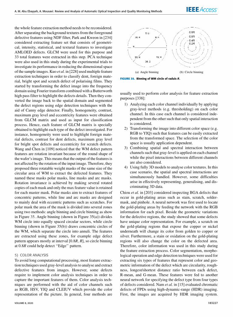
A. M. Abu Ebayyeh, A. Mousavi: Review and Analysis of Automatic Optical Inspection and Quality Monitoring Methods
the whole feature extractionmethod needs to be reconsidered.After separating the background textures from the foregrounddefective features using NDF filter, Park and Kweon in [234]considered extracting feature set that consists of geometri-cal, intensity, statistical, and textural features to investigateAMLOED defects. GLCM were used for this purpose and33 total features were extracted in this step. PCA techniquewere also used in this study during the experimental trials toinvestigate its performance in reducing the dimensional spaceof the sample images. Kuo et al. in [228] usedmultiple featureextraction techniques in order to classify dent, foreign mate-rial, bright spot and scratch defect of polarising films. Theystarted by transforming the defect image into the frequencydomain using Fourier transform combinedwith a Butterworthhigh pass filter to highlight the defects details. Then they con-verted the image back to the spatial domain and segmentedthe defect regions using edge detection techniques with theaid of Canny edge detector. Finally, homogeneity, contrast,maximum gray level and eccentricity features were obtainedfrom GLCM matrix and used as input for classificationprocess. Hence, each feature of GLCM matrix is speciallyobtained to highlight each type of the defect investigated. Forinstance, homogeneity were used to highlight foreign mate-rial defects, contrast for dent defects, maximum gray levelfor bright spot defects and eccentricity for scratch defects.Wang and Chen in [109] noticed that the WM defect patternfeatures are rotation invariant because of the round shape ofthewafer’s image. Thismeans that the output of the features isnot affected by the rotation of the input image. Therefore, theyproposed three rotatable weight masks of the same size of thecircular area of WM to extract the defected features. Theynamed these masks polar masks, line masks and arc masks.Rotation invariance is achieved by making several rotatedcopies of eachmask and only themax feature value is retainedfor each master mask. Polar masks aim to extract features ofconcentric patterns, while line and arc masks are designedto mainly deal with eccentric patterns such as scratches. Forpolar mask the area of the mask is divided into several zonesusing two methods: angle binning and circle binning as showin Figure 35. Angle binning (shown in Figure 35(a)) dividesWM circle into equally spaced circular sectors, while circlebinning (shown in Figure 35(b)) draws concentric circles ofthe WM, which separate the circle into annuli. The featuresare extracted using these zones, for example edge defectpattern appears mostly at interval [0.8R,R], so circle binningat 0.8R could help detect ‘‘Edge’’ pattern.
5) COLOR ANALYSISTo avoid long computational processing, most feature extrac-tion techniques used gray-level analysis to analyse and extractdefective features from images. However, some defectsrequire to implement color analysis techniques in order tocapture the important features of them. Color analysis tech-niques are performed with the aid of color channels suchas RGB, HSV, YIQ and CLEIUV which provide the colorrepresentation of the picture. In general, four methods are
FIGURE 35. Binning of WM circle of raduis R.
usually used to perform color analysis for feature extractionpurposes [338]:
1) Analyzing each color channel individually by applyinggray-level methods (e.g. thresholding) on each colorchannel. In this case each channel is considered inde-pendent from the other such that only spatial interactionis considered.
2) Transforming the image into different color space (e.g.RGB to YIQ) such that features can be easily extractedfrom the transformed space. The selection of the colorspace is usually application dependent.
3) Combining spatial and spectral interaction betweenchannels such that gray-level is applied on each channelwhile the pixel interactions between different channelsare also considered.
4) Using fully 3D models to analyse color textures. In thiscase scenario, the spatial and spectral interactions aresimultaneously handled. However, some difficultiesarise in effectively representing, generalising, and dis-criminating 3D data.
Chiou et al. in [203] considered inspecting BGA defects thatoccur in gold-plating areas such as stain, scratch, solder-mask, and pinhole. A neural network was first used to locatethe gold-plating areas by feeding the network with the RGBinformation for each pixel. Beside the geometric variationsfor the defective regions, the study showed that some defectshave unique color representation. For example, a scratch onthe gold-plating regions that expose the copper or nickelunderneath will change its color from golden to copper orsilver. Furthermore, a stain or oxidation on the gold-platingregions will also change the color on the defected area.Therefore, color information was used in this study duringthe feature extraction process. Color segmentation, morpho-logical operation and edge detection techniques were used forextracting six types of features that represent color and geo-metric information of the defect which are circularity, rough-ness, longest/shortest distance ratio between each defect,R-mean, and G-mean. These features were fed to anotherneural network for specifying the defect type from four typesof defects considered. Nam et al. in [15] evaluated chromaticdefects of FPDs using high-dynamic-range (HDR) imaging.First, the images are acquired by HDR imaging system.
VOLUME 8, 2020 183227
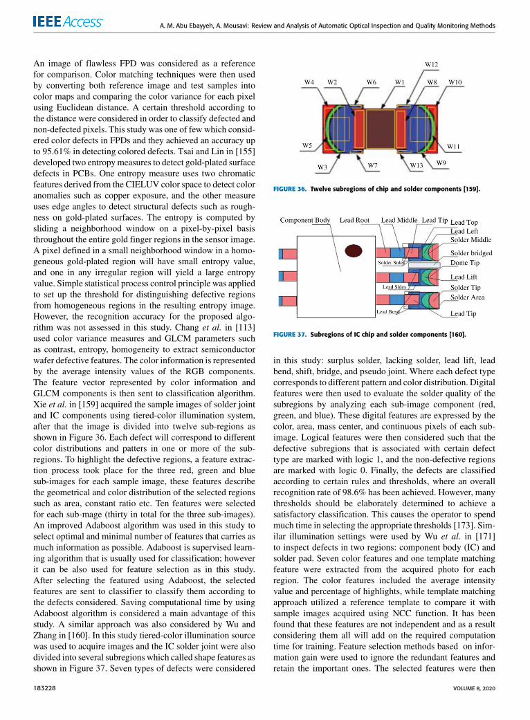
A. M. Abu Ebayyeh, A. Mousavi: Review and Analysis of Automatic Optical Inspection and Quality Monitoring Methods
An image of flawless FPD was considered as a referencefor comparison. Color matching techniques were then usedby converting both reference image and test samples intocolor maps and comparing the color variance for each pixelusing Euclidean distance. A certain threshold according tothe distance were considered in order to classify defected andnon-defected pixels. This study was one of few which consid-ered color defects in FPDs and they achieved an accuracy upto 95.61% in detecting colored defects. Tsai and Lin in [155]developed two entropymeasures to detect gold-plated surfacedefects in PCBs. One entropy measure uses two chromaticfeatures derived from the CIELUV color space to detect coloranomalies such as copper exposure, and the other measureuses edge angles to detect structural defects such as rough-ness on gold-plated surfaces. The entropy is computed bysliding a neighborhood window on a pixel-by-pixel basisthroughout the entire gold finger regions in the sensor image.A pixel defined in a small neighborhood window in a homo-geneous gold-plated region will have small entropy value,and one in any irregular region will yield a large entropyvalue. Simple statistical process control principle was appliedto set up the threshold for distinguishing defective regionsfrom homogeneous regions in the resulting entropy image.However, the recognition accuracy for the proposed algo-rithm was not assessed in this study. Chang et al. in [113]used color variance measures and GLCM parameters suchas contrast, entropy, homogeneity to extract semiconductorwafer defective features. The color information is representedby the average intensity values of the RGB components.The feature vector represented by color information andGLCM components is then sent to classification algorithm.Xie et al. in [159] acquired the sample images of solder jointand IC components using tiered-color illumination system,after that the image is divided into twelve sub-regions asshown in Figure 36. Each defect will correspond to differentcolor distributions and patters in one or more of the sub-regions. To highlight the defective regions, a feature extrac-tion process took place for the three red, green and bluesub-images for each sample image, these features describethe geometrical and color distribution of the selected regionssuch as area, constant ratio etc. Ten features were selectedfor each sub-mage (thirty in total for the three sub-images).An improved Adaboost algorithm was used in this study toselect optimal and minimal number of features that carries asmuch information as possible. Adaboost is supervised learn-ing algorithm that is usually used for classification; howeverit can be also used for feature selection as in this study.After selecting the featured using Adaboost, the selectedfeatures are sent to classifier to classify them according tothe defects considered. Saving computational time by usingAdaboost algorithm is considered a main advantage of thisstudy. A similar approach was also considered by Wu andZhang in [160]. In this study tiered-color illumination sourcewas used to acquire images and the IC solder joint were alsodivided into several subregions which called shape features asshown in Figure 37. Seven types of defects were considered
FIGURE 36. Twelve subregions of chip and solder components [159].
FIGURE 37. Subregions of IC chip and solder components [160].
in this study: surplus solder, lacking solder, lead lift, leadbend, shift, bridge, and pseudo joint. Where each defect typecorresponds to different pattern and color distribution. Digitalfeatures were then used to evaluate the solder quality of thesubregions by analyzing each sub-image component (red,green, and blue). These digital features are expressed by thecolor, area, mass center, and continuous pixels of each sub-image. Logical features were then considered such that thedefective subregions that is associated with certain defecttype are marked with logic 1, and the non-defective regionsare marked with logic 0. Finally, the defects are classifiedaccording to certain rules and thresholds, where an overallrecognition rate of 98.6% has been achieved. However, manythresholds should be elaborately determined to achieve asatisfactory classification. This causes the operator to spendmuch time in selecting the appropriate thresholds [173]. Sim-ilar illumination settings were used by Wu et al. in [171]to inspect defects in two regions: component body (IC) andsolder pad. Seven color features and one template matchingfeature were extracted from the acquired photo for eachregion. The color features included the average intensityvalue and percentage of highlights, while template matchingapproach utilized a reference template to compare it withsample images acquired using NCC function. It has beenfound that these features are not independent and as a resultconsidering them all will add on the required computationtime for training. Feature selection methods based on infor-mation gain were used to ignore the redundant features andretain the important ones. The selected features were then
183228 VOLUME 8, 2020
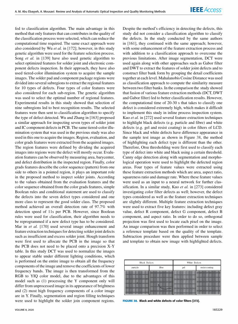
A. M. Abu Ebayyeh, A. Mousavi: Review and Analysis of Automatic Optical Inspection and Quality Monitoring Methods
fed to classification algorithm. The main advantage in thismethod that only features that can contributes in the quality ofthe classification process were selected, which can reduce thecomputational time required. The same exact approach werealso considered by Wu et al. in [172]; however, in this studygenetic algorithm were used for the feature selection process.Song et al. in [139] have also used genetic algorithm toselect optimized features for solder joint and electronic com-ponent defects inspection. In their approach, they have alsoused tiered-color illumination system to acquire the sampleimages. The solder pad and component package regions weredivided into several subregions to extract the regional featuresfor 10 types of defects. Four types of color features werealso considered for each sub-region. The genetic algorithmwas used to select the optimal number of regional features.Experimental results in this study showed that selection ofnine subregions led to best recognition results. The selectedfeatures were then sent to classification algorithm to specifythe type of defect detected. Wu and Zhang in [163] proposeda similar approach for inspecting seven types of solder jointand IC component defects in PCB. The same tiered-color illu-mination system that was used in the previous study was alsoused in this one to acquire the images. Region, evaluation, andcolor grads features were extracted from the acquired images.The region features were defined by dividing the acquiredimages into regions were the defect will mostly occur. Evalu-ation features can be observed by measuring area, barycenter,and defect distribution in the inspected region. Finally, colorgrads features describe the color sequence (pattern) from oneside to others in a pointed region, it plays an important rolein the proposed method to inspect solder joints. Accordingto the values obtained from the evaluation features and thecolor sequence obtained from the color grads features, simpleBoolean rules and conditional statement are used to classifythe defects into the seven defect types considered and onemore class to represent the good solder class. The proposedmethod achieved an overall detection rate of 97.7% withdetection speed of 11s per PCB. However, since Booleanrules were used for classification, their algorithm needs tobe reprogrammed if a new defect type has to be considered.Mar in et al. [170] used several image enhancement andfeature extraction techniques for detecting solder joint defectssuch as insufficient and excess solder joint. Hough transformwere first used to allocate the PCB in the image so thatthe PCB does not need to be placed onto a precision X-Ytable. In this study DCT was used to normalize the imagesto appear stable under different lighting conditions, whichis performed on the entire image to obtain all the frequencycomponents of the image and remove the coefficients of lowerfrequency bands. The image is then transformed from theRGB to YIQ color model, due to the advantages of thismodel such as (1) processing the Y component only willdiffer from unprocessed image in its appearance of brightnessand (2) most high frequency components of a color imageare in Y. Finally, segmentation and region filling techniqueswere used to highlight the solder join component regions.
Despite the method’s efficiency in detecting the defects, thisstudy did not consider a classification algorithm to classifythe defects. In the study conducted by the same authorsin [161], they continued with the same approach; however,with some enhancement of the feature extraction process andwith addition to a classification approach to overcome theprevious limitations. After image segmentation, DCT wereused again along with other approaches such as Gabor filterand DWT to extract the features of solder joint defects and toconstruct filter bank form by grouping the detail coefficientstogether at each level.Mahalanobis Cosine Distance was usedas classification approach to compute the similarity measurebetween two filter banks. In the comparison the study showedthat fusion of various feature extraction methods (DCT, DWTand Gabor filter) led to better classification results. However,the computational time of 20-30 s that takes to classify onedefect is considered extremely high, which makes it difficultto implement this study in inline process inspection system.Kuo et al. in [272] used several feature extraction techniquesto highlight black defects (e.g. particle and fibre) and whitedefects (e.g. gel and resist coating) in color filters of LCD.Since black and white defects have difference appearance inthe sample test image as shown in Figure 38, the methodof highlighting each defect type is different than the other.Therefore, Otsu thresholding were first used to classify eachtype of defect into white and black using a certain threshold.Canny edge detection along with segmentation and morpho-logical operation were used to highlight the defected regionareas. Four types of feature values were extracted usingthese feature extraction methods which are area, aspect ratio,squareness ratio and damage rate. Where these feature valueswere used as an input to a neural network for further clas-sification. In a similar study, Kuo et al. in [273] consideredinvestigating color filter defects as well; however, the defecttypes considered as well as the feature extraction techniquesare slightly different. Multiple feature extraction techniqueswere used to extract five key features: including defect grayvalue, defect R component, defect G component, defect Bcomponent, and aspect ratio. In order to do so, orthogonalprojection was first used to locate each pixel on the image.An image comparison was then performed in order to selecta reference template based on the quality of the template.Subtraction procedure were then applied between sampleand template to obtain new image with highlighted defects.
FIGURE 38. Black and white defects of color filters [272].
VOLUME 8, 2020 183229
A. M. Abu Ebayyeh, A. Mousavi: Review and Analysis of Automatic Optical Inspection and Quality Monitoring Methods
Control limits were then used to separate the defected regionsfrom the non-defected. Finally, segmentation and morpho-logical operations were implemented to extract the five keyfeatures that will be used as an input to classifier for defectclassification process.
6) MODEL-BASED FEATURE EXTRACTIONModel-based feature extraction methods are based on theconstruction of an image model that can be used to describea feature and synthesize it. The model parameters capturethe essential perceived qualities of feature [339]. Chen et al.in [76] proposed an algorithm based on a growing wavelethidden Markov tree (gHMT) statistical model to extract WMdefect patterns. The hierarchical tree-based model, gHMT,utilizes the growing and learning procedure to increase suc-cessively the size of the wavelet tree for better feature extrac-tion performance. Maximum likelihood classifier were thenused to classify the patterns detected into four classes: annu-lus, half-annulus, band and half-ring. Jiang et al. in [178]proposed a model approach to classify solder paste defectsbased on learning the color biological feature sub-manifold.The biologically inspired color feature (BICF) is appliedto represent the solder paste images by generating featuremaps and introduce a new sub-manifold learning method toextract the intrinsic low-dimensional BICF manifold embed-ded in an extrinsic high-dimensional ambient space. Thisapproach can simulate the optical inspection task performedby human inspector by identifying poor from good qualitysolders. The output for the BICF approach in then fed toclassifier for the classification process. However, this methodcannot analyse the details of the defects effectively [139].Xie et al. in [31] proposed a model-based approach to detectdefective pixels in PCB sample images, the model conductedin this study is called localized defects image model (LDIM).In manual inspection task, workers focus on the local defectsrather than global defects by considering both regional colordeviation from the local dominant color and regional colorrapidly changing as possible defects. This model can mimicthe manual inspection process by considering two main fac-tors: color deviation and color fluctuation. An ROI of size100 - 1000 pixels is extracted from the original image so thatthe LDIM model can be applied by identifying local differ-ences in color between potential defects in the foregroundand the background. A specific threshold was used then toclassify each pixel as defective and non-defective. Second,labelling and blob analysis are performed to characterize theshape and size of the defects. In this step, the labelling of eightconnected components was calculated and a particular areathreshold value was applied to each of these images. Theirproposed method achieved 100% detection rate with zerofalse alarm. It is also worth mentioning that their approachoutperformed template matching approaches by analyzingcolor variations and color-related defects. Furthermore, it candetect tiny defect embedded in a pad image that may dif-fer only slightly from the surrounding region. However,their approach cannot classify the PCB defect by type and
therefore it cannot be considered fully automated for inspec-tion purposes. Lu et al. in [209] used model-based approachand thermography to inspect solder ball defects such as miss-ing balls in BGAs. Thermography can help in detecting theheat changes as a result of the defect in the thermal images,such that each defect has its own heat signature. Furthermore,location and size of the defect can be easily determined usingthis technique. The details of constructing the thermographydetection system for this study was already discussed inearlier study conducted by the same authors in [319]. In orderto improve the signal-to-noise ratio, mathematical modelbased on polynomial fit and differential absolute contrasttechniques were utilized to reconstruct the thermal images.Three statistical feature vectors were then extracted from thereconstructed images that represent the area of the solder ball,the variance of the hot spots and temperature. The three vec-tors are then sent for classification algorithm to classify thedefects. Despite the effectiveness of thermography to detectcertain types of defects, this method has relatively low spatialresolution (typically 640 × 480 pixels), which makes it notsuitable for small defects detection that requires high resolu-tion [340]. Jiang et al. in [238] proposed statistical modelsto identify Mura defects in TFT-LCD in addition to theirsizes and locations. This study used luminance meter (lightsensitive device) instead of a CCD device to measure panelsurface brightness in a darkroom environment with the panelswitched to white background. LCD panel is divided into144 areas. Five points are measured to obtain the luminancedata. Using the acquired data, Analysis of Variance (ANOVA)were implemented to identify areas significantly differentfrom other areas in a panel. A certain threshold was definedaccording to the luminance, such that if the value exceeds thethreshold, the sample is considered non-defective. Otherwise,the sample is considered to have Mura defect and a furtherstep is required to identify the location and size of the defect.Exponentially Weighted Moving Average (EWMA) controlchart concepts were used to detect the non-uniformity areasin a panel and to identify the location of Mura defects alongwith their sizes. Despite the capability and simplicity oftheir method to identify the defect type, location, and size,several limitations have been observed in their study. Theirproposed procedure was limited to 15-inch LCD panels asproduced by a local manufacturer. Furthermore, the methodused for acquiring data limited their ability to identify adefective area partially overlapping two or more of the testingsamples. Finally, certain parameter that was important tocalculate EWMA, was estimated by trial and error, whichmake their method not fully automated. Another statisticalapproach that were used to accelerate defect detection processcalled multivariate Hotelling T-squared statistics. Hong-DarLin used this method extensively in his research articlesto highlight defects in LEDs [36], [38], LCDs [245], andceramic capacitor chips [291], [292]. After dividing the imageinto several sub-images using image masks, feature vectorscan be obtained using wavelet analysis as in [36], [291],[292], energy features as in [38] or color models as in [245].
183230 VOLUME 8, 2020
A. M. Abu Ebayyeh, A. Mousavi: Review and Analysis of Automatic Optical Inspection and Quality Monitoring Methods
These feature vectors are used to construct what so calledT 2 distance or T 2 value. T 2 value can be regarded as adistance value of amultivariate processing unit. The larger theT 2 statistic value, the more distinctive the region is from thenormal area. Thus, the more easily the region can be judgedas defective. Owing to the blurriness and low contrast natureof Mura defects in LCDs, Gan and Zhao in [219] proposeda modified local binary fitting model (LBF) to highlightthe defected regions. LBF models are considered one of thesegmentation techniques that can solve the problem causedby intensity inhomogeneity [341]. The proposed modifiedLBF model made robust to initial contour and competent forthe extraction of defect boundaries. Furthermore, in orderto detect multiple defects with different brightness levels,the study introduced a simple processing scheme to narrowthe brightness range of defects based on statistical threshold-ing. Their method achieved a very high recognition rate alongwith low false alarm rated comparedwith othermethod. How-ever, this method is considered computational expensive andless efficient compared with similar methods such as Markovconcurrent vision (MCV) and independent component analy-sis (ICA). Bi et al. in [242] proposed a level set based methodfor segmenting Mura defects with a new region-based activecontour model, which is an improvement on the Chan-Vesemodel. Chan-Vese model is an active contour model whichuses region based information rather than the gradient of theimage. Thus, the objects whose boundaries are not definedby gradients or have very smooth boundaries can be detectedand the position of the initial curve can be anywhere in theimage even not surrounding the objects [342]. In this study,Gabor filter were first used to remove the background then theproposedmodel was used for defect identification. The defectdetecting rate of this study was relatively high (up to 96%).However, some drawbacks were observed on this study. Forinstance, the proposed model is based on the assumptionthat image intensities are statistically homogeneous in eachregion and thus is not suitable for small Mura defects withuneven backlight and cannot be applied in online displayinspection due to its very large search space and excessivetime consumption [219], [243]. Also, how to choose theparameters of model was still not a standard of theoreticalknowledge as a guide [284]. Furthermore, the proposed studydid not include a classification algorithm to automaticallyclassify the defects. Yang et al. in [243] proposed similarapproach to investigate Mura defects in FPDs. The methodproposed consisted of two parts: an outlier-prejudging-basedimage background construction (OPBC) algorithm which isintended to quickly reduce the influence of image back-grounds with even brightness and to coarsely estimate thecandidate regions of Mura defects. Then, region-gradient-based level set (RGLS) algorithm is applied only to these can-didate regions to segment the contours of the Mura defects.The algorithms used in this study were compared to similaralgorithm such as the one used in [242] and it showed betterperformance in terms of accuracy and false alarm values.Moreover, the model proposed in [242] requires almost 500s
of computational time which is more than 40 times slowercompared with the algorithm used in this study. Lee and Yooin [237] proposed a complicated data fitting approach basedon regression to detect region-Mura defects with unevenbrightness in TFT-LCD. The study estimated the backgroundregion of the sample image modified regression diagnostics,then the background region was approximated by a low orderpolynomial to generate a background surface. The reasonbehind this procedure is to perform subtraction process forthe background from the original image. This subtraction canremove the influence of non-uniform background and trans-form the segmentation problem into a simple thresholdingone. The resulting image is then post-processed by medianfiltering, morphological closing, and morphological openingto remove noise and refine the segmentation result. Finally,a certain threshold was used according to the gray-level inten-sity, which can be adjusted according to the panel qualityto classify the defective samples. The experimental resultsshowed that the proposed method succeeded in detectingthe region-Mura defects. However, it is very computationallyintensive because the background surface must be estimatedrecursively by eliminating one pixel at a time throughout theentire inspection image [265]. Chen and Chang in [239] usedthe same approach as the previous study; however, the orderof the polynomials used in the regression process was speci-fied. The detection rate of Mura defects achieved in this studywas over 90.9% and the number of defects and the achievedrate of defects on each panel may reach 100%. In anothersimilar study, Fan and Chuang in [247] proposedMura defectdetection algorithm based on regression diagnostics. Thesample images were converted to gray-level data, this pro-cess was accelerated by dividing the image into several sub-images. Gray-level data are then modelled using the linearregression model. Prediction error sum of squares were thenestimated to filter out theMura defects. Image morphologicaldilation techniques were used to identify defected neighborpixels. Finally, the differences of all the gray-level values(including Mura and non- Mura pixels) between original andestimated images are filtered by using a threshold and SPCmethod to classify the defects. If the difference is greaterthan the threshold, then the pixel is classified as Mura pixel.This method has the advantage of performing the inspectionin relatively low processing time with low false alarm rates.Despite of these advantages this method cannot detect defectswith sub-pixel accuracy [315]. Ngo et al. in [220] performedbackground reconstruction to extract the features of differentmura defects in TFT-LCD. Several algorithms were used forthis purpose such as DCT, polynomial surface fitting and seg-mentation. The usage of polynomial surface fitting and DCTwas according to the size ofmura defect such that if the size ofthe mura defect is small (according to predefined threshold)compared with the image, then polynomial surface fittingis used for background reconstruction. Otherwise, DCT isused for background reconstruction. Based on the sensitivityof the human eye to Mura defect, the level for each Muracandidate is quantified using the concept of just-noticeable
VOLUME 8, 2020 183231
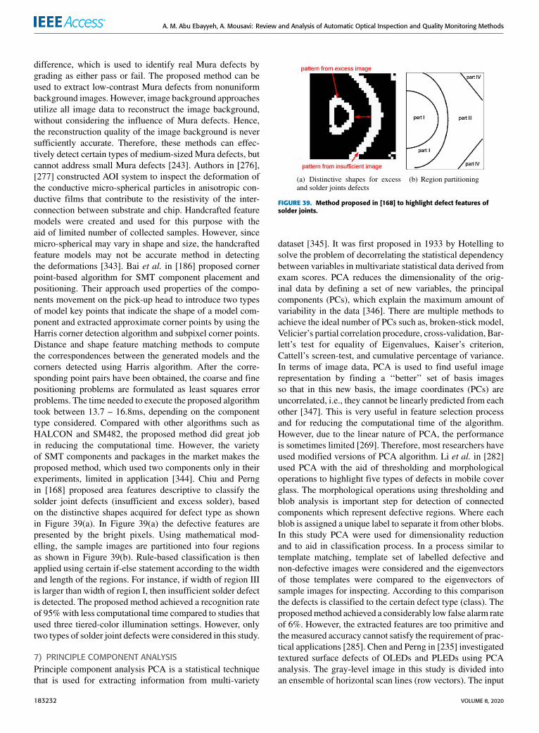
A. M. Abu Ebayyeh, A. Mousavi: Review and Analysis of Automatic Optical Inspection and Quality Monitoring Methods
difference, which is used to identify real Mura defects bygrading as either pass or fail. The proposed method can beused to extract low-contrast Mura defects from nonuniformbackground images. However, image background approachesutilize all image data to reconstruct the image background,without considering the influence of Mura defects. Hence,the reconstruction quality of the image background is neversufficiently accurate. Therefore, these methods can effec-tively detect certain types of medium-sized Mura defects, butcannot address small Mura defects [243]. Authors in [276],[277] constructed AOI system to inspect the deformation ofthe conductive micro-spherical particles in anisotropic con-ductive films that contribute to the resistivity of the inter-connection between substrate and chip. Handcrafted featuremodels were created and used for this purpose with theaid of limited number of collected samples. However, sincemicro-spherical may vary in shape and size, the handcraftedfeature models may not be accurate method in detectingthe deformations [343]. Bai et al. in [186] proposed cornerpoint-based algorithm for SMT component placement andpositioning. Their approach used properties of the compo-nents movement on the pick-up head to introduce two typesof model key points that indicate the shape of a model com-ponent and extracted approximate corner points by using theHarris corner detection algorithm and subpixel corner points.Distance and shape feature matching methods to computethe correspondences between the generated models and thecorners detected using Harris algorithm. After the corre-sponding point pairs have been obtained, the coarse and finepositioning problems are formulated as least squares errorproblems. The time needed to execute the proposed algorithmtook between 13.7 – 16.8ms, depending on the componenttype considered. Compared with other algorithms such asHALCON and SM482, the proposed method did great jobin reducing the computational time. However, the varietyof SMT components and packages in the market makes theproposed method, which used two components only in theirexperiments, limited in application [344]. Chiu and Perngin [168] proposed area features descriptive to classify thesolder joint defects (insufficient and excess solder), basedon the distinctive shapes acquired for defect type as shownin Figure 39(a). In Figure 39(a) the defective features arepresented by the bright pixels. Using mathematical mod-elling, the sample images are partitioned into four regionsas shown in Figure 39(b). Rule-based classification is thenapplied using certain if-else statement according to the widthand length of the regions. For instance, if width of region IIIis larger than width of region I, then insufficient solder defectis detected. The proposed method achieved a recognition rateof 95%with less computational time compared to studies thatused three tiered-color illumination settings. However, onlytwo types of solder joint defects were considered in this study.
7) PRINCIPLE COMPONENT ANALYSISPrinciple component analysis PCA is a statistical techniquethat is used for extracting information from multi-variety
FIGURE 39. Method proposed in [168] to highlight defect features ofsolder joints.
dataset [345]. It was first proposed in 1933 by Hotelling tosolve the problem of decorrelating the statistical dependencybetween variables in multivariate statistical data derived fromexam scores. PCA reduces the dimensionality of the orig-inal data by defining a set of new variables, the principalcomponents (PCs), which explain the maximum amount ofvariability in the data [346]. There are multiple methods toachieve the ideal number of PCs such as, broken-stick model,Velicier’s partial correlation procedure, cross-validation, Bar-lett’s test for equality of Eigenvalues, Kaiser’s criterion,Cattell’s screen-test, and cumulative percentage of variance.In terms of image data, PCA is used to find useful imagerepresentation by finding a ‘‘better’’ set of basis imagesso that in this new basis, the image coordinates (PCs) areuncorrelated, i.e., they cannot be linearly predicted from eachother [347]. This is very useful in feature selection processand for reducing the computational time of the algorithm.However, due to the linear nature of PCA, the performanceis sometimes limited [269]. Therefore, most researchers haveused modified versions of PCA algorithm. Li et al. in [282]used PCA with the aid of thresholding and morphologicaloperations to highlight five types of defects in mobile coverglass. The morphological operations using thresholding andblob analysis is important step for detection of connectedcomponents which represent defective regions. Where eachblob is assigned a unique label to separate it from other blobs.In this study PCA were used for dimensionality reductionand to aid in classification process. In a process similar totemplate matching, template set of labelled defective andnon-defective images were considered and the eigenvectorsof those templates were compared to the eigenvectors ofsample images for inspecting. According to this comparisonthe defects is classified to the certain defect type (class). Theproposedmethod achieved a considerably low false alarm rateof 6%. However, the extracted features are too primitive andthemeasured accuracy cannot satisfy the requirement of prac-tical applications [285]. Chen and Perng in [235] investigatedtextured surface defects of OLEDs and PLEDs using PCAanalysis. The gray-level image in this study is divided intoan ensemble of horizontal scan lines (row vectors). The input
183232 VOLUME 8, 2020

A. M. Abu Ebayyeh, A. Mousavi: Review and Analysis of Automatic Optical Inspection and Quality Monitoring Methods
spatial domain image is then transformed into principal com-ponent space so that the directional textures are well approx-imated by first major components and their correspondingweight vectors (named truncated component solution (TCS)).TCS are determined by first normalising eigenvalues of eachimage and then retain only those components whose nor-malized eigenvalue are greater than one. Subtraction pro-cess were then applied between TCS and original image toreveal the defective features and blur all directional textures.Finally, thresholding with the aid of SPC chart were appliedto classify the defects. The proposed has major advantages ofbeing insensitive to horizontal and vertical shifting, changesin illumination, and image rotation. However, the methodproposed in this study is not suitable to deal with high reso-lution image because the inherent complexity of PCA [348].Furthermore, it is not suitable for detecting relatively largedefects since large defects seriously destroy the regularityof texture. Tsai et al. in [267] proposed PCA-based methodcalled Integral Image for defect detection in non-textured andhomogeneously textured images such as LCD panel back-light and solar wafers. Compared to conventional PCA, thismethod can increase the computation speed of eigenvalues.The method consists of a small neighborhood window thatslides over the inspected image and for each window theregularity measure is then derived from the PCA. Two mainparameters were used in the algorithm that plays vital role inthe detection performance; control constant K which definesthreshold value for detection, and sliding window size forthe sample image. Since this paper deals with many surfacedefects (e.g. solar wafers and backlight), the value of optimalK may very according to the application; however, a valueof 3 has been demonstrated to perform well in most appli-cations. A proper value of the window size has major rolein determining how accurate and efficient the algorithm is.A small window size such as 25 × 25 or less detects onlypartial defects or defect edges. Conversely, an excessivelylarge window size with respect to the defect size may smooththe detected region and omit subtle defects or small-sizeddefects. Therefore, in this study window sizes between31× 31 and 61× 61 can well detect the presence of defectsfor most of the defects considered. Compared with othermethod such as Fourier transform, this method is consideredrelatively fast as it needs only 0.032 s to process sample imagecompared with 0.172 s in Fourier transform. Zervakis et al.in [182] performed post-placement inspection of SMDon PCBs. The developed approach involves the indirect mea-surement of each lead displacement with respect to its idealposition, centralized on its pad region. This displacement isinferred from area measurements on the image data of thelead region through a classification process. Sample imagesof the proposed approach were a mixture of acquired imagesvia hardware optical inspection setup (CCD and illuminationdevices) and Monte-Carlo simulated images. After definingthe ROIs and performing geometrical transformation, a four-level Otsu thresholding is applied on each ROI, to segmentthe lead images that are included in the examined ROI image.
This process will aid to extract twelve features for the leadregion that represent area and geometrical measurements ofthe regions. To reduce the dimension of the feature vec-tor that contains the twelve features, Karhunen-Loeve trans-formation (similar to PCA) is used for this purpose. Thereduced features were finally sent to classification algorithm.Goumas et al. in [183] proposed a similar approach thatfurther improves the positioning measurements of individualleads by means of information fusion and multiple classifi-cation. In this study, three sets of features are extracted fromeach segmented lead image, which represent different char-acteristics. The first set represents optical characteristics bymeans of simple area measures that sustain the most desirableimage attributes. The second set reflects only the edge infor-mation, whereas the third set pertains to features derived fromthe one-dimensional projection profile of the lead image inone direction. Liu et al in [269] proposed a nonlinear versionof PCA, called kernel PCA (KPCA) to investigate defectsduring GE stage in TFT-LCD manufacturing. KPCA cancapture the nonlinear relationships between pixels, extractmore discriminating features, and reduce the dimensionalityof the input image. KPCA has shown to have better per-formance than PCA in terms of feature extraction in otherapplications such as in face recognition [349]. In this study,segmentation and KPCA were used to highlight the defectiveareas in the pixel region of GE pattern. The feature vectorwas then sent to an input to a classifier to further identifythe category of the highlighted defect. Despite of overcomingthe PCAmain disadvantage due to linear behaviour, KPCA isconsidered computationally expensive since the kernel matrixneeds to be stored after the training, and as a test datumarrives, a large number of dot-product calculations is neededto obtain the projection of the test datum [268]. Liu et al.in [268] proposed a powerful non-linearity dimensionalityreduction technique called locally linear embedding (LLE) todeal with the large-input-dimensionality in the image datasetof GE defects in TFT-LCD. After performing the segmen-tation process to locate the defective regions in the imagesamples, LLE can map the high-dimensional input data intoa single low-dimensional embedding coordinate system bymanifold learning. By LLE, the input dimensionality of theclassifier can be reduced substantially, therefore reducing thecomplexity of the classifier. This method overcomes similarnon-linear dimensionality methods such as KPCA in terms ofthe reduced computational time. Cai et al. in [174] proposeda modified PCA technique to inspect IC solder joint defectscalled Robust Principle Component Analysis (RPCA). Theirprocedure starts by decomposing a set of qualified IC jointsimages and tested samples of IC solder joints images intolow-rank component and an error component using RPCA.Hence, the data used for RPCA is acquired from hue channelof the image, since hue channel contains major informa-tion for color. Then, a defect score (threshold) is definedbased on the appearance model and used to evaluate thequality of IC solder joints. Location prior knowledge is alsoused to enhance the defect score selection. Their proposed
VOLUME 8, 2020 183233

A. M. Abu Ebayyeh, A. Mousavi: Review and Analysis of Automatic Optical Inspection and Quality Monitoring Methods
method showed similar results to ViBE algorithm (proposedby the same authors in [173]) in the case of inspecting qual-ified ICs. However, in the case of unqualified IC inspec-tion the proposed method outperformed ViBE algorithm.Despite of the previous observations, the proposed studyfaced some limitations such high computational time whichcan be partially solved by employing hardware accelerationand parallel computing. Moreover, their approach classifiedsolder joints defects as qualified and unqualified withoutusing classification approach to specify the type of defect.Lai et al. in [224] used RPCA algorithm as well for detectingaesthetic polarizer defects with the aid of structured illumi-nation. Their algorithm achieved up to 99% detection rate.The algorithm was also capable of detecting other type ofdefect that were not intended to be detected such as dust,stains, and scratches. Despite of RPCA’s robust behaviourto outliers [350], RPCA is considered a very complicatedmathematical model. According to Cai et al. in [175], thereis no report of using RPCA in real industrial applications.
Cen et al. in [254] used low-rank matrix reconstructiontechnique, which is considered a similar method to RPCA,along with segmentation to highlight surface defect featuresin TFT-LCDpanel. In this algorithm, the textured backgroundof the sample image is considered the low-rank matrix, whilethe foreground image with defect can be treated as sparsematrix. The defective region in this study is considered tinycompared with the whole image. However, if the defectedregion is relatively large, this may be reflected to the back-ground features and will affect the background reconstructionmethod [351]. Furthermore, this method can only solve LCDimages with simple background [352].
Similar to PCA, Singular Value Decomposition (SVD) isanother linear method used to extract the significant featurecomponents of the image, which can be also used to calculatePCs. This applies by considering the image as a matrix sothat eigenvectors of an image matrix (eigen-images) can beobtained. Eigen-images are then used to calculate singularvalues (which represent feature data of the image). Only therelevant parts of the singular values need to be retained asthe compressed data for reconstructing the original images.The local, detailed information can be truncated to elimi-nate the redundancy of image compression [258]. Lu andTsai in [257], [258] investigated micro-defects such as pin-hole, scratches, particles and fingerprints in TFT-LCD usingSVD. The singular values which represent the backgroundwere selected. The image was then reconstructed without theselected singular values in order to eliminate the effect of thebackground and highlight the defective regions (anomalies)in the foreground. SPC were used to set up the control lim-its for distinguishing defects from the uniform region. Thismethod is suitable for detecting defects of highly periodictextured surfaces; however, the variety of LCDmanufacturingprocesses and the higher image resolutions of LCD prod-ucts often lead to less periodical, more complicated texturalstructures in sensed images [245]. Furthermore, the proposedmethod is highly sensitive to texture direction and face
difficulties in separating faint and large defects such as Murafrom the texture background [242], [286]. Kim et al. in [99]used Regularized Singular Value Decomposition (RSVD)method, which is based on SVD, as a feature extrac-tion approach to extract failure patterns of DRAM WBM.The benefit of the proposed RSVD is to obtain binaryeigen-images from a binary matrix of WBM. Each resultedeigen-image represents different defect pattern of the failedchips of WBM, thus the matrix norm of the eigen-image isequivalent to the contribution that the failure patterns of eacheigen-image make to WBM. Finally, the detected patternsare classified using K-means clustering to specify the defecttype.
Another technique which is considered a generalization ofPCA called Independent Component Analysis (ICA) is con-sidered in literature. ICA is a method of extraction of statisti-cally independent signals (called sources) from observed lin-ear mixtures, to generate simultaneously observed sequencesof data (de-mixing matrix) without any prior knowledgeof the mixing mechanisms. This method is widely used indealing with medical signals and telecommunication [246],[353]. Tsai et al. in [265] investigated backlight module andglass substrate small defects in low-contrast uniform surfaceimages. For this purpose, they proposed a constrained ICAmodel with the aid of PSO algorithm to design an optimalfilter with the objective that the convolution filter will gen-erate the most representative source intensity of the back-ground surface without noise. Therefore, by sliding the filterin the inspection image, all pixels in non-defected regionswill have approximately the same impulse responses, whilethe pixels in defective regions have distinct responses in thefiltered image. Certain control limits were used to classify thedefective regions from the non-defected ones. Experimentalresults from the backlight panels and LCD glass substrateshave shown that the proposed ICA-based filtering scheme caneffectively detect various small defects in low-contrast sur-face images. However, the convolution filtering scheme can-not work effectively for the detection of large-sized defectssuch as gravity-Mura since the defective region is too largeto be confined in a limited filter window, and sliding a verylarge filter window pixel by pixel in the image is computa-tionally expensive [246]. Tsai and Lai in [354] used ICA tohighlight defected features in periodic complex patters suchas TFT-LCD panels and color filter. In this study, the sam-ple images were scanned top-down direction by horizontalscanning and was transformed into 1D image. The result-ing 1D image was then divided into two segments of equallength. ICA were then applied and de-mixing matrix of size2 × 2 were obtained with the aid of probability densityfunction (PDF) and PSO algorithm to recover the translationbetween the two divided segments. Finally, NCC templatematching were applied to compare between the divided seg-ments and detect defects incase an abnormality was detected.Due to the small size of the de-mixing matrix used, thismethod is considered computationally efficient, which makeson-line, real-time implementation of the proposed method for
183234 VOLUME 8, 2020
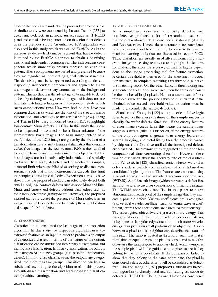
A. M. Abu Ebayyeh, A. Mousavi: Review and Analysis of Automatic Optical Inspection and Quality Monitoring Methods
defect detection in a manufacturing process become possible.A similar study were conducted by Lu and Tsai in [355] todetect micro-defects in periodic surfaces such as TFT-LCDpanel and can also be implemented on the color filter defectsas in the previous study. An enhanced ICA algorithm wasalso used in this study which was called FastICA. As in theprevious study, each 1D image segment that has no defectsis trained by the FastICA algorithm to obtain a de-mixingmatrix and independent components. The independent com-ponents which show spiky profiles represent an edge of apattern. These components are sorted and preserved becausethey are regarded as representing global pattern structures.The de-mixing matrix is regenerated according to the cor-responding independent components and applied to a newtest image to determine any anomalies in the backgroundpattern. This method has the advantage of being able to detectdefects by training one segmented image and it does not usetemplate matching techniques as in the previous study whichsaves computational time. However, both studies have twocommon drawbacks which are the loss of the size and shapeinformation, and sensitivity to the vertical shift [234]. Tsengand Tsai in [246] used a modified version ICA to highlightlow-contrast Mura defects in LCDs. In this study the imageto be inspected is assumed to be a linear mixture of therepresentative basis images. The basis images which havethe full size of the LCD image are given by the product of atransformation matrix and a training data matrix that containsdefect-free images as the row vectors. PSO is then appliedto find the transformation matrix under the objective that thebasis images are both statistically independent and spatiallyexclusive. To classify defected and non-defected samples,a control limit where established according to distance mea-surement such that if the measurements exceeds this limitthe sample is considered defective. Experimental results haveshown that the proposed method can effectively detect bothsmall-sized, low-contrast defects such as spot-Mura and line-Mura, and large-sized defects without clear edges such asthe hardly detectable gravity-Mura. However, the proposedmethod can only detect the presence of Mura defects in animage. It cannot be directly used to identify the actual locationand shape of a Mura defect.
C. CLASSIFICATIONClassification is considered the last stage of the inspectionalgorithm. In this stage the inspection algorithm uses theextracted features as an input in order to produce a an outputof categorized classes. In terms of the nature of the output,classification can be subdivided into binary classification andmulti-class classification. In binary classification, the outputsare categorized into two groups (e.g. pass/fail, defect/non-defect). In multi-class classification, the outputs are catego-rized into more than two groups. Classification can be alsosubdivided according to the algorithm used in this processinto rule-based classification and learning-based classifica-tion (machine learning).
1) RULE-BASED CLASSIFICATIONAs a simple and easy way to classify defective andnon-defective products, a lot of researchers used sim-ple logic classifiers such as conditional statement (if-else)and Boolean rules. Hence, these statements are consideredpre-programmed and has no ability to learn as the case inmachine learning tools that are discussed in section V-C2.These classifiers are usually used after implementing a rel-evant image processing technique to highlight the featuresfor analysis, therefore the accuracy of them is highly depen-dent on the image processing tool for feature extraction.A certain threshold is then used for the assessment process.For instance, in template matching this threshold is calledthe matching score. On the other hand, if thresholding andsegmentation techniques were used, then the threshold couldbe the number of bright pixels. Human assessor can define athreshold value for the previous thresholds such that if theobtained value exceeds threshold value, an action must bemade (e.g. consider the sample defective).
Shankar and Zhong in [122] set up a series of five logicrules based on the energy features of the sample images toclassify the wafer defects. Such that, if the energy featuresof error image exceeds 1µm, this means the sample imagesuggests a defect (rule 1). Further on, if the energy featuresof the chip-out region is greater than energy features ofscratch, bridging, and metal lifting then the defect is causedby chip-out (rule 2) and so until all the investigated defectsare classified. The previous study suggested a simple and lesscomputational time consuming algorithm. However, therewas no discussion about the accuracy rate of the classifica-tion. Yeh et al. in [128] classified semiconductor wafer diesdefects such as particle contamination and scratch based onconditional logic algorithm. The features are extracted usinga recent approach called wavelet transform modulus sum(WTMS). A golden sub-image (which represent a defect freesample) were also used for comparison with sample images.The WTMS approach is modified in this paper to detectabnormalities in each pixel of the sample image that may indi-cate a possible defect. Various coefficients are investigated(e.g. vertical wavelet coefficient and horizontal wavelet coef-ficient), were these coefficients are called ‘‘wavelet energy’’.The investigated object (wafer) preserve more energy thanbackground does. Furthermore, pixels on corners clusteringnoisy spots or irregular edges maintain much more waveletenergy than pixels on small portions of an object do. A ratiobetween a pixel and its neighbor can describe the status ofthis pixel. The ratio is treated as threshold, such that if it ismore than or equal to zero, the pixel is considered as a defectotherwise the sample goes to another check which comparesthe sample pixel with the golden sample pixel to see if theybelong to the same coordinate. If the comparison failed toshow that they belong to the same coordinate, the pixel isconsidered a defect, otherwise it will be considered as defect-free. Lim and Jeong in [261] proposed a rule-based inspec-tion algorithm to classify fatal and non-fatal glass substratedefects in TFT-LCD. The rules and thresholds considered
VOLUME 8, 2020 183235
A. M. Abu Ebayyeh, A. Mousavi: Review and Analysis of Automatic Optical Inspection and Quality Monitoring Methods
are based on the information of defect position, size, andgray-level. Despite of the low false alarm rate achieved inthis study; the overall accuracy is relatively low comparedwith other studies. In Ye et al. [176], after using the adaptivetemplate method, they used a conditional statement using athreshold to identify whether a pixel in the difference imageis a potential solder joint defect pixel or not. The threshold Ris defined based on the hue channel difference between thetemplate and sample image from the dictionary. Where R isan empirical threshold in the context, which is not sensitive tothe inspection performance. Cai et al. in [173] classified thehue channel value of an input pixel (sample) into qualifiedor unqualified one by comparing it with the templates. If thepixels of the samples are in the range of hue channel in anyof the defined templates, the sample is considered qualifiedand vice versa. The threshold that is used for classifying thedefects is called defect degree.
Fuzzy Logic which is a form of multi-valued logic wasalso one of the classification techniques used in literature.Fuzzy logic is capable in handling the problem of blurreduncertainty phenomenon that cannot be described by binarylogic (0s and 1s). Therefore, an appropriate value is takenbetween 0 and 1 to represent the degree of one elementbelonging to a set (called fuzzy set). A set of rules is usedto represent the fuzzy values based on if-then statements,the process of converting an input value to a fuzzy value iscalled fuzzification and is used in fuzzy logic controllers. Linin [83] noticed the fuzziness of WBM patterns classification,as not all maps should belong to one pattern only. There-fore, the study proposed new fuzzy variable of clusteringpattern (FVCP) by using fuzzy logic control. Where FVCPrepresents a numerical value ranges from 0 to 5 according tothe five patterns considered in this study. Hence, the FVCPcan be a decimal number, for instance if the value of 4represents bottom pattern and a value of 5 represents crescentmoon pattern, then an FVCP of 4.7 implies that the recog-nized clustering pattern has 70% degree belonging to crescentmoon pattern and 30% degree belonging to bottom pattern.Acciani et al. in [167] proposed two-level fuzzy-based clas-sifier to classify solder joint defects. The first level containsthree fuzzy blocks that take each feature of the three extractedfeatures as an input and gives a human-friendly classes whichdescribe the defect. For the first two blocks that have areaof the solder fillet and mean gray level features as inputs,the possible defects that can be detected from these featureswere described in five classes as poor (insufficient solder),acceptable poor, good, acceptable excessive and excessive.While the output of third block, which has barycenter featureas an input, results in three classes: badly-centred, mediumcentred and centred. The second level performs the finalinspection task and the outcomes of this level are similar tothe first two blocks outcomes considered in level one. Com-pared with a previous study conducted by the same authorsin [166] (that used neuro-fuzzy classifier), this methodreduces computational time as well as human intervention inthe feature extraction process. Furthermore, the recognition
accuracy in this study was improved compared with the pre-vious one.
Statistical process control (SPC) charts were used as amean to visualize features extracted statistically and to per-form rule-based classification as well. The x-axis on thecontrol chart can correspond to the location on the image andthe y-axis to the frequency of analysed feature value at thatlocation (e.g. number of pixels, intensity level etc.) [356].Upper control limits (UCL) and lower control limits (LCL)are established on the y-axis to aid the classification process,such that if the feature value exceeds the limit an actionmust be taken (e.g. consider a defect is detected). Manyfactors contribute to the quality of this method such as thewindow size considered on the x-axis and the range betweenUCL and LCL [357]. Despite of this method simplicity, it isnecessary to manually determine if there is any abnormalityin the control charts and what kind of abnormality occurs.Furthermore, it is easy to detect abnormalities beyond thecontrol limit, but difficult to do so within the control limit,which is easily affected by the experience level of qualitycontrol personnel [358].
2) MACHINE LEARNING CLASSIFIERSUnlike rule-based classification approaches mentioned in theprevious section, machine learning provides the ability ofthe algorithm to learn the correlation between inputs andoutputs which can be used to perform certain classificationand regression tasks. In manufacturing and optical inspec-tion applications, supervised machine learning techniques aremostly applied among the other categories [359]. Multi-layerperceptron (MLP), convolutional neural network (CNN), sup-port vector machines (SVM), decision trees and k-nearestneighbor (k-NN) are all examples of supervised learningalgorithms. Unsupervised learning involves the process ofdeveloping a model or function without predefining the out-puts. This method is typically used for finding meaningfulpatterns (e.g. WBM defect patterns) or classifications withina large data set [360]. Clustering, adaptive resonance theorynetwork (ART), Hopfield neural network (HNN), CellularNeural Network, and self-organizing map (SOM) are allexamples of unsupervised learning algorithms.
Machine learning is considered very powerful tool in clas-sifying the defects detected by the image data. However,there are two major problems that must be considered beforeapplying machine learning algorithms to avoid classificationerrors. These two problems are overfitting and data imbal-ance. Unfortunately, these problems are very common indefect inspection using machine learning techniques. Over-fitting occurs when the classification performance is highlydependent on the training data. Overfitting problems appearwhen few samples are used for the training process, and itcould be a challenge for industries that do not have enoughimage samples for the defects so they can train their machinelearning algorithm. The lack of training data problem canbe solved by generating more datasets using several tech-niques such as bootstrapping and Generative Adversarial
183236 VOLUME 8, 2020
A. M. Abu Ebayyeh, A. Mousavi: Review and Analysis of Automatic Optical Inspection and Quality Monitoring Methods
Network (GAN). Furthermore, regularization techniquessuch as L2 regularization and dropout are widely used amongneural networks and deep learning models to avoid overfit-ting. On the other hand, data imbalance occurs when the train-ing data for certain classes are more than others. This is verycommon in optical inspection problems when certain defectsoccur more than others in the data provided. Data imbalanceproblem will make the classifier more biased by the data ofthe dominant class, which in return affect the quality of theclassification. One way to solve the data imbalance problemis to create or modify the algorithm to include a cost-sensitivemethod. The other way is using data preprocessing techniquessuch as sampling, in which either new samples are added,or existing samples are removed from the original data. Theprocess of removing samples is known as under-samplingand the process of adding new samples is known as over-sampling [263]. Hence, GAN and Bootstrapping can be usedto solve the data imbalance problem as well.
a: NEAREST NEIGHBOR CLASSIFIERNearest neighbor algorithm also known as k-nearest neighbor(k-NN) is a supervised machine learning algorithm, whichcan be used for both classification and regression. In thisalgorithm a k value must be selected, which represent the knearest data points (whose classes are already known) in thefeature space that are closest to the target point to be classi-fied. For instance, if we want to classify an unknown point (?)according to the two classes 4 and � as illustrated in thefeature space of Figure 40. If k is selected to be 1, the outputof the unknown data sample will be simply assigned to theclass of its nearest neighbor (in this case 4). While if k isselected to be 3 the data sample will be labelled accordingto the dominant class in the range of 3 nearest neighbors (inthis example it will be �). Generally speaking, the outputvalue for the predicted data sample is usually determined byestimating the mean value of its k nearest neighbors [361].Several advantages can be observed in using this classifierof such as the ability to train large dataset with relativelyshort time and the fact that information present in the traininginstances is never lost (because the instances themselvesare stored explicitly). However, many disadvantages can befound in this classifier as well, such as the cost of classifyingnew targets can be high. This is because nearly all the compu-tation takes place at classification time rather than when thetraining process. A second disadvantage is that all the trainingset are considered in the attempt of the classification processinstead of considering the relevant ones only, which requirelarge memory capabilities. Finally, this classifier is highlybiased by the value of k selected [362], [363]. k-NN algorithmwas not widely used in the research articles reviewed in thispaper. However, some articles such as in [12], [73], [91],[116], [143], [153], [154], [171], [297] used k-NN to com-pare its performance with the main classification algorithmsthey used in their studies. Furthermore, [178] used nearestneighbor algorithm mainly to classify solder paste defectsin PCBs based on the data provided by the BICF model.
FIGURE 40. Illustration of k-NN algorithm.
The proposed approach has achieved a recognition rateof 97.5%. However, this method cannot analyse the detailsof the defects effectively and considered computationallyexpensive [139].
b: BAYESIAN CLASSIFIERNaïve-Bayes classifier (simplified as Bayes or Bayesian clas-sifier) is one of the simple machine learning algorithms thatis based on Naïve-Bayes theory as in equation 3
P (A|B) =P (B|A) · P (A)
P (B)(3)
where the probability of A can be obtained given that B hasoccurred. In machine learning terms, B is the evidence andA is the hypothesis. The assumption made for the algorithmis that features are independent, in which the presence ofone feature does not affect the other. As the case in k-NN,Bayesian classifier has limited usage among the reviewedarticles in this paper. Studies such as in [53], [101], [153],[175], [196] compared Bayesian classifier to the main algo-rithms they used in classification. Wu et al. in [171] usedBayes classifier as binary first-stage classification approachto filter the defected and non-defected PCB samples beforesending the non-defected results to an SVM multi-class clas-sifier to specify the type of defect. Yuan et al. in [80] usedBayes classifier as second stage classification after usingSupport Vector Clustering (SVC) to locate random and sys-tematic defects in WMs. Zervakis et al. in [182] performedpost-placement inspection of SMD on PCBs. After receivingthe reduced feature vector using PCA approach, the featurevector is fed to Bayesian classifier which produces a classi-fication of the lead shift to several classes. The performanceof the Bayesian classifier was compared with LVQ networkand experimental results have shown that Bayes classifierwithout PCA derive the best estimates, in terms of theirproximity to the actual values. However, in terms of time
VOLUME 8, 2020 183237

A. M. Abu Ebayyeh, A. Mousavi: Review and Analysis of Automatic Optical Inspection and Quality Monitoring Methods
requirements, LVQ classifier performed less time comparedwith the Bayesian one. Unfortunately, the accuracy rates forthe classifiers were not mentioned in this study.
c: DECISION TREE CLASSIFIERAs its name indicates, a decision tree is a decision supporttool that uses a tree-like graph or model to describe relation-ships among different variables and makes decisions [361].Decision trees are considered one of the supervised learningclassifiers. They share some similarities with rule-based clas-sification; however, they have the ability to learn by settingcost-function-like measures such as information gain andGini impurity. Jiang et al. in [154] used decision tree classifierto classify four types of golden finger defects in PCB. Thesamples used in this study were generated using bootstrapsampling techniques to overcome the lack of samples prob-lem and minimize overfitting. The features extracted fromthese samples were then fed to the decision tree classifierfor classification. Experimental results have shown that deci-sion tree classifier was capable of classifying bootstrappedsampling accurately with a recognition accuracy of 97.87%.Moreover, it outperformed other classifiers such as minimumdistance and nearest neighbor classifiers. However, it hasbeen observed that decision tree classifier has a difficulty inselecting the range for each defect type for each feature. Thus,the tree classifier cannot be easily extended to different casesin manufacturing. A preliminary analysis must be made forthe determination of each class range. In a similar study, Jianget al. in [153] combined decision tree with logistic regressionto classify four gold fingers defects in PCBs. Color featuresof each defective region are represented by the RGB valuesof all pixels and used as inputs for the logistic regressiontree classifier. Compared with other classifiers such as k-NN, Bayesian and minimum distance classifiers, the pro-posed regression tree classifier outperformed them all withan accuracy of 89.33%. However, once the number of defecttypes become large with many overlapped data points, whereto start and where to continue becomes an issue. Furthermore,this study did not consider the seriousness of the defects andmultiple defects on one golden finger. Wang et al. in [67]proposed hybrid algorithms that integrates fuzzy c-meansclustering scheme with hierarchical linkage to cluster defectpatterns and produce a feature vector that contain convexityand eigenvalue ratio as feature values. The feature vector wasfed to a decision tree classifier that is used to classify thedetected patterns. However, the proposed scheme was notrobust to some dataset [70]. A similar approach was also con-nducted by Wang in [68]. Xie et al. in [159] used the optimalfeature data set, that is selected using Adaboost algorithm,as an input to classification and regression tree (CART) clas-sifier to classify the solder joint and IC chip defects in PCB.The classifier was used on each sub-region of the thirteensub-regions selected. The two-class classification problemcan be converted into multi-classification by increasing thenumber of nodes in the tree such that all the defects areclassified to the correct class. This study achieved a total
recognition rate of 97.2%. Themain advantage of this methodis the ability of reducing the feature selected using Adaboostalgorithm and choosing simple classification criteria usingCART. Chen et al. in [294] also used CART to investigatesix major defects in color filter and micro-lens of CMOS.Several features extraction techniques such as thresholdingand Canny edge detection were used to extract ten color,shape, and statistical features. In order to generalize theirstudy to detect different defect types, the minor defects werefiltered out using similarity matching approach, such that ifan image cannot meet the similarity criteria for each feature,this study classified it to another category. CART classifierwas then used to deal with the six major defects after exclud-ing other defects. Despite of achieving an overall accuracyof 94% and relatively low false alarm rate of 5%; however,some defects such as black spots halo were detected withlow accuracy. Furthermore, the false alarm rates for blackspots halo, bubble and other defects were very high. A sim-ilar study was conducted by the same authors in order toinvestigate similar CMOS defects as well in [295]. This studywas intended to reduce the false alarm rates and increaseaccuracy using data from a CMOS manufacturer in Taiwan.The classifier of this study was chosen to be SVM classifierwithout noticeable modifications to the feature extractiontechniques. Compared with the previous study this studyshowed remarkable improvement in increasing the accuracyand reducing the false alarm rates of classification.
C4.5 (which is one of the modified decision tree algorithm)has achieved best accuracy classification results comparedto others for actual manufacturing data sets of WM patterndefects in the study conducted by Chang et al. in [59]. In thisstudy the training process for the classifiers used artificiallygenerated defect data along with actual manufacturing data.In this study, circular Hough transforms, linear Hough trans-forms and zone ratio were used to identify bull’s eye, line, andring patterns respectively. Logitboost has achieved the bestclassification accuracy in terms to the artificial manufacturingdata. Even though that this study achieved a considerablyaccurate classification results; however, if two or more defectclusters partially overlap, the proposed method was unable toclassify them accurately.
Ooi et al. in [53] investigated WM pattern defects usinga modified decision tree called ‘‘alternating decision tree’’(ADTree) to overcome the main disadvantage of conven-tional decision tree algorithm which is empty or null-leafphenomena. This phenomena occurs when there is a validpath with no corresponding learning example, which resultsin an unclassified instance. ADTree is considered a combina-tion of boosting algorithm and decision tree which generatesclassification rule that are relatively simpler and easier [364].The boosting process combined with decision tree involvestraining the weak classifiers of the decision tree, which arereweighted according to the mistakes occurred in the clas-sifier. In their approach, they have considered that the diesin the wafer tend to have circular shape rather than square,therefore they have used rotational moment invariants (RMI)
183238 VOLUME 8, 2020
A. M. Abu Ebayyeh, A. Mousavi: Review and Analysis of Automatic Optical Inspection and Quality Monitoring Methods
method for feature extraction to feed the ADTree. They haveachieved classification accuracy of 95%. Even though thattheir system was trained to recognize a limited set of defectsincluding bull’s eye, blob, line, edge, ring and hat. However,the system could be trained to recognize new defect types byspecifying their geometry and simulating it. Piao et al. in [90]proposed a decision tree ensemble-based WM failure patternrecognition method based on the radon transform features.The radon transform is the projection of image angle andwere used for feature extraction. Four features were extracted;max, min, average and standard deviation of projectionsfrom the radon transform and used to build the decision treeensemble. The classifier has the ability to classify the defectaccording to eight failure patterns. Even though the accuracyof the classifier achieved relatively good results for all theselected patterns (90.5%); however, the proposed methodfailed to efficiently recognize several pattern types, whichmay indicate that using the four previously mentioned fea-tures of projections are not enough to present the geometricand spatial information of defects in WM. Kim et al. in [101]proposed a generalized decision tree classifier to classifydynamic-random access memory (DRAM) semiconductorwafer based onWM. TheWM they used shows the severity ofdefected chips on the wafer according to color code, then theWM is binarized to formWBM. The uncertain features of theWBM is then classified according to the generalized decisiontree approach according to shape patterns and location ofdefects. Based on their proposed algorithm, they achieved anaverage accuracy of 95.6%. Despite of the good results, theirstudy considered only four patterns, rather than consideringall possible patterns. Furthermore, the defect size of the pat-tern was not an important factor in this study.
Another classification technique that is based on decisiontree called Random Forest is also used in literature for defectsclassification tasks. A random forest is a set of the multipledecision trees generated by bootstrap sampling, which canbe trained by bootstrap aggregation (bagging) and featurebagging processes. The bagging causes each tree to be trainedwith a part of the dataset randomly selected from the wholetraining dataset. The bagging process has the effect of allow-ing the system to avoid redundant tree training by decreasingthe correlation between the trained tress. The feature baggingprocess is used to randomly select some parts among the inputfeatures in every tree node split to avoid the repeated effectsand correlation that come from features having strong influ-ence on the response variable during the training. A randomforest shows different performances along the way accordingto how the features are quantified [234]. Park and Kweonin [234] utilized RF algorithm to classify different defecttypes of AMOLED. The input for the proposed classifierwere acquired from the features set obtained from GLCMand NDF filtering processes. The classification accuracy forthis method ranged from 87% to 98% depending on thedefect type. However, their inspection speed could be affectedsince four optical inspection systems were considered toacquire the images instead of one. In the study conducted
by Kang et al. in [97], random forest was used for waferdies’ defect prediction before the assembly process takesplace. Four feature variables were studied to make the pre-dictions which are: distance of the die from the wafer center,previous final yield at the die position, wafer test fail ratefor the adjacent dies, and abnormalities of the WM pattern.Their approach is promising in that accurate prediction ofdie fails in the final test enables the yield to be managedmore effectively. The final test can be skipped for dies thatwill almost certainly pass or fail, which leads to significantsaving in time and cost. However, some limitations werefound in this study such that some variables from the fourconsidered showed low importance in the prediction process,which makes the algorithm to spend extra time cost with-out effective results. Furthermore, the wafer fabrication datawere not available in this study in spite of their importance.Random forest’s performance can be severely affected whenimbalanced dataset are being used, therefore, in the studyconducted by Yuk et al. in [195] to classify PCB defects,random forest was used as intermediate classification pro-cess to predict the probability for the input features to beclassified as a defect rather than giving the final decision forclassification. Weighted kernel density estimation (WKDE)map was used to aid the random forest after calculating theprobability. KDE is a probability density estimation methodusing a kernel function. In addition, it is a nonparametricmethod that is even applicable to high-dimensional data.A binary classification was applied based on a single continu-ous WKDE value to examine whether a feature is a fault. Thefeatures were classified by comparing the WKDE value witha threshold (called the cut-off value). A feature was classifiedas a fault if the WKDE function exceeds the cut-off valueand was classified as normal otherwise. Despite of achievingrelatively good classification accuracy (≈91%), ten sampleswere only used for the training process which may lead tooverfitting. Moreover, further work needs to be conductedto redefine the fault type when it is not specified, and anappropriate detection method for each type of defect shouldbe studied.
d: SUPPORT VECTOR MACHINESupport Vector Machines (SVMs) are a family of supervisedmachine learning algorithms used for binary classificationproblems [365]; however, it can be modified for multi-classclassification [366]. Its objective to find a hyperplane (alsoknown as kernel function) in two or higher dimensional prob-lems to separate the two classes as shown in Figure 41(a).If the two classes are non-separable, we can still look forthe hyperplane that maximize the margin between the classessuch that the misclassification error can be minimized asshown in Figure 41(b) [367]. SVMs have been found tobe an excellent tool in terms of the computational timerequirement, high classification accuracy and stability. A keyfeature of SVMs classification method is its ability to usehigh-dimensional data without the need of feature selectionstep to reduce the dimensionality of the data [368]. However,
VOLUME 8, 2020 183239

A. M. Abu Ebayyeh, A. Mousavi: Review and Analysis of Automatic Optical Inspection and Quality Monitoring Methods
FIGURE 41. Optimal hyperplane that sperates the two classes.
SVM classifier is not very effective against data imbalanceproblem because the error penalties for positive and negativeclasses are the same. This will make the optimal separatinghyperplane move toward the smaller class. In other words,if the positive class is smaller than the negative class, thenthe hyperplane will move toward the positive class, whichwill further result in numerous false negative errors [269].Kuo et al. in [46] investigated two types of defects in thelight area and three types of defects in the electrode area ofLED chip using several SVM-based algorithms. Since SVMis optimized for binary classification, a standalone SVMalgo-rithm were used to classify light area defects into two defectclasses: breakdown and color aberration. However, to inves-tigate the three defects in electrode area, a multi-class clas-sification scheme must be applied. Therefore, a combinationof decision tree and SVM algorithms called DTSVM wereused for the multi-classification task. Baly and Hajj in [116]
suggested SVM classifier due to its ability for efficient clas-sification of multi-modal, multivariate, and inseparable waferdata points. Their proposed model applied multidimensionalhyperplanes for separating and classifying wafer data intohigh-yield and low-yield classes. They evaluated the accu-racy of their model along with other models such as partialleast squares (PLS), General Regression Network (GRN),C4.5 and k-NN. The results of their experiments illustrate thatthe SVMmodel outperforms all other models in term of clas-sification accuracy. However, their classification approachclassified wafer defects as good or bad without specifying thecause of defect. After generating WMs using morphologicaloperation (based real defective wafers data), Liao et al. in [95]used SVM classifier to specify the type of the defect accord-ing to the pattern generated. The experimental results showedthat the proposed method achieved an overall catching rateof 95% with only 5% false-alarm rate. However, this studyfaced difficulties in detecting some patterns such as donut andrepeated scratches, such that low catching rates of 72% and73% were achieved respectively for detecting these patterns.Kuo et al. in [296] used an algorithm called Retinex forbrightness correction and to identify the small-scale featuresin micro multi-layer non-spherical lens module of CMOS.This algorithm has color constancy as it has good treatmenteffect on the influence of illumination. For this particularapplication, Retinex can correct the halo formation resultedfrom the light into multilayer lens module. Thresholdingand segmentation techniques were then used to extract fourfeatures values which are area, aspect ratio, average gray leveland gray level difference. These feature values were then usedan input to multi-class SVM classifier to decide the defecttype. Despite of achieving a relatively high inspection accu-racy of 95.83%, their proposed method took 15s to inspectsingle image, which is considered a very long computationaltime. Chang et al. in [297] have also used SVM classifierto classify defects in camera lens module after acquiringa feature vector containing five features that represent thedefects. The feature vector was used as an input to the SVMclassifier to detect six types of defects. Despite of achievinghigh accuracy rate of 93.44%, some defects could not bedetected because of their narrow area and low-intensity con-trast. Chao and Tong in [84] used multi-class SVM to classifyfive wafer defect patterns. The intensity of the defects wasextracted using four feature vectors that were called clusterindex, angle variation, distance variation and average numberof defects per unit area. These parameters were used as inputfor the multi-class SVM algorithm. The classification resultsfor wafer defect pattern recognition showed that the proposedmulti-class SVM achieved a more accurate recognition ratethan the radial-basis function (RBF) model. Xie et al. in [96]proposed an SVM approach as well to detect four waferdefect patterns. They showed that their proposed method isrotation invariant and can work correctly in noisy images withthe variations of defect locations and angle. However, thismethod directly generated the probability of failure accordingto physical locations and did not explicitly separate clustered
183240 VOLUME 8, 2020

A. M. Abu Ebayyeh, A. Mousavi: Review and Analysis of Automatic Optical Inspection and Quality Monitoring Methods
defects and random defects [369]. Li and Huang in [75]proposed a hybrid approach combining the supervised SVMclassifier with the unsupervised SOM clustering for binarybin defect pattern classification. The feature extracted fromthe GLCM and moment invariant steps were used as inputs ofthe SOMmodel. Seven and fourteen classes were tested to bethe output for the SOM model respectively, which representthe defect patterns of the WBM. The fourteen-classes modelhas the advantage of providing more detailed information tothe process engineer for specific consideration. One-againstall approach (which allow to reduce the multiclass problem toa set of binary problems, enabling the basic SVM approach tobe used) were then integrated with the SOMmodel for multi-class SVM classification. Their hybrid SOM-SVM approachachieved an overall accuracy of over then 90%, it also showedan outperformence when compared to other hybrid methodssuch as SOM-BP. Furthermore, the study showed that usinghybrid SOM-SVM can reduce the computational time ofusing standalone SVM classifier. Wu et al. in [171] usedtwo-stage classifier approach to classify five type of defectsthat occur in the component body and solder pad regionsin PCB. Before sending the extracted features to the classi-fiers, the features went through feature selection process toselect only the important ones for classification. Bayesianbinary classifier were considered as first stage of classifi-cation to classify the sample images as defected and non-defected. For second stage classification, the non-defectiveresults from the Bayesian classifier were fed to modifiedSVMmodel that uses one-against-one formulti-class classifi-cation. This approach achieved a 100% recognition rate, andoutperformed other classifiers such as decision tree and k-NN. However, decision tree and k-NN achieved less com-putational time than the proposed method. Vafeiadis et al.in [196] considered SVM classifier in classifying glue defectsin electronic components attachment process in PCBs. Thepixels of ROI were used as the feature vector and PCAtechnique were applied for the feature reduction and selectionprocess. The reduced features were then used as an input forthe SVM classifier for detecting the defect type. Differentkernels were used for the SVM classifier and were com-pared together such as POLY and RBF kernels. Experimentalresults showed that both kernels achieved similar accuracylevels. Furthermore, the performance of SVMwere comparedto that of decision tree naive-Bayes, logistic regression, MLPand gradient boosting (GB) classifiers, where results showedan outperformance to SVM.However, the best achieved accu-racy of 81.39% is still considered low compared to otherstudies. Wu et al. in [218] integrated PSO with one classSVM classifier PSO-OCSVM to classify mirco-defects ofTFT-LCD. The input of the classifier is fed by the extractedfeatures from the Fourier, Haar and PCA approaches.The accuracy of their classification achieved were 91.7%.Song et al. in [139] compared between three types of algo-rithms SVM, MLP, and decision tree to classify ten types ofsolder joint and component package defects. The features tofeed these algorithms were selected using genetic algorithm.
Experimental results have shown that SVM outperformedall other algorithms with 94.9% classification accuracy, fol-lowed by MLP with 94.6% and finally decision tree with43.6% according to nine featural regions selected by thegenetic algorithm. Their method has achieved a relativelyshort inspection time of 1.54ms. However, some limitationswere observed in this study. First, the components used fordefect type classification are limited to capacitor and resis-tor. Second, only component images obtained using RGBillumination are applicable to the defect type classification.Yousefian-Jazi et al. in [263] used SVM to classify surfaceflaws and scratches defects in TFT-LCD glass substrates. Thesample data were first balanced using a technique called Syn-thetic Minority Over-sampling Technique (SMOTE), wherein this technique the minority classes are over-sampled bycreating ‘‘synthetic’’ instances in feature space rather than byover-sampling with a replacement. The results of the SVMclassifier achieved an accuracy of 89.5% and outperformedother classifiers such as MLP and CART that were comparedto. However, in the case of imbalanced data were used, MLPoutperformed all the other algorithms. Despite of the goodresults achieved, this study only considered surface flaws andscratches defects and did not consider other common glasssubstrate defects such as air bubbles and particles, surfaceroughness, surface wrapping and surface waviness. Giventhe information that the constructed AOI system is capableof detecting surface waviness defects. Furthermore, SMOTEtechnique cannot solve the problem of the increasing num-ber of unimportant training dataset [370]. Jian et al. [283]have also encountered data imbalance problem in inspectingmobile screen glass defects. For example, scratches and dirtdefects appear frequently, whereas pit and edge breakagedefects appear occasionally. The different probabilities causean imbalance in the numbers of defect examples, in whichscratches and dirt defects are viewed as the majority class andpit and edge breakage defects are the minority class. To tacklethis problem, this study proposed a method called examplecontribution (ECS) to re-sample the imbalanced defect dataand improve the prediction accuracy of the minority defectexamples. After extracting the two features and performingECS to resample the data, SVM classifier were used forthe classification process. Since multiple defect types wereconsidered, the binary SVM classifier were converted to amulti-classification SVM using a one-against-one strategy.The method achieved a high overall accuracy rate of 96.61%.However, the computational inspection time cannot meet therequirement of online inspection system with a total timeof 4.4268 s. Furthermore, the proposed method is incapableof detecting the defect’s size [285]. Liu et al. in [269] encoun-tered data imbalance problem during their study since targetdefects during the GE stage in TFT-LCD fabrication occursmore frequently than non-target defects. Therefore, they haveproposed an algorithm called the imbalanced SVM (ISVM)that can overcome this problem, in addition to its abilityof multi-class classification (using one-against-one strategy)since four type of defects were investigated in this study.
VOLUME 8, 2020 183241
A. M. Abu Ebayyeh, A. Mousavi: Review and Analysis of Automatic Optical Inspection and Quality Monitoring Methods
The proposed classification algorithm achieved 96% accu-racy of classification. However, the proposed study onlycovered pixel region areas during the GE stage and did notconsider other regions.
Another classification algorithm that share a lot of simi-larities with SVM called Support Vector Clustering (SVC).SVC acts the same as SVM classifier; however in the in thefinal step of this algorithm, the classifier tries to search foran enclosed hypersphere instead of hyperplane in the featurespace to cover all data samples as tightly as possible [70].Wang et al. in [70] used SVC classifier to identify and clas-sify multiple zones, multiple scratches, multiple rings andring-zone mixed type pattern defects in WBM. To furthercategorize the unclassified defect patterns from the SVC clas-sifier, a decision tree approach where used for this purpose.SVC were also used in the study conducted by Yuan et al.in [80] to separate random defects from systematic defectsin WMs, which improve both classification accuracy andcomputational accuracy for further classification of defectpatterns using Bayesian classifier. Despite the good resultsthat were achieved, the speed of the clustering significantlydepends on the number of defects and the number of clus-ters. If a lot of clusters exist on the wafer, efficiency of theproposed algorithm may be suffered from computationallyintensive simulation.
Some researchers considered one class classification tech-nique based on Support Vector Data Description (SVDD)for classifying FPD defects. Given a target set, SVDD is tofind an optimal hypersphere that can enclose all or most ofthe target data. The obtained hypersphere boundary is thedecision boundary used to distinguish outliers from the targetdata [271]. A main advantage of this techniques that it candeal with the data imbalance problem as only the positivedata are needed for the training process. Liu et al. in [268]used SVDD algorithm as a classifier for the previous advan-tage to deal with imbalanced image dataset of GE defectsin TFT-LCD. The input for the classifier were acquiredafter performing data reduction using LLE algorithm. Theirresulted in overall detection rate of 98%. However, whenfaced with some data types, SVDD would suffer from twocritical problems: the overfitting problem due to outliers,and the multi-cluster distribution problem. Both problemswould result in high false alarm rates [212]. Furthermore,SVDD algorithm requires long computational time, whichcould not meet the requirements of inline inspection sys-tem. Therefore, most similar studies that dealt with SVDDalgorithm used a modified version of it to overcome theprevious problems. Liu et al. in [212] used modified SVDDalgorithm called Fuzzy-SVDD to detect GE defects duringTFT-array process in LCD manufacturing. Features vectorsthat were extracted in the feature extraction step were sent tothe proposed algorithm for generating labels for the defects.The proposed Fuzzy-SVDD has three main advantages thatmakes it preferable than using conventional SVDD. First,it is less sensitive to outliers and therefore the overfittingproblem can be solved. Secondly, the membership values of
the target data can be assigned in a higher-dimensional featurespace automatically. Lastly, the proposed method partitionsthe whole target set into disjoint subsets by using a partition-entropy-based kernel fuzzy c-means (KFCM) algorithm, andthen one Fuzzy-SVDD member is responsible for learninga hypersphere to enclose one target subset. Thus, a Fuzzy-SVDD ensemble containing several Fuzzy-SVDD membersis formed. By doing so, the multi-cluster distribution prob-lem can be solved. Rule-based classification was then usedas a final decision-making step for the labelled defectsfrom Fuzzy-SVDD algorithm. A certain threshold were usedaccording to the number of defective pixels detected in thelabelling process to generate three classes: target defect,non-target defect and misclassification. The proposed tar-get defect identification system reached high identificationrate (up to 98.9%). The mean time between two defectiveimages capturing is around 8s with 3s time to inspect onedefective image, which in total considered a relatively longtime compared with similar studies. Moreover, without theprior knowledge of the training data, it is difficult to definethe fuzzy membership function [371]. Liu et al. in [271]proposed a modified version of SVDD called fast SVDD(F-SVDD) to detect SD operation defects during TFT arraystage. Compared with traditional SVDD, F-SVDD can pro-vide a much faster classification speed with close accuracybecause its testing complexity is independent of the num-ber of training patterns. This method achieved a detectionaccuracy of over 95% with a detection time of 7.8s com-pared with 30.17mins in traditional SVDD. Despite theirremarkable achievement in reducing the detection speed, theirclassification algorithm was binary (defected/non-defected).They justified considering binary classification to avoid dataimbalance, as some of defects occur more frequent than oth-ers and considering a multi classification scheme will affectthe accuracy of the classifier because of the data imbalance.One more drawback that this study considered defects inthe pixel region of SD pattern, despite of the existing oftwo more regions (source electrode and drain electrode).Liu et al. in [270] used the exact same inspection approach inthe previous study as an experimental procedure to demon-strate the capability of F-SVDD. In their study they claimedthat full inspection of LCDs can only be achieved using F-SVDD. Furthermore, they have verified that conventionalSVDD cannot be used at all for LCD inspection purposesdue to the long computational time of the method. In asimilar study, Liu and Chen in [213] used another modifiedSVDD algorithm called quasiconformal kernel SVDD (QK-SVDD) to classify GE operation defects during TFT arraystage. The QK-SVDD can significantly improve generaliza-tion performance of the traditional SVDD by introducingthe quasiconformal transformation into a predefined kernel.In this study they obtained a detection accuracy of 96%with 60ms detection time. They have also showed that theiralgorithm’s accuracy outperformed the conventional SVDDby 30%. However, the same drawbacks of the previousstudies apply in this one. Sindagi et al. in [281] proposed
183242 VOLUME 8, 2020

A. M. Abu Ebayyeh, A. Mousavi: Review and Analysis of Automatic Optical Inspection and Quality Monitoring Methods
adaptive-SVDD (A-SVDD) algorithm based on SVDD toclassify OLED panel defects. A-SVDD classifier aims tolearn an incremental classifier based on the existing classifierusing an objective function similar to SVDD and can tackledistributional change in OLED panel datasets. The featurevector obtained from modified-LBP and Local Inlier–OutlierRatios feature extraction steps were used as an input forthe classifier. The algorithm were compared to other similartechniques and showed an outperformance in terms of recog-nition, true positive and false alarm rates. However, comparedwith similar studies, the computation time of the proposedmethod is relatively long.
For LCD defects, Deng et al. in [227] used Support VectorRegression (SVR) to develop 3D measurement system fordetecting and measuring polarizer transparent microdefect.SVR used the same principle of SVM; however, it is con-sidered a regression model and not a classifier, thereforethe output of this model is a continuous value. A set oftolerance (epsilon) is used around the separating hyperplanein the case of regression. The inputs for their SVR model arethe image gray value and the physical depth of the defectand output is the defect geometric size. The reason that aregression model was used in this study that they are buildinga 3D model of the defect which will result in a continuousparameter (defect geometric size). Defects below a certainsize can disappear in the production process, and defectsabove a certain size cannot automatically disappear. There-fore, this size should be an interval range rather than anaccurate value. The 3D shape of the defect can be measuredindirectly by using the functional relationship between thedepth scale of the defect and the grayscale of image. Lin andJhuo in [232] used a modified SVR algorithm called MultipleKernel Support Vector Regression (MKSVR) to investigatebacklight module defects in LCDs. As the name suggeststhis algorithm uses multiple kernel functions instead of oneas in conventional support vector algorithms. In this study,the images of several backlight modules are converted intoluminance value and examined all at once using the MKSVRalgorithm. The number of kernel functions and the parametersof the kernel functions are automatically determined in thisalgorithm according to the data distribution characteristics ofthe training samples. Unlike other learning algorithms suchas the neural network and the SVR (which treat all trainingsamples equally), this system is considered more robust andprovides more flexibility.
e: CLUSTERINGClustering is considered one of the unsupervised machinelearning algorithms. Hence, it does not require trainingset for performing classification problems. Hierarchical andK-means clustering are one of the commonly used clusteringalgorithms [372]. In optical inspection applications hierar-chical clustering is suitable with small datasets. It createsa hierarchy of clusters that can be represented in a treestructure where the root of the tree consists of single clusterthat contains all the dataset and the leaves correspond to
individual dataset. Hierarchical clustering methods are eitheragglomerative, in which the algorithm starts with the leavesandmerge the clusters together, or divisive, in which the algo-rithm starts with the root and gradually split the clusters. Thelinkage criterion is the deciding factor of which hierarchicalclustering method should be used, which is a function of thepairwise distances between observations. K-means clusteringdefines a K number of points (also known as centroids)that indicates the number of groups which is establisheda priori by expert. These centroids are initialized randomlywithin the dataset, in which the algorithm tries to assign theK centroid to the nearest neighbor of datasets in order togroup the near datasets into one cluster. To calculate thedegree of homogeneity and heterogeneity, the K-means clus-tering method employs the Euclidean distance as a measureof the similarity between observations and groups. The heartof this algorithm is the for-loop which keep updating thecentroids’ positions until an optimal position of the centroidis reached [373]. K-means clustering were used in the studyconducted by Kuo et al. in [45] to classify the LED chipregions into; pad area, luminous zone and background. Theaverage gray level of LED appearance structures serves asthe cluster center of the K-means clustering method, wherethe number of clusters K is set to three (which correspondsto the number of regions). Beside using Gaussian EM algo-rithm to classify both linear patterns and elliptic patterns, andspherical shell algorithm to classify ring patterns in WMs,Wang et al. in [69] combined K-means and hierarchicalclustering techniques to identify the different defect patternswhen both convex and non-convex clusters simultaneouslyoccur on the wafer. The combination of the two clusteringtechniques can overcome the problem of specifying the num-ber of clusters to execute the algorithm.
Clustering algorithms can be also developed based onprobability models. The term model is often used to rep-resent the type of restrictions and geometric properties ofthe covariance matrices. Unlike previously mentioned clus-tering techniques, model-based clustering algorithms triesto optimize the fit between the data and models used forclusters, where data are viewed as generated by a mixtureof probability distributions in which each component repre-sents a different cluster [374]. Model-based clustering hasmany advantages in classifying wafer defects over otherclustering approaches (that cluster aggregated local defects),such as identifying defect clusters simultaneously and obtain-ing spatial pattern information in the ICs yield model [81].Hwang and Kuo in [77] used model-based clustering alongwith a spatial nonhomogeneous Poisson process, the bivariatenormal distribution and the principal curve to classify WMdefects according to their defect generation mechanisms.Their proposed algorithm was able to identify complicateddefect patterns with fewer parameters. Yuan et al. in [78], [79]investigated amorphous/linear and curvilinear WM defectpatterns simultaneously, and modelled them using multivari-ate normal distributions and PCs, respectively, extending thetraditional model-based clustering approach by considering
VOLUME 8, 2020 183243
A. M. Abu Ebayyeh, A. Mousavi: Review and Analysis of Automatic Optical Inspection and Quality Monitoring Methods
the mixture of two different probability densities. However,their approach is mainly based on simulated results andlacks the capability to detect closed-ring shaped patterns thathave been widely observed in WM defects. Furthermore,their approach is computationally intensive when the num-ber of defect clusters is relatively large [81]. Yuan et al.in [81] used clustering for multi-stage classification of spatialdefect patterns in WMs. First, they used k-NN to classify thelocal defect from the global defects and for noise removal.The local defects filtered from the previous step is thengrouped into different clusters using similarity-based cluster-ing method, which is well-structured procedure based on asimple total similarity objective function and is considereda robust method in terms of its initialization, outliers and theability of detecting clusters with different shapes. Finally, pat-tern identification along with fine tuning were then used foreach of the local defect clusters (e.g. linear, curvilinear) viavarious model-based techniques. The proposed method forclassification were compared to the model-based clusteringapproach used in [78] and it has been found that they wereable to detect more clusters for three chosen WM samples.However, in [78] they were able to detect more clusters forone of the samples. Despite of the good results achieved,their proposed approach faced some limitation such as ituses location information only to analyse defect clusters.Furthermore, if two or more clusters are close to each otheror polarity overlap, the proposed algorithm will not be ableto accurately distinguish between them. Finally, the k-NNnoise removal approach may not perform well in some sit-uation, as when multiple local defect clusters on the samewafer have different defect densities. Nakata et al. in [102]have also used multi-stage approach to identify failure inWM patterns, identify the causes of the failure, and monitorthe failure recurrence. To identify failure in WM patterns,they used K-means++, which is proven to be faster byconventional K-means algorithm for clustering wafer pat-terns. A pattern mining approach called FPGrowth were thenused to identify responsible devices of the failure patterns.FPGrowth is an efficient algorithm for association rule min-ing. It uses a data structure called frequent pattern tree (FP-tree) to store compressed information about frequent patterns[375]. Finally, a CNN were used to monitor recurrences offailures. This study has used various methods to reduce thecomputation time so that it can be applicable for practicalapplication.
A less commonly used clustering algorithm calledDynamic Time Wrapping (DTW). DTW is frequently usedin speech recognition applications but can be also used fordifferent classification problems. DTW is able to find optimalglobal alignment between sequences based on the Leven-shtein distance (also called edit distance), it also provides anoverall real number that quantifies similarity. Furthermore,DTW is able to correctly re-align one sequence with theother, a process which highlights similarities that Euclideandistance is unable to capture [376]. Jeong et al. in [73] usedDTW algorithm to detect anomaly defect patterns of WBM
and compared it with nearest neighbor classifier that is basedon Euclidean distance. First, they presented the spatial patternon the WBM using a spatial correlogram, where a spatialcorrelogram represents the correlation between values of thesame variable at different locations. Spatial correlogram givesmore useful information for the monitoring of defect pat-terns that appear on WMs because this can describe spatialdependence, a phenomenon known as spatial autocorrelation.Then they calculated the distance using DTW approach toidentify the different defect patterns. However, the proposedapproach did not show robustness to some defect patternssuch the rotation-variant defect patterns [96]. Furthermore,it could not identify the geometric shape of the defectpattern [377].
Another clustering techniques used to classify defect pat-terns in WMs called density-based spatial clustering of appli-cations with noise (DBSCAN). In this algorithm, the densityassociated with certain data point is obtained by measuringthe number of neighbor points along predefined radius, whereneighbor points with a density above a specific threshold areconsidered as clusters. DBSCAN have several advantagessuch as detecting clusters of arbitrary shapes and patternsand the ability of detecting clusters without specifying thenumber of clusters in advance [378]. Jin et al. in [56] usedthis algorithm to classify wafer defects, where the Cartesianand polar coordinates of all defective regions and edge diewere extracted to be used for calculating DBSCAN param-eters. These parameters are the radius of the neighborhoodpoints and the minimum number of points in the neigh-borhood. In this procedure, the outlier detection and defectpattern detection can be done simultaneously. Taha et al.in [103] proposed a clustering-based algorithm called Domi-nant Defective Patterns Finder (DDPfinder) that clusters thepatterns of defective chips on wafers based on their spatialdependence across WMs. The algorithm begins by select-ing a number of chips randomly across a WM, where theintensity of these chips is greatest at the edges and lowestat the center. This is due to two reasons: (1) the yield inthe near-edge region is usually as much as 50% less thanthe yield in the center region, and (2) the high yield lossin the near-edge region can have a significant impact onthe overall wafer yield and fab profit. The chips selectedare then used to construct Voronoi regions with the chipsselected are the centroids of these regions. The region isconsidered defected or non-defected based on how depen-dent are the spatial patterns of their centroid points on thedominant defective centroid points across WMs. By usingthis technique, the overall time complexity for classifyingdefects can be reduced significantly, because the centroidpoint of each Voronoi region will be used as a representativeof all chips within the region. This will cause the size of theprocessed data to be significantly reduced. This techniquewas compared to other algorithms such as RGRN, MLP, andRBF. It was found that DDPfinder outperformed all the othermentioned algorithms in terms of reducing computation timeonly.
183244 VOLUME 8, 2020
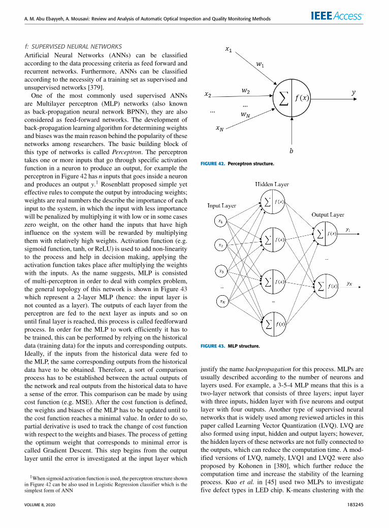
A. M. Abu Ebayyeh, A. Mousavi: Review and Analysis of Automatic Optical Inspection and Quality Monitoring Methods
f: SUPERVISED NEURAL NETWORKSArtificial Neural Networks (ANNs) can be classifiedaccording to the data processing criteria as feed forward andrecurrent networks. Furthermore, ANNs can be classifiedaccording to the necessity of a training set as supervised andunsupervised networks [379].
One of the most commonly used supervised ANNsare Multilayer perceptron (MLP) networks (also knownas back-propagation neural network BPNN), they are alsoconsidered as feed-forward networks. The development ofback-propagation learning algorithm for determining weightsand biases was the main reason behind the popularity of thesenetworks among researchers. The basic building block ofthis type of networks is called Perceptron. The perceptrontakes one or more inputs that go through specific activationfunction in a neuron to produce an output, for example theperceptron in Figure 42 has n inputs that goes inside a neuronand produces an output y.1 Rosenblatt proposed simple yeteffective rules to compute the output by introducing weights;weights are real numbers the describe the importance of eachinput to the system, in which the input with less importancewill be penalized by multiplying it with low or in some caseszero weight, on the other hand the inputs that have highinfluence on the system will be rewarded by multiplyingthem with relatively high weights. Activation function (e.g.sigmoid function, tanh, or ReLU) is used to add non-linearityto the process and help in decision making, applying theactivation function takes place after multiplying the weightswith the inputs. As the name suggests, MLP is consistedof multi-perceptron in order to deal with complex problem,the general topology of this network is shown in Figure 43which represent a 2-layer MLP (hence: the input layer isnot counted as a layer). The outputs of each layer from theperceptron are fed to the next layer as inputs and so onuntil final layer is reached, this process is called feedforwardprocess. In order for the MLP to work efficiently it has tobe trained, this can be performed by relying on the historicaldata (training data) for the inputs and corresponding outputs.Ideally, if the inputs from the historical data were fed tothe MLP, the same corresponding outputs from the historicaldata have to be obtained. Therefore, a sort of comparisonprocess has to be established between the actual outputs ofthe network and real outputs from the historical data to havea sense of the error. This comparison can be made by usingcost function (e.g. MSE). After the cost function is defined,the weights and biases of the MLP has to be updated until tothe cost function reaches a minimal value. In order to do so,partial derivative is used to track the change of cost functionwith respect to the weights and biases. The process of gettingthe optimum weight that corresponds to minimal error iscalled Gradient Descent. This step begins from the outputlayer until the error is investigated at the input layer which
1When sigmoid activation function is used, the perceptron structure shownin Figure 42 can be also used in Logistic Regression classifier which is thesimplest form of ANN
FIGURE 42. Perceptron structure.
FIGURE 43. MLP structure.
justify the name backpropagation for this process. MLPs areusually described according to the number of neurons andlayers used. For example, a 3-5-4 MLP means that this is atwo-layer network that consists of three layers; input layerwith three inputs, hidden layer with five neurons and outputlayer with four outputs. Another type of supervised neuralnetworks that is widely used among reviewed articles in thispaper called Learning Vector Quantization (LVQ). LVQ arealso formed using input, hidden and output layers; however,the hidden layers of these networks are not fully connected tothe outputs, which can reduce the computation time. A mod-ified versions of LVQ, namely, LVQ1 and LVQ2 were alsoproposed by Kohonen in [380], which further reduce thecomputation time and increase the stability of the learningprocess. Kuo et al. in [45] used two MLPs to investigatefive defect types in LED chip. K-means clustering with the
VOLUME 8, 2020 183245
A. M. Abu Ebayyeh, A. Mousavi: Review and Analysis of Automatic Optical Inspection and Quality Monitoring Methods
aid of NCC was first used to divide the area of the chipinto three regions: pad area, luminous zone, and background.The reason behind this step is to classify the defected fea-tures according the region. Otsu auto-thresholding methodwere then used to highlight four features for each selectedregion and the overall chip; these features are area, perimeter,tightness, and defect rate. The extracted features were thenfed to the first MLP that is responsible to decide whetherthe sample contain fragment chip defect are not. Another15-10-5 MLP were used to classify the samples accordingto the remaining four defect types considered. The totalpercentage of defect recognition according to this methodwas 97.83%. Chiou et al. in [203] used two MLPs as well intheir study to investigate the defect occur in the gold-platedregions of BGAs. The first MLP (3-5-2) was used beforethe feature extraction process take place to identify thegold-plated pixels from other pixels. Three inputs were usedto feed this MLP which are R, G and B information foreach pixel. The output layer has two output units, i.e., gold-plating pixel and non-gold-plating pixel. The second MLP(6-7-5-7-4) was used after the features are extracted. Sixinputs were used in this network that represent the num-ber of features extracted, and four outputs that representthe number of defect types considered. The proposed studyachieved good classification accuracy results of 96%. How-ever, it fails to distinguish a defect that is connected tothe non-gold-plating regions, because the pixels that makeup the defect have been classified as non-gold-plating pix-els. Furthermore, the regions inspected, and the number ofdefects considered in this study are limited. Lin in [36] usedtwo approaches to classify water-drop defects on LED chipsurfaces: wavelet-based multivariate statistical (WMS) andMLP network called wavelet-based neural-network (WNN).In WMS, wavelet features were used to obtain the HotellingT 2 value such that the distance between defective featurescan be estimated. The T 2 value is then classified according toupper and lower limits, such that if not in the range this meansa defect has been detected. WNN approach uses four waveletcharacteristics as the input values of MLP neural networkwhich has two neuron outputs that represent two classes:in-control and out-of-control. The detection rates usingWMSand WNN approaches were 92% and 95% with false alarmrates of 5.8% and 7.5% respectively. However, these resultswere contradicted by another study conducted by the sameauthor in [51] that used the same exact approach with differ-ent results obtained. The detection rates for this study usingWMS and WNN approaches were 92.4% and 90.8% withfalse alarm rates of 6.1% and 4.4% respectively. The reasonfor this contradiction is not explicit; however, since the majordifference was in theWNN results, it could be due to differentsample images used in both studies for the training process.In a similar approach, Chiu and Lin in [245] investigatedblemish defects in LCD panels using T 2 hotelling approachwith the aid of ACO and BPNN. The T 2 hotelling valuewere obtained using four color models, so that the distancerepresents the color variations (dark and bright variations
in the grayscale). ACO algorithm is applied to detect theabnormal spot blemishes in the distance diagram. Finally,the BPNN were applied to classify the regions of slight colorvariation blemishes based on the T 2 distance values. Su et al.in [111] used three types of ANNs to inspect semiconductorwafer post-sawing quality, which are BPNN, RBF and LVQ.Where the RBF network can be considered similar to BPNN;however, it only consists of one hidden layer and it lack ofconnection weights between input layer and hidden layer.They achieved optimum results in their study upon using360 image mask size and 224 input nodes for all the neuralnetwork used. The number of hidden layer nodes in the threeANNs to achieve optimum results were; 20 in BPNN withaccuracy of 100%, 15 in RBF with accuracy of 90% and 18 inLVQ with accuracy of 100%. It is clear in this study thatBPNN and LVQ showed an outperformance in the inspectionwhen compared to RBF. However, the proposed study is notsuitable for high variety of defects. In the study conducted byAghaeizadeh Zoroofi et al. in [119], BPNN have also showedan outperformance in classifying IC wafer contaminationdefects when compared to maximum likelihood and max-imum distance classifiers. However, these algorithms wereused as binary classifiers and did not give many detailsabout the defect. Chen et al. in [264] used multiple ANNsto classify TFT-LCD defects during the lithography process.RBF, BPNN, LVQ1 and LVQ2 ANNs have been used andcomparison between their results were investigated. Due tothe difficulty in collecting sufficient defect data, this studysimulated various defect data to fit enough numbers for mod-elling. Special considerations regarding using masks for thesample images have been made, such that the ROI does nottake many inputs from the neural network and in the sametime make it big enough so that the accuracy is not affected.Experimental results showed that LVQ2 had the best accuracyresults with an accuracy of 97%, while RBF performed theworst with an accuracy of 87%. Despite the good results theyhave achieved, the proposed approach is inferior in terms ofsystem setup lead-time and flexibility to product complexity.Sun et al. in [293] have also compared between the per-formance of MLP and LVQ networks to classify four typesof thermal fuses defects. Four features were first extractedusing thresholding, segmentation, and morphological oper-ations, which are mean grayscale value, variance, rang andentropy. These features were used as inputs for both networks.Experimental results have shown an outperformance of MLPover LVQ in terms of accuracy. However, LVQ consumedless computational time compared with MLP. Acciani et al.in [143] proposed two neural networks: LVQ and MLP toclassify five types of solder joint defects. They have alsoconducted experiments on k-NN classifier and compared theperformance between the three classifiers considered. Theinput for these classifiers was the feature vector that containthe geometric and wavelet features of the inspected area, andthe output consisted of five neurons in the ANN classifiers.The results have proved that MLP classifier that fed with thecombined geometric and wavelet feature vector performed
183246 VOLUME 8, 2020
A. M. Abu Ebayyeh, A. Mousavi: Review and Analysis of Automatic Optical Inspection and Quality Monitoring Methods
the best compared with LVQ and k-NN classifiers with arecognition accuracy of 98.8%. However, many limitationshave been noted in this study, such as the number of imagesused to train the classifiers is not the same for all the defecttypes (e.g. 32 images for defect type 5 and 76 images fordefect type 3), this can cause imbalanced data and can affectthe validity of the recognition accuracy obtained. Further-more, the defect types considered in this study was limitedcompared with other similar studies. Another note that theresults obtained in this study were partially contradicted withanother study conducted by the same author in [165], whichobtained 99.5% accuracy for the same approach. However,this contradiction is due to the fact that only a small numberof samples have been tested in the later study. A similarapproach was also proposed by the same authors in [166]in terms of the defects considered and feature extractiontechnique; however, in this study a neuro-fuzzy classifier wasused instead. Their hybrid classifier consisted of three MLPnetworks and two modules based on fuzzy rules. Severaladvantages were observed by using fuzzy-based classifiersuch as low computational costs of the fuzzy systems thatcould satisfy urgent time constraints in the in-line detection.Kuo et al. in [228] used GLCM matrix as inputs to twoANNs: BPNN and RBFNN to classify polarized film defectsinto four types of defects. The accuracy of the classificationprocedure is 98.9% for RBFNN and 97.3% for BPNN and theprocessing time of one single image is 2.57 seconds. Huangin [71] used four self-supervised MLP networks that operatesimultaneously with one hidden layer to detect clustered chipdefects of wafers and classify them to bad and good wafers.The input of the network is fed from the output generated atthe end of preceding training cycle. The feedback connectionbetween the output and input layers were used to elucidatethe structure in the input data without a priori teaching.Backpropagation with gradient descent concept were usedfor the training purposes of the network. Lin in [83] pro-posed BPNN integrated with ACO algorithm to predict thewafer yield. ACO can be integrated with BPNN to look forthe optimal set of parameters (weights and biases), whichcan reduce the time of training process. This will resultin ACO-BPNN. The input for this network is obtained fromthe defect count, cluster index and FVCP. Yang et al. in[214] proposed aBPNN to classify the five defects consideredin the TFT array process. The input for this network werethe eleven features extracted using the GLCM process, andthe output were the five classes considered according to thenumber of defects. Thirty hidden layers were consideredalong with bipolar sigmoid activation function. The defectrecognition rate of proposed system was estimated to be83.3%. However, it is noted that when the defect type changesor type of TFT array samples change, the proposed defectclassifier must be retrained in order to adapt to new defectsor sample, which is considered a limitation for the system.Kuo et al. in [272] proposed a Tagushi based BPNN toclassify four types of color filter defects in LCD panels.The combination of Tagushi and BPNN were utilized to
avoid a possible disadvantage of using BPNN alone such thatthe global minimum cannot be obtained if learning cyclesare insufficient. Four feature values were used as an inputto the BPNN. The output consists of four neurons accord-ing to the defect classes considered (fibre, particle, gel andresisting coating). This study achieved an overall recognitionrate of 94%. In a similar study, Kuo et al. in [273] usedBPNN classifier to classify six types of color filter defectsand the results were compared to another classifier typecalled minimum distance classifier (MDC). MDC classifiercalculates the distance between the unknown graphic typeand all training types and selects the shortest distance fordecision making. The five key features obtained from thefeature extraction step were used as inputs to both classifiers,and the output was the six defect types considered. In thisstudy BPNN achieved an accuracy of 93.7%, while MDCachieved 96.8%. Despite of the good results achieved; theproposed method could not recognize defects in the caseof overlapping of different defects in the same position.Li et al. [221] proposed anMLP with four inputs: width, ratioof fringe, curvature of fringe and fringe size to classify theMura defects into three types. The number of outputs of theMLP were four including the three defect types consideredand the normal (non-defected) case. Ko and Cho in [164]proposed a combined approach of LVQ networks and fuzzyrules to inspect solder joint defects in PCBs. Each inspectedimage is divided into three sub-images and an LVQnetwork isused for each sub-image. The objective of this approach is toreduce the burden of the LVQ classifier when classifying thecomplex solder joint patterns. The input data of each classifierare the color intensities of each pattern as shown in the formof three-color patterns obtained under the three-color circu-lar illumination. To avoid any misclassification, fuzzy logicscheme was integrated with the LVQ classifier. The classi-fication rule is described in a linguistic way like a human’s,rather than represented by precisely numerical quantities andthe classification task is performed by predefined rules. Sev-eral advantages have been observed by using the proposedtechniques: one is that the combination of three discrimi-nant boundary functions makes more complex boundariesthan the original LVQ algorithms. The other is that expertknowledge can be reflected in the pre- defined fuzzy classi-fication rule. Therefore, the classification boundaries can beeasily readjusted, by changing the fuzzy rule tables and mem-bership functions. However, since the proposed approachuses multiple algorithms and deals with three sub-mages foreach image, this can increase the computational time makingthis method not suitable for rapid inspection applications.Ong et al. in [169] proposed LVQ network to classify sol-der joint defects. The input for the classifier were directlyobtained from the grayscale acquired images without fea-ture extraction or preprocessing steps since special cam-era setups were established to avoid these steps as shownin Figure 26. They compared the recognition rate for the clas-sifier according to the images acquired from different setups.They have shown that their classifier performed the best
VOLUME 8, 2020 183247
A. M. Abu Ebayyeh, A. Mousavi: Review and Analysis of Automatic Optical Inspection and Quality Monitoring Methods
when a combination of oblique and orthogonal setups wasused to acquire the images compared with only orthogonalsetup was used. However, when the sample images increaseto about 130 images for training, both setups performedthe same. Their classifier achieved a high recognition rate(up to 100%) with no false alarm. However, their methodhas faced various drawbacks. First, their system is very sen-sitive to lightning variations, therefore the success of a visioninspection system is very much dependent on the good designand robustness of the light source system. Furthermore,despite that feeding the LVQ without preprocessing or fea-ture extraction can reduce a lot from the computational timerequired; however, these steps are still necessary to alleviatethe effects of error arising from different sources of variation.Adly et al. in [57] proposed a novel algorithm that combines ageneral regression network-based (GRN) consensus learningmodel with randomization technique to detect defective pat-terns in semiconductor wafers, where the combination resultsin randomized general regression network (RGRN). GRNare single-pass associative memory feed-forward type ANNswhich use normalized Gaussian kernels in the hidden layeras activation functions [381]. The randomization techniquewas applied by implementing randomized bootstrap to theoriginal data. Randomized bootstrap technique creates ran-dom new subset of data by sampling from the original dataset(with replacement). This method of applying RGRN withrandomization technique were compared to other techniquessuch as MLP and it showed an outperformance compared tothem with an average accuracy of 99.8%. Adly et al. in [88]conducted the same previous approach; however, they pro-posed a data reduction technique based on data partitioningand clustering to simplify the overall algorithm. Voronoi Dia-gram were used for the portioning of data, where it clustersthe whole vector space into smaller Voronoi regions. k-meansclustering is used to fetch the centroid of each Voronoi regionto be used as representative of all original vectors. By usingthe centroids, the size of the data is reduced and there-fore the computation time of the algorithm is also reduced.Their overall accuracy using this technique were slightlyimproved compared with the previous method, as they haveachieved an accuracy of 99.884%. RGRN algorithm wereused again in the study conducted by Tello et al. in [108];however, they added a CNN model in order to identify andclassify both single and mixed defect patterns. This studysuggested using a splitter based on information gain conceptto classify single andmixed patterns separately. The proposedapproach achieved overall accuracy of 86.17%. Even thoughthe accuracy achieved were lower than the one conducted byAdly et al.in [57], [88] that used similar methods; however,these two studies considered single defect patterns only anddid not consider mixed defect patters as in this study.
g: UNSUPERVISED NEURAL NETWORKSFor the scope of this review, unsupervised neural networksare mostly used for identifying defect patterns in WMs.Recurrent networks are example of unsupervised learning
networks. They are called recurrent because inputs to theneurons of these networks come from external input, as wellas from the internal neurons, consisting of both feed-forwardand feedback connections between layers and neurons. Hop-field neural network (HNN), Self-organising map (SOM) andadaptive resonance theory network (ART) are all examples ofrecurrent neural networks [382]. HNN can be used as an asso-ciative memory and can also help in optimization problems.Chang et al. in [44] used two HNNs to investigate LED diedefects. The first one was called Contextual HNN and wasused to locate the dies in the sample sub-images. The numberof the input neurons for this networkwere equal to the numberof pixels for the sample sub-image. The network detectingcriteria must satisfy the fact that intensity distribution ofpixels in die region in the sample sub-image must be similarto that of template image. Since the network is used to identifythe die locations, the output neurons of this network forma die map of individual dies. Each neuron node representsthe state of the pixel digitally, such as if the pixel is locatedwithin a die region the neuron state is 1 otherwise it willbe 0. Therefore, the die map represent a binary image thathas the same dimension as sample sub-images. The regionsthat represent a die location are considered 1’s, and the onesthat are not considered regions are considered 0’s. The dieregion are then identified using CCL algorithm. The secondHNN is called competitive HNN were used to classify thedie image into three classes; light emitting region, p-electrodeand background in an unsupervised approach. The number ofneurons of this network depends on the gray intensity valuesand the number of classes. In competitive HNN, winner takeall (WTA) approach were applied. The WTA ensure that notwo neurons are categorized with two different classes andalso guarantees that all gray scales are classified. The diedefect inspection algorithm were then applied to comparegeometrical and heuristical defects against the selected tem-plate. 10% thresholdmargin were used to compare the samplesub-images with the template image. The method achievedan accuracy of 95% in detecting defective dies. Chen andLiu in [64] used a modified ART called ART1 to recognizepattern wafer defects. Unlike other types of ANNs that areless likely to learn new information without damaging whatwas previously learnt, ART network has the advantage of notforgetting after learning [379]. ART1 is considered an unsu-pervised binary network that accepts binary inputs. In thisstudy, an unsupervised technique were selected as they foundit difficult to decide how many clusters of defect spatial pat-tern to be selected, therefore the learning was accomplishedusing input data alone. They also gave detailed explanationbehind the reason of choosing this algorithm as:• If the characteristic of a new pattern is quite similarto a previously stored pattern (vigilance test passed),only a slight modification of the knowledge containedin the old patterns will be executed. The characteristicsof the old and new patterns can be satisfied and theold knowledge can be properly retained. Stability of thesystem can be maintained.
183248 VOLUME 8, 2020
A. M. Abu Ebayyeh, A. Mousavi: Review and Analysis of Automatic Optical Inspection and Quality Monitoring Methods
• If the characteristics of a new pattern are not similar to allof the previously stored patterns (vigilance test failed),new knowledge for the new pattern will be created. Thisimplies quick learning of a new pattern, or the so-calledplasticity.
The network was able to recognize both ring and scratchdefects using matching values. They compared the perfor-mance of ART1 to SOM. They showed that ART1 outper-formed SOM in the comparison. Even though, they did notachieve high matching scores for the detected pattern; how-ever, this study over comes others in predicting the possi-ble defect patterns rather than assuming a pre-defined sce-nario. Unlike the outcomes achieved in the previous study,Di Palma et al. in [66] showed that ART1 is not adequatedue to AND logic usage, whereas SOM provide completelysatisfactory results including visually effective representationof spatial failure probability of the pattern classes. However,their method cannot separate ring patterns from the othertypes of defect clusters [86]. Liu et al. in [65] implementedthe same approach in [64], in which they used ART1 todetect the defect patterns in WBM. They were able to detectmore patterns than the previous study such as bull’s eyepattern and they reached a recognition rate of 95%. How-ever, the low number of WBM provided to them limitedtheir ability to identify further patterns. Choi et al. in [85]conducted a study similar to what have been done in [64],[65]. However, they proposed an advanced ART1 algorithmcalled ‘‘multi-step ART1’’, where it sequentially uses themodules to classify each pattern separately, instead of trainingall patterns at once. This algorithm has a specific learningprocedure according to the characteristics of each patternby changing and re-learning the preprocessing of the inputdata, the threshold decision method, the type of similarityand the vigilance parameter during module generation. Theirproposed algorithmwas able to detectmore type of defect pat-tern including mixed pattern compared to the similar studies.Hsu and Chien in [58] developed a hybrid data miningapproach which combined ART1 and spatial statistics toquickly extract systematic and random patterns from WBM.Furthermore, a decision tree algorithm was constructed foridentifying the root causes of specific patterns. However,due to the vigilance parameter settings used in ART1, somesystematic patters were misclassified as random patterns inthis study. Hence, the lower the vigilance threshold value,the more patterns are extracted from the maps. On the otherhand, a low vigilance threshold value may also cause dis-similar maps to group in the same cluster. Huang et al.in [72] conducted similar study to what have been investi-gated in [71]. However, cellular neural networks combinedwith genetic algorithm were used to classify wafer patternsinstead. A cellular neural network (not to be confused withconvolutional neural network) is an unsupervised neural net-work that is composed of a massive aggregate of analogcircuit components called cells. Setting up a cellular neuralnetwork needs a proper selection of circuit parameters ofcells. The dynamics of a cellular neural network is determined
by the set of circuit parameters, which are collectively calledthe cloning template. A genetic algorithm was used to settlethe cloning template for the cellular neural network owingto its success in the applications of optimization. This studyoutperformed the previous study in [71] remarkably as itachieved an accuracy of 99.2%. However, the false alarmrate of this study was relatively high. Furthermore, no expla-nation was provided for the different accuracy results forusing MLP algorithm, despite of using same approaches inboth studies. Liu and Chien in [87] used different type ofANNs for different purposes to analyse and classify WBMdefects. Cellular neural network was used first to eliminateWBM defect noise and enhance the patterns against ran-dom errors. Moment invariant and ART1 were then usedfor pattern clustering and classification respectively, wheremoment invariant can make the same shape in one cluster,whether the shape’s size or position are changed. ART1 canself-lern by characteristic of each WBM. These algorithmswere integrated with a user interface system that allows usersto execute the following system operations including: loadingthe analysed dataset, adding or retracting the decision knowl-edge, controlling the parameters in WBM patterns clusteringsystem, and monitoring the clustering results. Chien et al.in [86] used ART1 classifier as a final classification step todeal with the wafer being classified as having spatial randomdefects with higher failure percentage and to find new defectpatterns for further classification. The filtered wafer defectsthat feed ART1 algorithm came from predefined conditionsusing SPC charts that cannot detect all types of defects (e.g.sparse defects). In SPC chart a set of thresholds were usedupper control limit (UCL) and lower control limit (LCL)such that if the failure percentage of the WBM exceeds theUCL the wafer will be classified as a defect, otherwise ifit fall below the LCL will be checked for further defectsusing various filters and ART1 classifier as mentioned before.Chang et al. in [113] proposed an automatic inspectionapproach for classifying wafer defects into four classes basedon a SOM. The feature vector containing GLCM param-eter and color information were used as an input to thenetwork. The inspection results achieved a sensitivity valueof 0.967 and a specificity value of 1.
Unfortunately, unsupervised neural networks involvingSOM, ART, and Cellular Neural Networks cannot identifytwo shift-variant or two rotation-variant defect patterns thatin fact belong to the same failure cause (i.e. distinguishingbetween two parallel scratches or between a top zone and abottom zone) [70].
D. DEEP LEARNINGDeep learning has recently become the most influentialtechnology in machine vision and pattern recognition prob-lems [383]. Deep learning concept involves the usage of DeepNeural Networks (DNN), which can handle feature extractionand classification methods in machine vision problems. DNNis considered a class of ANN; however, the main differencethat make any ANN considered a DNN is DNN consists of
VOLUME 8, 2020 183249

A. M. Abu Ebayyeh, A. Mousavi: Review and Analysis of Automatic Optical Inspection and Quality Monitoring Methods
three hidden layers or more. Moreover, DNN requires littlepreprocessing and feature extraction as these processes areembedded inside the network itself. DNN also uses largenumber of layers compared to the number of nodes to realizehighly nonlinear functions. DNNs learn new useful represen-tations from available features that capture essential statisticalregularities present from data itself, then the representationfeatures can be formulated for classification, regression andspecific problem in information retrieval. The independencefrom prior knowledge and human effort in feature design isa major advantage for deep learning in general and DNNs[384]. For AOI applications reviewed in this paper DNNs areimplemented using the followingmethods: Autoencoders andConvolutional Neural Networks (CNNs).
In DNN, set of models is used to learn high-level abstrac-tions representation in data such as autoencoder (AE), denois-ing autoencoder (DAE) and stacked denoising autoencoder(SDAE) [93]. AE is a three-layer network including encoderand decoder. The encoder maps the input data from ahigh-dimensional space into codes in a low-dimensionalspace, and the decoder reconstructs the inputs from the cor-responding codes. AE can learn features in unsupervisedmanner by minimising reconstructed errors between inputdata and output. However, the intrinsic problems of AE, suchas simply copying input layer to hidden layer, make it noteffective to extract meaningful features even though its outputcan be a perfect recovery of the input data [385]. On the otherhand, DAE takes a corrupted version of data as input andis trained to reconstruct or denoise the original inputs froma corrupted one, which can prevent the AE from just sim-ply learning an identity mapping between the input and thereconstructed output, and captures more informative hiddenpatterns and obtains robust and powerful representations fromthe noisy features. DAE also consists of an encoder processand a decoder process. Several DAEs can be stacked togetherto form a deep network and learn high-level representationswhich can be called SDAE. Therefore, SDAE is considereda special class of DAE where stochastic noise is added to theinput layer of the AE and then trains it to output the sameinput without noise. In general, the training process of SDAEincludes an unsupervised pre-training step and a supervisedfine-tune step. Another popular type of AE family is SparseAutoencoder (SAE) which is considered is a variation ofAutoencoders, where it offers reduction in the neurons used inthe hidden layer and therefore these neurons are consideredinactive and do not fire. This can improve the performanceof traditional autoencoder and exhibits more practical appli-cation values [384], [386]. Hence, autoencoders in generaldo not have the ability to classify on their own and areusually integrated with other deep learning layers such asCNN to fulfill the purpose of classification [387]. Yu in [93]proposed detection and recognition system for detectingWMdefects based on amodified version of SDAE called enhancedstacked denoising autoencoder (ESDAE). They have alsointegrated manifold regularization in the learning procedurewhich improve the algorithm’s performance effectively due
to the preservation of intrinsic information in the data. Theoverall detection accuracy of the proposed method reached89.6% which overcame other methods used for compari-son such that SDAE, DBN, BPN and LR. However, dueto the large number of parameters used, deep autoencodersin general are easy to suffer from overfitting with smallsize sample, which limits the generalization ability of thedeep autoencoders to learn effective features [388]. A similarapproach was also proposed by Lee et al. in [389] to assesswafer’s quality. However, sensor data were used instead ofWM, which is beyond the scope of this review. In a similarstudy that proposed detection and recognition system fordetecting WM defects, Yu et al. in [91] integrated SDAEand CNN to form a new deep learning model called stackedconvolutional sparse denoising auto-encoder SCSDAE.The new model proposed can learn effective features andaccumulate the robustness layer by layer, which adoptsSDAE as the feature extractor and stacks well- designedfully connected SDAE in a convolutional way to obtainmuch robust feature representations. The challenges facedthis study and others that use same dataset is the imbalanceof data, in order to handle this problem under-sampling andover-sampling methods are generally used to against highlyimbalanced datasets. Under-sampling randomly eliminatesmajority class examples, while over-sampling increases thenumber of instances in the minority class. Both of them aimto obtain approximately the same number of instances of theclasses. The detection accuracy rate in this study was 95.13%in the simulation case and 94.75% in the industrial case.The results were compared to other classification algorithmssuch SDAE, AlexNet, DBN, SVM, BPN, k-NN and C4.5 andoutperformed all of them in the simulation and industrialcases. However, the problem of limited training data willlead to overfitting of SCSDAE.Moreover, due to labeled datascarcity for some patterns in WMs, it is a challenging issuefor SCSDAE to implement pattern recognition on imbalanceddataset.
Data imbalance and the lack of training data are majorproblems as mentioned earlier in our discussion. Tradi-tional image augmentation techniques such as rotation, mir-roring and scaling can overcome these problems in somecases. However, as these techniques only manipulate the realdataset without providing new insight for the data, inac-curacy and overfitting in classification results may occur.Goodfellow et al. in [390] proposed GAN that can be usedfor data augmentation to generate more data for training. Theoriginal proposed model consisted of two networks, namely,generator and a discriminator. The two networks are trained atthe same time and compete against each other in a minimaxgame. The generator is trained to deceive the discriminatorby synthesizing realistic samples, whereas the discriminatoris trained to be equipped with high discriminative capabilityfor the synthetic samples. These networks complement eachother and can help to understand the original data distribution,providing a new perspective for the forthcoming classifica-tion algorithm. However, the training of the two networks
183250 VOLUME 8, 2020
A. M. Abu Ebayyeh, A. Mousavi: Review and Analysis of Automatic Optical Inspection and Quality Monitoring Methods
can be quite unstable and may suffer mode collapse prob-lem [391], [392]. Wang et al. in [94] proposed an improvedGAN model integrated with CNN and other deep learningmodels called adaptive balancing generative adversarial net-work (AdaBalGAN) for identification of defective patterns inWMs. This algorithm was specially proposed to enhance theclassification results against imbalanced datasets. Moreover,the study proposed a conditional categorical generative adver-sarial network to rebalance the WM dataset by generatingsimulated instances for minority class of defective patterns.Three parts are involved in the previous process; the firstpart is a pattern recognition model which consists of CNNthat classifies the real WM samples, the second part is agenerative model which also consists of CNN that generatessimulated WMs according to the real samples from first part.Finally, in the last part, a classical CNN (Le-net5) is usedto compare between the real wafer and simulated WMs andguarantee the similarity between them. The proposed methodresulted in high classification accuracy for some patterns(up to 100%) and also outperformed other algorithms thatwere compared to it such as SVM, Adaboost, CNN andGAN. Kim et al. in [255] proposed an algorithm based onCNN with stacking ensemble model and MLP, to classifyfour types of TFT-LCD defects. In their investigation, theyhave noticed that the size of defects is very small comparedto the patterned panel in the background. Therefore, theyproposed a feature extraction scheme to eliminate the patternsin the background for better classification results by applyingthree steps: find the pitch of each panel image, calculate thepitchwise difference score for each pixel and apply thresh-olding. An algorithm was proposed in this study to checkthe efficiency of using the pattern elimination technique byusing several MLP and CNN models. They have achieved anoverall accuracy in their classification of 86.13%. However,they did not mention the time needed for the algorithm as theyused too many models which may affect the computationaltime. Mei et al. in [215] proposed a method that combinedhandcrafted features and unsupervised deep learning-basedfeatures to detect Mura defects in TFT-LCD. The methodwas named joint-feature-representation-based defect recogni-tion framework (JFR-DRF). Various unsupervised algorithmswere compatible for the unsupervised deep learning-basedfeature extraction part; however, SAE algorithm was usedto demonstrate its ability. The handcrafted features wereextracted with methods similar to GLCM technique thatrequires coefficients such as entropy and anisotropy coeffi-cients based on the grayscale histogram. Then, the featuresextracted by these parts will be merged into a single featurevector, which acts as the representation for the Mura defectimage. After subsequent processing, it will be classified usingone-against-all SVM classifier. In this study, it was provenfrom statistical results that combining handcrafted and unsu-pervised feature extraction outperformed the performance ofusing only one of them. However, fused feature represen-tations may also have the risk of being affected by poorrepresentations frommodalities which are not appropriate for
the tasks.Moreover, deep learning-basedmethods can requireconsiderable computational resources and time to performtraining and inferencing [244].Mei et al. in [250] proposed analgorithm to detect texture surface defects in general such asLCD panels, ceramic tiles, and textiles. Where Mura defectsis one of the LCD panel defects investigated in this paper. Thealgorithm is carried out by reconstructing image patches withmultiscale convolutional DAE (MSCDAE). The MSCDAEmethod employs a three-layer pyramid to perform multiscaledefect inspection. This study used only defective-free sam-ples for model training, since collecting and labelling largenumber of defective samples is cumbersome. However, theirapproach requires a separate model to be trained and testedfor each layer; therefore, it is time-consuming and leads toexcessive memory consumption. Their approach achieveda reasonable recall but relatively low precision [256].Yang et al. in [256] overcame the limitation in the previousstudy and proposed an algorithm based on fully convolutionalautoencoder approach (MS-FCAE) to inspect texture sur-face defects including TFT-LCD defects. This algorithm canaccurately segment various types of product surface defectsbased on a small number of defect-free product samples(50 defect-free sample). The data sample for the TFT-LCDdefects includes spot defects, line defects, and region defects.Their inspection results showed that the proposed algorithmboth simultaneously and accurately inspects all types ofTFT-LCD defects as it achieved a 98.1% recall and 92.1%precision, whereas the other defect inspection methods com-pared with the proposed are suitable only for certain typesof defects. Furthermore, compared with MSCDAE usedin [250], MS-FCAE requires no redundant computation at all.Jo and Kim in [286] proposed a regularized auto-encoderalgorithm as a features extraction approach to separatethe background of images from the defective regions forinspecting displays of mobile devices. This study focused oncomparing their approach to similar feature extraction anddimension reduction approaches low-rank-approximation-based separation methods (specifically SVD) and thesegmentation-based method. They have shown that their pro-posed method was able to detect defects ranging from highvisibility such as faint dot type defects to not clearly visiblebecause of the small intensity difference from the backgroundsuch as Mura defects. On the other hand, the previously men-tioned approaches failed to detect these defects. Despite thatSVD outperformed the proposed method in terms of the com-putation timewith an average 183ms comparedwith 313ms inthe proposed method. Many drawbacks were also observed inthis study, such as in the simulated defect images, overlappingdefects were not considered. Furthermore, the method needsto repeat inspection several parts of an image ofmobile devicebecause it only processes 700 × 990 size image due to thelimitation of computing resources.
A special case of DNNs is when the matrix multipli-cations include convolutional filter operations, which iscommon in DNNs that are designed for image and videoanalysis. Such models are known as convolutional neural
VOLUME 8, 2020 183251
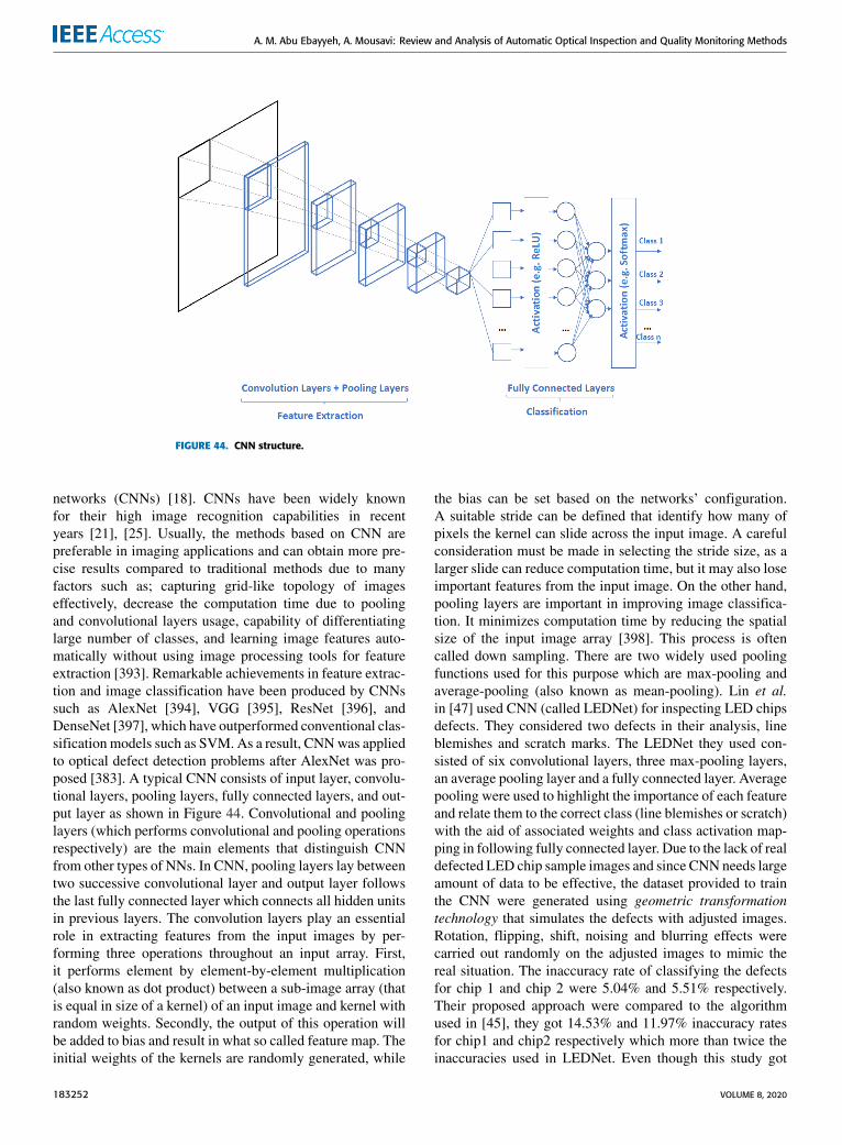
A. M. Abu Ebayyeh, A. Mousavi: Review and Analysis of Automatic Optical Inspection and Quality Monitoring Methods
FIGURE 44. CNN structure.
networks (CNNs) [18]. CNNs have been widely knownfor their high image recognition capabilities in recentyears [21], [25]. Usually, the methods based on CNN arepreferable in imaging applications and can obtain more pre-cise results compared to traditional methods due to manyfactors such as; capturing grid-like topology of imageseffectively, decrease the computation time due to poolingand convolutional layers usage, capability of differentiatinglarge number of classes, and learning image features auto-matically without using image processing tools for featureextraction [393]. Remarkable achievements in feature extrac-tion and image classification have been produced by CNNssuch as AlexNet [394], VGG [395], ResNet [396], andDenseNet [397], which have outperformed conventional clas-sification models such as SVM. As a result, CNNwas appliedto optical defect detection problems after AlexNet was pro-posed [383]. A typical CNN consists of input layer, convolu-tional layers, pooling layers, fully connected layers, and out-put layer as shown in Figure 44. Convolutional and poolinglayers (which performs convolutional and pooling operationsrespectively) are the main elements that distinguish CNNfrom other types of NNs. In CNN, pooling layers lay betweentwo successive convolutional layer and output layer followsthe last fully connected layer which connects all hidden unitsin previous layers. The convolution layers play an essentialrole in extracting features from the input images by per-forming three operations throughout an input array. First,it performs element by element-by-element multiplication(also known as dot product) between a sub-image array (thatis equal in size of a kernel) of an input image and kernel withrandom weights. Secondly, the output of this operation willbe added to bias and result in what so called feature map. Theinitial weights of the kernels are randomly generated, while
the bias can be set based on the networks’ configuration.A suitable stride can be defined that identify how many ofpixels the kernel can slide across the input image. A carefulconsideration must be made in selecting the stride size, as alarger slide can reduce computation time, but it may also loseimportant features from the input image. On the other hand,pooling layers are important in improving image classifica-tion. It minimizes computation time by reducing the spatialsize of the input image array [398]. This process is oftencalled down sampling. There are two widely used poolingfunctions used for this purpose which are max-pooling andaverage-pooling (also known as mean-pooling). Lin et al.in [47] used CNN (called LEDNet) for inspecting LED chipsdefects. They considered two defects in their analysis, lineblemishes and scratch marks. The LEDNet they used con-sisted of six convolutional layers, three max-pooling layers,an average pooling layer and a fully connected layer. Averagepooling were used to highlight the importance of each featureand relate them to the correct class (line blemishes or scratch)with the aid of associated weights and class activation map-ping in following fully connected layer. Due to the lack of realdefected LED chip sample images and since CNN needs largeamount of data to be effective, the dataset provided to trainthe CNN were generated using geometric transformationtechnology that simulates the defects with adjusted images.Rotation, flipping, shift, noising and blurring effects werecarried out randomly on the adjusted images to mimic thereal situation. The inaccuracy rate of classifying the defectsfor chip 1 and chip 2 were 5.04% and 5.51% respectively.Their proposed approach were compared to the algorithmused in [45], they got 14.53% and 11.97% inaccuracy ratesfor chip1 and chip2 respectively which more than twice theinaccuracies used in LEDNet. Even though this study got
183252 VOLUME 8, 2020
A. M. Abu Ebayyeh, A. Mousavi: Review and Analysis of Automatic Optical Inspection and Quality Monitoring Methods
considerably low inaccuracy results; however, their algorithmwere limited to classify only two kind of defects. Further-more, there was no evidence that their adjusted images forthe training set can simulate the real case for defected chips.Yang et al. in [41] used CNN for the purpose of assessing thediameter of the LED cup aperture. Since no feature extractionneeded to feed the CNN, the images were directly used as theinput neurons of the network. The network consisted of fiveconvolution layers and two fully connected layers. Trainingsamples for the network were used from the captured images,each sample of the image were rotated 90◦ four times andhorizontal flip were applied to each image to further increasethe training samples for the network. The detection rate forunqualified cups was 100%with false alarm rate of 8%. How-ever, the need for a large labelled dataset may limit its applica-tion [399]. For semiconductor wafer inspection, Kyeong andKim in [104] used CNN in their classification, in which theyconsidered the WBM as an input binary matrix of 0s and 1sthat have a size of 56× 53. In their study three convolutionallayers, three pooling layers and a fully connected layer withReLU and softmax activation functions have been used. TheCNN model that they have proposed for classification wasdesigned to detect multiple defects on same wafer. In orderto do so, they proposed four individual CNN classifiers foreach defect class, in such away that each classifier determineswhether the corresponding pattern exists when several defectpatterns are mixed over a wafer. The main drawback of thisapproach is that to detect a mixed pattern defect, the outputof each individual classifier has to be obtained [400]. A sim-ilar approach was proposed by Cheon et al. in [134]. Theproposed CNN model in this study can extract features fromthe real wafer images that are acquired using SEM and accu-rately classify the input data into five different wafer defectclasses. Their model can also classify the unknown defectclasses by combining the CNN model with k-NN classifier.However, the data used in this study were highly imbalancedand no solution were proposed to mitigate the outcomes ofthis issue [401]. Nakazawa and Kulkarni in [106] also usedCNN with three convolutional layers, three pooling layersand two fully connected layers for wafer inspection. Theinput wafer image size was 286× 400. To evaluate the CNNperformance 28,600WBM imageswere generated in additionto 1191 real wafers for 22 defect classes which improved thetest accuracy up to 98.2%. However, there was high relianceon simulated data for training and validation of the CNNmodel because real datawas highly imbalanced. Furthermore,this study does not provide any information about the defectcluster, size and its location. In a later study conducted bythe same authors in [107], Nakazawa and Kulkarni overcamethe lack of information problem using different type of CNNmodels such as Fully Convolutional Network (FCN) [402],SegNet [403] and U-Net [404]. These models were comparedto each other with regards to their classification performanceand training time. The main concept of FCN is to replacethe fully connected layers of typical classification neuralnetworks with convolutional layers so that a network output
can be a two-dimensional heat map, rather than multiple setof classes. In FCN, shallow layer’s outputs are merged todeeper layers so that the network can maintain both local andcoarse information. SegNet were designed to be an efficientarchitecture for pixel wise semantic segmentation, where itconsists of an encoder network, a corresponding decodernetwork followed by a pixel-wise classification layer. Eachof the encoder and decoder networks consist of 13 convo-lutional layers. The decoder uses pooling indices computedin a max pooling step of the corresponding encoder to per-form non-linear up- sampling. Since positional or boundaryinformation are lost during the max pooling operations inthe encoder network, maintaining positional information foreach up-sampling operation in the decoder network is criticalfor accurate pixel-wise segmentation [403]. U-Net is similarto SegNet in terms of having encoder-decoder architecture;however, instead of using the pooling indices in the maxpooling step, U-net copies and crops a feature map in eachencoder layer to the corresponding decoder layer to maintainlocal positional information. For the segmentation problem,maintaining local information is the key so that each architec-ture has its own way to transfer local details from shallowerlayers to deeper layers. SegNet and U-Net models outper-formed FCN in classify WMs with predefined classes andunseen defects. However, they tookmuch longer training timethan FCN. Yu et al. in [92] constructed an algorithm based onCNN to recognize and classify WM defects. The proposedmethod was divided into two parallel approaches: offlinemodelling and online processing. In the offline modellingstage, a wafer defect pattern recognition model that consistedof two sub-models was constructed. These two sub-modelswere basically two CNNs, one of them was responsible forwafer defect pattern detection and the other for wafer defectpattern classification. Both CNNs consisted of three con-volutional layers and three pooling layers, while the detec-tion CNN consisted of two FC layers and the classificationCNN consisted of three FC layers. Dropout method wereused in both CNNs to avoid overfitting. Furthermore, PCAmethod were used in the classification CNN after the secondFC layer to reduce the feature dimension and then featureswere normalized. In the online processing stage, the WMis pre-processed and used as an input to both CNN models.It was noticed in their study that the detection CNN has a sim-ple structure and a fast computing speed compared with theclassification CNN due to low probability of process faultsin the actual manufacturing process. Their proposed methodachieved an average detection accuracy of 93.13%, whichoutperformed the accuracy of other algorithm that were usedfor comparison. However, using PCA for feature reductionis redundant since CNN has the ability of considering theimportant features and discarding the unnecessary ones.
Most of the researchers that investigatedWMdefects usingCNN are using simulated data to solve the problem of noisyand imbalanced data for WM pattern defect identification.In this way, they can improve the classification accuracy, butit becomes costly and time-consuming. Also, denoising the
VOLUME 8, 2020 183253
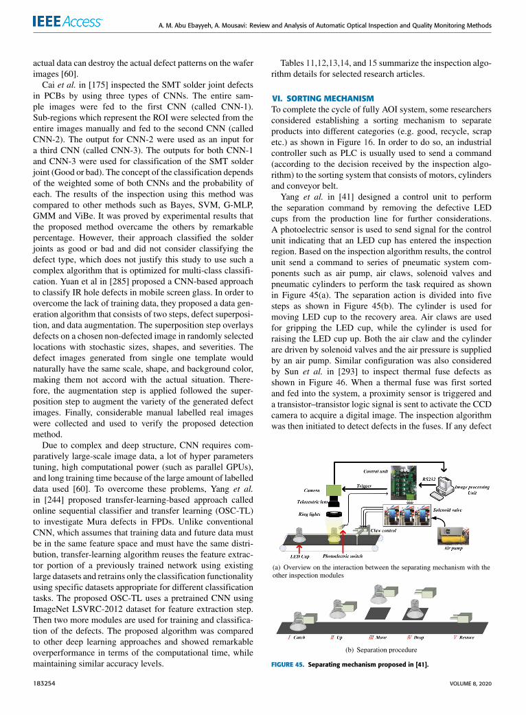
A. M. Abu Ebayyeh, A. Mousavi: Review and Analysis of Automatic Optical Inspection and Quality Monitoring Methods
actual data can destroy the actual defect patterns on the waferimages [60].
Cai et al. in [175] inspected the SMT solder joint defectsin PCBs by using three types of CNNs. The entire sam-ple images were fed to the first CNN (called CNN-1).Sub-regions which represent the ROI were selected from theentire images manually and fed to the second CNN (calledCNN-2). The output for CNN-2 were used as an input fora third CNN (called CNN-3). The outputs for both CNN-1and CNN-3 were used for classification of the SMT solderjoint (Good or bad). The concept of the classification dependsof the weighted some of both CNNs and the probability ofeach. The results of the inspection using this method wascompared to other methods such as Bayes, SVM, G-MLP,GMM and ViBe. It was proved by experimental results thatthe proposed method overcame the others by remarkablepercentage. However, their approach classified the solderjoints as good or bad and did not consider classifying thedefect type, which does not justify this study to use such acomplex algorithm that is optimized for multi-class classifi-cation. Yuan et al in [285] proposed a CNN-based approachto classify IR hole defects in mobile screen glass. In order toovercome the lack of training data, they proposed a data gen-eration algorithm that consists of two steps, defect superposi-tion, and data augmentation. The superposition step overlaysdefects on a chosen non-defected image in randomly selectedlocations with stochastic sizes, shapes, and severities. Thedefect images generated from single one template wouldnaturally have the same scale, shape, and background color,making them not accord with the actual situation. There-fore, the augmentation step is applied followed the super-position step to augment the variety of the generated defectimages. Finally, considerable manual labelled real imageswere collected and used to verify the proposed detectionmethod.
Due to complex and deep structure, CNN requires com-paratively large-scale image data, a lot of hyper parameterstuning, high computational power (such as parallel GPUs),and long training time because of the large amount of labelleddata used [60]. To overcome these problems, Yang et al.in [244] proposed transfer-learning-based approach calledonline sequential classifier and transfer learning (OSC-TL)to investigate Mura defects in FPDs. Unlike conventionalCNN, which assumes that training data and future data mustbe in the same feature space and must have the same distri-bution, transfer-learning algorithm reuses the feature extrac-tor portion of a previously trained network using existinglarge datasets and retrains only the classification functionalityusing specific datasets appropriate for different classificationtasks. The proposed OSC-TL uses a pretrained CNN usingImageNet LSVRC-2012 dataset for feature extraction step.Then two more modules are used for training and classifica-tion of the defects. The proposed algorithm was comparedto other deep learning approaches and showed remarkableoverperformance in terms of the computational time, whilemaintaining similar accuracy levels.
Tables 11,12,13,14, and 15 summarize the inspection algo-rithm details for selected research articles.
VI. SORTING MECHANISMTo complete the cycle of fully AOI system, some researchersconsidered establishing a sorting mechanism to separateproducts into different categories (e.g. good, recycle, scrapetc.) as shown in Figure 16. In order to do so, an industrialcontroller such as PLC is usually used to send a command(according to the decision received by the inspection algo-rithm) to the sorting system that consists of motors, cylindersand conveyor belt.
Yang et al. in [41] designed a control unit to performthe separation command by removing the defective LEDcups from the production line for further considerations.A photoelectric sensor is used to send signal for the controlunit indicating that an LED cup has entered the inspectionregion. Based on the inspection algorithm results, the controlunit send a command to series of pneumatic system com-ponents such as air pump, air claws, solenoid valves andpneumatic cylinders to perform the task required as shownin Figure 45(a). The separation action is divided into fivesteps as shown in Figure 45(b). The cylinder is used formoving LED cup to the recovery area. Air claws are usedfor gripping the LED cup, while the cylinder is used forraising the LED cup up. Both the air claw and the cylinderare driven by solenoid valves and the air pressure is suppliedby an air pump. Similar configuration was also consideredby Sun et al. in [293] to inspect thermal fuse defects asshown in Figure 46. When a thermal fuse was first sortedand fed into the system, a proximity sensor is triggered anda transistor–transistor logic signal is sent to activate the CCDcamera to acquire a digital image. The inspection algorithmwas then initiated to detect defects in the fuses. If any defect
FIGURE 45. Separating mechanism proposed in [41].
183254 VOLUME 8, 2020
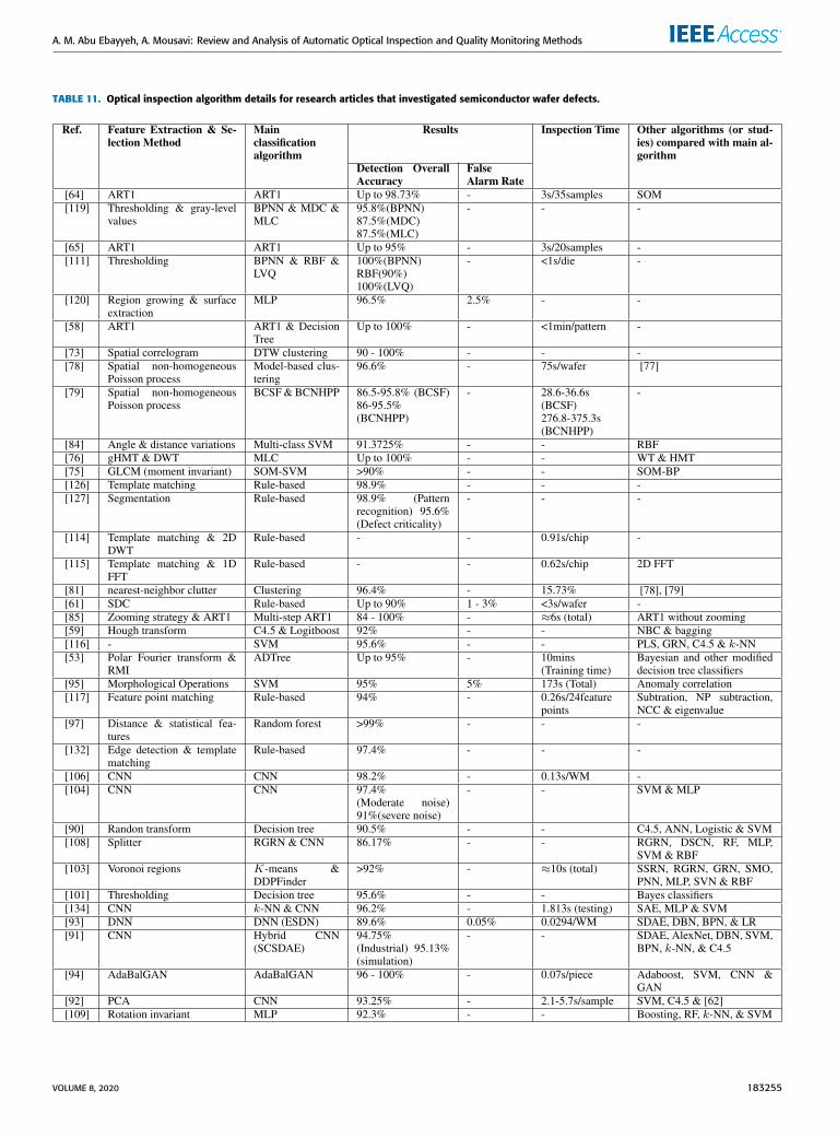
A. M. Abu Ebayyeh, A. Mousavi: Review and Analysis of Automatic Optical Inspection and Quality Monitoring Methods
TABLE 11. Optical inspection algorithm details for research articles that investigated semiconductor wafer defects.
VOLUME 8, 2020 183255
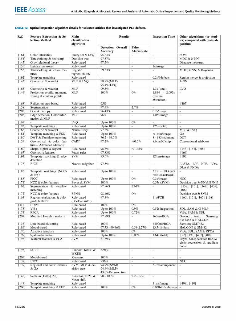
A. M. Abu Ebayyeh, A. Mousavi: Review and Analysis of Automatic Optical Inspection and Quality Monitoring Methods
TABLE 12. Optical inspection algorithm details for selected articles that investigated PCB defects.
183256 VOLUME 8, 2020
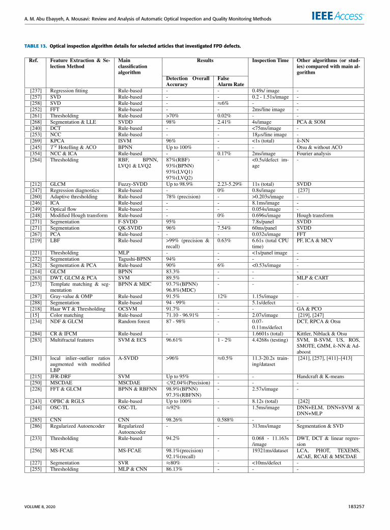
A. M. Abu Ebayyeh, A. Mousavi: Review and Analysis of Automatic Optical Inspection and Quality Monitoring Methods
TABLE 13. Optical inspection algorithm details for selected articles that investigated FPD defects.
VOLUME 8, 2020 183257
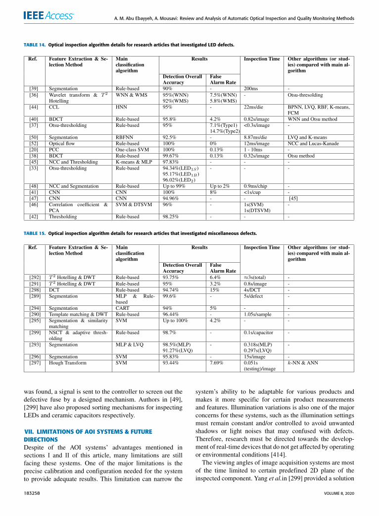
A. M. Abu Ebayyeh, A. Mousavi: Review and Analysis of Automatic Optical Inspection and Quality Monitoring Methods
TABLE 14. Optical inspection algorithm details for research articles that investigated LED defects.
TABLE 15. Optical inspection algorithm details for research articles that investigated miscellaneous defects.
was found, a signal is sent to the controller to screen out thedefective fuse by a designed mechanism. Authors in [49],[299] have also proposed sorting mechanisms for inspectingLEDs and ceramic capacitors respectively.
VII. LIMITATIONS OF AOI SYSTEMS & FUTUREDIRECTIONSDespite of the AOI systems’ advantages mentioned insections I and II of this article, many limitations are stillfacing these systems. One of the major limitations is theprecise calibration and configuration needed for the systemto provide adequate results. This limitation can narrow the
system’s ability to be adaptable for various products andmakes it more specific for certain product measurementsand features. Illumination variations is also one of the majorconcerns for these systems, such as the illumination settingsmust remain constant and/or controlled to avoid unwantedshadows or light noises that may confused with defects.Therefore, research must be directed towards the develop-ment of real-time devices that do not get affected by operatingor environmental conditions [414].
The viewing angles of image acquisition systems are mostof the time limited to certain predefined 2D plane of theinspected component. Yang et al.in [299] provided a solution
183258 VOLUME 8, 2020
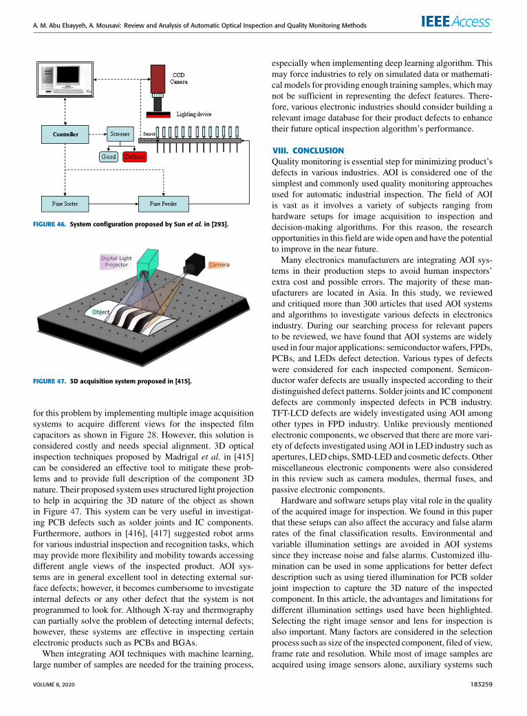
A. M. Abu Ebayyeh, A. Mousavi: Review and Analysis of Automatic Optical Inspection and Quality Monitoring Methods
FIGURE 46. System configuration proposed by Sun et al. in [293].
FIGURE 47. 3D acquisition system proposed in [415].
for this problem by implementing multiple image acquisitionsystems to acquire different views for the inspected filmcapacitors as shown in Figure 28. However, this solution isconsidered costly and needs special alignment. 3D opticalinspection techniques proposed by Madrigal et al. in [415]can be considered an effective tool to mitigate these prob-lems and to provide full description of the component 3Dnature. Their proposed system uses structured light projectionto help in acquiring the 3D nature of the object as shownin Figure 47. This system can be very useful in investigat-ing PCB defects such as solder joints and IC components.Furthermore, authors in [416], [417] suggested robot armsfor various industrial inspection and recognition tasks, whichmay provide more flexibility and mobility towards accessingdifferent angle views of the inspected product. AOI sys-tems are in general excellent tool in detecting external sur-face defects; however, it becomes cumbersome to investigateinternal defects or any other defect that the system is notprogrammed to look for. Although X-ray and thermographycan partially solve the problem of detecting internal defects;however, these systems are effective in inspecting certainelectronic products such as PCBs and BGAs.
When integrating AOI techniques with machine learning,large number of samples are needed for the training process,
especially when implementing deep learning algorithm. Thismay force industries to rely on simulated data or mathemati-cal models for providing enough training samples, whichmaynot be sufficient in representing the defect features. There-fore, various electronic industries should consider building arelevant image database for their product defects to enhancetheir future optical inspection algorithm’s performance.
VIII. CONCLUSIONQuality monitoring is essential step for minimizing product’sdefects in various industries. AOI is considered one of thesimplest and commonly used quality monitoring approachesused for automatic industrial inspection. The field of AOIis vast as it involves a variety of subjects ranging fromhardware setups for image acquisition to inspection anddecision-making algorithms. For this reason, the researchopportunities in this field are wide open and have the potentialto improve in the near future.
Many electronics manufacturers are integrating AOI sys-tems in their production steps to avoid human inspectors’extra cost and possible errors. The majority of these man-ufacturers are located in Asia. In this study, we reviewedand critiqued more than 300 articles that used AOI systemsand algorithms to investigate various defects in electronicsindustry. During our searching process for relevant papersto be reviewed, we have found that AOI systems are widelyused in fourmajor applications: semiconductor wafers, FPDs,PCBs, and LEDs defect detection. Various types of defectswere considered for each inspected component. Semicon-ductor wafer defects are usually inspected according to theirdistinguished defect patterns. Solder joints and IC componentdefects are commonly inspected defects in PCB industry.TFT-LCD defects are widely investigated using AOI amongother types in FPD industry. Unlike previously mentionedelectronic components, we observed that there are more vari-ety of defects investigated using AOI in LED industry such asapertures, LED chips, SMD-LED and cosmetic defects. Othermiscellaneous electronic components were also consideredin this review such as camera modules, thermal fuses, andpassive electronic components.
Hardware and software setups play vital role in the qualityof the acquired image for inspection. We found in this paperthat these setups can also affect the accuracy and false alarmrates of the final classification results. Environmental andvariable illumination settings are avoided in AOI systemssince they increase noise and false alarms. Customized illu-mination can be used in some applications for better defectdescription such as using tiered illumination for PCB solderjoint inspection to capture the 3D nature of the inspectedcomponent. In this article, the advantages and limitations fordifferent illumination settings used have been highlighted.Selecting the right image sensor and lens for inspection isalso important. Many factors are considered in the selectionprocess such as size of the inspected component, filed of view,frame rate and resolution. While most of image samples areacquired using image sensors alone, auxiliary systems such
VOLUME 8, 2020 183259
A. M. Abu Ebayyeh, A. Mousavi: Review and Analysis of Automatic Optical Inspection and Quality Monitoring Methods
as OCT and SEM have been also used to aid the process.Thermography and X-ray can be also used to acquire sampleimages for certain applications such as in PCB and BGAinspection. Circuit probe inspection is widely used to investi-gate semiconductor wafer defects such that WM images canbe generated for defect classification.
Inspection algorithms that process the acquired imageswere also introduced. Three main stages are used in applyingthe inspection algorithm: preprocessing, feature extraction &selection and classification. In preprocessing, several filter-ing, denoising and geometrical operations are applied to theacquired image. This is very useful in removing the unwantednoise that affects the classification decision. Denoising isessential step in removing random defects fromWM patternssuch that inspected samples can be classified according tothe systematic defect. In the feature extraction & selection,the algorithm tries to isolate and locate the defective featuresin the image. Several statistical and geometrical measure-ments are also used to assess the features of defect. Seg-mentation and template matching are two well-used featureextraction algorithms according to the reviewed papers. Fea-ture selection process can reduce the number of redundantextracted features such that the algorithm performs muchfaster. PCA is one of the mostly used algorithms for featureselection. Finally, classification is the decision-making stageof inspection algorithm. Rule-based and learning-based aretwo classification approaches used in the reviewed papers.In rule-based, a set of pre-programmed if-then rules areused to assess the features acquired from the previous step.In learning-based classification, supervised and unsupervisedmachine learning algorithms such as k-NN, Bayes, decisiontrees, SVM, clustering and ANNs are used for the classifica-tion process. Unsupervised machine learning algorithms arewidely used in finding WM patters to investigate semicon-ductor wafer defects, while supervised learning techniquesare used in the rest of studies. In general, machine learn-ing algorithms overcome rule-based learning by their abilityto find anomalies in the input data (features) based on thetraining process and without any need of customized pro-gramming. However, overfitting and imbalanced data are twomajor drawbacks in using learning-based algorithm. Thesetwo problems can be solved by having sufficient data for eachdefect class considered or by applying several techniquessuch as regularization and bootstrapping.
Many recent articles have also used deep learning algo-rithms in investigating defects. The recent development ofCNNs such as AlexNet opened the door for these mod-els to be used in AOI tasks. Deep learning models can dopreprocessing, feature extraction & selection and classifica-tion all at once within their hidden layers. In deep learninglayers, many complex features can be captured that tradi-tional feature extraction approaches may fail to recognize.The detection accuracy can be also improved using deeplearning due to the large number of parameters used intraining the models. Despite previously mentioned advan-tages, deep learning models are considered data hungry.
Furthermore, it requires large processing and GPU capabil-ities. The large data required for training are essential inproviding high accuracy and to avoid overfitting. Several dataaugmentation approaches are used to address this issue suchas using GAN. Transfer learning can be used to avoid largememory usage by implementing pretrained deep learningmodels.
AOI systems are still facing some limitations that requirefurther improvements. For instance, they are most of the timelimited for inspecting surface defects. Furthermore, the view-ing angles for the inspected components are usually fixed tocertain angles which may prevent the system to miss someparts. Robot arm and 3D inspection approaches can be usedto mitigate these problems.
The current technologies and algorithms used in thisreview are currently being tested and some of them will beimplemented in EU funded project called IQONIC that usesAOI technologies to investigate optoelectronics defects.
APPENDIXSEARCHING CRITERIA & KEYWORDS SELECTIONThe most logical choice of keywords that is relevant to themain scope of this research would be ‘‘Optical Inspection’’AND ‘‘Electronic component’’. However, researchers tendto use the specific electronic component that they are ana-lyzing for the title and keyword indexing in their researcharticles instead of using general terms such as electronicparts. Therefore, it is not straightforward task to chooseone keyword to follow in this research. In order to over-come this problem, more general keywords were used suchas ‘‘Inspection’’ AND (‘‘Machine Vision’’ OR ‘‘ComputerVision’’). Even though the previous keyword will show manyirrelevant results (the total is around 7000 results); how-ever, it makes it possible to choose the relevant researcharticles manually. It has been found from the previous key-word search that a lot of researchers who studied electron-ics defects focused their attention to printed circuit boardsPCBs, semiconductor wafers, light emitting diodes LEDs, flatpanel displays FPDs, and other miscellaneous componentssuch as passive electronics and camera modules. Accordingto that, the keywords were adjusted to explore more aboutthe most commonly investigated defects. The new keywordsare:
• ‘‘Optical Inspection’’ AND ‘‘LED’’• ‘‘Optical Inspection’’ AND ‘‘Wafer’’• ‘‘Optical Inspection’’ AND ‘‘PCB’’• ‘‘Optical Inspection’’ AND ‘‘FPD’’
Manual searching technique were also conducted by explor-ing the references used in the reviewed papers.
LIST OF ABBREVIATIONSThe acronyms and abbreviations used throughout the reviewand their definitions are listed below:
183260 VOLUME 8, 2020

A. M. Abu Ebayyeh, A. Mousavi: Review and Analysis of Automatic Optical Inspection and Quality Monitoring Methods
A-SVDD Adaptive Support Vector Data DescriptionACO Ant Colony OptimizationADTree Alternating Decision TreeAE AutoencoderANN Artificial Neural NetworkANOVA Analysis of VarianceAOI Automatic Optical InspectionART Adaptive Resonance TheoryAS-PSO Accelerated Particle Swarm OptimizationBDCT Block Discrete Cosine TransformBGA Ball Grid ArrayBPNN Back Propagation Neural NetworkCART Classification and Regression TreeCCD Charge-coupled DeviceCCL Connected Component LabellingCH Contact HoleCMOS Complementary Metal-oxide SemiconductorCMP Chemical Mechanical ProcessCNN Convolutional Neural NetworkCOB Chip-on-boardCR Contour-based RegistrationDAE Denoising AutoencoderDBSCAN Density-based Spatial Clustering of
Applications with NoiseDCT Direct Cosine TransformDDPFinder Dominant Defective Patterns FinderDFT Discrete Fourier TransformDIP Dual-in-line PackageDNN Deep Neural NetworkDRAM Dynamic-random Access MemoryDTSVM Decision Tree Support Vector MachineDTW Dynamic Time WrappingDWT Direct Wavelet TransformECS Example ContributionESDAE Enhanced Stacked Denoising AutoencoderEWMA Exponentially Weighted Moving AverageE–M Expectation–maximizationF-SVDD Fast Support Vector Data DescriptionFCN Fully Connected NetworkFFT Fast Fourier TransformFOV Field of ViewFPD Flat Panel DisplayFR Frame RateFVCP Fuzzy Variable of Clustering PatternGA Genetic AlgorithmGAN Generative Adversarial NetworkGB Gradient BoostingGE Gate ElectrodegHMT Growing Wavelet Hidden Markov TreeGLCM Graylevel Co-occurrence MatrixGRN General Regression NetworkHDR High-dynamic-rangeHNN Hopfield Neural NetworkHP High PowerIC Integrated CircuitICA Independent Component Analysis
IFCM Improved Fuzzy c-means ClusteringINCC Improved Normalized Cross CorrelationIR-CUT Infrared Cut-offk-NN k-Nearest
NeighborKPCA Kernel Principle Component AnalysisLBF Local Binary FittingLBP Local Binary PatternsLCD Liquid Crystal DisplayLCL Lower Control LimitLDIM Localized Defects Image ModelLED Light Emitting DiodeLVQ Learning Vector QuantizationMCV Markov Concurrent VisionMDC Minimum Distance ClassifierMKSVR Multiple Kernel Support Vector RegressionMLP Multi-layer
PerceptronMS-FCAE Fully Convolutional AutoencoderMSCDAE Multiscale Convolutional Denoising
AutoencodeMSE Mean Square ErrorNCC Normalized Cross CorrelationNDF Neighboring Difference FilterNSCT Non-subsampled
Contourlet TransformOCSVM One-class
Support Vector MachineOCT Optical Coherence TomographyOLED Organic Light Emitting DiodeOPBC Outlier prejudging-based Image
Background ConstructionOSC-TL Online Sequential Classifier and Transfer
LearningPC Principle ComponentPCA Principle Component AnalysisPCB Printed Circuit BoardPCC Pearson’s Correlation CoefficientPE Pixel ElectrodePICC Partial Information Correlation CoefficientPLC Programmable Logic ControllerPLED Polymer Light Emitting diodePLS Partial Least SquaresPR Pixel ResolutionPSO Particle Swarm OptimizationQK-SVDD Quasiconformal Kernel Support Vector Data
DescriptionRBF Radial-basis
FunctionRGRN Randomized General Regression NetworkRMI Rotational Moment InvariantsROI Region of InterestRPCA Robust Principle Component AnalysisSAE Sparse AutoencoderSD Source and DrainSDAE Stacked Denoising Autoencoder
VOLUME 8, 2020 183261
A. M. Abu Ebayyeh, A. Mousavi: Review and Analysis of Automatic Optical Inspection and Quality Monitoring Methods
SDC Segmentation, Detection, and Cluster-Extraction
SE Semiconductor ElectrodeSEM Scanning Electron MicroscopeSMD Surface-mounted
DeviceSMOTE Synthetic Minority Over-sampling TechniqueSMT Surface Mount TechnologySOM Self-organising
MapSPC Statistical Process ControlSURF Speeded Up Robust Feature ExtractionSVC Support Vector ClusteringSVD Singular Value DecompositionSVDD Support Vector Data DescriptionSVM Support Vector MachineSVR Support Vector RegressionSZ Sensor SizeTCS Truncated Component SolutionTFT Thin-film
TransistorTHT Through Hole TechnologyUCL Upper Control LimitViBe Visual Background extractionWBM Wafer Bin MapWD Working DistanceWKDE Weighted kernel density estimationWM Wafer MapWMS Wavelet-based
Multivariate StatisticalWNN Wavelet-based
Neural NetworkWTA Winner Take AllWTMS Wavelet Tansform Modulus Sum
REFERENCES[1] J. A. C. Soto, F. Tavakolizadeh, and D. Gyulai, ‘‘An online machine learn-
ing framework for early detection of product failures in an industry 4.0context,’’ Int. J. Comput. Integr. Manuf., vol. 32, nos. 4–5, pp. 452–465,May 2019.
[2] Y. Liu, C. Jiang, and H. Zhao, ‘‘Using contextual features and multi-viewensemble learning in product defect identification from online discussionforums,’’ Decis. Support Syst., vol. 105, pp. 1–12, Jan. 2018.
[3] T. Czimmermann, G. Ciuti, M. Milazzo, M. Chiurazzi, S. Roccella,C. M. Oddo, and P. Dario, ‘‘Visual-based defect detection and classifica-tion approaches for industrial applications—A survey,’’ Sensors, vol. 20,no. 5, pp. 1–25, 2020.
[4] T. D’Orazio, M. Leo, A. Distante, C. Guaragnella, V. Pianese, andG. Cavaccini, ‘‘Automatic ultrasonic inspection for internal defect detec-tion in composite materials,’’ NDT & E Int., vol. 41, no. 2, pp. 145–154,Mar. 2008.
[5] S. Gholizadeh, ‘‘A review of non-destructive testing methods of compos-ite materials,’’ Procedia Struct. Integrity, vol. 1, pp. 50–57, Jan. 2016.
[6] J. García-Martín, J. Gómez-Gil, and E. Vázquez-Sánchez,‘‘Non-destructive techniques based on eddy current testing,’’ Sensors,vol. 11, no. 3, pp. 2525–2565, Feb. 2011.
[7] S.Mukhopadhyay, ‘‘Novel planar electromagnetic sensors:Modeling andperformance evaluation,’’ Sensors, vol. 5, no. 12, pp. 546–579, Dec. 2005.
[8] K. Chomsuwan, S. Yamada, and M. Iwahara, ‘‘Bare PCB inspectionsystem with SV-GMR sensor eddy-current testing probe,’’ IEEE SensorsJ., vol. 7, no. 5, pp. 890–896, May 2007.
[9] T. G. Santos, R. M. Miranda, and C. C. C. R. de Carvalho, ‘‘A new NDTtechnique based on bacterial cells to detect micro surface defects,’’ NDT& E Int., vol. 63, pp. 43–49, Apr. 2014.
[10] P. Aryan, S. Sampath, and H. Sohn, ‘‘An overview of non-destructivetesting methods for integrated circuit packaging inspection,’’ Sensors,vol. 18, no. 7, p. 1981, Jun. 2018.
[11] S.-C. Horng, F.-Y. Yang, and S.-S. Lin, ‘‘Applying PSO and OCBA tominimize the overkills and re-probes in wafer probe testing,’’ IEEE Trans.Semicond. Manuf., vol. 25, no. 3, pp. 531–540, Aug. 2012.
[12] M.-J.-J. Wang and C.-L. Huang, ‘‘Evaluating the eye fatigue problemin wafer inspection,’’ IEEE Trans. Semicond. Manuf., vol. 17, no. 3,pp. 444–447, Aug. 2004.
[13] R. T. Chin and C. A. Harlow, ‘‘Automated visual inspection: A survey,’’IEEE Trans. Pattern Anal. Mach. Intell., vol. PAMI-4, no. 6, pp. 557–573,Nov. 1982.
[14] M. H. Kim, T. Weyrich, and J. Kautz, ‘‘Modeling human color perceptionunder extended luminance levels,’’ ACM Trans. Graph., vol. 28, no. 3,pp. 1–9, Jul. 2009.
[15] G. Nam, H. Lee, S. Oh, and M. H. Kim, ‘‘Measuring color defects inflat panel displays using HDR imaging and appearance modeling,’’ IEEETrans. Instrum. Meas., vol. 65, no. 2, pp. 297–304, Feb. 2016.
[16] A. R. Rao, ‘‘Future directions in industrial machine vision: A casestudy of semiconductor manufacturing applications,’’ Image Vis. Com-put., vol. 14, no. 1, pp. 3–19, 1996.
[17] S.-H. Huang andY.-C. Pan, ‘‘Automated visual inspection in the semicon-ductor industry: A survey,’’ Comput. Ind., vol. 66, pp. 1–10, Jan. 2015.
[18] J. Chen and X. Ran, ‘‘Deep learning with edge computing: A review,’’Proc. IEEE, vol. 107, no. 8, pp. 1655–1674, Aug. 2019.
[19] R. Huang, J. Gu, X. Sun, Y. Hou, and S. Uddin, ‘‘A rapid recognitionmethod for electronic components based on the improved YOLO-V3network,’’ Electronics, vol. 8, no. 8, p. 825, 2019.
[20] F. Timm and E. Barth, ‘‘Novelty detection for the inspection of light-emitting diodes,’’ Expert Syst. Appl., vol. 39, no. 3, pp. 3413–3422, 2012.
[21] Y.-J. Cha, W. Choi, and O. Büyüköztürk, ‘‘Deep learning-based crackdamage detection using convolutional neural networks,’’ Comput.-AidedCivil Infrastruct. Eng., vol. 32, no. 5, pp. 361–378, May 2017.
[22] T. Brosnan and D.-W. Sun, ‘‘Improving quality inspection of food prod-ucts by computer vision—A review,’’ J. Food Eng., vol. 61, no. 1,pp. 3–16, Jan. 2004.
[23] A. Kumar, ‘‘Neural network based detection of local textile defects,’’Pattern Recognit., vol. 36, no. 7, pp. 1645–1659, Jul. 2003.
[24] Z. Xue-Wu, D. Yan-Qiong, L. Yan-Yun, S. Ai-Ye, and L. Rui-Yu,‘‘A vision inspection system for the surface defects of strongly reflectedmetal based on multi-class SVM,’’ Expert Syst. Appl., vol. 38, no. 5,pp. 5930–5939, May 2011.
[25] J. Ker, L. Wang, J. Rao, and T. Lim, ‘‘Deep learning applications inmedical image analysis,’’ IEEE Access, vol. 6, pp. 9375–9379, 2017.
[26] S. Lv, H. Kim, B. Zheng, and H. Jin, ‘‘A review of data mining with bigdata towards its applications in the electronics industry,’’Appl. Sci., vol. 8,no. 4, pp. 1–34, 2018.
[27] Global Consumer Electronics Manufacturing Industry—MarketResearch Report, IBISWorld, Los Angeles, CA, USA, 2019.
[28] M. Liukkonen, E. Havia, and Y. Hiltunen, ‘‘Computational intelligencein mass soldering of electronics—A survey,’’ Expert Syst. Appl., vol. 39,no. 10, pp. 9928–9937, Aug. 2012.
[29] D.-M. Tsai and Y.-C. Hsieh, ‘‘Machine vision-based positioning andinspection using expectation–maximization technique,’’ IEEE Trans.Instrum. Meas., vol. 66, no. 11, pp. 2858–2868, Nov. 2017.
[30] S. Gebus and K. Leiviskä, ‘‘Knowledge acquisition for decision supportsystems on an electronic assembly line,’’ Expert Syst. Appl., vol. 36, no. 1,pp. 93–101, Jan. 2009.
[31] Y. Xie, Y. Ye, J. Zhang, L. Liu, and L. Liu, ‘‘A physics-based defectsmodel and inspection algorithm for automatic visual inspection,’’ Opt.Lasers Eng., vol. 52, pp. 218–223, Jan. 2014.
[32] R. Carnell, N. Mapa, I. Pang, and P. Sakpal, ‘‘Asia and the globaltech slump: The chips are down,’’ ING, Amsterdam, The Netherlands,Tech. Rep., 2019. [Online]. Available: https://think.ing.com/reports/asia-and-the-global-tech-slump-the-chips-are-down
[33] D.-B. Perng, H.-W. Liu, and S.-H. Chen, ‘‘A vision-based LED defectauto-recognition system,’’ Nondestruct. Test. Eval., vol. 29, no. 4,pp. 315–331, Oct. 2014.
[34] Energy Savings Potential of Solid-State Lighting in General IlluminationApplications, U.S. Dept. Energy, Washington, DC, USA, 2012.
183262 VOLUME 8, 2020
A. M. Abu Ebayyeh, A. Mousavi: Review and Analysis of Automatic Optical Inspection and Quality Monitoring Methods
[35] C.-C. Hsu and M.-S. Chen, ‘‘Intelligent maintenance prediction sys-tem for LED wafer testing machine,’’ J. Intell. Manuf., vol. 27, no. 2,pp. 335–342, Apr. 2016.
[36] H.-D. Lin, ‘‘Automated defect inspection of light-emitting diode chipsusing neural network and statistical approaches,’’ Expert Syst. Appl.,vol. 36, no. 1, pp. 219–226, Jan. 2009.
[37] D.-B. Perng, H.-W. Liu, and C.-C. Chang, ‘‘Automated SMD LEDinspection using machine vision,’’ Int. J. Adv. Manuf. Technol., vol. 57,nos. 9–12, pp. 1065–1077, Dec. 2011.
[38] Y.-S. Chiu and H.-D. Lin, ‘‘An innovative blemish detection system forcurved LED lenses,’’ Expert Syst. Appl., vol. 40, no. 2, pp. 471–479,Feb. 2013.
[39] M. H. A. Fadzil and C. J. Weng, ‘‘LED cosmetic flaw vision inspectionsystem,’’ Pattern Anal. Appl., vol. 1, no. 1, pp. 62–70, Mar. 1998.
[40] H.-D. Lin and S. W. Chiu, ‘‘Flaw detection of domed surfaces in LEDpackages by machine vision system,’’ Expert Syst. Appl., vol. 38, no. 12,pp. 15208–15216, Nov. 2011.
[41] Y. Yang, Y. Lou, M. Gao, and G. Ma, ‘‘An automatic aperture detectionsystem for LED cup based on machine vision,’’ Multimedia Tools Appl.,vol. 77, no. 18, pp. 23227–23244, Sep. 2018.
[42] C.-F.-J. Kuo, T.-Y. Fang, C.-L. Lee, and H.-C. Wu, ‘‘Automated opti-cal inspection system for surface mount device light emitting diodes,’’J. Intell. Manuf., vol. 30, no. 2, pp. 641–655, Feb. 2019.
[43] M. Bürmen, F. Pernuš, and B. Likar, ‘‘Automated optical quality inspec-tion of light emitting diodes,’’ Meas. Sci. Technol., vol. 17, no. 6,pp. 1372–1378, Jun. 2006.
[44] C.-Y. Chang, C.-H. Li, S.-Y. Lin, and M. Jeng, ‘‘Application of two hop-field neural networks for automatic four-element LED inspection,’’ IEEETrans. Syst., Man, Cybern. C, Appl. Rev., vol. 39, no. 3, pp. 352–365,May 2009.
[45] C.-F.-J. Kuo, C.-T.-M. Hsu, Z.-X. Liu, and H.-C.Wu, ‘‘Automatic inspec-tion system of LED chip using two-stages back-propagation neural net-work,’’ J. Intell. Manuf., vol. 25, no. 6, pp. 1235–1243, Dec. 2014.
[46] C.-F.-J. Kuo, C.-P. Tung, and W.-H. Weng, ‘‘Applying the support vectormachine with optimal parameter design into an automatic inspectionsystem for classifying micro-defects on surfaces of light-emitting diodechips,’’ J. Intell. Manuf., vol. 30, no. 2, pp. 727–741, Feb. 2019.
[47] H. Lin, B. Li, X. Wang, Y. Shu, and S. Niu, ‘‘Automated defect inspectionof LED chip using deep convolutional neural network,’’ J. Intell. Manuf.,vol. 30, no. 6, pp. 2525–2534, Aug. 2019.
[48] F. Zhong, S. He, and B. Li, ‘‘Blob analyzation-based template matchingalgorithm for LED chip localization,’’ Int. J. Adv.Manuf. Technol., vol. 93,nos. 1–4, pp. 55–63, Oct. 2017.
[49] R.-F. Fung, C.-Y. Yang, and C.-T. Lai, ‘‘Graphic supervisory control of anautomatic optical inspection for LED properties,’’Measurement, vol. 44,no. 8, pp. 1349–1360, Oct. 2011.
[50] C.-Y. Chang, C.-H. Li, Y.-C. Chang, and M. Jeng, ‘‘Wafer defect inspec-tion by neural analysis of region features,’’ J. Intell. Manuf., vol. 22, no. 6,pp. 953–964, Dec. 2011.
[51] H. D. Lin, G. C. Lin, C. Y. Chung, and W. T. Lin, ‘‘Wavelet-based neuralnetwork and statistical approaches applied to automated visual inspectionof LED chips,’’ J. Sci. Ind. Res., vol. 67, no. 6, pp. 412–420, 2008.
[52] D.-M. Tsai, I.-Y. Chiang, and Y.-H. Tsai, ‘‘A shift-tolerant dissimilaritymeasure for surface defect detection,’’ IEEE Trans. Ind. Informat., vol. 8,no. 1, pp. 128–137, Feb. 2012.
[53] M. P.-L. Ooi, H. K. Sok, Y. C. Kuang, S. Demidenko, and C. Chan,‘‘Defect cluster recognition system for fabricated semiconductor wafers,’’Eng. Appl. Artif. Intell., vol. 26, no. 3, pp. 1029–1043, Mar. 2013.
[54] V. Perminov, V. Putrolaynen, M. Belyaev, E. Pasko, and K. Balashkov,‘‘Automated image analysis for evaluation of wafer backside chipping,’’Int. J. Adv. Manuf. Technol., vol. 99, nos. 5–8, pp. 2015–2023, Nov. 2018.
[55] J. Kim, Y. Lee, and H. Kim, ‘‘Detection and clustering of mixed-typedefect patterns in wafer binmaps,’’ IISE Trans., vol. 50, no. 2, pp. 99–111,Feb. 2018.
[56] C. H. Jin, H. J. Na, M. Piao, G. Pok, and K. H. Ryu, ‘‘A novel DBSCAN-based defect pattern detection and classification framework for waferbin map,’’ IEEE Trans. Semicond. Manuf., vol. 32, no. 3, pp. 286–292,Aug. 2019.
[57] F. Adly, P. D. Yoo, S. Muhaidat, Y. Al-Hammadi, U. Lee, and M. Ismail,‘‘Randomized general regression network for identification of defectpatterns in semiconductor wafer maps,’’ IEEE Trans. Semicond. Manuf.,vol. 28, no. 2, pp. 145–152, May 2015.
[58] S.-C. Hsu and C.-F. Chien, ‘‘Hybrid data mining approach for patternextraction from wafer bin map to improve yield in semiconductor manu-facturing,’’ Int. J. Prod. Econ., vol. 107, no. 1, pp. 88–103, May 2007.
[59] C.-W. Chang, T.-M. Chao, J.-T. Horng, C.-F. Lu, and R.-H. Yeh, ‘‘Devel-opment pattern recognition model for the classification of circuit probewafer maps on semiconductors,’’ IEEE Trans. Compon., Packag., Manuf.Technol., vol. 2, no. 12, pp. 2089–2097, Dec. 2012.
[60] M. Saqlain, B. Jargalsaikhan, and J. Y. Lee, ‘‘A voting ensemble classifierfor wafer map defect patterns identification in semiconductor manufac-turing,’’ IEEE Trans. Semicond. Manuf., vol. 32, no. 2, pp. 171–182,May 2019.
[61] M. P.-L. Ooi, E. K. J. Joo, Y. C. Kuang, S. Demidenko, L. Kleeman, andC. W. K. Chan, ‘‘Getting more from the semiconductor test: Data miningwith defect-cluster extraction,’’ IEEE Trans. Instrum. Meas., vol. 60,no. 10, pp. 3300–3317, Oct. 2011.
[62] J. Yu and X. Lu, ‘‘Wafer map defect detection and recognition using jointlocal and nonlocal linear discriminant analysis,’’ IEEE Trans. Semicond.Manuf., vol. 29, no. 1, pp. 33–43, Feb. 2016.
[63] H.-W. Hsieh and F.-L. Chen, ‘‘Recognition of defect spatial patternsin semiconductor fabrication,’’ Int. J. Prod. Res., vol. 42, no. 19,pp. 4153–4172, Oct. 2004.
[64] F.-L. Chen and S.-F. Liu, ‘‘A neural-network approach to recognize defectspatial pattern in semiconductor fabrication,’’ IEEE Trans. Semicond.Manuf., vol. 13, no. 3, pp. 366–373, Aug. 2000.
[65] S. F. Liu, F. L. Chen, and W. B. Lu, ‘‘Wafer bin map recognitionusing a neural network approach,’’ Int. J. Prod. Res., vol. 40, no. 10,pp. 2207–2223, Jan. 2002.
[66] F. D. Palma, G. D. Nicolao, G. Miraglia, E. Pasquinetti, and F. Piccinini,‘‘Unsupervised spatial pattern classification of electrical-wafer-sortingmaps in semiconductor manufacturing,’’ Pattern Recognit. Lett., vol. 26,no. 12, pp. 1857–1865, Sep. 2005.
[67] C.-H. Wang, S.-J. Wang, and W.-D. Lee, ‘‘Automatic identification ofspatial defect patterns for semiconductor manufacturing,’’ Int. J. Prod.Res., vol. 44, no. 23, pp. 5169–5185, Dec. 2006.
[68] C.-H. Wang, ‘‘Recognition of semiconductor defect patterns using spatialfiltering and spectral clustering,’’ Expert Syst. Appl., vol. 34, no. 3,pp. 1914–1923, Apr. 2008.
[69] C.-H. Wang, W. Kuo, and H. Bensmail, ‘‘Detection and classification ofdefect patterns on semiconductor wafers,’’ IIE Trans., vol. 38, no. 12,pp. 1059–1068, Dec. 2006.
[70] C.-H. Wang, ‘‘Separation of composite defect patterns on wafer binmap using support vector clustering,’’ Expert Syst. Appl., vol. 36, no. 2,pp. 2554–2561, Mar. 2009.
[71] C.-J. Huang, ‘‘Clustered defect detection of high quality chips using self-supervised multilayer perceptron,’’ Expert Syst. Appl., vol. 33, no. 4,pp. 996–1003, Nov. 2007.
[72] C.-J. Huang, Y.-J. Chen, C.-F. Wu, and Y.-A. Huang, ‘‘Application ofneural networks and genetic algorithms to the screening for high qualitychips,’’ Appl. Soft Comput., vol. 9, no. 2, pp. 824–832, Mar. 2009.
[73] Y.-S. Jeong, S.-J. Kim, and M. K. Jeong, ‘‘Automatic identification ofdefect patterns in semiconductor wafer maps using spatial correlogramand dynamic time warping,’’ IEEE Trans. Semicond. Manuf., vol. 21,no. 4, pp. 625–637, Nov. 2008.
[74] K. P. White, B. Kundu, and C. M. Mastrangelo, ‘‘Classification of defectclusters on semiconductor wafers via the Hough transformation,’’ IEEETrans. Semicond. Manuf., vol. 21, no. 2, pp. 272–277, May 2008.
[75] T.-S. Li and C.-L. Huang, ‘‘Defect spatial pattern recognition using ahybrid SOM–SVM approach in semiconductor manufacturing,’’ ExpertSyst. Appl., vol. 36, no. 1, pp. 374–385, Jan. 2009.
[76] J. Chen, C.-J. Hsu, and C.-C. Chen, ‘‘A self-growing hidden Markov treefor wafermap inspection,’’ J. Process Control, vol. 19, no. 2, pp. 261–271,Feb. 2009.
[77] J. Y. Hwang and W. Kuo, ‘‘Model-based clustering for integrated circuityield enhancement,’’ Eur. J. Oper. Res., vol. 178, no. 1, pp. 143–153,Apr. 2007.
[78] T. Yuan and W. Kuo, ‘‘A model-based clustering approach to the recog-nition of the spatial defect patterns produced during semiconductor fab-rication,’’ IIE Trans., vol. 40, no. 2, pp. 93–101, Nov. 2007.
[79] T. Yuan and W. Kuo, ‘‘Spatial defect pattern recognition on semiconduc-tor wafers using model-based clustering and Bayesian inference,’’ Eur. J.Oper. Res., vol. 190, no. 1, pp. 228–240, Oct. 2008.
[80] T. Yuan, S. J. Bae, and J. I. Park, ‘‘Bayesian spatial defect pattern recog-nition in semiconductor fabrication using support vector clustering,’’ Int.J. Adv. Manuf. Technol., vol. 51, nos. 5–8, pp. 671–683, Nov. 2010.
VOLUME 8, 2020 183263
A. M. Abu Ebayyeh, A. Mousavi: Review and Analysis of Automatic Optical Inspection and Quality Monitoring Methods
[81] T. Yuan, W. Kuo, and S. J. Bae, ‘‘Detection of spatial defect patterns gen-erated in semiconductor fabrication processes,’’ IEEE Trans. Semicond.Manuf., vol. 24, no. 3, pp. 392–403, Aug. 2011.
[82] Q. Zhou, L. Zeng, and S. Zhou, ‘‘Statistical detection of defect patternsusing Hough transform,’’ IEEE Trans. Semicond. Manuf., vol. 23, no. 3,pp. 370–380, Aug. 2010.
[83] J.-S. Lin, ‘‘Constructing a yield model for integrated circuits based ona novel fuzzy variable of clustered defect pattern,’’ Expert Syst. Appl.,vol. 39, no. 3, pp. 2856–2864, Feb. 2012.
[84] L.-C. Chao and L.-I. Tong, ‘‘Wafer defect pattern recognition by multi-class support vector machines by using a novel defect cluster index,’’Expert Syst. Appl., vol. 36, no. 6, pp. 10158–10167, Aug. 2009.
[85] G. Choi, S.-H. Kim, C. Ha, and S. J. Bae, ‘‘Multi-step ART1 algorithmfor recognition of defect patterns on semiconductor wafers,’’ Int. J. Prod.Res., vol. 50, no. 12, pp. 3274–3287, Jun. 2012.
[86] C.-F. Chien, S.-C. Hsu, and Y.-J. Chen, ‘‘A system for online detectionand classification of wafer bin map defect patterns for manufacturingintelligence,’’ Int. J. Prod. Res., vol. 51, no. 8, pp. 2324–2338, Apr. 2013.
[87] C.-W. Liu and C.-F. Chien, ‘‘An intelligent system for wafer bin mapdefect diagnosis: An empirical study for semiconductor manufacturing,’’Eng. Appl. Artif. Intell., vol. 26, nos. 5–6, pp. 1479–1486, May 2013.
[88] F. Adly, O. Alhussein, P. D. Yoo, Y. Al-Hammadi, K. Taha, S. Muhaidat,Y.-S. Jeong, U. Lee, andM. Ismail, ‘‘Simplified subspaced regression net-work for identification of defect patterns in semiconductor wafer maps,’’IEEE Trans. Ind. Informat., vol. 11, no. 6, pp. 1267–1276, Dec. 2015.
[89] M.-J. Wu, J.-S.-R. Jang, and J.-L. Chen, ‘‘Wafer map failure patternrecognition and similarity ranking for large-scale data sets,’’ IEEE Trans.Semicond. Manuf., vol. 28, no. 1, pp. 1–12, Feb. 2015.
[90] M. Piao, C. H. Jin, J. Y. Lee, and J.-Y. Byun, ‘‘Decision treeensemble-based wafer map failure pattern recognition based on radontransform-based features,’’ IEEE Trans. Semicond. Manuf., vol. 31, no. 2,pp. 250–257, May 2018.
[91] J. Yu, X. Zheng, and J. Liu, ‘‘Stacked convolutional sparse denoisingauto-encoder for identification of defect patterns in semiconductor wafermap,’’ Comput. Ind., vol. 109, pp. 121–133, Aug. 2019.
[92] N. Yu, Q. Xu, and H. Wang, ‘‘Wafer defect pattern recognition andanalysis based on convolutional neural network,’’ IEEE Trans. Semicond.Manuf., vol. 32, no. 4, pp. 566–573, Nov. 2019.
[93] J. Yu, ‘‘Enhanced stacked denoising autoencoder-based feature learningfor recognition of wafer map defects,’’ IEEE Trans. Semicond. Manuf.,vol. 32, no. 4, pp. 613–624, Nov. 2019.
[94] J. Wang, Z. Yang, J. Zhang, Q. Zhang, and W.-T.-K. Chien, ‘‘Ada-BalGAN: An improved generative adversarial network with imbalancedlearning for wafer defective pattern recognition,’’ IEEE Trans. Semicond.Manuf., vol. 32, no. 3, pp. 310–319, Aug. 2019.
[95] C.-S. Liao, T.-J. Hsieh, Y.-S. Huang, and C.-F. Chien, ‘‘Similarity search-ing for defective wafer bin maps in semiconductor manufacturing,’’ IEEETrans. Autom. Sci. Eng., vol. 11, no. 3, pp. 953–960, Jul. 2014.
[96] L. Xie, R. Huang, N. Gu, and Z. Cao, ‘‘A novel defect detection and iden-tification method in optical inspection,’’ Neural Comput. Appl., vol. 24,nos. 7–8, pp. 1953–1962, Jun. 2014.
[97] S. Kang, S. Cho, D. An, and J. Rim, ‘‘Using wafer map features to betterpredict die-level failures in final test,’’ IEEE Trans. Semicond. Manuf.,vol. 28, no. 3, pp. 431–437, Aug. 2015.
[98] S. C. Tan, J. Watada, Z. Ibrahim, and M. Khalid, ‘‘Evolutionary fuzzyARTMAP neural networks for classification of semiconductor defects,’’IEEE Trans. Neural Netw. Learn. Syst., vol. 26, no. 5, pp. 933–950,May 2015.
[99] B. Kim, Y.-S. Jeong, S. Hoon Tong, I.-K. Chang, and M.-K. Jeongyoung,‘‘A regularized singular value decomposition-based approach for failurepattern classification on fail bit map in a DRAM wafer,’’ IEEE Trans.Semicond. Manuf., vol. 28, no. 1, pp. 41–49, Feb. 2015.
[100] B. Kim, Y.-S. Jeong, S. H. Tong, I.-K. Chang, and M.-K. Jeong, ‘‘Step-down spatial randomness test for detecting abnormalities in DRAMwafers with multiple spatial maps,’’ IEEE Trans. Semicond. Manuf.,vol. 29, no. 1, pp. 57–65, Feb. 2016.
[101] B. Kim, Y.-S. Jeong, S. H. Tong, and M. K. Jeong, ‘‘A generaliseduncertain decision tree for defect classification of multiple wafer maps,’’Int. J. Prod. Res., vol. 58, no. 9, pp. 2805–2821, May 2020.
[102] K. Nakata, R. Orihara, Y. Mizuoka, and K. Takagi, ‘‘A comprehensivebig-data-based monitoring system for yield enhancement in semicon-ductor manufacturing,’’ IEEE Trans. Semicond. Manuf., vol. 30, no. 4,pp. 339–344, Nov. 2017.
[103] K. Taha, K. Salah, and P. D. Yoo, ‘‘Clustering the dominant defectivepatterns in semiconductor wafer maps,’’ IEEE Trans. Semicond. Manuf.,vol. 31, no. 1, pp. 156–165, Feb. 2018.
[104] K. Kyeong and H. Kim, ‘‘Classification of mixed-type defect patternsin wafer bin maps using convolutional neural networks,’’ IEEE Trans.Semicond. Manuf., vol. 31, no. 3, pp. 395–402, Aug. 2018.
[105] M. B. Alawieh, F. Wang, and X. Li, ‘‘Identifying wafer-level systematicfailure patterns via unsupervised learning,’’ IEEE Trans. Comput.-AidedDesign Integr. Circuits Syst., vol. 37, no. 4, pp. 832–844, Apr. 2018.
[106] T. Nakazawa andD. V. Kulkarni, ‘‘Wafer map defect pattern classificationand image retrieval using convolutional neural network,’’ IEEE Trans.Semicond. Manuf., vol. 31, no. 2, pp. 309–314, May 2018.
[107] T. Nakazawa and D. V. Kulkarni, ‘‘Anomaly detection and segmentationfor wafer defect patterns using deep convolutional Encoder–Decoderneural network architectures in semiconductor manufacturing,’’ IEEETrans. Semicond. Manuf., vol. 32, no. 2, pp. 250–256, May 2019.
[108] G. Tello, O. Y. Al-Jarrah, P. D. Yoo, Y. Al-Hammadi, S. Muhaidat, andU. Lee, ‘‘Deep-structured machine learning model for the recognitionof mixed-defect patterns in semiconductor fabrication processes,’’ IEEETrans. Semicond. Manuf., vol. 31, no. 2, pp. 315–322, May 2018.
[109] R. Wang and N. Chen, ‘‘Wafer map defect pattern recognition usingrotation-invariant features,’’ IEEE Trans. Semicond. Manuf., vol. 32,no. 4, pp. 596–604, Nov. 2019.
[110] P. Xie and S.-U. Guan, ‘‘A golden-template self-generating method forpatternedwafer inspection,’’Mach. Vis. Appl., vol. 12, no. 3, pp. 149–156,Oct. 2000.
[111] C.-T. Su, T. Yang, and C.-M. Ke, ‘‘A neural-network approach forsemiconductor wafer post-sawing inspection,’’ IEEE Trans. Semicond.Manuf., vol. 15, no. 2, pp. 260–266, May 2002.
[112] S.-U. Guan, P. Xie, and H. Li, ‘‘A golden-block-based self-refiningscheme for repetitive patterned wafer inspections,’’ Mach. Vis. Appl.,vol. 13, nos. 5–6, pp. 314–321, Mar. 2003.
[113] C.-Y. Chang, C. Li, J.-W. Chang, and M. Jeng, ‘‘An unsupervised neuralnetwork approach for automatic semiconductor wafer defect inspection,’’Expert Syst. Appl., vol. 36, no. 1, pp. 950–958, Jan. 2009.
[114] H. Liu, W. Zhou, Q. Kuang, L. Cao, and B. Gao, ‘‘Defect detection ofIC wafer based on two-dimension wavelet transform,’’Microelectron. J.,vol. 41, nos. 2–3, pp. 171–177, 2010.
[115] H. Liu, W. Zhou, Q. Kuang, L. Cao, and B. Gao, ‘‘Defect detection ofIC wafer based on spectral subtraction,’’ IEEE Trans. Semicond. Manuf.,vol. 23, no. 1, pp. 141–147, Feb. 2010.
[116] R. Baly and H. Hajj, ‘‘Wafer classification using support vectormachines,’’ IEEE Trans. Semicond. Manuf., vol. 25, no. 3, pp. 373–383,Aug. 2012.
[117] H. W. Kim and S. I. Yoo, ‘‘Defect detection using feature point matchingfor non-repetitive patterned images,’’ Pattern Anal. Appl., vol. 17, no. 2,pp. 415–429, May 2014.
[118] P. Bourgeat, F. Meriaudeau, K. W. Tobin, and P. Gorria, ‘‘Gabor fil-tering for feature extraction on complex images: Application to defectdetection on semiconductors,’’ Imag. Sci. J., vol. 54, no. 4, pp. 200–210,Dec. 2006.
[119] R. A. Zoroofi, H. Taketani, S. Tamura, Y. Sato, and K. Sekiya, ‘‘Auto-mated inspection of IC wafer contamination,’’ Pattern Recognit., vol. 34,no. 6, pp. 1307–1317, Jun. 2001.
[120] T. Kubota, P. Talekar, X. Ma, and T. S. Sudarshan, ‘‘A nondestructiveautomated defect detection system for silicon carbide wafers,’’Mach. Vis.Appl., vol. 16, no. 3, pp. 170–176, May 2005.
[121] N. G. Shankar and Z. W. Zhong, ‘‘Defect detection on semiconductorwafer surfaces,’’ Microelectron. Eng., vol. 77, nos. 3–4, pp. 337–346,Apr. 2005.
[122] N. G. Shankar and Z. W. Zhong, ‘‘A rule-based computing approach forthe segmentation of semiconductor defects,’’ Microelectron. J., vol. 37,no. 6, pp. 500–509, Jun. 2006.
[123] N. G. Shankar and Z.W. Zhong, ‘‘Improved segmentation of semiconduc-tor defects using area sieves,’’ Mach. Vis. Appl., vol. 17, no. 1, pp. 1–7,Apr. 2006.
[124] C.-H. Yeh, C.-H. Chen, F.-C. Wu, and K.-Y. Chen, ‘‘Validation andevaluation for defect-kill-rate and yield estimation models in semicon-ductor manufacturing,’’ Int. J. Prod. Res., vol. 45, no. 4, pp. 829–844,Feb. 2007.
[125] H.-D. Lin and D.-C. Ho, ‘‘Detection of pinhole defects on chips andwafers using DCT enhancement in computer vision systems,’’ Int. J. Adv.Manuf. Technol., vol. 34, nos. 5–6, pp. 567–583, Aug. 2007.
183264 VOLUME 8, 2020
A. M. Abu Ebayyeh, A. Mousavi: Review and Analysis of Automatic Optical Inspection and Quality Monitoring Methods
[126] R. Nakagaki, T. Honda, and K. Nakamae, ‘‘Automatic recognition ofdefect areas on a semiconductor wafer using multiple scanning electronmicroscope images,’’ Meas. Sci. Technol., vol. 20, no. 7, Jul. 2009,Art. no. 075503.
[127] R. Nakagaki, Y. Takagi, and K. Nakamae, ‘‘Automatic recognition ofcircuit patterns on semiconductor wafers from multiple scanning electronmicroscope images,’’ Meas. Sci. Technol., vol. 21, no. 8, Aug. 2010,Art. no. 085501.
[128] C.-H. Yeh, F.-C. Wu, W.-L. Ji, and C.-Y. Huang, ‘‘A wavelet-basedapproach in detecting visual defects on semiconductor wafer dies,’’ IEEETrans. Semicond. Manuf., vol. 23, no. 2, pp. 284–292, May 2010.
[129] S. Usuki, H. Nishioka, S. Takahashi, and K. Takamasu, ‘‘Experimen-tal verification of super-resolution optical inspection for semiconductordefect by using standing wave illumination shift,’’ Int. J. Adv. Manuf.Technol., vol. 46, nos. 9–12, pp. 863–875, Feb. 2010.
[130] Z. Pan, L. Chen, W. Li, G. Zhang, and P. Wu, ‘‘A novel defect inspec-tion method for semiconductor wafer based on magneto-optic imaging,’’J. Low Temp. Phys., vol. 170, nos. 5–6, pp. 436–441, Mar. 2013.
[131] C.-S. Chen, C.-L. Huang, and C.-W. Yeh, ‘‘A hybrid defect detectionfor in-tray semiconductor chip,’’ Int. J. Adv. Manuf. Technol., vol. 65,nos. 1–4, pp. 43–56, Mar. 2013.
[132] C.-L. Tien, Q.-H. Lai, and C.-S. Lin, ‘‘Development of optical automaticpositioning and wafer defect detection system,’’ Meas. Sci. Technol.,vol. 27, no. 2, 2016, Art. no. 025205.
[133] S. N. D. Chua, S. Mohamaddan, S. J. Tanjong, A. Yassin, and S. F. Lim,‘‘Detection of bond pad discolorations at outgoing wafer inspections,’’IEEE Trans. Semicond. Manuf., vol. 31, no. 1, pp. 144–148, Feb. 2018.
[134] S. Cheon, H. Lee, C. O. Kim, and S. H. Lee, ‘‘Convolutional neural net-work for wafer surface defect classification and the detection of unknowndefect class,’’ IEEE Trans. Semicond. Manuf., vol. 32, no. 2, pp. 163–170,May 2019.
[135] M. Harada, Y. Minekawa, and K. Nakamae, ‘‘Defect detection techniquesrobust to process variation in semiconductor inspection,’’ Meas. Sci.Technol., vol. 30, no. 3, Mar. 2019, Art. no. 035402.
[136] H. Gao, W. Jin, X. Yang, and O. Kaynak, ‘‘A line-based-clusteringapproach for ball grid array component inspection in surface-mounttechnology,’’ IEEE Trans. Ind. Electron., vol. 64, no. 4, pp. 3030–3038,Apr. 2017.
[137] M. H. Annaby, Y. M. Fouda, and M. A. Rushdi, ‘‘Improved normalizedcross-correlation for defect detection in printed-circuit boards,’’ IEEETrans. Semicond. Manuf., vol. 32, no. 2, pp. 199–211, May 2019.
[138] W. Dai, A. Mujeeb, M. Erdt, and A. Sourin, ‘‘Soldering defect detectionin automatic optical inspection,’’ Adv. Eng. Informat., vol. 43, Jan. 2020,Art. no. 101004.
[139] J.-D. Song, Y.-G. Kim, and T.-H. Park, ‘‘SMT defect classification byfeature extraction region optimization and machine learning,’’ Int. J. Adv.Manuf. Technol., vol. 101, nos. 5–8, pp. 1303–1313, Apr. 2019.
[140] D. W. Capson and S.-K. Eng, ‘‘A tiered-color illumination approach formachine inspection of solder joints,’’ IEEE Trans. Pattern Anal. Mach.Intell., vol. PAMI-10, no. 3, pp. 387–393, May 1988.
[141] S. S. Zakaria, A. Amir, N. Yaakob, and S. Nazemi, ‘‘Automated detectionof printed circuit boards (PCB) defects by using machine learning inelectronic manufacturing: Current approaches,’’ IOP Conf. Ser., Mater.Sci. Eng., vol. 767, Mar. 2020, Art. no. 012064.
[142] C. Benedek, O. Krammer, M. Janoczki, and L. Jakab, ‘‘Solder pastescooping detection by multilevel visual inspection of printed circuitboards,’’ IEEE Trans. Ind. Electron., vol. 60, no. 6, pp. 2318–2331,Jun. 2013.
[143] G. Acciani, G. Brunetti, and G. Fornarelli, ‘‘Application of neural net-works in optical inspection and classification of solder joints in sur-face mount technology,’’ IEEE Trans. Ind. Informat., vol. 2, no. 3,pp. 200–209, Aug. 2006.
[144] R. T. Chin, C. A. Harlow, and S. J. Dwyer, III, ‘‘Automatic visualinspection of printed circuit boards,’’ Proc. SPIE, vol. 155, pp. 199–213,Jan. 1979.
[145] B. C. Jiang, S.-L. Tasi, and C.-C.Wang, ‘‘Machine vision-based gray rela-tional theory applied to IC marking inspection,’’ IEEE Trans. Semicond.Manuf., vol. 15, no. 4, pp. 531–539, Nov. 2002.
[146] R. Nagarajan, S. Yaacob, P. Pandian, M. Karthigayan, S. H. Amin, andM. Khalid, ‘‘A real time marking inspection scheme for semiconductorindustries,’’ Int. J. Adv. Manuf. Technol., vol. 34, nos. 9–10, pp. 926–932,Sep. 2007.
[147] F.-H. Hsu and C.-A. Shen, ‘‘The design and implementation of an embed-ded real-time automated IC marking inspection system,’’ IEEE Trans.Semicond. Manuf., vol. 32, no. 1, pp. 112–120, Feb. 2019.
[148] C. L. S. C. Fonseka and J. A. K. S. Jayasinghe, ‘‘Implementation of anautomatic optical inspection system for solder quality classification ofTHT solder joints,’’ IEEE Trans. Compon., Packag., Manuf. Technol.,vol. 9, no. 2, pp. 353–366, Feb. 2019.
[149] J. Richter and J. Schambach, ‘‘Three-dimensional THT solder joint recon-struction for inline inspection systems,’’ Proc. SPIE, Sep. 2019, p. 25,Sep. 2019.
[150] C. L. S. C. Fonseka and J. A. K. S. Jayasinghe, ‘‘Color model analysisfor solder pad segmentationon printed circuit boards,’’ Int. J. Sci. Res.Publications, vol. 6, no. 11, pp. 212–225, 2016.
[151] C. L. S. C. Fonseka and J. A. K. S. Jayasinghe, ‘‘Localization of com-ponent lead inside a THT solder joint for solder defects classification,’’J. Achievements Mater. Manuf. Eng., vol. 2, no. 83, pp. 57–66, Aug. 2017.
[152] S. Fonseka and J. A. K. S. Jayasinghe, ‘‘Feature extraction and tem-plate matching algorithms classification for PCB fiducial verification,’’J. Achievements Mater. Manuf. Eng., vol. 1, no. 86, pp. 14–32, Jan. 2018.
[153] B. C. Jiang, C. C. Wang, and P. L. Chen, ‘‘Logistic regression tree appliedto classify PCB golden finger defects,’’ Int. J. Adv. Manuf. Technol.,vol. 24, nos. 7–8, pp. 496–502, Oct. 2004.
[154] B. C. Jiang and Y. M. W. C. C. Wang, ‘‘Bootstrap sampling techniqueapplied to the PCB golden fingers defect classification study,’’ Int. J.Prod. Res., vol. 39, no. 10, pp. 2215–2230, Jan. 2001.
[155] D.-M. Tsai and B.-T. Lin, ‘‘Defect detection of gold-plated surfaces onPCBs using entropymeasures,’’ Int. J. Adv.Manuf. Technol., vol. 20, no. 6,pp. 420–428, Sep. 2002.
[156] Z. Ibrahim and S. A. Rahman Al-Attas, ‘‘Wavelet-based printed circuitboard inspection algorithm,’’ Integr. Comput.-Aided Eng., vol. 12, no. 2,pp. 201–213, Apr. 2005.
[157] L. Bai, X. Yang, and H. Gao, ‘‘A novel coarse–fine method for ball gridarray component positioning and defect inspection,’’ IEEE Trans. Ind.Electron., vol. 65, no. 6, pp. 5023–5031, Jun. 2018.
[158] B. C. Jiang, C. C.Wang, and Y. N. Hsu, ‘‘Machine vision and backgroundremover-based approach for PCB solder joints inspection,’’ Int. J. Prod.Res., vol. 45, no. 2, pp. 451–464, Jan. 2007.
[159] X. Hongwei, Z. Xianmin, K. Yongcong, and O. Gaofei, ‘‘Solder jointinspection method for chip component using improved AdaBoost anddecision tree,’’ IEEE Trans. Compon., Packag., Manuf. Technol., vol. 1,no. 12, pp. 2018–2027, Dec. 2011.
[160] F. Wu and X. Zhang, ‘‘Feature-extraction-based inspection algorithm forIC solder joints,’’ IEEE Trans. Compon., Packag., Manuf. Technol., vol. 1,no. 5, pp. 689–694, May 2011.
[161] N. S. S. Mar, P. K. D. V. Yarlagadda, and C. Fookes, ‘‘Design and devel-opment of automatic visual inspection system for PCB manufacturing,’’Robot. Comput.-Integr. Manuf., vol. 27, no. 5, pp. 949–962, Oct. 2011.
[162] W.-Y. Wu, C.-W. Hung, and W.-B. Yu, ‘‘The development of automatedsolder bump inspection using machine vision techniques,’’ Int. J. Adv.Manuf. Technol., vol. 69, nos. 1–4, pp. 509–523, Oct. 2013.
[163] F. Wu and X. Zhang, ‘‘An inspection and classification method for chipsolder joints using color grads andBoolean rules,’’Robot. Comput.-Integr.Manuf., vol. 30, no. 5, pp. 517–526, Oct. 2014.
[164] K. W. Ko and H. S. Cho, ‘‘Solder joints inspection using a neural net-work and fuzzy rule-based classification method,’’ IEEE Trans. Electron.Packag. Manuf., vol. 23, no. 2, pp. 93–103, Apr. 2000.
[165] G. Acciani, G. Brunetti, and G. Fornarelli, ‘‘A multiple neural networksystem to classify solder joints on integrated circuits,’’ Int. J. Comput.Intell. Res., vol. 2, no. 4, pp. 337–348, 2006.
[166] A. Giaquinto, G. Fornarelli, G. Brunetti, and G. Acciani, ‘‘A neurofuzzymethod for the evaluation of soldering global quality index,’’ IEEE Trans.Ind. Informat., vol. 5, no. 1, pp. 56–66, Feb. 2009.
[167] G. Acciani, G. Fornarelli, and A. Giaquinto, ‘‘A fuzzy method for globalquality index evaluation of solder joints in surface mount technology,’’IEEE Trans. Ind. Informat., vol. 7, no. 1, pp. 115–124, Feb. 2011.
[168] S.-N. Chiu and M.-H. Perng, ‘‘Reflection-area-based feature descriptorfor solder joint inspection,’’ Mach. Vis. Appl., vol. 18, no. 2, pp. 95–106,Mar. 2007.
[169] T. Y. Ong, Z. Samad, and M. M. Ratnam, ‘‘Solder joint inspection withmulti-angle imaging and an artificial neural network,’’ Int. J. Adv. Manuf.Technol., vol. 38, nos. 5–6, pp. 455–462, Aug. 2008.
[170] N. S. S. Mar, C. Fookes, and P. K. Yarlagadda, ‘‘Design of automaticvision-based inspection system for solder joint segmentation,’’ J. Achieve-ments Mater. Manuf. Eng., vol. 34, no. 2, pp. 145–151, 2009.
VOLUME 8, 2020 183265

A. M. Abu Ebayyeh, A. Mousavi: Review and Analysis of Automatic Optical Inspection and Quality Monitoring Methods
[171] H. Wu, X. Zhang, H. Xie, Y. Kuang, and G. Ouyang, ‘‘Classification ofsolder joint using feature selection based on Bayes and support vectormachine,’’ IEEE Trans. Compon., Packag., Manuf. Technol., vol. 3, no. 3,pp. 516–522, Mar. 2013.
[172] W. Hao, Z. Xianmin, K. Yongcong, O. Gaofei, and X. Hongwei, ‘‘Solderjoint inspection based on neural network combined with genetic algo-rithm,’’ Optik, vol. 124, no. 20, pp. 4110–4116, Oct. 2013.
[173] N. Cai, J. Lin, Q. Ye, H. Wang, S. Weng, and B. W.-K. Ling, ‘‘A new ICsolder joint inspection method for an automatic optical inspection systembased on an improved visual background extraction algorithm,’’ IEEETrans. Compon., Packag., Manuf. Technol., vol. 6, no. 1, pp. 161–172,Jan. 2016.
[174] N. Cai, Y. Zhou, Q. Ye, G. Liu, H. Wang, and X. Chen, ‘‘IC solderjoint inspection via robust principle component analysis,’’ IEEE Trans.Compon., Packag., Manuf. Technol., vol. 7, no. 2, pp. 300–309, Feb. 2017.
[175] N. Cai, G. Cen, J. Wu, F. Li, H. Wang, and X. Chen, ‘‘SMT solder jointinspection via a novel cascaded convolutional neural network,’’ IEEETrans. Compon., Packag., Manuf. Technol., vol. 8, no. 4, pp. 670–677,Apr. 2018.
[176] Q. Ye, N. Cai, J. Li, F. Li, H. Wang, and X. Chen, ‘‘IC solder jointinspection based on an adaptive-template method,’’ IEEE Trans. Com-pon., Packag., Manuf. Technol., vol. 8, no. 6, pp. 1121–1127, Jun. 2018.
[177] T.-W. Hui and G. K.-H. Pang, ‘‘Solder paste inspection using region-based defect detection,’’ Int. J. Adv. Manuf. Technol., vol. 42, nos. 7–8,pp. 725–734, Jun. 2009.
[178] J. Jiang, J. Cheng, and D. Tao, ‘‘Color biological features-based solderpaste defects detection and classification on printed circuit boards,’’ IEEETrans. Compon., Packag., Manuf. Technol., vol. 2, no. 9, pp. 1536–1544,Sep. 2012.
[179] A. J. Crispin and V. Rankov, ‘‘Automated inspection of PCB componentsusing a genetic algorithm template-matching approach,’’ Int. J. Adv.Manuf. Technol., vol. 35, nos. 3–4, pp. 293–300, Dec. 2007.
[180] H.-J. Cho and T.-H. Park, ‘‘Wavelet transform based image templatematching for automatic component inspection,’’ Int. J. Adv. Manuf. Tech-nol., vol. 50, nos. 9–12, pp. 1033–1039, Oct. 2010.
[181] A.-A.-I. M. Hassanin, F. E. A. El-Samie, and G. M. El Banby, ‘‘A real-time approach for automatic defect detection from PCBs based on SURFfeatures and morphological operations,’’Multimedia Tools Appl., vol. 78,no. 24, pp. 34437–34457, Dec. 2019.
[182] M. E. Zervakis, S. K. Goumas, and G. A. Rovithakis, ‘‘A Bayesian frame-work formultilead SMDpost-placement quality inspection,’’ IEEE Trans.Syst. Man, Cybern. B, Cybern., vol. 34, no. 1, pp. 440–453, Feb. 2004.
[183] S. K. Goumas, I. N. Dimou, and M. E. Zervakis, ‘‘Combination ofmultiple classifiers for post-placement quality inspection of components:A comparative study,’’ Inf. Fusion, vol. 11, no. 2, pp. 149–162, Apr. 2010.
[184] C.-H. Wu, D.-Z. Wang, A. Ip, D.-W. Wang, C.-Y. Chan, and H.-F. Wang,‘‘A particle swarm optimization approach for components placementinspection on printed circuit boards,’’ J. Intell. Manuf., vol. 20, no. 5,pp. 535–549, Oct. 2009.
[185] N. Dong, C.-H. Wu, W.-H. Ip, Z.-Q. Chen, and K.-L. Yung, ‘‘Chaoticspecies based particle swarm optimization algorithms and its applicationin PCB components detection,’’ Expert Syst. Appl., vol. 39, no. 16,pp. 12501–12511, Nov. 2012.
[186] L. Bai, X. Yang, and H. Gao, ‘‘Corner point-based coarse–fine methodfor surface-mount component positioning,’’ IEEE Trans. Ind. Informat.,vol. 14, no. 3, pp. 877–886, Mar. 2018.
[187] S.-H. Chen and D.-B. Perng, ‘‘Automatic optical inspection system for ICmolding surface,’’ J. Intell. Manuf., vol. 27, no. 5, pp. 915–926, Oct. 2016.
[188] C.-C.Wang, B. C. Jiang, J.-Y. Lin, and C.-C. Chu, ‘‘Machine vision-baseddefect detection in IC images using the partial information correlationcoefficient,’’ IEEE Trans. Semicond. Manuf., vol. 26, no. 3, pp. 378–384,Aug. 2013.
[189] W.-C. Wang, S.-L. Chen, L.-B. Chen, and W.-J. Chang, ‘‘A machinevision based automatic optical inspection system for measuring drillingquality of printed circuit boards,’’ IEEE Access, vol. 5, pp. 10817–10833,2017.
[190] G. Duan, H. Wang, Z. Liu, and Y.-W. Chen, ‘‘A machine learning-basedframework for automatic visual inspection of microdrill bits in PCBproduction,’’ IEEE Trans. Syst., Man, Cybern. C, Appl. Rev., vol. 42, no. 6,pp. 1679–1689, Nov. 2012.
[191] G. Duan, H. Wang, Z. Liu, J. Tan, and Y.-W. Chen, ‘‘Automatic opticalphase identification of micro-drill bits based on improved ASM and bagof shape segment in PCB production,’’ Mach. Vis. Appl., vol. 25, no. 6,pp. 1411–1422, Aug. 2014.
[192] H. Rau and C.-H.Wu, ‘‘Automatic optical inspection for detecting defectson printed circuit board inner layers,’’ Int. J. Adv.Manuf. Technol., vol. 25,nos. 9–10, pp. 940–946, May 2005.
[193] P.-C. Chang, L.-Y. Chen, and C.-Y. Fan, ‘‘A case-based evolutionarymodel for defect classification of printed circuit board images,’’ J. Intell.Manuf., vol. 19, no. 2, pp. 203–214, Apr. 2008.
[194] C.-T. Liao, W.-H. Lee, and S.-H. Lai, ‘‘A flexible PCB inspection systembased on statistical learning,’’ J. Signal Process. Syst., vol. 67, no. 3,pp. 279–290, Jun. 2012.
[195] E. Yuk, S. Park, C.-S. Park, and J.-G. Baek, ‘‘Feature-learning-basedprinted circuit board inspection via speeded-up robust features and ran-dom forest,’’ Appl. Sci., vol. 8, no. 6, p. 932, Jun. 2018.
[196] T. Vafeiadis, N. Dimitriou, D. Ioannidis, T. Wotherspoon, G. Tinker, andD. Tzovaras, ‘‘A framework for inspection of dies attachment on PCButilizing machine learning techniques,’’ J. Manage. Anal., vol. 5, no. 2,pp. 81–94, Apr. 2018.
[197] S.-F. Chuang, W.-T. Chang, C.-C. Lin, and Y.-S. Tarng, ‘‘Misalignmentinspection of multilayer PCBs with an automated X-ray machine visionsystem,’’ Int. J. Adv. Manuf. Technol., vol. 51, nos. 9–12, pp. 995–1008,Dec. 2010.
[198] D.-M. Tsai and R.-H. Yang, ‘‘An eigenvalue-based similarity measure andits application in defect detection,’’ Image Vis. Comput., vol. 23, no. 12,pp. 1094–1101, Nov. 2005.
[199] V. H. Gaidhane, Y. V. Hote, andV. Singh, ‘‘An efficient similarity measureapproach for PCB surface defect detection,’’ Pattern Anal. Appl., vol. 21,no. 1, pp. 277–289, Feb. 2018.
[200] D.-M. Tsai and C.-K. Huang, ‘‘Defect detection in electronic surfacesusing template-based Fourier image reconstruction,’’ IEEE Trans. Com-pon., Packag., Manuf. Technol., vol. 9, no. 1, pp. 163–172, Jan. 2019.
[201] C.-S. Lin and L. W. Lue, ‘‘An image system for fast positioning and accu-racy inspection of ball grid array boards,’’ Microelectron. Rel., vol. 41,no. 1, pp. 119–128, Jan. 2001.
[202] C.-C. Chu, B. C. Jiang, and C.-C. Wang, ‘‘Modified gamma correctionmethod to enhance ball grid array image for surface defect inspection,’’Int. J. Prod. Res., vol. 46, no. 8, pp. 2165–2178, Apr. 2008.
[203] Y.-C. Chiou, C.-S. Lin, and B.-C. Chiou, ‘‘The feature extraction andanalysis of flaw detection and classification in BGA gold-plating areas,’’Expert Syst. Appl., vol. 35, no. 4, pp. 1771–1779, Nov. 2008.
[204] A. F. Said, B. L. Bennett, L. J. Karam, and J. S. Pettinato, ‘‘Automateddetection and classification of non-wet solder joints,’’ IEEE Trans. Autom.Sci. Eng., vol. 8, no. 1, pp. 67–80, Jan. 2011.
[205] A. F. Said, B. L. Bennett, L. J. Karam, A. Siah, K. Goodman, andJ. S. Pettinato, ‘‘Automated void detection in solder balls in the presenceof vias and other artifacts,’’ IEEE Trans. Compon., Packag., Manuf.Technol., vol. 2, no. 11, pp. 1890–1901, Nov. 2012.
[206] J. Li, B. L. Bennett, L. J. Karam, and J. S. Pettinato, ‘‘Stereo vision basedautomated solder ball height and substrate coplanarity inspection,’’ IEEETrans. Autom. Sci. Eng., vol. 13, no. 2, pp. 757–771, Apr. 2016.
[207] W. Jin, W. Lin, X. Yang, and H. Gao, ‘‘Reference-free path-walkingmethod for ball grid array inspection in surface mounting machines,’’IEEE Trans. Ind. Electron., vol. 64, no. 8, pp. 6310–6318, Aug. 2017.
[208] M. vanVeenhuizen, ‘‘Void detection in solder bumps with deep learning,’’Microelectron. Rel., pp. 88–90, pp. 315–320, Sep. 2018.
[209] X. Lu, Z. He, L. Su, M. Fan, F. Liu, G. Liao, and T. Shi, ‘‘Detection ofmicro solder balls using active thermography technology and K-meansalgorithm,’’ IEEE Trans. Ind. Informat., vol. 14, no. 12, pp. 5620–5628,Dec. 2018.
[210] C. Hilsum, ‘‘Flat-panel electronic displays: A triumph of physics, chem-istry and engineering,’’ Phil. Trans. Roy. Soc. A, Math., Phys. Eng. Sci.,vol. 368, no. 1914, pp. 1027–1082, Mar. 2010.
[211] H.-W. Chen, J.-H. Lee, B.-Y. Lin, S. Chen, and S.-T. Wu, ‘‘Liquid crystaldisplay and organic light-emitting diode display: Present status and futureperspectives,’’ Light, Sci. Appl., vol. 7, no. 3, p. 17168, Mar. 2018.
[212] Y.-H. Liu, S.-H. Lin, Y.-L. Hsueh, and M.-J. Lee, ‘‘Automatic targetdefect identification for TFT-LCD array process inspection using kernelFCM-based fuzzy SVDD ensemble,’’ Expert Syst. Appl., vol. 36, no. 2,pp. 1978–1998, Mar. 2009.
[213] Y.-H. Liu andY.-J. Chen, ‘‘Automatic defect detection for TFT-LCD arrayprocess using quasiconformal kernel support vector data description,’’ Int.J. Mol. Sci., vol. 12, no. 9, pp. 5762–5781, Sep. 2011.
[214] S.-W. Yang, C.-S. Lin, S.-K. Lin, and H.-T. Chiang, ‘‘Automatic defectrecognition of TFT array process using gray level co-occurrence matrix,’’Optik, vol. 125, no. 11, pp. 2671–2676, Jun. 2014.
183266 VOLUME 8, 2020
A. M. Abu Ebayyeh, A. Mousavi: Review and Analysis of Automatic Optical Inspection and Quality Monitoring Methods
[215] S. Mei, H. Yang, and Z. Yin, ‘‘Unsupervised-learning-based feature-level fusion method for mura defect recognition,’’ IEEE Trans. Semicond.Manuf., vol. 30, no. 1, pp. 105–113, Feb. 2017.
[216] N. K. Park and S. I. Yoo, ‘‘Evaluation of TFT-LCD defects based onhuman visual perception,’’ Displays, vol. 30, no. 1, pp. 1–16, Jan. 2009.
[217] F. P. Ferreira, P. M. F. Forte, P. E. R. Felgueiras, B. P. J. Bret,M. S. Belsley, and E. J. Nunes-Pereira, ‘‘Evaluating sub-pixel functionaldefects of a display using an arbitrary resolution camera,’’ Displays,vol. 49, pp. 40–50, Sep. 2017.
[218] A. Wu, J. Zhu, Z. Tao, and C. Mao, ‘‘Automatic inspection and classifi-cation for thin-film transistor liquid crystal display surface defects basedon particle swarm optimization and one-class support vector machine,’’Adv. Mech. Eng., vol. 8, no. 11, pp. 1–11, 2016.
[219] Y. Gan and Q. Zhao, ‘‘An effective defect inspection method for LCDusing active contour model,’’ IEEE Trans. Instrum. Meas., vol. 62, no. 9,pp. 2438–2445, Sep. 2013.
[220] C. Ngo, Y. J. Park, J. Jung, R. U. Hassan, and J. Seok, ‘‘A new algo-rithm on the automatic TFT-LCD mura defects inspection based on aneffective background reconstruction,’’ J. Soc. Inf. Display, vol. 25, no. 12,pp. 737–752, Dec. 2017.
[221] T.-Y. Li, J.-Z. Tsai, R.-S. Chang, L.-W. Ho, and C.-F. Yang, ‘‘Pretest gapmura on TFT LCDs using the optical interference pattern sensing methodand neural network classification,’’ IEEE Trans. Ind. Electron., vol. 60,no. 9, pp. 3976–3982, Sep. 2013.
[222] J. Z. Tsai, R.-S. Chang, and T.-Y. Li, ‘‘Detection of gap mura in TFTLCDs by the interference pattern and image sensing method,’’ IEEETrans. Instrum. Meas., vol. 62, no. 11, pp. 3087–3092, Nov. 2013.
[223] Y.-G. Yoon, S.-L. Lee, C.-W. Chung, and S.-H. Kim, ‘‘An effective defectinspection system for polarized film images using image segmentationand template matching techniques,’’ Comput. Ind. Eng., vol. 55, no. 3,pp. 567–583, Oct. 2008.
[224] W.-W. Lai, X.-X. Zeng, J. He, and Y.-L. Deng, ‘‘Aesthetic defect char-acterization of a polymeric polarizer via structured light illumination,’’Polym. Test., vol. 53, pp. 51–57, Aug. 2016.
[225] Y.-L. Deng, S.-P. Xu, and W.-W. Lai, ‘‘A novel imaging-enhancement-based inspection method for transparent aesthetic defects in a polymericpolarizer,’’ Polym. Test., vol. 61, pp. 333–340, Aug. 2017.
[226] Y.-L. Deng, S.-P. Xu, H.-Q. Chen, Z.-H. Liang, and C.-L. Yu, ‘‘Inspectionof extremely slight aesthetic defects in a polymeric polarizer using theedge of light between black and white stripes,’’ Polym. Test., vol. 65,pp. 169–175, Feb. 2018.
[227] Y. Deng, X. Pan, X. Wang, and X. Zhong, ‘‘Vison-based 3D shapemeasurement system for transparent microdefect characterization,’’ IEEEAccess, vol. 7, pp. 105721–105733, 2019.
[228] C.-F.-J. Kuo, C.-Y. Lai, C.-H. Kao, and C.-H. Chiu, ‘‘Integrating imageprocessing and classification technology into automated polarizing filmdefect inspection,’’ Opt. Lasers Eng., vol. 104, pp. 204–219, May 2018.
[229] C. Yu, P. Chen, X. Zhong, X. Pan, and Y. Deng, ‘‘Saturated imagingfor inspecting transparent aesthetic defects in a polymeric polarizer withblack and white stripes,’’Materials, vol. 11, no. 5, p. 736, May 2018.
[230] R. E. Wijesinghe, K. Park, Y. Jung, P. Kim, M. Jeon, and J. Kim,‘‘Industrial resin inspection for display production using automatedfluid-inspection based on multimodal optical detection techniques,’’ Opt.Lasers Eng., vol. 96, pp. 75–82, Sep. 2017.
[231] C.-S. Lin,W.-Z.Wu,Y.-L. Lay, andM.-W.Chang, ‘‘A digital image-basedmeasurement system for a LCD backlight module,’’ Opt. Laser Technol.,vol. 33, no. 7, pp. 499–505, Oct. 2001.
[232] W.-J. Lin and S.-S. Jhuo, ‘‘A fast luminance inspector for backlightmodules based on multiple kernel support vector regression,’’ IEEETrans. Compon., Packag., Manuf. Technol., vol. 4, no. 8, pp. 1391–1401,Aug. 2014.
[233] J. Kwak, K. B. Lee, J. Jang, K. S. Chang, and C. O. Kim, ‘‘Automaticinspection of salt-and-pepper defects in OLED panels using image pro-cessing and control chart techniques,’’ J. Intell. Manuf., vol. 30, no. 3,pp. 1047–1055, Mar. 2019.
[234] Y. Park and I. S. Kweon, ‘‘Ambiguous surface defect image classificationof AMOLED displays in smartphones,’’ IEEE Trans. Ind. Informat.,vol. 12, no. 2, pp. 597–607, Apr. 2016.
[235] S.-H. Chen and D.-B. Perng, ‘‘Directional textures auto-inspection usingprincipal component analysis,’’ Int. J. Adv. Manuf. Technol., vol. 55,nos. 9–12, pp. 1099–1110, Aug. 2011.
[236] D.-B. Perng and S.-H. Chen, ‘‘Directional textures auto-inspectionusing discrete cosine transform,’’ Int. J. Prod. Res., vol. 49, no. 23,pp. 7171–7187, Dec. 2011.
[237] J. Y. Lee and S. I. Yoo, ‘‘Automatic detection of region-mura defect inTFT-LCD,’’ IEICE Trans. Inf. Syst., vol. E87-D, no. 10, pp. 2371–2378,2004.
[238] B. C. Jiang, C.-C. Wang, and H.-C. Liu, ‘‘Liquid crystal display surfaceuniformity defect inspection using analysis of variance and exponentiallyweighted moving average techniques,’’ Int. J. Prod. Res., vol. 43, no. 1,pp. 67–80, 2005.
[239] S. L. Chen and J. H. Chang, ‘‘TFT-LCD mura defects automatic inspec-tion system using linear regression diagnostic model,’’ Proc. Inst. Mech.Eng., B, J. Eng. Manuf., vol. 222, no. 11, pp. 1489–1501, Nov. 2008.
[240] L.-C. Chen and C.-C. Kuo, ‘‘Automatic TFT-LCD mura defect inspec-tion using discrete cosine transform-based background filtering and ‘justnoticeable difference’ quantification strategies,’’ Meas. Sci. Technol.,vol. 19, no. 1, 2008, Art. no. 015507.
[241] S.-L. Chen and S.-T. Chou, ‘‘TFT-LCD mura defect detection usingwavelet and cosine transforms,’’ J. Adv. Mech. Des., Syst., Manuf., vol. 2,no. 3, pp. 441–453, 2008.
[242] X. Bi, C. Zhuang, and H. Ding, ‘‘A new mura defect inspection way forTFT-LCD using level set method,’’ IEEE Signal Process. Lett., vol. 16,no. 4, pp. 311–314, Apr. 2009.
[243] H. Yang, K. Song, S. Mei, and Z. Yin, ‘‘An accurate mura defect visioninspection method using outlier-prejudging-based image backgroundconstruction and region-gradient-based level set,’’ IEEE Trans. Autom.Sci. Eng., vol. 15, no. 4, pp. 1704–1721, Oct. 2018.
[244] H. Yang, S. Mei, K. Song, B. Tao, and Z. Yin, ‘‘Transfer-learning-based online mura defect classification,’’ IEEE Trans. Semicond. Manuf.,vol. 31, no. 1, pp. 116–123, Feb. 2018.
[245] Y.-S.-P. Chiu and H.-D. Lin, ‘‘A hybrid approach based on hotellingstatistics for automated visual inspection of display blemishes in LCDpanels,’’ Expert Syst. Appl., vol. 36, no. 10, pp. 12332–12339, Dec. 2009.
[246] Y.-H. Tsneg and D.-M. Tsai, ‘‘Defect detection of uneven brightness inlow-contrast images using basis image representation,’’Pattern Recognit.,vol. 43, no. 3, pp. 1129–1141, Mar. 2010.
[247] S.-K.-S. Fan and Y.-C. Chuang, ‘‘Automatic detection of mura defectin TFT-LCD based on regression diagnostics,’’ Pattern Recognit. Lett.,vol. 31, no. 15, pp. 2397–2404, Nov. 2010.
[248] W.-C. Li and D.-M. Tsai, ‘‘Defect inspection in low-contrast LCD imagesusing Hough transform-based nonstationary line detection,’’ IEEE Trans.Ind. Informat., vol. 7, no. 1, pp. 136–147, Feb. 2011.
[249] D.-M. Tsai and H.-Y. Tsai, ‘‘Low-contrast surface inspection of muradefects in liquid crystal displays using optical flow-based motion anal-ysis,’’Mach. Vis. Appl., vol. 22, no. 4, pp. 629–649, Jul. 2011.
[250] S. Mei, H. Yang, and Z. Yin, ‘‘An unsupervised-learning-based approachfor automated defect inspection on textured surfaces,’’ IEEE Trans.Instrum. Meas., vol. 67, no. 6, pp. 1266–1277, Jun. 2018.
[251] D.-M. Tsai and C.-Y. Hung, ‘‘Automatic defect inspection of patternedthin film transistor-liquid crystal display (TFT-LCD) panels using one-dimensional Fourier reconstruction and wavelet decomposition,’’ Int. J.Prod. Res., vol. 43, no. 21, pp. 4589–4607, Nov. 2005.
[252] D.-M. Tsai, S.-T. Chuang, and Y.-H. Tseng, ‘‘One-dimensional-basedautomatic defect inspection of multiple patterned TFT-LCD panelsusing Fourier image reconstruction,’’ Int. J. Prod. Res., vol. 45, no. 6,pp. 1297–1321, Mar. 2007.
[253] D.-M. Tsai and S.-T. Chuang, ‘‘1D-based defect detection in patternedTFT-LCD panels using characteristic fractal dimension and correlations,’’Mach. Vis. Appl., vol. 20, no. 6, pp. 423–434, Oct. 2009.
[254] Y.-G. Cen, R.-Z. Zhao, L.-H. Cen, L.-H. Cui, Z.-J. Miao, and Z. Wei,‘‘Defect inspection for TFT-LCD images based on the low-rank matrixreconstruction,’’ Neurocomputing, vol. 149, pp. 1206–1215, Feb. 2015.
[255] M. Kim, M. Lee, M. An, and H. Lee, ‘‘Effective automatic defect classi-fication process based on CNN with stacking ensemble model for TFT-LCD panel,’’ J. Intell. Manuf., vol. 31, no. 5, pp. 1165–1174, Oct. 2019.
[256] H. Yang, Y. Chen, K. Song, and Z. Yin, ‘‘Multiscale feature-clustering-based fully convolutional autoencoder for fast accurate visual inspectionof texture surface defects,’’ IEEE Trans. Autom. Sci. Eng., vol. 16, no. 3,pp. 1450–1467, Jul. 2019.
[257] C.-J. Lu and D.-M. Tsai, ‘‘Defect inspection of patterned thin filmtransistor-liquid crystal display panels using a fast sub-image-basedsingular value decomposition,’’ Int. J. Prod. Res., vol. 42, no. 20,pp. 4331–4351, Oct. 2004.
[258] C.-J. Lu and D.-M. Tsai, ‘‘Automatic defect inspection for LCDs usingsingular value decomposition,’’ Int. J. Adv. Manuf. Technol., vol. 25,nos. 1–2, pp. 53–61, Jan. 2005.
VOLUME 8, 2020 183267
A. M. Abu Ebayyeh, A. Mousavi: Review and Analysis of Automatic Optical Inspection and Quality Monitoring Methods
[259] C.-F.-J. Kuo, C.-H. Chiu, and Y.-C. Chou, ‘‘Research and developmentof intelligent on-line real-time defect inspection system for polymerpolarizer,’’ Polymer-Plastics Technol. Eng., vol. 48, no. 2, pp. 185–192,Feb. 2009.
[260] C.-H. Noh, S.-L. Lee, D.-H. Kim, C.-W. Chung, and S.-H. Kim,‘‘An effective and efficient defect inspection system for TFT-LCDpolarised films using adaptive thresholds and shape-based image anal-yses,’’ Int. J. Prod. Res., vol. 48, no. 17, pp. 5115–5135, Sep. 2010.
[261] D. Lim andD.-H. Jeong, ‘‘Zone-based inspection and defect classificationfor LCD manufacturing: Trivial defect free procedure for TFT glassinspection,’’ Int. J. Optomechtron., vol. 1, no. 3, pp. 312–330, Sep. 2007.
[262] S.-M. Chao and D.-M. Tsai, ‘‘An anisotropic diffusion-based defectdetection for low-contrast glass substrates,’’ Image Vis. Comput., vol. 26,no. 2, pp. 187–200, Feb. 2008.
[263] A. Yousefian-Jazi, J.-H. Ryu, S. Yoon, and J. J. Liu, ‘‘Decision support inmachine vision system for monitoring of TFT-LCD glass substrates man-ufacturing,’’ J. Process Control, vol. 24, no. 6, pp. 1015–1023, Jun. 2014.
[264] L.-F. Chen, C.-T. Su, and M.-H. Chen, ‘‘A neural-network approach fordefect recognition in TFT-LCD photolithography process,’’ IEEE Trans.Electron. Packag. Manuf., vol. 32, no. 1, pp. 1–8, Jan. 2009.
[265] D.-M. Tsai, P.-C. Lin, andC.-J. Lu, ‘‘An independent component analysis-based filter design for defect detection in low-contrast surface images,’’Pattern Recognit., vol. 39, no. 9, pp. 1679–1694, Sep. 2006.
[266] S.-M. Chao and D.-M. Tsai, ‘‘Anisotropic diffusion with generalizeddiffusion coefficient function for defect detection in low-contrast surfaceimages,’’ Pattern Recognit., vol. 43, no. 5, pp. 1917–1931, May 2010.
[267] D.-M. Tsai, M.-C. Chen, W.-C. Li, and W.-Y. Chiu, ‘‘A fast regularitymeasure for surface defect detection,’’ Mach. Vis. Appl., vol. 23, no. 5,pp. 869–886, Sep. 2012.
[268] Y.-H. Liu, Y.-K. Huang, and M.-J. Lee, ‘‘Automatic inline defect detec-tion for a thin film transistor–liquid crystal display array process usinglocally linear embedding and support vector data description,’’Meas. Sci.Technol., vol. 19, no. 9, Sep. 2008, Art. no. 095501.
[269] Y.-H. Liu, C.-K. Wang, Y. Ting, W.-Z. Lin, Z.-H. Kang, C.-S. Chen,and J.-S. Hwang, ‘‘In-TFT-array-process micro defect inspection usingnonlinear principal component analysis,’’ Int. J. Mol. Sci., vol. 10, no. 10,pp. 4498–4514, Oct. 2009.
[270] Y.-H. Liu, Y.-C. Liu, and Y.-J. Chen, ‘‘Fast support vector data descrip-tions for novelty detection,’’ IEEE Trans. Neural Netw., vol. 21, no. 8,pp. 1296–1313, Aug. 2010.
[271] Y.-H. Liu, Y.-C. Liu, and Y.-Z. Chen, ‘‘High-speed inline defect detectionfor TFT-LCD array process using a novel support vector data descrip-tion,’’ Expert Syst. Appl., vol. 38, no. 5, pp. 6222–6231, May 2011.
[272] C.-F. Kuo, C.-T.-M. Hsu, C.-H. Fang, S.-M. Chao, and Y.-D. Lin, ‘‘Auto-matic defect inspection system of colour filters using taguchi-based neu-ral network,’’ Int. J. Prod. Res., vol. 51, no. 5, pp. 1464–1476, Mar. 2013.
[273] C.-F. J. Kuo, K.-C. Peng, H.-C.Wu, and C.-C.Wang, ‘‘Automated inspec-tion ofmicro-defect recognition system for color filter,’’Opt. Lasers Eng.,vol. 70, pp. 6–17, Jul. 2015.
[274] C.-S. Lin, K.-H. Huang, Y.-L. Lay, K.-C. Wu, Y.-C. Wu, and J.-M. Lin,‘‘An improved pattern match method with flexible mask for automaticinspection in the LCD manufacturing process,’’ Expert Syst. Appl.,vol. 36, no. 2, pp. 3234–3239, Mar. 2009.
[275] C.-S. Lin, K.-H. Huang, T.-C. Lin, H.-J. Shei, and C.-L. Tien, ‘‘An auto-matic inspection method for the fracture conditions of anisotropic con-ductive film in the TFT-LCD assembly process,’’ Int. J. Optomechtron.,vol. 5, no. 3, pp. 286–298, Jul. 2011.
[276] X. Sheng, L. Jia, Z. Xiong, Z. Wang, and H. Ding, ‘‘ACF-COG intercon-nection conductivity inspection system using conductive area,’’ Micro-electron. Rel., vol. 53, no. 4, pp. 622–628, Apr. 2013.
[277] G. Ni, L. Liu, X. Du, J. Zhang, J. Liu, and Y. Liu, ‘‘Accurate AOIinspection of resistance in LCD anisotropic conductive film bondingusing differential interference contrast,’’ Optik, vol. 130, pp. 786–796,Feb. 2017.
[278] M. F. Shirazi, K. Park, R. E. Wijesinghe, H. Jeong, S. Han, P. Kim,M. Jeon, and J. Kim, ‘‘Fast industrial inspection of optical thin film usingoptical coherence tomography,’’ Sensors, vol. 16, no. 10, pp. 1–13, 2016.
[279] J.-Y. Lee, T.-W. Kim, and H. J. Pahk, ‘‘Robust defect detectionmethod fora non-periodic TFT-LCD pad area,’’ Int. J. Precis. Eng. Manuf., vol. 18,no. 8, pp. 1093–1102, Aug. 2017.
[280] Q. Lu, Q. Fu, L. Luo, Q. Yuan, W. Hua, and Y. Yunguang, ‘‘Measurementmethod of LCD surface deformation for smartphone based on opticalvision sensing system,’’ Optik, vol. 172, pp. 1079–1088, Nov. 2018.
[281] V. A. Sindagi and S. Srivastava, ‘‘Domain adaptation for automatic OLEDpanel defect detection using adaptive support vector data description,’’Int. J. Comput. Vis., vol. 122, no. 2, pp. 193–211, Apr. 2017.
[282] D. Li, L.-Q. Liang, and W.-J. Zhang, ‘‘Defect inspection and extractionof the mobile phone cover glass based on the principal componentsanalysis,’’ Int. J. Adv. Manuf. Technol., vol. 73, nos. 9–12, pp. 1605–1614,Aug. 2014.
[283] C. Jian, J. Gao, and Y. Ao, ‘‘Imbalanced defect classification for mobilephone screen glass using multifractal features and a new samplingmethod,’’ Multimedia Tools Appl., vol. 76, no. 22, pp. 24413–24434,Nov. 2017.
[284] C. Jian, J. Gao, and Y. Ao, ‘‘Automatic surface defect detection for mobilephone screen glass based onmachine vision,’’Appl. Soft Comput., vol. 52,pp. 348–358, Mar. 2017.
[285] Z.-C. Yuan, Z.-T. Zhang, H. Su, L. Zhang, F. Shen, and F. Zhang, ‘‘Vision-based defect detection for mobile phone cover glass using deep neuralnetworks,’’ Int. J. Precis. Eng. Manuf., vol. 19, no. 6, pp. 801–810,Jun. 2018.
[286] H. Jo and J. Kim, ‘‘Regularized auto-encoder-based separation of defectsfrom backgrounds for inspecting display devices,’’ Electronics, vol. 8,no. 5, p. 533, May 2019.
[287] L.-Q. Liang, D. Li, X. Fu, and W.-J. Zhang, ‘‘Touch screen defect inspec-tion based on sparse representation in low resolution images,’’MultimediaTools Appl., vol. 75, no. 5, pp. 2655–2666, Mar. 2016.
[288] M. Chang, B.-C. Chen, J. L. Gabayno, and M.-F. Chen, ‘‘Development ofan optical inspection platform for surface defect detection in touch panelglass,’’ Int. J. Optomechtron., vol. 10, no. 2, pp. 63–72, Apr. 2016.
[289] K. W. Ko, D. H. Kim, M. Y. Kim, and J. H. Kim, ‘‘An automaticoptical inspection system for inspection of CMOS compact camera mod-ule assembly,’’ Int. J. Precis. Eng. Manuf., vol. 10, no. 5, pp. 67–72,Dec. 2009.
[290] Y. Liu and F. Yu, ‘‘Automatic inspection system of surface defects onoptical IR-CUTfilter based onmachine vision,’’Opt. Lasers Eng., vol. 55,pp. 243–257, Apr. 2014.
[291] H.-D. Lin, ‘‘Computer-aided visual inspection of surface defects inceramic capacitor chips,’’ J. Mater. Process. Technol., vol. 189, nos. 1–3,pp. 19–25, Jul. 2007.
[292] H.-D. Lin, ‘‘Automated visual inspection of ripple defects using waveletcharacteristic based multivariate statistical approach,’’ Image Vis. Com-put., vol. 25, no. 11, pp. 1785–1801, Nov. 2007.
[293] T.-H. Sun, F.-C. Tien, F.-C. Tien, and R.-J. Kuo, ‘‘Automated thermal fuseinspection using machine vision and artificial neural networks,’’ J. Intell.Manuf., vol. 27, no. 3, pp. 639–651, Jun. 2016.
[294] Y.-J. Chen, T.-H. Lin, K.-H. Chang, and C.-F. Chien, ‘‘Feature extractionfor defect classification and yield enhancement in color filter and micro-lensmanufacturing: An empirical study,’’ J. Ind. Prod. Eng., vol. 30, no. 8,pp. 510–517, Dec. 2013.
[295] Y.-J. Chen, C.-Y. Fan, and K.-H. Chang, ‘‘Manufacturing intelligencefor reducing false alarm of defect classification by integrating similaritymatching approach in CMOS image sensormanufacturing,’’Comput. Ind.Eng., vol. 99, pp. 465–473, Sep. 2016.
[296] C.-F. J. Kuo,W.-C. Lo, Y.-R. Huang, H.-Y. Tsai, C.-L. Lee, and H.-C. Wu,‘‘Automated defect inspection system for CMOS image sensor withmicro multi-layer non-spherical lens module,’’ J. Manuf. Syst., vol. 45,pp. 248–259, Oct. 2017.
[297] C. F. Chang, J. L. Wu, K. J. Chen, and M. C. Hsu, ‘‘A hybrid defectdetection method for compact camera lens,’’ Adv. Mech. Eng., vol. 9,no. 8, pp. 1–19, 2017.
[298] H.-D. Lin, ‘‘Tiny surface defect inspection of electronic passive compo-nents using discrete cosine transform decomposition and cumulative sumtechniques,’’ Image Vis. Comput., vol. 26, no. 5, pp. 603–621, May 2008.
[299] Y. Yang, Z.-J. Zha,M. Gao, and Z. He, ‘‘A robust vision inspection systemfor detecting surface defects of film capacitors,’’ Signal Process., vol. 124,pp. 54–62, Jul. 2016.
[300] E. N. Malamas, E. G. M. Petrakis, M. Zervakis, L. Petit, and J.-D. Legat,‘‘A survey on industrial vision systems, applications and tools,’’ ImageVis. Comput., vol. 21, no. 2, pp. 171–188, Feb. 2003.
[301] M. Teena, A. Manickavasagan, A. Mothershaw, S. El Hadi, andD. S. Jayas, ‘‘Potential of machine vision techniques for detecting fecaland microbial contamination of food products: A review,’’ Food Biopro-cess Technol., vol. 6, no. 7, pp. 1621–1634, Jul. 2013.
[302] V. Chauhan and B. Surgenor, ‘‘Fault detection and classification in auto-mated assembly machines using machine vision,’’ Int. J. Adv. Manuf.Technol., vol. 90, nos. 9–12, pp. 2491–2512, Jun. 2017.
183268 VOLUME 8, 2020

A. M. Abu Ebayyeh, A. Mousavi: Review and Analysis of Automatic Optical Inspection and Quality Monitoring Methods
[303] C. Vedang, F. Heshan, and S. Brian, ‘‘Effect of illumination techniques onmachine vision inspection for automated assembly machines,’’ in Proc.Can. Soc. Mech. Eng. Int. Congr., Toronto, ON, Canada, Jun. 2014,pp. 1–6.
[304] S. L. Bartlett, P. J. Besl, C. L. Cole, R. Jain, D. Mukherjee, andK. D. Skifstad, ‘‘Automatic solder joint inspection,’’ IEEE Trans. PatternAnal. Mach. Intell., vol. PAMI-10, no. 1, pp. 31–43, Jan. 1988.
[305] Z. Zeng, L. Z. Ma, and Z. Y. Zheng, ‘‘Automated extraction of PCBcomponents based on specularity using layered illumination,’’ J. Intell.Manuf., vol. 22, no. 6, pp. 919–932, Dec. 2011.
[306] Z. Zeng, L. Ma, and M. Suwa, ‘‘Algorithm of locating PCB componentsbased on colour distribution of solder joints,’’ Int. J. Adv. Manuf. Technol.,vol. 53, nos. 5–8, pp. 601–614, Mar. 2011.
[307] N. Nourani-Vatani, P. V. K. Borges, and J. M. Roberts, ‘‘A study of featureextraction algorithms for optical flow tracking,’’ in Proc. Australas. Conf.Robot. Automat. (ACRA), 2012, pp. 3–5.
[308] F. Wu, S. Li, X. Zhang, and W. Ye, ‘‘A design method for LEDsarrays structure illumination,’’ J. Display Technol., vol. 12, no. 10,pp. 1177–1184, Oct. 2016.
[309] IMAQ Vision Concepts Manual Number 322916A-01, Nat. Instrum.,Austin, TX, USA, 2000.
[310] S. Shirmohammadi andA. Ferrero, ‘‘Camera as the instrument: The risingtrend of vision based measurement,’’ IEEE Instrum. Meas. Mag., vol. 17,no. 3, pp. 41–47, Jun. 2014.
[311] G. Rosati, G. Boschetti, A. Biondi, and A. Rossi, ‘‘Real-time defectdetection on highly reflective curved surfaces,’’Opt. Lasers Eng., vol. 47,nos. 3–4, pp. 379–384, Mar. 2009.
[312] D. Zhao, F. Kong, and F. Du, ‘‘Vision-based adaptive stereo measurementof pins on multi-type electrical connectors,’’Meas. Sci. Technol., vol. 30,no. 10, Oct. 2019, Art. no. 105002.
[313] S.-H. Kim, J.-H. Kim, and S.-W.Kang, ‘‘Nondestructive defect inspectionfor LCDs using optical coherence tomography,’’ Displays, vol. 32, no. 5,pp. 325–329, Dec. 2011.
[314] N. H. Cho, K. Park, J.-Y. Kim, Y. Jung, and J. Kim, ‘‘Quantitativeassessment of touch-screen panel by nondestructive inspection withthree-dimensional real-time display optical coherence tomography,’’Opt.Lasers Eng., vol. 68, pp. 50–57, May 2015.
[315] T.-K. Lin, ‘‘Automatic inspection of an LCD light-guide plate based onweighted central moments combined with neural networks,’’ J. Chin. Inst.Eng., vol. 36, no. 7, pp. 890–901, Oct. 2013.
[316] J. Zhang, ‘‘China needs ‘five to 10 years’ to catch up insemiconductors, peking university professor Zhou Zhiping says,’’South China Morning Post, Sep. 2019. Accessed: Jul. 2020. [Online].Available: https://www.scmp.com/tech/tech-leaders-and-founders/article/3024315/china-needs-five-10-years-catch-semiconductors
[317] Utechzone Co. Ltd. (2018). Semiconductor Wafer Inspection. Accessed:Jul. 2020. [Online]. Available: https://www.utechzone.com.tw/en/html/product/index.php?cid=67
[318] S. Purandare, J. Zhu, R. Zhou, G. Popescu, A. Schwing, andL. L. Goddard, ‘‘Optical inspection of nanoscale structures using a novelmachine learning based synthetic image generation algorithm,’’ Opt.Express, vol. 27, no. 13, p. 17743, 2019.
[319] X. Lu, G. Liao, Z. Zha, Q. Xia, and T. Shi, ‘‘A novel approach for flipchip solder joint inspection based on pulsed phase thermography,’’ NDT& E Int., vol. 44, no. 6, pp. 484–489, Oct. 2011.
[320] Y. J. Roh, W. S. Park, and H. Cho, ‘‘Correcting image distortion in the X-ray digital tomosynthesis system for PCB solder joint inspection,’’ ImageVis. Comput., vol. 21, no. 12, pp. 1063–1075, Nov. 2003.
[321] Y. Wang, M. Wang, and Z. Zhang, ‘‘Microfocus X-ray printed cir-cuit board inspection system,’’ Optik, vol. 125, no. 17, pp. 4929–4931,Sep. 2014.
[322] K. Zhang, W. Zuo, Y. Chen, D. Meng, and L. Zhang, ‘‘Beyond a Gaussiandenoiser: Residual learning of deep CNN for image denoising,’’ IEEETrans. Image Process., vol. 26, no. 7, pp. 3142–3155, Jul. 2017.
[323] D.-G. Kim and Z. H. Shamsi, ‘‘Enhanced residual noise estimation oflow rank approximation for image denoising,’’Neurocomputing, vol. 293,pp. 1–11, Jun. 2018.
[324] S. Gu, L. Zhang, W. Zuo, and X. Feng, ‘‘Weighted nuclear norm min-imization with application to image denoising,’’ in Proc. IEEE Conf.Comput. Vis. Pattern Recognit., Jun. 2014, pp. 2862–2869.
[325] S. U. Lee, S. Y. Chung, and R. H. Park, ‘‘A comparative performancestudy of several global thresholding techniques for segmentation,’’ Com-put. Vis., Graph., Image Process., vol. 52, no. 2, pp. 171–190, Nov. 1990.
[326] K. S. Fu and J. K. Mui, ‘‘A survey on image segmentation,’’ PatternRecognit., vol. 13, no. 1, pp. 3–16, 1981.
[327] H.-F. Ng, ‘‘Automatic thresholding for defect detection,’’ Pattern Recog-nit. Lett., vol. 27, no. 14, pp. 1644–1649, Oct. 2006.
[328] F. Yan, H. Zhang, and C. R. Kube, ‘‘A multistage adaptive threshold-ing method,’’ Pattern Recognit. Lett., vol. 26, no. 8, pp. 1183–1191,Jun. 2005.
[329] N. Otsu, ‘‘A threshold selection method from gray-level histograms,’’IEEE Trans. Syst., Man, Cybern., vol. SMC-9, no. 1, pp. 62–66, Jan. 1979.
[330] S. Nuanprasert, S. Baba, and T. Suzuki, ‘‘An efficient method of occludedsolder ball segmentation for automated BGA void defect inspection usingX-ray images,’’ in Proc. 41st Annu. Conf. IEEE Ind. Electron. Soc.(IECON), Nov. 2015, pp. 003308–003313.
[331] P. Perona and J. Malik, ‘‘Scale-space and edge detection using anisotropicdiffusion,’’ IEEE Trans. Pattern Anal. Mach. Intell., vol. 12, no. 7,pp. 629–639, Jul. 1990.
[332] A. K. Jain, R. P. W. Duin, and J. C. Mao, ‘‘Statistical pattern recognition:A review,’’ IEEE Trans. Pattern Anal. Mach. Intell., vol. 22, no. 1,pp. 4–37, Jan. 2000.
[333] N. Dong, C.-H. Wu, W.-H. Ip, Z.-Q. Chen, C.-Y. Chan, and K.-L. Yung,‘‘An improved species based genetic algorithm and its application inmultiple template matching for embroidered pattern inspection,’’ ExpertSyst. Appl., vol. 38, no. 12, pp. 15172–15182, Nov. 2011.
[334] E. M. Taha, E. Emary, and K. Moustafa, ‘‘Automatic optical inspectionfor PCB manufacturing: A survey,’’ Int. J. Sci. Eng. Res., vol. 5, no. 7,pp. 1095–1102, 2014.
[335] D.-M. Tsai and Y.-H. Chou, ‘‘Fast and precise positioning in PCBs usingdeep neural network regression,’’ IEEE Trans. Instrum. Meas., vol. 69,no. 7, pp. 4692–4701, Jul. 2020.
[336] M. Arebey, M. A. Hannan, R. A. Begum, and H. Basri, ‘‘Solid waste binlevel detection using gray level co-occurrence matrix feature extractionapproach,’’ J. Environ. Manage., vol. 104, pp. 9–18, Aug. 2012.
[337] C. E. Honeycutt and R. Plotnick, ‘‘Image analysis techniques and gray-level co-occurrencematrices (GLCM) for calculating bioturbation indicesand characterizing biogenic sedimentary structures,’’ Comput. Geosci.,vol. 34, no. 11, pp. 1461–1472, Nov. 2008.
[338] X. Xie, ‘‘A review of recent advances in surface defect detection usingtexture analysis techniques,’’ ELCVIA Electron. Lett. Comput. Vis. ImageAnal., vol. 7, no. 3, p. 1, Jun. 2008.
[339] M. Tuceryan and A. K. Jain, ‘‘Texture analysis,’’ in Handbook of Pat-tern Recognition and Computer Vision. Singapore: World Scientific,Aug. 1993, pp. 235–276.
[340] W. Du, S. Addepalli, and Y. Zhao, ‘‘The spatial resolution enhancementfor a thermogram enabled by controlled subpixel movements,’’ IEEETrans. Instrum. Meas., vol. 69, no. 6, pp. 3566–3575, Jun. 2020.
[341] Y. Peng, F. Liu, and S. Liu, ‘‘A normalized local binary fitting model forimage segmentation,’’ in Proc. 4th Int. Conf. Intell. Netw. CollaborativeSyst., Sep. 2012, pp. 77–80.
[342] T. F. Chan and L. A. Vese, ‘‘Active contours without edges,’’ IEEE Trans.Image Process., vol. 10, no. 2, pp. 266–277, Feb. 2001.
[343] E. Liu, K. Chen, Z. Xiang, and J. Zhang, ‘‘Conductive particle detectionvia deep learning for ACF bonding in TFT-LCDmanufacturing,’’ J. Intell.Manuf., vol. 31, no. 4, pp. 1037–1049, Apr. 2020.
[344] C. Xu, X. Yang, Z. He, J. Qiu, and H. Gao, ‘‘Precise positioningof circular mark points and transistor components in SMT applica-tions,’’ IEEE Trans. Ind. Informat., early access, Jun. 1, 2020, doi:10.1109/TII.2020.2999023.
[345] H. Uguz, ‘‘A two-stage feature selection method for text categorizationby using information gain, principal component analysis and geneticalgorithm,’’Knowl.-Based Syst., vol. 24, no. 7, pp. 1024–1032, Oct. 2011.
[346] W. Li, T. Shi, G. Liao, and S. Yang, ‘‘Feature extraction and classificationof gear faults using principal component analysis,’’ J. Qual. MaintenanceEng., vol. 9, no. 2, pp. 132–143, Jun. 2003.
[347] M. S. Bartlett, J. R. Movellan, and T. J. Sejnowski, ‘‘Face recognitionby independent component analysis,’’ IEEE Trans. Neural Netw., vol. 13,no. 6, pp. 1450–1464, Nov. 2002.
[348] H.-W. Liu, S.-H. Chen, and D.-B. Perng, ‘‘Defect inspection of patternedthin-film ceramic light-emitting diode substrate using a fast randomizedprincipal component analysis,’’ IEEE Trans. Semicond. Manuf., vol. 29,no. 3, pp. 248–256, Aug. 2016.
[349] J. Lu, K. N. Plataniotis, and A. N. Venetsanopoulos, ‘‘Face recognitionusing kernel direct discriminant analysis algorithms,’’ IEEETrans. NeuralNetw., vol. 14, no. 1, pp. 117–126, Jan. 2003.
VOLUME 8, 2020 183269
A. M. Abu Ebayyeh, A. Mousavi: Review and Analysis of Automatic Optical Inspection and Quality Monitoring Methods
[350] F. De la Torre and M. J. Black, ‘‘Robust principal component analysisfor computer vision,’’ in Proc. 8th IEEE Int. Conf. Comput. Vis. (ICCV),vol. 1, Jul. 2001, pp. 362–369.
[351] X. Wang, R. Dong, and B. Li, ‘‘TFT-LCDmura defect detection based onICA and multi-channels fusion,’’ in Proc. 3rd Int. Conf. Inf. Sci. ControlEng. (ICISCE), Jul. 2016, pp. 687–691.
[352] Q. Huangpeng, H. Zhang, X. Zeng, and W. Huang, ‘‘Automatic visualdefect detection using texture prior and low-rank representation,’’ IEEEAccess, vol. 6, pp. 37965–37976, 2018.
[353] C. Bugli and P. Lambert, ‘‘Comparison between principal componentanalysis and independent component analysis in electroencephalogramsmodelling,’’ Biometrical J., vol. 49, no. 2, pp. 312–327, Apr. 2007.
[354] D.-M. Tsai and S.-C. Lai, ‘‘Defect detection in periodically patterned sur-faces using independent component analysis,’’ Pattern Recognit., vol. 41,no. 9, pp. 2812–2832, Sep. 2008.
[355] C.-J. Lu and D.-M. Tsai, ‘‘Independent component analysis-based defectdetection in patterned liquid crystal display surfaces,’’ Image Vis. Com-put., vol. 26, no. 7, pp. 955–970, Jul. 2008.
[356] F. M. Megahed, W. H. Woodall, and J. A. Camelio, ‘‘A review andperspective on control charting with image data,’’ J. Qual. Technol.,vol. 43, no. 2, pp. 83–98, Apr. 2011.
[357] K. Assaleh and Y. Al-Assaf, ‘‘Features extraction and analysis for clas-sifying causable patterns in control charts,’’ Comput. Ind. Eng., vol. 49,no. 1, pp. 168–181, Aug. 2005.
[358] T. Zan, Z. Liu, Z. Su, M.Wang, X. Gao, and D. Chen, ‘‘Statistical processcontrol with intelligence based on the deep learning model,’’ Appl. Sci.,vol. 10, no. 1, p. 308, Dec. 2019.
[359] T. Wuest, D. Weimer, C. Irgens, and K.-D. Thoben, ‘‘Machine learning inmanufacturing: Advantages, challenges, and applications,’’ Prod. Manuf.Res., vol. 4, no. 1, pp. 23–45, Jan. 2016.
[360] D.-H. Kim, T. J. Y. Kim, X. Wang, M. Kim, Y.-J. Quan, J. W. Oh,S.-H. Min, H. Kim, B. Bhandari, I. Yang, and S.-H. Ahn, ‘‘Smart machin-ing process using machine learning: A review and perspective on machin-ing industry,’’ Int. J. Precis. Eng. Manuf.-Green Technol., vol. 5, no. 4,pp. 555–568, Aug. 2018.
[361] Z. Ge, Z. Song, S. X. Ding, and B. Huang, ‘‘Data mining and analytics inthe process industry: The role of machine learning,’’ IEEE Access, vol. 5,pp. 20590–20616, 2017.
[362] D. T. Pham and A. A. Afify, ‘‘Machine-learning techniques and theirapplications in manufacturing,’’ Proc. Inst. Mech. Eng., B, J. Eng. Manuf.,vol. 219, no. 5, pp. 395–412, 2005.
[363] M.-A. Amal and B.-A. Ahmed, ‘‘Survey of nearest neighbor condensingtechniques,’’ Int. J. Adv. Comput. Sci. Appl., vol. 2, no. 11, pp. 302–305,2011.
[364] Y. Freund and M. Llew, ‘‘The alternating decision tree learning algo-rithm,’’ in Proc. 16th Int. Conf. Mach. Learn. San Mateo, CA, USA:Morgan Kaufmann, 1999, pp. 124–133.
[365] E. Osuna, R. Freund, and F. Girosit, ‘‘Training support vector machines:An application to face detection,’’ in Proc. IEEE Comput. Soc. Conf.Comput. Vis. Pattern Recognit., Jun. 1997, pp. 130–136.
[366] C.-W. Hsu and C.-J. Lin, ‘‘A comparison of methods for multiclasssupport vector machines,’’ IEEE Trans. Neural Netw., vol. 13, no. 2,pp. 415–425, Mar. 2002.
[367] Y.-J. Cha, K. You, and W. Choi, ‘‘Vision-based detection of loosenedbolts using the Hough transform and support vector machines,’’ Autom.Construct., vol. 71, pp. 181–188, Nov. 2016.
[368] G. Cavallaro, M. Riedel, M. Richerzhagen, J. A. Benediktsson, andA. Plaza, ‘‘On understanding big data impacts in remotely sensed imageclassification using support vector machine methods,’’ IEEE J. Sel. Top-ics Appl. Earth Observ. Remote Sens., vol. 8, no. 10, pp. 4634–4646,Oct. 2015.
[369] H. Dong, N. Chen, and K. Wang, ‘‘Wafer yield prediction using derivedspatial variables,’’ Qual. Rel. Eng. Int., vol. 33, no. 8, pp. 2327–2342,Dec. 2017.
[370] C. Jian, J. Gao, andY. Ao, ‘‘A new samplingmethod for classifying imbal-anced data based on support vectormachine ensemble,’’Neurocomputing,vol. 193, pp. 115–122, Jun. 2016.
[371] X. Zhu, Y. Zhang, and Y. Zhu, ‘‘Bearing performance degradation assess-ment based on the rough support vector data description,’’ Mech. Syst.Signal Process., vol. 34, nos. 1–2, pp. 203–217, Jan. 2013.
[372] M. A. Selver, O. Akay, F. Alim, S. Bardakçı, and M. Ölmez, ‘‘An auto-mated industrial conveyor belt system using image processing and hier-archical clustering for classifying marble slabs,’’ Robot. Comput.-Integr.Manuf., vol. 27, no. 1, pp. 164–176, Feb. 2011.
[373] J. Leskovec, A. Rajaraman, and J. D. Ullman, Mining of MassiveDatasets. Cambridge, U.K.: Cambridge Univ. Press, Jan. 2020.
[374] G. Gan, C. Ma, and J. Wu, Data Clustering: Theory, Algorithms, andApplications. Philadelphiaa, PA, USA: Society for Industrial and AppliedMathematics, 2007.
[375] M.-S. Chen, P. S. Yu, and B. Liu, Eds., Advances in Knowledge Discoveryand DataMining (Lecture Notes in Computer Science), vol. 2336. Berlin,Germany: Springer, 2002.
[376] F. Petitjean, A. Ketterlin, and P. Gançarski, ‘‘A global averaging methodfor dynamic time warping, with applications to clustering,’’ PatternRecognit., vol. 44, no. 3, pp. 678–693, Mar. 2011.
[377] Y. Liu and S. Zhou, ‘‘Detecting point pattern of multiple line segmentsusing Hough transformation,’’ IEEE Trans. Semicond. Manuf., vol. 28,no. 1, pp. 13–24, Feb. 2015.
[378] D. Birant andA.Kut, ‘‘ST-DBSCAN:An algorithm for clustering spatial–temporal data,’’Data Knowl. Eng., vol. 60, no. 1, pp. 208–221, Jan. 2007.
[379] M. R. G. Meireles, P. E. M. Almeida, and M. G. Simoes, ‘‘A compre-hensive review for industrial applicability of artificial neural networks,’’IEEE Trans. Ind. Electron., vol. 50, no. 3, pp. 585–601, Jun. 2003.
[380] T. Kohonen, ‘‘Improved versions of learning vector quantization,’’ inProc. Int. Joint Conf. Neural Netw. (IJCNN), 1990, pp. 545–550.
[381] A. J. Al-Mahasneh, S. G. Anavatti, and M. A. Garratt, ‘‘Review of appli-cations of generalized regression neural networks in identification andcontrol of dynamic systems,’’ May 2018, arXiv:1805.11236. [Online].Available: https://arxiv.org/abs/1805.11236
[382] A. K. Jain, J. Mao, and K. M. Mohiuddin, ‘‘Artificial neural networks:A tutorial,’’ Computer, vol. 29, no. 3, pp. 31–44, Mar. 1996.
[383] L. Xu, S. Lv, Y. Deng, and X. Li, ‘‘A weakly supervised surface defectdetection based on convolutional neural network,’’ IEEE Access, vol. 8,pp. 42285–42296, 2020.
[384] A. Shrestha and A. Mahmood, ‘‘Review of deep learning algorithms andarchitectures,’’ IEEE Access, vol. 7, pp. 53040–53065, 2019.
[385] Y. Guo, Y. Liu, A. Oerlemans, S. Lao, S. Wu, and M. S. Lew, ‘‘Deeplearning for visual understanding: A review,’’ Neurocomputing, vol. 187,pp. 27–48, Apr. 2016.
[386] W. Sun, S. Shao, R. Zhao, R. Yan, X. Zhang, and X. Chen, ‘‘A sparseauto-encoder-based deep neural network approach for induction motorfaults classification,’’Measurement, J. Int. Meas. Confederation, vol. 89,pp. 171–178, Jul. 2016.
[387] C. Zhang, X. Cheng, J. Liu, J. He, and G. Liu, ‘‘Deep sparse autoencoderfor feature extraction and diagnosis of locomotive adhesion status,’’J. Control Sci. Eng., vol. 2018, pp. 1–9, Jul. 2018.
[388] X. Liu, X. Zhang, W. Zhang, W. Wei, Y. Zhao, Y. Xi, and S. Cao,‘‘Data mining from haier air-conditioner equipment running datafor fault prediction,’’ in Proc. IEEE SmartWorld, Ubiquitous Intell.Comput., Adv. Trusted Comput., Scalable Comput. Commun.,Cloud Big Data Comput., Internet People Smart City Innov.(SmartWorld/SCALCOM/UIC/ATC/CBDCom/IOP/SCI), Oct. 2018,pp. 1829–1836.
[389] H. Lee, Y. Kim, and C. O. Kim, ‘‘A deep learning model for robust waferfault monitoringwith sensormeasurement noise,’’ IEEE Trans. Semicond.Manuf., vol. 30, no. 1, pp. 23–31, Feb. 2017.
[390] I. J. Goodfellow, J. Pouget-Abadie, M. Mirza, B. Xu, D. Warde-Farley,S. Ozair, A. Courville, and Y. Bengio, ‘‘Generative adversarial nets,’’ inProc. Adv. Neural Inf. Process. Syst., 2014, pp. 2672–2680.
[391] Q. Wang, X. Zhou, C. Wang, Z. Liu, J. Huang, Y. Zhou, C. Li, H. Zhuang,and J.-Z. Cheng, ‘‘WGAN-based synthetic minority over-sampling tech-nique: Improving semantic fine-grained classification for lung nodules inCT images,’’ IEEE Access, vol. 7, pp. 18450–18463, 2019.
[392] S. Shao, P. Wang, and R. Yan, ‘‘Generative adversarial networks fordata augmentation in machine fault diagnosis,’’ Comput. Ind., vol. 106,pp. 85–93, Apr. 2019.
[393] Y. Lecun, L. Bottou, Y. Bengio, and P. Haffner, ‘‘Gradient-based learn-ing applied to document recognition,’’ Proc. IEEE, vol. 86, no. 11,pp. 2278–2324, Nov. 1998.
[394] A. Krizhevsky, I. Sutskever, and G. E. Hinton, ‘‘ImageNet classificationwith deep convolutional neural networks,’’ in Proc. Adv. Neural Inf.Process. Syst., 2012, pp. 1097–1105.
[395] K. Simonyan and A. Zisserman, ‘‘Very deep convolutional networksfor large-scale image recognition,’’ 2014, arXiv:1409.1556. [Online].Available: http://arxiv.org/abs/1409.1556
[396] K. He, X. Zhang, S. Ren, and J. Sun, ‘‘Deep residual learningfor image recognition,’’ 2015, arXiv:1512.03385. [Online]. Available:http://arxiv.org/abs/1512.03385
183270 VOLUME 8, 2020

A. M. Abu Ebayyeh, A. Mousavi: Review and Analysis of Automatic Optical Inspection and Quality Monitoring Methods
[397] G. Huang, Z. Liu, L. van der Maaten, and K. Q. Weinberger, ‘‘Denselyconnected convolutional networks,’’ 2016, arXiv:1608.06993. [Online].Available: http://arxiv.org/abs/1608.06993
[398] J.-K. Park, B.-K. Kwon, J.-H. Park, and D.-J. Kang, ‘‘Machine learning-based imaging system for surface defect inspection,’’ Int. J. Precis. Eng.Manuf.-Green Technol., vol. 3, no. 3, pp. 303–310, Jul. 2016.
[399] J. Wang, P. Fu, and R. X. Gao, ‘‘Machine vision intelligence for prod-uct defect inspection based on deep learning and Hough transform,’’J. Manuf. Syst., vol. 51, pp. 52–60, Apr. 2019.
[400] B. Devika and N. George, ‘‘Convolutional neural network for semi-conductor wafer defect detection,’’ in Proc. 10th Int. Conf. Comput.,Commun. Netw. Technol. (ICCCNT), Jul. 2019, pp. 1–6.
[401] M. Saqlain, Q. Abbas, and J. Y. Lee, ‘‘A deep convolutional neuralnetwork for wafer defect identification on an imbalanced dataset in semi-conductor manufacturing processes,’’ IEEE Trans. Semicond. Manuf.,vol. 33, no. 3, pp. 436–444, Aug. 2020.
[402] J. Long, E. Shelhamer, and T. Darrell, ‘‘Fully convolutional networksfor semantic segmentation,’’ 2014, arXiv:1411.4038. [Online]. Available:http://arxiv.org/abs/1411.4038
[403] V. Badrinarayanan, A. Kendall, and R. Cipolla, ‘‘SegNet: A deep con-volutional encoder-decoder architecture for image segmentation,’’ IEEETrans. Pattern Anal. Mach. Intell., vol. 39, no. 12, pp. 2481–2495,Dec. 2017.
[404] O. Ronneberger, P. Fischer, and T. Brox, ‘‘U-Net: Convolutional networksfor biomedical image segmentation,’’ 2015, arXiv:1505.04597. [Online].Available: http://arxiv.org/abs/1505.04597
[405] T.-H. Kim, T.-H. Cho, Y. S. Moon, and S. H. Park, ‘‘Visual inspectionsystem for the classification of solder joints,’’ Pattern Recognit., vol. 32,no. 4, pp. 565–575, Apr. 1999.
[406] H.-H. Loh and M.-S. Lu, ‘‘Printed circuit board inspection usingimage analysis,’’ IEEE Trans. Ind. Appl., vol. 35, no. 2, pp. 426–432,Mar./Apr. 1999.
[407] M. Li and B. Yuan, ‘‘2D-LDA: A statistical linear discriminant analysisfor image matrix,’’ Pattern Recognit. Lett., vol. 26, no. 5, pp. 527–532,Apr. 2005.
[408] X. Chen, N. Liu, B. You, and B. Xiao, ‘‘A novel method for surfacedefect inspection of optic cable with short-wave infrared illuminance,’’Infr. Phys. Technol., vol. 77, pp. 456–463, Jul. 2016.
[409] W.-C. Lee and C.-H. Chen, ‘‘A fast template matching method with rota-tion invariance by combining the circular projection transform processand bounded partial correlation,’’ IEEE Signal Process. Lett., vol. 19,no. 11, pp. 737–740, Nov. 2012.
[410] B. Zhang, H. Yang, and Z. Yin, ‘‘A region-based normalized cross corre-lation algorithm for the vision-based positioning of elongated IC chips,’’IEEE Trans. Semicond. Manuf., vol. 28, no. 3, pp. 345–352, Aug. 2015.
[411] J. Choi and C. Kim, ‘‘Unsupervised detection of surface defects: A two-step approach,’’ in Proc. 19th IEEE Int. Conf. Image Process., Sep. 2012,pp. 1037–1040.
[412] V. A. Sindagi and S. Srivastava, ‘‘OLEDpanel defect detection using localinlier-outlier ratios and modified LBP,’’ in Proc. 14th IAPR Int. Conf.Mach. Vis. Appl. (MVA), May 2015, pp. 214–217.
[413] F. Tajeripour, E. Kabir, and A. Sheikhi, ‘‘Fabric defect detection usingmodified local binary patterns,’’ EURASIP J. Adv. Signal Process.,vol. 2008, no. 1, pp. 1–12, Dec. 2007.
[414] P. Vithu and J. A. Moses, ‘‘Machine vision system for food grain qualityevaluation: A review,’’ Trends Food Sci. Technol., vol. 56, pp. 13–20,Oct. 2016.
[415] C. Madrigal, J. Branch, A. Restrepo, and D. Mery, ‘‘A method for auto-matic surface inspection using a model-based 3D descriptor,’’ Sensors,vol. 17, no. 10, p. 2262, Oct. 2017.
[416] L. Pérez, Ì. Rodríguez, N. Rodríguez, R. Usamentiaga, and D. García,‘‘Robot guidance using machine vision techniques in industrial environ-ments: A comparative review,’’ Sensors, vol. 16, no. 3, p. 335, Mar. 2016.
[417] J.-G. Juang, Y.-J. Tsai, and Y.-W. Fan, ‘‘Visual recognition and its appli-cation to robot arm control,’’ Appl. Sci., vol. 5, no. 4, pp. 851–880,Oct. 2015.
ABD AL RAHMAN M. ABU EBAYYEH wasborn in Amman, Jordan, in 1990. He received theB.Sc. degree in mechatronics engineering fromthe University of Jordan, Amman, in 2013, andthe M.Sc. degree in aerospace engineering fromthe Queen Mary University of London, London,U.K., in 2015. He is currently pursuing the PhD.degree in computer and electronics engineeringwith Brunel University London, London, U.K.
He is working on the EUHorizon 2020 IQONICproject which focuses on offering zero defects in optoelectronics manu-facturing systems. From 2016 to 2019, he was a Research and TeachingAssistant with the Higher Colleges of Technology (HCT) and the Institute ofApplied Technology (IAT) in UAE. His research interests include industrialautomation, machine vision, machine learning, and robotics and processcontrol.
Mr. Abu Ebayyeh was a recipient of the International Science and Engi-neering Excellence Award from the Queen Mary University of London,in 2014.
ALIREZA MOUSAVI (Senior Member, IEEE)received the B.Sc. degree in industrial engineer-ing and the Ph.D. degree in system engineeringfrom Brunel University London, London, U.K.,in 1998.
He is a currently a Reader of systems engi-neering and computing with Brunel UniversityLondon. His current research interests includesmart supervisory control and data acquisition sys-tems applied to real-time systems modeling and
optimization. The key areas of application are in stochastic modeling, ontol-ogy alignment, and sensor networks.
VOLUME 8, 2020 183271