Embed Size (px)
Citation preview

1 Introduction
Application ReportSLUA500–January 2009
A Robust Solution for 100-A Hot Swap of 12-V SupplyRails
Andrew Ripanti ................................................................................................................................
ABSTRACTAs intermediate bus voltages decrease, a corresponding increase in line card loadcurrents further complicates the design of power distribution and control sub-systems innetworking equipment. As one part of the overall power system, designers need a hotswap solution capable of performing its required functions while reliably surviving bothnormal module operation and fault conditions. But as load currents reach 60 A, 80 A, oreven more, protecting power supplies on one end, loads on the other end, and thepass FET’s between them becomes increasingly tricky.
This application note presents one solution for robust hot swap of such a high-currentplug-in module, operating at a nominal 12-V input, with a 100-A fault trip threshold. Thesolution schematic is given, along with component selection criteria and equations,such that the reader can appropriately scale the solution to his own requirements. Thedocument also provides several scope waveform captures from an actualimplementation, under various operating scenarios.
As intermediate bus voltages decrease, a corresponding increase in line card load currents furthercomplicates the design of power distribution and control sub-systems in networking equipment. In someapplications, 24-V and even 12-V primary power busses have replaced the historical 48-V supplies orbatteries. Blade servers are one example of systems migrating to these lower bus voltages. One functionadversely impacted by this migration is the hot swap capability crucial to meeting the high up-time ratiosrequired of these systems. As load rail currents reach 40, 50 and even 80 A, the details of the hot swapcircuit design become ever more critical.
Hot swap solutions for these applications are faced with a variety of technical issues. A number ofintegrated 12-V controllers are available on the market, but many have insufficient pin voltage ratings tosurvive the large transients which can be encountered when interrupting such high currents. The highcurrents drawn by line and interface cards, which can be upwards of 80 A, suggest parallel FET’s toreduce the I2R losses and dissipate the associated heat. However, the nuances of paralleling FET’s mustbe understood, especially if the FET’s will be periodically subjected to linear mode operation, such asduring inrush limiting. With some controllers, insufficient gate drive voltage leads to greater-than-optimalRDS(on) characteristics for the selected FET type.
This application note presents a hot swap solution which addresses these issues and many more.
SLUA500–January 2009 A Robust Solution for 100-A Hot Swap of 12-V Supply Rails 1Submit Documentation Feedback

2 A 12-V, High-Current Solution
3 Design Requirements
A 12-V, High-Current Solution www.ti.com
The hot swap circuit presented here is based on the Texas Instruments (TI) TPS2490 High-Voltage HotSwap Controller integrated circuit. Designed as a hot swap controller for positive 48-V systems, its wideoperating voltage range makes it suitable for controlling a 12-V rail. The 100-V absolute maximum pinvoltage rating exceeds realistic needs; however, with a shortage of suitably-rated devices availablebetween the 12-V and 48-V application spaces, this rating makes it extremely robust in thislow-voltage/high-current environment. Also, the typical 14-V gate drive voltage, (gate-to-source, or output )fully enhances the pass FET’s, ensuring the application achieves the FET manufacturer’s advertisedRDS(on) characteristic.
The solution schematic is shown in Figure 1.
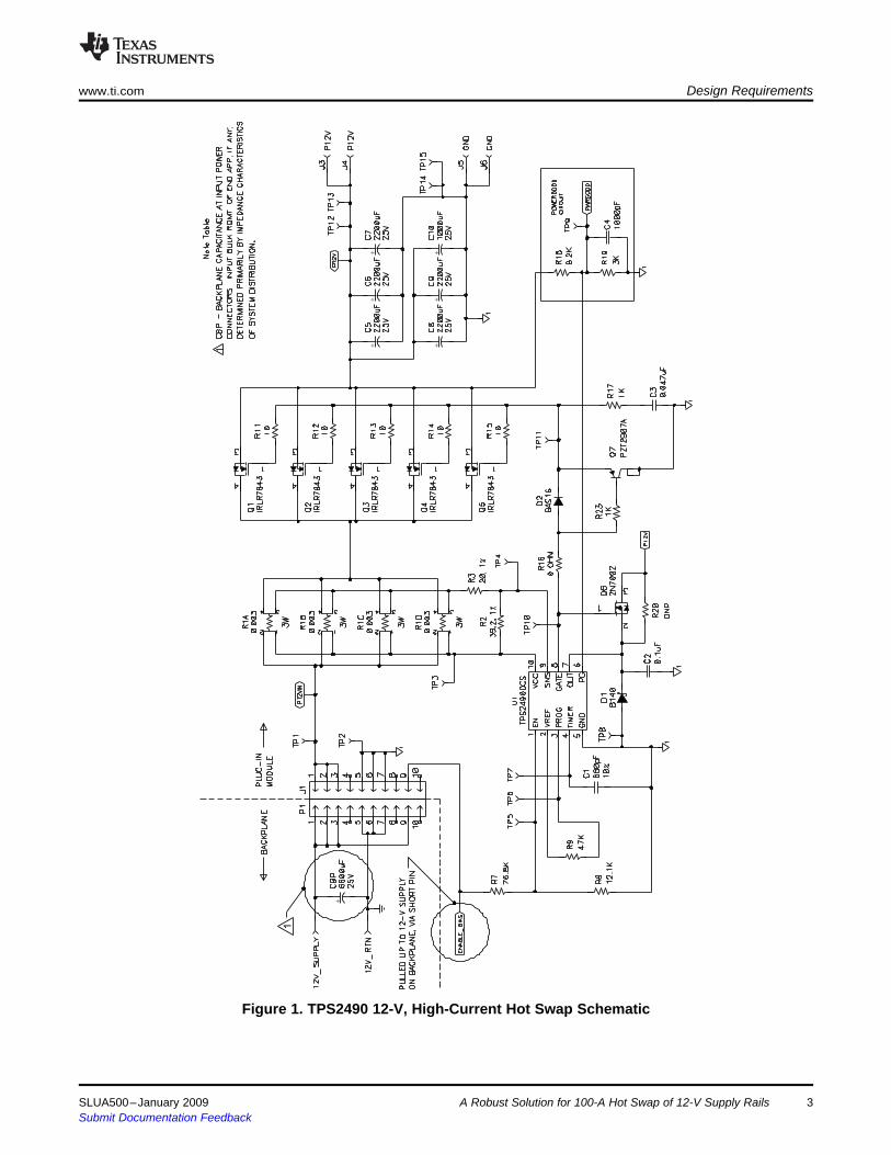
In the schematic, the TPS2490 is shown controlling five IRLR7843 N-Channel MOSFET’s. The numberand type of pass FET is easily tailored to the load requirements of the target application. Load currentmagnitude is fed to the TPS2490 SNS pin via the scaling network of R1, R2 and R3. The current sensenetwork determines the circuit threshold for fault current detection and limiting. Other circuit parameters(turn-on voltage threshold, fault timer interval) are programmed by the passives to the left of the U1symbol (i.e., R7, R8, R9, C1). Output sensing, inrush control, and a fast gate pull-down circuit are to theright (i.e., Q6, R17, C3, D2, R23, and Q7). The details of component selection and sub-circuit operationare discussed in detail in later sections of this document. Finally, the bank of large capacitors connectedacross the output (P12V) to GND (C5 – C10) represents the load capacitance which may be present asthe input bulk capacitance of downstream circuitry, such as Point-of-Load (POL) converters.
The circuit presented in Figure 1 was designed for the following system requirements and loaddescription:
Table 1. System RequirementsPARAMETER VALUE
Input supply voltage, VIN 12 V, 10%Maximum steady-state load, IL(max) 80 A
Load input bulk capacitance 10,000 µF, ± 20%Output turn-on threshold 10.5 V maximum
Logic-level PowerGood (PG) output active-high, LVC/ALVC CMOS compatible, 3.3-V systemMax. ambient operating temperature 60°C
No external heat sinks
A Robust Solution for 100-A Hot Swap of 12-V Supply Rails2 SLUA500–January 2009Submit Documentation Feedback
1
++
++
++
+
www.ti.com Design Requirements
Figure 1. TPS2490 12-V, High-Current Hot Swap Schematic
SLUA500–January 2009 A Robust Solution for 100-A Hot Swap of 12-V Supply Rails 3Submit Documentation Feedback

4 Preliminary Design Considerations -- Inrush Control SchemePreliminary Design Considerations -- Inrush Control Scheme www.ti.com
Given the high current which the hot swap circuit must be able to source, some thought should be givenup front to what type of inrush control scheme to use. Control methods basically fall into two maincategories; constant current, in which the pass FET is operated as a limited current source, and voltagemode (or dV/dt), in which the load voltage rate of rise is controlled in such a manner that the resultant bulkcap charging current is limited below a pre-determined level. There are of course variants of each type.
Traditional constant-current controllers are beneficial in that they offer very predictable and repeatablecurrent limiting, regardless of variations in input voltage or load capacitance, or the fault status of the load.They do have a drawback though, in that they must be allowed at start-up to operate at least long enoughto account for the anticipated worst-case bulk charging time. For applications with high nominal inputvoltages, or large load capacitance, this may lead to setting extended fault time-out delays. Unfortunately,extended delay periods make it difficult to protect the pass FET(s) in other scenarios, such as turning oninto a shorted load, or overcurrent faults during steady-state operation. So at least at first glance, onereason for selecting the TPS2490 for this application is that it adds pass FET VDS sensing, and uses thisinformation to vary the current limit threshold to maintain a constant power dissipation in the FET. Thisfoldback mechanism protects the pass FET from excessive stresses in the case of a faulted load.
In order to set the limits for the internal constant-power engine, an appropriate dissipation limit must beestablished for the FET. Generally, this is done by considering the maximum operating junctiontemperature (TJ) rating of the device, and selecting limit values to remain below that temperature atextremes of ambient operating temperature and load range. A number of thermal calculators, from simplespreadsheets to complex PCB thermal analysis tools, are available for this purpose. On the simpler side,one might consult the design procedure in the APPLICATION INFORMATION section of the TPS2490data sheet[1]. Alternatively, an Excel spreadsheet calculator tool is available from TI which automatescalculation of a FET transient power limit[2]. Links to these resources are listed in the reference section ofthis document. The reader is referred to these, as determination of a dissipation limit is beyond the scopeof this application note. However, Chapter A contains some important background information regardingthe technique of using parallel FET’s to reduce overall RDS(on), and increase the dissipation capability of,the hot swap “switch”.
Applying the guidelines in Chapter A, a maximum transient dissipation limit of 48 W was established forthis example design. This limit is based on the following FET selection and specifications:
Table 2. FET Selection and SpecificationsPARAMETER VALUE
International Rectifier IRLR7843FET type
Five (5) FET’s in parallelMaximum junction temp, TJ(max) 175 °C
3.3 mΩ (at TJ = 25 °C)Maximum RDS(on) 4.3 mΩ (at TJ = 105 °C)
Package D-PAKMax. Thermal Impedance, J - A, RθJA 40°C/W(3)
Using the equations in the TPS2490 data sheet, it was determined that a programming voltage of lessthan 50 mV must be applied to the PROG pin to establish the above power limit. Given normal devicetolerances as stated in the data sheet, it was considered that the resultant power limit percent variationfrom board to board may be unacceptable. Therefore this circuit actually disables the constant powerfeature of the TPS2490, and configures the device in a dV/dt control scheme for turn-on events. Thedevice’s current limiting control still manages load faults during subsequent steady-state operation. The47-kΩ pull-up on the PROG input to the VREF pin disables power limiting.
A Robust Solution for 100-A Hot Swap of 12-V Supply Rails4 SLUA500–January 2009Submit Documentation Feedback

5 Design Procedure
5.1 Setting the Fault Trip (Current Limit) Threshold
501 0 5
100
SNS
LIM
V mVR . m
I A= = ´ W
(1)
1
2 3 31
SNS SNS
SNS SNS LIM SNS
V VR R R
V V I R V= ´ = ´
- ´ -(2)
www.ti.com Design Procedure
The load current sense signal is developed as the voltage drop across sense resistor R1, and appliedacross the VCC and SNS pins of the TPS2490. The TPS2490 has a fixed current limit threshold. Theaction of the internal control amplifier is to slew the pass FET gates to limit the sense voltage to thisthreshold, typically 50 mV. Despite the fixed device threshold, and even with a potentially limited set ofdiscrete sense resistor values, a fine degree of limit resolution can still be achieved. If needed, the dividernetwork of R2 and R3 can be used to scale the input to the TPS2490 to obtain the desired set point,which is demonstrated in the below design process.
The current sourcing limit should be selected to allow some margin over the steady-state load current forsystem noise and component tolerances. For this solution, a margin of 25% was chosen, for a nominalcurrent limit of 100 A. The sense resistor value is then determined as:
If the calculated value of sense resistor is not readily available, first determine an acceptable combinationresulting in a somewhat higher equivalent resistance. For example, the four (4) 3-mΩ sense resistorsshown in the Figure 1 schematic yield an effective 0.75-mΩ sense resistor. Resistors R2 and R3 are thenselected to scale the voltage applied to the TPS2490 inputs. Referring to Figure 1, the voltage across R2is applied to the TPS2490 pins, so the divider equation yields:
Where:• VSNS is the TPS2490 internal threshold (50 mV nominal)• VSNS1 is the drop across element R1, in mV, and• ILIM is the desired sourcing limit in amps.
Note that SNS pin bias current through resistor R2 produces an error component in the measured current.Therefore, the divider impedance must be kept low in order to minimize this error contribution. As ageneral guideline, an overall impedance of 100 Ω or less is good. For this example, setting R3 to 20 Ω,1% value produces an R2 value of 40 Ω. The 1% value of 39.2 Ω was selected.
SLUA500–January 2009 A Robust Solution for 100-A Hot Swap of 12-V Supply Rails 5Submit Documentation Feedback

( )2
1 1
SNS(min) BIAS MAX DIVLIM(min) DIV
LIM(min)
MAX MAX
V I R / AV / AI
R R
- ´= =
(3)
[ ]
( )
45 20 1 01 39 2
39 2 59 288 1
1 01 0 75LIM(min)
mV ( A) ( . ) ( . )
. / .I . A
( . ) ( . m )
m- ´ ´ W
= =´ W
(4)
5.2 Establishing the Inrush Limit
0
2
MAX
AVG
PP
+=
(5)
LOAD OUT
ON
MAX
C dVt
I
´=
(6)
Design Procedure www.ti.com
Once the actual resistor values are selected, it’s a good practice to calculate the worst-case minimumthreshold that may be encountered, accounting for sense resistor and TPS2490 threshold tolerances. Thisminimum sourcing level must be greater than the maximum load to prevent unwanted limiting operation(and potential load shutdown) during normal operation of the card. For the sense voltage dividerconfiguration, this minimum current is given by Equation 3.
Where:• ILIM(min) is the minimum sourcing level of the circuit, in amps,• VSNS(min) is the TPS2490 minimum current sense threshold,• R1MAX is the maximum sense resistor value, in milliohms, and• ADIV is the gain of the divider.
The TPS2490 data sheet specifies VSNS(min) (without power limiting) to be 45 mV; the sense pin biascurrent is 7.5 µA typical, 20 µA maximum. Substituting the circuit values into Equation 3 yields Equation 4:
Even with the (1%) resistor tolerances applied to the divider factor in the above, Equation 4 still returns aresult of 87.56 A, indicating sufficient margin exists over the expected load.
This section discusses the procedure for choosing the value of the gate capacitor (C3 in Figure 1) to setthe inrush current limit. The circuit charges up the load bulk capacitance by ramping the common FETgates node at a constant rate, with the sources following by one VGS drop. A maximum charging current isestablished according to the primary application criteria. Then, the rate of rise is limited to maintain thesourced current below this maximum. The calculation process works by considering that turning on theload in this fashion requires delivering a certain amount of charge to the FETs’ gate capacitance in a fixedamount of time. The fact that multiple FET’s are paralleled, due to steady-state dissipation requirements,is actually beneficial with this method, due to the amount of capacitance already present on the node. Themaximum rate at which charge can be delivered by the TPS2490 is considered, and if needed, C3 isselected as an additional reservoir in which to dump charge.
As discussed earlier, the dominant criteria in selecting the inrush current limit was to limit the powerdissipated in any one of the pass FET’s to 48 W during turn-on events. Assuming constant-currentcharging of the load bulk capacitance (a reasonable approximation), the instantaneous FET dissipation willstart at some quantity PMAX, then decay linearly (with decreasing VDS), to zero watts at the end of theramp period. Therefore, the average dissipation during start-up can be simplistically represented as:
This relationship indicates an allowable peak power of PMAX = 2 x PAVG, or 96 W.
Since, for a given current through the FET, the worst-case stress will occur at the maximumdrain-to-source voltage, the maximum supply condition was used to establish the current limit. So thismaximum current was set to IMAX = PMAX / VMAX = 96 W / 13.2 V, or 7.27 A. For a primarily capacitive loadat start-up, the time required to charge the load cap at this rate, tON, is given by Equation 6.
6 A Robust Solution for 100-A Hot Swap of 12-V Supply Rails SLUA500–January 2009Submit Documentation Feedback

( )1MAX LOAD OUT
ON LOAD LOAD
MAX LOAD
I R dVt R C ln
I R
é ù´ -= - ´ ´ ´ ê ú
´ë û (7)
CHG(max) ON G
EXT
G
i t dQC
dV
´ -=
(8)
[ ]35 20 5 300 037
15EXT
( A) ( mS ) nCC . F
V
mm
´ - ´= =
(9)
www.ti.com Design Procedure
If the downstream load on the hot swap circuit is better modeled as an RC-type load (at load turn-on),Equation 7 is an alternate form which may more accurately estimate the start-up time, tON. However, thedesigner must take precautions that a certain fundamental relationship is maintained. If the resistivecomponent of the load model is such that VIN(max) / RLOAD > IMAX, the implication is that the current-limitedsource cannot develop the input supply potential across the load. The programmed sourcing limit may beexceeded in order to fully charge the load.
For this design, with the use of the circuit PWRGOOD output to enable downstream converters, the loadwas considered primarily capacitive. For the nominal supply voltage of 12 V (and therefore, dVOUT = 12 V),Equation 6 returns an interval of tON = 16.5 ms. To keep actual, in-circuit dissipation conservative relativeto calculated results, the target start-up interval was rounded up to 20 ms.
Referring to the IRLR7843 data sheet, the typical gate charge curve shows a total gate charge, from 0 Vto the end of the plateau at VGS ~= 3 V, of 30 nC. (A rough interpolation is fine for this calculation.) Also,to maintain this VGS throughout the output ramp-up event, the gate will have to be ramped to 12 V + 3 V =15 V. Summing the charge that must be delivered to bring up the load, and equating that to the maximumcharge that could be delivered by the TPS490, the relationship can be rewritten to determine the minimumexternal gate capacitance needed to limit the ramp-up rate. The result is Equation 8.
Where:• iCHG(max) is the maximum sourcing current of the TPS2490 GATE pin, 35 µA per the data sheet,• tON is the calculated start-up interval from Equation 6 or Equation 7, as adjusted,• dQG is the total FET gate charge, and• dVG is the delta-V at the common gates node during the output ramp.
Substituting the application values into Equation 8 produces:
The next higher standard available value of 0.047 µF was selected for C3.
SLUA500–January 2009 A Robust Solution for 100-A Hot Swap of 12-V Supply Rails 7Submit Documentation Feedback

Ch. 1 = VIN
VEN
VOUT
IIN
(2 A/div.)
Design Procedure www.ti.com
Figure 2 is a scope capture of a circuit turn-on event from the TPS2490 EN pin assertion (TP5 node inFigure 1), with a nominal 12-V input supply potential. The test load, as shown in Figure 1, was 12,000 µF,to look at performance allowing for the 20% bulk capacitor tolerance indicated in the design specification.
Figure 2. Start-Up Event Into 12,000-µF Load, From EN Pin Assertion.
Note that the circuit maintains a constant current to the load during bulk capacitor charging (inrushcurrent). The current limit level was about 4.4 A, significantly lower than the target of 7.27 A. Accordingly,the load ramp-up time, from 0 V to 12 V, was measured (with scope cursors, not shown) to be slower thanthe targeted interval, at 32.4 ms. The bulk of this difference can be attributed to the C3 selected value27% larger than the calculated result, and what’s most likely a much more nominal GATE pin sourcedcurrent versus the maximum value used. This shows the level of conservatism built into the componentselection, and one could even argue that there’s margin to reduce the value of C3. On the other hand, thestart-up waveforms clearly demonstrate that inrush current is managed to such a benign level that it’seasily handled by any one of the five FET’s, even after operation at elevated junction temperatures.
A Robust Solution for 100-A Hot Swap of 12-V Supply Rails8 SLUA500–January 2009Submit Documentation Feedback

5.3 Circuit UVLO Considerations and Threshold
( )12
8 7EN _ L
UVF( V ) EN _ L
VR R
V V= ´
-(10)
www.ti.com Design Procedure
The input voltage range in this application is such that he TPS2490 is operated fairly close to its ownsupply UVLO threshold. Experience has shown that, in a situation of decreasing supply voltage, the outputshutdown action is more definitive if performed prior to reaching the VCC UVLO, as opposed to relying onthe UVLO shutdown response. The solution uses the device enable pin (EN) with the resistive divider ofR7 and R8 to establish a circuit UVLO threshold. The design goal then was to keep the minimum fallingUV threshold, as established by the EN pin, above the maximum VCC falling UVLO threshold. Note thatthe TPS2490 data sheet does not specify a maximum limit for the “VVCC turn off” parameter, nor aminimum hysteresis for this pin. Without these specifications, one way to guardband the externalprogrammed threshold is to use the maximum “VVCC turn on” limit, 8.8 V -- the input falling threshold hasto be less than that.
A value for resistor R8 is calculated from Equation 10.
Where:• VEN_L is the EN pin switching threshold, for falling input voltage, 1.22 V min., and• VUVF(12V) is the desired UV threshold at the input supply rail.
To calculate the divider string values, a secondary guideline is to establish a minimum divider load of 50µA, as this minimizes errors due to EN pin bias current. For this application, this translates to a totaldivider impedance of less than 170 kΩ (at 8.5 V). With R7 set to 76.8 kΩ, and using the voltage valuesindicated above, this produces a value for R8 of 12.36 kΩ. By opting for the closest value less than thecalculated result, the minimum VUVF(12V) threshold is kept above the target value.
SLUA500–January 2009 A Robust Solution for 100-A Hot Swap of 12-V Supply Rails 9Submit Documentation Feedback

5.4 Setting the Fault Timeout Period
CHG FLT
FLT
i tC
dV
´=
(11)
25 100625
4FLT
( A) ( S )C pF
V
m m´= =
(12)
Design Procedure www.ti.com
As discussed previously, one of the caveats of constant-current inrush control is that any fault timer mustbe set long enough to allow fully discharged bulk capacitance to charge during turn-on events.Conversely, a benefit of the dV/dt load ramp as used here is that the inrush limit can be set below theoverload fault threshold. This can be beneficial in applications where a large amount of input bulkcapacitance must be charged. Maintaining inrush below the fault threshold holds the timer off duringstart-up of a valid, non-faulted load. Therefore, fault time-out periods can be kept short enough to keepFET dissipation within the SOA rating of the FET, but long enough to avoid nuisance trips due to loadsurges or system noise. As always, the FET manufacturer’s data sheet should be consulted to verifyapplicable pulse duration limits will not be exceeded in the situation of a load short at the card’s operatingvoltage. Referring to the IRLR7843 data sheet Maximum Safe Operating Area graph, for a VDS of 10 V,safe operation limit is indicated as just over 100 A for up to 100 µs. Therefore, the fault time selected wasa nominal 100 µs.
Since fault timing is accomplished by the constant-current charging of the external timing capacitor (C1) toa trip threshold, the timing capacitor value is determined from Equation 11.
Where:• CFLT is the fault capacitor value,• iCHG is the TIMER pin sourced current during faults,• tFLT is the desired fault time-out period, in seconds and• dV is the delta-V to be developed across the capacitor, charging from 0 V to the TPS2490 fault
threshold.
TIMER pin current in µA returns a capacitor value in µF. Substituting the TPS2490 data sheet values intoEquation 11 produces:
The next higher standard value of 680 pF was selected for C1.
A Robust Solution for 100-A Hot Swap of 12-V Supply Rails10 SLUA500–January 2009Submit Documentation Feedback

5.5 Powergood Output Generation
12
19 18OH(min)
MIN
P V (min) OH(min)
VR R
V V= ´
é ù-ë û (13)
www.ti.com Design Procedure
The TPS2490 PG pin is an active-high, open-drain output which, after a deglitch delay, becomes highimpedance when output voltage conditions meet the criteria. (Please refer to the TPS2490 data sheet.)The PG pin can be pulled up to essentially any available supply to generate the logic high output level. Forthis design, it was decided to use the 12-V output to provide the bias, and simply divide the voltage downfor the desired signal levels.
The TPS2490 data sheet indicates an absolute maximum sink current for this pin of 10 mA. For themaximum input supply in this application of 13.2 V, this limit suggests a minimum value for R18 of around1400 Ω (allowing for a 5 % tolerance). Setting R18 to 8.2 kΩ sets a nominal output current of about 1.5mA.
Presuming this output should remain a valid logic high level down to the minimum circuit UVLO voltage,then the value of the bottom leg of the divider can be calculated from :
Where:• VOH is the high-level output voltage of the PWRGOOD signal, and• VP12V is the output voltage rail potential.
Substituting in a minimum VOH of 2 V, and the minimum UV threshold of 8.8 V as designed in Section 5.3,Equation 13 returns a value of 2.4 kΩ for R19. R19 was set to 3 kΩ to provide some margin above theabsolute minimum input voltage requirement for the selected logic family.
The selected resistor values produce a nominal VOH of 3.21 V at the nominal 12-V output voltage.
SLUA500–January 2009 A Robust Solution for 100-A Hot Swap of 12-V Supply Rails 11Submit Documentation Feedback

6 Enhancing Shutdown Performance
6.1 OUT Pin “Isolation”
+
14V+
V(DS)
Charge
Pump
Constant
Power
Engine V( LIM)Gate Control
Amplifier
Current Sense
Amplifier
10
9
8
7
GATE
OUT
VCC
SENSE
Enhancing Shutdown Performance www.ti.com
The TPS2490 gate drive circuitry includes an active clamp at the output (GATE pin). Functionally, thisclamp can be represented as a 14-V Zener connected from GATE (cathode) to OUT. (See Figure 3.) Thisclamp serves the purpose of protecting the external pass FET’s against damage from excessive gatevoltage. However, in a load shutdown event, regardless of trigger, this “diode” becomes forward biased,now clamping the GATE pin, and hence, the FET gate(s), one diode drop below the output potential. In atraditional TPS2490 application, where the input supply is most often a nominal 48 volts, this also serves apurpose, protecting the FET gates from excessive negative VGS excursions. However, for low voltageapplications, the turn-off performance can be improved with a simple trick.
Figure 3. Gate Drive with Output Clamp
Figure 4 and Figure 5 shows a comparison of the shut-down response of the circuit of Figure 1, for twodifferent configurations. In both events, 12,000 µF of bulk capacitance is connected to the output (P12V),and a 20-A constant-current load is applied. Figure 4 shows the resultant GATE and output waveformswhen the OUT sense pin is connected directly to the output node (i.e., if R20 were 0 Ω). Note that the totaldecay time of the output from 12 V to 0 V was about 6.9 ms; this corresponds quite well to the calculatedperiod of 7.2 ms, indicating that the discharge profile is dictated by the load current. But because of thenow forward-biased clamp, the FET gates follow this linear decay all the way down, offset by one diodedrop. So in effect, the load bulk capacitance “holds up” the FET gates.
12 A Robust Solution for 100-A Hot Swap of 12-V Supply Rails SLUA500–January 2009Submit Documentation Feedback

VGATE
(at TP10)
Ch. 3 = VOUT
VGATE
(at TP10)
VGATE
(at TP10)
Ch. 3 = VOUT
www.ti.com Enhancing Shutdown Performance
Figure 4. Gate pull-down profile at load Figure 5. Gate pull-down profile at loadshut-down (OUT pin direct connect ) shut-down (FET Q6 installed)
While in the event of Figure 4 the pass FETs are technically off, there is a drawback to this characteristic,particularly when operating close to the TPS2490 input UVLO threshold, as in this application. In therelatively benign lab environment, where perhaps only one input is exercised in any test, the turn-off action(GATE pin pull-down) is smooth and consistent. However, in a much noisier actual system, or underheavier load where the input supply may make a step recovery when the current is interrupted, the eventmay not be as clean. More specifically, if the input potential drops below VCC UVLO, the GATE pull-downmay not be as consistent. Considering the gate potential is not much below the FETs’ VGS(TH) voltage, of atypical power MOSFET, if doesn’t take much for the decaying output voltage to pull the common FETsources below the ON threshold. The worst-case is if the input supply begins to oscillate about the UVLOwindow. In order to better protect the FET’s from indefinite operation in linear mode, it’s highly preferableto get the FET gates pulled low as quickly as possible.
Therefore, it is recommended to insert FET Q6 between the TPS2490 OUT pin and the actual output node(R20 is not installed). Driven by the same output as the pass FET’s, Q6 acts as a switch to perform anoutput disconnect function, or “isolate” the pin from the bulk cap during shut-down. During a turn-on eventand subsequent card operation, Q6 is on, and connects OUT to P12V for powergood sensing. However, ina shutdown event, when Q6 turns off, the OUT pin is disconnected from the load. The GATE pin is nolonger pinned to the output potential and inherent hold-up action of the potentially large bulk capacitance.
Figure 5 is an example of the same type of shutdown event when Q6 is installed. Note that while theoutput decay time (6.8 ms) is still dictated by the load on the circuit, the gates are pulled rapidly to ground.Consequently, the shutdown response is much more definitive than in Figure 4.
SLUA500–January 2009 A Robust Solution for 100-A Hot Swap of 12-V Supply Rails 13Submit Documentation Feedback

VGATE
(at TP10)
Ch. 3 = VOUT
Ch. 1 = VEN
Enhancing Shutdown Performance www.ti.com
Figure 6. GATE pin discharge time, VGS = 0 V to VGATE = 1 V
As a figure of merit for comparing different OUT pin “isolation” tricks, the residual gate discharge time, thatis, the time to bring the gates from a condition of “FET’s off” to a gate voltage of 1 V, was examined.Figure 6 is a scope capture of a similar shutdown event, under the same conditions as in Figure 4 andFigure 5, on an expanded time base. Taking the FET’s off condition to be the point at which the GATEtrace passes through the output potential (i.e., VGS = 0 V), the discharge time to VGATE = 1 V wasmeasured to be 890 µs. This results in a significant safety margin for the hot swap circuit. Note that theresidual gate discharge time is very consistent at 850 – 900 µs under the full range of load currents.
A Robust Solution for 100-A Hot Swap of 12-V Supply Rails14 SLUA500–January 2009Submit Documentation Feedback

6.2 Fast Gate Pull-down Circuit
Ch. 3 = VOUT
IIN
(50 A/div.)
VGATE
(at TP10)
VGATE
(at TP10)
VTIMER
IIN
(100 A/div.)
www.ti.com Enhancing Shutdown Performance
An additional though unintended benefit of using multiple, large pass FET’s as done here is the inherentlarge amount of gate capacitance, which is conducive to the dV/dt ramp control. However, that extracapacitance is detrimental to turning the FET’s off quickly. While the TPS2490 GATE pin sink capabilitycan discharge the FET gates, turn-off under severe fault conditions may not be fast enough. A simple,three component circuit should be added to the gate drive circuit to easily address this.
The circuit of D2, R23 and Q7 comprises a fast gate pull-down mechanism to quickly turn off the passFET’s. D2 simply performs a blocking function. When the TPS2490 GATE pin pulls low (in response toany condition), rather than discharging the FETs’ input capacitance directly, the GATE pin now pulls basecurrent from transistor Q7, which in turn applies a much stronger discharge current to the gates.
The fast pull-down is beneficial in a couple of circumstances, with one of these situations being the morecritical. For example, during shutdown from EN pin command as discussed in Section 6.1, the fastpull-down greatly reduces the time to turn the FET’s off. Referring to Figure 4, Figure 5 and Figure 6, thisis the interval from EN deassertion until the gate is pulled below the FET ON threshold; at the time base ofthese figures, essentially the point at which the gate trace passes through output node potential. Thetypical turn-off time of 450 to 600 µs without the external circuit is reduced to only about 2.5 µs when thepull-down circuit is added.
More importantly though is the corresponding improvement in response to a severe overload, or outputshort-circuit condition. Figure 7 and Figure 8 are waveform captures of various nodes and the load currentduring short-circuit events. In both tests, the output is ramped up, then an initial operating load of 40 A isapplied via electronic load. The short-circuit condition is then generated by depressing the load SHORTbutton.
In both instances, the fault current profile is essentially as expected. The sudden excursion over the faultthreshold causes a hard gate pull-down to clip the current as quickly as possible. Once the current isbrought back below threshold, the TPS2490 turns the FET’s back on slowly, in linear mode to “test” thepersistence of the fault. This is when the fault timer is started. If the fault condition endures beyond theperiod of the timer, as below, the FET’s are turned off.
Figure 7. Short-Circuit Event, With 40-A Figure 8. Short-Circuit Event, With 40-APre-Fault Steady-State Load (without gate Pre-Fault Steady-State Load (external gate
pull-down circuit ) pull-down installed)
(Channel 4 (load current) baseline is two-tenths of a division from the bottom of the screen.)
SLUA500–January 2009 A Robust Solution for 100-A Hot Swap of 12-V Supply Rails 15Submit Documentation Feedback

Ch. 3 = VOUT
IIN
(50 A/div.)
VGATE
(at TP10)
Enhancing Shutdown Performance www.ti.com
However, there are differences in the severity of the event between the two cases. In Figure 7, without theexternal pull-down circuit, the initial peak current spike reached about 230 A. Also, during the linear modeportion of the event, when the GATE tries to follow the decaying output node to slew the load current, thesourced current remains high. In fact, by the end of the fault timer period, the “regulated” load current isstill 170 – 180 A. Compare this to the magnitudes captured in Figure 8, where the fast pull-down wasused. Using scope cursors (not shown), the initial spike peak amplitude was measured to be 194 A, asignificant reduction over the Figure 7 spike. Also, the TPS2490 is able to fold back the current to 112 Aduring the ensuing linear mode operation. Ultimately, the total interval elapsed above the programmed100-A trip point, including the initial spike, is only 127 µs.
Figure 9 shows another short-circuit event. In this instance, the initial steady-state (pre-fault) load was 80A. Again, using scope cursors (not shown) to obtain numeric results, the peak current was found to beonly 181 A, with a final regulation point of 106 A.
Figure 9. Short-circuit event with 80-A initial load, and fast gate pull-down installed.
(Channel 4 (load current) baseline is two-tenths of a division from the bottom of the screen.)
A Robust Solution for 100-A Hot Swap of 12-V Supply Rails16 SLUA500–January 2009Submit Documentation Feedback

7 Power Dissipation Datawww.ti.com Power Dissipation Data
The circuit of Figure 1 was laid out on a PCB and assembled for testing, primarily to validate the conceptof passing up to 80 A through the hot swap circuit without the use of heat sinks. Recall that the feasibilityof the design is predicated to some degree on the ability to achieve the FET manufacturer’s stated RθJA, orbetter, even with five co-located drain tabs discharging heat into the PCB copper pours. Eight layers ofPCB thermal plane were used, with 2 oz. copper. Thermal layers were split essentially equally (4 each)between the supply high-side current path and the return (GND) node. The overall dimensions of theplanes were approximately 5.5” x 3.5”, but also encompassed patterns and keep-outs for the followinglarge-size components:• Six (2 supply, 4 load) 0.800” x 0.600” patterns for #2 solderless connector lugs• Eight patterns for 12.5-mm dia. aluminum electrolytic radial-lead capacitors (test load)
Table 3 shows the dissipation associated with the various voltage drops across the high-current path ofthe PCB, both high-side components and plane areas, and the return plane. Dissipation was determinedby measuring the voltage drops across each element in the current path, and calculating the power lossas the VxI product. Note that at these load currents, the voltage drops across not only components suchas sense resistors and FET’s but also copper pours themselves are significant, and contribute to the heatwhich must be dissipated by the PCB. Table 4 lists the definitions of the various dissipation nodes(Table 3 column headings) recorded. The circuit and layout were found to have a minimum efficiency (at80 A) of 98.6%
Table 3. Dissipation Losses Across PCB High-current Path. (1) (2)
ILOAD PINP PRSNS(each) PTHP PSW(each) POUTP PRTN PD-TOT EFFICIENC(A) (mW) (mW) (mW) (mW) (mW) (mW) (mW) Y
(%)10 3.3 18.7 2.6 11.1 14.0 41.4 192 99.820 14.2 75.2 10.6 44.9 55.9 167.0 773 99.730 30.6 168.9 24.3 102.3 127.8 379.5 1749 99.540 56.0 300.2 44.0 185.3 228.2 684.8 3140 99.450 79.5 469.4 71.0 297.0 357.0 1092.0 4962 99.260 116.4 675.6 105.0 438.5 527.7 1605.0 7249 99.070 161.0 918.6 145.6 619.8 728.7 2246.3 10055 98.880 218.4 1200.6 198.4 843.8 964.0 3019.2 13422 98.6
(1) Tests conducted with PCB resting on a lab bench at room ambient temperature (~25 °C), natural convection only.(2) At each test current, input supply margined to maintain 12.00 ± 0.02 VDC at PCB input terminal lugs.
Table 4. Power Dissipation Element Definitions.NAME ASSOCIATED POWER DISSIPATIONPINP Input copper plane, from P12VIN connector pattern sensed at lug, to thermal via
centrally located within sense resistor patterns.PRSNS Sense resistors (each), measured across Kelvin-connected TP3 to TP4.PTHP Component thermal plane, from thermal via centrally located within sense resistor
patterns, to Q3 (center FET) drain tab.PSW FET switches (each), measured across Q1 (largest drop of the 5 FET’s)
POUTP Output copper plane, average from FET sources to J3/J4 patterns sensed at lugs.PRTN Current return plane, from a Kelvin “average” sense of J5/J6, to 12V_RTN sensed at
input connector lug.PD-TOT Total, sum of the losses across the board.
SLUA500–January 2009 A Robust Solution for 100-A Hot Swap of 12-V Supply Rails 17Submit Documentation Feedback

Power Dissipation Data www.ti.com
Infrared camera measurements taken at 80-A load indicated that the hottest components were actually thesense resistors. The temperature of the FET cases and immediately surrounding PCB areas was about70°C, suggesting junction temperatures not much higher than that. Given the maximum operating junctiontemperature of the IRLR7843 of 150°C, these results suggest sufficient margin to operate the circuit at fullload at the specified design target TA of 60°C. The forced air convection typical of the target rack andchassis environments would of course enhance thermal performance, further protecting the hot swapFET’s.
For comparison with competing hot swap controllers and solutions, Table 5 summarizes the test results forthe same circuit and PCB layout, but with only a 5-V gate drive. To conduct the test, a 5.1-V Zener diodewas connected from FET gate to source nodes, to clamp the GATE output voltage of the TPS2490. Testresults demonstrated that FET dissipation was 21 to ~25% higher than with the full gate drive,exacerbating heating of the FET junctions. The relative increases for given load currents are shown in thetable, along with the net change in total dissipation of the board (PD-TOT). The dissipation of the otherresistive drops was essentially unchanged, so those values are not shown in the table.
Table 5. Comparative Dissipation with 5-V Gate DriveILOAD DISSIPATION, VGS = 5 V % DELTAS vs. TPS2490 GATE DRIVE
PSW (each) PD-TOT PSW(each) PD-TOT
(A) (mW) (mW) (%) (%)10 13.5 21.020 54.6 822 21.6 6.330 124.1 21.340 226.1 3337 22.0 6.350 364 22.660 540.1 7761 23.2 7.170 766.4 23.780 1051.4 14484 24.6 7.9
Table 6 lists the dissipation values with only 4 parallel FET’s installed on the board, to examine thefeasibility of reducing the number of FET’s. To maintain the layout symmetry, the middle FET of theoriginal 5-FET pattern was removed from the board to conduct this test. As shown in Table 6, the powerloss in the FET’s rose sharply, 59% higher than in the 5-FET configuration at the 70 and 80 A points. Also,unlike the results with the reduced gate drive, this experiment resulted in increases in the two adjacentplane areas. While any of the absolute data values are specific to the layout of the test board, the percentchanges provide designers with a relative comparison for determining how many FET’s to use in theirapplication. A smaller number of FET’s may be appropriate where a given cooling airflow rate or differentFET package will produce a better effective thermal impedance. Also, the table below may serve as areference for determining number of FET’s when the target load is something less than 80 A.
Table 6. Circuit Dissipation Results Using Four Parallel FET’sILOAD DISSIPATION, 4-FET CONFIGURATION PERCENT DELTAS VS. 5-FET RESULTS
PTHP PSW (each) POUTP PD-TOT PTHP PSW(each) POUTP PD-TOT
(A) (mW) (mW) (mW) (mW) (%) (%) (%) (%)10 2.8 17.2 15 7.7 54.7 7.220 11.4 69.4 58.5 828 7.5 54.6 4.7 7.130 25.5 158.7 133.4 4.9 55.1 4.340 47.2 290.2 240.8 3394 7.3 56.6 5.5 8.150 75.5 463.4 376 6.3 56 5.360 111 687.2 560.7 7846 5.7 56.7 6.3 8.270 158.9 985.3 790.3 9.1 59 8.580 215.2 1340.4 1048.4 14662 8.5 58.8 8.8 9.2
A Robust Solution for 100-A Hot Swap of 12-V Supply Rails18 SLUA500–January 2009Submit Documentation Feedback

8 Conclusion
9 Footnotes
10 References
www.ti.com Conclusion
A solution schematic was presented for hot swap control of a 12-V rail with up to 80-A load, based on theTPS2490 Hot Swap Controller. A design process was outlined, with appropriate equations, for designersto tailor the solution to the requirements of their own systems. Some related topics, such as choice ofinrush limiting scheme, circuit UVLO considerations, and improving the shutdown response werediscussed, so that the reader can understand how to configure the TPS2490 for this type of application. Afew scope captures of operational events were presented to demonstrate circuit performance. Finally,some power loss data from a representative layout was presented, for comparison against alternatesolutions, and to help the reader tailor the number of FET’s for the load level, cooling provisions, andMOSFET thermal characteristics specific to his or her design.
In summary, the scope plots and data presented here demonstrate that the TPS2490 device can beconfigured as the foundation for a very robust hot swap circuit for 12-V rails at very high currents.
1. The TPS2490 device data sheet is available from the Texas Instruments web site. A download link canbe found on the product page at http://focus.ti.com/docs/prod/folders/print/tps2490.html.
2. A download .zip file with the TPS2490 Calculator Tool Excel spreadsheet is available from the TexasInstruments web site at http://focus.ti.com/docs/toolsw/folders/print/tps2490or91calc.html.
3. The transient dissipation limit of 48 W arrived at through calculations is based on the assumption thatthis effective thermal impedance (40°C/W) can be achieved with the D-PAK package, through acombination of dissipative layout techniques and airflow in the target system.
Data sheet, TPS2490/TPS2491 Positive High-Voltage Power-Limiting Hot Swap Controller, TexasInstruments Literature No. SLVS503, November 2003.
Data sheet, IRLR7843/IRLU7843 HEXFET Power MOSFET, International Rectifier, www.irf.com.
SLUA500–January 2009 A Robust Solution for 100-A Hot Swap of 12-V Supply Rails 19Submit Documentation Feedback

Appendix A Parallel FET’s in Current-Limiting Hot Swap
Appendix A www.ti.com
This appendix contains an important note regarding the use of multiple, parallel FET’s as the limiting“switch” in hot swap applications, such as the one presented in this application note. When evaluatingpotential devices to be used for this purpose, two different operating scenarios must be considered:limiting mode as during inrush control, and load steady-state.
Once the input bulk capacitance of the load has been charged up, the hot swap circuit output is essentiallyat the input supply potential, and the load is operating in steady-state, the parallel FET’s are an effectivemeans of reducing the IR drop of the hot swap switch. The effective resistance of the switch is theequivalent resistance of N resistors of RDS(on) value in parallel, where N is the number of FET’s used. Aslong as good, symmetrical layout practice is used, the FET’s will share current approximately equally, andthe power loss can be calculated as the sum of the resistive losses of ILOAD/N through the RDS(on) of eachFET. Consider the situation in which the card or module has been operating indefinitely at maximumpower, and at the maximum allowed ambient temperature. This dissipation can be used to estimate aworst-case starting junction temperature at which the FET’s may be subjected to the stresses of a turn-onevent.
A load turn-on or output ramping event, however, presents a different situation. During a turn-on event, theFET’s will be operated in the linear region for some period. While in linear mode, there’s no guarantee theFET’s will share current equally. ON-thresholds and transfer characteristics will vary slightly from device todevice. Also, once any one device starts conducting, the typically negative temperature coefficient of theVGS(TH) parameter will decrease the threshold as the device heats up. Therefore, for a robust design, theassumption must be that one FET will turn on first, and conduct all the load current during ramp up.
This characteristic of the parallel FET configuration, along with the worst-case, steady-state junctiontemperature determined per the above, must be used to establish the transient FET power limit duringstart-up events, and in evaluation of SOA ratings of the selected device.
20 SLUA500–January 2009Submit Documentation Feedback

IMPORTANT NOTICETexas Instruments Incorporated and its subsidiaries (TI) reserve the right to make corrections, modifications, enhancements, improvements,and other changes to its products and services at any time and to discontinue any product or service without notice. Customers shouldobtain the latest relevant information before placing orders and should verify that such information is current and complete. All products aresold subject to TI’s terms and conditions of sale supplied at the time of order acknowledgment.TI warrants performance of its hardware products to the specifications applicable at the time of sale in accordance with TI’s standardwarranty. Testing and other quality control techniques are used to the extent TI deems necessary to support this warranty. Except wheremandated by government requirements, testing of all parameters of each product is not necessarily performed.TI assumes no liability for applications assistance or customer product design. Customers are responsible for their products andapplications using TI components. To minimize the risks associated with customer products and applications, customers should provideadequate design and operating safeguards.TI does not warrant or represent that any license, either express or implied, is granted under any TI patent right, copyright, mask work right,or other TI intellectual property right relating to any combination, machine, or process in which TI products or services are used. Informationpublished by TI regarding third-party products or services does not constitute a license from TI to use such products or services or awarranty or endorsement thereof. Use of such information may require a license from a third party under the patents or other intellectualproperty of the third party, or a license from TI under the patents or other intellectual property of TI.Reproduction of TI information in TI data books or data sheets is permissible only if reproduction is without alteration and is accompaniedby all associated warranties, conditions, limitations, and notices. Reproduction of this information with alteration is an unfair and deceptivebusiness practice. TI is not responsible or liable for such altered documentation. Information of third parties may be subject to additionalrestrictions.Resale of TI products or services with statements different from or beyond the parameters stated by TI for that product or service voids allexpress and any implied warranties for the associated TI product or service and is an unfair and deceptive business practice. TI is notresponsible or liable for any such statements.TI products are not authorized for use in safety-critical applications (such as life support) where a failure of the TI product would reasonablybe expected to cause severe personal injury or death, unless officers of the parties have executed an agreement specifically governingsuch use. Buyers represent that they have all necessary expertise in the safety and regulatory ramifications of their applications, andacknowledge and agree that they are solely responsible for all legal, regulatory and safety-related requirements concerning their productsand any use of TI products in such safety-critical applications, notwithstanding any applications-related information or support that may beprovided by TI. Further, Buyers must fully indemnify TI and its representatives against any damages arising out of the use of TI products insuch safety-critical applications.TI products are neither designed nor intended for use in military/aerospace applications or environments unless the TI products arespecifically designated by TI as military-grade or "enhanced plastic." Only products designated by TI as military-grade meet militaryspecifications. Buyers acknowledge and agree that any such use of TI products which TI has not designated as military-grade is solely atthe Buyer's risk, and that they are solely responsible for compliance with all legal and regulatory requirements in connection with such use.TI products are neither designed nor intended for use in automotive applications or environments unless the specific TI products aredesignated by TI as compliant with ISO/TS 16949 requirements. Buyers acknowledge and agree that, if they use any non-designatedproducts in automotive applications, TI will not be responsible for any failure to meet such requirements.Following are URLs where you can obtain information on other Texas Instruments products and application solutions:Products ApplicationsAmplifiers amplifier.ti.com Audio www.ti.com/audioData Converters dataconverter.ti.com Automotive www.ti.com/automotiveDLP® Products www.dlp.com Broadband www.ti.com/broadbandDSP dsp.ti.com Digital Control www.ti.com/digitalcontrolClocks and Timers www.ti.com/clocks Medical www.ti.com/medicalInterface interface.ti.com Military www.ti.com/militaryLogic logic.ti.com Optical Networking www.ti.com/opticalnetworkPower Mgmt power.ti.com Security www.ti.com/securityMicrocontrollers microcontroller.ti.com Telephony www.ti.com/telephonyRFID www.ti-rfid.com Video & Imaging www.ti.com/videoRF/IF and ZigBee® Solutions www.ti.com/lprf Wireless www.ti.com/wireless
Mailing Address: Texas Instruments, Post Office Box 655303, Dallas, Texas 75265Copyright © 2009, Texas Instruments Incorporated