Embed Size (px)
Citation preview
ILI9325
a-Si TFT LCD Single Chip Driver 240RGBx320 Resolution and 262K color
Datasheet Preliminary
Version: V0.35 Document No.: ILI9325DS_V0.35.pdf
ILI TECHNOLOGY CORP. 4F, No. 2, Tech. 5th Rd., Hsinchu Science Park, Taiwan 300, R.O.C. Tel.886-3-5670095; Fax.886-3-5670096 http://www.ilitek.com
a-Si TFT LCD Single Chip Driver
240RGBx320 Resolution and 262K color ILI9325
The information contained herein is the exclusive property of ILI Technology Corp. and shall not be distributed, reproduced, or disclosed in whole or in part without prior written permission of ILI Technology Corp. Page 2 of 111 Version: 0.35
Table of Contents
Section Page
1. Introduction.................................................................................................................................................... 7 2. Features ........................................................................................................................................................ 7 3. Block Diagram............................................................................................................................................... 9 4. Pin Descriptions .......................................................................................................................................... 10 5. Pad Arrangement and Coordination............................................................................................................ 14 6. Block Description ........................................................................................................................................ 21 7. System Interface ......................................................................................................................................... 24
7.1. Interface Specifications .................................................................................................................. 24 7.2. Input Interfaces .............................................................................................................................. 25
7.2.1. i80/18-bit System Interface.................................................................................................. 26 7.2.2. i80/16-bit System Interface.................................................................................................. 27 7.2.3. i80/9-bit System Interface.................................................................................................... 28 7.2.4. i80/8-bit System Interface.................................................................................................... 28
7.3. Serial Peripheral Interface (SPI) .................................................................................................... 29 7.4. VSYNC Interface............................................................................................................................ 34 7.5. RGB Input Interface ....................................................................................................................... 38
7.5.1. RGB Interface...................................................................................................................... 39 7.5.2. RGB Interface Timing .......................................................................................................... 40 7.5.3. Moving Picture Mode........................................................................................................... 42 7.5.4. 6-bit RGB Interface.............................................................................................................. 43 7.5.5. 16-bit RGB Interface............................................................................................................ 44 7.5.6. 18-bit RGB Interface............................................................................................................ 44
7.6. Interface Timing.............................................................................................................................. 47 8. Register Descriptions .................................................................................................................................. 48
8.1. Registers Access............................................................................................................................ 48 8.2. Instruction Descriptions.................................................................................................................. 51
8.2.1. Index (IR)............................................................................................................................. 53 8.2.2. Start Oscillation (R00h)........................................................................................................ 53 8.2.3. Driver Output Control (R01h) .............................................................................................. 53 8.2.4. LCD Driving Wave Control (R02h) ...................................................................................... 55 8.2.5. Entry Mode (R03h) .............................................................................................................. 55 8.2.6. Resizing Control Register (R04h)........................................................................................ 58 8.2.7. Display Control 1 (R07h) ..................................................................................................... 59 8.2.8. Display Control 2 (R08h) ..................................................................................................... 60 8.2.9. Display Control 3 (R09h) ..................................................................................................... 61 8.2.10. Display Control 4 (R0Ah)..................................................................................................... 62 8.2.11. RGB Display Interface Control 1 (R0Ch)............................................................................. 63
a-Si TFT LCD Single Chip Driver
240RGBx320 Resolution and 262K color ILI9325
The information contained herein is the exclusive property of ILI Technology Corp. and shall not be distributed, reproduced, or disclosed in whole or in part without prior written permission of ILI Technology Corp. Page 3 of 111 Version: 0.35
8.2.12. Frame Marker Position (R0Dh) ........................................................................................... 64 8.2.13. RGB Display Interface Control 2 (R0Fh) ............................................................................. 64 8.2.14. Power Control 1 (R10h)....................................................................................................... 65 8.2.15. Power Control 2 (R11h) ....................................................................................................... 66 8.2.16. Power Control 3 (R12h)....................................................................................................... 67 8.2.17. Power Control 4 (R13h)....................................................................................................... 67 8.2.18. GRAM Horizontal/Vertical Address Set (R20h, R21h) ........................................................ 68 8.2.19. Write Data to GRAM (R22h)................................................................................................ 68 8.2.20. Read Data from GRAM (R22h) ........................................................................................... 69 8.2.21. Power Control 7 (R29h)....................................................................................................... 70 8.2.22. Frame Rate and Color Control (R2Bh)................................................................................ 71 8.2.23. Gamma Control (R30h ~ R3Dh).......................................................................................... 72 8.2.24. Horizontal and Vertical RAM Address Position (R50h, R51h, R52h, R53h) ....................... 72 8.2.25. Gate Scan Control (R60h, R61h, R6Ah) ............................................................................. 73 8.2.26. Partial Image 1 Display Position (R80h).............................................................................. 76 8.2.27. Partial Image 1 RAM Start/End Address (R81h, R82h)....................................................... 76 8.2.28. Partial Image 2 Display Position (R83h).............................................................................. 76 8.2.29. Partial Image 2 RAM Start/End Address (R84h, R85h)....................................................... 76 8.2.30. Panel Interface Control 1 (R90h)......................................................................................... 77 8.2.31. Panel Interface Control 2 (R92h)......................................................................................... 77 8.2.32. Panel Interface Control 4 (R95h)......................................................................................... 77 8.2.33. OTP VCM Programming Control (RA1h) ............................................................................ 78 8.2.34. OTP VCM Status and Enable (RA2h) ................................................................................. 78 8.2.35. OTP Programming ID Key (RA5h) ...................................................................................... 79
9. OTP Programming Flow.............................................................................................................................. 80 10. GRAM Address Map & Read/Write ............................................................................................................. 83 11. Window Address Function........................................................................................................................... 89 12. Gamma Correction...................................................................................................................................... 91 13. Application................................................................................................................................................... 96
13.1. Configuration of Power Supply Circuit ........................................................................................... 96 13.2. Display ON/OFF Sequence ........................................................................................................... 98 13.3. Standby and Sleep Mode............................................................................................................... 99 13.4. Power Supply Configuration ........................................................................................................ 100 13.5. Voltage Generation ...................................................................................................................... 101 13.6. Applied Voltage to the TFT panel................................................................................................. 102 13.7. Partial Display Function ............................................................................................................... 102 13.8. Resizing Function......................................................................................................................... 103
14. Electrical Characteristics........................................................................................................................... 106 14.1. Absolute Maximum Ratings ......................................................................................................... 106
a-Si TFT LCD Single Chip Driver
240RGBx320 Resolution and 262K color ILI9325
The information contained herein is the exclusive property of ILI Technology Corp. and shall not be distributed, reproduced, or disclosed in whole or in part without prior written permission of ILI Technology Corp. Page 4 of 111 Version: 0.35
14.2. DC Characteristics ....................................................................................................................... 107 14.3. Reset Timing Characteristics ....................................................................................................... 107 14.4. AC Characteristics ....................................................................................................................... 107
14.4.1. i80-System Interface Timing Characteristics ..................................................................... 107 14.4.2. Serial Data Transfer Interface Timing Characteristics....................................................... 108 14.4.3. RGB Interface Timing Characteristics ............................................................................... 109
15. Revision History .........................................................................................................................................111
a-Si TFT LCD Single Chip Driver
240RGBx320 Resolution and 262K color ILI9325
The information contained herein is the exclusive property of ILI Technology Corp. and shall not be distributed, reproduced, or disclosed in whole or in part without prior written permission of ILI Technology Corp. Page 5 of 111 Version: 0.35
Figures
FIGURE1 SYSTEM INTERFACE AND RGB INTERFACE CONNECTION .................................................................................... 25 FIGURE2 18-BIT SYSTEM INTERFACE DATA FORMAT ......................................................................................................... 26 FIGURE3 16-BIT SYSTEM INTERFACE DATA FORMAT ......................................................................................................... 27 FIGURE4 9-BIT SYSTEM INTERFACE DATA FORMAT ........................................................................................................... 28 FIGURE5 8-BIT SYSTEM INTERFACE DATA FORMAT ........................................................................................................... 29 FIGURE6 DATA TRANSFER SYNCHRONIZATION IN 8/9-BIT SYSTEM INTERFACE.................................................................. 29 FIGURE 7 DATA FORMAT OF SPI INTERFACE..................................................................................................................... 31 FIGURE8 DATA TRANSMISSION THROUGH SERIAL PERIPHERAL INTERFACE (SPI) ............................................................... 32 FIGURE9 DATA TRANSMISSION THROUGH SERIAL PERIPHERAL INTERFACE (SPI), TRI=”1” AND DFM=”10”).................... 33 FIGURE10 DATA TRANSMISSION THROUGH VSYNC INTERFACE)....................................................................................... 34 FIGURE11 MOVING PICTURE DATA TRANSMISSION THROUGH VSYNC INTERFACE ............................................................ 34 FIGURE12 OPERATION THROUGH VSYNC INTERFACE ...................................................................................................... 35 FIGURE13 TRANSITION FLOW BETWEEN VSYNC AND INTERNAL CLOCK OPERATION MODES ............................................ 37 FIGURE14 RGB INTERFACE DATA FORMAT ...................................................................................................................... 38 FIGURE15 GRAM ACCESS AREA BY RGB INTERFACE ..................................................................................................... 39 FIGURE16 TIMING CHART OF SIGNALS IN 18-/16-BIT RGB INTERFACE MODE.................................................................. 40 FIGURE17 TIMING CHART OF SIGNALS IN 6-BIT RGB INTERFACE MODE ............................................................................ 41 FIGURE18 EXAMPLE OF UPDATE THE STILL AND MOVING PICTURE.................................................................................... 42 FIGURE19 INTERNAL CLOCK OPERATION/RGB INTERFACE MODE SWITCHING ................................................................... 45 FIGURE20 GRAM ACCESS BETWEEN SYSTEM INTERFACE AND RGB INTERFACE .............................................................. 46 FIGURE21 RELATIONSHIP BETWEEN RGB I/F SIGNALS AND LCD DRIVING SIGNALS FOR PANEL ..................................... 47 FIGURE22 REGISTER SETTING WITH SERIAL PERIPHERAL INTERFACE (SPI)...................................................................... 48 FIGURE23 REGISTER SETTING WITH I80 SYSTEM INTERFACE ............................................................................................ 49 FIGURE 24 REGISTER READ/WRITE TIMING OF I80 SYSTEM INTERFACE ........................................................................... 50 FIGURE25 GRAM ACCESS DIRECTION SETTING ............................................................................................................... 56 FIGURE26 GRAM HIGH-SPEED WRITE MODE................................................................................................................... 57 FIGURE27 HIGH-SPEED CONSECUTIVE WRITE OPERATION (IN 18/16-BIT INTERFACE MODE).............................................. 57 FIGURE28 16-BIT MPU SYSTEM INTERFACE DATA FORMAT............................................................................................. 58 FIGURE29 8-BIT MPU SYSTEM INTERFACE DATA FORMAT............................................................................................... 58 FIGURE 30 DATA READ FROM GRAM THROUGH READ DATA REGISTER IN 18-/16-/9-/8-BIT INTERFACE MODE.............. 69 FIGURE 31 GRAM DATA READ BACK FLOW CHART ........................................................................................................ 70 FIGURE 32 GRAM ACCESS RANGE CONFIGURATION ........................................................................................................ 73 FIGURE33 GRAM READ/WRITE TIMING OF I80-SYSTEM INTERFACE ............................................................................... 83 FIGURE34 I80-SYSTEM INTERFACE WITH 18-/16-/9-BIT DATA BUS (SS=”0”, BGR=”0”) ................................................. 85 FIGURE35 I80-SYSTEM INTERFACE WITH 8-BIT DATA BUS (SS=”0”, BGR=”0”) .............................................................. 86 FIGURE 36 I80-SYSTEM INTERFACE WITH 18-/9-BIT DATA BUS (SS=”1”, BGR=”1”) ....................................................... 88 FIGURE 37 GRAM ACCESS WINDOW MAP ....................................................................................................................... 89 FIGURE 38 GRAYSCALE VOLTAGE GENERATION............................................................................................................... 91
a-Si TFT LCD Single Chip Driver
240RGBx320 Resolution and 262K color ILI9325
The information contained herein is the exclusive property of ILI Technology Corp. and shall not be distributed, reproduced, or disclosed in whole or in part without prior written permission of ILI Technology Corp. Page 6 of 111 Version: 0.35
FIGURE 39 GRAYSCALE VOLTAGE ADJUSTMENT .............................................................................................................. 92 FIGURE 40 GAMMA CURVE ADJUSTMENT ......................................................................................................................... 93 FIGURE 41 RELATIONSHIP BETWEEN SOURCE OUTPUT AND VCOM ................................................................................. 95 FIGURE 42 RELATIONSHIP BETWEEN GRAM DATA AND OUTPUT LEVEL.......................................................................... 95 FIGURE 43 POWER SUPPLY CIRCUIT BLOCK...................................................................................................................... 96 FIGURE 44 DISPLAY ON/OFF REGISTER SETTING SEQUENCE ............................................................................................ 98 FIGURE 45 STANDBY/SLEEP MODE REGISTER SETTING SEQUENCE................................................................................... 99 FIGURE 46 POWER SUPPLY ON/OFF SEQUENCE ............................................................................................................. 100 FIGURE 47 VOLTAGE CONFIGURATION DIAGRAM ........................................................................................................... 101 FIGURE 48 VOLTAGE OUTPUT TO TFT LCD PANEL ........................................................................................................ 102 FIGURE 49 PARTIAL DISPLAY EXAMPLE.......................................................................................................................... 103 FIGURE 50 DATA TRANSFER IN RESIZING......................................................................................................................... 104 FIGURE 51 RESIZING EXAMPLE ....................................................................................................................................... 104 FIGURE 52 I80-SYSTEM BUS TIMING ............................................................................................................................... 108 FIGURE 53 SPI SYSTEM BUS TIMING............................................................................................................................... 109 FIGURE54 RGB INTERFACE TIMING................................................................................................................................ 110
a-Si TFT LCD Single Chip Driver
240RGBx320 Resolution and 262K color ILI9325
The information contained herein is the exclusive property of ILI Technology Corp. and shall not be distributed, reproduced, or disclosed in whole or in part without prior written permission of ILI Technology Corp. Page 7 of 111 Version: 0.35
1. Introduction ILI9325 is a 262,144-color one-chip SoC driver for a-TFT liquid crystal display with resolution of 240RGBx320
dots, comprising a 720-channel source driver, a 320-channel gate driver, 172,800 bytes RAM for graphic data
of 240RGBx320 dots, and power supply circuit.
ILI9325 has four kinds of system interfaces which are i80-system MPU interface (8-/9-/16-/18-bit bus width),
VSYNC interface (system interface + VSYNC, internal clock, DB[17:0]), serial data transfer interface (SPI)
and RGB 6-/16-/18-bit interface (DOTCLK, VSYNC, HSYNC, ENABLE, DB[17:0]).
In RGB interface and VSYNC interface mode, the combined use of high-speed RAM write function and widow
address function enables to display a moving picture at a position specified by a user and still pictures in other
areas on the screen simultaneously, which makes it possible to transfer display the refresh data only to
minimize data transfers and power consumption.
ILI9325 can operate with 1.65V I/O interface voltage, and an incorporated voltage follower circuit to generate
voltage levels for driving an LCD. The ILI9325 also supports a function to display in 8 colors and a sleep mode,
allowing for precise power control by software and these features make the ILI9325 an ideal LCD driver for
medium or small size portable products such as digital cellular phones, smart phone, PDA and PMP where
long battery life is a major concern.
2. Features Single chip solution for a liquid crystal QVGA TFT LCD display
240RGBx320-dot resolution capable with real 262,144 display color
Support MVA (Multi-domain Vertical Alignment) wide view display
Incorporate 720-channel source driver and 320-channel gate driver
Internal 172,800 bytes graphic RAM
High-speed RAM burst write function
System interfaces
i80 system interface with 8-/ 9-/16-/18-bit bus width
Serial Peripheral Interface (SPI)
RGB interface with 6-/16-/18-bit bus width (VSYNC, HSYNC, DOTCLK, ENABLE, DB[17:0])
VSYNC interface (System interface + VSYNC)
Internal oscillator and hardware reset
Resizing function (×1/2, ×1/4)
Reversible source/gate driver shift direction
Window address function to specify a rectangular area for internal GRAM access
Bit operation function for facilitating graphics data processing
Bit-unit write data mask function
Pixel-unit logical/conditional write function
a-Si TFT LCD Single Chip Driver
240RGBx320 Resolution and 262K color ILI9325
The information contained herein is the exclusive property of ILI Technology Corp. and shall not be distributed, reproduced, or disclosed in whole or in part without prior written permission of ILI Technology Corp. Page 8 of 111 Version: 0.35
Abundant functions for color display control
γ-correction function enabling display in 262,144 colors
Line-unit vertical scrolling function
Partial drive function, enabling partially driving an LCD panel at positions specified by user
Incorporate step-up circuits for stepping up a liquid crystal drive voltage level up to 6 times (x6)
Power saving functions
8-color mode
standby mode
sleep mode
Low -power consumption architecture
Low operating power supplies:
IOVcc = 1.65V ~ 3.3 V (interface I/O)
Vci = 2.5V ~ 3.3 V (analog)
LCD Voltage drive:
Source/VCOM power supply voltage
DVDH - GND = 4.5V ~ 6.0
VCL – GND = -2.0V ~ -3.0V
VCI – VCL ≦ 6.0V
Gate driver output voltage
VGH - GND = 10V ~ 20V
VGL – GND = -5V ~ -15V
VGH – VGL ≦ 32V
VCOM driver output voltage
VCOMH = 3.0V ~ (DDVDH-0.5)V
VCOML = (VCL+0.5)V ~ 0V
VCOMH-VCOML ≦ 6.0V
a-TFT LCD storage capacitor: Cst only
a-Si TFT LCD Single Chip Driver
240RGBx320 Resolution and 262K color ILI9325
The information contained herein is the exclusive property of ILI Technology Corp. and shall not be distributed, reproduced, or disclosed in whole or in part without prior written permission of ILI Technology Corp. Page 9 of 111 Version: 0.35
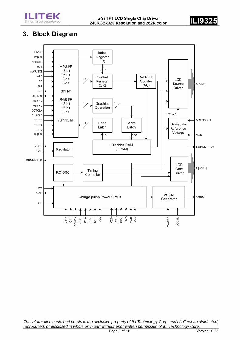
3. Block Diagram
MPU I/F18-bit16-bit9-bit8-bit
SPI I/F
RGB I/F18-bit16-bit6-bit
VSYNC I/F
nCSnWR/SCL
nRD
RS
DB[17:0]
SDI
SDO
VSYNC
HSYNC
TEST1
DOTCLK
nRESET
IM[3:0]
TEST2
TS[8:0]
IOVCC
RegulatorGND
RC-OSC. Timing Controller
Charge-pump Power Circuit
VREG1OUT
C11
+
VCI
C11
-
DD
VDH
C12
+
C12
-
VCL
C22
+
C22
-
VGH
VGL
VCOMGenerator VCOM
VCO
MH
VCO
ML
IndexRegister
(IR)
Control Register
(CR)
18
7
GraphicsOperation
18
ReadLatch
18
18
WriteLatch
Graphics RAM(GRAM)
7272
Address Counter
(AC)LCD
SourceDriver
GrayscaleReference
Voltage
V63 ~ 0
S[720:1]
LCDGateDriver
G[320:1]
VGS
VCI1
GND
VDDD
C13
+
C13
-
C21
+
C21
-ENABLE
TEST3
DUMMY1~15
DUMMY20~27
a-Si TFT LCD Single Chip Driver
240RGBx320 Resolution and 262K color ILI9325
The information contained herein is the exclusive property of ILI Technology Corp. and shall not be distributed, reproduced, or disclosed in whole or in part without prior written permission of ILI Technology Corp. Page 10 of 111 Version: 0.35
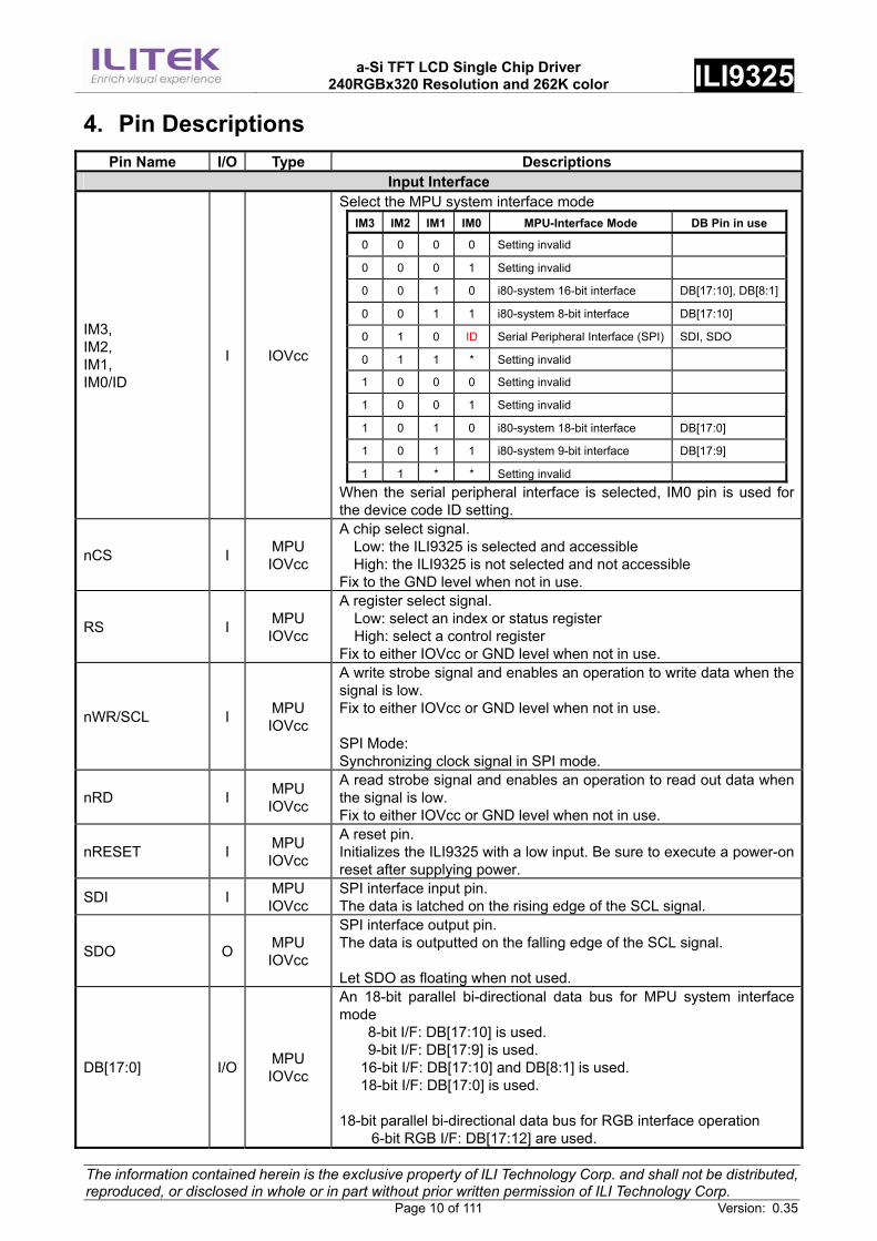
4. Pin Descriptions Pin Name I/O Type Descriptions
Input Interface
IM3, IM2, IM1, IM0/ID
I IOVcc
Select the MPU system interface mode IM3 IM2 IM1 IM0 MPU-Interface Mode DB Pin in use
0 0 0 0 Setting invalid
0 0 0 1 Setting invalid
0 0 1 0 i80-system 16-bit interface DB[17:10], DB[8:1]
0 0 1 1 i80-system 8-bit interface DB[17:10]
0 1 0 ID Serial Peripheral Interface (SPI) SDI, SDO
0 1 1 * Setting invalid
1 0 0 0 Setting invalid
1 0 0 1 Setting invalid
1 0 1 0 i80-system 18-bit interface DB[17:0]
1 0 1 1 i80-system 9-bit interface DB[17:9]
1 1 * * Setting invalid When the serial peripheral interface is selected, IM0 pin is used for the device code ID setting.
nCS I MPU IOVcc
A chip select signal. Low: the ILI9325 is selected and accessible High: the ILI9325 is not selected and not accessible
Fix to the GND level when not in use.
RS I MPU IOVcc
A register select signal. Low: select an index or status register High: select a control register Fix to either IOVcc or GND level when not in use.
nWR/SCL I MPU IOVcc
A write strobe signal and enables an operation to write data when the signal is low. Fix to either IOVcc or GND level when not in use. SPI Mode: Synchronizing clock signal in SPI mode.
nRD I MPU IOVcc
A read strobe signal and enables an operation to read out data when the signal is low. Fix to either IOVcc or GND level when not in use.
nRESET I MPU IOVcc
A reset pin. Initializes the ILI9325 with a low input. Be sure to execute a power-on reset after supplying power.
SDI I MPU IOVcc
SPI interface input pin. The data is latched on the rising edge of the SCL signal.
SDO O MPU IOVcc
SPI interface output pin. The data is outputted on the falling edge of the SCL signal. Let SDO as floating when not used.
DB[17:0] I/O MPU IOVcc
An 18-bit parallel bi-directional data bus for MPU system interface mode
8-bit I/F: DB[17:10] is used. 9-bit I/F: DB[17:9] is used.
16-bit I/F: DB[17:10] and DB[8:1] is used. 18-bit I/F: DB[17:0] is used.
18-bit parallel bi-directional data bus for RGB interface operation 6-bit RGB I/F: DB[17:12] are used.
a-Si TFT LCD Single Chip Driver
240RGBx320 Resolution and 262K color ILI9325
The information contained herein is the exclusive property of ILI Technology Corp. and shall not be distributed, reproduced, or disclosed in whole or in part without prior written permission of ILI Technology Corp. Page 11 of 111 Version: 0.35
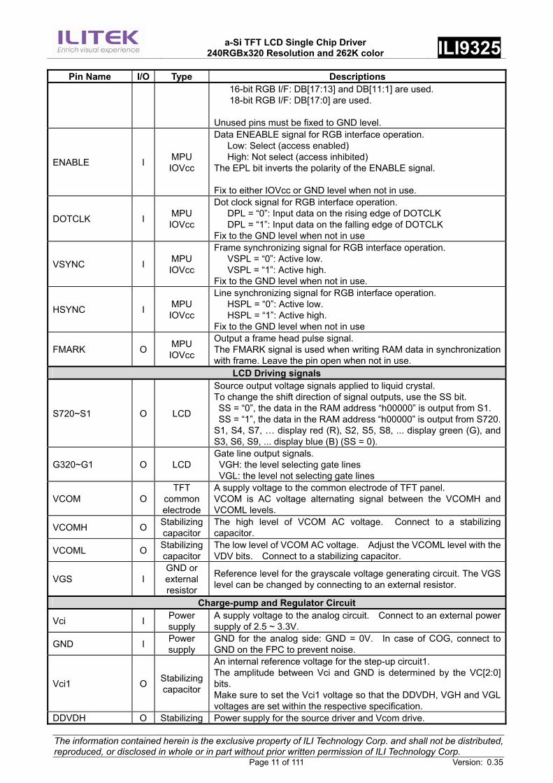
Pin Name I/O Type Descriptions 16-bit RGB I/F: DB[17:13] and DB[11:1] are used. 18-bit RGB I/F: DB[17:0] are used.
Unused pins must be fixed to GND level.
ENABLE I MPU IOVcc
Data ENEABLE signal for RGB interface operation. Low: Select (access enabled) High: Not select (access inhibited)
The EPL bit inverts the polarity of the ENABLE signal. Fix to either IOVcc or GND level when not in use.
DOTCLK I MPU IOVcc
Dot clock signal for RGB interface operation. DPL = “0”: Input data on the rising edge of DOTCLK DPL = “1”: Input data on the falling edge of DOTCLK
Fix to the GND level when not in use
VSYNC I MPU IOVcc
Frame synchronizing signal for RGB interface operation. VSPL = “0”: Active low. VSPL = “1”: Active high.
Fix to the GND level when not in use.
HSYNC I MPU IOVcc
Line synchronizing signal for RGB interface operation. HSPL = “0”: Active low. HSPL = “1”: Active high.
Fix to the GND level when not in use
FMARK O MPU IOVcc
Output a frame head pulse signal. The FMARK signal is used when writing RAM data in synchronization with frame. Leave the pin open when not in use.
LCD Driving signals
S720~S1 O LCD
Source output voltage signals applied to liquid crystal. To change the shift direction of signal outputs, use the SS bit. SS = “0”, the data in the RAM address “h00000” is output from S1. SS = “1”, the data in the RAM address “h00000” is output from S720.
S1, S4, S7, … display red (R), S2, S5, S8, ... display green (G), and S3, S6, S9, ... display blue (B) (SS = 0).
G320~G1 O LCD Gate line output signals. VGH: the level selecting gate lines VGL: the level not selecting gate lines
VCOM O TFT
common electrode
A supply voltage to the common electrode of TFT panel. VCOM is AC voltage alternating signal between the VCOMH and VCOML levels.
VCOMH O Stabilizing capacitor
The high level of VCOM AC voltage. Connect to a stabilizing capacitor.
VCOML O Stabilizing capacitor
The low level of VCOM AC voltage. Adjust the VCOML level with the VDV bits. Connect to a stabilizing capacitor.
VGS I GND or external resistor
Reference level for the grayscale voltage generating circuit. The VGS level can be changed by connecting to an external resistor.
Charge-pump and Regulator Circuit
Vci I Power supply
A supply voltage to the analog circuit. Connect to an external power supply of 2.5 ~ 3.3V.
GND I Power supply
GND for the analog side: GND = 0V. In case of COG, connect to GND on the FPC to prevent noise.
Vci1 O Stabilizing capacitor
An internal reference voltage for the step-up circuit1. The amplitude between Vci and GND is determined by the VC[2:0] bits. Make sure to set the Vci1 voltage so that the DDVDH, VGH and VGL voltages are set within the respective specification.
DDVDH O Stabilizing Power supply for the source driver and Vcom drive.
a-Si TFT LCD Single Chip Driver
240RGBx320 Resolution and 262K color ILI9325
The information contained herein is the exclusive property of ILI Technology Corp. and shall not be distributed, reproduced, or disclosed in whole or in part without prior written permission of ILI Technology Corp. Page 12 of 111 Version: 0.35
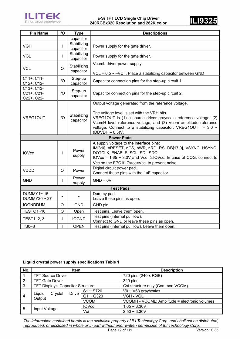
Pin Name I/O Type Descriptions capacitor
VGH I Stabilizing capacitor Power supply for the gate driver.
VGL I Stabilizing capacitor Power supply for the gate driver.
VCL O Stabilizing capacitor
VcomL driver power supply. VCL = 0.5 ~ –VCI . Place a stabilizing capacitor between GND
C11+, C11- C12+, C12- I/O Step-up
capacitor Capacitor connection pins for the step-up circuit 1.
C13+, C13- C21+, C21- C22+, C22-
I/O Step-up capacitor Capacitor connection pins for the step-up circuit 2.
VREG1OUT I/O Stabilizing capacitor
Output voltage generated from the reference voltage. The voltage level is set with the VRH bits. VREG1OUT is (1) a source driver grayscale reference voltage, (2) VcomH level reference voltage, and (3) Vcom amplitude reference voltage. Connect to a stabilizing capacitor. VREG1OUT = 3.0 ~ (DDVDH – 0.5)V.
Power Pads
IOVcc I Power supply
A supply voltage to the interface pins: IM[3:0], nRESET, nCS, nWR, nRD, RS, DB[17:0], VSYNC, HSYNC, DOTCLK, ENABLE, SCL, SDI, SDO. IOVcc = 1.65 ~ 3.3V and Vcc ≧IOVcc. In case of COG, connect to Vcc on the FPC if IOVcc=Vcc, to prevent noise.
VDDD O Power Digital circuit power pad. Connect these pins with the 1uF capacitor.
GND I Power supply GND = 0V.
Test Pads DUMMY1~ 15 DUMMY20 ~ 27 - - Dummy pad.
Leave these pins as open. IOGNDDUM O GND GND pin. TESTO1~16 O Open Test pins. Leave them open.
TEST1, 2, 3 I IOGND Test pins (internal pull low). Connect to GND or leave these pins as open.
TS0~8 I OPEN Test pins (internal pull low). Leave them open.
Liquid crystal power supply specifications Table 1
No. Item Description 1 TFT Source Driver 720 pins (240 x RGB) 2 TFT Gate Driver 320 pins 3 TFT Display’s Capacitor Structure Cst structure only (Common VCOM)
S1 ~ S720 V0 ~ V63 grayscales G1 ~ G320 VGH - VGL 4 Liquid Crystal Drive
Output VCOM VCOMH - VCOML: Amplitude = electronic volumes IOVcc 1.65 ~ 3.30V 5 Input Voltage Vci 2.50 ~ 3.30V
a-Si TFT LCD Single Chip Driver
240RGBx320 Resolution and 262K color ILI9325
The information contained herein is the exclusive property of ILI Technology Corp. and shall not be distributed, reproduced, or disclosed in whole or in part without prior written permission of ILI Technology Corp. Page 13 of 111 Version: 0.35
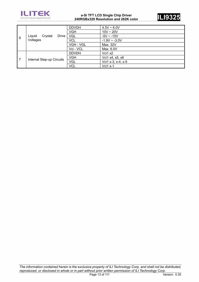
DDVDH 4.5V ~ 6.0V VGH 10V ~ 20V VGL -5V ~ -15V VCL -1.9V ~ -3.0V VGH - VGL Max. 32V
6 Liquid Crystal Drive Voltages
Vci - VCL Max. 6.0V DDVDH Vci1 x2 VGH Vci1 x4, x5, x6 VGL Vci1 x-3, x-4, x-5
7 Internal Step-up Circuits
VCL Vci1 x-1
a-Si TFT LCD Single Chip Driver
240RGBx320 Resolution and 262K color ILI9325
The information contained herein is the exclusive property of ILI Technology Corp. and shall not be distributed, reproduced, or disclosed in whole or in part without prior written permission of ILI Technology Corp. Page 14 of 111 Version: 0.35
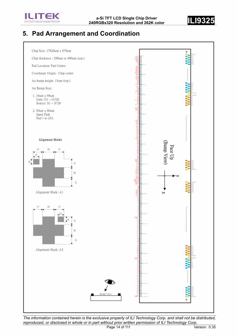
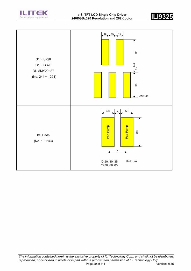
5. Pad Arrangement and Coordination
15 20 15
1520
15
Alignment Marks
Chip Size: 17820um x 870um
Chip thickness : 280um or 400um (typ.)
Pad Location: Pad Center.
Coordinate Origin: Chip center
Au bump height: 15um (typ.)
Au Bump Size:
1. 16um x 98um Gate: G1 ~ G320 Source: S1 ~ S720
2. 50um x 80um Input Pads Pad 1 to 243.
Bump View
10
10
Alignment Mark: A1
15 20 15
1520
15
10
10
Alignment Mark: A2
Face U
p
(Bum
p View
)
DUMMY23S361S362S363S364S365S366S367S368S369
x
y
S353S354S355S356S357S358S359S360DUMMY24
……
……
……
……
.
G304G306G308G310G312G314G316G318G320DUMMY20
DUMMY21G2G4G6G8G10G12G14G16G18
S712S713S714S715S716S717S718S719S720DUMMY22
……
……
DUMMY27G319G317G315G313G311G309G307G305G303
G17G15G13G11G9G7G5G3G1DUMMY26
DUMMY25S1S2S3S4S5S6S7S8S9
……
……
……
……
……
……
.
DUMMY1 TEST1
IOGNDDUMTESTO1 TESTO2 TESTO3
IM0/ID IM1 IM2 IM3
TEST2 TESTO4 TESTO5 TESTO6 TESTO7 TESTO8 TESTO9
TESTO10nRESET nRESET
VSYNC HSYNC
DOTCLK ENABLE
DB17 DB16 DB15 DB14 DB13
TESTO11
DB12 DB11 DB10
DB9 DB8
TEST3 TESTO12
DB7 DB6 DB5
DB4 DB3 DB2 DB1 DB0
TESTO13 SDO
SDI nRD
nWR/SCL
RS nCS
TESTO14TESTO15
FMARK TESTO16
TS8 TS7 TS6 TS5
TS4 TS3 TS2 TS1 TS0
DUMMY2IOVCCIOVCCIOVCCIOVCC
IOVCC IOVCC VDDDVDDDVDDDVDDDVDDDVDDDVDDDVDDD
VDDDVDDDVDDD
DUMMY3GND GND GND GND GND GND
GNDGNDVGS VGS GNDGNDGNDGNDGNDGND
GND GND GND GND
DUMMY4DUMMY5DUMMY6
VCOM VCOM VCOM
VCOM VCOM VCOM VCOM
VCOMH VCOMH VCOMH VCOMH VCOMH VCOMH
VCOML VCOML VCOML VCOML
VREG1OUTVREG1OUTVREG1OUT
DUMMY7DUMMY8DUMMY9
VCL VCL VCL VCL VCL
DDVDH DDVDH DDVDH DDVDH DDVDH
DDVDHVCI1 VCI1 VCI1
VCI VCI VCI VCI VCI VCI
VCIVCIVCIVCIVCIVCIVCIVCIVCIVCI
VCI VCI
DUMMY10DUMMY11
C12-C12-C12-C12-C12-C12+
C12+C12+C12+C12+C11-C11-C11-C11-C11-C11+
C11+C11+C11+C11+VGL VGL VGL VGL VGL VGL
VGL VGL VGL VGL GNDGNDGNDVGH VGH VGH
VGH VGH VGH
DUMMY12DUMMY13
C13-C13-C13-C13-C13+
C22-C22-C22-C22-C22+C22+C22+C22+C22+C22+
C13+C13+C13+C21-C21-C21-C21-C21-C21-C21-
C21+C21+C21+C21+C21+C21+C21+C22-C22-C22-
C22+DUMMY14DUMMY15
1
10
20
30
40
50
6070
80
90
100
110
120
130
140
150
160
170
180
190
200
210
220
230
240
243
a-Si TFT LCD Single Chip Driver
240RGBx320 Resolution and 262K color ILI9325
The information contained herein is the exclusive property of ILI Technology Corp. and shall not be distributed, reproduced, or disclosed in whole or in part without prior written permission of ILI Technology Corp. Page 15 of 111 Version: 0.35
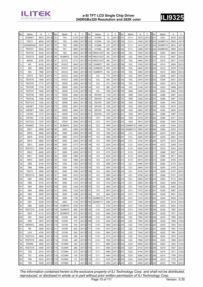
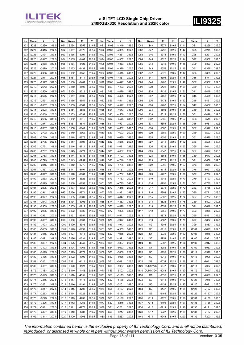
No. Name X Y No. Name X Y No. Name X Y No. Name X Y No. Name X Y 1 DUMMY1 -8610 -307.5 61 TS4 -4130 -307.5 121 VCOML 70 -307.5 181 C11+ 4270 -307.5 241 C22+ 8470 -307.5
2 TEST1 -8540 -307.5 62 TS3 -4060 -307.5 122 VCOML 140 -307.5 182 C11+ 4340 -307.5 242 DUMMY14 8540 -307.5
3 IOGNDDUM -8470 -307.5 63 TS2 -3990 -307.5 123 VCOML 210 -307.5 183 C11+ 4410 -307.5 243 DUMMY15 8610 -307.5
4 TESTO1 -8400 -307.5 64 TS1 -3920 -307.5 124 VCOML 280 -307.5 184 C11+ 4480 -307.5 244 DUMMY20 8659 202.5
5 TESTO2 -8330 -307.5 65 TS0 -3850 -307.5 125 VREG1OUT 350 -307.5 185 VGL 4550 -307.5 245 G320 8643 319.5
6 TESTO3 -8260 -307.5 66 DUMMY2 -3780 -307.5 126 VREG1OUT 420 -307.5 186 VGL 4620 -307.5 246 G318 8627 202.5
7 IM0/ID -8190 -307.5 67 IOVCC -3710 -307.5 127 VREG1OUT 490 -307.5 187 VGL 4690 -307.5 247 G316 8611 319.5
8 IM1 -8120 -307.5 68 IOVCC -3640 -307.5 128 DUMMY7 560 -307.5 188 VGL 4760 -307.5 248 G314 8595 202.5
9 IM2 -8050 -307.5 69 IOVCC -3570 -307.5 129 DUMMY8 630 -307.5 189 VGL 4830 -307.5 249 G312 8579 319.5
10 IM3 -7980 -307.5 70 IOVCC -3500 -307.5 130 DUMMY9 700 -307.5 190 VGL 4900 -307.5 250 G310 8563 202.5
11 TEST2 -7910 -307.5 71 IOVCC -3430 -307.5 131 VCL 770 -307.5 191 VGL 4970 -307.5 251 G308 8547 319.5
12 TESTO4 -7840 -307.5 72 IOVCC -3360 -307.5 132 VCL 840 -307.5 192 VGL 5040 -307.5 252 G306 8531 202.5
13 TESTO5 -7770 -307.5 73 VDDD -3290 -307.5 133 VCL 910 -307.5 193 VGL 5110 -307.5 253 G304 8515 319.5
14 TESTO6 -7700 -307.5 74 VDDD -3220 -307.5 134 VCL 980 -307.5 194 VGL 5180 -307.5 254 G302 8499 202.5
15 TESTO7 -7630 -307.5 75 VDDD -3150 -307.5 135 VCL 1050 -307.5 195 GND 5250 -307.5 255 G300 8483 319.5
16 TESTO8 -7560 -307.5 76 VDDD -3080 -307.5 136 DDVDH 1120 -307.5 196 GND 5320 -307.5 256 G298 8467 202.5
17 TESTO9 -7490 -307.5 77 VDDD -3010 -307.5 137 DDVDH 1190 -307.5 197 GND 5390 -307.5 257 G296 8451 319.5
18 TESTO10 -7420 -307.5 78 VDDD -2940 -307.5 138 DDVDH 1260 -307.5 198 VGH 5460 -307.5 258 G294 8435 202.5
19 nRESET -7350 -307.5 79 VDDD -2870 -307.5 139 DDVDH 1330 -307.5 199 VGH 5530 -307.5 259 G292 8419 319.5
20 nRESET -7280 -307.5 80 VDDD -2800 -307.5 140 DDVDH 1400 -307.5 200 VGH 5600 -307.5 260 G290 8403 202.5
21 VSYNC -7210 -307.5 81 VDDD -2730 -307.5 141 DDVDH 1470 -307.5 201 VGH 5670 -307.5 261 G288 8387 319.5
22 HSYNC -7140 -307.5 82 VDDD -2660 -307.5 142 VCI1 1540 -307.5 202 VGH 5740 -307.5 262 G286 8371 202.5
23 DOTCLK -7070 -307.5 83 VDDD -2590 -307.5 143 VCI1 1610 -307.5 203 VGH 5810 -307.5 263 G284 8355 319.5
24 ENABLE -7000 -307.5 84 DUMMY3 -2520 -307.5 144 VCI1 1680 -307.5 204 DUMMY12 5880 -307.5 264 G282 8339 202.5
25 DB17 -6905 -307.5 85 GND -2450 -307.5 145 VCI 1750 -307.5 205 DUMMY13 5950 -307.5 265 G280 8323 319.5
26 DB16 -6825 -307.5 86 GND -2380 -307.5 146 VCI 1820 -307.5 206 C13- 6020 -307.5 266 G278 8307 202.5
27 DB15 -6745 -307.5 87 GND -2310 -307.5 147 VCI 1890 -307.5 207 C13- 6090 -307.5 267 G276 8291 319.5
28 DB14 -6665 -307.5 88 GND -2240 -307.5 148 VCI 1960 -307.5 208 C13- 6160 -307.5 268 G274 8275 202.5
29 DB13 -6585 -307.5 89 GND -2170 -307.5 149 VCI 2030 -307.5 209 C13- 6230 -307.5 269 G272 8259 319.5
30 TESTO11 -6495 -307.5 90 GND -2100 -307.5 150 VCI 2100 -307.5 210 C13+ 6300 -307.5 270 G270 8243 202.5
31 DB12 -6405 -307.5 91 GND -2030 -307.5 151 VCI 2170 -307.5 211 C13+ 6370 -307.5 271 G268 8227 319.5
32 DB11 -6325 -307.5 92 GND -1960 -307.5 152 VCI 2240 -307.5 212 C13+ 6440 -307.5 272 G266 8211 202.5
33 DB10 -6245 -307.5 93 VGS -1890 -307.5 153 VCI 2310 -307.5 213 C13+ 6510 -307.5 273 G264 8195 319.5
34 DB9 -6165 -307.5 94 VGS -1820 -307.5 154 VCI 2380 -307.5 214 C21- 6580 -307.5 274 G262 8179 202.5
35 DB8 -6085 -307.5 95 GND -1750 -307.5 155 VCI 2450 -307.5 215 C21- 6650 -307.5 275 G260 8163 319.5
36 TEST3 -5990 -307.5 96 GND -1680 -307.5 156 VCI 2520 -307.5 216 C21- 6720 -307.5 276 G258 8147 202.5
37 TESTO12 -5920 -307.5 97 GND -1610 -307.5 157 VCI 2590 -307.5 217 C21- 6790 -307.5 277 G256 8131 319.5
38 DB7 -5825 -307.5 98 GND -1540 -307.5 158 VCI 2660 -307.5 218 C21- 6860 -307.5 278 G254 8115 202.5
39 DB6 -5745 -307.5 99 GND -1470 -307.5 159 VCI 2730 -307.5 219 C21- 6930 -307.5 279 G252 8099 319.5
40 DB5 -5665 -307.5 100 GND -1400 -307.5 160 VCI 2800 -307.5 220 C21- 7000 -307.5 280 G250 8083 202.5
41 DB4 -5585 -307.5 101 GND -1330 -307.5 161 VCI 2870 -307.5 221 C21+ 7070 -307.5 281 G248 8067 319.5
42 DB3 -5505 -307.5 102 GND -1260 -307.5 162 VCI 2940 -307.5 222 C21+ 7140 -307.5 282 G246 8051 202.5
43 DB2 -5425 -307.5 103 GND -1190 -307.5 163 DUMMY10 3010 -307.5 223 C21+ 7210 -307.5 283 G244 8035 319.5
44 DB1 -5345 -307.5 104 GND -1120 -307.5 164 DUMMY11 3080 -307.5 224 C21+ 7280 -307.5 284 G242 8019 202.5
45 DB0 -5265 -307.5 105 DUMMY4 -1050 -307.5 165 C12- 3150 -307.5 225 C21+ 7350 -307.5 285 G240 8003 319.5
46 TESTO13 -5180 -307.5 106 DUMMY5 -980 -307.5 166 C12- 3220 -307.5 226 C21+ 7420 -307.5 286 G238 7987 202.5
47 SDO -5110 -307.5 107 DUMMY6 -910 -307.5 167 C12- 3290 -307.5 227 C21+ 7490 -307.5 287 G236 7971 319.5
48 SDI -5040 -307.5 108 VCOM -840 -307.5 168 C12- 3360 -307.5 228 C22- 7560 -307.5 288 G234 7955 202.5
49 nRD -4970 -307.5 109 VCOM -770 -307.5 169 C12- 3430 -307.5 229 C22- 7630 -307.5 289 G232 7939 319.5
50 nWR/SCL -4900 -307.5 110 VCOM -700 -307.5 170 C12+ 3500 -307.5 230 C22- 7700 -307.5 290 G230 7923 202.5
51 RS -4830 -307.5 111 VCOM -630 -307.5 171 C12+ 3570 -307.5 231 C22- 7770 -307.5 291 G228 7907 319.5
52 nCS -4760 -307.5 112 VCOM -560 -307.5 172 C12+ 3640 -307.5 232 C22- 7840 -307.5 292 G226 7891 202.5
53 TESTO14 -4690 -307.5 113 VCOM -490 -307.5 173 C12+ 3710 -307.5 233 C22- 7910 -307.5 293 G224 7875 319.5
54 TESTO15 -4620 -307.5 114 VCOM -420 -307.5 174 C12+ 3780 -307.5 234 C22- 7980 -307.5 294 G222 7859 202.5
55 FMARK -4550 -307.5 115 VCOMH -350 -307.5 175 C11- 3850 -307.5 235 C22+ 8050 -307.5 295 G220 7843 319.5
56 TESTO16 -4480 -307.5 116 VCOMH -280 -307.5 176 C11- 3920 -307.5 236 C22+ 8120 -307.5 296 G218 7827 202.5
57 TS8 -4410 -307.5 117 VCOMH -210 -307.5 177 C11- 3990 -307.5 237 C22+ 8190 -307.5 297 G216 7811 319.5
58 TS7 -4340 -307.5 118 VCOMH -140 -307.5 178 C11- 4060 -307.5 238 C22+ 8260 -307.5 298 G214 7795 202.5
59 TS6 -4270 -307.5 119 VCOMH -70 -307.5 179 C11- 4130 -307.5 239 C22+ 8330 -307.5 299 G212 7779 319.5
60 TS5 -4200 -307.5 120 VCOMH 0 -307.5 180 C11+ 4200 -307.5 240 C22+ 8400 -307.5 300 G210 7763 202.5
a-Si TFT LCD Single Chip Driver
240RGBx320 Resolution and 262K color ILI9325
The information contained herein is the exclusive property of ILI Technology Corp. and shall not be distributed, reproduced, or disclosed in whole or in part without prior written permission of ILI Technology Corp. Page 16 of 111 Version: 0.35
No. Name X Y No. Name X Y No. Name X Y No. Name X Y No. Name X Y
301 G208 7747 319.5 361 G88 6787 319.5 421 S706 5807 202.5 481 S646 4847 202.5 541 S586 3887 202.5
302 G206 7731 202.5 362 G86 6771 202.5 422 S705 5791 319.5 482 S645 4831 319.5 542 S585 3871 319.5
303 G204 7715 319.5 363 G84 6755 319.5 423 S704 5775 202.5 483 S644 4815 202.5 543 S584 3855 202.5
304 G202 7699 202.5 364 G82 6739 202.5 424 S703 5759 319.5 484 S643 4799 319.5 544 S583 3839 319.5
305 G200 7683 319.5 365 G80 6723 319.5 425 S702 5743 202.5 485 S642 4783 202.5 545 S582 3823 202.5
306 G198 7667 202.5 366 G78 6707 202.5 426 S701 5727 319.5 486 S641 4767 319.5 546 S581 3807 319.5
307 G196 7651 319.5 367 G76 6691 319.5 427 S700 5711 202.5 487 S640 4751 202.5 547 S580 3791 202.5
308 G194 7635 202.5 368 G74 6675 202.5 428 S699 5695 319.5 488 S639 4735 319.5 548 S579 3775 319.5
309 G192 7619 319.5 369 G72 6659 319.5 429 S698 5679 202.5 489 S638 4719 202.5 549 S578 3759 202.5
310 G190 7603 202.5 370 G70 6643 202.5 430 S697 5663 319.5 490 S637 4703 319.5 550 S577 3743 319.5
311 G188 7587 319.5 371 G68 6627 319.5 431 S696 5647 202.5 491 S636 4687 202.5 551 S576 3727 202.5
312 G186 7571 202.5 372 G66 6611 202.5 432 S695 5631 319.5 492 S635 4671 319.5 552 S575 3711 319.5
313 G184 7555 319.5 373 G64 6595 319.5 433 S694 5615 202.5 493 S634 4655 202.5 553 S574 3695 202.5
314 G182 7539 202.5 374 G62 6579 202.5 434 S693 5599 319.5 494 S633 4639 319.5 554 S573 3679 319.5
315 G180 7523 319.5 375 G60 6563 319.5 435 S692 5583 202.5 495 S632 4623 202.5 555 S572 3663 202.5
316 G178 7507 202.5 376 G58 6547 202.5 436 S691 5567 319.5 496 S631 4607 319.5 556 S571 3647 319.5
317 G176 7491 319.5 377 G56 6531 319.5 437 S690 5551 202.5 497 S630 4591 202.5 557 S570 3631 202.5
318 G174 7475 202.5 378 G54 6515 202.5 438 S689 5535 319.5 498 S629 4575 319.5 558 S569 3615 319.5
319 G172 7459 319.5 379 G52 6499 319.5 439 S688 5519 202.5 499 S628 4559 202.5 559 S568 3599 202.5
320 G170 7443 202.5 380 G50 6483 202.5 440 S687 5503 319.5 500 S627 4543 319.5 560 S567 3583 319.5
321 G168 7427 319.5 381 G48 6467 319.5 441 S686 5487 202.5 501 S626 4527 202.5 561 S566 3567 202.5
322 G166 7411 202.5 382 G46 6451 202.5 442 S685 5471 319.5 502 S625 4511 319.5 562 S565 3551 319.5
323 G164 7395 319.5 383 G44 6435 319.5 443 S684 5455 202.5 503 S624 4495 202.5 563 S564 3535 202.5
324 G162 7379 202.5 384 G42 6419 202.5 444 S683 5439 319.5 504 S623 4479 319.5 564 S563 3519 319.5
325 G160 7363 319.5 385 G40 6403 319.5 445 S682 5423 202.5 505 S622 4463 202.5 565 S562 3503 202.5
326 G158 7347 202.5 386 G38 6387 202.5 446 S681 5407 319.5 506 S621 4447 319.5 566 S561 3487 319.5
327 G156 7331 319.5 387 G36 6371 319.5 447 S680 5391 202.5 507 S620 4431 202.5 567 S560 3471 202.5
328 G154 7315 202.5 388 G34 6355 202.5 448 S679 5375 319.5 508 S619 4415 319.5 568 S559 3455 319.5
329 G152 7299 319.5 389 G32 6339 319.5 449 S678 5359 202.5 509 S618 4399 202.5 569 S558 3439 202.5
330 G150 7283 202.5 390 G30 6323 202.5 450 S677 5343 319.5 510 S617 4383 319.5 570 S557 3423 319.5
331 G148 7267 319.5 391 G28 6307 319.5 451 S676 5327 202.5 511 S616 4367 202.5 571 S556 3407 202.5
332 G146 7251 202.5 392 G26 6291 202.5 452 S675 5311 319.5 512 S615 4351 319.5 572 S555 3391 319.5
333 G144 7235 319.5 393 G24 6275 319.5 453 S674 5295 202.5 513 S614 4335 202.5 573 S554 3375 202.5
334 G142 7219 202.5 394 G22 6259 202.5 454 S673 5279 319.5 514 S613 4319 319.5 574 S553 3359 319.5
335 G140 7203 319.5 395 G20 6243 319.5 455 S672 5263 202.5 515 S612 4303 202.5 575 S552 3343 202.5
336 G138 7187 202.5 396 G18 6227 202.5 456 S671 5247 319.5 516 S611 4287 319.5 576 S551 3327 319.5
337 G136 7171 319.5 397 G16 6211 319.5 457 S670 5231 202.5 517 S610 4271 202.5 577 S550 3311 202.5
338 G134 7155 202.5 398 G14 6195 202.5 458 S669 5215 319.5 518 S609 4255 319.5 578 S549 3295 319.5
339 G132 7139 319.5 399 G12 6179 319.5 459 S668 5199 202.5 519 S608 4239 202.5 579 S548 3279 202.5
340 G130 7123 202.5 400 G10 6163 202.5 460 S667 5183 319.5 520 S607 4223 319.5 580 S547 3263 319.5
341 G128 7107 319.5 401 G8 6147 319.5 461 S666 5167 202.5 521 S606 4207 202.5 581 S546 3247 202.5
342 G126 7091 202.5 402 G6 6131 202.5 462 S665 5151 319.5 522 S605 4191 319.5 582 S545 3231 319.5
343 G124 7075 319.5 403 G4 6115 319.5 463 S664 5135 202.5 523 S604 4175 202.5 583 S544 3215 202.5
344 G122 7059 202.5 404 G2 6099 202.5 464 S663 5119 319.5 524 S603 4159 319.5 584 S543 3199 319.5
345 G120 7043 319.5 405 DUMMY21 6083 319.5 465 S662 5103 202.5 525 S602 4143 202.5 585 S542 3183 202.5
346 G118 7027 202.5 406 DUMMY22 6047 319.5 466 S661 5087 319.5 526 S601 4127 319.5 586 S541 3167 319.5
347 G116 7011 319.5 407 S720 6031 202.5 467 S660 5071 202.5 527 S600 4111 202.5 587 S540 3151 202.5
348 G114 6995 202.5 408 S719 6015 319.5 468 S659 5055 319.5 528 S599 4095 319.5 588 S539 3135 319.5
349 G112 6979 319.5 409 S718 5999 202.5 469 S658 5039 202.5 529 S598 4079 202.5 589 S538 3119 202.5
350 G110 6963 202.5 410 S717 5983 319.5 470 S657 5023 319.5 530 S597 4063 319.5 590 S537 3103 319.5
351 G108 6947 319.5 411 S716 5967 202.5 471 S656 5007 202.5 531 S596 4047 202.5 591 S536 3087 202.5
352 G106 6931 202.5 412 S715 5951 319.5 472 S655 4991 319.5 532 S595 4031 319.5 592 S535 3071 319.5
353 G104 6915 319.5 413 S714 5935 202.5 473 S654 4975 202.5 533 S594 4015 202.5 593 S534 3055 202.5
354 G102 6899 202.5 414 S713 5919 319.5 474 S653 4959 319.5 534 S593 3999 319.5 594 S533 3039 319.5
355 G100 6883 319.5 415 S712 5903 202.5 475 S652 4943 202.5 535 S592 3983 202.5 595 S532 3023 202.5
356 G98 6867 202.5 416 S711 5887 319.5 476 S651 4927 319.5 536 S591 3967 319.5 596 S531 3007 319.5
357 G96 6851 319.5 417 S710 5871 202.5 477 S650 4911 202.5 537 S590 3951 202.5 597 S530 2991 202.5
358 G94 6835 202.5 418 S709 5855 319.5 478 S649 4895 319.5 538 S589 3935 319.5 598 S529 2975 319.5
359 G92 6819 319.5 419 S708 5839 202.5 479 S648 4879 202.5 539 S588 3919 202.5 599 S528 2959 202.5
360 G90 6803 202.5 420 S707 5823 319.5 480 S647 4863 319.5 540 S587 3903 319.5 600 S527 2943 319.5
a-Si TFT LCD Single Chip Driver
240RGBx320 Resolution and 262K color ILI9325
The information contained herein is the exclusive property of ILI Technology Corp. and shall not be distributed, reproduced, or disclosed in whole or in part without prior written permission of ILI Technology Corp. Page 17 of 111 Version: 0.35
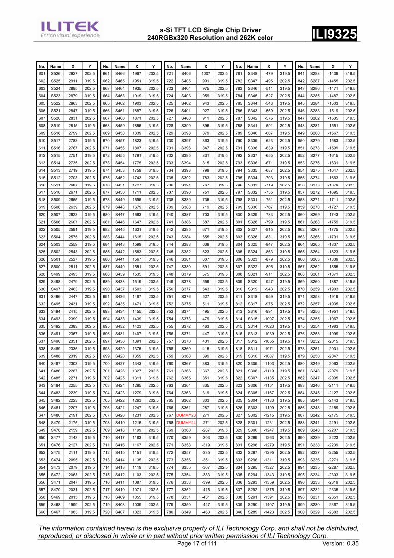
No. Name X Y No. Name X Y No. Name X Y No. Name X Y No. Name X Y
601 S526 2927 202.5 661 S466 1967 202.5 721 S406 1007 202.5 781 S348 -479 319.5 841 S288 -1439 319.5
602 S525 2911 319.5 662 S465 1951 319.5 722 S405 991 319.5 782 S347 -495 202.5 842 S287 -1455 202.5
603 S524 2895 202.5 663 S464 1935 202.5 723 S404 975 202.5 783 S346 -511 319.5 843 S286 -1471 319.5
604 S523 2879 319.5 664 S463 1919 319.5 724 S403 959 319.5 784 S345 -527 202.5 844 S285 -1487 202.5
605 S522 2863 202.5 665 S462 1903 202.5 725 S402 943 202.5 785 S344 -543 319.5 845 S284 -1503 319.5
606 S521 2847 319.5 666 S461 1887 319.5 726 S401 927 319.5 786 S343 -559 202.5 846 S283 -1519 202.5
607 S520 2831 202.5 667 S460 1871 202.5 727 S400 911 202.5 787 S342 -575 319.5 847 S282 -1535 319.5
608 S519 2815 319.5 668 S459 1855 319.5 728 S399 895 319.5 788 S341 -591 202.5 848 S281 -1551 202.5
609 S518 2799 202.5 669 S458 1839 202.5 729 S398 879 202.5 789 S340 -607 319.5 849 S280 -1567 319.5
610 S517 2783 319.5 670 S457 1823 319.5 730 S397 863 319.5 790 S339 -623 202.5 850 S279 -1583 202.5
611 S516 2767 202.5 671 S456 1807 202.5 731 S396 847 202.5 791 S338 -639 319.5 851 S278 -1599 319.5
612 S515 2751 319.5 672 S455 1791 319.5 732 S395 831 319.5 792 S337 -655 202.5 852 S277 -1615 202.5
613 S514 2735 202.5 673 S454 1775 202.5 733 S394 815 202.5 793 S336 -671 319.5 853 S276 -1631 319.5
614 S513 2719 319.5 674 S453 1759 319.5 734 S393 799 319.5 794 S335 -687 202.5 854 S275 -1647 202.5
615 S512 2703 202.5 675 S452 1743 202.5 735 S392 783 202.5 795 S334 -703 319.5 855 S274 -1663 319.5
616 S511 2687 319.5 676 S451 1727 319.5 736 S391 767 319.5 796 S333 -719 202.5 856 S273 -1679 202.5
617 S510 2671 202.5 677 S450 1711 202.5 737 S390 751 202.5 797 S332 -735 319.5 857 S272 -1695 319.5
618 S509 2655 319.5 678 S449 1695 319.5 738 S389 735 319.5 798 S331 -751 202.5 858 S271 -1711 202.5
619 S508 2639 202.5 679 S448 1679 202.5 739 S388 719 202.5 799 S330 -767 319.5 859 S270 -1727 319.5
620 S507 2623 319.5 680 S447 1663 319.5 740 S387 703 319.5 800 S329 -783 202.5 860 S269 -1743 202.5
621 S506 2607 202.5 681 S446 1647 202.5 741 S386 687 202.5 801 S328 -799 319.5 861 S268 -1759 319.5
622 S505 2591 319.5 682 S445 1631 319.5 742 S385 671 319.5 802 S327 -815 202.5 862 S267 -1775 202.5
623 S504 2575 202.5 683 S444 1615 202.5 743 S384 655 202.5 803 S326 -831 319.5 863 S266 -1791 319.5
624 S503 2559 319.5 684 S443 1599 319.5 744 S383 639 319.5 804 S325 -847 202.5 864 S265 -1807 202.5
625 S502 2543 202.5 685 S442 1583 202.5 745 S382 623 202.5 805 S324 -863 319.5 865 S264 -1823 319.5
626 S501 2527 319.5 686 S441 1567 319.5 746 S381 607 319.5 806 S323 -879 202.5 866 S263 -1839 202.5
627 S500 2511 202.5 687 S440 1551 202.5 747 S380 591 202.5 807 S322 -895 319.5 867 S262 -1855 319.5
628 S499 2495 319.5 688 S439 1535 319.5 748 S379 575 319.5 808 S321 -911 202.5 868 S261 -1871 202.5
629 S498 2479 202.5 689 S438 1519 202.5 749 S378 559 202.5 809 S320 -927 319.5 869 S260 -1887 319.5
630 S497 2463 319.5 690 S437 1503 319.5 750 S377 543 319.5 810 S319 -943 202.5 870 S259 -1903 202.5
631 S496 2447 202.5 691 S436 1487 202.5 751 S376 527 202.5 811 S318 -959 319.5 871 S258 -1919 319.5
632 S495 2431 319.5 692 S435 1471 319.5 752 S375 511 319.5 812 S317 -975 202.5 872 S257 -1935 202.5
633 S494 2415 202.5 693 S434 1455 202.5 753 S374 495 202.5 813 S316 -991 319.5 873 S256 -1951 319.5
634 S493 2399 319.5 694 S433 1439 319.5 754 S373 479 319.5 814 S315 -1007 202.5 874 S255 -1967 202.5
635 S492 2383 202.5 695 S432 1423 202.5 755 S372 463 202.5 815 S314 -1023 319.5 875 S254 -1983 319.5
636 S491 2367 319.5 696 S431 1407 319.5 756 S371 447 319.5 816 S313 -1039 202.5 876 S253 -1999 202.5
637 S490 2351 202.5 697 S430 1391 202.5 757 S370 431 202.5 817 S312 -1055 319.5 877 S252 -2015 319.5
638 S489 2335 319.5 698 S429 1375 319.5 758 S369 415 319.5 818 S311 -1071 202.5 878 S251 -2031 202.5
639 S488 2319 202.5 699 S428 1359 202.5 759 S368 399 202.5 819 S310 -1087 319.5 879 S250 -2047 319.5
640 S487 2303 319.5 700 S427 1343 319.5 760 S367 383 319.5 820 S309 -1103 202.5 880 S249 -2063 202.5
641 S486 2287 202.5 701 S426 1327 202.5 761 S366 367 202.5 821 S308 -1119 319.5 881 S248 -2079 319.5
642 S485 2271 319.5 702 S425 1311 319.5 762 S365 351 319.5 822 S307 -1135 202.5 882 S247 -2095 202.5
643 S484 2255 202.5 703 S424 1295 202.5 763 S364 335 202.5 823 S306 -1151 319.5 883 S246 -2111 319.5
644 S483 2239 319.5 704 S423 1279 319.5 764 S363 319 319.5 824 S305 -1167 202.5 884 S245 -2127 202.5
645 S482 2223 202.5 705 S422 1263 202.5 765 S362 303 202.5 825 S304 -1183 319.5 885 S244 -2143 319.5
646 S481 2207 319.5 706 S421 1247 319.5 766 S361 287 319.5 826 S303 -1199 202.5 886 S243 -2159 202.5
647 S480 2191 202.5 707 S420 1231 202.5 767 DUMMY23 271 202.5 827 S302 -1215 319.5 887 S242 -2175 319.5
648 S479 2175 319.5 708 S419 1215 319.5 768 DUMMY24 -271 202.5 828 S301 -1231 202.5 888 S241 -2191 202.5
649 S478 2159 202.5 709 S418 1199 202.5 769 S360 -287 319.5 829 S300 -1247 319.5 889 S240 -2207 319.5
650 S477 2143 319.5 710 S417 1183 319.5 770 S359 -303 202.5 830 S299 -1263 202.5 890 S239 -2223 202.5
651 S476 2127 202.5 711 S416 1167 202.5 771 S358 -319 319.5 831 S298 -1279 319.5 891 S238 -2239 319.5
652 S475 2111 319.5 712 S415 1151 319.5 772 S357 -335 202.5 832 S297 -1295 202.5 892 S237 -2255 202.5
653 S474 2095 202.5 713 S414 1135 202.5 773 S356 -351 319.5 833 S296 -1311 319.5 893 S236 -2271 319.5
654 S473 2079 319.5 714 S413 1119 319.5 774 S355 -367 202.5 834 S295 -1327 202.5 894 S235 -2287 202.5
655 S472 2063 202.5 715 S412 1103 202.5 775 S354 -383 319.5 835 S294 -1343 319.5 895 S234 -2303 319.5
656 S471 2047 319.5 716 S411 1087 319.5 776 S353 -399 202.5 836 S293 -1359 202.5 896 S233 -2319 202.5
657 S470 2031 202.5 717 S410 1071 202.5 777 S352 -415 319.5 837 S292 -1375 319.5 897 S232 -2335 319.5
658 S469 2015 319.5 718 S409 1055 319.5 778 S351 -431 202.5 838 S291 -1391 202.5 898 S231 -2351 202.5
659 S468 1999 202.5 719 S408 1039 202.5 779 S350 -447 319.5 839 S290 -1407 319.5 899 S230 -2367 319.5
660 S467 1983 319.5 720 S407 1023 319.5 780 S349 -463 202.5 840 S289 -1423 202.5 900 S229 -2383 202.5
a-Si TFT LCD Single Chip Driver
240RGBx320 Resolution and 262K color ILI9325
The information contained herein is the exclusive property of ILI Technology Corp. and shall not be distributed, reproduced, or disclosed in whole or in part without prior written permission of ILI Technology Corp. Page 18 of 111 Version: 0.35
No. Name X Y No. Name X Y No. Name X Y No. Name X Y No. Name X Y
901 S228 -2399 319.5 961 S168 -3359 319.5 1021 S108 -4319 319.5 1081 S48 -5279 319.5 1141 G21 -6259 202.5
902 S227 -2415 202.5 962 S167 -3375 202.5 1022 S107 -4335 202.5 1082 S47 -5295 202.5 1142 G23 -6275 319.5
903 S226 -2431 319.5 963 S166 -3391 319.5 1023 S106 -4351 319.5 1083 S46 -5311 319.5 1143 G25 -6291 202.5
904 S225 -2447 202.5 964 S165 -3407 202.5 1024 S105 -4367 202.5 1084 S45 -5327 202.5 1144 G27 -6307 319.5
905 S224 -2463 319.5 965 S164 -3423 319.5 1025 S104 -4383 319.5 1085 S44 -5343 319.5 1145 G29 -6323 202.5
906 S223 -2479 202.5 966 S163 -3439 202.5 1026 S103 -4399 202.5 1086 S43 -5359 202.5 1146 G31 -6339 319.5
907 S222 -2495 319.5 967 S162 -3455 319.5 1027 S102 -4415 319.5 1087 S42 -5375 319.5 1147 G33 -6355 202.5
908 S221 -2511 202.5 968 S161 -3471 202.5 1028 S101 -4431 202.5 1088 S41 -5391 202.5 1148 G35 -6371 319.5
909 S220 -2527 319.5 969 S160 -3487 319.5 1029 S100 -4447 319.5 1089 S40 -5407 319.5 1149 G37 -6387 202.5
910 S219 -2543 202.5 970 S159 -3503 202.5 1030 S99 -4463 202.5 1090 S39 -5423 202.5 1150 G39 -6403 319.5
911 S218 -2559 319.5 971 S158 -3519 319.5 1031 S98 -4479 319.5 1091 S38 -5439 319.5 1151 G41 -6419 202.5
912 S217 -2575 202.5 972 S157 -3535 202.5 1032 S97 -4495 202.5 1092 S37 -5455 202.5 1152 G43 -6435 319.5
913 S216 -2591 319.5 973 S156 -3551 319.5 1033 S96 -4511 319.5 1093 S36 -5471 319.5 1153 G45 -6451 202.5
914 S215 -2607 202.5 974 S155 -3567 202.5 1034 S95 -4527 202.5 1094 S35 -5487 202.5 1154 G47 -6467 319.5
915 S214 -2623 319.5 975 S154 -3583 319.5 1035 S94 -4543 319.5 1095 S34 -5503 319.5 1155 G49 -6483 202.5
916 S213 -2639 202.5 976 S153 -3599 202.5 1036 S93 -4559 202.5 1096 S33 -5519 202.5 1156 G51 -6499 319.5
917 S212 -2655 319.5 977 S152 -3615 319.5 1037 S92 -4575 319.5 1097 S32 -5535 319.5 1157 G53 -6515 202.5
918 S211 -2671 202.5 978 S151 -3631 202.5 1038 S91 -4591 202.5 1098 S31 -5551 202.5 1158 G55 -6531 319.5
919 S210 -2687 319.5 979 S150 -3647 319.5 1039 S90 -4607 319.5 1099 S30 -5567 319.5 1159 G57 -6547 202.5
920 S209 -2703 202.5 980 S149 -3663 202.5 1040 S89 -4623 202.5 1100 S29 -5583 202.5 1160 G59 -6563 319.5
921 S208 -2719 319.5 981 S148 -3679 319.5 1041 S88 -4639 319.5 1101 S28 -5599 319.5 1161 G61 -6579 202.5
922 S207 -2735 202.5 982 S147 -3695 202.5 1042 S87 -4655 202.5 1102 S27 -5615 202.5 1162 G63 -6595 319.5
923 S206 -2751 319.5 983 S146 -3711 319.5 1043 S86 -4671 319.5 1103 S26 -5631 319.5 1163 G65 -6611 202.5
924 S205 -2767 202.5 984 S145 -3727 202.5 1044 S85 -4687 202.5 1104 S25 -5647 202.5 1164 G67 -6627 319.5
925 S204 -2783 319.5 985 S144 -3743 319.5 1045 S84 -4703 319.5 1105 S24 -5663 319.5 1165 G69 -6643 202.5
926 S203 -2799 202.5 986 S143 -3759 202.5 1046 S83 -4719 202.5 1106 S23 -5679 202.5 1166 G71 -6659 319.5
927 S202 -2815 319.5 987 S142 -3775 319.5 1047 S82 -4735 319.5 1107 S22 -5695 319.5 1167 G73 -6675 202.5
928 S201 -2831 202.5 988 S141 -3791 202.5 1048 S81 -4751 202.5 1108 S21 -5711 202.5 1168 G75 -6691 319.5
929 S200 -2847 319.5 989 S140 -3807 319.5 1049 S80 -4767 319.5 1109 S20 -5727 319.5 1169 G77 -6707 202.5
930 S199 -2863 202.5 990 S139 -3823 202.5 1050 S79 -4783 202.5 1110 S19 -5743 202.5 1170 G79 -6723 319.5
931 S198 -2879 319.5 991 S138 -3839 319.5 1051 S78 -4799 319.5 1111 S18 -5759 319.5 1171 G81 -6739 202.5
932 S197 -2895 202.5 992 S137 -3855 202.5 1052 S77 -4815 202.5 1112 S17 -5775 202.5 1172 G83 -6755 319.5
933 S196 -2911 319.5 993 S136 -3871 319.5 1053 S76 -4831 319.5 1113 S16 -5791 319.5 1173 G85 -6771 202.5
934 S195 -2927 202.5 994 S135 -3887 202.5 1054 S75 -4847 202.5 1114 S15 -5807 202.5 1174 G87 -6787 319.5
935 S194 -2943 319.5 995 S134 -3903 319.5 1055 S74 -4863 319.5 1115 S14 -5823 319.5 1175 G89 -6803 202.5
936 S193 -2959 202.5 996 S133 -3919 202.5 1056 S73 -4879 202.5 1116 S13 -5839 202.5 1176 G91 -6819 319.5
937 S192 -2975 319.5 997 S132 -3935 319.5 1057 S72 -4895 319.5 1117 S12 -5855 319.5 1177 G93 -6835 202.5
938 S191 -2991 202.5 998 S131 -3951 202.5 1058 S71 -4911 202.5 1118 S11 -5871 202.5 1178 G95 -6851 319.5
939 S190 -3007 319.5 999 S130 -3967 319.5 1059 S70 -4927 319.5 1119 S10 -5887 319.5 1179 G97 -6867 202.5
940 S189 -3023 202.5 1000 S129 -3983 202.5 1060 S69 -4943 202.5 1120 S9 -5903 202.5 1180 G99 -6883 319.5
941 S188 -3039 319.5 1001 S128 -3999 319.5 1061 S68 -4959 319.5 1121 S8 -5919 319.5 1181 G101 -6899 202.5
942 S187 -3055 202.5 1002 S127 -4015 202.5 1062 S67 -4975 202.5 1122 S7 -5935 202.5 1182 G103 -6915 319.5
943 S186 -3071 319.5 1003 S126 -4031 319.5 1063 S66 -4991 319.5 1123 S6 -5951 319.5 1183 G105 -6931 202.5
944 S185 -3087 202.5 1004 S125 -4047 202.5 1064 S65 -5007 202.5 1124 S5 -5967 202.5 1184 G107 -6947 319.5
945 S184 -3103 319.5 1005 S124 -4063 319.5 1065 S64 -5023 319.5 1125 S4 -5983 319.5 1185 G109 -6963 202.5
946 S183 -3119 202.5 1006 S123 -4079 202.5 1066 S63 -5039 202.5 1126 S3 -5999 202.5 1186 G111 -6979 319.5
947 S182 -3135 319.5 1007 S122 -4095 319.5 1067 S62 -5055 319.5 1127 S2 -6015 319.5 1187 G113 -6995 202.5
948 S181 -3151 202.5 1008 S121 -4111 202.5 1068 S61 -5071 202.5 1128 S1 -6031 202.5 1188 G115 -7011 319.5
949 S180 -3167 319.5 1009 S120 -4127 319.5 1069 S60 -5087 319.5 1129 DUMMY25 -6047 319.5 1189 G117 -7027 202.5
950 S179 -3183 202.5 1010 S119 -4143 202.5 1070 S59 -5103 202.5 1130 DUMMY26 -6083 319.5 1190 G119 -7043 319.5
951 S178 -3199 319.5 1011 S118 -4159 319.5 1071 S58 -5119 319.5 1131 G1 -6099 202.5 1191 G121 -7059 202.5
952 S177 -3215 202.5 1012 S117 -4175 202.5 1072 S57 -5135 202.5 1132 G3 -6115 319.5 1192 G123 -7075 319.5
953 S176 -3231 319.5 1013 S116 -4191 319.5 1073 S56 -5151 319.5 1133 G5 -6131 202.5 1193 G125 -7091 202.5
954 S175 -3247 202.5 1014 S115 -4207 202.5 1074 S55 -5167 202.5 1134 G7 -6147 319.5 1194 G127 -7107 319.5
955 S174 -3263 319.5 1015 S114 -4223 319.5 1075 S54 -5183 319.5 1135 G9 -6163 202.5 1195 G129 -7123 202.5
956 S173 -3279 202.5 1016 S113 -4239 202.5 1076 S53 -5199 202.5 1136 G11 -6179 319.5 1196 G131 -7139 319.5
957 S172 -3295 319.5 1017 S112 -4255 319.5 1077 S52 -5215 319.5 1137 G13 -6195 202.5 1197 G133 -7155 202.5
958 S171 -3311 202.5 1018 S111 -4271 202.5 1078 S51 -5231 202.5 1138 G15 -6211 319.5 1198 G135 -7171 319.5
959 S170 -3327 319.5 1019 S110 -4287 319.5 1079 S50 -5247 319.5 1139 G17 -6227 202.5 1199 G137 -7187 202.5
960 S169 -3343 202.5 1020 S109 -4303 202.5 1080 S49 -5263 202.5 1140 G19 -6243 319.5 1200 G139 -7203 319.5
a-Si TFT LCD Single Chip Driver
240RGBx320 Resolution and 262K color ILI9325
The information contained herein is the exclusive property of ILI Technology Corp. and shall not be distributed, reproduced, or disclosed in whole or in part without prior written permission of ILI Technology Corp. Page 19 of 111 Version: 0.35
No. Name X Y No. Name X Y
1201 G141 -7219 202.5 1261 G261 -8179 202.5
1202 G143 -7235 319.5 1262 G263 -8195 319.5
1203 G145 -7251 202.5 1263 G265 -8211 202.5
1204 G147 -7267 319.5 1264 G267 -8227 319.5
1205 G149 -7283 202.5 1265 G269 -8243 202.5
1206 G151 -7299 319.5 1266 G271 -8259 319.5
1207 G153 -7315 202.5 1267 G273 -8275 202.5
1208 G155 -7331 319.5 1268 G275 -8291 319.5
1209 G157 -7347 202.5 1269 G277 -8307 202.5
1210 G159 -7363 319.5 1270 G279 -8323 319.5
1211 G161 -7379 202.5 1271 G281 -8339 202.5
1212 G163 -7395 319.5 1272 G283 -8355 319.5
1213 G165 -7411 202.5 1273 G285 -8371 202.5
1214 G167 -7427 319.5 1274 G287 -8387 319.5
1215 G169 -7443 202.5 1275 G289 -8403 202.5
1216 G171 -7459 319.5 1276 G291 -8419 319.5
1217 G173 -7475 202.5 1277 G293 -8435 202.5
1218 G175 -7491 319.5 1278 G295 -8451 319.5
1219 G177 -7507 202.5 1279 G297 -8467 202.5
1220 G179 -7523 319.5 1280 G299 -8483 319.5
1221 G181 -7539 202.5 1281 G301 -8499 202.5
1222 G183 -7555 319.5 1282 G303 -8515 319.5
1223 G185 -7571 202.5 1283 G305 -8531 202.5
1224 G187 -7587 319.5 1284 G307 -8547 319.5
1225 G189 -7603 202.5 1285 G309 -8563 202.5
1226 G191 -7619 319.5 1286 G311 -8579 319.5
1227 G193 -7635 202.5 1287 G313 -8595 202.5
1228 G195 -7651 319.5 1288 G315 -8611 319.5
1229 G197 -7667 202.5 1289 G317 -8627 202.5
1230 G199 -7683 319.5 1290 G319 -8643 319.5
1231 G201 -7699 202.5 1291 DUMMY27 -8659 202.5
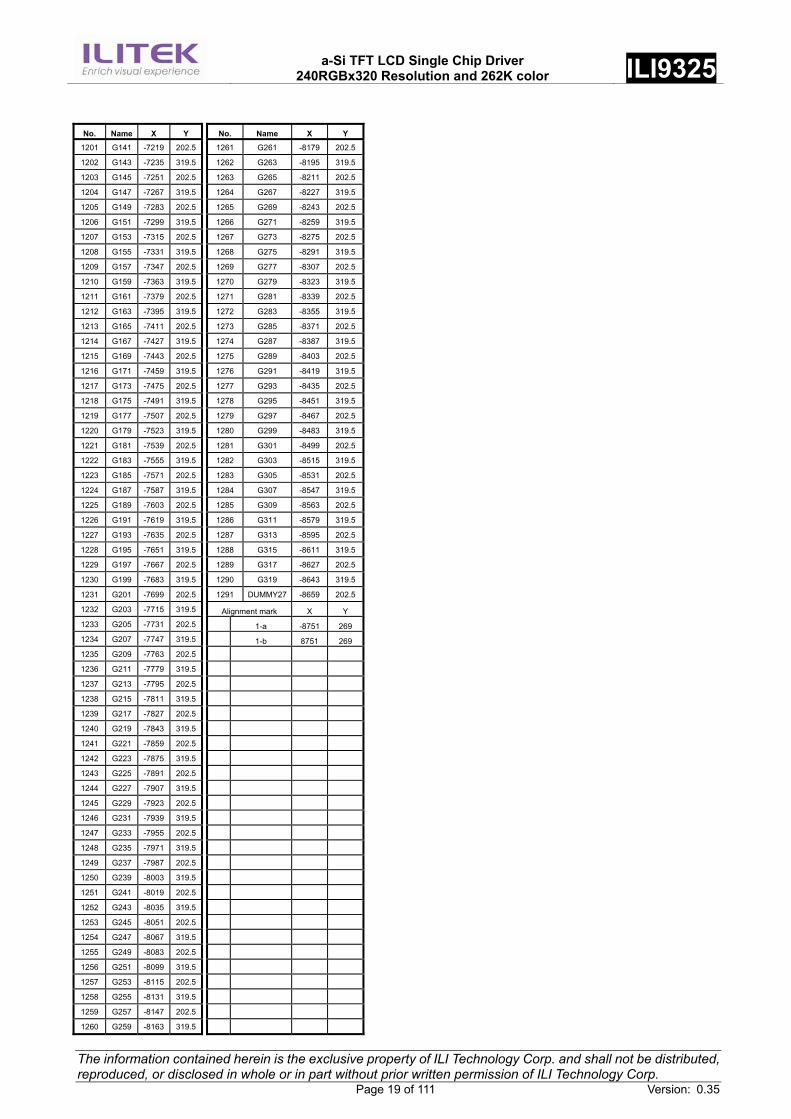
1232 G203 -7715 319.5 Alignment mark X Y 1233 G205 -7731 202.5 1-a -8751 269 1234 G207 -7747 319.5 1-b 8751 269 1235 G209 -7763 202.5 1236 G211 -7779 319.5 1237 G213 -7795 202.5 1238 G215 -7811 319.5 1239 G217 -7827 202.5 1240 G219 -7843 319.5 1241 G221 -7859 202.5 1242 G223 -7875 319.5 1243 G225 -7891 202.5 1244 G227 -7907 319.5 1245 G229 -7923 202.5 1246 G231 -7939 319.5 1247 G233 -7955 202.5 1248 G235 -7971 319.5 1249 G237 -7987 202.5 1250 G239 -8003 319.5 1251 G241 -8019 202.5 1252 G243 -8035 319.5 1253 G245 -8051 202.5 1254 G247 -8067 319.5 1255 G249 -8083 202.5 1256 G251 -8099 319.5 1257 G253 -8115 202.5 1258 G255 -8131 319.5 1259 G257 -8147 202.5 1260 G259 -8163 319.5
a-Si TFT LCD Single Chip Driver
240RGBx320 Resolution and 262K color ILI9325
The information contained herein is the exclusive property of ILI Technology Corp. and shall not be distributed, reproduced, or disclosed in whole or in part without prior written permission of ILI Technology Corp. Page 20 of 111 Version: 0.35
S1 ~ S720
G1 ~ G320
DUMMY20~27
(No. 244 ~ 1291)
16 16
9819
98
Unit: um
16
I/O Pads
(No. 1 ~ 243)
Pad
Pum
p
80
50 x
Pad
Pum
p
50
y
X=20, 30, 35Y=70, 80, 85
Unit: um
a-Si TFT LCD Single Chip Driver
240RGBx320 Resolution and 262K color ILI9325
The information contained herein is the exclusive property of ILI Technology Corp. and shall not be distributed, reproduced, or disclosed in whole or in part without prior written permission of ILI Technology Corp. Page 21 of 111 Version: 0.35
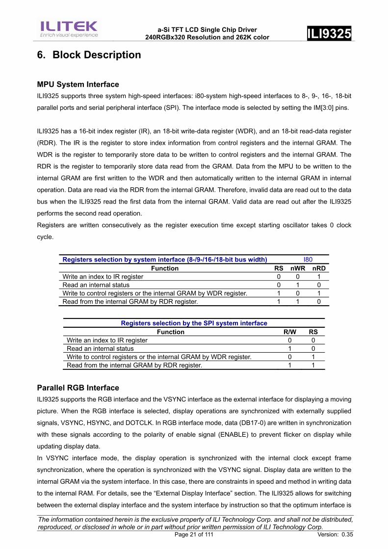
6. Block Description
MPU System Interface ILI9325 supports three system high-speed interfaces: i80-system high-speed interfaces to 8-, 9-, 16-, 18-bit
parallel ports and serial peripheral interface (SPI). The interface mode is selected by setting the IM[3:0] pins.
ILI9325 has a 16-bit index register (IR), an 18-bit write-data register (WDR), and an 18-bit read-data register
(RDR). The IR is the register to store index information from control registers and the internal GRAM. The
WDR is the register to temporarily store data to be written to control registers and the internal GRAM. The
RDR is the register to temporarily store data read from the GRAM. Data from the MPU to be written to the
internal GRAM are first written to the WDR and then automatically written to the internal GRAM in internal
operation. Data are read via the RDR from the internal GRAM. Therefore, invalid data are read out to the data
bus when the ILI9325 read the first data from the internal GRAM. Valid data are read out after the ILI9325
performs the second read operation.
Registers are written consecutively as the register execution time except starting oscillator takes 0 clock
cycle.
Registers selection by system interface (8-/9-/16-/18-bit bus width) I80 Function RS nWR nRD
Write an index to IR register 0 0 1 Read an internal status 0 1 0 Write to control registers or the internal GRAM by WDR register. 1 0 1 Read from the internal GRAM by RDR register. 1 1 0
Registers selection by the SPI system interface Function R/W RS
Write an index to IR register 0 0 Read an internal status 1 0 Write to control registers or the internal GRAM by WDR register. 0 1 Read from the internal GRAM by RDR register. 1 1
Parallel RGB Interface
ILI9325 supports the RGB interface and the VSYNC interface as the external interface for displaying a moving
picture. When the RGB interface is selected, display operations are synchronized with externally supplied
signals, VSYNC, HSYNC, and DOTCLK. In RGB interface mode, data (DB17-0) are written in synchronization
with these signals according to the polarity of enable signal (ENABLE) to prevent flicker on display while
updating display data.
In VSYNC interface mode, the display operation is synchronized with the internal clock except frame
synchronization, where the operation is synchronized with the VSYNC signal. Display data are written to the
internal GRAM via the system interface. In this case, there are constraints in speed and method in writing data
to the internal RAM. For details, see the “External Display Interface” section. The ILI9325 allows for switching
between the external display interface and the system interface by instruction so that the optimum interface is
a-Si TFT LCD Single Chip Driver
240RGBx320 Resolution and 262K color ILI9325
The information contained herein is the exclusive property of ILI Technology Corp. and shall not be distributed, reproduced, or disclosed in whole or in part without prior written permission of ILI Technology Corp. Page 22 of 111 Version: 0.35
selected for the kind of picture to be displayed on the screen (still and/or moving picture(s)). The RGB
interface, by writing all display data to the internal RAM, allows for transferring data only when updating the
frames of a moving picture, contributing to low power requirement for moving picture display.
Bit Operation
The ILI9325 supports a write data mask function for selectively writing data to the internal RAM in units of bits
and a logical/compare operation to write data to the GRAM only when a condition is met as a result of
comparing the data and the compare register bits. For details, see “Graphics Operation Functions”.
Address Counter (AC) The address counter (AC) gives an address to the internal GRAM. When the index of the register for setting a
RAM address in the AC is written to the IR, the address information is sent from the IR to the AC. As writing
data to the internal GRAM, the address in the AC is automatically updated plus or minus 1. The window
address function enables writing data only in the rectangular area arbitrarily set by users on the GRAM.
Graphics RAM (GRAM) GRAM is graphics RAM storing bit-pattern data of 172,820 (240 x 320x 18/8) bytes with 18 bits per pixel.
Grayscale Voltage Generating Circuit The grayscale voltage generating circuit generates a liquid crystal drive voltage according to grayscale data
set in the γ-correction register to display in 262,144 colors. For details, see the “γ-Correction Register”
section.
Timing Controller
The timing generator generates a timing signal for operation of internal circuits such as the internal GRAM.
The timing for the display operation such as RAM read operation and the timing for the internal operation such
as access from the MPU are generated in the way not to interfere each other.
Oscillator (OSC) ILI9325 generates RC oscillation with an internal oscillation resistor. The frame rate is adjusted by the register
setting.
LCD Driver Circuit
The LCD driver circuit of ILI9325 consists of a 720-output source driver (S1 ~ S720) and a 320-output gate
driver (G1~G320). Display pattern data are latched when the 720th bit data are input. The latched data control
the source driver and generate a drive waveform. The gate driver for scanning gate lines outputs either VGH
or VGL level. The shift direction of 720 source outputs from the source driver is set with the SS bit and the
shift direction of gate outputs from the gate driver is set with the GS bit. The scan mode by the gate driver is
a-Si TFT LCD Single Chip Driver
240RGBx320 Resolution and 262K color ILI9325
The information contained herein is the exclusive property of ILI Technology Corp. and shall not be distributed, reproduced, or disclosed in whole or in part without prior written permission of ILI Technology Corp. Page 23 of 111 Version: 0.35
set with the SM bit. These bits allow setting an appropriate scan method for an LCD module.
LCD Driver Power Supply Circuit The LCD drive power supply circuit generates the voltage levels VREG1OUT, VGH, VGL and Vcom for
driving an LCD.
a-Si TFT LCD Single Chip Driver
240RGBx320 Resolution and 262K color ILI9325
The information contained herein is the exclusive property of ILI Technology Corp. and shall not be distributed, reproduced, or disclosed in whole or in part without prior written permission of ILI Technology Corp. Page 24 of 111 Version: 0.35
7. System Interface
7.1. Interface Specifications ILI9325 has the system interface to read/write the control registers and display graphics memory (GRAM),
and the RGB Input Interface for displaying a moving picture. User can select an optimum interface to display
the moving or still picture with efficient data transfer. All display data are stored in the GRAM to reduce the
data transfer efforts and only the updating data is necessary to be transferred. User can only update a
sub-range of GRAM by using the window address function.
ILI9325 also has the RGB interface and VSYNC interface to transfer the display data without flicker the
moving picture on the screen. In RGB interface mode, the display data is written into the GRAM through the
control signals of ENABLE, VSYNC, HSYNC, DOTCLK and data bus DB[17:0].
In VSYNC interface mode, the internal display timing is synchronized with the frame synchronization signal
(VSYNC). The VSYNC interface mode enables to display the moving picture display through the system
interface. In this case, there are some constraints of speed and method to write data to the internal RAM.
ILI9325 operates in one of the following 4 modes. The display mode can be switched by the control register.
When switching from one mode to another, refer to the sequences mentioned in the sections of RGB and
VSYNC interfaces.
Operation Mode RAM Access Setting (RM)
Display Operation Mode (DM[1:0])
Internal operating clock only (Displaying still pictures)
System interface (RM = 0)
Internal operating clock (DM[1:0] = 00)
RGB interface (1) (Displaying moving pictures)
RGB interface (RM = 1)
RGB interface (DM[1:0] = 01)
RGB interface (2) (Rewriting still pictures while displaying moving pictures)
System interface (RM = 0)
RGB interface (DM[1:0] = 01)
VSYNC interface (Displaying moving pictures)
System interface (RM = 0)
VSYNC interface (DM[1:0] = 01)
Note 1) Registers are set only via the system interface.
Note 2) The RGB-I/F and the VSYNC-I/F are not available simultaneously.
a-Si TFT LCD Single Chip Driver
240RGBx320 Resolution and 262K color ILI9325
The information contained herein is the exclusive property of ILI Technology Corp. and shall not be distributed, reproduced, or disclosed in whole or in part without prior written permission of ILI Technology Corp. Page 25 of 111 Version: 0.35
SystemInterface
RGBInterface
ILI9325
nCSRSnWRnRDDB[17:0]
ENABLEVSYNCHSYNCDOTCLK
18/16/6System
Figure1 System Interface and RGB Interface connection
7.2. Input Interfaces The following are the system interfaces available with the ILI9325. The interface is selected by setting the
IM[3:0] pins. The system interface is used for setting registers and GRAM access.
IM3 IM2 IM1 IM0/ID Interface Mode DB Pin 0 0 0 0 Setting invalid 0 0 0 1 Setting invalid 0 0 1 0 i80-system 16-bit interface DB[17:10], DB[8:1] 0 0 1 1 i80-system 8-bit interface DB[17:10] 0 1 0 ID Serial Peripheral Interface (SPI) SDI, SDO (DB[1:0]) 0 1 1 * Setting invalid 1 0 0 0 Setting invalid 1 0 0 1 Setting invalid 1 0 1 0 i80-system18-bit interface DB[17:0] 1 0 1 1 i80-system 9-bit interface DB[17:9] 1 1 * * Setting invalid
a-Si TFT LCD Single Chip Driver
240RGBx320 Resolution and 262K color ILI9325
The information contained herein is the exclusive property of ILI Technology Corp. and shall not be distributed, reproduced, or disclosed in whole or in part without prior written permission of ILI Technology Corp. Page 26 of 111 Version: 0.35
7.2.1. i80/18-bit System Interface The i80/18-bit system interface is selected by setting the IM[3:0] as “1010” levels.
DB17
DB16
DB15
DB14
DB13
DB12
DB11
DB10
DB9
DB8
DB7
DB6
DB5
DB4
DB3
DB2
DB1
DB0
18-bit System Interface (262K colors) TRI=0, DFM[1:0]=00
Input Data
Write Data Register
R5 R4 R3 R2 R1 R0 G5 G4 G2 G1 G0 B5 B4 B3 B2 B1G3GRAM Data & RGB Mapping B0
WD17
WD16
WD15
WD14
WD13
WD12
WD11
WD10
WD9
WD8
WD7
WD6
WD5
WD4
WD3
WD2
WD1
WD0
nCSRSnWRnRDDB[17:0]
18
SystemnCS
A2nWRnRD
D[31:0]
Figure2 18-bit System Interface Data Format
a-Si TFT LCD Single Chip Driver
240RGBx320 Resolution and 262K color ILI9325
The information contained herein is the exclusive property of ILI Technology Corp. and shall not be distributed, reproduced, or disclosed in whole or in part without prior written permission of ILI Technology Corp. Page 27 of 111 Version: 0.35
7.2.2. i80/16-bit System Interface The i80/16-bit system interface is selected by setting the IM[3:0] as “0010” levels. The 262K or 65K color can
be display through the 16-bit MPU interface. When the 262K color is displayed, two transfers (1st transfer: 2
bits, 2nd transfer: 16 bits or 1st transfer: 16 bits, 2nd transfer: 2 bits) are necessary for the 16-bit CPU interface.
TRI DFM 16-bit MPU System Interface Data Format
R4R5 R2R3 R0R1 G4G5 G2G3 G0G1 B4B5 B2B3 B0B1
0 *
system 16-bit interface (1 transfers/pixel) 65,536 colors
R4R5 R2R3 R0R1 G4G5 G2G3 G0G1 B4B5 B2B3 B0B1
1 0
80-system 16-bit interface (2 transfers/pixel) 262,144 colors
R4R5 R2R3 R0R1 G4G5 G2G3 G0G1 B4B5 B2B3 B0B1
1 1
80-system 16-bit interface (2 transfers/pixel) 262,144 colors
DB16
DB17
DB14
DB15
DB12
DB13
DB10
DB11
DB7
DB8
DB5
DB6
DB3
DB4
DB1
DB2
1st Transfer
DB16
DB17
DB14
DB15
DB12
DB13
DB10
DB11
DB7
DB8
DB5
DB6
DB3
DB4
DB1
DB2
1st TransferDB16
DB17
2nd Transfer
DB16
DB17
DB14
DB15
DB12
DB13
DB10
DB11
DB7
DB8
DB5
DB6
DB3
DB4
DB1
DB2
2nd Transfer1st TransferDB1
DB2
Figure3 16-bit System Interface Data Format
a-Si TFT LCD Single Chip Driver
240RGBx320 Resolution and 262K color ILI9325
The information contained herein is the exclusive property of ILI Technology Corp. and shall not be distributed, reproduced, or disclosed in whole or in part without prior written permission of ILI Technology Corp. Page 28 of 111 Version: 0.35
7.2.3. i80/9-bit System Interface The i80/9-bit system interface is selected by setting the IM[3:0] as “1011” and the DB17~DB9 pins are used to
transfer the data. When writing the 16-bit register, the data is divided into upper byte (8 bits and LSB is not
used) lower byte and the upper byte is transferred first. The display data is also divided in upper byte (9 bits)
and lower byte, and the upper byte is transferred first. The unused DB[8:0] pins must be tied to GND.
nCSRSnWRnRDDB[17:9]
9
SystemnCS
A1nWRnRD
D[8:0]
1st Transfer (Upper bits)DB17
DB16
DB15
DB14
DB13
DB12
DB11
DB10
DB9
9-bit System Interface (262K colors) TRI=0, DFM[1:0]=00
Input Data
Write Data Register
R5 R4 R3 R2 R1 R0 G5 G4 G2 G1 G0 B5 B4 B3 B2 B1G3GRAM Data & RGB Mapping B0
WD17
WD16
WD15
WD14
WD13
WD12
WD11
WD10
WD9
WD8
WD7
WD6
WD5
WD4
WD3
WD2
WD1
WD0
DB17
DB16
DB15
DB14
DB13
DB12
DB11
DB10
DB9
2nd Transfer (Lower bits)
Figure4 9-bit System Interface Data Format
7.2.4. i80/8-bit System Interface The i80/8-bit system interface is selected by setting the IM[3:0] as “0011” and the DB17~DB10 pins are used
to transfer the data. When writing the 16-bit register, the data is divided into upper byte (8 bits and LSB is not
used) lower byte and the upper byte is transferred first. The display data is also divided in upper byte (8 bits)
and lower byte, and the upper byte is transferred first. The written data is expanded into 18 bits internally (see
the figure below) and then written into GRAM. The unused DB[9:0] pins must be tied to GND.
a-Si TFT LCD Single Chip Driver
240RGBx320 Resolution and 262K color ILI9325
The information contained herein is the exclusive property of ILI Technology Corp. and shall not be distributed, reproduced, or disclosed in whole or in part without prior written permission of ILI Technology Corp. Page 29 of 111 Version: 0.35
TRI DFM 8-bit MPU System Interface Data Format
DB16
DB17
DB14
DB15
DB12
DB13
DB10
DB11
DB16
DB17
DB14
DB15
DB12
DB13
DB10
DB11
R4R5 R2R3 R0R1 G4G5 G2G3 G0G1 B4B5 B2B3 B0B1
1st Transfer 2nd Transfer0 *
system 8-bit interface (2 transfers/pixel) 65,536 colors
DB16
DB17
DB14
DB15
DB12
DB13
DB10
DB11
DB16
DB17
DB14
DB15
DB12
DB13
DB10
DB11
R4R5 R2R3 R0R1 G4G5 G2G3 G0G1 B4B5 B2B3 B0B1
2nd Transfer 3rd Transfer1 0
80-system 8-bit interface (3 transfers/pixel) 262,144 colors
DB10
DB11
1st Transfer
R4R5 R2R3 R0R1 G4G5 G2G3 G0G1 B4B5 B2B3 B0B1
1 1
80-system 8-bit interface (3 transfers/pixel) 262,144 colors
DB16
DB17
DB14
DB15
DB12
DB13
DB16
DB17
DB14
DB15
DB12
DB13
2nd Transfer 3rd Transfer1st TransferDB16
DB17
DB14
DB15
DB12
DB13
Figure5 8-bit System Interface Data Format
Data transfer synchronization in 8/9-bit bus interface mode
ILI9325 supports a data transfer synchronization function to reset upper and lower counters which count the
transfers numbers of upper and lower byte in 8/9-bit interface mode. If a mismatch arises in the numbers of
transfers between the upper and lower byte counters due to noise and so on, the “00”h register is written 4
times consecutively to reset the upper and lower counters so that data transfer will restart with a transfer of
upper byte. This synchronization function can effectively prevent display error if the upper/lower counters are
periodically reset.
“00”hUpper/Lower “00”h “00”h “00”h Upper LowerDB[17:9]
RS
RD
nWR
8-/9-bit transfersynchronization
Figure6 Data Transfer Synchronization in 8/9-bit System Interface
7.3. Serial Peripheral Interface (SPI) The Serial Peripheral Interface (SPI) is selected by setting the IM[3:0] pins as “010x” level. The chip select pin
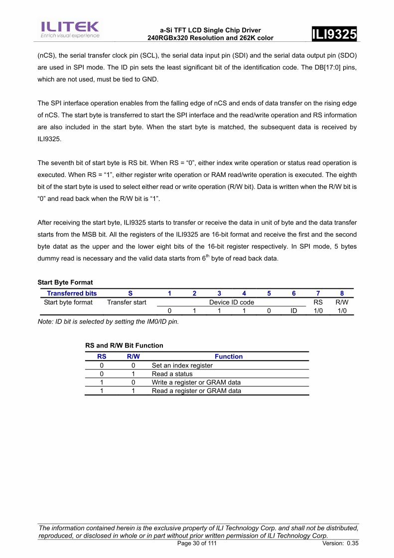
a-Si TFT LCD Single Chip Driver
240RGBx320 Resolution and 262K color ILI9325
The information contained herein is the exclusive property of ILI Technology Corp. and shall not be distributed, reproduced, or disclosed in whole or in part without prior written permission of ILI Technology Corp. Page 30 of 111 Version: 0.35
(nCS), the serial transfer clock pin (SCL), the serial data input pin (SDI) and the serial data output pin (SDO)
are used in SPI mode. The ID pin sets the least significant bit of the identification code. The DB[17:0] pins,
which are not used, must be tied to GND.
The SPI interface operation enables from the falling edge of nCS and ends of data transfer on the rising edge
of nCS. The start byte is transferred to start the SPI interface and the read/write operation and RS information
are also included in the start byte. When the start byte is matched, the subsequent data is received by
ILI9325.
The seventh bit of start byte is RS bit. When RS = “0”, either index write operation or status read operation is
executed. When RS = “1”, either register write operation or RAM read/write operation is executed. The eighth
bit of the start byte is used to select either read or write operation (R/W bit). Data is written when the R/W bit is
“0” and read back when the R/W bit is “1”.
After receiving the start byte, ILI9325 starts to transfer or receive the data in unit of byte and the data transfer
starts from the MSB bit. All the registers of the ILI9325 are 16-bit format and receive the first and the second
byte datat as the upper and the lower eight bits of the 16-bit register respectively. In SPI mode, 5 bytes
dummy read is necessary and the valid data starts from 6th byte of read back data.
Start Byte Format Transferred bits S 1 2 3 4 5 6 7 8
Start byte format Transfer start Device ID code RS R/W 0 1 1 1 0 ID 1/0 1/0
Note: ID bit is selected by setting the IM0/ID pin.
RS and R/W Bit Function RS R/W Function 0 0 Set an index register 0 1 Read a status 1 0 Write a register or GRAM data 1 1 Read a register or GRAM data
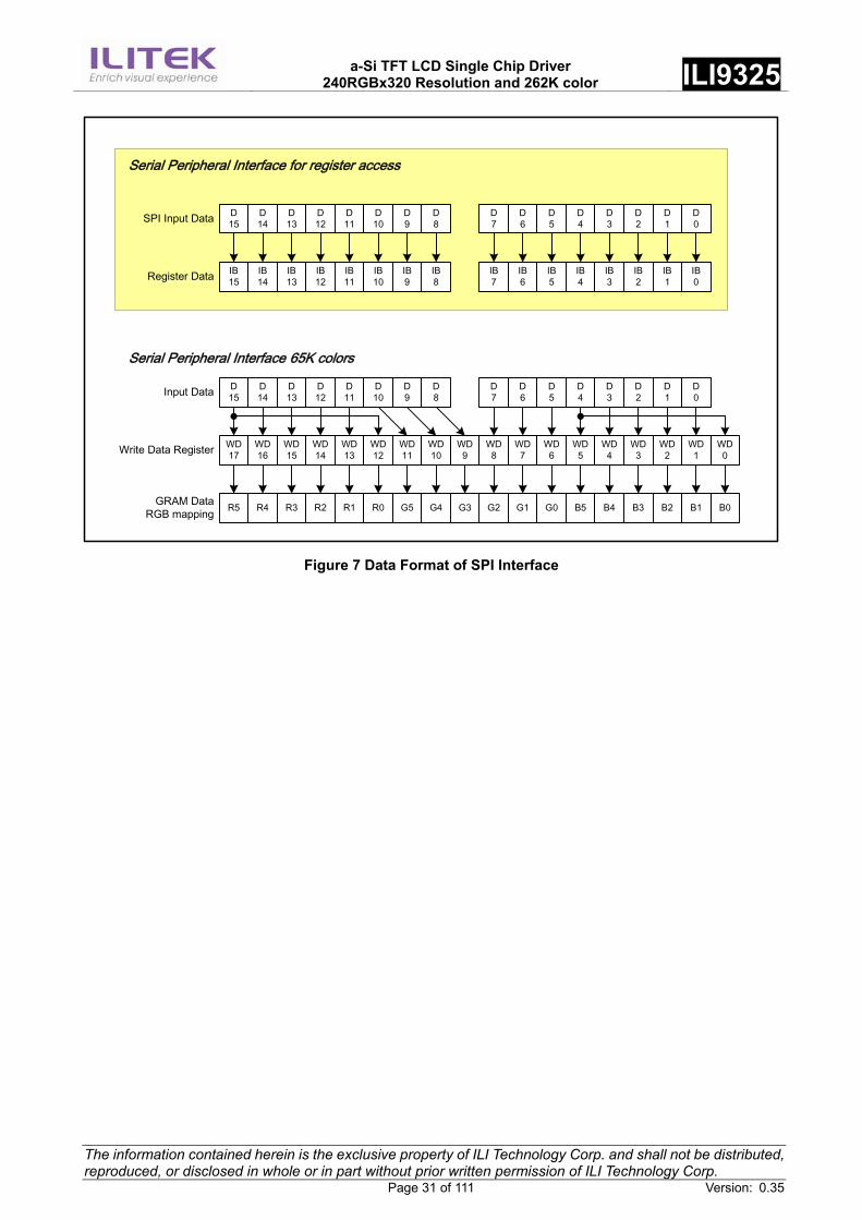
a-Si TFT LCD Single Chip Driver
240RGBx320 Resolution and 262K color ILI9325
The information contained herein is the exclusive property of ILI Technology Corp. and shall not be distributed, reproduced, or disclosed in whole or in part without prior written permission of ILI Technology Corp. Page 31 of 111 Version: 0.35
WD17
WD16
WD15
WD14
WD13
WD12
WD11
WD10
WD9
WD8
WD7
WD6
WD5
WD4
WD3
WD2
WD1
WD0
Serial Peripheral Interface 65K colors
Input Data
GRAM DataRGB mapping R5 R4 R3 R2 R1 R0 G5 G4 G2 G1 G0 B5 B4 B3 B2 B1G3 B0
D15
D14
D13
D12
D11
D10
D9
D8
D7
D6
D5
D4
D3
D2
D1
D0
Write Data Register
Serial Peripheral Interface for register access
SPI Input Data D15
D14
D13
D12
D11
D10
D8
D7
D6
D5
D4
D3
D2
D1
Register Data IB15
IB14
IB13
IB12
IB11
IB10
IB8
IB7
IB6
IB5
IB4
IB3
IB2
IB1
D9
IB9
D0
IB0
Figure 7 Data Format of SPI Interface
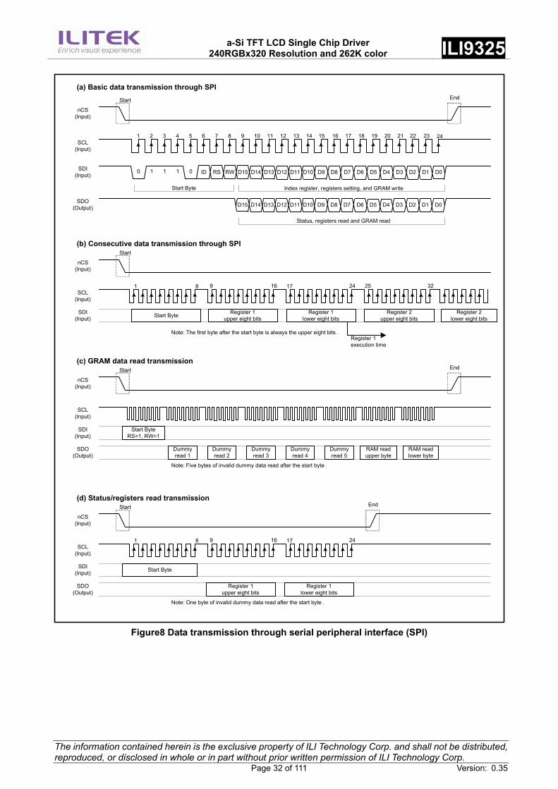
a-Si TFT LCD Single Chip Driver
240RGBx320 Resolution and 262K color ILI9325
The information contained herein is the exclusive property of ILI Technology Corp. and shall not be distributed, reproduced, or disclosed in whole or in part without prior written permission of ILI Technology Corp. Page 32 of 111 Version: 0.35
1 2 3 4 5 6 7 8 9 10 11 12 13 14 15 16 17 18 19 20 21 22 23 24
0 1 1 1 0 ID RS RW D15 D14 D13 D12 D11 D10 D9 D8 D7 D6 D5 D4 D3 D2 D1 D0
Start Byte Index register, registers setting, and GRAM write
D15 D14 D13 D12 D11 D10 D9 D8 D7 D6 D5 D4 D3 D2 D1 D0
Status, registers read and GRAM read
Start
SCL(Input)
SDI(Input)
SDO(Output)
(a) Basic data transmission through SPIEnd
nCS(Input)
1 8 16 24 329 17 25
Start
nCS(Input)
(b) Consecutive data transmission through SPI
Start Byte Register 1upper eight bits
Register 1lower eight bits
Register 2upper eight bits
SDI(Input)
SCL(Input)
Register 1 execution time
Note: The first byte after the start byte is always the upper eight bits .
Start End
nCS(Input)
(c) GRAM data read transmission
SDI(Input)
SCL(Input)
Dummy read 1
Dummy read 2
Dummy read 3
Dummy read 4
Dummy read 5
RAM read upper byte
RAM read lower byte
SDO(Output)
Note: Five bytes of invalid dummy data read after the start byte .
Start End
nCS(Input)
(d) Status/registers read transmission
Start ByteSDI(Input)
SCL(Input)
SDO(Output)
Note: One byte of invalid dummy data read after the start byte .
Start ByteRS=1, RW=1
1 8 16 249 17
Register 1upper eight bits
Register 1lower eight bits
Register 2lower eight bits
Figure8 Data transmission through serial peripheral interface (SPI)
a-Si TFT LCD Single Chip Driver
240RGBx320 Resolution and 262K color ILI9325
The information contained herein is the exclusive property of ILI Technology Corp. and shall not be distributed, reproduced, or disclosed in whole or in part without prior written permission of ILI Technology Corp. Page 33 of 111 Version: 0.35
1 2 3 4 5 6 7 8 9 10 11 12 13 14 15 16 17 18 19 20 21 22 23 24
0 1 1 1 0 ID RS RW D15 D14 D13 D12 D11 D10 D9 D8 D7 D6 D5 D4 D3 D2 D1 D0
Start Byte GRAM data write
GRAM data read
Start
SCL(Input)
SDI(Input)
SDO(Output)
(e) Basic data transmission through SPIEnd
nCS(Input)
Start End
nCS(Input)
(f) GRAM data write transmission
SDI(Input)
SCL(Input)
SDO(Output)
Note: Five bytes of invalid dummy data read after the start byte.
Start Byte
25 26 27 28 29 30 31 32
D16D17D18D19D120D21D22D23
D15 D14 D13 D12 D11 D10 D9 D8 D7 D6 D5 D4 D3 D2 D1 D0D16D17D18D19D120D21D22D23
Start End
nCS(Input)
(g) GRAM data read transmission
SDI(Input)
SCL(Input)
Dummyread 1
Dummyread 2
Dummyread 3
Dummyread 4
Dummyread 5
RAM read1st byte
RAM read2nd byte
SDO(Output)
Note: Five bytes of invalid dummy data read after the start byte.
Start ByteRS=1, RW=1
RAM data 11st transfer
RAM data 12nd transfer
RAM data 13rd transfer
RAM data 21st transfer
RAM data 22nd transfer
RAM data 23rd transfer
RAM read3rd byte
RAM data transfer in SPI mode when TRI=1 and DFM[1:0]=10.
GRAM Data (1)execution time
GRAM Data (2)execution time
Figure9 Data transmission through serial peripheral interface (SPI), TRI=”1” and DFM=”10”)
a-Si TFT LCD Single Chip Driver
240RGBx320 Resolution and 262K color ILI9325
The information contained herein is the exclusive property of ILI Technology Corp. and shall not be distributed, reproduced, or disclosed in whole or in part without prior written permission of ILI Technology Corp. Page 34 of 111 Version: 0.35
7.4. VSYNC Interface ILI9325 supports the VSYNC interface in synchronization with the frame-synchronizing signal VSYNC to
display the moving picture with the i80 system interface. When the VSYNC interface is selected to display a
moving picture, the minimum GRAM update speed is limited and the VSYNC interface is enabled by setting
DM[1:0] = “10” and RM = “0”.
MPU
VSYNC
nCSRS
DB[17:0]nWR
Figure10 Data transmission through VSYNC interface)
In the VSYNC mode, the display operation is synchronized with the internal clock and VSYNC input and the
frame rate is determined by the pulse rate of VSYNC signal. All display data are stored in GRAM to minimize
total data transfer required for moving picture display.
Rewritingscreen data
Rewritingscreen data
VSYNC
Write data to RAMthrough system
interface
Display operationsynchronized with
internal clocks
Figure11 Moving picture data transmission through VSYNC interface
a-Si TFT LCD Single Chip Driver
240RGBx320 Resolution and 262K color ILI9325
The information contained herein is the exclusive property of ILI Technology Corp. and shall not be distributed, reproduced, or disclosed in whole or in part without prior written permission of ILI Technology Corp. Page 35 of 111 Version: 0.35
Display(320 lines)
Back porch (14 lines)
Front porch (2 lines)
Black period
VSYNC RAMWrite
Display operation
Figure12 Operation through VSYNC Interface
The VSYNC interface has the minimum speed limitation of writing data to the internal GRAM via the system
interface, which are calculated from the following formula.
Internal clock frequency (fosc.) [Hz] = FrameFrequency x (DisplayLine (NL) + FrontPorch (FP) + BackPorch
(BP)) x ClockCyclePerLines (RTN) x FrequencyFluctuation.
Minimum RAM write speed (HZ)320 x DisplayLines (NL)
[(BackPorch(BP)+DisplayLines(NL) - margins] x 16 (clocks) x 1/fosc
Note: When the RAM write operation does not start from the falling edge of VSYNC, the time from the falling
edge of VSYNC until the start of RAM write operation must also be taken into account.
An example of minimum GRAM writing speed and internal clock frequency in VSYNC interface mode is as
below.
[Example]
Display size: 240 RGB × 320 lines
Lines: 320 lines (NL = 1000111)
Back porch: 14 lines (BP = 1110)
Front porch: 2 lines (FP = 0010)
Frame frequency: 60 Hz
Frequency fluctuation: 10%
Internal oscillator clock (fosc.) [Hz] = 60 x [320+ 2 + 14] x 16 clocks x (1.1/0.9) ≒ 394KHz
a-Si TFT LCD Single Chip Driver
240RGBx320 Resolution and 262K color ILI9325
The information contained herein is the exclusive property of ILI Technology Corp. and shall not be distributed, reproduced, or disclosed in whole or in part without prior written permission of ILI Technology Corp. Page 36 of 111 Version: 0.35
When calculate the internal clock frequency, the oscillator variation is needed to be taken into consideration.
In the above example, the calculated internal clock frequency with ±10% margin variation is considered and
ensures to complete the display operation within one VSYNC cycle. The causes of frequency variation come
from fabrication process of LSI, room temperature, external resistors and VCI voltage variation.
Minimum speed for RAM writing [Hz] > 240 x 320 x 394K / [ (14 + 320 – 2)lines x 16clocks] ≒ 5.7 MHz
The above theoretical value is calculated based on the premise that the ILI9325 starts to write data into the
internal GRAM on the falling edge of VSYNC. There must at least be a margin of 2 lines between the physical
display line and the GRAM line address where data writing operation is performed. The GRAM write speed of
5.7MHz or more will guarantee the completion of GRAM write operation before the ILI9325 starts to display
the GRAM data on the screen and enable to rewrite the entire screen without flicker.
Notes in using the VSYNC interface
1. The minimum GRAM write speed must be satisfied and the frequency variation must be taken into
consideration.
2. The display frame rate is determined by the VSYNC signal and the period of VSYNC must be longer than
the scan period of an entire display.
3. When switching from the internal clock operation mode (DM[1:0] = “00”) to the VSYNC interface mode or
inversely, the switching starts from the next VSYNC cycle, i.e. after completing the display of the frame.
4. The partial display, vertical scroll, and interlaced scan functions are not available in VSYNC interface mode
and set the AM bit to “0” to transfer display data.
a-Si TFT LCD Single Chip Driver
240RGBx320 Resolution and 262K color ILI9325
The information contained herein is the exclusive property of ILI Technology Corp. and shall not be distributed, reproduced, or disclosed in whole or in part without prior written permission of ILI Technology Corp. Page 37 of 111 Version: 0.35
Set HWM=1, AM=0
Set GRAM Address
Set DM[1:0]=10, RM=0for VSYNC interface mode
Set index register to R22h
Write data to GRAMthrough VSYNC interface
Wait more than 1 frame
System Interface Mode to VSYNC interface mode
System Interface
Opeartion through VSYNC interface
Display operation in synchronization with internal clocks
DM[1:0], RM become enable after completion of displaying 1 frame
Display operation in synchronization with VSYNC
Set DM[1:0]=00, RM=0for system interface mode
Wait more than 1 frame
VSYNC interface mode to System Interface Mode
System Interface
Opeartion through VSYNC interface
Display operation in synchronization with internal clocks
Display operation in synchronization with VSYNC
DM[1:0], RM become enable after completion of displaying 1 frame
Note: input VSYNC for more than 1 frame period after setting the DM, RM register.
Figure13 Transition flow between VSYNC and internal clock operation modes
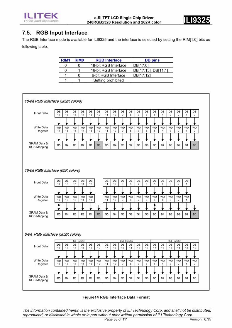
a-Si TFT LCD Single Chip Driver
240RGBx320 Resolution and 262K color ILI9325
The information contained herein is the exclusive property of ILI Technology Corp. and shall not be distributed, reproduced, or disclosed in whole or in part without prior written permission of ILI Technology Corp. Page 38 of 111 Version: 0.35
7.5. RGB Input Interface The RGB Interface mode is available for ILI9325 and the interface is selected by setting the RIM[1:0] bits as
following table.
RIM1 RIM0 RGB Interface DB pins 0 0 18-bit RGB Interface DB[17:0] 0 1 16-bit RGB Interface DB[17:13], DB[11:1] 1 0 6-bit RGB Interface DB[17:12] 1 1 Setting prohibited
18-bit RGB Interface (262K colors)
Input Data
Write Data Register
R5 R4 R3 R2 R1 R0 G5 G4 G2 G1 G0 B5 B4 B3 B2 B1G3GRAM Data & RGB Mapping B0
WD17
WD16
WD15
WD14
WD13
WD12
WD11
WD10
WD9
WD8
WD7
WD6
WD5
WD4
WD3
WD2
WD1
WD0
DB17
DB16
DB15
DB14
DB13
DB12
6-bit RGB Interface (262K colors)
Input Data
Write Data Register
R5 R4 R3 R2 R1 R0 G5 G4 G2 G1 G0 B5 B4 B3 B2 B1G3GRAM Data & RGB Mapping B0
WD17
WD16
WD15
WD14
WD13
WD12
WD11
WD10
WD9
WD8
WD7
WD6
WD5
WD4
WD3
WD2
WD1
WD0
DB17
DB16
DB15
DB14
DB13
DB12
1st Transfer 2nd TransferDB17
DB16
DB15
DB14
DB13
DB12
3rd Transfer
DB17
DB16
DB15
DB14
DB13
DB12
DB11
DB10
DB9
DB8
DB7
DB6
DB5
DB4
DB3
DB2
DB1
DB0
16-bit RGB Interface (65K colors)
Input Data
Write Data Register
R5 R4 R3 R2 R1 R0 G5 G4 G2 G1 G0 B5 B4 B3 B2 B1G3GRAM Data & RGB Mapping B0
WD17
WD16
WD15
WD14
WD13
WD11
WD10
WD9
WD8
WD7
WD6
WD5
WD4
WD3
WD2
WD1
DB17
DB16
DB15
DB14
DB13
DB11
DB10
DB9
DB8
DB7
DB6
DB5
DB4
DB3
DB2
DB1
Figure14 RGB Interface Data Format
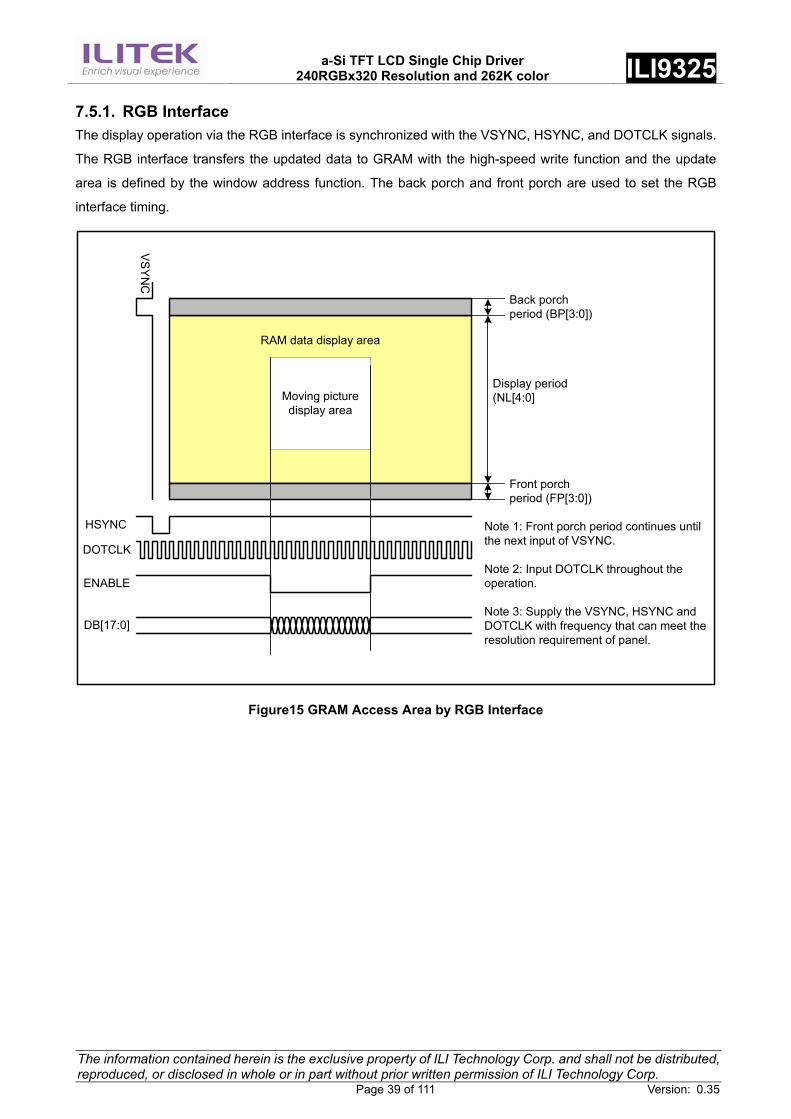
a-Si TFT LCD Single Chip Driver
240RGBx320 Resolution and 262K color ILI9325
The information contained herein is the exclusive property of ILI Technology Corp. and shall not be distributed, reproduced, or disclosed in whole or in part without prior written permission of ILI Technology Corp. Page 39 of 111 Version: 0.35
7.5.1. RGB Interface The display operation via the RGB interface is synchronized with the VSYNC, HSYNC, and DOTCLK signals.
The RGB interface transfers the updated data to GRAM with the high-speed write function and the update
area is defined by the window address function. The back porch and front porch are used to set the RGB
interface timing.
VS
YN
C
HSYNC
DOTCLK
Moving picturedisplay area
ENABLE
RAM data display area
Back porchperiod (BP[3:0])
Display period(NL[4:0]
Front porchperiod (FP[3:0])
DB[17:0]
Note 1: Front porch period continues untilthe next input of VSYNC.
Note 2: Input DOTCLK throughout theoperation.
Note 3: Supply the VSYNC, HSYNC andDOTCLK with frequency that can meet theresolution requirement of panel.
Figure15 GRAM Access Area by RGB Interface
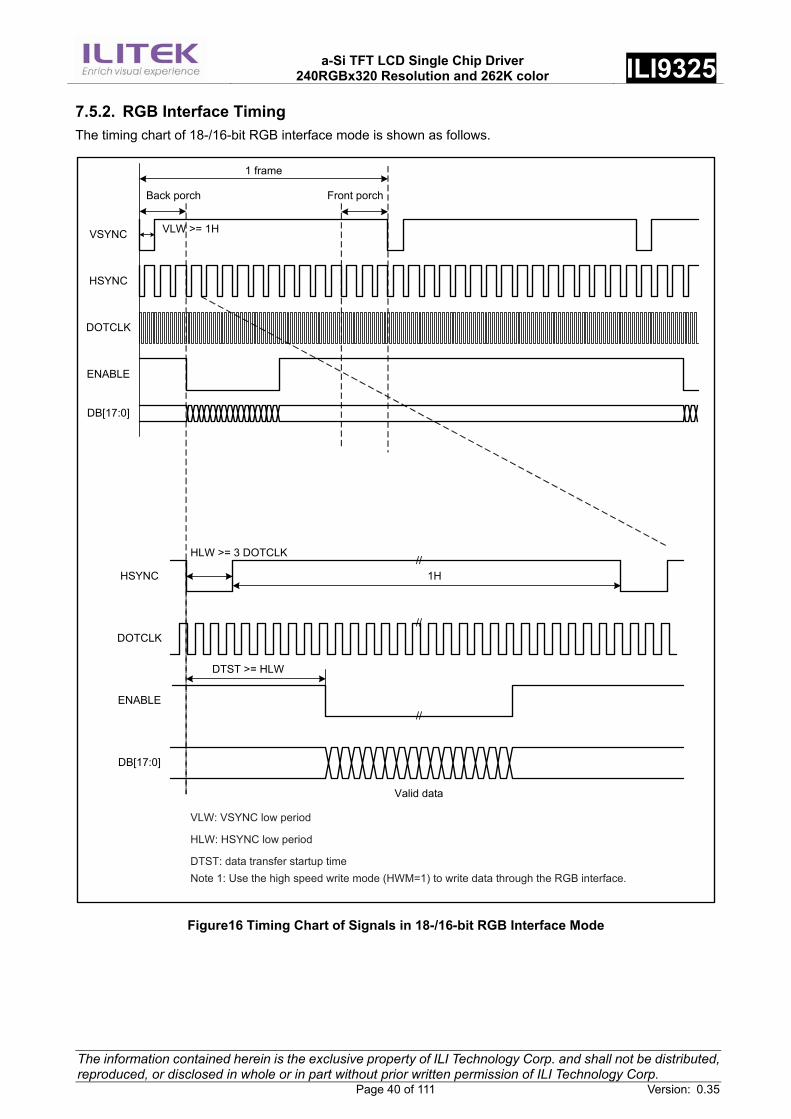
a-Si TFT LCD Single Chip Driver
240RGBx320 Resolution and 262K color ILI9325
The information contained herein is the exclusive property of ILI Technology Corp. and shall not be distributed, reproduced, or disclosed in whole or in part without prior written permission of ILI Technology Corp. Page 40 of 111 Version: 0.35
7.5.2. RGB Interface Timing The timing chart of 18-/16-bit RGB interface mode is shown as follows.
HSYNC
VSYNC
DOTCLK
ENABLE
DB[17:0]
Back porch Front porch
1 frame
VLW >= 1H
HLW >= 3 DOTCLK
HSYNC
DOTCLK
ENABLE
//
//
//
1H
DB[17:0]
DTST >= HLW
Valid data
VLW: VSYNC low period
HLW: HSYNC low period
DTST: data transfer startup timeNote 1: Use the high speed write mode (HWM=1) to write data through the RGB interface.
Figure16 Timing Chart of Signals in 18-/16-bit RGB Interface Mode
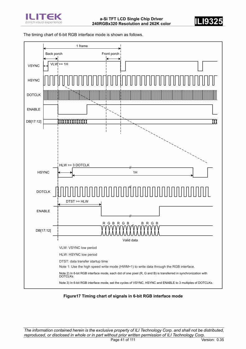
a-Si TFT LCD Single Chip Driver
240RGBx320 Resolution and 262K color ILI9325
The information contained herein is the exclusive property of ILI Technology Corp. and shall not be distributed, reproduced, or disclosed in whole or in part without prior written permission of ILI Technology Corp. Page 41 of 111 Version: 0.35
The timing chart of 6-bit RGB interface mode is shown as follows.
HSYNC
VSYNC
DOTCLK
ENABLE
DB[17:12]
Back porch Front porch
1 frame
VLW >= 1H
HLW >= 3 DOTCLK
HSYNC
DOTCLK
ENABLE
//
//
//
1H
DB[17:12]
DTST >= HLW
Valid data
VLW: VSYNC low period
HLW: HSYNC low period
DTST: data transfer startup timeNote 1: Use the high speed write mode (HWM=1) to write data through the RGB interface.
Note 2) In 6-bit RGB interface mode, each dot of one pixel (R, G and B) is transferred in synchronization withDOTCLKs.
Note 3) In 6-bit RGB interface mode, set the cycles of VSYNC, HSYNC and ENABLE to 3 multiples of DOTCLKs.
R G B R G B B R G B//
Figure17 Timing chart of signals in 6-bit RGB interface mode

a-Si TFT LCD Single Chip Driver
240RGBx320 Resolution and 262K color ILI9325
The information contained herein is the exclusive property of ILI Technology Corp. and shall not be distributed, reproduced, or disclosed in whole or in part without prior written permission of ILI Technology Corp. Page 42 of 111 Version: 0.35
7.5.3. Moving Picture Mode ILI9325 has the RGB interface to display moving picture and incorporates GRAM to store display data, which
has following merits in displaying a moving picture.
• The window address function defined the update area of GRAM.
• Only the moving picture area of GRAM is updated.
• When display the moving picture in RGB interface mode, the DB[17:0] can be switched as system
interface to update still picture area and registers, such as icons.
RAM access via a system interface in RGB-I/F mode
ILI9325 allows GRAM access via the system interface in RGB interface mode. In RGB interface mode, data
are written to the internal GRAM in synchronization with DOTCLK and ENABLE signals. When write data to
the internal GRAM by the system interface, set ENABLE to terminate the RGB interface and switch to the
system interface to update the registers (RM = “0”) and the still picture of GRAM. When restart RAM access in
RGB interface mode, wait one read/write cycle and then set RM = “1” and the index register to R22h to start
accessing RAM via the RGB interface. If RAM accesses via two interfaces conflicts, there is no guarantee that
data are written to the internal GRAM.
The following figure illustrates the operation of the ILI9325 when displaying a moving picture via the RGB
interface and rewriting the still picture RAM area via the system interface.
MovingPicture Area
Still Picture Area
VSYNC
ENABLE
DOTCLK
DB[17:0]
Updatea frame
SetIR toR22h
Updatemovingpicturearea
SetRM=0
SetAD[15:0]
SetIR toR22h
Update display data inother than the moving
picture area
SetAD[15:0]
SetRM=1
SetIR toR22h
Update aframe
Updatemovingpicturearea
Figure18 Example of update the still and moving picture
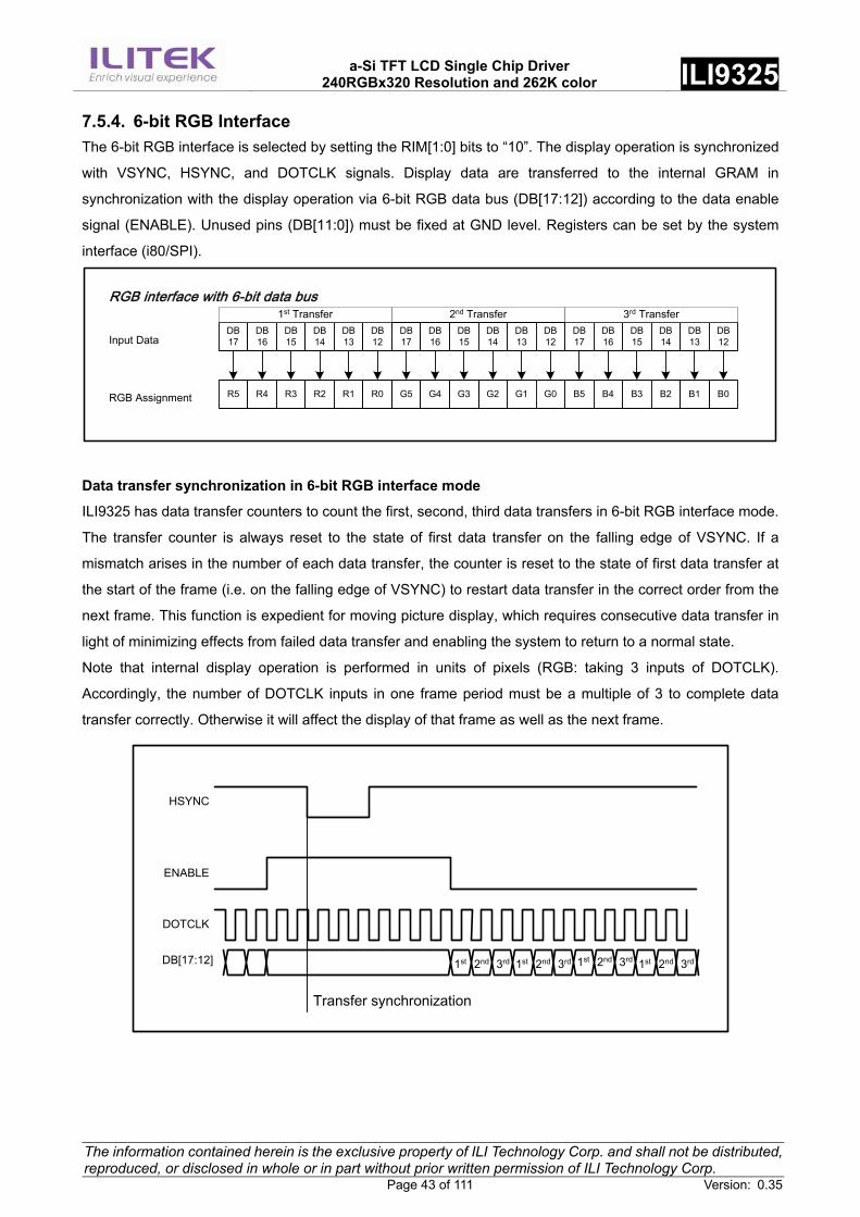
a-Si TFT LCD Single Chip Driver
240RGBx320 Resolution and 262K color ILI9325
The information contained herein is the exclusive property of ILI Technology Corp. and shall not be distributed, reproduced, or disclosed in whole or in part without prior written permission of ILI Technology Corp. Page 43 of 111 Version: 0.35
7.5.4. 6-bit RGB Interface The 6-bit RGB interface is selected by setting the RIM[1:0] bits to “10”. The display operation is synchronized
with VSYNC, HSYNC, and DOTCLK signals. Display data are transferred to the internal GRAM in
synchronization with the display operation via 6-bit RGB data bus (DB[17:12]) according to the data enable
signal (ENABLE). Unused pins (DB[11:0]) must be fixed at GND level. Registers can be set by the system
interface (i80/SPI).
Input Data
RGB Assignment
RGB interface with 6-bit data bus
DB17
DB16
DB15
DB14
DB13
DB12
R5 R4 R3 R2 R1 R0 G5 G4 G2 G1 G0 B5 B4 B3 B2 B1G3 B0
1st Transfer 2nd TransferDB17
DB16
DB15
DB14
DB13
DB12
DB17
DB16
DB15
DB14
DB13
DB12
3rd Transfer
Data transfer synchronization in 6-bit RGB interface mode
ILI9325 has data transfer counters to count the first, second, third data transfers in 6-bit RGB interface mode.
The transfer counter is always reset to the state of first data transfer on the falling edge of VSYNC. If a
mismatch arises in the number of each data transfer, the counter is reset to the state of first data transfer at
the start of the frame (i.e. on the falling edge of VSYNC) to restart data transfer in the correct order from the
next frame. This function is expedient for moving picture display, which requires consecutive data transfer in
light of minimizing effects from failed data transfer and enabling the system to return to a normal state.
Note that internal display operation is performed in units of pixels (RGB: taking 3 inputs of DOTCLK).
Accordingly, the number of DOTCLK inputs in one frame period must be a multiple of 3 to complete data
transfer correctly. Otherwise it will affect the display of that frame as well as the next frame.
HSYNC
ENABLE
DOTCLK
DB[17:12] 1st 2nd 3rd 1st 2nd 3rd 1st 2nd 3rd 1st 2nd 3rd
Transfer synchronization
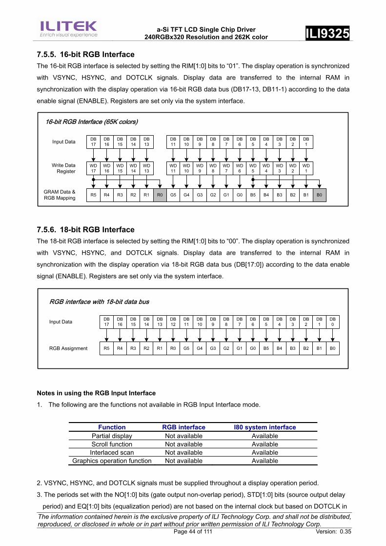
a-Si TFT LCD Single Chip Driver
240RGBx320 Resolution and 262K color ILI9325
The information contained herein is the exclusive property of ILI Technology Corp. and shall not be distributed, reproduced, or disclosed in whole or in part without prior written permission of ILI Technology Corp. Page 44 of 111 Version: 0.35
7.5.5. 16-bit RGB Interface The 16-bit RGB interface is selected by setting the RIM[1:0] bits to “01”. The display operation is synchronized
with VSYNC, HSYNC, and DOTCLK signals. Display data are transferred to the internal RAM in
synchronization with the display operation via 16-bit RGB data bus (DB17-13, DB11-1) according to the data
enable signal (ENABLE). Registers are set only via the system interface.
16-bit RGB Interface (65K colors)
Input Data
Write Data Register
R5 R4 R3 R2 R1 R0 G5 G4 G2 G1 G0 B5 B4 B3 B2 B1G3GRAM Data & RGB Mapping B0
WD17
WD16
WD15
WD14
WD13
WD11
WD10
WD9
WD8
WD7
WD6
WD5
WD4
WD3
WD2
WD1
DB17
DB16
DB15
DB14
DB13
DB11
DB10
DB9
DB8
DB7
DB6
DB5
DB4
DB3
DB2
DB1
7.5.6. 18-bit RGB Interface The 18-bit RGB interface is selected by setting the RIM[1:0] bits to “00”. The display operation is synchronized
with VSYNC, HSYNC, and DOTCLK signals. Display data are transferred to the internal RAM in
synchronization with the display operation via 18-bit RGB data bus (DB[17:0]) according to the data enable
signal (ENABLE). Registers are set only via the system interface.
DB17
DB16
DB15
DB14
DB13
DB12
DB11
DB10
DB9
DB8
DB7
DB6
DB5
DB4
DB3
DB2
DB1
DB0
RGB Assignment R5 R4 R3 R2 R1 R0 G5 G4 G2 G1 G0 B5 B4 B3 B2 B1G3 B0
RGB interface with 18-bit data bus
Input Data
Notes in using the RGB Input Interface
1. The following are the functions not available in RGB Input Interface mode.
Function RGB interface I80 system interface Partial display Not available Available Scroll function Not available Available Interlaced scan Not available Available
Graphics operation function Not available Available
2. VSYNC, HSYNC, and DOTCLK signals must be supplied throughout a display operation period.
3. The periods set with the NO[1:0] bits (gate output non-overlap period), STD[1:0] bits (source output delay
period) and EQ[1:0] bits (equalization period) are not based on the internal clock but based on DOTCLK in
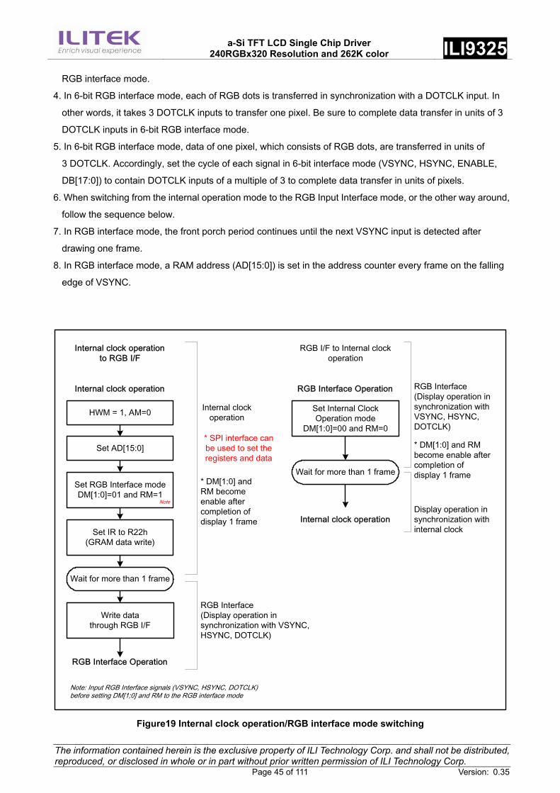
a-Si TFT LCD Single Chip Driver
240RGBx320 Resolution and 262K color ILI9325
The information contained herein is the exclusive property of ILI Technology Corp. and shall not be distributed, reproduced, or disclosed in whole or in part without prior written permission of ILI Technology Corp. Page 45 of 111 Version: 0.35
RGB interface mode.
4. In 6-bit RGB interface mode, each of RGB dots is transferred in synchronization with a DOTCLK input. In
other words, it takes 3 DOTCLK inputs to transfer one pixel. Be sure to complete data transfer in units of 3
DOTCLK inputs in 6-bit RGB interface mode.
5. In 6-bit RGB interface mode, data of one pixel, which consists of RGB dots, are transferred in units of
3 DOTCLK. Accordingly, set the cycle of each signal in 6-bit interface mode (VSYNC, HSYNC, ENABLE,
DB[17:0]) to contain DOTCLK inputs of a multiple of 3 to complete data transfer in units of pixels.
6. When switching from the internal operation mode to the RGB Input Interface mode, or the other way around,
follow the sequence below.
7. In RGB interface mode, the front porch period continues until the next VSYNC input is detected after
drawing one frame.
8. In RGB interface mode, a RAM address (AD[15:0]) is set in the address counter every frame on the falling
edge of VSYNC.
HWM = 1, AM=0
Set AD[15:0]
Set RGB Interface modeDM[1:0]=01 and RM=1
Set IR to R22h(GRAM data write)
Wait for more than 1 frame
Write datathrough RGB I/F
Internal clock operationto RGB I/F
Internal clockoperation
* DM[1:0] andRM becomeenable aftercompletion ofdisplay 1 frame
RGB Interface Operation
RGB Interface(Display operation insynchronization with VSYNC,HSYNC, DOTCLK)
* SPI interface canbe used to set theregisters and data
RGB I/F to Internal clockoperation
* DM[1:0] and RMbecome enable aftercompletion ofdisplay 1 frame
Internal clock operation RGB Interface Operation
Set Internal ClockOperation mode
DM[1:0]=00 and RM=0
Wait for more than 1 frame
Internal clock operation
RGB Interface(Display operation insynchronization withVSYNC, HSYNC,DOTCLK)
Display operation insynchronization withinternal clock
Note
Note: Input RGB Interface signals (VSYNC, HSYNC, DOTCLK)before setting DM[1;0] and RM to the RGB interface mode
Figure19 Internal clock operation/RGB interface mode switching
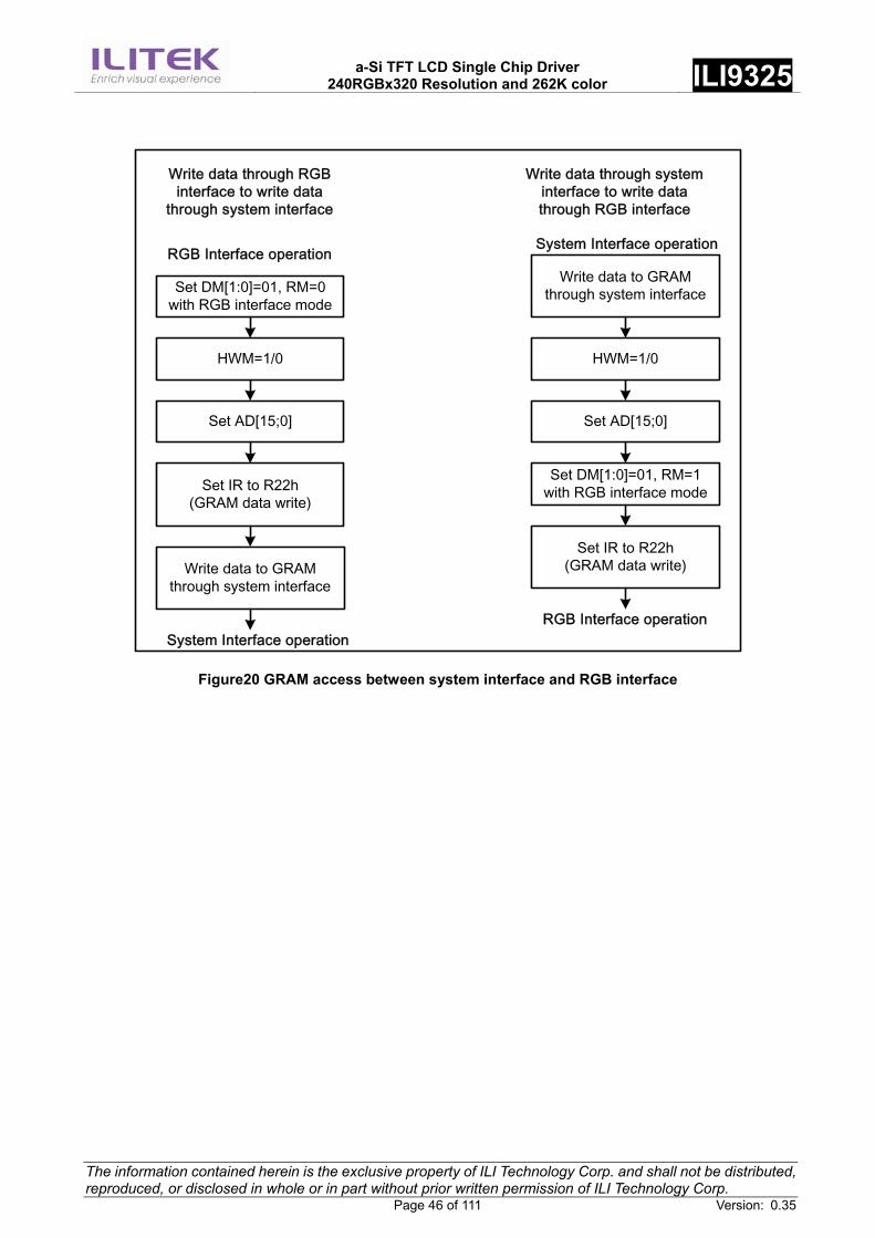
a-Si TFT LCD Single Chip Driver
240RGBx320 Resolution and 262K color ILI9325
The information contained herein is the exclusive property of ILI Technology Corp. and shall not be distributed, reproduced, or disclosed in whole or in part without prior written permission of ILI Technology Corp. Page 46 of 111 Version: 0.35
Set DM[1:0]=01, RM=0with RGB interface mode
HWM=1/0
Set AD[15;0]
Set IR to R22h(GRAM data write)
Write data through RGBinterface to write data
through system interface
RGB Interface operation
Write data to GRAMthrough system interface
Write data through systeminterface to write datathrough RGB interface
Write data to GRAMthrough system interface
HWM=1/0
Set AD[15;0]
Set DM[1:0]=01, RM=1with RGB interface mode
Set IR to R22h(GRAM data write)
RGB Interface operationSystem Interface operation
System Interface operation
Figure20 GRAM access between system interface and RGB interface
a-Si TFT LCD Single Chip Driver
240RGBx320 Resolution and 262K color ILI9325
The information contained herein is the exclusive property of ILI Technology Corp. and shall not be distributed, reproduced, or disclosed in whole or in part without prior written permission of ILI Technology Corp. Page 47 of 111 Version: 0.35
7.6. Interface Timing The following are diagrams of interfacing timing with LCD panel control signals in internal operation and RGB
interface modes.
1 2 3 4 5 320319318 1 2
//
//
//
//
//
G1
FLM
G2
G320
…..
1 2 3 4 5 320319318//
S[720:1]
VCOM
DB[17:0]
ENABLE
DOTCLK
HSYNC
VSYNC
3 4
Figure21 Relationship between RGB I/F signals and LCD Driving Signals for Panel
a-Si TFT LCD Single Chip Driver
240RGBx320 Resolution and 262K color ILI9325
The information contained herein is the exclusive property of ILI Technology Corp. and shall not be distributed, reproduced, or disclosed in whole or in part without prior written permission of ILI Technology Corp. Page 48 of 111 Version: 0.35
8. Register Descriptions
8.1. Registers Access ILI9325 adopts 18-bit bus interface architecture for high-performance microprocessor. All the functional
blocks of ILI9325 starts to work after receiving the correct instruction from the external microprocessor by the
18-, 16-, 9-, 8-bit interface. The index register (IR) stores the register address to which the instructions and
display data will be written. The register selection signal (RS), the read/write signals (nRD/nWR) and data
bus D17-0 are used to read/write the instructions and data of ILI9325. The registers of the ILI9325 are
categorized into the following groups.
1. Specify the index of register (IR)
2. Read a status
3. Display control
4. Power management Control
5. Graphics data processing
6. Set internal GRAM address (AC)
7. Transfer data to/from the internal GRAM (R22)
8. Internal grayscale γ-correction (R30 ~ R39)
Normally, the display data (GRAM) is most often updated, and in order since the ILI9325 can update internal
GRAM address automatically as it writes data to the internal GRAM and minimize data transfer by using the
window address function, there are fewer loads on the program in the microprocessor. As the following figure
shows, the way of assigning data to the 16 register bits (D[15:0]) varies for each interface. Send registers in
accordance with the following data transfer format.
Serial Peripheral Interface for register access
SPI Input Data D15
D14
D13
D12
D11
D10
D8
D7
D6
D5
D4
D3
D2
D1
Register Data D15
D14
D13
D12
D11
D10
D8
D7
D6
D5
D4
D3
D2
D1
D9
D9
D0
D0
Figure22 Register Setting with Serial Peripheral Interface (SPI)
a-Si TFT LCD Single Chip Driver
240RGBx320 Resolution and 262K color ILI9325
The information contained herein is the exclusive property of ILI Technology Corp. and shall not be distributed, reproduced, or disclosed in whole or in part without prior written permission of ILI Technology Corp. Page 49 of 111 Version: 0.35
DB17
DB16
DB15
DB14
DB13
DB12
DB11
DB10
DB9
DB8
DB7
DB6
DB5
DB4
DB3
DB2
DB1
DB0
i80/M68 system 18-bit data bus interface
Data Bus(DB[17:0])
Register Bit(D[15:0]) D15 D14 D13 D12 D11 D10 D9 D8 D7 D6 D5 D4 D3 D2 D1 D0
DB17
DB16
DB15
DB14
DB13
DB12
DB11
DB10
DB8
DB7
DB6
DB5
DB4
DB3
DB2
DB1
i80/M68 system 16-bit data bus interface
Data Bus(DB[17:10]),(DB[8:1])
Register Bit(D[15:0]) D15 D14 D13 D12 D11 D10 D9 D8 D7 D6 D5 D4 D3 D2 D1 D0
DB17
DB16
DB15
DB14
DB13
DB12
DB11
DB10
DB9
i80/M68 system 9-bit data bus interface
Data Bus(DB[17:9])
Register Bit(D[15:0]) D15 D14 D13 D12 D11 D10 D9 D8 D7 D6 D5 D4 D3 D2 D1 D0
1st TransferDB17
DB16
DB15
DB14
DB13
DB12
DB11
DB10
DB9
2nd Transfer
DB17
DB16
DB15
DB14
DB13
DB12
DB11
DB10
i80/M68 system 8-bit data bus interface/Serial peripheral interface (2/3 transmission)
Data Bus(DB[17:10])
Register Bit(D[15:0]) D15 D14 D13 D12 D11 D10 D9 D8 D7 D6 D5 D4 D3 D2 D1 D0
1st TransferDB17
DB16
DB15
DB14
DB13
DB12
DB11
DB10
2nd Transfer
Figure23 Register setting with i80 System Interface
a-Si TFT LCD Single Chip Driver
240RGBx320 Resolution and 262K color ILI9325
The information contained herein is the exclusive property of ILI Technology Corp. and shall not be distributed, reproduced, or disclosed in whole or in part without prior written permission of ILI Technology Corp. Page 50 of 111 Version: 0.35
i80 18-/16-bit System Bus Interface Timing
Write register “index” Write register “data”
nWR
DB[17:0]
nRD
RS
nCS
(a) Write to register
Write register “index” Read register “data”
nWR
DB[17:0]
nRD
RS
nCS
(b) Read from register
i80 9-/8-bit System Bus Interface Timing
“00h” Write register “index”
nWR
DB[17:10]
nRD
RS
nCS
(a) Write to register
(b) Read from register
Write register“high byte data”
Write register“low byte data”
“00h” Write register “index”
nWR
DB[17:10]
nRD
RS
nCS
Read register“high byte data”
Read register“low byte data”
Figure 24 Register Read/Write Timing of i80 System Interface
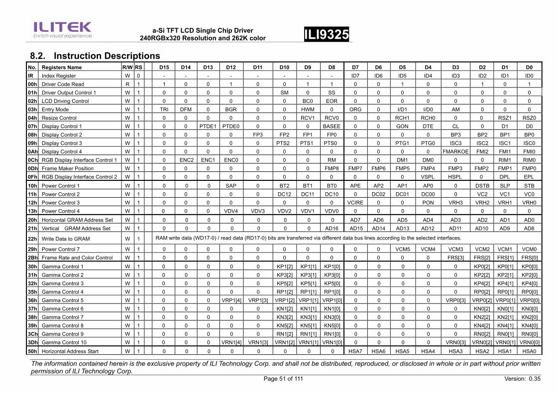
a-Si TFT LCD Single Chip Driver
240RGBx320 Resolution and 262K color ILI9325
The information contained herein is the exclusive property of ILI Technology Corp. and shall not be distributed, reproduced, or disclosed in whole or in part without prior written permission of ILI Technology Corp. Page 51 of 111 Version: 0.35
8.2. Instruction Descriptions No. Registers Name R/W RS D15 D14 D13 D12 D11 D10 D9 D8 D7 D6 D5 D4 D3 D2 D1 D0 IR Index Register W 0 - - - - - - - - ID7 ID6 ID5 ID4 ID3 ID2 ID1 ID0 00h Driver Code Read R 1 1 0 0 1 0 0 1 1 0 0 1 0 0 1 0 1 01h Driver Output Control 1 W 1 0 0 0 0 0 SM 0 SS 0 0 0 0 0 0 0 0 02h LCD Driving Control W 1 0 0 0 0 0 0 BC0 EOR 0 0 0 0 0 0 0 0 03h Entry Mode W 1 TRI DFM 0 BGR 0 0 HWM 0 ORG 0 I/D1 I/D0 AM 0 0 0 04h Resize Control W 1 0 0 0 0 0 0 RCV1 RCV0 0 0 RCH1 RCH0 0 0 RSZ1 RSZ0 07h Display Control 1 W 1 0 0 PTDE1 PTDE0 0 0 0 BASEE 0 0 GON DTE CL 0 D1 D0 08h Display Control 2 W 1 0 0 0 0 FP3 FP2 FP1 FP0 0 0 0 0 BP3 BP2 BP1 BP0 09h Display Control 3 W 1 0 0 0 0 0 PTS2 PTS1 PTS0 0 0 PTG1 PTG0 ISC3 ISC2 ISC1 ISC0 0Ah Display Control 4 W 1 0 0 0 0 0 0 0 0 0 0 0 0 FMARKOE FMI2 FMI1 FMI0 0Ch RGB Display Interface Control 1 W 1 0 ENC2 ENC1 ENC0 0 0 0 RM 0 0 DM1 DM0 0 0 RIM1 RIM0 0Dh Frame Maker Position W 1 0 0 0 0 0 0 0 FMP8 FMP7 FMP6 FMP5 FMP4 FMP3 FMP2 FMP1 FMP0 0Fh RGB Display Interface Control 2 W 1 0 0 0 0 0 0 0 0 0 0 0 VSPL HSPL 0 DPL EPL
10h Power Control 1 W 1 0 0 0 SAP 0 BT2 BT1 BT0 APE AP2 AP1 AP0 0 DSTB SLP STB 11h Power Control 2 W 1 0 0 0 0 0 DC12 DC11 DC10 0 DC02 DC01 DC00 0 VC2 VC1 VC0 12h Power Control 3 W 1 0 0 0 0 0 0 0 0 VCIRE 0 0 PON VRH3 VRH2 VRH1 VRH0 13h Power Control 4 W 1 0 0 0 VDV4 VDV3 VDV2 VDV1 VDV0 0 0 0 0 0 0 0 0
20h Horizontal GRAM Address Set W 1 0 0 0 0 0 0 0 0 AD7 AD6 AD5 AD4 AD3 AD2 AD1 AD0 21h Vertical GRAM Address Set W 1 0 0 0 0 0 0 0 AD16 AD15 AD14 AD13 AD12 AD11 AD10 AD9 AD8
22h Write Data to GRAM W 1 RAM write data (WD17-0) / read data (RD17-0) bits are transferred via different data bus lines according to the selected interfaces.
29h Power Control 7 W 1 0 0 0 0 0 0 0 0 0 0 VCM5 VCM4 VCM3 VCM2 VCM1 VCM0 2Bh Frame Rate and Color Control W 1 0 0 0 0 0 0 0 0 0 0 0 0 FRS[3] FRS[2] FRS[1] FRS[0]
30h Gamma Control 1 W 1 0 0 0 0 0 KP1[2] KP1[1] KP1[0] 0 0 0 0 0 KP0[2] KP0[1] KP0[0] 31h Gamma Control 2 W 1 0 0 0 0 0 KP3[2] KP3[1] KP3[0] 0 0 0 0 0 KP2[2] KP2[1] KP2[0] 32h Gamma Control 3 W 1 0 0 0 0 0 KP5[2] KP5[1] KP5[0] 0 0 0 0 0 KP4[2] KP4[1] KP4[0] 35h Gamma Control 4 W 1 0 0 0 0 0 RP1[2] RP1[1] RP1[0] 0 0 0 0 0 RP0[2] RP0[1] RP0[0] 36h Gamma Control 5 W 1 0 0 0 VRP1[4] VRP1[3] VRP1[2] VRP1[1] VRP1[0] 0 0 0 0 VRP0[3] VRP0[2] VRP0[1] VRP0[0] 37h Gamma Control 6 W 1 0 0 0 0 0 KN1[2] KN1[1] KN1[0] 0 0 0 0 0 KN0[2] KN0[1] KN0[0] 38h Gamma Control 7 W 1 0 0 0 0 0 KN3[2] KN3[1] KN3[0] 0 0 0 0 0 KN2[2] KN2[1] KN2[0] 39h Gamma Control 8 W 1 0 0 0 0 0 KN5[2] KN5[1] KN5[0] 0 0 0 0 0 KN4[2] KN4[1] KN4[0] 3Ch Gamma Control 9 W 1 0 0 0 0 0 RN1[2] RN1[1] RN1[0] 0 0 0 0 0 RN0[2] RN0[1] RN0[0] 3Dh Gamma Control 10 W 1 0 0 0 VRN1[4] VRN1[3] VRN1[2] VRN1[1] VRN1[0] 0 0 0 0 VRN0[3] VRN0[2] VRN0[1] VRN0[0]
50h Horizontal Address Start W 1 0 0 0 0 0 0 0 0 HSA7 HSA6 HSA5 HSA4 HSA3 HSA2 HSA1 HSA0
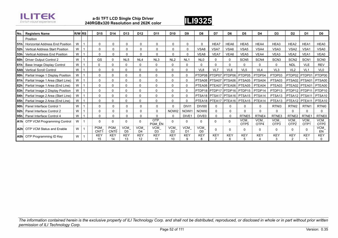
a-Si TFT LCD Single Chip Driver
240RGBx320 Resolution and 262K color ILI9325
The information contained herein is the exclusive property of ILI Technology Corp. and shall not be distributed, reproduced, or disclosed in whole or in part without prior written permission of ILI Technology Corp. Page 52 of 111 Version: 0.35
No. Registers Name R/W RS D15 D14 D13 D12 D11 D10 D9 D8 D7 D6 D5 D4 D3 D2 D1 D0 Position
51h Horizontal Address End Position W 1 0 0 0 0 0 0 0 0 HEA7 HEA6 HEA5 HEA4 HEA3 HEA2 HEA1 HEA0 52h Vertical Address Start Position W 1 0 0 0 0 0 0 0 VSA8 VSA7 VSA6 VSA5 VSA4 VSA3 VSA2 VSA1 VSA0 53h Vertical Address End Position W 1 0 0 0 0 0 0 0 VEA8 VEA7 VEA6 VEA5 VEA4 VEA3 VEA2 VEA1 VEA0
60h Driver Output Control 2 W 1 GS 0 NL5 NL4 NL3 NL2 NL1 NL0 0 0 SCN5 SCN4 SCN3 SCN2 SCN1 SCN0 61h Base Image Display Control W 1 0 0 0 0 0 0 0 0 0 0 0 0 0 NDL VLE REV 6Ah Vertical Scroll Control W 1 0 0 0 0 0 0 0 VL8 VL7 VL6 VL5 VL4 VL3 VL2 VL1 VL0
80h Partial Image 1 Display Position W 1 0 0 0 0 0 0 0 PTDP08 PTDP07 PTDP06 PTDP05 PTDP04 PTDP03 PTDP02 PTDP01 PTDP00 81h Partial Image 1 Area (Start Line) W 1 0 0 0 0 0 0 0 PTSA08 PTSA07 PTSA06 PTSA05 PTSA04 PTSA03 PTSA02 PTSA01 PTSA00 82h Partial Image 1 Area (End Line) W 1 0 0 0 0 0 0 0 PTEA08 PTEA07 PTEA06 PTEA05 PTEA04 PTEA03 PTEA02 PTEA01 PTEA00 83h Partial Image 2 Display Position W 1 0 0 0 0 0 0 0 PTDP18 PTDP17 PTDP16 PTDP15 PTDP14 PTDP13 PTDP12 PTDP11 PTDP10 84h Partial Image 2 Area (Start Line) W 1 0 0 0 0 0 0 0 PTSA18 PTSA17 PTSA16 PTSA15 PTSA14 PTSA13 PTSA12 PTSA11 PTSA10 85h Partial Image 2 Area (End Line) W 1 0 0 0 0 0 0 0 PTEA18 PTEA17 PTEA16 PTEA15 PTEA14 PTEA13 PTEA12 PTEA11 PTEA10
90h Panel Interface Control 1 W 1 0 0 0 0 0 0 DIVI1 DIVI00 0 0 0 0 RTNI3 RTNI2 RTNI1 RTNI0 92h Panel Interface Control 2 W 1 0 0 0 0 0 NOWI2 NOWI1 NOWI0 0 0 0 0 0 0 0 0 95h Panel Interface Control 4 W 1 0 0 0 0 0 0 DIVE1 DIVE0 0 0 RTNE5 RTNE4 RTNE3 RTNE2 RTNE1 RTNE0
A1h OTP VCM Programming Control W 1 0 0 0 0 OTP_ PGM_EN
0 0 0 0 0 VCM_OTP5
VCM_OTP4
VCM_ OTP3
VCM_ OTP2
VCM_ OTP1
VCM_ OTP0
A2h OTP VCM Status and Enable W 1 PGM_CNT1
PGM_CNT0
VCM_D5
VCM_D4
VCM_ D3
VCM_D2
VCM_ D1
VCM_D0 0 0 0 0 0 0 0 VCM_
EN A5h OTP Programming ID Key W 1 KEY
15 KEY14
KEY13
KEY 12
KEY 11
KEY 10
KEY 9
KEY 8
KEY 7
KEY 6
KEY 5
KEY 4
KEY 3
KEY 2
KEY 1
KEY 0
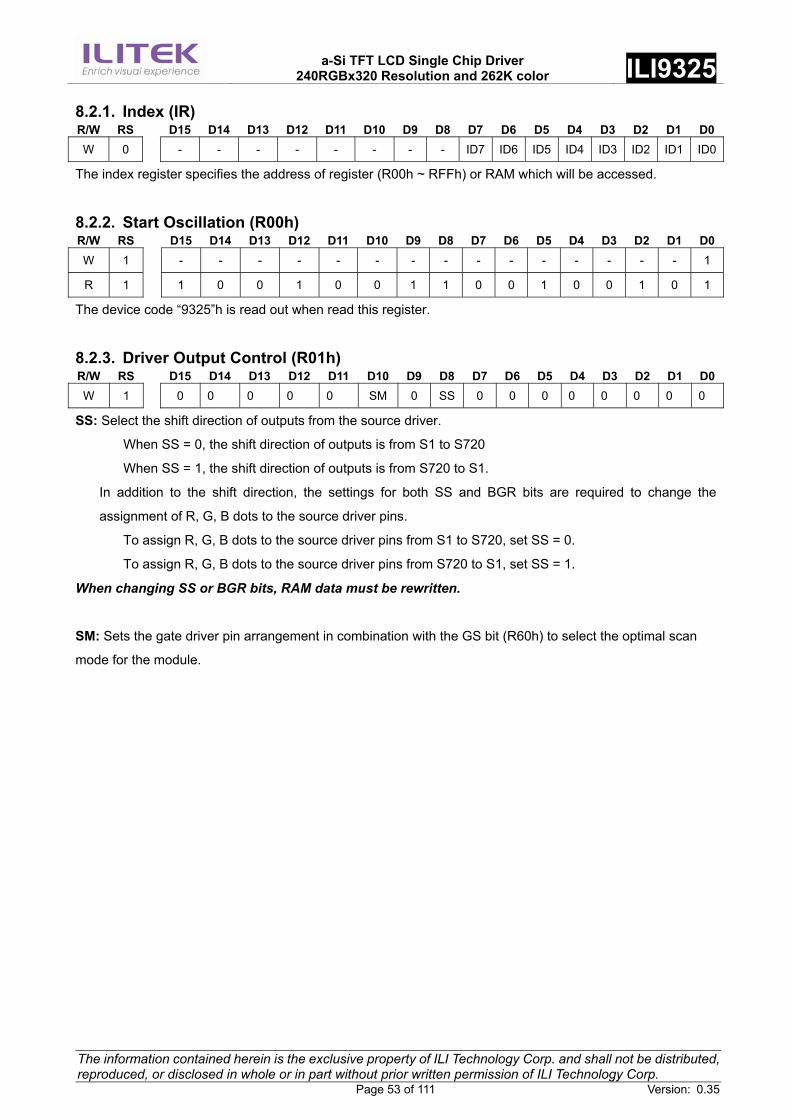
a-Si TFT LCD Single Chip Driver
240RGBx320 Resolution and 262K color ILI9325
The information contained herein is the exclusive property of ILI Technology Corp. and shall not be distributed, reproduced, or disclosed in whole or in part without prior written permission of ILI Technology Corp. Page 53 of 111 Version: 0.35
8.2.1. Index (IR) R/W RS D15 D14 D13 D12 D11 D10 D9 D8 D7 D6 D5 D4 D3 D2 D1 D0W 0 - - - - - - - - ID7 ID6 ID5 ID4 ID3 ID2 ID1 ID0
The index register specifies the address of register (R00h ~ RFFh) or RAM which will be accessed.
8.2.2. Start Oscillation (R00h) R/W RS D15 D14 D13 D12 D11 D10 D9 D8 D7 D6 D5 D4 D3 D2 D1 D0W 1 - - - - - - - - - - - - - - - 1
R 1 1 0 0 1 0 0 1 1 0 0 1 0 0 1 0 1
The device code “9325”h is read out when read this register.
8.2.3. Driver Output Control (R01h) R/W RS D15 D14 D13 D12 D11 D10 D9 D8 D7 D6 D5 D4 D3 D2 D1 D0W 1 0 0 0 0 0 SM 0 SS 0 0 0 0 0 0 0 0
SS: Select the shift direction of outputs from the source driver.
When SS = 0, the shift direction of outputs is from S1 to S720
When SS = 1, the shift direction of outputs is from S720 to S1.
In addition to the shift direction, the settings for both SS and BGR bits are required to change the
assignment of R, G, B dots to the source driver pins.
To assign R, G, B dots to the source driver pins from S1 to S720, set SS = 0.
To assign R, G, B dots to the source driver pins from S720 to S1, set SS = 1.
When changing SS or BGR bits, RAM data must be rewritten.
SM: Sets the gate driver pin arrangement in combination with the GS bit (R60h) to select the optimal scan
mode for the module.
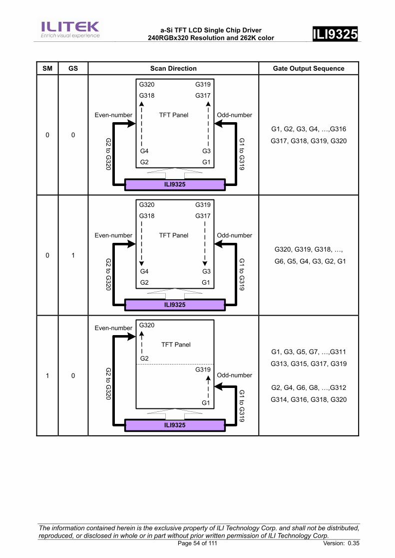
a-Si TFT LCD Single Chip Driver
240RGBx320 Resolution and 262K color ILI9325
The information contained herein is the exclusive property of ILI Technology Corp. and shall not be distributed, reproduced, or disclosed in whole or in part without prior written permission of ILI Technology Corp. Page 54 of 111 Version: 0.35
SM GS Scan Direction Gate Output Sequence
0 0
G1
G3
G317
G319
G2
G4
G318
G320
ILI9325
Odd-numberEven-number
G1 to G
319
TFT Panel
G2 to G
320
G1, G2, G3, G4, …,G316
G317, G318, G319, G320
0 1 G2 to G
320 G1
G3
G317
G319
ILI9325
Odd-numberEven-number TFT Panel
G1 to G
319G2
G4
G318
G320
G320, G319, G318, …,
G6, G5, G4, G3, G2, G1
1 0
G1
G319
G320
ILI9325
Odd-number
Even-number
G2
TFT Panel
G1 to G
319
G2 to G
320
G1, G3, G5, G7, …,G311
G313, G315, G317, G319
G2, G4, G6, G8, …,G312
G314, G316, G318, G320
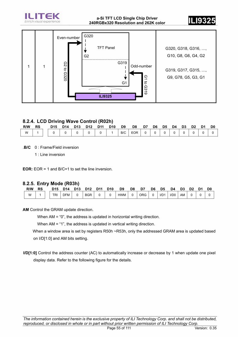
a-Si TFT LCD Single Chip Driver
240RGBx320 Resolution and 262K color ILI9325
The information contained herein is the exclusive property of ILI Technology Corp. and shall not be distributed, reproduced, or disclosed in whole or in part without prior written permission of ILI Technology Corp. Page 55 of 111 Version: 0.35
1 1
G320
G2
G1
ILI9325
Odd-number
Even-number
G319
TFT Panel
G2 to G
320
G1 to G
319
G320, G318, G316, …,
G10, G8, G6, G4, G2
G319, G317, G315, …,
G9, G78, G5, G3, G1
8.2.4. LCD Driving Wave Control (R02h) R/W RS D15 D14 D13 D12 D11 D10 D9 D8 D7 D6 D5 D4 D3 D2 D1 D0
W 1 0 0 0 0 0 1 B/C EOR 0 0 0 0 0 0 0 0
.B/C 0 : Frame/Field inversion
1 : Line inversion
EOR: EOR = 1 and B/C=1 to set the line inversion.
8.2.5. Entry Mode (R03h) R/W RS D15 D14 D13 D12 D11 D10 D9 D8 D7 D6 D5 D4 D3 D2 D1 D0
W 1 TRI DFM 0 BGR 0 0 HWM 0 ORG 0 I/D1 I/D0 AM 0 0 0
AM Control the GRAM update direction.
When AM = “0”, the address is updated in horizontal writing direction.
When AM = “1”, the address is updated in vertical writing direction.
When a window area is set by registers R50h ~R53h, only the addressed GRAM area is updated based
on I/D[1:0] and AM bits setting.
I/D[1:0] Control the address counter (AC) to automatically increase or decrease by 1 when update one pixel
display data. Refer to the following figure for the details.
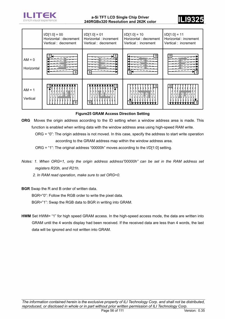
a-Si TFT LCD Single Chip Driver
240RGBx320 Resolution and 262K color ILI9325
The information contained herein is the exclusive property of ILI Technology Corp. and shall not be distributed, reproduced, or disclosed in whole or in part without prior written permission of ILI Technology Corp. Page 56 of 111 Version: 0.35
I/D[1:0] = 00Horizontal : decrementVertical : decrement
I/D[1:0] = 01Horizontal : incrementVertical : decrement
I/D[1:0] = 10Horizontal : decrementVertical : increment
I/D[1:0] = 11Horizontal : incrementVertical : increment
AM = 0
Horizontal
AM = 1
Vertical
B
E
B
E B
E
B
E
B
E
B
EB
E
B
E
Figure25 GRAM Access Direction Setting
ORG Moves the origin address according to the ID setting when a window address area is made. This
function is enabled when writing data with the window address area using high-speed RAM write.
ORG = “0”: The origin address is not moved. In this case, specify the address to start write operation
according to the GRAM address map within the window address area.
ORG = “1”: The original address “00000h” moves according to the I/D[1:0] setting.
Notes: 1. When ORG=1, only the origin address address”00000h” can be set in the RAM address set
registers R20h, and R21h.
2. In RAM read operation, make sure to set ORG=0.
BGR Swap the R and B order of written data.
BGR=”0”: Follow the RGB order to write the pixel data.
BGR=”1”: Swap the RGB data to BGR in writing into GRAM.
HWM Set HWM= “1” for high speed GRAM access. In the high-speed access mode, the data are written into
GRAM until the 4 words display had been received. If the received data are less than 4 words, the last
data will be ignored and not written into GRAM.
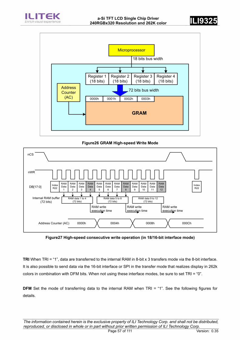
a-Si TFT LCD Single Chip Driver
240RGBx320 Resolution and 262K color ILI9325
The information contained herein is the exclusive property of ILI Technology Corp. and shall not be distributed, reproduced, or disclosed in whole or in part without prior written permission of ILI Technology Corp. Page 57 of 111 Version: 0.35
Microprocessor
Register 1(18 bits)
Register 2(18 bits)
Register 3(18 bits)
Register 4(18 bits)
0000h 0001h 0002h 0003h
GRAM
72 bits bus width
18 bits bus width
AddressCounter
(AC)
Figure26 GRAM High-speed Write Mode
IndexR22
RAMData
1
RAMData
2
RAMData
3
RAMData
4
RAMData
5
RAMData
6
RAMData
7
RAMData
8
RAMData
9
RAMData10
RAMData11
RAMData12
RAM writeexecution time
RAM data 5 to 8(72 bits)
RAM writeexecution time
RAM writeexecution time
Address Counter (AC) 0000h 0004h 0008h 000Ch
IndexR22
Internal RAM buffer(72 bits)
nCS
nWR
DB[17:0]
RAM data 1 to 4(72 bits)
RAM data 9 to 12(72 bits)
Figure27 High-speed consecutive write operation (in 18/16-bit interface mode)
TRI When TRI = “1”, data are transferred to the internal RAM in 8-bit x 3 transfers mode via the 8-bit interface.
It is also possible to send data via the 16-bit interface or SPI in the transfer mode that realizes display in 262k
colors in combination with DFM bits. When not using these interface modes, be sure to set TRI = “0”.
DFM Set the mode of transferring data to the internal RAM when TRI = “1”. See the following figures for
details.
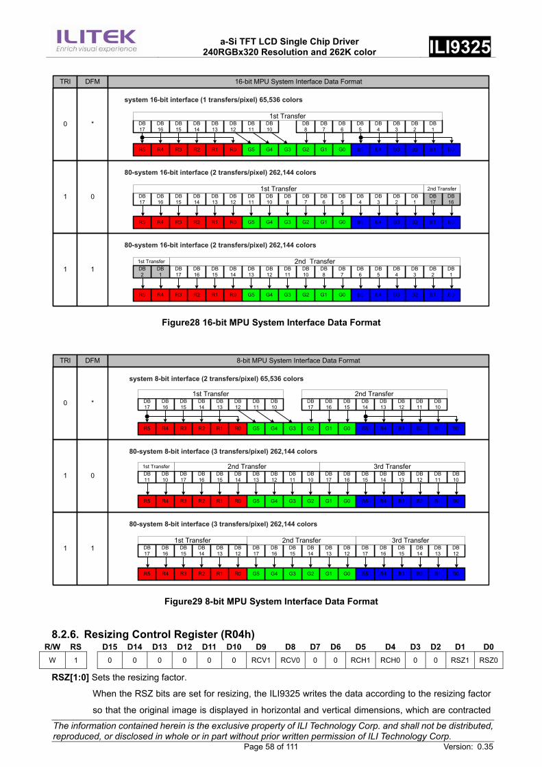
a-Si TFT LCD Single Chip Driver
240RGBx320 Resolution and 262K color ILI9325
The information contained herein is the exclusive property of ILI Technology Corp. and shall not be distributed, reproduced, or disclosed in whole or in part without prior written permission of ILI Technology Corp. Page 58 of 111 Version: 0.35
TRI DFM 16-bit MPU System Interface Data Format
R4R5 R2R3 R0R1 G4G5 G2G3 G0G1 B4B5 B2B3 B0B1
0 *
system 16-bit interface (1 transfers/pixel) 65,536 colors
R4R5 R2R3 R0R1 G4G5 G2G3 G0G1 B4B5 B2B3 B0B1
1 0
80-system 16-bit interface (2 transfers/pixel) 262,144 colors
R4R5 R2R3 R0R1 G4G5 G2G3 G0G1 B4B5 B2B3 B0B1
1 1
80-system 16-bit interface (2 transfers/pixel) 262,144 colors
DB16
DB17
DB14
DB15
DB12
DB13
DB10
DB11
DB7
DB8
DB5
DB6
DB3
DB4
DB1
DB2
1st Transfer
DB16
DB17
DB14
DB15
DB12
DB13
DB10
DB11
DB7
DB8
DB5
DB6
DB3
DB4
DB1
DB2
1st TransferDB16
DB17
2nd Transfer
DB16
DB17
DB14
DB15
DB12
DB13
DB10
DB11
DB7
DB8
DB5
DB6
DB3
DB4
DB1
DB2
2nd Transfer1st TransferDB1
DB2
Figure28 16-bit MPU System Interface Data Format
TRI DFM 8-bit MPU System Interface Data Format
DB16
DB17
DB14
DB15
DB12
DB13
DB10
DB11
DB16
DB17
DB14
DB15
DB12
DB13
DB10
DB11
R4R5 R2R3 R0R1 G4G5 G2G3 G0G1 B4B5 B2B3 B0B1
1st Transfer 2nd Transfer0 *
system 8-bit interface (2 transfers/pixel) 65,536 colors
DB16
DB17
DB14
DB15
DB12
DB13
DB10
DB11
DB16
DB17
DB14
DB15
DB12
DB13
DB10
DB11
R4R5 R2R3 R0R1 G4G5 G2G3 G0G1 B4B5 B2B3 B0B1
2nd Transfer 3rd Transfer1 0
80-system 8-bit interface (3 transfers/pixel) 262,144 colors
DB10
DB11
1st Transfer
R4R5 R2R3 R0R1 G4G5 G2G3 G0G1 B4B5 B2B3 B0B1
1 1
80-system 8-bit interface (3 transfers/pixel) 262,144 colors
DB16
DB17
DB14
DB15
DB12
DB13
DB16
DB17
DB14
DB15
DB12
DB13
2nd Transfer 3rd Transfer1st TransferDB16
DB17
DB14
DB15
DB12
DB13
Figure29 8-bit MPU System Interface Data Format
8.2.6. Resizing Control Register (R04h) R/W RS D15 D14 D13 D12 D11 D10 D9 D8 D7 D6 D5 D4 D3 D2 D1 D0
W 1 0 0 0 0 0 0 RCV1 RCV0 0 0 RCH1 RCH0 0 0 RSZ1 RSZ0
RSZ[1:0] Sets the resizing factor.
When the RSZ bits are set for resizing, the ILI9325 writes the data according to the resizing factor
so that the original image is displayed in horizontal and vertical dimensions, which are contracted
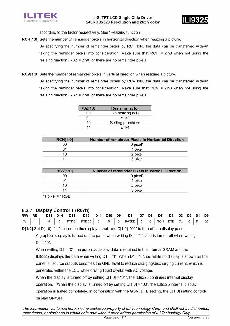
a-Si TFT LCD Single Chip Driver
240RGBx320 Resolution and 262K color ILI9325
The information contained herein is the exclusive property of ILI Technology Corp. and shall not be distributed, reproduced, or disclosed in whole or in part without prior written permission of ILI Technology Corp. Page 59 of 111 Version: 0.35
according to the factor respectively. See “Resizing function”.
RCH[1:0] Sets the number of remainder pixels in horizontal direction when resizing a picture.
By specifying the number of remainder pixels by RCH bits, the data can be transferred without
taking the reminder pixels into consideration. Make sure that RCH = 2’h0 when not using the
resizing function (RSZ = 2’h0) or there are no remainder pixels.
RCV[1:0] Sets the number of remainder pixels in vertical direction when resizing a picture.
By specifying the number of remainder pixels by RCV bits, the data can be transferred without
taking the reminder pixels into consideration. Make sure that RCV = 2’h0 when not using the
resizing function (RSZ = 2’h0) or there are no remainder pixels.
RSZ[1:0] Resizing factor
00 No resizing (x1) 01 x 1/2 10 Setting prohibited 11 x 1/4
RCH[1:0] Number of remainder Pixels in Horizontal Direction
00 0 pixel* 01 1 pixel 10 2 pixel 11 3 pixel
RCV[1:0] Number of remainder Pixels in Vertical Direction
00 0 pixel* 01 1 pixel 10 2 pixel 11 3 pixel
*1 pixel = 1RGB
8.2.7. Display Control 1 (R07h) R/W RS D15 D14 D13 D12 D11 D10 D9 D8 D7 D6 D5 D4 D3 D2 D1 D0
W 1 0 0 PTDE1 PTDE0 0 0 0 BASEE 0 0 GON DTE CL 0 D1 D0
D[1:0] Set D[1:0]=”11” to turn on the display panel, and D[1:0]=”00” to turn off the display panel.
A graphics display is turned on the panel when writing D1 = “1”, and is turned off when writing
D1 = “0”.
When writing D1 = “0”, the graphics display data is retained in the internal GRAM and the
ILI9325 displays the data when writing D1 = “1”. When D1 = “0”, i.e. while no display is shown on the
panel, all source outputs becomes the GND level to reduce charging/discharging current, which is
generated within the LCD while driving liquid crystal with AC voltage.
When the display is turned off by setting D[1:0] = “01”, the ILI9325 continues internal display
operation. When the display is turned off by setting D[1:0] = “00”, the ILI9325 internal display
operation is halted completely. In combination with the GON, DTE setting, the D[1:0] setting controls
display ON/OFF.
a-Si TFT LCD Single Chip Driver
240RGBx320 Resolution and 262K color ILI9325
The information contained herein is the exclusive property of ILI Technology Corp. and shall not be distributed, reproduced, or disclosed in whole or in part without prior written permission of ILI Technology Corp. Page 60 of 111 Version: 0.35
D1 D0 BASEE Source, VCOM Output ILI9325 internal operation 0 0 0 GND Halt 0 1 1 GND Operate 1 0 0 Non-lit display Operate 1 1 0 Non-lit display Operate 1 1 1 Base image display Operate
Note: 1. data write operation from the microcontroller is performed irrespective of the setting of D[1:0] bits.
2. The D[1:0] setting is valid on both 1st and 2nd displays.
3. The non-lit display level from the source output pins is determined by instruction (PTS).
CL When CL = “1”, the 8-color display mode is selected.
CL Colors 0 262,144 1 8
GON and DTE Set the output level of gate driver G1 ~ G320 as follows
GON DTE G1 ~G320 Gate Output 0 0 VGH 0 1 VGH 1 0 VGL 1 1 Normal Display
BASEE
Base image display enable bit. When BASEE = “0”, no base image is displayed. The ILI9325 drives
liquid crystal at non-lit display level or displays only partial images. When BASEE = “1”, the base
image is displayed. The D[1:0] setting has higher priority over the BASEE setting.
PTDE[1:0]
Partial image 2 and Partial image 1 enable bits
PTDE1/0 = 0: turns off partial image. Only base image is displayed.
PTDE1/0 = 1: turns on partial image. Set the base image display enable bit to 0 (BASEE = 0).
8.2.8. Display Control 2 (R08h) R/W RS D15 D14 D13 D12 D11 D10 D9 D8 D7 D6 D5 D4 D3 D2 D1 D0
W 1 0 0 0 0 FP3 FP2 FP1 FP0 0 0 0 0 BP3 BP2 BP1 BP0
FP[3:0]/BP[3:0]
The FP[3:0] and BP[3:0] bits specify the line number of front and back porch periods respectively.
When setting the FP[3:0] and BP[3:0] value, the following conditions shall be met:
BP + FP ≤ 16 lines
FP ≥ 2 lines
BP ≥ 2 lines
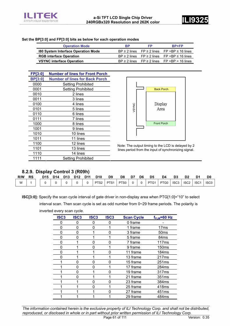
a-Si TFT LCD Single Chip Driver
240RGBx320 Resolution and 262K color ILI9325
The information contained herein is the exclusive property of ILI Technology Corp. and shall not be distributed, reproduced, or disclosed in whole or in part without prior written permission of ILI Technology Corp. Page 61 of 111 Version: 0.35
Set the BP[3:0] and FP[3:0] bits as below for each operation modes Operation Mode BP FP BP+FP
I80 System Interface Operation Mode BP ≥ 2 lines FP ≥ 2 lines FP +BP ≤ 16 linesRGB interface Operation BP ≥ 2 lines FP ≥ 2 lines FP +BP ≤ 16 linesVSYNC interface Operation BP ≥ 2 lines FP ≥ 2 lines FP +BP = 16 lines
FP[3:0] Number of lines for Front Porch BP[3:0] Number of lines for Back Porch
0000 Setting Prohibited 0001 Setting Prohibited 0010 2 lines 0011 3 lines 0100 4 lines 0101 5 lines 0110 6 lines 0111 7 lines 1000 8 lines 1001 9 lines 1010 10 lines 1011 11 lines 1100 12 lines 1101 13 lines 1110 14 lines 1111 Setting Prohibited
DisplayArea
Back Porch
Front Porch
VSY
NC
Note: The output timing to the LCD is delayed by 2lines period from the input of synchronizing signal.
8.2.9. Display Control 3 (R09h) R/W RS D15 D14 D13 D12 D11 D10 D9 D8 D7 D6 D5 D4 D3 D2 D1 D0
W 1 0 0 0 0 0 PTS2 PTS1 PTS0 0 0 PTG1 PTG0 ISC3 ISC2 ISC1 ISC0
ISC[3:0]: Specify the scan cycle interval of gate driver in non-display area when PTG[1:0]=”10” to select
interval scan. Then scan cycle is set as odd number from 0~29 frame periods. The polarity is
inverted every scan cycle.
ISC3 ISC3 ISC3 ISC3 Scan Cycle fFLM=60 Hz 0 0 0 0 0 frame - 0 0 0 1 1 frame 17ms 0 0 1 0 3 frame 50ms 0 0 1 1 5 frame 84ms 0 1 0 0 7 frame 117ms 0 1 0 1 9 frame 150ms 0 1 1 0 11 frame 184ms 0 1 1 1 13 frame 217ms 1 0 0 0 15 frame 251ms 1 0 0 1 17 frame 284ms 1 0 1 0 19 frame 317ms 1 0 1 1 21 frame 351ms 1 1 0 0 23 frame 384ms 1 1 0 1 25 frame 418ms 1 1 1 0 27 frame 451ms 1 1 1 1 29 frame 484ms
a-Si TFT LCD Single Chip Driver
240RGBx320 Resolution and 262K color ILI9325
The information contained herein is the exclusive property of ILI Technology Corp. and shall not be distributed, reproduced, or disclosed in whole or in part without prior written permission of ILI Technology Corp. Page 62 of 111 Version: 0.35
PTG[1:0] Set the scan mode in non-display area.
PTG1 PTG0 Gate outputs in non-display area Source outputs in non-display area Vcom output 0 0 Normal scan Set with the PTS[2:0] bits VcomH/VcomL0 1 Setting Prohibited - - 1 0 Interval scan Set with the PTS[2:0] bits VcomH/VcomL1 1 Setting Prohibited - -
PTS[2:0]
Set the source output level in non-display area drive period (front/back porch period and blank area
between partial displays).
When PTS[2] = 1, the operation of amplifiers which generates the grayscales other than V0 and V63
are halted and the step-up clock frequency becomes half the normal frequency in non-display drive
period in order to reduce power consumption.
Source output level
PTS[2:0] Positive polarity Negative polarity
Grayscale amplifierin operation
Step-up clock frequency
000 V63 V0 V63 to V0 Register Setting (DC1, DC0) 001 Setting Prohibited Setting Prohibited - - 010 GND GND V63 to V0 Register Setting (DC1, DC0) 011 Hi-Z Hi-Z V63 to V0 Register Setting (DC1, DC0) 100 V63 V0 V63 and V0 frequency setting by DC1, DC0101 Setting Prohibited Setting Prohibited - - 110 GND GND V63 and V0 frequency setting by DC1, DC0111 Hi-Z Hi-Z V63 and V0 frequency setting by DC1, DC0
Notes: 1. The power efficiency can be improved by halting grayscale amplifiers and slowing down the step-up clock frequency only in non-display drive period.
2. The gate output level in non-lit display area drive period is determined by PTG[1:0].
8.2.10. Display Control 4 (R0Ah) R/W RS D15 D14 D13 D12 D11 D10 D9 D8 D7 D6 D5 D4 D3 D2 D1 D0
W 1 0 0 0 0 0 0 0 0 0 0 0 0 FMARKOE FMI2 FMI1 FMI0
FMI[2:0] Set the output interval of FMARK signal according to the display data rewrite cycle and data transfer
rate.
FMARKOE When FMARKOE=1, ILI9325 starts to output FMARK signal in the output interval set by FMI[2:0]
bits. FMI[2:0] Output Interval
000 1 frame 001 2 frame 011 4 frame 101 6 frame
Others Setting disabled
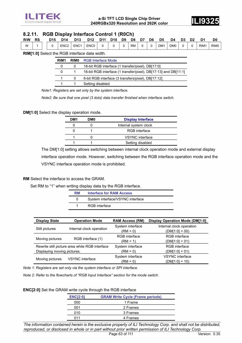
a-Si TFT LCD Single Chip Driver
240RGBx320 Resolution and 262K color ILI9325
The information contained herein is the exclusive property of ILI Technology Corp. and shall not be distributed, reproduced, or disclosed in whole or in part without prior written permission of ILI Technology Corp. Page 63 of 111 Version: 0.35
8.2.11. RGB Display Interface Control 1 (R0Ch) R/W RS D15 D14 D13 D12 D11 D10 D9 D8 D7 D6 D5 D4 D3 D2 D1 D0
W 1 0 ENC2 ENC1 ENC0 0 0 0 RM 0 0 DM1 DM0 0 0 RIM1 RIM0
RIM[1:0] Select the RGB interface data width.
RIM1 RIM0 RGB Interface Mode 0 0 18-bit RGB interface (1 transfer/pixel), DB[17:0] 0 1 16-bit RGB interface (1 transfer/pixel), DB[17:13] and DB[11:1]
1 0 6-bit RGB interface (3 transfers/pixel), DB[17:12] 1 1 Setting disabled
Note1: Registers are set only by the system interface.
Note2: Be sure that one pixel (3 dots) data transfer finished when interface switch.
DM[1:0] Select the display operation mode.
DM1 DM0 Display Interface 0 0 Internal system clock 0 1 RGB interface
1 0 VSYNC interface 1 1 Setting disabled
The DM[1:0] setting allows switching between internal clock operation mode and external display
interface operation mode. However, switching between the RGB interface operation mode and the
VSYNC interface operation mode is prohibited.
RM Select the interface to access the GRAM.
Set RM to “1” when writing display data by the RGB interface.
RM Interface for RAM Access 0 System interface/VSYNC interface
1 RGB interface
Display State Operation Mode RAM Access (RM) Display Operation Mode (DM[1:0]
Still pictures Internal clock operationSystem interface
(RM = 0) Internal clock operation
(DM[1:0] = 00)
Moving pictures RGB interface (1) RGB interface
(RM = 1) RGB interface (DM[1:0] = 01)
Rewrite still picture area while RGB interface Displaying moving pictures.
System interface (RM = 0)
RGB interface (DM[1:0] = 01)
Moving pictures VSYNC interface System interface
(RM = 0) VSYNC interface
(DM[1:0] = 10)
Note 1: Registers are set only via the system interface or SPI interface.
Note 2: Refer to the flowcharts of “RGB Input Interface” section for the mode switch.
ENC[2:0] Set the GRAM write cycle through the RGB interface
ENC[2:0] GRAM Write Cycle (Frame periods) 000 1 Frame 001 2 Frames 010 3 Frames 011 4 Frames
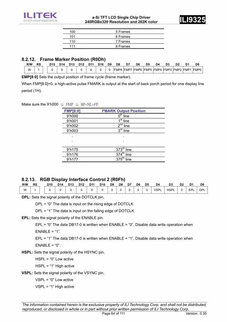
a-Si TFT LCD Single Chip Driver
240RGBx320 Resolution and 262K color ILI9325
The information contained herein is the exclusive property of ILI Technology Corp. and shall not be distributed, reproduced, or disclosed in whole or in part without prior written permission of ILI Technology Corp. Page 64 of 111 Version: 0.35
100 5 Frames 101 6 Frames 110 7 Frames 111 8 Frames
8.2.12. Frame Marker Position (R0Dh) R/W RS D15 D14 D13 D12 D11 D10 D9 D8 D7 D6 D5 D4 D3 D2 D1 D0
W 1 0 0 0 0 0 0 0 FMP8 FMP7 FMP6 FMP5 FMP4 FMP3 FMP2 FMP1 FMP0
EMP[8:0] Sets the output position of frame cycle (frame marker).
When FMP[8:0]=0, a high-active pulse FMARK is output at the start of back porch period for one display line
period (1H).
Make sure the 9’h000 ≦ FMP ≦ BP+NL+FP
FMP[8:0] FMARK Output Position 9’h000 0th line 9’h001 1st line 9’h002 2nd line 9’h003 3rd line
.
.
.
.
.
. 9’h175 373rd line 9’h176 374th line 9’h177 375th line
8.2.13. RGB Display Interface Control 2 (R0Fh) R/W RS D15 D14 D13 D12 D11 D10 D9 D8 D7 D6 D5 D4 D3 D2 D1 D0
W 1 0 0 0 0 0 0 0 0 0 0 0 VSPL HSPL 0 EPL DPL
DPL: Sets the signal polarity of the DOTCLK pin.
DPL = “0” The data is input on the rising edge of DOTCLK
DPL = “1” The data is input on the falling edge of DOTCLK
EPL: Sets the signal polarity of the ENABLE pin.
EPL = “0” The data DB17-0 is written when ENABLE = “0”. Disable data write operation when
ENABLE = “1”.
EPL = “1” The data DB17-0 is written when ENABLE = “1”. Disable data write operation when
ENABLE = “0”.
HSPL: Sets the signal polarity of the HSYNC pin.
HSPL = “0” Low active
HSPL = “1” High active
VSPL: Sets the signal polarity of the VSYNC pin.
VSPL = “0” Low active
VSPL = “1” High active
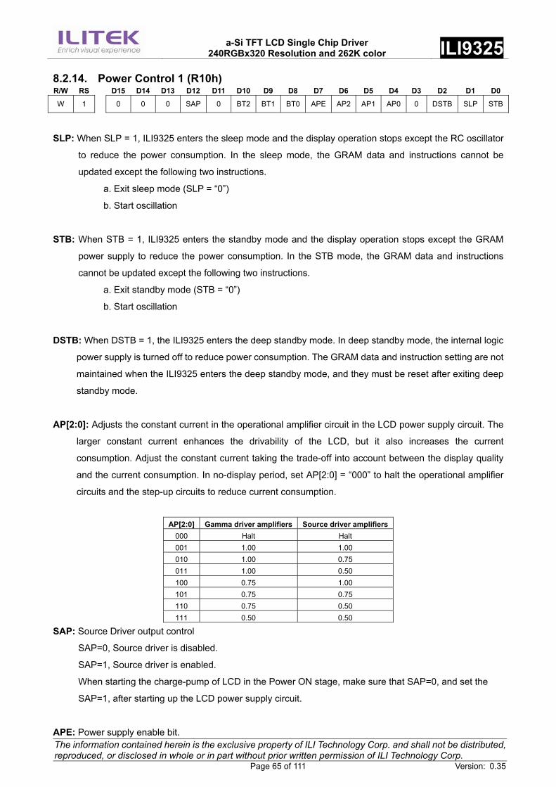
a-Si TFT LCD Single Chip Driver
240RGBx320 Resolution and 262K color ILI9325
The information contained herein is the exclusive property of ILI Technology Corp. and shall not be distributed, reproduced, or disclosed in whole or in part without prior written permission of ILI Technology Corp. Page 65 of 111 Version: 0.35
8.2.14. Power Control 1 (R10h) R/W RS D15 D14 D13 D12 D11 D10 D9 D8 D7 D6 D5 D4 D3 D2 D1 D0
W 1 0 0 0 SAP 0 BT2 BT1 BT0 APE AP2 AP1 AP0 0 DSTB SLP STB
SLP: When SLP = 1, ILI9325 enters the sleep mode and the display operation stops except the RC oscillator
to reduce the power consumption. In the sleep mode, the GRAM data and instructions cannot be
updated except the following two instructions.
a. Exit sleep mode (SLP = “0”)
b. Start oscillation
STB: When STB = 1, ILI9325 enters the standby mode and the display operation stops except the GRAM
power supply to reduce the power consumption. In the STB mode, the GRAM data and instructions
cannot be updated except the following two instructions.
a. Exit standby mode (STB = “0”)
b. Start oscillation
DSTB: When DSTB = 1, the ILI9325 enters the deep standby mode. In deep standby mode, the internal logic
power supply is turned off to reduce power consumption. The GRAM data and instruction setting are not
maintained when the ILI9325 enters the deep standby mode, and they must be reset after exiting deep
standby mode.
AP[2:0]: Adjusts the constant current in the operational amplifier circuit in the LCD power supply circuit. The
larger constant current enhances the drivability of the LCD, but it also increases the current
consumption. Adjust the constant current taking the trade-off into account between the display quality
and the current consumption. In no-display period, set AP[2:0] = “000” to halt the operational amplifier
circuits and the step-up circuits to reduce current consumption.
AP[2:0] Gamma driver amplifiers Source driver amplifiers
000 Halt Halt 001 1.00 1.00 010 1.00 0.75 011 1.00 0.50 100 0.75 1.00 101 0.75 0.75 110 0.75 0.50 111 0.50 0.50
SAP: Source Driver output control
SAP=0, Source driver is disabled.
SAP=1, Source driver is enabled.
When starting the charge-pump of LCD in the Power ON stage, make sure that SAP=0, and set the
SAP=1, after starting up the LCD power supply circuit.
APE: Power supply enable bit.
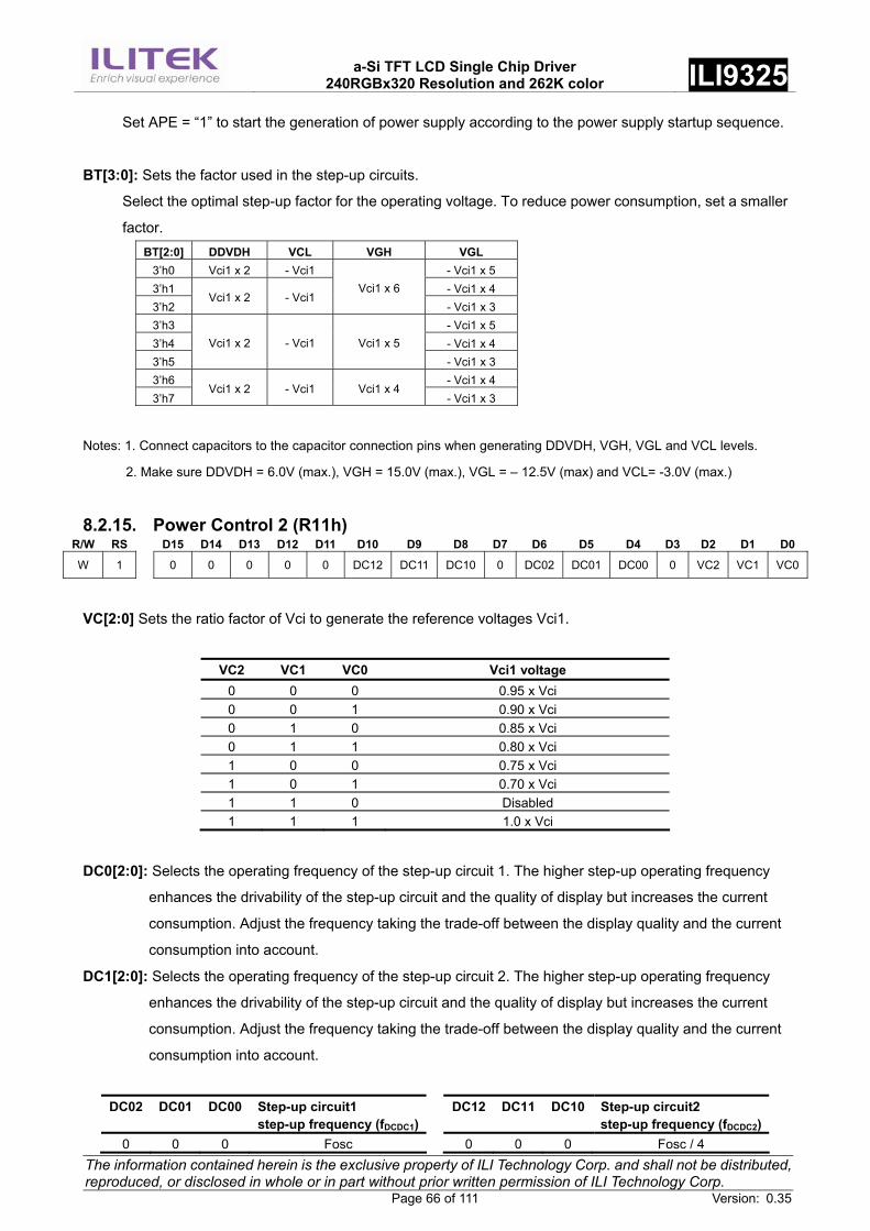
a-Si TFT LCD Single Chip Driver
240RGBx320 Resolution and 262K color ILI9325
The information contained herein is the exclusive property of ILI Technology Corp. and shall not be distributed, reproduced, or disclosed in whole or in part without prior written permission of ILI Technology Corp. Page 66 of 111 Version: 0.35
Set APE = “1” to start the generation of power supply according to the power supply startup sequence.
BT[3:0]: Sets the factor used in the step-up circuits.
Select the optimal step-up factor for the operating voltage. To reduce power consumption, set a smaller
factor. BT[2:0] DDVDH VCL VGH VGL
3’h0 Vci1 x 2 - Vci1 - Vci1 x 5 3’h1 - Vci1 x 4 3’h2
Vci1 x 2 - Vci1 Vci1 x 6
- Vci1 x 3 3’h3 - Vci1 x 5 3’h4 - Vci1 x 4 3’h5
Vci1 x 2 - Vci1 Vci1 x 5 - Vci1 x 3
3’h6 - Vci1 x 4 3’h7
Vci1 x 2 - Vci1 Vci1 x 4 - Vci1 x 3
Notes: 1. Connect capacitors to the capacitor connection pins when generating DDVDH, VGH, VGL and VCL levels.
2. Make sure DDVDH = 6.0V (max.), VGH = 15.0V (max.), VGL = – 12.5V (max) and VCL= -3.0V (max.)
8.2.15. Power Control 2 (R11h) R/W RS D15 D14 D13 D12 D11 D10 D9 D8 D7 D6 D5 D4 D3 D2 D1 D0
W 1 0 0 0 0 0 DC12 DC11 DC10 0 DC02 DC01 DC00 0 VC2 VC1 VC0
VC[2:0] Sets the ratio factor of Vci to generate the reference voltages Vci1.
VC2 VC1 VC0 Vci1 voltage 0 0 0 0.95 x Vci 0 0 1 0.90 x Vci 0 1 0 0.85 x Vci 0 1 1 0.80 x Vci 1 0 0 0.75 x Vci 1 0 1 0.70 x Vci 1 1 0 Disabled 1 1 1 1.0 x Vci
DC0[2:0]: Selects the operating frequency of the step-up circuit 1. The higher step-up operating frequency
enhances the drivability of the step-up circuit and the quality of display but increases the current
consumption. Adjust the frequency taking the trade-off between the display quality and the current
consumption into account.
DC1[2:0]: Selects the operating frequency of the step-up circuit 2. The higher step-up operating frequency
enhances the drivability of the step-up circuit and the quality of display but increases the current
consumption. Adjust the frequency taking the trade-off between the display quality and the current
consumption into account.
DC02 DC01 DC00 Step-up circuit1 step-up frequency (fDCDC1)
DC12 DC11 DC10 Step-up circuit2 step-up frequency (fDCDC2)
0 0 0 Fosc 0 0 0 Fosc / 4
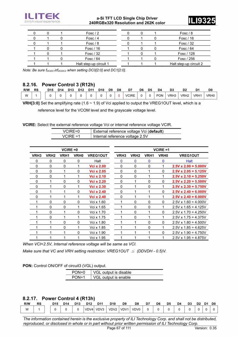
a-Si TFT LCD Single Chip Driver
240RGBx320 Resolution and 262K color ILI9325
The information contained herein is the exclusive property of ILI Technology Corp. and shall not be distributed, reproduced, or disclosed in whole or in part without prior written permission of ILI Technology Corp. Page 67 of 111 Version: 0.35
0 0 1 Fosc / 2 0 0 1 Fosc / 8 0 1 0 Fosc / 4 0 1 0 Fosc / 16 0 1 1 Fosc / 8 0 1 1 Fosc / 32 1 0 0 Fosc / 16 1 0 0 Fosc / 64 1 0 1 Fosc / 32 1 0 1 Fosc / 128 1 1 0 Fosc / 64 1 1 0 Fosc / 256 1 1 1 Halt step-up circuit 1 1 1 1 Halt step-up circuit 2
Note: Be sure fDCDC1≥fDCDC2 when setting DC0[2:0] and DC1[2:0].
8.2.16. Power Control 3 (R12h) R/W RS D15 D14 D13 D12 D11 D10 D9 D8 D7 D6 D5 D4 D3 D2 D1 D0
W 1 0 0 0 0 0 0 0 0 VCIRE 0 0 PON VRH3 VRH2 VRH1 VRH0
VRH[3:0] Set the amplifying rate (1.6 ~ 1.9) of Vci applied to output the VREG1OUT level, which is a
reference level for the VCOM level and the grayscale voltage level.
VCIRE: Select the external reference voltage Vci or internal reference voltage VCIR. VCIRE=0 External reference voltage Vci (default) VCIRE =1 Internal reference voltage 2.5V
VCIRE =0 VCIRE =1 VRH3 VRH2 VRH1 VRH0 VREG1OUT VRH3 VRH2 VRH1 VRH0 VREG1OUT
0 0 0 0 Halt 0 0 0 0 Halt 0 0 0 1 Vci x 2.00 0 0 0 1 2.5V x 2.00 = 5.000V0 0 1 0 Vci x 2.05 0 0 1 0 2.5V x 2.05 = 5.125V0 0 1 1 Vci x 2.10 0 0 1 1 2.5V x 2.10 = 5.250V0 1 0 0 Vci x 2.20 0 1 0 0 2.5V x 2.20 = 5.500V0 1 0 1 Vci x 2.30 0 1 0 1 2.5V x 2.30 = 5.750V0 1 1 0 Vci x 2.40 0 1 1 0 2.5V x 2.40 = 6.000V0 1 1 1 Vci x 2.40 0 1 1 1 2.5V x 2.40 = 6.000V1 0 0 0 Vci x 1.60 1 0 0 0 2.5V x 1.60 = 4.000V1 0 0 1 Vci x 1.65 1 0 0 1 2.5V x 1.65 = 4.125V1 0 1 0 Vci x 1.70 1 0 1 0 2.5V x 1.70 = 4.250V1 0 1 1 Vci x 1.75 1 0 1 1 2.5V x 1.75 = 4.375V1 1 0 0 Vci x 1.80 1 1 0 0 2.5V x 1.80 = 4.500V1 1 0 1 Vci x 1.85 1 1 0 1 2.5V x 1.85 = 4.625V1 1 1 0 Vci x 1.90 1 1 1 0 2.5V x 1.90 = 4.750V1 1 1 1 Vci x 1.95 1 1 1 1 2.5V x 1.95 = 4.875V
When VCI<2.5V, Internal reference voltage will be same as VCI.
Make sure that VC and VRH setting restriction: VREG1OUT ≦ (DDVDH - 0.5)V.
PON: Control ON/OFF of circuit3 (VGL) output. PON=0 VGL output is disable PON=1 VGL output is enable
8.2.17. Power Control 4 (R13h) R/W RS D15 D14 D13 D12 D11 D10 D9 D8 D7 D6 D5 D4 D3 D2 D1 D0
W 1 0 0 0 VDV4 VDV3 VDV2 VDV1 VDV0 0 0 0 0 0 0 0 0
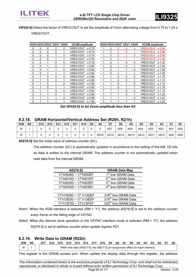
a-Si TFT LCD Single Chip Driver
240RGBx320 Resolution and 262K color ILI9325
The information contained herein is the exclusive property of ILI Technology Corp. and shall not be distributed, reproduced, or disclosed in whole or in part without prior written permission of ILI Technology Corp. Page 68 of 111 Version: 0.35
VDV[4:0] Select the factor of VREG1OUT to set the amplitude of Vcom alternating voltage from 0.70 to 1.24 x
VREG1OUT .
VDV4 VDV3 VDV2 VDV1 VDV0 VCOM amplitude VDV4 VDV3 VDV2 VDV1 VDV0 VCOM amplitude
0 0 0 0 0 VREG1OUT x 0.70 1 0 0 0 0 VREG1OUT x 0.940 0 0 0 1 VREG1OUT x 0.72 1 0 0 0 1 VREG1OUT x 0.960 0 0 1 0 VREG1OUT x 0.74 1 0 0 1 0 VREG1OUT x 0.980 0 0 1 1 VREG1OUT x 0.76 1 0 0 1 1 VREG1OUT x 1.000 0 1 0 0 VREG1OUT x 0.78 1 0 1 0 0 VREG1OUT x 1.020 0 1 0 1 VREG1OUT x 0.80 1 0 1 0 1 VREG1OUT x 1.040 0 1 1 0 VREG1OUT x 0.82 1 0 1 1 0 VREG1OUT x 1.060 0 1 1 1 VREG1OUT x 0.84 1 0 1 1 1 VREG1OUT x 1.080 1 0 0 0 VREG1OUT x 0.86 1 1 0 0 0 VREG1OUT x 1.100 1 0 0 1 VREG1OUT x 0.88 1 1 0 0 1 VREG1OUT x 1.120 1 0 1 0 VREG1OUT x 0.90 1 1 0 1 0 VREG1OUT x 1.140 1 0 1 1 VREG1OUT x 0.92 1 1 0 1 1 VREG1OUT x 1.160 1 1 0 0 VREG1OUT x 0.94 1 1 1 0 0 VREG1OUT x 1.180 1 1 0 1 VREG1OUT x 0.96 1 1 1 0 1 VREG1OUT x 1.200 1 1 1 0 VREG1OUT x 0.98 1 1 1 1 0 VREG1OUT x 1.220 1 1 1 1 VREG1OUT x 1.00 1 1 1 1 1 VREG1OUT x 1.24
Set VDV[4:0] to let Vcom amplitude less than 6V. 8.2.18. GRAM Horizontal/Vertical Address Set (R20h, R21h) R/W RS D15 D14 D13 D12 D11 D10 D9 D8 D7 D6 D5 D4 D3 D2 D1 D0
W 1 0 0 0 0 0 0 0 0 AD7 AD6 AD5 AD4 AD3 AD2 AD1 AD0
W 1 0 0 0 0 0 0 0 AD16 AD15 AD14 AD13 AD12 AD11 AD10 AD9 AD8
AD[16:0] Set the initial value of address counter (AC).
The address counter (AC) is automatically updated in accordance to the setting of the AM, I/D bits
as data is written to the internal GRAM. The address counter is not automatically updated when
read data from the internal GRAM.
AD[16:0] GRAM Data Map 17’h00000 ~ 17’h000EF 1st line GRAM Data 17’h00100 ~ 17’h001EF 2nd line GRAM Data 17’h00200 ~ 17’h002EF 3rd line GRAM Data 17’h00300 ~ 17’h003EF 4th line GRAM Data
17’h13D00 ~ 17’ h13DEF 318th line GRAM Data 17’h13E00 ~ 17’ h13EEF 319th line GRAM Data 17’h13F00 ~ 17’h13FEF 320th line GRAM Data
Note1: When the RGB interface is selected (RM = “1”), the address AD[16:0] is set to the address counter
every frame on the falling edge of VSYNC.
Note2: When the internal clock operation or the VSYNC interface mode is selected (RM = “0”), the address
AD[16:0] is set to address counter when update register R21.
8.2.19. Write Data to GRAM (R22h) R/W RS D17 D16 D15 D14 D13 D12 D11 D10 D9 D8 D7 D6 D5 D4 D3 D2 D1 D0
W 1 RAM write data (WD[17:0], the DB[17:0] pin assignment differs for each interface.
This register is the GRAM access port. When update the display data through this register, the address
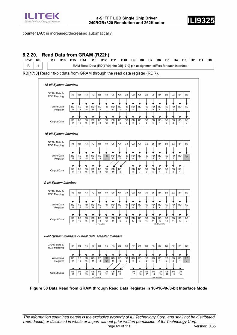
a-Si TFT LCD Single Chip Driver
240RGBx320 Resolution and 262K color ILI9325
The information contained herein is the exclusive property of ILI Technology Corp. and shall not be distributed, reproduced, or disclosed in whole or in part without prior written permission of ILI Technology Corp. Page 69 of 111 Version: 0.35
counter (AC) is increased/decreased automatically.
8.2.20. Read Data from GRAM (R22h) R/W RS D17 D16 D15 D14 D13 D12 D11 D10 D9 D8 D7 D6 D5 D4 D3 D2 D1 D0
R 1 RAM Read Data (RD[17:0], the DB[17:0] pin assignment differs for each interface.
RD[17:0] Read 18-bit data from GRAM through the read data register (RDR).
DB17
DB16
DB15
DB14
DB13
DB12
DB11
DB10
DB9
DB8
DB7
DB6
DB5
DB4
DB3
DB2
DB1
DB0
18-bit System Interface
Output Data
Write DataRegister
R5 R4 R3 R2 R1 R0 G5 G4 G2 G1 G0 B5 B4 B3 B2 B1G3GRAM Data &RGB Mapping B0
RD17
RD16
RD15
RD14
RD13
RD12
RD11
RD10
RD9
RD8
RD7
RD6
RD5
RD4
RD3
RD2
RD1
RD0
DB17
DB16
DB15
DB14
DB13
DB12
DB11
DB10
DB8
DB7
DB6
DB5
DB4
DB3
DB2
DB1
16-bit System Interface
Output Data
Write DataRegister
R5 R4 R3 R2 R1 R0 G5 G4 G2 G1 G0 B5 B4 B3 B2 B1G3GRAM Data &RGB Mapping B0
RD17
RD16
RD15
RD14
RD13
RD12
RD11
RD10
RD9
RD8
RD7
RD6
RD5
RD4
RD3
RD2
RD1
RD0
DB17
DB16
DB15
DB14
DB13
DB12
DB11
DB10
DB9
9-bit System Interface
Output Data
Write DataRegister
R5 R4 R3 R2 R1 R0 G5 G4 G2 G1 G0 B5 B4 B3 B2 B1G3GRAM Data &RGB Mapping B0
RD17
RD16
RD15
RD14
RD13
RD12
RD11
RD10
RD9
RD8
RD7
RD6
RD5
RD4
RD3
RD2
RD1
RD0
DB17
DB16
DB15
DB14
DB13
DB12
DB11
DB10
DB9
DB17
DB16
DB15
DB14
DB13
DB12
DB11
DB10
8-bit System Interface / Serial Data Transfer Interface
Output Data
Write DataRegister
R5 R4 R3 R2 R1 R0 G5 G4 G2 G1 G0 B5 B4 B3 B2 B1G3GRAM Data &RGB Mapping B0
RD17
RD16
RD15
RD14
RD13
RD12
RD11
RD10
RD9
RD8
RD7
RD6
RD5
RD4
RD3
RD2
RD1
RD0
DB17
DB16
DB15
DB14
DB13
DB12
DB11
DB10
1st Transfer 2nd Transfer
1st Transfer 2nd Transfer
Figure 30 Data Read from GRAM through Read Data Register in 18-/16-/9-/8-bit Interface Mode
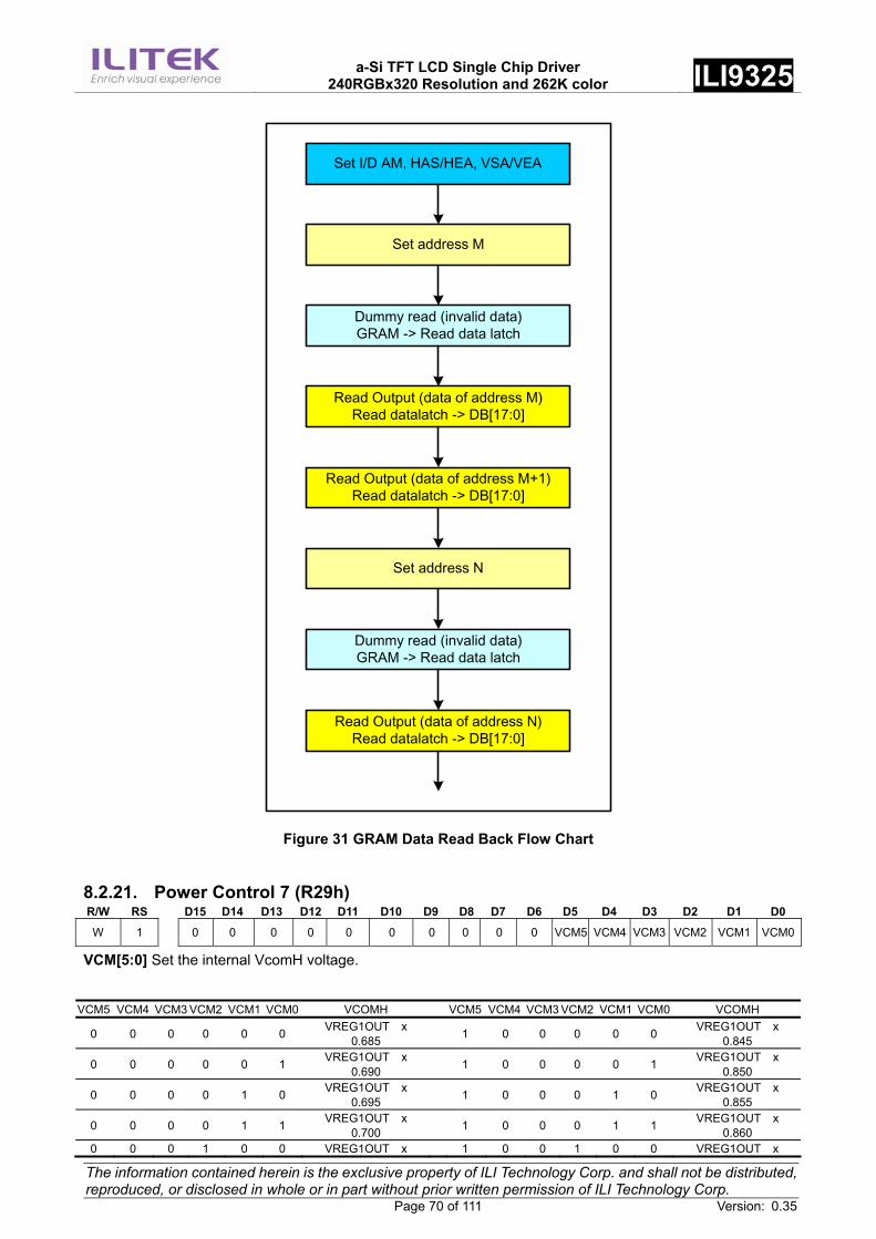
a-Si TFT LCD Single Chip Driver
240RGBx320 Resolution and 262K color ILI9325
The information contained herein is the exclusive property of ILI Technology Corp. and shall not be distributed, reproduced, or disclosed in whole or in part without prior written permission of ILI Technology Corp. Page 70 of 111 Version: 0.35
Set I/D AM, HAS/HEA, VSA/VEA
Set address M
Dummy read (invalid data)GRAM -> Read data latch
Read Output (data of address M)Read datalatch -> DB[17:0]
Set address N
Dummy read (invalid data)GRAM -> Read data latch
Read Output (data of address N)Read datalatch -> DB[17:0]
Read Output (data of address M+1)Read datalatch -> DB[17:0]
Figure 31 GRAM Data Read Back Flow Chart
8.2.21. Power Control 7 (R29h) R/W RS D15 D14 D13 D12 D11 D10 D9 D8 D7 D6 D5 D4 D3 D2 D1 D0
W 1 0 0 0 0 0 0 0 0 0 0 VCM5 VCM4 VCM3 VCM2 VCM1 VCM0
VCM[5:0] Set the internal VcomH voltage.
VCM5 VCM4 VCM3 VCM2 VCM1 VCM0 VCOMH VCM5 VCM4 VCM3 VCM2 VCM1 VCM0 VCOMH
0 0 0 0 0 0 VREG1OUT x 0.685 1 0 0 0 0 0 VREG1OUT x
0.845
0 0 0 0 0 1 VREG1OUT x 0.690 1 0 0 0 0 1 VREG1OUT x
0.850
0 0 0 0 1 0 VREG1OUT x 0.695 1 0 0 0 1 0 VREG1OUT x
0.855
0 0 0 0 1 1 VREG1OUT x 0.700 1 0 0 0 1 1 VREG1OUT x
0.860 0 0 0 1 0 0 VREG1OUT x 1 0 0 1 0 0 VREG1OUT x
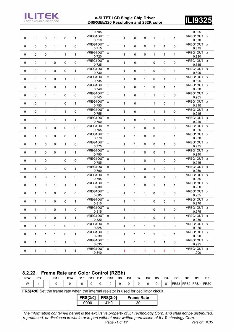
a-Si TFT LCD Single Chip Driver
240RGBx320 Resolution and 262K color ILI9325
The information contained herein is the exclusive property of ILI Technology Corp. and shall not be distributed, reproduced, or disclosed in whole or in part without prior written permission of ILI Technology Corp. Page 71 of 111 Version: 0.35
0.705 0.865
0 0 0 1 0 1 VREG1OUT x 0.710 1 0 0 1 0 1 VREG1OUT x
0.870
0 0 0 1 1 0 VREG1OUT x 0.715 1 0 0 1 1 0 VREG1OUT x
0.875
0 0 0 1 1 1 VREG1OUT x 0.720 1 0 0 1 1 1 VREG1OUT x
0.880
0 0 1 0 0 0 VREG1OUT x 0.725 1 0 1 0 0 0 VREG1OUT x
0.885
0 0 1 0 0 1 VREG1OUT x 0.730 1 0 1 0 0 1 VREG1OUT x
0.890
0 0 1 0 1 0 VREG1OUT x 0.735 1 0 1 0 1 0 VREG1OUT x
0.895
0 0 1 0 1 1 VREG1OUT x 0.740 1 0 1 0 1 1 VREG1OUT x
0.900
0 0 1 1 0 0 VREG1OUT x 0.745 1 0 1 1 0 0 VREG1OUT x
0.905
0 0 1 1 0 1 VREG1OUT x 0.750 1 0 1 1 0 1 VREG1OUT x
0.910
0 0 1 1 1 0 VREG1OUT x 0.755 1 0 1 1 1 0 VREG1OUT x
0.915
0 0 1 1 1 1 VREG1OUT x 0.760 1 0 1 1 1 1 VREG1OUT x
0.920
0 1 0 0 0 0 VREG1OUT x 0.765 1 1 0 0 0 0 VREG1OUT x
0.925
0 1 0 0 0 1 VREG1OUT x 0.770 1 1 0 0 0 1 VREG1OUT x
0.930
0 1 0 0 1 0 VREG1OUT x 0.775 1 1 0 0 1 0 VREG1OUT x
0.935
0 1 0 0 1 1 VREG1OUT x 0.780 1 1 0 0 1 1 VREG1OUT x
0.940
0 1 0 1 0 0 VREG1OUT x 0.785 1 1 0 1 0 0 VREG1OUT x
0.945
0 1 0 1 0 1 VREG1OUT x 0.790 1 1 0 1 0 1 VREG1OUT x
0.950
0 1 0 1 1 0 VREG1OUT x 0.795 1 1 0 1 1 0 VREG1OUT x
0.955
0 1 0 1 1 1 VREG1OUT x 0.800 1 1 0 1 1 1 VREG1OUT x
0.960
0 1 1 0 0 0 VREG1OUT x 0.805 1 1 1 0 0 0 VREG1OUT x
0.965
0 1 1 0 0 1 VREG1OUT x 0.810 1 1 1 0 0 1 VREG1OUT x
0.970
0 1 1 0 1 0 VREG1OUT x 0.815 1 1 1 0 1 0 VREG1OUT x
0.975
0 1 1 0 1 1 VREG1OUT x 0.820 1 1 1 0 1 1 VREG1OUT x
0.980
0 1 1 1 0 0 VREG1OUT x 0.825 1 1 1 1 0 0 VREG1OUT x
0.985
0 1 1 1 0 1 VREG1OUT x 0.830 1 1 1 1 0 1 VREG1OUT x
0.990
0 1 1 1 1 0 VREG1OUT x 0.835 1 1 1 1 1 0 VREG1OUT x
0.995
0 1 1 1 1 1 VREG1OUT x 0.840 1 1 1 1 1 1 VREG1OUT x
1.000
8.2.22. Frame Rate and Color Control (R2Bh) R/W RS D15 D14 D13 D12 D11 D10 D9 D8 D7 D6 D5 D4 D3 D2 D1 D0
W 1 0 0 0 0 0 0 0 0 0 0 0 0 FRS3 FRS2 FRS1 FRS0
FRS[4:0] Set the frame rate when the internal resistor is used for oscillator circuit.
FRS[3:0] FRS[3:0] Frame Rate 0000 4’h0 30
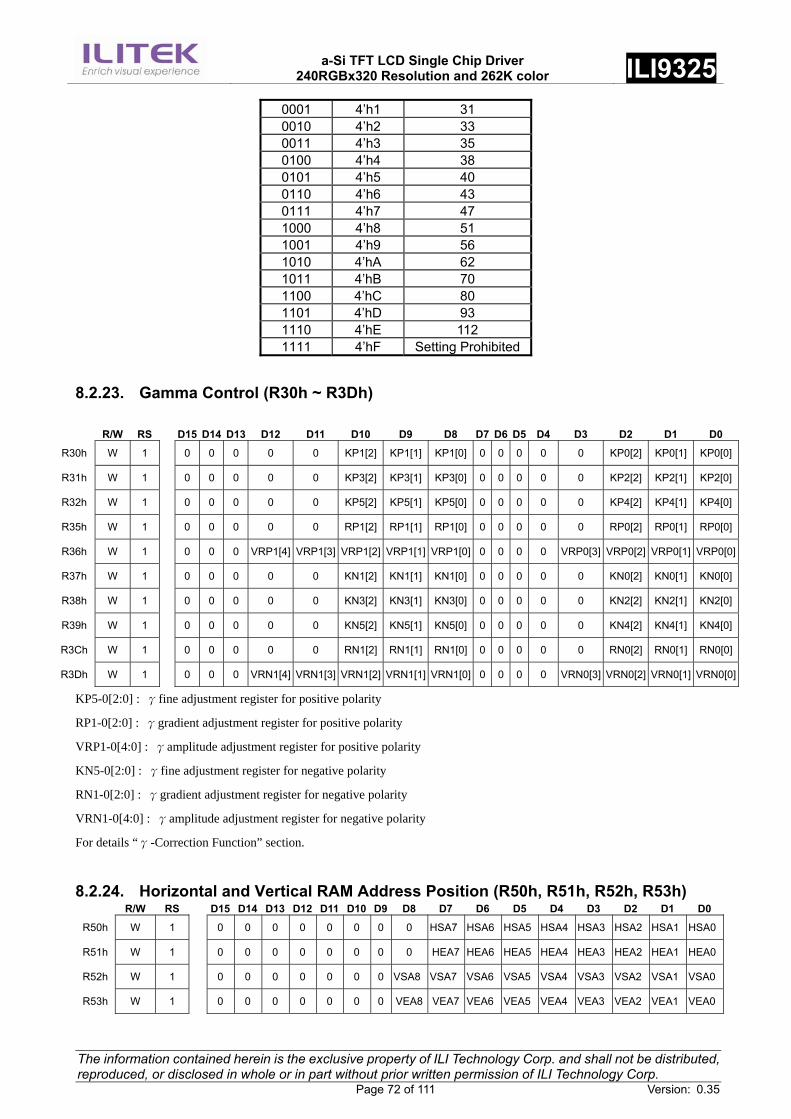
a-Si TFT LCD Single Chip Driver
240RGBx320 Resolution and 262K color ILI9325
The information contained herein is the exclusive property of ILI Technology Corp. and shall not be distributed, reproduced, or disclosed in whole or in part without prior written permission of ILI Technology Corp. Page 72 of 111 Version: 0.35
0001 4’h1 31 0010 4’h2 33 0011 4’h3 35 0100 4’h4 38 0101 4’h5 40 0110 4’h6 43 0111 4’h7 47 1000 4’h8 51 1001 4’h9 56 1010 4’hA 62 1011 4’hB 70 1100 4’hC 80 1101 4’hD 93 1110 4’hE 112 1111 4’hF Setting Prohibited
8.2.23. Gamma Control (R30h ~ R3Dh) R/W RS D15 D14 D13 D12 D11 D10 D9 D8 D7 D6 D5 D4 D3 D2 D1 D0
R30h W 1 0 0 0 0 0 KP1[2] KP1[1] KP1[0] 0 0 0 0 0 KP0[2] KP0[1] KP0[0]
R31h W 1 0 0 0 0 0 KP3[2] KP3[1] KP3[0] 0 0 0 0 0 KP2[2] KP2[1] KP2[0]
R32h W 1 0 0 0 0 0 KP5[2] KP5[1] KP5[0] 0 0 0 0 0 KP4[2] KP4[1] KP4[0]
R35h W 1 0 0 0 0 0 RP1[2] RP1[1] RP1[0] 0 0 0 0 0 RP0[2] RP0[1] RP0[0]
R36h W 1 0 0 0 VRP1[4] VRP1[3] VRP1[2] VRP1[1] VRP1[0] 0 0 0 0 VRP0[3] VRP0[2] VRP0[1] VRP0[0]
R37h W 1 0 0 0 0 0 KN1[2] KN1[1] KN1[0] 0 0 0 0 0 KN0[2] KN0[1] KN0[0]
R38h W 1 0 0 0 0 0 KN3[2] KN3[1] KN3[0] 0 0 0 0 0 KN2[2] KN2[1] KN2[0]
R39h W 1 0 0 0 0 0 KN5[2] KN5[1] KN5[0] 0 0 0 0 0 KN4[2] KN4[1] KN4[0]
R3Ch W 1 0 0 0 0 0 RN1[2] RN1[1] RN1[0] 0 0 0 0 0 RN0[2] RN0[1] RN0[0]
R3Dh W 1 0 0 0 VRN1[4] VRN1[3] VRN1[2] VRN1[1] VRN1[0] 0 0 0 0 VRN0[3] VRN0[2] VRN0[1] VRN0[0]
KP5-0[2:0] : γfine adjustment register for positive polarity
RP1-0[2:0] : γgradient adjustment register for positive polarity
VRP1-0[4:0] : γamplitude adjustment register for positive polarity
KN5-0[2:0] : γfine adjustment register for negative polarity
RN1-0[2:0] : γgradient adjustment register for negative polarity
VRN1-0[4:0] : γamplitude adjustment register for negative polarity
For details “γ-Correction Function” section.
8.2.24. Horizontal and Vertical RAM Address Position (R50h, R51h, R52h, R53h) R/W RS D15 D14 D13 D12 D11 D10 D9 D8 D7 D6 D5 D4 D3 D2 D1 D0
R50h W 1 0 0 0 0 0 0 0 0 HSA7 HSA6 HSA5 HSA4 HSA3 HSA2 HSA1 HSA0
R51h W 1 0 0 0 0 0 0 0 0 HEA7 HEA6 HEA5 HEA4 HEA3 HEA2 HEA1 HEA0
R52h W 1 0 0 0 0 0 0 0 VSA8 VSA7 VSA6 VSA5 VSA4 VSA3 VSA2 VSA1 VSA0
R53h W 1 0 0 0 0 0 0 0 VEA8 VEA7 VEA6 VEA5 VEA4 VEA3 VEA2 VEA1 VEA0
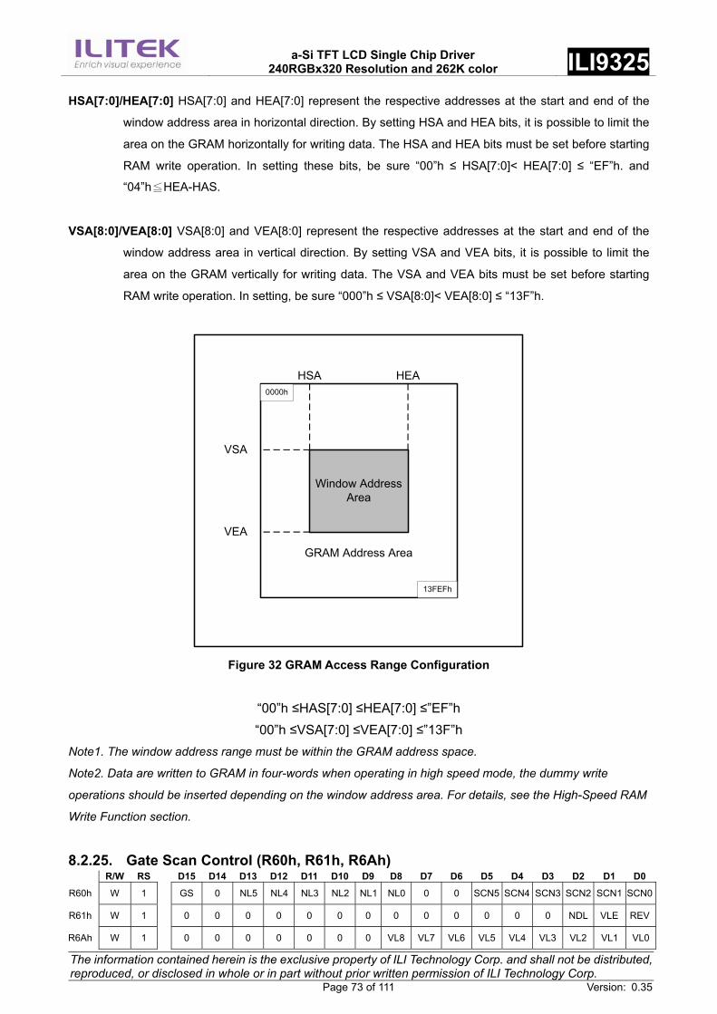
a-Si TFT LCD Single Chip Driver
240RGBx320 Resolution and 262K color ILI9325
The information contained herein is the exclusive property of ILI Technology Corp. and shall not be distributed, reproduced, or disclosed in whole or in part without prior written permission of ILI Technology Corp. Page 73 of 111 Version: 0.35
HSA[7:0]/HEA[7:0] HSA[7:0] and HEA[7:0] represent the respective addresses at the start and end of the
window address area in horizontal direction. By setting HSA and HEA bits, it is possible to limit the
area on the GRAM horizontally for writing data. The HSA and HEA bits must be set before starting
RAM write operation. In setting these bits, be sure “00”h ≤ HSA[7:0]< HEA[7:0] ≤ “EF”h. and
“04”h≦HEA-HAS.
VSA[8:0]/VEA[8:0] VSA[8:0] and VEA[8:0] represent the respective addresses at the start and end of the
window address area in vertical direction. By setting VSA and VEA bits, it is possible to limit the
area on the GRAM vertically for writing data. The VSA and VEA bits must be set before starting
RAM write operation. In setting, be sure “000”h ≤ VSA[8:0]< VEA[8:0] ≤ “13F”h.
Window Address Area
HSA HEA
VSA
VEA
0000h
13FEFh
GRAM Address Area
Figure 32 GRAM Access Range Configuration
“00”h ≤HAS[7:0] ≤HEA[7:0] ≤”EF”h “00”h ≤VSA[7:0] ≤VEA[7:0] ≤”13F”h
Note1. The window address range must be within the GRAM address space.
Note2. Data are written to GRAM in four-words when operating in high speed mode, the dummy write
operations should be inserted depending on the window address area. For details, see the High-Speed RAM
Write Function section.
8.2.25. Gate Scan Control (R60h, R61h, R6Ah) R/W RS D15 D14 D13 D12 D11 D10 D9 D8 D7 D6 D5 D4 D3 D2 D1 D0
R60h W 1 GS 0 NL5 NL4 NL3 NL2 NL1 NL0 0 0 SCN5 SCN4 SCN3 SCN2 SCN1 SCN0
R61h W 1 0 0 0 0 0 0 0 0 0 0 0 0 0 NDL VLE REV
R6Ah W 1 0 0 0 0 0 0 0 VL8 VL7 VL6 VL5 VL4 VL3 VL2 VL1 VL0
a-Si TFT LCD Single Chip Driver
240RGBx320 Resolution and 262K color ILI9325
The information contained herein is the exclusive property of ILI Technology Corp. and shall not be distributed, reproduced, or disclosed in whole or in part without prior written permission of ILI Technology Corp. Page 74 of 111 Version: 0.35
SCN[5:0] The ILI9325 allows to specify the gate line from which the gate driver starts to scan by setting the
SCN[5:0] bits.
Scanning Start Position SM=0 SM=1 SCN[5:0]
GS=0 GS=1 GS=0 GS=1 00h G1 G320 G1 G320 01h G9 G312 G17 G304 02h G17 G304 G33 G288 03h G25 G296 G49 G272 04h G33 G288 G65 G256 05h G41 G280 G81 G240 06h G49 G272 G97 G224 07h G57 G264 G113 G208 08h G65 G256 G129 G192 09h G73 G248 G145 G176 0Ah G81 G240 G161 G160 0Bh G89 G232 G177 G144 0Ch G97 G224 G193 G128 0Dh G105 G216 G209 G112 0Eh G113 G208 G2 G96 0Fh G121 G200 G18 G80 10h G129 G192 G34 G64 11h G137 G184 G50 G48 12h G145 G176 G66 G32 13h G153 G168 G82 G16 14h G161 G160 G98 G319 15h G169 G152 G114 G303 16h G177 G144 G130 G287 17h G185 G136 G146 G271 18h G193 G128 G162 G255 19h G201 G120 G178 G239 1Ah G209 G112 G194 G223 1Bh G217 G104 G114 G207 1Ch G225 G96 G130 G191 1Dh G233 G88 G146 G175 1Eh G241 G80 G162 G159 1Fh G249 G72 G178 G143 20h G257 G64 G194 G127 21h G265 G56 G210 G111 22h G273 G48 G226 G95 23h G281 G40 G242 G79 24h G289 G32 G258 G63 25h G297 G24 G274 G47 26h G305 G16 G290 G31 27h G313 G8 G306 G15
28h ~ 3Fh Setting disabled Setting disabled Setting disabled Setting disabled
NL[5:0]: Sets the number of lines to drive the LCD at an interval of 8 lines. The GRAM address mapping is
not affected by the number of lines set by NL[5:0]. The number of lines must be the same or more
than the number of lines necessary for the size of the liquid crystal panel.
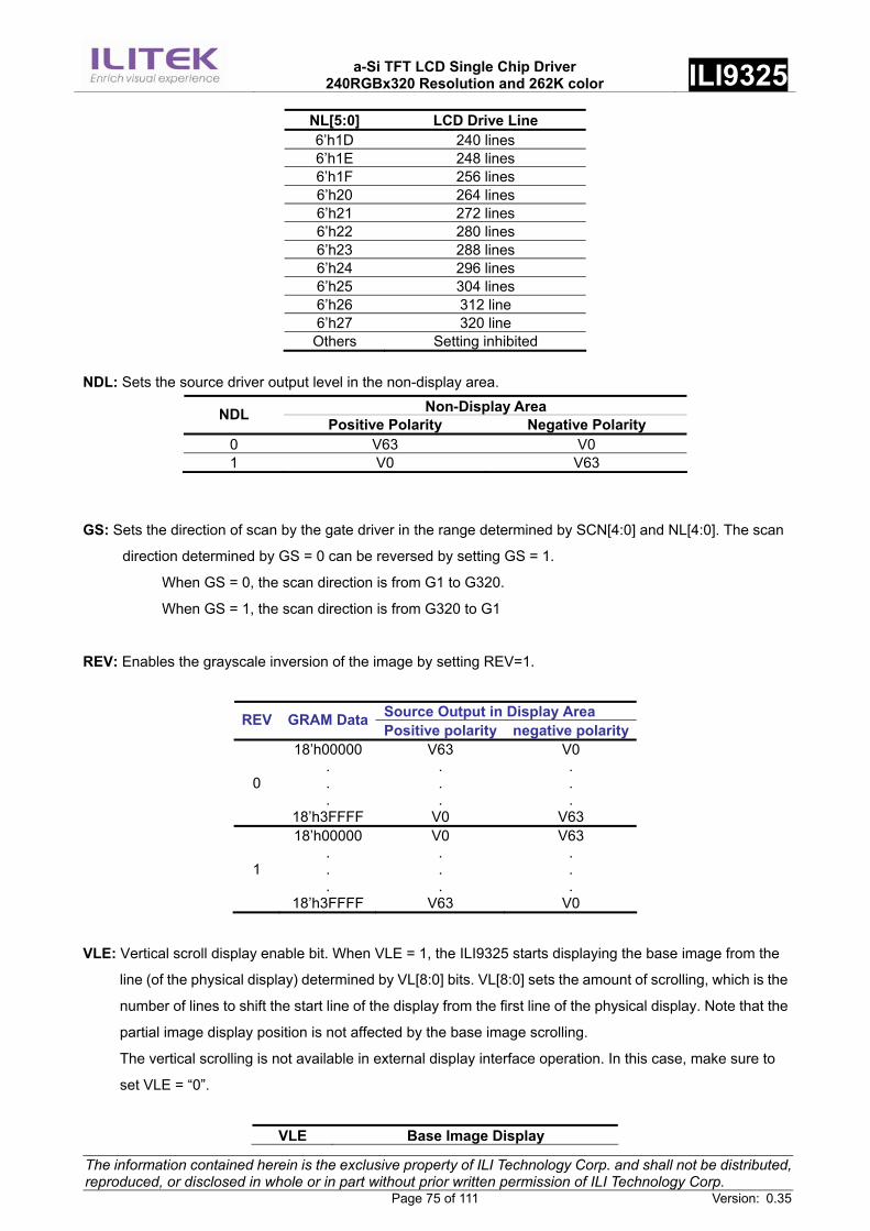
a-Si TFT LCD Single Chip Driver
240RGBx320 Resolution and 262K color ILI9325
The information contained herein is the exclusive property of ILI Technology Corp. and shall not be distributed, reproduced, or disclosed in whole or in part without prior written permission of ILI Technology Corp. Page 75 of 111 Version: 0.35
NL[5:0] LCD Drive Line 6’h1D 240 lines 6’h1E 248 lines 6’h1F 256 lines 6’h20 264 lines 6’h21 272 lines 6’h22 280 lines 6’h23 288 lines 6’h24 296 lines 6’h25 304 lines 6’h26 312 line 6’h27 320 line Others Setting inhibited
NDL: Sets the source driver output level in the non-display area.
Non-Display Area NDL Positive Polarity Negative Polarity
0 V63 V0 1 V0 V63
GS: Sets the direction of scan by the gate driver in the range determined by SCN[4:0] and NL[4:0]. The scan
direction determined by GS = 0 can be reversed by setting GS = 1.
When GS = 0, the scan direction is from G1 to G320.
When GS = 1, the scan direction is from G320 to G1
REV: Enables the grayscale inversion of the image by setting REV=1.
Source Output in Display Area REV GRAM DataPositive polarity negative polarity
0
18’h00000 . . .
18’h3FFFF
V63 . . .
V0
V0 . . .
V63
1
18’h00000 . . .
18’h3FFFF
V0 . . .
V63
V63 . . .
V0
VLE: Vertical scroll display enable bit. When VLE = 1, the ILI9325 starts displaying the base image from the
line (of the physical display) determined by VL[8:0] bits. VL[8:0] sets the amount of scrolling, which is the
number of lines to shift the start line of the display from the first line of the physical display. Note that the
partial image display position is not affected by the base image scrolling.
The vertical scrolling is not available in external display interface operation. In this case, make sure to
set VLE = “0”.
VLE Base Image Display
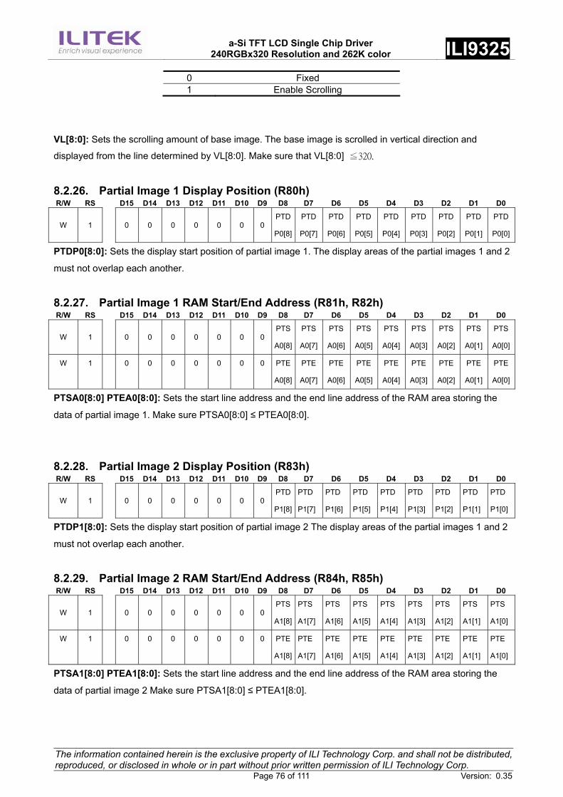
a-Si TFT LCD Single Chip Driver
240RGBx320 Resolution and 262K color ILI9325
The information contained herein is the exclusive property of ILI Technology Corp. and shall not be distributed, reproduced, or disclosed in whole or in part without prior written permission of ILI Technology Corp. Page 76 of 111 Version: 0.35
0 Fixed 1 Enable Scrolling
VL[8:0]: Sets the scrolling amount of base image. The base image is scrolled in vertical direction and
displayed from the line determined by VL[8:0]. Make sure that VL[8:0] ≦320.
8.2.26. Partial Image 1 Display Position (R80h) R/W RS D15 D14 D13 D12 D11 D10 D9 D8 D7 D6 D5 D4 D3 D2 D1 D0
W 1 0 0 0 0 0 0 0PTD
P0[8]
PTD
P0[7]
PTD
P0[6]
PTD
P0[5]
PTD
P0[4]
PTD
P0[3]
PTD
P0[2]
PTD
P0[1]
PTD
P0[0]
PTDP0[8:0]: Sets the display start position of partial image 1. The display areas of the partial images 1 and 2
must not overlap each another.
8.2.27. Partial Image 1 RAM Start/End Address (R81h, R82h) R/W RS D15 D14 D13 D12 D11 D10 D9 D8 D7 D6 D5 D4 D3 D2 D1 D0
W 1 0 0 0 0 0 0 0PTS
A0[8]
PTS
A0[7]
PTS
A0[6]
PTS
A0[5]
PTS
A0[4]
PTS
A0[3]
PTS
A0[2]
PTS
A0[1]
PTS
A0[0]
W 1 0 0 0 0 0 0 0 PTE
A0[8]
PTE
A0[7]
PTE
A0[6]
PTE
A0[5]
PTE
A0[4]
PTE
A0[3]
PTE
A0[2]
PTE
A0[1]
PTE
A0[0]
PTSA0[8:0] PTEA0[8:0]: Sets the start line address and the end line address of the RAM area storing the
data of partial image 1. Make sure PTSA0[8:0] ≤ PTEA0[8:0].
8.2.28. Partial Image 2 Display Position (R83h) R/W RS D15 D14 D13 D12 D11 D10 D9 D8 D7 D6 D5 D4 D3 D2 D1 D0
W 1 0 0 0 0 0 0 0PTD
P1[8]
PTD
P1[7]
PTD
P1[6]
PTD
P1[5]
PTD
P1[4]
PTD
P1[3]
PTD
P1[2]
PTD
P1[1]
PTD
P1[0]
PTDP1[8:0]: Sets the display start position of partial image 2 The display areas of the partial images 1 and 2
must not overlap each another.
8.2.29. Partial Image 2 RAM Start/End Address (R84h, R85h) R/W RS D15 D14 D13 D12 D11 D10 D9 D8 D7 D6 D5 D4 D3 D2 D1 D0
W 1 0 0 0 0 0 0 0PTS
A1[8]
PTS
A1[7]
PTS
A1[6]
PTS
A1[5]
PTS
A1[4]
PTS
A1[3]
PTS
A1[2]
PTS
A1[1]
PTS
A1[0]
W 1 0 0 0 0 0 0 0 PTE
A1[8]
PTE
A1[7]
PTE
A1[6]
PTE
A1[5]
PTE
A1[4]
PTE
A1[3]
PTE
A1[2]
PTE
A1[1]
PTE
A1[0]
PTSA1[8:0] PTEA1[8:0]: Sets the start line address and the end line address of the RAM area storing the
data of partial image 2 Make sure PTSA1[8:0] ≤ PTEA1[8:0].
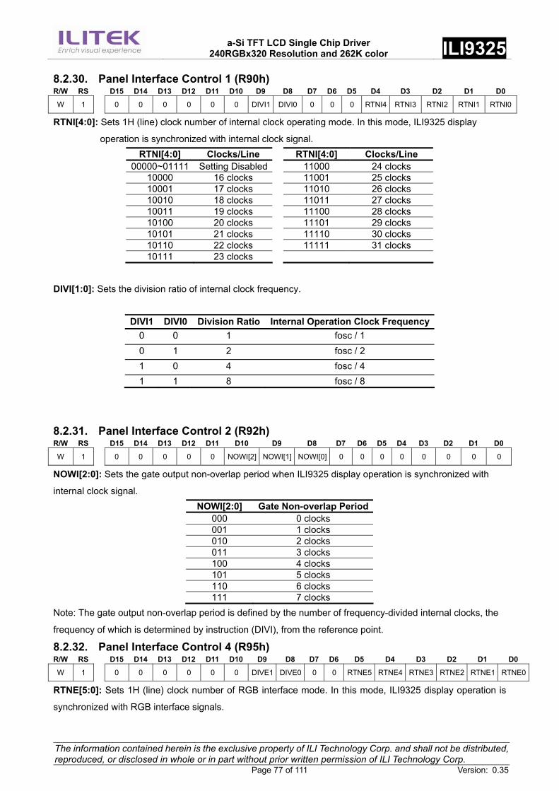
a-Si TFT LCD Single Chip Driver
240RGBx320 Resolution and 262K color ILI9325
The information contained herein is the exclusive property of ILI Technology Corp. and shall not be distributed, reproduced, or disclosed in whole or in part without prior written permission of ILI Technology Corp. Page 77 of 111 Version: 0.35
8.2.30. Panel Interface Control 1 (R90h) R/W RS D15 D14 D13 D12 D11 D10 D9 D8 D7 D6 D5 D4 D3 D2 D1 D0
W 1 0 0 0 0 0 0 DIVI1 DIVI0 0 0 0 RTNI4 RTNI3 RTNI2 RTNI1 RTNI0
RTNI[4:0]: Sets 1H (line) clock number of internal clock operating mode. In this mode, ILI9325 display
operation is synchronized with internal clock signal. RTNI[4:0] Clocks/Line RTNI[4:0] Clocks/Line
00000~01111 Setting Disabled 11000 24 clocks 10000 16 clocks 11001 25 clocks 10001 17 clocks 11010 26 clocks 10010 18 clocks 11011 27 clocks 10011 19 clocks 11100 28 clocks 10100 20 clocks 11101 29 clocks 10101 21 clocks 11110 30 clocks 10110 22 clocks 11111 31 clocks 10111 23 clocks
DIVI[1:0]: Sets the division ratio of internal clock frequency.
DIVI1 DIVI0 Division Ratio Internal Operation Clock Frequency 0 0 1 fosc / 1 0 1 2 fosc / 2 1 0 4 fosc / 4 1 1 8 fosc / 8
8.2.31. Panel Interface Control 2 (R92h) R/W RS D15 D14 D13 D12 D11 D10 D9 D8 D7 D6 D5 D4 D3 D2 D1 D0
W 1 0 0 0 0 0 NOWI[2] NOWI[1] NOWI[0] 0 0 0 0 0 0 0 0
NOWI[2:0]: Sets the gate output non-overlap period when ILI9325 display operation is synchronized with
internal clock signal. NOWI[2:0] Gate Non-overlap Period
000 0 clocks 001 1 clocks 010 2 clocks 011 3 clocks 100 4 clocks 101 5 clocks 110 6 clocks 111 7 clocks
Note: The gate output non-overlap period is defined by the number of frequency-divided internal clocks, the
frequency of which is determined by instruction (DIVI), from the reference point.
8.2.32. Panel Interface Control 4 (R95h) R/W RS D15 D14 D13 D12 D11 D10 D9 D8 D7 D6 D5 D4 D3 D2 D1 D0
W 1 0 0 0 0 0 0 DIVE1 DIVE0 0 0 RTNE5 RTNE4 RTNE3 RTNE2 RTNE1 RTNE0
RTNE[5:0]: Sets 1H (line) clock number of RGB interface mode. In this mode, ILI9325 display operation is
synchronized with RGB interface signals.
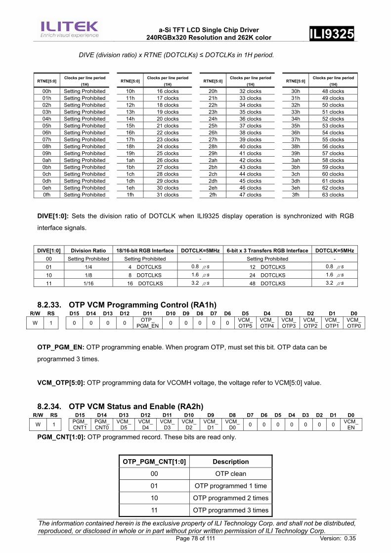
a-Si TFT LCD Single Chip Driver
240RGBx320 Resolution and 262K color ILI9325
The information contained herein is the exclusive property of ILI Technology Corp. and shall not be distributed, reproduced, or disclosed in whole or in part without prior written permission of ILI Technology Corp. Page 78 of 111 Version: 0.35
DIVE (division ratio) x RTNE (DOTCLKs) ≤ DOTCLKs in 1H period.
RTNE[5:0] Clocks per line period
(1H) RTNE[5:0]
Clocks per line period (1H)
RTNE[5:0]Clocks per line period
(1H) RTNE[5:0]
Clocks per line period (1H)
00h Setting Prohibited 10h 16 clocks 20h 32 clocks 30h 48 clocks 01h Setting Prohibited 11h 17 clocks 21h 33 clocks 31h 49 clocks 02h Setting Prohibited 12h 18 clocks 22h 34 clocks 32h 50 clocks 03h Setting Prohibited 13h 19 clocks 23h 35 clocks 33h 51 clocks 04h Setting Prohibited 14h 20 clocks 24h 36 clocks 34h 52 clocks 05h Setting Prohibited 15h 21 clocks 25h 37 clocks 35h 53 clocks 06h Setting Prohibited 16h 22 clocks 26h 38 clocks 36h 54 clocks 07h Setting Prohibited 17h 23 clocks 27h 39 clocks 37h 55 clocks 08h Setting Prohibited 18h 24 clocks 28h 40 clocks 38h 56 clocks 09h Setting Prohibited 19h 25 clocks 29h 41 clocks 39h 57 clocks 0ah Setting Prohibited 1ah 26 clocks 2ah 42 clocks 3ah 58 clocks 0bh Setting Prohibited 1bh 27 clocks 2bh 43 clocks 3bh 59 clocks 0ch Setting Prohibited 1ch 28 clocks 2ch 44 clocks 3ch 60 clocks 0dh Setting Prohibited 1dh 29 clocks 2dh 45 clocks 3dh 61 clocks 0eh Setting Prohibited 1eh 30 clocks 2eh 46 clocks 3eh 62 clocks 0fh Setting Prohibited 1fh 31 clocks 2fh 47 clocks 3fh 63 clocks
DIVE[1:0]: Sets the division ratio of DOTCLK when ILI9325 display operation is synchronized with RGB
interface signals.
DIVE[1:0] Division Ratio 18/16-bit RGB Interface DOTCLK=5MHz 6-bit x 3 Transfers RGB Interface DOTCLK=5MHz
00 Setting Prohibited Setting Prohibited - Setting Prohibited - 01 1/4 4 DOTCLKS 0.8 μs 12 DOTCLKS 0.8 μs
10 1/8 8 DOTCLKS 1.6 μs 24 DOTCLKS 1.6 μs
11 1/16 16 DOTCLKS 3.2 μs 48 DOTCLKS 3.2 μs
8.2.33. OTP VCM Programming Control (RA1h) R/W RS D15 D14 D13 D12 D11 D10 D9 D8 D7 D6 D5 D4 D3 D2 D1 D0
W 1 0 0 0 0 OTP_ PGM_EN 0 0 0 0 0 VCM_
OTP5VCM_OTP4
VCM_ OTP3
VCM_ OTP2
VCM_OTP1
VCM_OTP0
OTP_PGM_EN: OTP programming enable. When program OTP, must set this bit. OTP data can be
programmed 3 times.
VCM_OTP[5:0]: OTP programming data for VCOMH voltage, the voltage refer to VCM[5:0] value.
8.2.34. OTP VCM Status and Enable (RA2h) R/W RS D15 D14 D13 D12 D11 D10 D9 D8 D7 D6 D5 D4 D3 D2 D1 D0
W 1 PGM_ CNT1
PGM_ CNT0
VCM_ D5
VCM_ D4
VCM_D3
VCM_D2
VCM_D1
VCM_D0 0 0 0 0 0 0 0 VCM_
EN
PGM_CNT[1:0]: OTP programmed record. These bits are read only.
OTP_PGM_CNT[1:0] Description
00 OTP clean
01 OTP programmed 1 time
10 OTP programmed 2 times
11 OTP programmed 3 times
a-Si TFT LCD Single Chip Driver
240RGBx320 Resolution and 262K color ILI9325
The information contained herein is the exclusive property of ILI Technology Corp. and shall not be distributed, reproduced, or disclosed in whole or in part without prior written permission of ILI Technology Corp. Page 79 of 111 Version: 0.35
VCM_D[5:0]: OTP VCM data read value. These bits are read only.
VCM_EN: OTP VCM data enable.
’1’: Set this bit to enable OTP VCM data to replace R29h VCM value.
’0’: Default value, use R29h VCM value.
8.2.35. OTP Programming ID Key (RA5h) R/W RS D15 D14 D13 D12 D11 D10 D9 D8 D7 D6 D5 D4 D3 D2 D1 D0
W 1 KEY 15
KEY 14
KEY 13
KEY 12
KEY 11
KEY10
KEY9
KEY8
KEY7
KEY6
KEY5
KEY 4
KEY 3
KEY 2
KEY1
KEY0
KEY[15:0]: OTP Programming ID key protection. Before writing OTP programming data RA1h, it must write
RA5h with 0xAA55 value first to make OTP programming successfully. If RA5h is not written with
0xAA55, OTP programming will be fail. See OTP Programming flow.
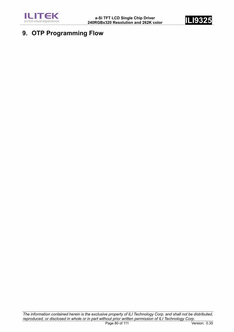
a-Si TFT LCD Single Chip Driver
240RGBx320 Resolution and 262K color ILI9325
The information contained herein is the exclusive property of ILI Technology Corp. and shall not be distributed, reproduced, or disclosed in whole or in part without prior written permission of ILI Technology Corp. Page 80 of 111 Version: 0.35
9. OTP Programming Flow
a-Si TFT LCD Single Chip Driver
240RGBx320 Resolution and 262K color ILI9325
The information contained herein is the exclusive property of ILI Technology Corp. and shall not be distributed, reproduced, or disclosed in whole or in part without prior written permission of ILI Technology Corp. Page 81 of 111 Version: 0.35
N
Start
Power On ILI9325
CheckOTP_PGM_CNT=11?
Supply External7.0V to DDVDH
Wait 10ms
Set ID KeyRA5h=0xAA55
Program OTP VCM DataRA1h=0x08xx
(xx=6 bit VCM value)
Wait 10ms
Cut Off External7.0V Power
Reset
End
Y

a-Si TFT LCD Single Chip Driver
240RGBx320 Resolution and 262K color ILI9325
The information contained herein is the exclusive property of ILI Technology Corp. and shall not be distributed, reproduced, or disclosed in whole or in part without prior written permission of ILI Technology Corp. Page 82 of 111 Version: 0.35
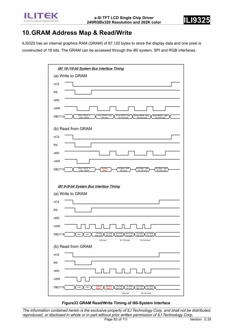
a-Si TFT LCD Single Chip Driver
240RGBx320 Resolution and 262K color ILI9325
The information contained herein is the exclusive property of ILI Technology Corp. and shall not be distributed, reproduced, or disclosed in whole or in part without prior written permission of ILI Technology Corp. Page 83 of 111 Version: 0.35
10. GRAM Address Map & Read/Write ILI9325 has an internal graphics RAM (GRAM) of 87,120 bytes to store the display data and one pixel is
constructed of 18 bits. The GRAM can be accessed through the i80 system, SPI and RGB interfaces.
i80 18-/16-bit System Bus Interface Timing
Write “0022h” to index register
Write GRAM “data”Nth pixel
nWR
DB[17:0]
nRD
RS
nCS
(a) Write to GRAM
nWR
DB[17:0]
nRD
RS
nCS
(b) Read from GRAM
i80 9-/8-bit System Bus Interface Timing
(a) Write to GRAM
(b) Read from GRAM
Write GRAM “data”(N+1)th pixel
Write GRAM “data”(N+2)th pixel
Write GRAM “data”(N+3)th pixel
Write “0022h” to index register
1st Read “data”Nth pixel
Dummy Read
2nd Read “data”(N+1)th pixel
3rd Read “data”(N+2)th pixel
“00h”
Nth pixel
nWR
DB[17:9]
nRD
RS
nCS
“22h” 1st write high byte
1st write low byte
(N+1)th pixel
2nd write high byte
2nd write low byte
(N+2)th pixel
3rd write high byte
3rd write low byte
“00h”
Nth pixel
nWR
DB[17:9]
nRD
RS
nCS
“22h” Dummy Read 1
Dummy Read 2
(N+1)th pixel
1st read high byte
1st read low byte
2nd read high byte
2nd read low byte
Figure33 GRAM Read/Write Timing of i80-System Interface
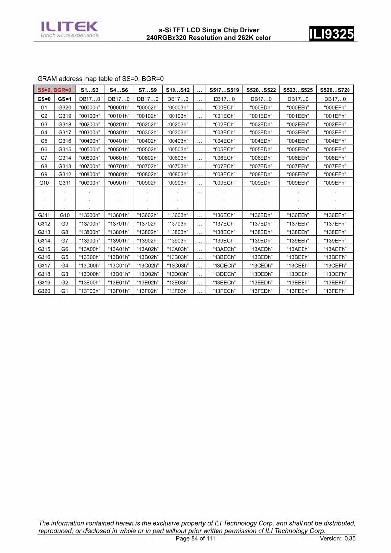
a-Si TFT LCD Single Chip Driver
240RGBx320 Resolution and 262K color ILI9325
The information contained herein is the exclusive property of ILI Technology Corp. and shall not be distributed, reproduced, or disclosed in whole or in part without prior written permission of ILI Technology Corp. Page 84 of 111 Version: 0.35
GRAM address map table of SS=0, BGR=0
SS=0, BGR=0 S1…S3 S4…S6 S7…S9 S10…S12 … S517…S519 S520…S522 S523…S525 S526…S720GS=0 GS=1 DB17…0 DB17…0 DB17…0 DB17…0 … DB17…0 DB17…0 DB17…0 DB17…0
G1 G320 “00000h” “00001h” “00002h” “00003h” … “000ECh” “000EDh” “000EEh” “000EFh” G2 G319 “00100h” “00101h” “00102h” “00103h” … “001ECh” “001EDh” “001EEh” “001EFh” G3 G318 “00200h” “00201h” “00202h” “00203h” … “002ECh” “002EDh” “002EEh” “002EFh” G4 G317 “00300h” “00301h” “00302h” “00303h” … “003ECh” “003EDh” “003EEh” “003EFh” G5 G316 “00400h” “00401h” “00402h” “00403h” … “004ECh” “004EDh” “004EEh” “004EFh” G6 G315 “00500h” “00501h” “00502h” “00503h” … “005ECh” “005EDh” “005EEh” “005EFh” G7 G314 “00600h” “00601h” “00602h” “00603h” … “006ECh” “006EDh” “006EEh” “006EFh” G8 G313 “00700h” “00701h” “00702h” “00703h” … “007ECh” “007EDh” “007EEh” “007EFh” G9 G312 “00800h” “00801h” “00802h” “00803h” … “008ECh” “008EDh” “008EEh” “008EFh”
G10 G311 “00900h” “00901h” “00902h” “00903h” … “009ECh” “009EDh” “009EEh” “009EFh” . . .
.
.
.
.
.
.
.
.
.
.
.
.
.
.
.
… . . .
.
.
.
.
.
.
.
.
. G311 G10 “13600h” “13601h” “13602h” “13603h” … “136ECh” “136EDh” “136EEh” “136EFh” G312 G9 “13700h” “13701h” “13702h” “13703h” … “137ECh” “137EDh” “137EEh” “137EFh” G313 G8 “13800h” “13801h” “13802h” “13803h” … “138ECh” “138EDh” “138EEh” “138EFh” G314 G7 “13900h” “13901h” “13902h” “13903h” … “139ECh” “139EDh” “139EEh” “139EFh” G315 G6 “13A00h” “13A01h” “13A02h” “13A03h” … “13AECh” “13AEDh” “13AEEh” “13AEFh” G316 G5 “13B00h” “13B01h” “13B02h” “13B03h” … “13BECh” “13BEDh” “13BEEh” “13BEFh” G317 G4 “13C00h” “13C01h” “13C02h” “13C03h” … “13CECh” “13CEDh” “13CEEh” “13CEFh” G318 G3 “13D00h” “13D01h” “13D02h” “13D03h” … “13DECh” “13DEDh” “13DEEh” “13DEFh” G319 G2 “13E00h” “13E01h” “13E02h” “13E03h” … “13EECh” “13EEDh” “13EEEh” “13EEFh” G320 G1 “13F00h” “13F01h” “13F02h” “13F03h” … “13FECh” “13FEDh” “13FEEh” “13FEFh”
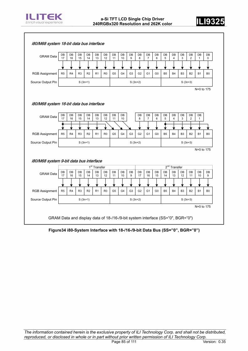
a-Si TFT LCD Single Chip Driver
240RGBx320 Resolution and 262K color ILI9325
The information contained herein is the exclusive property of ILI Technology Corp. and shall not be distributed, reproduced, or disclosed in whole or in part without prior written permission of ILI Technology Corp. Page 85 of 111 Version: 0.35
DB17
DB16
DB15
DB14
DB13
DB12
DB11
DB10
DB8
DB7
DB6
DB5
DB4
DB3
DB2
DB1
i80/M68 system 16-bit data bus interface
GRAM Data
RGB Assignment R5 R4 R3 R2 R1 R0 G5 G4 G2 G1 G0 B5 B4 B3 B2 B1G3
S (3n+1)Source Output Pin S (3n+2) S (3n+3)
N=0 to 175
B0
DB17
DB16
DB15
DB14
DB13
DB12
DB11
DB10
DB9
DB8
DB7
DB6
DB5
DB4
DB3
DB2
DB1
DB0
i80/M68 system 18-bit data bus interface
GRAM Data
RGB Assignment R5 R4 R3 R2 R1 R0 G5 G4 G2 G1 G0 B5 B4 B3 B2 B1G3
S (3n+1)Source Output Pin S (3n+2) S (3n+3)
N=0 to 175
B0
DB17
DB16
DB15
DB14
DB13
DB12
DB11
DB10
DB9
i80/M68 system 9-bit data bus interface
GRAM Data
RGB Assignment R5 R4 R3 R2 R1 R0 G5 G4 G2 G1 G0 B5 B4 B3 B2 B1G3
S (3n+1)Source Output Pin S (3n+2) S (3n+3)
N=0 to 175
B0
DB17
DB16
DB15
DB14
DB13
DB12
DB11
DB10
DB9
1st Transfer 2nd Transfer
GRAM Data and display data of 18-/16-/9-bit system interface (SS=”0", BGR=”0")
Figure34 i80-System Interface with 18-/16-/9-bit Data Bus (SS=”0”, BGR=”0”)
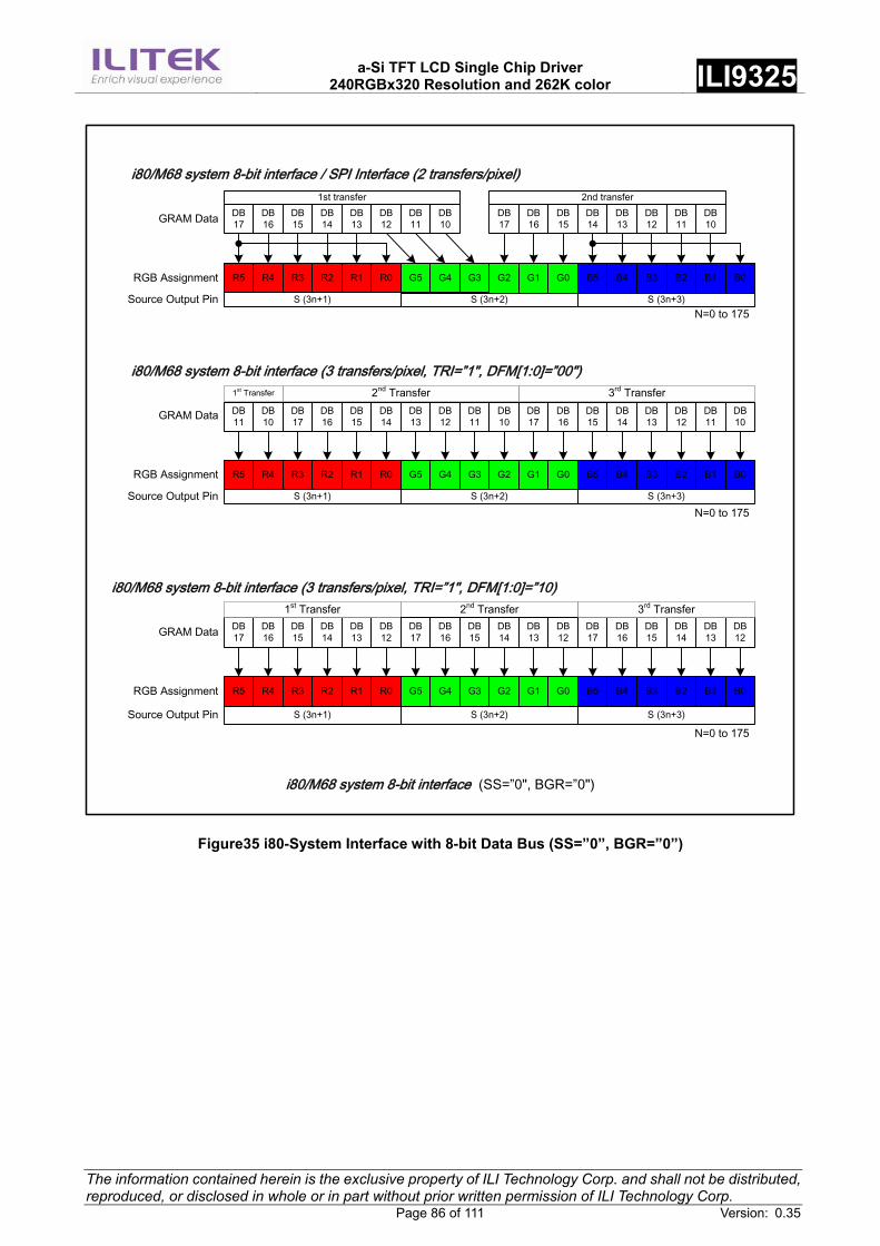
a-Si TFT LCD Single Chip Driver
240RGBx320 Resolution and 262K color ILI9325
The information contained herein is the exclusive property of ILI Technology Corp. and shall not be distributed, reproduced, or disclosed in whole or in part without prior written permission of ILI Technology Corp. Page 86 of 111 Version: 0.35
i80/M68 system 8-bit interface / SPI Interface (2 transfers/pixel)
DB17
DB16
DB15
DB14
DB13
DB12
DB11
DB10GRAM Data
RGB Assignment R5 R4 R3 R2 R1 R0 G5 G4 G2 G1 G0 B5 B4 B3 B2 B1G3
S (3n+1)Source Output Pin S (3n+2) S (3n+3)N=0 to 175
B0
GRAM Data
RGB Assignment
Source Output Pin
i80/M68 system 8-bit interface (SS=”0", BGR=”0")
DB17
DB16
DB15
DB14
DB13
DB12
DB11
DB10
i80/M68 system 8-bit interface (3 transfers/pixel, TRI=”1", DFM[1:0]=”00")
GRAM Data
RGB Assignment R5 R4 R3 R2 R1 R0 G5 G4 G2 G1 G0 B5 B4 B3 B2 B1G3
S (3n+1)Source Output Pin S (3n+2) S (3n+3)
N=0 to 175
B0
1st Transfer 2nd Transfer 3rd Transfer
i80/M68 system 8-bit interface (3 transfers/pixel, TRI=”1", DFM[1:0]=”10)
DB17
DB16
DB15
DB14
DB13
DB12
R5 R4 R3 R2 R1 R0 G5 G4 G2 G1 G0 B5 B4 B3 B2 B1G3
S (3n+1) S (3n+2) S (3n+3)
N=0 to 175
B0
1st Transfer 2nd TransferDB17
DB16
DB15
DB14
DB13
DB12
DB17
DB16
DB15
DB14
DB13
DB12
3rd Transfer
1st transfer 2nd transfer
DB17
DB16
DB15
DB14
DB13
DB12
DB11
DB10
DB17
DB16
DB15
DB14
DB13
DB12
DB11
DB10
DB11
DB10
Figure35 i80-System Interface with 8-bit Data Bus (SS=”0”, BGR=”0”)
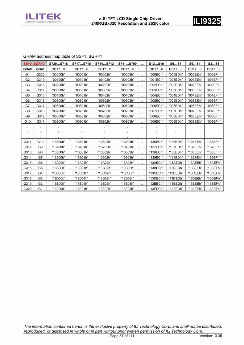
a-Si TFT LCD Single Chip Driver
240RGBx320 Resolution and 262K color ILI9325
The information contained herein is the exclusive property of ILI Technology Corp. and shall not be distributed, reproduced, or disclosed in whole or in part without prior written permission of ILI Technology Corp. Page 87 of 111 Version: 0.35
GRAM address map table of SS=1, BGR=1
SS=0, BGR=0 S720…S718 S717…S715 S714…S712 S711…S709 … S12…S10 S9…S7 S6…S4 S3…S1GS=0 GS=1 DB17…0 DB17…0 DB17…0 DB17…0 … DB17…0 DB17…0 DB17…0 DB17…0
G1 G320 “00000h” “00001h” “00002h” “00003h” … “000ECh” “000EDh” “000EEh” “000EFh”G2 G319 “00100h” “00101h” “00102h” “00103h” … “001ECh” “001EDh” “001EEh” “001EFh”G3 G318 “00200h” “00201h” “00202h” “00203h” … “002ECh” “002EDh” “002EEh” “002EFh”G4 G317 “00300h” “00301h” “00302h” “00303h” … “003ECh” “003EDh” “003EEh” “003EFh”G5 G316 “00400h” “00401h” “00402h” “00403h” … “004ECh” “004EDh” “004EEh” “004EFh”G6 G315 “00500h” “00501h” “00502h” “00503h” … “005ECh” “005EDh” “005EEh” “005EFh”G7 G314 “00600h” “00601h” “00602h” “00603h” … “006ECh” “006EDh” “006EEh” “006EFh”G8 G313 “00700h” “00701h” “00702h” “00703h” … “007ECh” “007EDh” “007EEh” “007EFh”G9 G312 “00800h” “00801h” “00802h” “00803h” … “008ECh” “008EDh” “008EEh” “008EFh”
G10 G311 “00900h” “00901h” “00902h” “00903h” … “009ECh” “009EDh” “009EEh” “009EFh”. . .
.
.
.
.
.
.
.
.
.
.
.
.
.
.
.
… . . .
.
.
.
.
.
.
.
.
. G311 G10 “13600h” “13601h” “13602h” “13603h” … “136ECh” “136EDh” “136EEh” “136EFh”G312 G9 “13700h” “13701h” “13702h” “13703h” … “137ECh” “137EDh” “137EEh” “137EFh”G313 G8 “13800h” “13801h” “13802h” “13803h” … “138ECh” “138EDh” “138EEh” “138EFh”G314 G7 “13900h” “13901h” “13902h” “13903h” … “139ECh” “139EDh” “139EEh” “139EFh”G315 G6 “13A00h” “13A01h” “13A02h” “13A03h” … “13AECh” “13AEDh” “13AEEh” “13AEFh”G316 G5 “13B00h” “13B01h” “13B02h” “13B03h” … “13BECh” “13BEDh” “13BEEh” “13BEFh”G317 G4 “13C00h” “13C01h” “13C02h” “13C03h” … “13CECh” “13CEDh” “13CEEh” “13CEFh”G318 G3 “13D00h” “13D01h” “13D02h” “13D03h” … “13DECh” “13DEDh” “13DEEh” “13DEFh”G319 G2 “13E00h” “13E01h” “13E02h” “13E03h” … “13EECh” “13EEDh” “13EEEh” “13EEFh”G320 G1 “13F00h” “13F01h” “13F02h” “13F03h” … “13FECh” “13FEDh” “13FEEh” “13FEFh”
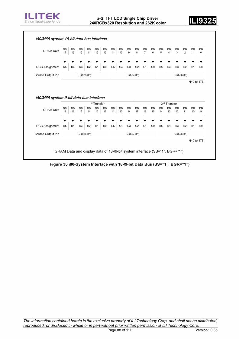
a-Si TFT LCD Single Chip Driver
240RGBx320 Resolution and 262K color ILI9325
The information contained herein is the exclusive property of ILI Technology Corp. and shall not be distributed, reproduced, or disclosed in whole or in part without prior written permission of ILI Technology Corp. Page 88 of 111 Version: 0.35
DB17
DB16
DB15
DB14
DB13
DB12
DB11
DB10
DB9
DB8
DB7
DB6
DB5
DB4
DB3
DB2
DB1
DB0
i80/M68 system 18-bit data bus interface
GRAM Data
RGB Assignment R5 R4 R3 R2 R1 R0 G5 G4 G2 G1 G0 B5 B4 B3 B2 B1G3
S (528-3n)Source Output Pin S (527-3n) S (526-3n)
N=0 to 175
B0
DB17
DB16
DB15
DB14
DB13
DB12
DB11
DB10
DB9
i80/M68 system 9-bit data bus interface
GRAM Data
RGB Assignment R5 R4 R3 R2 R1 R0 G5 G4 G2 G1 G0 B5 B4 B3 B2 B1G3
Source Output Pin
N=0 to 175
B0
DB17
DB16
DB15
DB14
DB13
DB12
DB11
DB10
DB9
1st Transfer 2nd Transfer
GRAM Data and display data of 18-/9-bit system interface (SS=”1", BGR=”1")
S (528-3n) S (527-3n) S (526-3n)
Figure 36 i80-System Interface with 18-/9-bit Data Bus (SS=”1”, BGR=”1”)
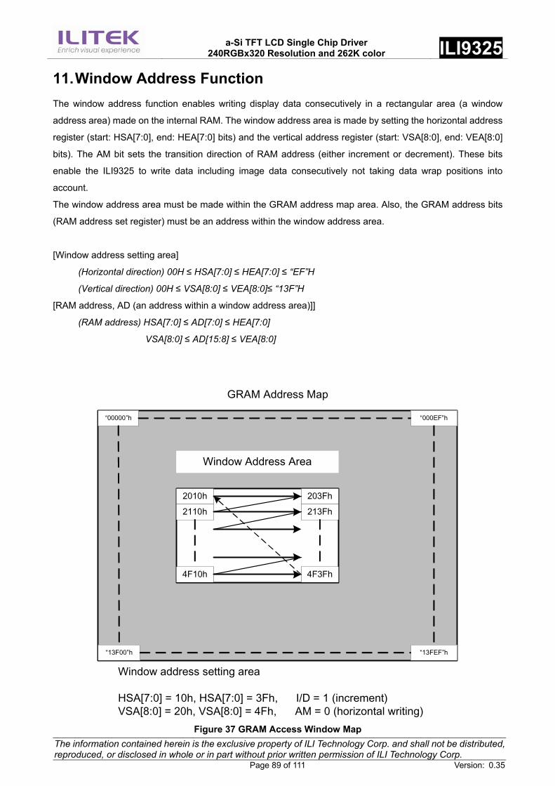
a-Si TFT LCD Single Chip Driver
240RGBx320 Resolution and 262K color ILI9325
The information contained herein is the exclusive property of ILI Technology Corp. and shall not be distributed, reproduced, or disclosed in whole or in part without prior written permission of ILI Technology Corp. Page 89 of 111 Version: 0.35
11. Window Address Function The window address function enables writing display data consecutively in a rectangular area (a window
address area) made on the internal RAM. The window address area is made by setting the horizontal address
register (start: HSA[7:0], end: HEA[7:0] bits) and the vertical address register (start: VSA[8:0], end: VEA[8:0]
bits). The AM bit sets the transition direction of RAM address (either increment or decrement). These bits
enable the ILI9325 to write data including image data consecutively not taking data wrap positions into
account.
The window address area must be made within the GRAM address map area. Also, the GRAM address bits
(RAM address set register) must be an address within the window address area.
[Window address setting area]
(Horizontal direction) 00H ≤ HSA[7:0] ≤ HEA[7:0] ≤ “EF”H
(Vertical direction) 00H ≤ VSA[8:0] ≤ VEA[8:0]≤ “13F”H
[RAM address, AD (an address within a window address area)]]
(RAM address) HSA[7:0] ≤ AD[7:0] ≤ HEA[7:0]
VSA[8:0] ≤ AD[15:8] ≤ VEA[8:0]
“00000”h “000EF”h
“13FEF”h“13F00”h
2010h 203Fh
4F3Fh4F10h
2110h 213Fh
Window Address Area
Window address setting area
HSA[7:0] = 10h, HSA[7:0] = 3Fh, I/D = 1 (increment)VSA[8:0] = 20h, VSA[8:0] = 4Fh, AM = 0 (horizontal writing)
GRAM Address Map
Figure 37 GRAM Access Window Map
a-Si TFT LCD Single Chip Driver
240RGBx320 Resolution and 262K color ILI9325
The information contained herein is the exclusive property of ILI Technology Corp. and shall not be distributed, reproduced, or disclosed in whole or in part without prior written permission of ILI Technology Corp. Page 90 of 111 Version: 0.35
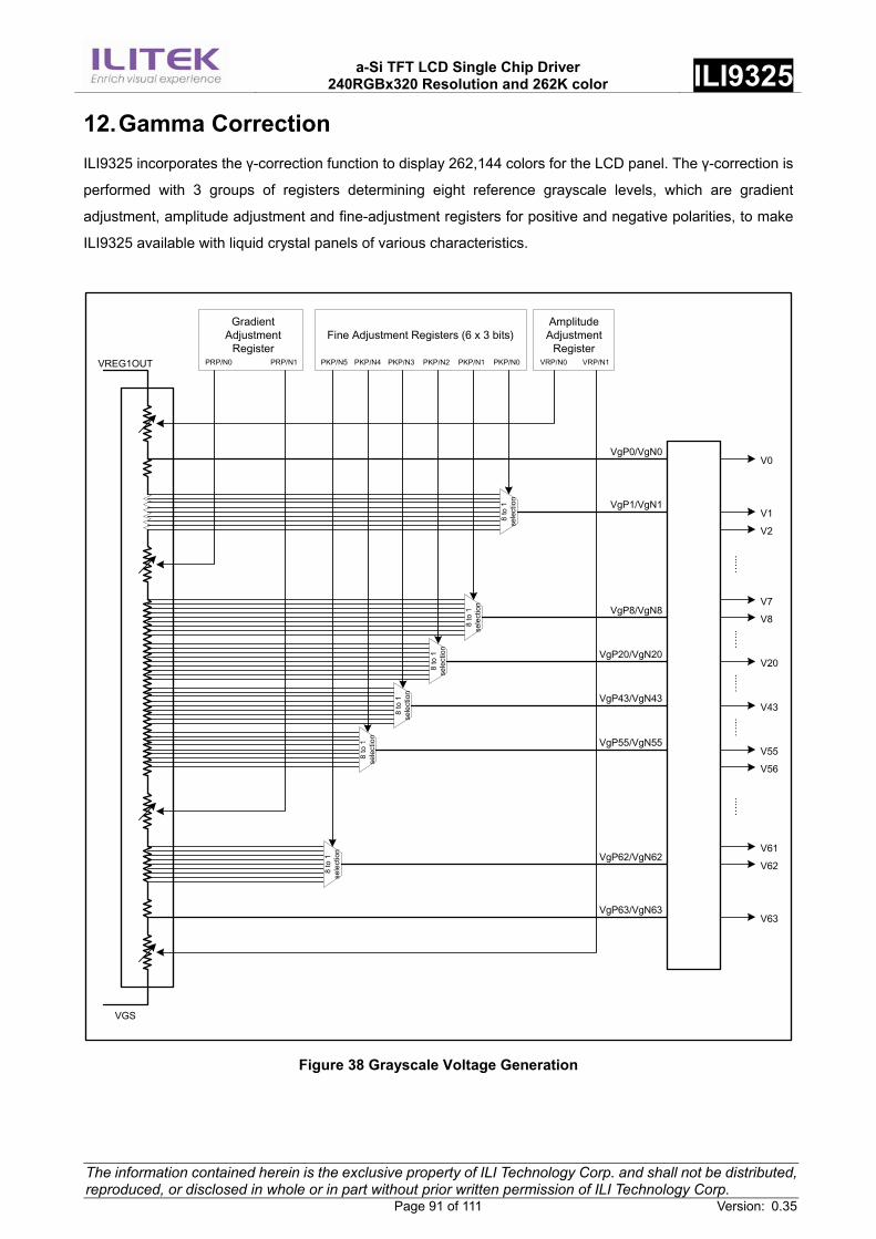
a-Si TFT LCD Single Chip Driver
240RGBx320 Resolution and 262K color ILI9325
The information contained herein is the exclusive property of ILI Technology Corp. and shall not be distributed, reproduced, or disclosed in whole or in part without prior written permission of ILI Technology Corp. Page 91 of 111 Version: 0.35
12. Gamma Correction ILI9325 incorporates the γ-correction function to display 262,144 colors for the LCD panel. The γ-correction is
performed with 3 groups of registers determining eight reference grayscale levels, which are gradient
adjustment, amplitude adjustment and fine-adjustment registers for positive and negative polarities, to make
ILI9325 available with liquid crystal panels of various characteristics.
8 to
1
sele
ctio
n
8 to
1
sele
ctio
n
8 to
1
sele
ctio
n
8 to
1
sele
ctio
n
8 to
1
sele
ctio
n
8 to
1
sele
ctio
n
PRP/N0
Gradient Adjustment
RegisterPRP/N1 VRP/N0
Amplitude Adjustment
RegisterVRP/N1PKP/N5
Fine Adjustment Registers (6 x 3 bits)
VgP0/VgN0
VgP1/VgN1
VgP8/VgN8
VgP20/VgN20
VgP43/VgN43
VgP55/VgN55
VgP62/VgN62
VgP63/VgN63
V0
V1
V8
…...
V2
V7
V20
V43
V55
…...
…...
…...
V62
…...
V63
V61
V56
VREG1OUT
VGS
PKP/N4 PKP/N3 PKP/N2 PKP/N1 PKP/N0
Figure 38 Grayscale Voltage Generation
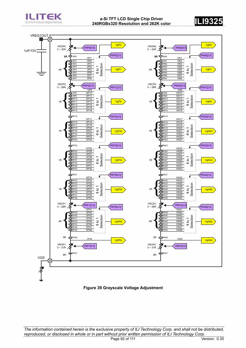
a-Si TFT LCD Single Chip Driver
240RGBx320 Resolution and 262K color ILI9325
The information contained herein is the exclusive property of ILI Technology Corp. and shall not be distributed, reproduced, or disclosed in whole or in part without prior written permission of ILI Technology Corp. Page 92 of 111 Version: 0.35
VgP0
VP1VP2VP3VP4VP5VP6VP7VP8
RP1RP2RP3RP4RP5RP6RP7
RP15
VP25VP26VP27VP28VP29VP30VP31VP32
RP24RP25RP26RP27RP28RP29RP30
RP23
VP33VP34VP35VP36VP37VP38VP39VP40
RP31
RP46
RP47
8 to
1
Sele
ctio
n8
to 1
Se
lect
ion
VP9VP10VP11VP12VP13VP14VP15VP16
RP8RP9
RP10RP11RP12RP13RP14
VgP1
VgP8
VP17VP18VP19VP20VP21VP22VP23VP24
RP16RP17RP18RP19RP20RP21RP22
VROP00 ~ 30R
PKP0[2:0]
PKP1[2:0]
8 to
1
Sele
ctio
n
VgP20
PKP2[2:0]
8 to
1
Sele
ctio
n
VgP43
PKP3[2:0]
VRCP00 ~ 28R
5R5R
{4R
{1R
{1R
{1R
1R{{4R
VRP0[4:0]
PRP0[2:0]
PRP1[2:0]
VRP1[4:0]
RP33RP34RP35RP36RP37RP38
RP32
8 to
1
Sele
ctio
n
VgP55
PKP4[2:0]
VP41VP42VP43VP44VP45VP46VP47VP48
RP40RP41RP42RP43RP44RP45
RP39
8 to
1
Sele
ctio
n
VgP62
PKP5[2:0]
VgP63VP495R
8R
VROP10 ~ 31R
VgN0
VN1VN2VN3VN4VN5VN6VN7VN8
RN1RN2RN3RN4RN5RN6RN7
RN15
VN25VN26VN27VN28VN29VN30VN31VN32
RN24RN25RN26RN27RN28RN29RN30
RN23
VN33VN34VN35VN36VN37VN38VN39VN40
RN31
RN46
RN47
8 to
1
Sele
ctio
n8
to 1
Se
lect
ion
VN9VN10VN11VN12VN13VN14VN15VN16
RN8RN9
RN10RN11RN12RN13RN14
VgN1
VgN8
VN17VN18VN19VN20VN21VN22VN23VN24
RN16RN17RN18RN19RN20RN21RN22
VRON00 ~ 30R
PKN0[2:0]
PKN1[2:0]
8 to
1
Sele
ctio
n
VgN20
PKN2[2:0]
8 to
1
Sele
ctio
n
VgN43
PKN3[2:0]
VRCP00 ~ 28R
5R5R
{4R
{1R
{1R
{1R
1R{{4R
VRN0[4:0]
PRN0[2:0]
PRN1[2:0]
VRN1[4:0]
RN33RN34RN35RN36RN37RN38
RN32
8 to
1
Sele
ctio
nVgN55
PKN4[2:0]
VN41VN42VN43VN44VN45VN46VN47VN48
RN40RN41RN42RN43RN44RN45
RN39
8 to
1
Sele
ctio
n
VgN62
PKN5[2:0]
VgN63VN495R
8R
VRON10 ~ 31R
VREG1OUT
VGS
RN0RP0
VRCP10 ~ 28R
VRCN10 ~ 28R
1uF/10V
Figure 39 Grayscale Voltage Adjustment
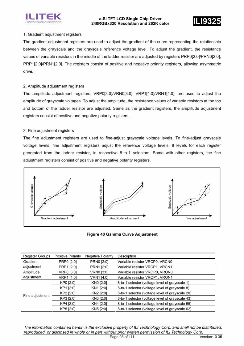
a-Si TFT LCD Single Chip Driver
240RGBx320 Resolution and 262K color ILI9325
The information contained herein is the exclusive property of ILI Technology Corp. and shall not be distributed, reproduced, or disclosed in whole or in part without prior written permission of ILI Technology Corp. Page 93 of 111 Version: 0.35
1. Gradient adjustment registers
The gradient adjustment registers are used to adjust the gradient of the curve representing the relationship
between the grayscale and the grayscale reference voltage level. To adjust the gradient, the resistance
values of variable resistors in the middle of the ladder resistor are adjusted by registers PRP0[2:0]/PRN0[2:0],
PRP1[2:0]/PRN1[2:0]. The registers consist of positive and negative polarity registers, allowing asymmetric
drive.
2. Amplitude adjustment registers
The amplitude adjustment registers, VRP0[3:0]/VRN0[3:0], VRP1[4:0]/VRN1[4:0], are used to adjust the
amplitude of grayscale voltages. To adjust the amplitude, the resistance values of variable resistors at the top
and bottom of the ladder resistor are adjusted. Same as the gradient registers, the amplitude adjustment
registers consist of positive and negative polarity registers.
3. Fine adjustment registers
The fine adjustment registers are used to fine-adjust grayscale voltage levels. To fine-adjust grayscale
voltage levels, fine adjustment registers adjust the reference voltage levels, 8 levels for each register
generated from the ladder resistor, in respective 8-to-1 selectors. Same with other registers, the fine
adjustment registers consist of positive and negative polarity registers.
Gradient adjustment
Gra
ysca
le v
olta
ge
Amplitude adjustment
Gra
ysca
le v
olta
ge
Fine adjustment
Gra
ysca
le v
olta
ge
Figure 40 Gamma Curve Adjustment
Register Groups Positive Polarity Negative Polarity Description PRP0 [2:0] PRN0 [2:0] Variable resistor VRCP0, VRCN0 Gradient
adjustment PRP1 [2:0] PRN1 [2:0] Variable resistor VRCP1, VRCN1 VRP0 [3:0] VRN0 [3:0] Variable resistor VROP0, VRON0 Amplitude
adjustment VRP1 [4:0] VRN1 [4:0] Variable resistor VROP1, VRON1 KP0 [2:0] KN0 [2:0] 8-to-1 selector (voltage level of grayscale 1) KP1 [2:0] KN1 [2:0] 8-to-1 selector (voltage level of grayscale 8) KP2 [2:0] KN2 [2:0] 8-to-1 selector (voltage level of grayscale 20) KP3 [2:0] KN3 [2:0] 8-to-1 selector (voltage level of grayscale 43) KP4 [2:0] KN4 [2:0] 8-to-1 selector (voltage level of grayscale 55)
Fine adjustment
KP5 [2:0] KN5 [2:0] 8-to-1 selector (voltage level of grayscale 62)
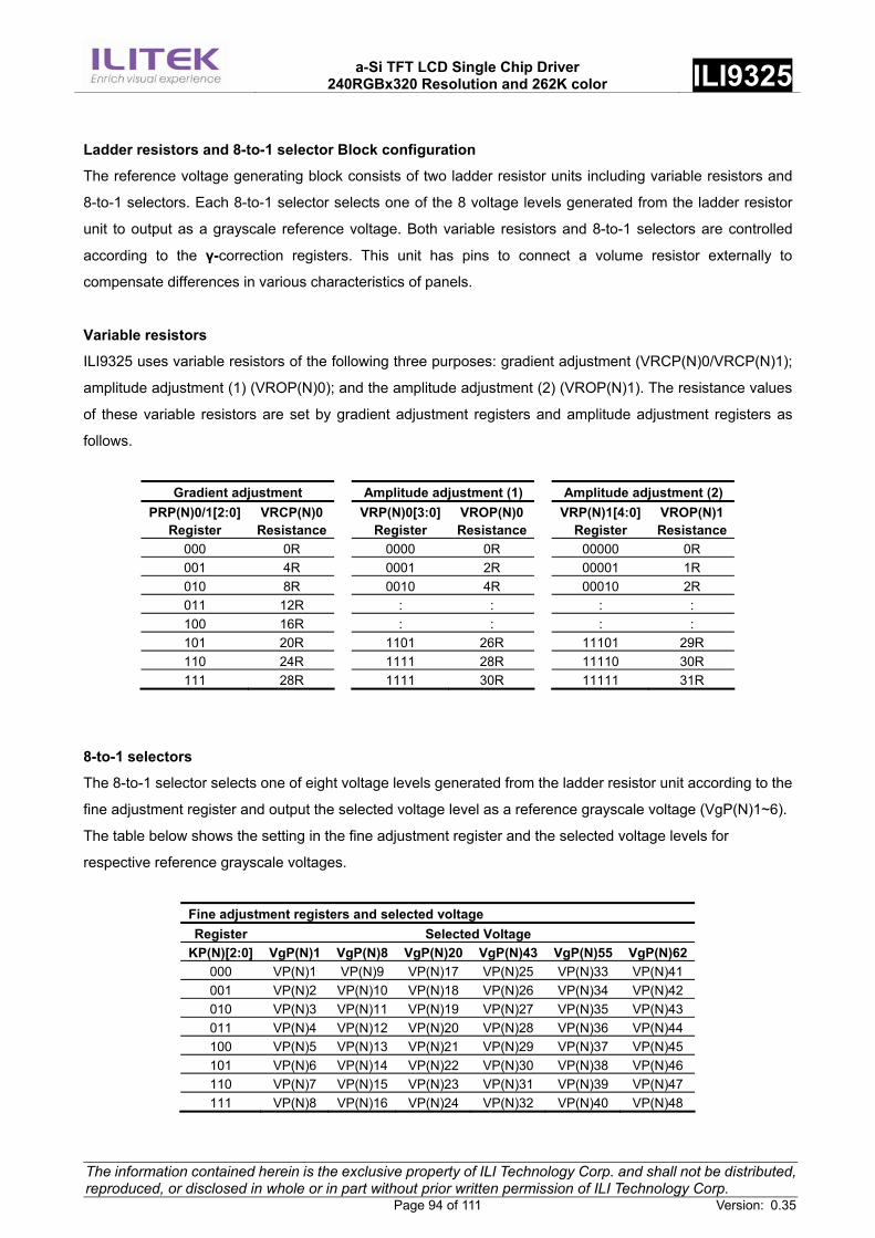
a-Si TFT LCD Single Chip Driver
240RGBx320 Resolution and 262K color ILI9325
The information contained herein is the exclusive property of ILI Technology Corp. and shall not be distributed, reproduced, or disclosed in whole or in part without prior written permission of ILI Technology Corp. Page 94 of 111 Version: 0.35
Ladder resistors and 8-to-1 selector Block configuration
The reference voltage generating block consists of two ladder resistor units including variable resistors and
8-to-1 selectors. Each 8-to-1 selector selects one of the 8 voltage levels generated from the ladder resistor
unit to output as a grayscale reference voltage. Both variable resistors and 8-to-1 selectors are controlled
according to the γ-correction registers. This unit has pins to connect a volume resistor externally to
compensate differences in various characteristics of panels.
Variable resistors
ILI9325 uses variable resistors of the following three purposes: gradient adjustment (VRCP(N)0/VRCP(N)1);
amplitude adjustment (1) (VROP(N)0); and the amplitude adjustment (2) (VROP(N)1). The resistance values
of these variable resistors are set by gradient adjustment registers and amplitude adjustment registers as
follows.
Gradient adjustment Amplitude adjustment (1) Amplitude adjustment (2) PRP(N)0/1[2:0]
Register VRCP(N)0
Resistance VRP(N)0[3:0]
Register VROP(N)0Resistance
VRP(N)1[4:0] Register
VROP(N)1Resistance
000 0R 0000 0R 00000 0R 001 4R 0001 2R 00001 1R 010 8R 0010 4R 00010 2R 011 12R : : : : 100 16R : : : : 101 20R 1101 26R 11101 29R 110 24R 1111 28R 11110 30R 111 28R 1111 30R 11111 31R
8-to-1 selectors
The 8-to-1 selector selects one of eight voltage levels generated from the ladder resistor unit according to the
fine adjustment register and output the selected voltage level as a reference grayscale voltage (VgP(N)1~6).
The table below shows the setting in the fine adjustment register and the selected voltage levels for
respective reference grayscale voltages.
Fine adjustment registers and selected voltage Register Selected Voltage
KP(N)[2:0] VgP(N)1 VgP(N)8 VgP(N)20 VgP(N)43 VgP(N)55 VgP(N)62 000 VP(N)1 VP(N)9 VP(N)17 VP(N)25 VP(N)33 VP(N)41 001 VP(N)2 VP(N)10 VP(N)18 VP(N)26 VP(N)34 VP(N)42 010 VP(N)3 VP(N)11 VP(N)19 VP(N)27 VP(N)35 VP(N)43 011 VP(N)4 VP(N)12 VP(N)20 VP(N)28 VP(N)36 VP(N)44 100 VP(N)5 VP(N)13 VP(N)21 VP(N)29 VP(N)37 VP(N)45 101 VP(N)6 VP(N)14 VP(N)22 VP(N)30 VP(N)38 VP(N)46 110 VP(N)7 VP(N)15 VP(N)23 VP(N)31 VP(N)39 VP(N)47 111 VP(N)8 VP(N)16 VP(N)24 VP(N)32 VP(N)40 VP(N)48
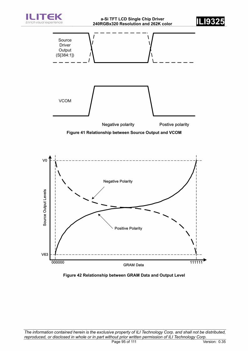
a-Si TFT LCD Single Chip Driver
240RGBx320 Resolution and 262K color ILI9325
The information contained herein is the exclusive property of ILI Technology Corp. and shall not be distributed, reproduced, or disclosed in whole or in part without prior written permission of ILI Technology Corp. Page 95 of 111 Version: 0.35
SourceDriverOutput
(S[384:1])
VCOM
Negative polarity Postive polarity Figure 41 Relationship between Source Output and VCOM
V0
V63
000000 111111GRAM Data
Sour
ce O
utpu
t Lev
els
Positive Polarity
Negative Polarity
Figure 42 Relationship between GRAM Data and Output Level
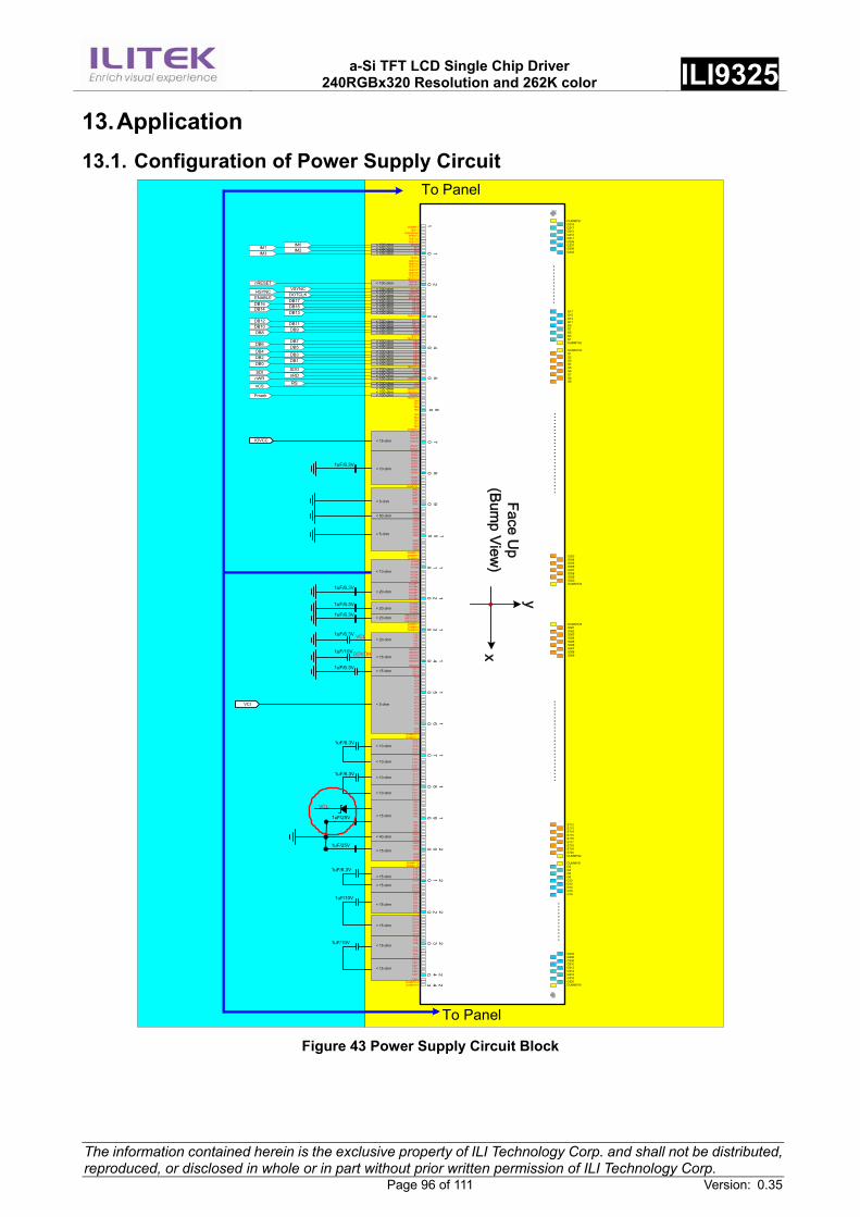
a-Si TFT LCD Single Chip Driver
240RGBx320 Resolution and 262K color ILI9325
The information contained herein is the exclusive property of ILI Technology Corp. and shall not be distributed, reproduced, or disclosed in whole or in part without prior written permission of ILI Technology Corp. Page 96 of 111 Version: 0.35
13. Application 13.1. Configuration of Power Supply Circuit
< 100 ohm< 100 ohm
< 100 ohm
Fmark
nCS RSnWR nRDSDI SDODB0 DB1DB2 DB3DB4
DB5DB6 DB7
DB8 DB9DB10 DB11DB12
DB13DB14 DB15DB16
DB17ENABLE
DOTCLKHSYNC VSYNCnRESET
IM3IM2IM1 IM0
< 15 ohm
< 15 ohm
< 15 ohm
< 15 ohm
< 15 ohm
< 15 ohm
< 15 ohm
< 5 ohm
< 20 ohm
< 10 ohm
< 5 ohm
< 5 ohm
< 100 ohm< 100 ohm< 100 ohm< 100 ohm< 100 ohm< 100 ohm< 100 ohm< 100 ohm< 100 ohm< 100 ohm
< 100 ohm< 100 ohm< 100 ohm< 100 ohm
< 100 ohm
< 100 ohm
< 100 ohm
1uF/10V
1uF/25V
1uF/25V
IOVCC
VCI X
Face Up
(Bump View
)
DUMMY23S361S362S363S364S365S366S367S368S369
x
y
S353S354S355S356S357S358S359S360DUMMY24
……
……
……
……
.
G304G306G308G310G312G314G316G318G320DUMMY20
DUMMY21G2G4G6G8G10G12G14G16G18
S712S713S714S715S716S717S718S719S720DUMMY22
……
……
DUMMY27G319G317G315G313G311G309G307G305G303
G17G15G13G11G9G7G5G3G1DUMMY26
DUMMY25S1S2S3S4S5S6S7S8S9
……
……
……
……
……
……
.
DUMMY1 TEST1
IOGNDDUMTESTO1 TESTO2 TESTO3
IM0/ID IM1 IM2 IM3
TEST2 TESTO4 TESTO5 TESTO6 TESTO7 TESTO8 TESTO9
TESTO10nRESET nRESET
VSYNC HSYNC
DOTCLK ENABLE
DB17 DB16 DB15 DB14 DB13
TESTO11
DB12 DB11 DB10
DB9 DB8
TEST3 TESTO12
DB7 DB6 DB5
DB4 DB3 DB2 DB1 DB0
TESTO13 SDO SDI
nRD nWR/SCL
RS nCS
TESTO14TESTO15
FMARK TESTO16
TS8 TS7 TS6 TS5
TS4 TS3 TS2 TS1 TS0
DUMMY2IOVCCIOVCCIOVCCIOVCC
IOVCC IOVCC VDDDVDDDVDDDVDDDVDDDVDDDVDDDVDDD
VDDDVDDDVDDD
DUMMY3GND GND GND GND GND GND
GNDGNDVGS VGS GNDGNDGNDGNDGNDGND
GND GND GND GND
DUMMY4DUMMY5DUMMY6
VCOM VCOM VCOM
VCOM VCOM VCOM VCOM
VCOMH VCOMH VCOMH VCOMH VCOMH VCOMH
VCOML VCOML VCOML VCOML
VREG1OUTVREG1OUTVREG1OUT
DUMMY7DUMMY8DUMMY9
VCL VCL VCL VCL VCL
DDVDH DDVDH DDVDH DDVDH DDVDH
DDVDHVCI1 VCI1 VCI1
VCI VCI VCI VCI VCI VCI
VCIVCIVCIVCIVCIVCIVCIVCIVCIVCI
VCI VCI
DUMMY10DUMMY11
C12-C12-C12-C12-C12-C12+C12+C12+C12+C12+C11-C11-C11-C11-C11-C11+C11+C11+C11+C11+VGL VGL VGL VGL VGL VGL
VGL VGL VGL VGL GNDGNDGNDVGH VGH VGH
VGH VGH VGH
DUMMY12DUMMY13
C13-C13-C13-C13-C13+
C22-C22-C22-C22-C22+C22+C22+C22+C22+C22+
C13+C13+C13+C21-C21-C21-C21-C21-C21-C21-
C21+C21+C21+C21+C21+C21+C21+C22-C22-C22-
C22+DUMMY14DUMMY15
110
2030
4050
6070
8090
100
110
120
130
140
150
160
170
180
190
200
210
220
230
240
243
< 100 ohm< 100 ohm< 100 ohm
1uF/10V
1uF/6.3V
< 40 ohm
1uF/6.3V
1uF/6.3V
1uF/6.3V
1uF/10V
1uF/6.3V
1uF/6.3V
1uF/6.3V
1uF/6.3V
1uF/6.3V
< 50 ohm
< 15 ohm
< 100 ohm< 100 ohm< 100 ohm
< 100 ohm< 100 ohm< 100 ohm< 100 ohm< 100 ohm< 100 ohm< 100 ohm< 100 ohm
< 100 ohm< 100 ohm< 100 ohm< 100 ohm< 100 ohm
< 10 ohm
< 20 ohm
< 20 ohm
< 20 ohm
< 15 ohm
< 15 ohm
< 10 ohm
< 10 ohm
< 10 ohm
< 10 ohm
< 15 ohm
To Panel
To Panel
VCL
VCL
DDVDH
Figure 43 Power Supply Circuit Block
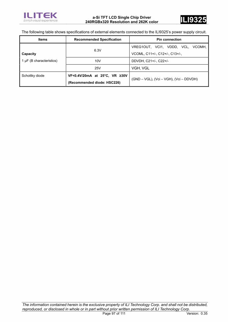
a-Si TFT LCD Single Chip Driver
240RGBx320 Resolution and 262K color ILI9325
The information contained herein is the exclusive property of ILI Technology Corp. and shall not be distributed, reproduced, or disclosed in whole or in part without prior written permission of ILI Technology Corp. Page 97 of 111 Version: 0.35
The following table shows specifications of external elements connected to the ILI9325’s power supply circuit.
Items Recommended Specification Pin connection
6.3V VREG1OUT, VCI1, VDDD, VCL, VCOMH,
VCOML, C11+/-, C12+/-, C13+/-,
10V DDVDH, C21+/-, C22+/-
Capacity
1 µF (B characteristics)
25V VGH, VGL
Schottky diode
VF<0.4V/20mA at 25°C, VR ≥30V
(Recommended diode: HSC226) (GND – VGL), (Vci – VGH), (Vci – DDVDH)
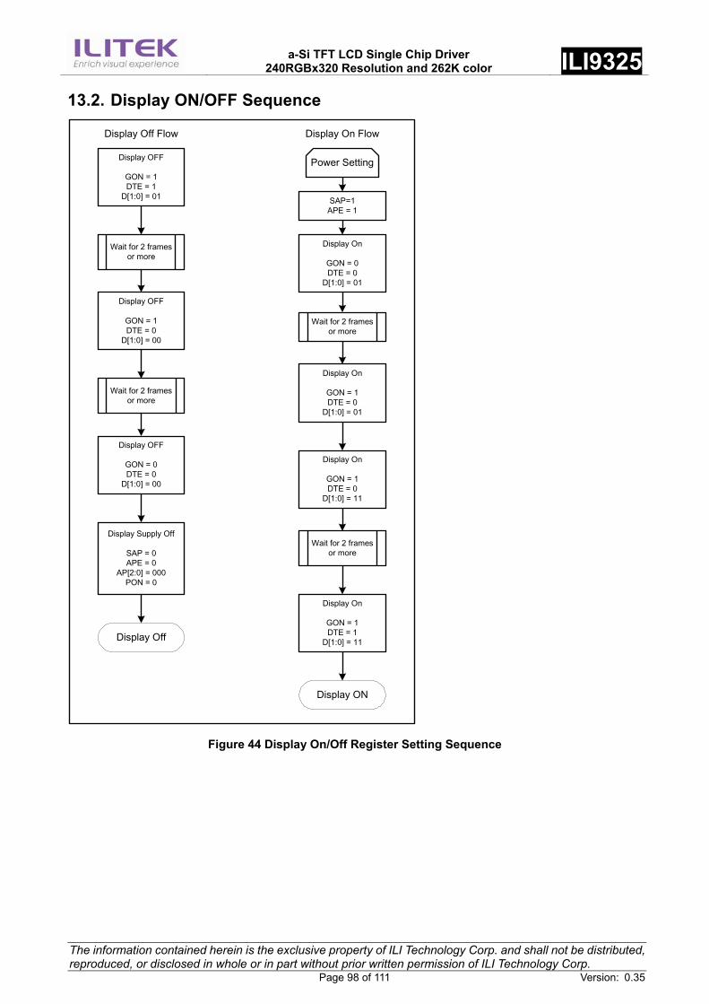
a-Si TFT LCD Single Chip Driver
240RGBx320 Resolution and 262K color ILI9325
The information contained herein is the exclusive property of ILI Technology Corp. and shall not be distributed, reproduced, or disclosed in whole or in part without prior written permission of ILI Technology Corp. Page 98 of 111 Version: 0.35
13.2. Display ON/OFF Sequence
Display OFF
GON = 1DTE = 1
D[1:0] = 01
Wait for 2 frames or more
Display OFF
GON = 1DTE = 0
D[1:0] = 00
Display Off Flow
Wait for 2 frames or more
Display OFF
GON = 0DTE = 0
D[1:0] = 00
Display Supply Off
SAP = 0APE = 0
AP[2:0] = 000PON = 0
Display Off
SAP=1APE = 1
Wait for 2 frames or more
Display On Flow
Display ON
Power Setting
Display On
GON = 0DTE = 0
D[1:0] = 01
Display On
GON = 1DTE = 0
D[1:0] = 01
Display On
GON = 1DTE = 0
D[1:0] = 11
Wait for 2 frames or more
Display On
GON = 1DTE = 1
D[1:0] = 11
Figure 44 Display On/Off Register Setting Sequence
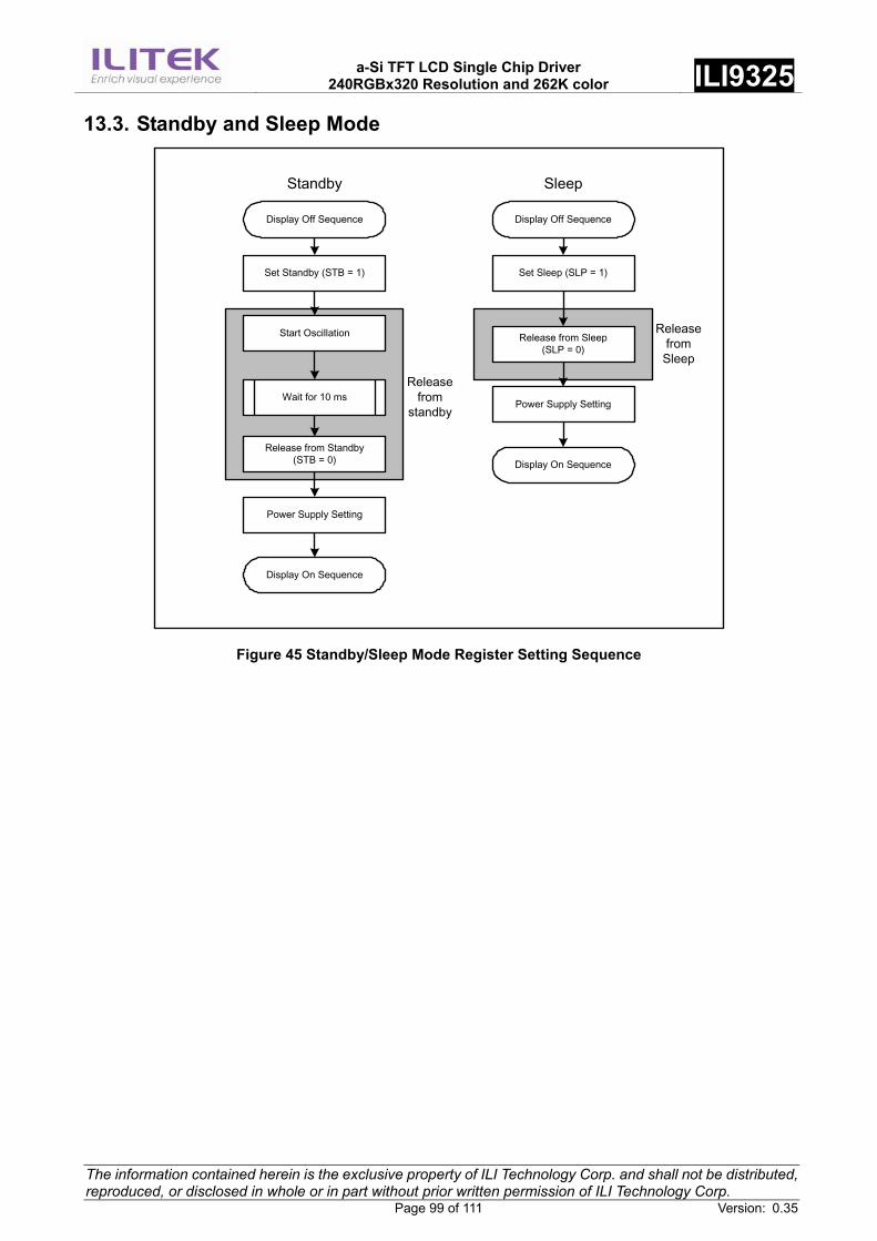
a-Si TFT LCD Single Chip Driver
240RGBx320 Resolution and 262K color ILI9325
The information contained herein is the exclusive property of ILI Technology Corp. and shall not be distributed, reproduced, or disclosed in whole or in part without prior written permission of ILI Technology Corp. Page 99 of 111 Version: 0.35
13.3. Standby and Sleep Mode
Set Standby (STB = 1)
Display Off Sequence
Start Oscillation
Wait for 10 ms
Release from Standby(STB = 0)
Power Supply Setting
Display On Sequence
Standby
Set Sleep (SLP = 1)
Display Off Sequence
Release from Sleep(SLP = 0)
Power Supply Setting
Display On Sequence
Sleep
Release from
standby
Release from Sleep
Figure 45 Standby/Sleep Mode Register Setting Sequence
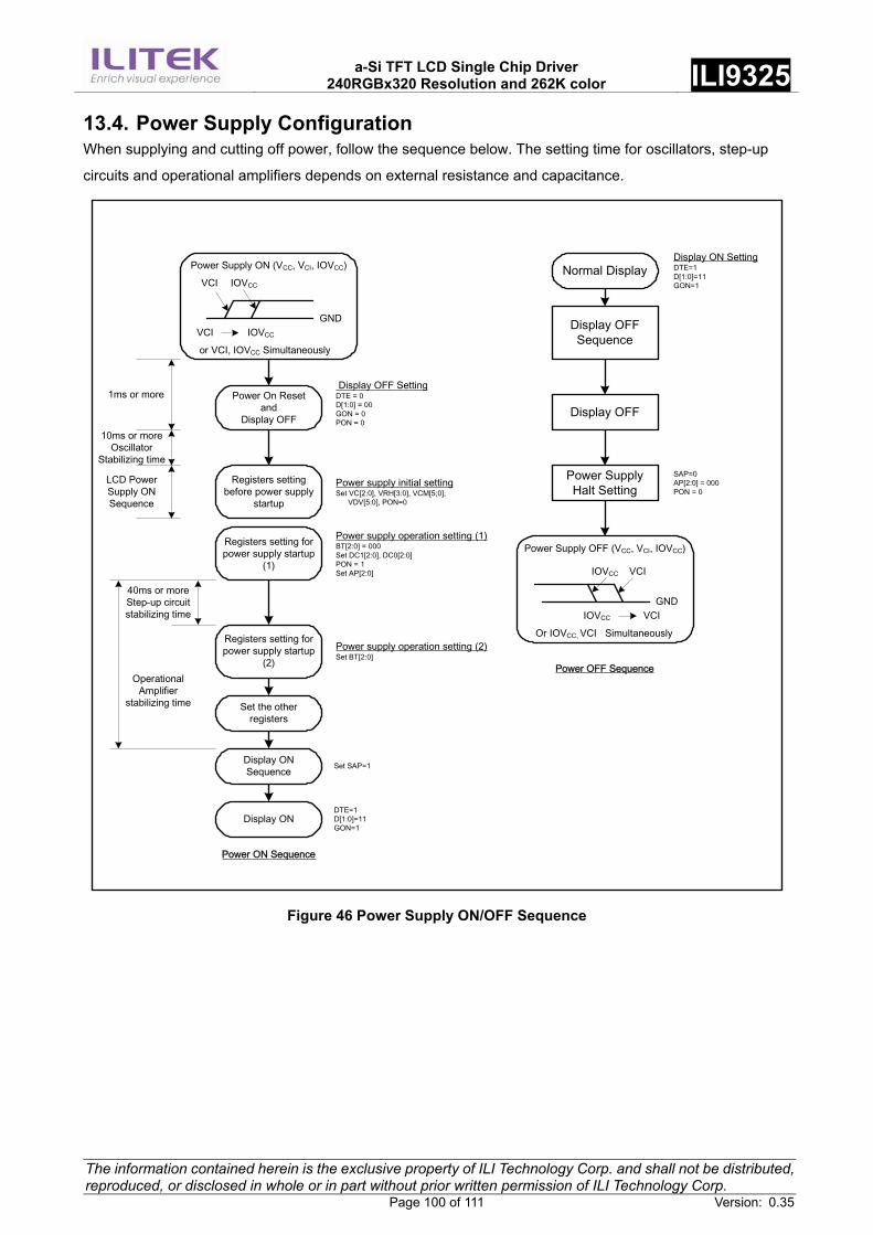
a-Si TFT LCD Single Chip Driver
240RGBx320 Resolution and 262K color ILI9325
The information contained herein is the exclusive property of ILI Technology Corp. and shall not be distributed, reproduced, or disclosed in whole or in part without prior written permission of ILI Technology Corp. Page 100 of 111 Version: 0.35
13.4. Power Supply Configuration When supplying and cutting off power, follow the sequence below. The setting time for oscillators, step-up
circuits and operational amplifiers depends on external resistance and capacitance.
Power Supply ON (VCC, VCI, IOVCC)VCI IOVCC
GNDVCI IOVCC
or VCI, IOVCC Simultaneously
Power On Reset and
Display OFF
Registers setting before power supply
startup
Display OFF Setting DTE = 0 D[1:0] = 00GON = 0PON = 0
1ms or more
10ms or moreOscillator
Stabilizing time
LCD Power Supply ON Sequence
Power supply initial setting Set VC[2:0], VRH[3:0], VCM[5;0], VDV[5:0], PON=0
Registers setting for power supply startup
(1)
Power supply operation setting (1) BT[2:0] = 000Set DC1[2:0], DC0[2:0]PON = 1Set AP[2:0]
Registers setting for power supply startup
(2)
40ms or more Step-up circuit stabilizing time
Power supply operation setting (2) Set BT[2:0]
Set the other registers
Display ONSequence
Display ON
Operational Amplifier
stabilizing time
Set SAP=1
DTE=1D[1:0]=11GON=1
Power ON Sequence
Normal Display
Display OFFSequence
Display OFF
Power Supply Halt Setting
Display ON Setting DTE=1D[1:0]=11GON=1
SAP=0AP[2:0] = 000PON = 0
Power Supply OFF (VCC, VCI, IOVCC)
VCIIOVCC
GNDIOVCC VCI
Or IOVCC, VCI Simultaneously
Power OFF Sequence
Figure 46 Power Supply ON/OFF Sequence
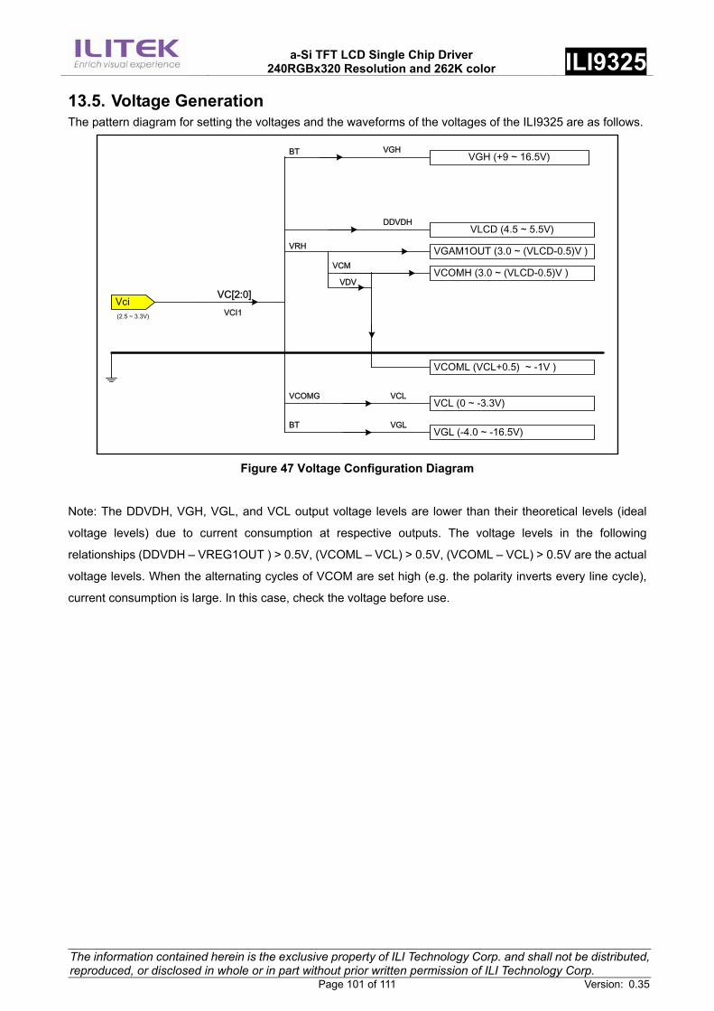
a-Si TFT LCD Single Chip Driver
240RGBx320 Resolution and 262K color ILI9325
The information contained herein is the exclusive property of ILI Technology Corp. and shall not be distributed, reproduced, or disclosed in whole or in part without prior written permission of ILI Technology Corp. Page 101 of 111 Version: 0.35
13.5. Voltage Generation The pattern diagram for setting the voltages and the waveforms of the voltages of the ILI9325 are as follows.
Vci(2.5 ~ 3.3V)
VGH (+9 ~ 16.5V)
VLCD (4.5 ~ 5.5V)
VGAM1OUT (3.0 ~ (VLCD-0.5)V )
VCOMH (3.0 ~ (VLCD-0.5)V )
VCOML (VCL+0.5) ~ -1V )
BT
VRH
VCL (0 ~ -3.3V)VCOMG
VGL (-4.0 ~ -16.5V)BT
VCI1
VC[2:0]VDV
VGL
VCL
VGH
DDVDH
VCM
Figure 47 Voltage Configuration Diagram
Note: The DDVDH, VGH, VGL, and VCL output voltage levels are lower than their theoretical levels (ideal
voltage levels) due to current consumption at respective outputs. The voltage levels in the following
relationships (DDVDH – VREG1OUT ) > 0.5V, (VCOML – VCL) > 0.5V, (VCOML – VCL) > 0.5V are the actual
voltage levels. When the alternating cycles of VCOM are set high (e.g. the polarity inverts every line cycle),
current consumption is large. In this case, check the voltage before use.
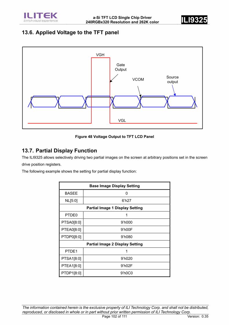
a-Si TFT LCD Single Chip Driver
240RGBx320 Resolution and 262K color ILI9325
The information contained herein is the exclusive property of ILI Technology Corp. and shall not be distributed, reproduced, or disclosed in whole or in part without prior written permission of ILI Technology Corp. Page 102 of 111 Version: 0.35
13.6. Applied Voltage to the TFT panel
SourceoutputVCOM
GateOutput
VGH
VGL
Figure 48 Voltage Output to TFT LCD Panel
13.7. Partial Display Function The ILI9325 allows selectively driving two partial images on the screen at arbitrary positions set in the screen
drive position registers.
The following example shows the setting for partial display function:
Base Image Display Setting
BASEE 0
NL[5:0] 6’h27
Partial Image 1 Display Setting
PTDE0 1
PTSA0[8:0] 9’h000
PTEA0[8:0] 9’h00F
PTDP0[8:0] 9’h080
Partial Image 2 Display Setting
PTDE1 1
PTSA1[8:0] 9’h020
PTEA1[8:0] 9’h02F
PTDP1[8:0] 9’h0C0
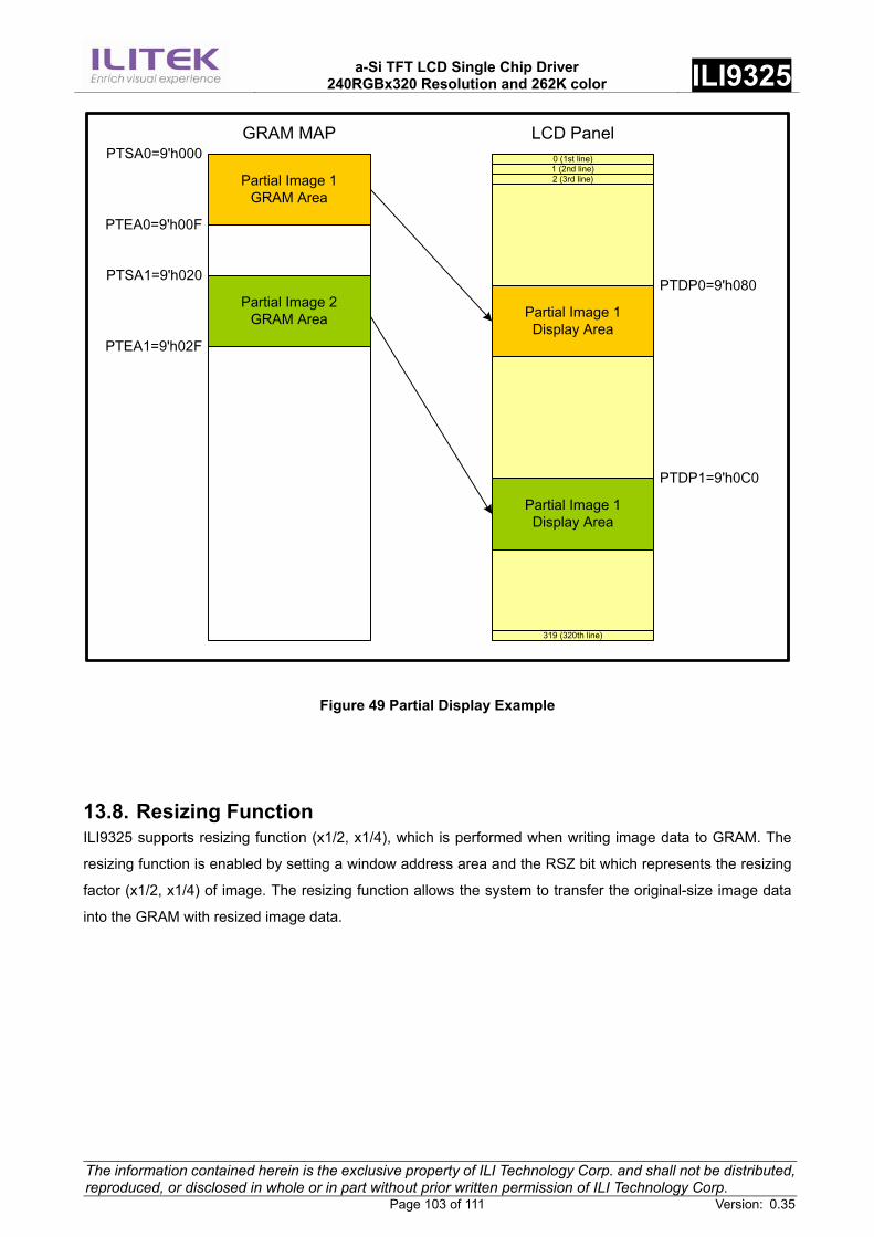
a-Si TFT LCD Single Chip Driver
240RGBx320 Resolution and 262K color ILI9325
The information contained herein is the exclusive property of ILI Technology Corp. and shall not be distributed, reproduced, or disclosed in whole or in part without prior written permission of ILI Technology Corp. Page 103 of 111 Version: 0.35
0 (1st line)1 (2nd line)2 (3rd line)
Partial Image 1Display Area
Partial Image 1GRAM Area
Partial Image 2GRAM Area
Partial Image 1Display Area
319 (320th line)
GRAM MAP LCD PanelPTSA0=9'h000
PTEA0=9'h00F
PTSA1=9'h020
PTEA1=9'h02F
PTDP0=9'h080
PTDP1=9'h0C0
Figure 49 Partial Display Example
13.8. Resizing Function ILI9325 supports resizing function (x1/2, x1/4), which is performed when writing image data to GRAM. The
resizing function is enabled by setting a window address area and the RSZ bit which represents the resizing
factor (x1/2, x1/4) of image. The resizing function allows the system to transfer the original-size image data
into the GRAM with resized image data.
a-Si TFT LCD Single Chip Driver
240RGBx320 Resolution and 262K color ILI9325
The information contained herein is the exclusive property of ILI Technology Corp. and shall not be distributed, reproduced, or disclosed in whole or in part without prior written permission of ILI Technology Corp. Page 104 of 111 Version: 0.35
(0,0)
(1,0)
(2,0)
(3,0)
(4,0)
(5,0)
(0,1)
(1,1)
(2,1)
(3,1)
(4,1)
(5,1)
(0,2)
(1,2)
(2,2)
(3,2)
(4,2)
(5,2)
(0,3)
(1,3)
(2,3)
(3,3)
(4,3)
(5,3)
(0,4)
(1,4)
(2,4)
(3,4)
(4,4)
(5,4)
(0,5)
(1,5)
(2,5)
(3,5)
(4,5)
(5,5)
(6,0) (6,1) (6,2) (6,3) (6,4) (6,5)
(0,6)
(1,6)
(2,6)
(3,6)
(4,6)
(5,6)
(6,6)
0 1 2 3 4 5 60123456
(0,0)
(2,0)
(4,0)
(0,2)
(2,2)
(4,2)
(0,4)
(2,4)
(4,4)
(6,0) (6,2) (6,4)
(0,6)
(2,6)
(4,6)
(6,6)
? resizing
Original Image Data GRAM Data
Figure 50 Data transfer in resizing
Write to GRAM
RSZ=2'h1
Original Data240
320
Panel Display
120
160
Figure 51 Resizing Example
Resized Image Resolution Original Image Size (X × Y)1/2 (RSZ=2’h1) 1/4 (RSZ=2’h3)
640 × 480 320 × 240 160 × 120 352 × 288 176 × 144 88 × 72 320 × 240 160 × 120 80× 60 176 × 144 88 × 72 44× 36 120 × 160 60× 80 30 × 40 132 × 132 66 × 66 33 × 33
The RSZ bit sets the resizing factor of an image. When setting a window address area in the internal GRAM,
the GRAM window address area must fit the size of resized image. The following example show the resizing
setting.
a-Si TFT LCD Single Chip Driver
240RGBx320 Resolution and 262K color ILI9325
The information contained herein is the exclusive property of ILI Technology Corp. and shall not be distributed, reproduced, or disclosed in whole or in part without prior written permission of ILI Technology Corp. Page 105 of 111 Version: 0.35
X
Y Original ImageSize
(X0, Y0)
(X0+dx-1, Y0+dy-1)
dx
dy
dx= (X-H)/N, H=X mod Ndy= (Y-V)/N, V=Y mod N
GRAM Address
Original image data number in horizontal direction X
Original image data number in Vertical direction Y
Resizing Ration 1/N
Resizing Setting RSZ N-1
Remainder pixels in horizontal direction RCH H
Remainder pixels in vertical direction RCV V
GRAM writing start address AD (x0, y0)
HSA x0
HEA x0+dx-1
VSA y0 GRAM window setting
VEA y0+dy-1
a-Si TFT LCD Single Chip Driver
240RGBx320 Resolution and 262K color ILI9325
The information contained herein is the exclusive property of ILI Technology Corp. and shall not be distributed, reproduced, or disclosed in whole or in part without prior written permission of ILI Technology Corp. Page 106 of 111 Version: 0.35
14. Electrical Characteristics
14.1. Absolute Maximum Ratings The absolute maximum rating is listed on following table. When ILI9325 is used out of the absolute maximum
ratings, the ILI9325 may be permanently damaged. To use the ILI9325 within the following electrical
characteristics limit is strongly recommended for normal operation. If these electrical characteristic conditions
are exceeded during normal operation, the ILI9325 will malfunction and cause poor reliability.
Item Symbol Unit Value Note Power supply voltage (1) IOVCC V -0.3 ~ + 4.6 1, 2 Power supply voltage (1) VCI - GND V -0.3 ~ + 4.6 1, 4 Power supply voltage (1) DDVDH - GND V -0.3 ~ + 6.0 1, 4 Power supply voltage (1) GND -VCL V -0.3 ~ + 4.6 1 Power supply voltage (1) DDVDH - VCL V -0.3 ~ + 9.0 1, 5 Power supply voltage (1) VGH - GND V -0.3 ~ + 18.5 1, 5 Power supply voltage (1) GND - VGL V -0.3 ~ + 18.5 1, 6 Input voltage Vt V -0.3 ~ VCC+ 0.3 1 Operating temperature Topr °C -40 ~ + 85 8, 9 Storage temperature Tstg °C -55 ~ + 110 8, 9 Notes: 1. GND must be maintained 2. (High) (VCC = VCC) ≥ GND (Low), (High) IOVCC ≥ GND (Low). 3. Make sure (High) VCI ≥ GND (Low). 4. Make sure (High) DDVDH ≥ GND (Low). 5. Make sure (High) DDVDH ≥ VCL (Low). 6. Make sure (High) VGH ≥ GND (Low). 7. Make sure (High) GND ≥ VGL (Low). 8. For die and wafer products, specified up to 85°C. 9. This temperature specifications apply to the TCP package
a-Si TFT LCD Single Chip Driver
240RGBx320 Resolution and 262K color ILI9325
The information contained herein is the exclusive property of ILI Technology Corp. and shall not be distributed, reproduced, or disclosed in whole or in part without prior written permission of ILI Technology Corp. Page 107 of 111 Version: 0.35
14.2. DC Characteristics (VCC = VCI=2.40 ~ 3.0V, IOVCC = 1.65 ~ 3.30V, Ta= -40 ~ 85 °C)
Item Symbol Unit Test Condition Min. Typ. Max. NoteInput high voltage VIH V IOVCC= 1.8 ~ 3.3V 0.8*IOVCC - IOVCC - Input low voltage VIL V IOVCC= 1.8 ~ 3.3V -0.3 - 0.2*IOVCC - Output high voltage(1) ( DB0-17 Pins)
VOH1 V IOH = -0.1 mA 0.8*IOVCC - - -
Output low voltage ( DB0-17 Pins)
VOL1 V IOVCC=1.65~3.3V - - 0.2*IOVCC -
I/O leakage current ILI µA Vin = 0 ~ VCC -0.1 - 0.1 - Current consumption during normal operation (VCC – GND )
IOP µA VCC=2.8V , Ta=25°C , fOSC = 512KHz ( Line) GRAM data = 0000h
- 100
(VCC) - -
Current consumption during standby mode (VCC – GND )
IST µA VCI=2.8V , Ta=25 °C - 30 50 -
LCD Drive Power Supply Current ( DDVDH-GND )
ILCD mA
VCI=2.8V , VREG1OUT =4.8V DDVDH=5.2V , Frame Rate: 70Hz, line-inversion, Ta=25 °C, GRAM data = 0000h,
- 5.0 - -
LCD Driving Voltage ( DDVDH-GND )
DDVDH V - 4.5 - 6 -
Dispersion of the Average Output Voltage
V mV - -10 - 10 -
14.3. Reset Timing Characteristics Reset Timing Characteristics (IOVCC = 1.65 ~ 3.3 V) Item Symbol Unit Min. Typ. Max. Reset low-level width tRES ms 1 - - Reset rise time trRES µs - - 10
VIL
VIHnRESET
tREStrRES
14.4. AC Characteristics
14.4.1. i80-System Interface Timing Characteristics
Normal Write Mode (IOVCC = 1.65~3.3V) Item Symbol Unit Min. Typ. Max. Test Condition
Write tCYCW ns 100 - - - Bus cycle time Read tCYCR ns 300 - - -
Write low-level pulse width PWLW ns 50 - 500 - Write high-level pulse width PWHW ns 50 - - - Read low-level pulse width PWLR ns 150 - - - Read high-level pulse width PWHR ns 150 - -
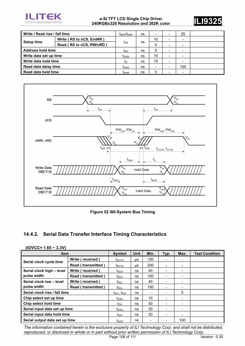
a-Si TFT LCD Single Chip Driver
240RGBx320 Resolution and 262K color ILI9325
The information contained herein is the exclusive property of ILI Technology Corp. and shall not be distributed, reproduced, or disclosed in whole or in part without prior written permission of ILI Technology Corp. Page 108 of 111 Version: 0.35
Write / Read rise / fall time tWRr/tWRf ns - - 25 Write ( RS to nCS, E/nWR ) 10 - - Setup time Read ( RS to nCS, RW/nRD )
tAS ns 5 - -
Address hold time tAH ns 5 - - Write data set up time tDSW ns 10 - - Write data hold time tH ns 15 - - Read data delay time tDDR ns - - 100 Read data hold time tDHR ns 5 - -
VIHVIL
VIHVIL
VIL
tAS
tWRf
VIL
VIH
tAH
tWRr
VIH
tCYCW, tCYCR
VIH
VIL
VIHVIL
VIH
VOHVOL
VOHVOL
tDDR tDHR
tDSW tH
PWLW, PWLR PWHW, PWHR
RS
nCS
nWR, nRD
Write DataDB[17:0]
Read DataDB[17:0]
Valid Data
Valid Data
Figure 52 i80-System Bus Timing
14.4.2. Serial Data Transfer Interface Timing Characteristics (IOVCC= 1.65 ~ 3.3V)
Item Symbol Unit Min. Typ. Max. Test ConditionWrite ( received ) tSCYC µs 100 - - Serial clock cycle time Read ( transmitted ) tSCYC µs 200 - - Write ( received ) tSCH ns 40 - - Serial clock high – level
pulse width Read ( transmitted ) tSCH ns 100 - - Write ( received ) tSCL ns 40 - - Serial clock low – level
pulse width Read ( transmitted ) tSCL ns 100 - - Serial clock rise / fall time tSCr, tSCf ns - - 5 Chip select set up time tCSU ns 10 - - Chip select hold time tCH ns 50 - - Serial input data set up time tSISU ns 20 - - Serial input data hold time tSIH ns 20 - - Serial output data set up time tSOD ns - - 100
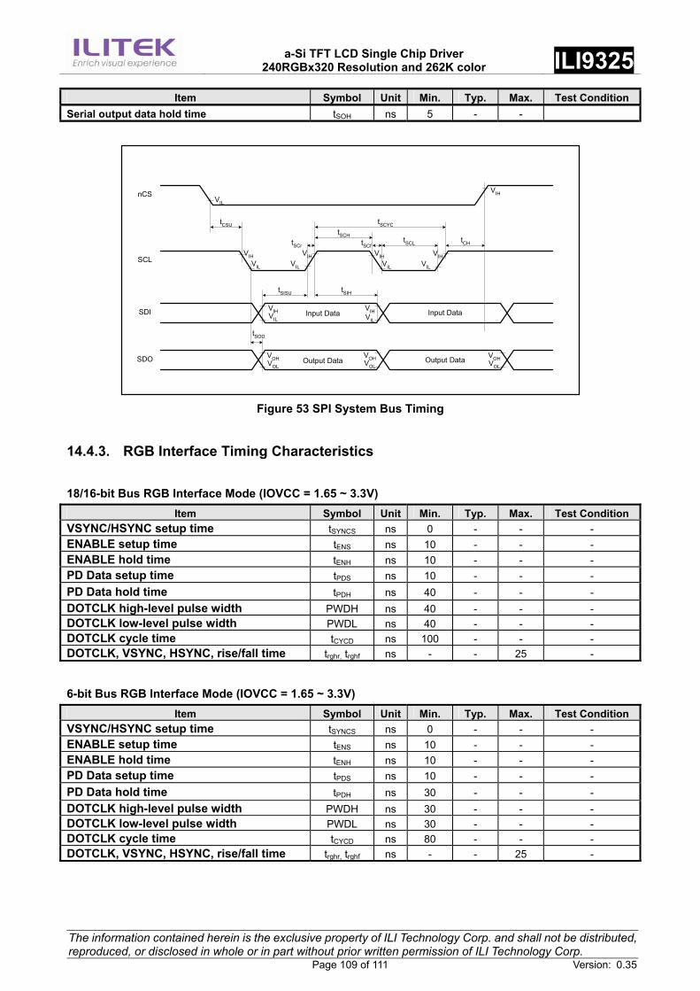
a-Si TFT LCD Single Chip Driver
240RGBx320 Resolution and 262K color ILI9325
The information contained herein is the exclusive property of ILI Technology Corp. and shall not be distributed, reproduced, or disclosed in whole or in part without prior written permission of ILI Technology Corp. Page 109 of 111 Version: 0.35
Item Symbol Unit Min. Typ. Max. Test ConditionSerial output data hold time tSOH ns 5 - -
VIL
tCSU
VIHVIL
VIHVIL
VIHVIL
VIHVIL
tSISU
VIHVIL
VIHVIL
tSIH
tSCr tSCf
tSCHtSCL
tSCYC
tCH
VIH
Input Data Input Data
VOHVOL
Output Data Output Data
tSOD
VOHVOL
VOHVOL
nCS
SCL
SDI
SDO
Figure 53 SPI System Bus Timing
14.4.3. RGB Interface Timing Characteristics
18/16-bit Bus RGB Interface Mode (IOVCC = 1.65 ~ 3.3V) Item Symbol Unit Min. Typ. Max. Test Condition
VSYNC/HSYNC setup time tSYNCS ns 0 - - - ENABLE setup time tENS ns 10 - - - ENABLE hold time tENH ns 10 - - - PD Data setup time tPDS ns 10 - - - PD Data hold time tPDH ns 40 - - - DOTCLK high-level pulse width PWDH ns 40 - - - DOTCLK low-level pulse width PWDL ns 40 - - - DOTCLK cycle time tCYCD ns 100 - - - DOTCLK, VSYNC, HSYNC, rise/fall time trghr, trghf ns - - 25 -
6-bit Bus RGB Interface Mode (IOVCC = 1.65 ~ 3.3V) Item Symbol Unit Min. Typ. Max. Test Condition
VSYNC/HSYNC setup time tSYNCS ns 0 - - - ENABLE setup time tENS ns 10 - - - ENABLE hold time tENH ns 10 - - - PD Data setup time tPDS ns 10 - - - PD Data hold time tPDH ns 30 - - - DOTCLK high-level pulse width PWDH ns 30 - - - DOTCLK low-level pulse width PWDL ns 30 - - - DOTCLK cycle time tCYCD ns 80 - - - DOTCLK, VSYNC, HSYNC, rise/fall time trghr, trghf ns - - 25 -
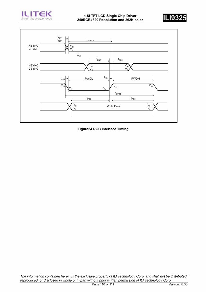
a-Si TFT LCD Single Chip Driver
240RGBx320 Resolution and 262K color ILI9325
The information contained herein is the exclusive property of ILI Technology Corp. and shall not be distributed, reproduced, or disclosed in whole or in part without prior written permission of ILI Technology Corp. Page 110 of 111 Version: 0.35
VIHVIL
tASE
HSYNCVSYNC
VIHVIL
VIHVIL
HSYNCVSYNC
VIHVIL
VIHVIL
trgbftrgbr
VIH
tSYNCS
VILVIL
VIH
tENS
PWDLtrgbftrgbr PWDH
tENH
tPDS tPDH
tCYCD
VIH
Write Data
Figure54 RGB Interface Timing
a-Si TFT LCD Single Chip Driver
240RGBx320 Resolution and 262K color ILI9325
The information contained herein is the exclusive property of ILI Technology Corp. and shall not be distributed, reproduced, or disclosed in whole or in part without prior written permission of ILI Technology Corp. Page 111 of 111 Version: 0.35
15. Revision History Version No. Date Page Description
V0.28 2007/07/05 96 Modify the FPC circuit
V0.29 2007/07/12 15 Modify the alignment mark pattern
V0.30 2007/09/07 55 Modify the frame rate setting of R2Bh register
V0.31 2007/10/29 57 Add the high speed write function
V0.32 2007/11/02 71、72 Modify Frame rate value by register setting
V0.33 2007/11/08 105 Delete Output Voltage deviation item
V0.34 2007/11/27 96 Modify the pin recommend resistance
V0.35 2007/11/30 96 Remove the TEST1 and TEST2 output to FPC.