Embed Size (px)
Citation preview

This article has been accepted for inclusion in a future issue of this journal. Content is final as presented, with the exception of pagination.
IEEE TRANSACTIONS ON VERY LARGE SCALE INTEGRATION (VLSI) SYSTEMS 1
A Single-Ended With Dynamic Feedback Control8T Subthreshold SRAM Cell
C. B. Kushwah, Student Member, IEEE and S. K. Vishvakarma, Member, IEEE
Abstract— A novel 8-transistor (8T) static random access memorycell with improved data stability in subthreshold operation is designed.The proposed single-ended with dynamic feedback control 8T staticRAM (SRAM) cell enhances the static noise margin (SNM) for ultralowpower supply. It achieves write SNM of 1.4× and 1.28× as that ofisoarea 6T and read-decoupled 8T (RD-8T), respectively, at 300 mV. Thestandard deviation of write SNM for 8T cell is reduced to 0.4× and 0.56×as that for 6T and RD-8T, respectively. It also possesses another strikingfeature of high read SNM ∼2.33×, 1.23×, and 0.89× as that of 5T, 6T,and RD-8T, respectively. The cell has hold SNM of 1.43×, 1.23×, and1.05× as that of 5T, 6T, and RD-8T, respectively. The write time is 71%lesser than that of single-ended asymmetrical 8T cell. The proposed 8Tconsumes less write power 0.72×, 0.6×, and 0.85× as that of 5T, 6T, andisoarea RD-8T, respectively. The read power is 0.49× of 5T, 0.48× of 6T,and 0.64× of RD-8T. The power/energy consumption of 1-kb 8T SRAMarray during read and write operations is 0.43× and 0.34×, respectively,of 1-kb 6T array. These features enable ultralow power applications of 8T.
Index Terms— Single ended, static noise margin (SNM), staticRAM (SRAM), subthreshold, ultralow power.
I. INTRODUCTION
The portable microprocessor controlled devices contain embed-ded memory, which represents a large portion of the system-on-chip (SoC). These portable systems need ultralow power consumingcircuits to utilize battery for longer duration. The power consump-tion can be minimized using nonconventional device structures,new circuit topologies, and optimizing the architecture. Although,voltage scaling has led to circuit operation in subthreshold regimewith minimum power consumption, but there is a disadvantage ofexponential reduction in performance [1]. The circuit operation in thesubthreshold regime has paved path toward ultralow power embeddedmemories, mainly static RAMs (SRAMs) [1], [2]. However, insubthreshold regime, the data stability of SRAM cell is a severeproblem and worsens with the scaling of MOSFET to subnanometertechnology. Due to these limitations it becomes difficult to operatethe conventional 6-transistor (6T) cell at ultralow voltage (ULV)power supply [1]–[6]. In addition, 6T has a severe problem of readdisturb. The basic and an effective way to eliminate this problemis the decoupling of true storing node from the bit lines duringthe read operation in [2]. This read decoupling approach is utilizedby conventional 8-transistor [read decoupled 8-transistor (RD-8T)]cell which offers read static noise margin (RSNM) comparablewith hold static noise margin (HSNM) [2]–[4]. However, RD-8Tsuffers from leakage introduced in read path. This leakage currentincreases with the scaling thereby, increasing the probability of failedread/write operations. Similar cells that maintain the cell currentwithout disturbing the storage node are also proposed in [4]–[7].
Manuscript received July 28, 2014; revised October 28, 2014,December 6, 2014, and January 5, 2015; accepted January 5, 2015.
The authors are with the Nanoscale Devices and VLSI/ULSICircuit and System Design Laboratory, Discipline of Electrical Engineering,IIT Indore, Indore 452017, India (e-mail: [email protected];[email protected]).
Color versions of one or more of the figures in this paper are availableonline at http://ieeexplore.ieee.org.
Digital Object Identifier 10.1109/TVLSI.2015.2389891
Fig. 1. Proposed 8T. (a) Schematic. (b) Layout.
Furthermore, to reduce the power consumption of differential bit line,a single-ended 5T bit cell is attractive due to its reduced area andconsiderable active and standby power saving capability as comparedwith conventional 6T SRAM cell [8]. However, writing 1 through annMOS pass transistor in 5T is a design challenge. Another problemis to obtain optimized noise margin against process variations at alloperations. In addition, the read stability of single ended 5T severelydegrades in comparison with conventional 6T SRAM cell [8]. Variousapproaches like boosted supply (gate voltage of access transistorM5 is greater than VDD) generated from an additional circuit [8],gated-feedback write assist [9], 7T dual VTH [10], asymmetricalwrite/read-assist 8T [11], and cross-point data-aware 9T [12] havebeen proposed to mitigate the above issues associated with 5T. Still,none of the cell could fulfill the requirement of improving bothread and write stability in subthreshold regime for ultralow powerapplications.
In this brief, we have designed a new subthreshold 8T SRAMcell that operates in subnanometer technology node at ULV. This8T SRAM cell uses single-ended write with dynamic feedback cuttingto enhance writeability and dynamic read decoupling to avoid readdisturb [12]–[16]. Due to read decoupled mechanism, the 9T cell [16]improves the RSNM by 4.1× as compared with conventional 6Tcell. The 9T cell not only has larger write margin (WT) but also hasfaster write time [16]. As 8T is single-ended it can save more powerconsumption and area as compared with [16]. Here, we focus mainlyon the stability of the cell which is affected by the process parametervariations. This brief is an elaborate discussion of our previouswork [15] on 8T, including comparisons with other single-endedcells like conventional 5T and 8T [11]. We have also emphasized ondelay, power and half-select issues for both row and column. Apartfrom this, a 1-kb SRAM array for proposed 8T and conventional6T was also designed. The circuit simulations are done in UnitedMicroelectronics Corporation (UMC) 90-nm process technology atdifferent power supplies.
II. PROPOSED 8T SRAM CELL DESIGN
To make a cell stable in all operations, single-ended with dynamicfeedback control (SE-DFC) cell is presented in Fig. 1(a). Thesingle-ended design is used to reduce the differential switching powerduring read–write operation. The power consumed during switching/toggling of data on single bit line is lesser than that on differential
1063-8210 © 2015 IEEE. Personal use is permitted, but republication/redistribution requires IEEE permission.See http://www.ieee.org/publications_standards/publications/rights/index.html for more information.
This article has been accepted for inclusion in a future issue of this journal. Content is final as presented, with the exception of pagination.
2 IEEE TRANSACTIONS ON VERY LARGE SCALE INTEGRATION (VLSI) SYSTEMS
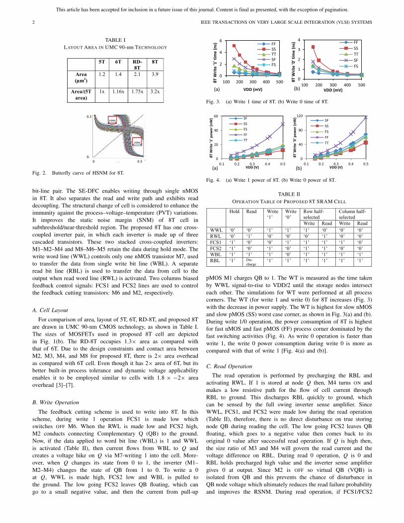
TABLE ILAYOUT AREA IN UMC 90-nm TECHNOLOGY
Fig. 2. Butterfly curve of HSNM for 8T.
bit-line pair. The SE-DFC enables writing through single nMOSin 8T. It also separates the read and write path and exhibits readdecoupling. The structural change of cell is considered to enhance theimmunity against the process–voltage–temperature (PVT) variations.It improves the static noise margin (SNM) of 8T cell insubthreshold/near-threshold region. The proposed 8T has one cross-coupled inverter pair, in which each inverter is made up of threecascaded transistors. These two stacked cross-coupled inverters:M1–M2–M4 and M8–M6–M5 retain the data during hold mode. Thewrite word line (WWL) controls only one nMOS transistor M7, usedto transfer the data from single write bit line (WBL). A separateread bit line (RBL) is used to transfer the data from cell to theoutput when read word line (RWL) is activated. Two columns biasedfeedback control signals: FCS1 and FCS2 lines are used to controlthe feedback cutting transistors: M6 and M2, respectively.
A. Cell Layout
For comparison of area, layout of 5T, 6T, RD-8T, and proposed 8Tare drawn in UMC 90-nm CMOS technology, as shown in Table I.The sizes of MOSFETs used in proposed 8T cell are depictedin Fig. 1(b). The RD-8T occupies 1.3× area as compared withthat of 6T. Due to the design constraints and contact area betweenM2, M3, M4, and M8 for proposed 8T, there is 2× area overheadas compared with 6T cell. Even though it has 2× area of 6T, but itsbetter built-in process tolerance and dynamic voltage applicabilityenables it to be employed similar to cells with 1.8 × −2× areaoverhead [3]–[7].
B. Write Operation
The feedback cutting scheme is used to write into 8T. In thisscheme, during write 1 operation FCS1 is made low whichswitches OFF M6. When the RWL is made low and FCS2 high,M2 conducts connecting Complementary Q (QB) to the ground.Now, if the data applied to word bit line (WBL) is 1 and WWLis activated (Table II), then current flows from WBL to Q andcreates a voltage hike on Q via M7-writing 1 into the cell. More-over, when Q changes its state from 0 to 1, the inverter (M1–M2–M4) changes the state of QB from 1 to 0. To write a 0at Q, WWL is made high, FCS2 low and WBL is pulled tothe ground. The low going FCS2 leaves QB floating, which cango to a small negative value, and then the current from pull-up
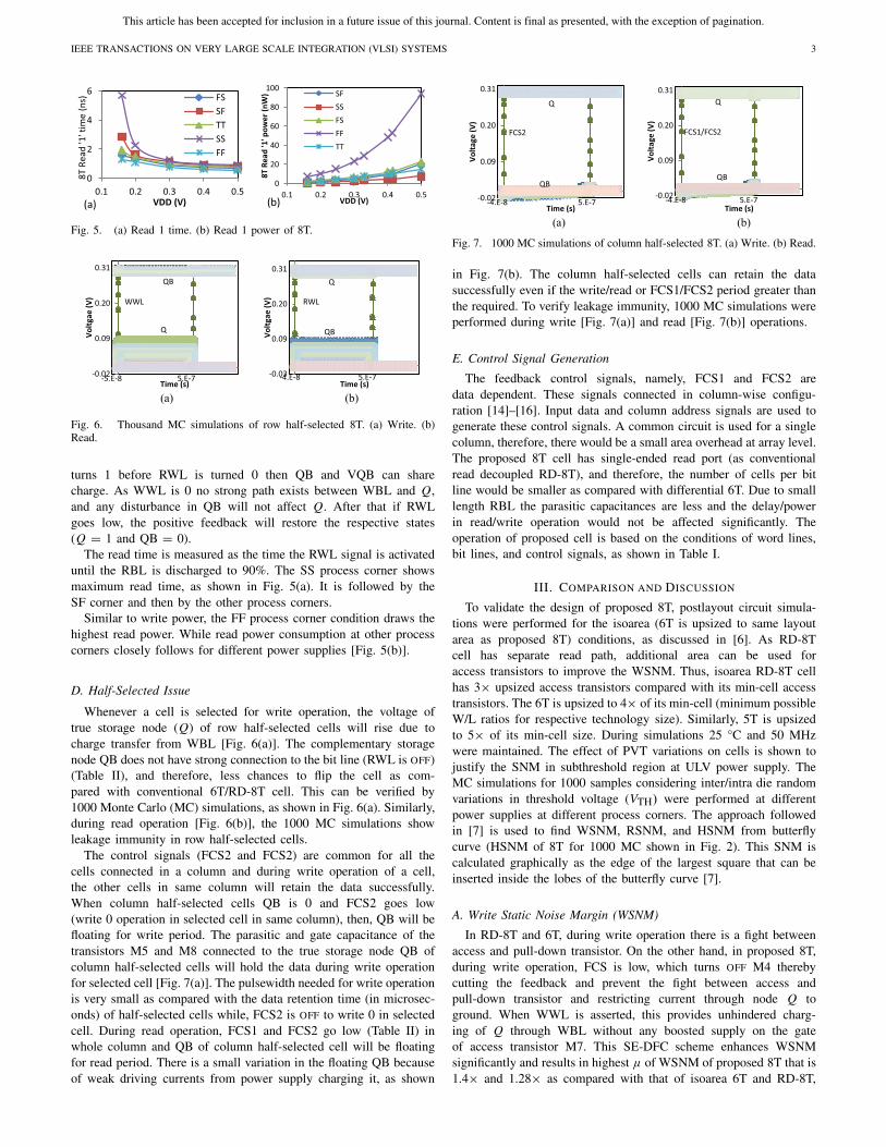
Fig. 3. (a) Write 1 time of 8T. (b) Write 0 time of 8T.
Fig. 4. (a) Write 1 power of 8T. (b) Write 0 power of 8T.
TABLE IIOPERATION TABLE OF PROPOSED 8T SRAM CELL
pMOS M1 charges QB to 1. The WT is measured as the time takenby WWL signal-to-rise to VDD/2 until the storage nodes intersecteach other. The simulations for WT were performed at all processcorners. The WT (for write 1 and write 0) for 8T increases (Fig. 3)with the decrease in power supply. The WT is highest for slow nMOSand slow pMOS (SS) worst case corner, as shown in Fig. 3(a) and (b).During write 1/0 operation, the power consumption of 8T is highestfor fast nMOS and fast pMOS (FF) process corner dominated by thefast switching activities (Fig. 4). As write 0 operation is faster thanwrite 1, the write 0 power consumption during write 0 is more ascompared with that of write 1 [Fig. 4(a) and (b)].
C. Read Operation
The read operation is performed by precharging the RBL andactivating RWL. If 1 is stored at node Q then, M4 turns ON andmakes a low resistive path for the flow of cell current throughRBL to ground. This discharges RBL quickly to ground, whichcan be sensed by the full swing inverter sense amplifier. SinceWWL, FCS1, and FCS2 were made low during the read operation(Table II), therefore, there is no direct disturbance on true storingnode QB during reading the cell. The low going FCS2 leaves QBfloating, which goes to a negative value then comes back to itsoriginal 0 value after successful read operation. If Q is high then,the size ratio of M3 and M4 will govern the read current and thevoltage difference on RBL. During read 0 operation, Q is 0 andRBL holds precharged high value and the inverter sense amplifiergives 0 at output. Since M2 is OFF so virtual QB (VQB) isisolated from QB and this prevents the chance of disturbance inQB node voltage which ultimately reduces the read failure probabilityand improves the RSNM. During read operation, if FCS1/FCS2
This article has been accepted for inclusion in a future issue of this journal. Content is final as presented, with the exception of pagination.
IEEE TRANSACTIONS ON VERY LARGE SCALE INTEGRATION (VLSI) SYSTEMS 3
Fig. 5. (a) Read 1 time. (b) Read 1 power of 8T.
Fig. 6. Thousand MC simulations of row half-selected 8T. (a) Write. (b)Read.
turns 1 before RWL is turned 0 then QB and VQB can sharecharge. As WWL is 0 no strong path exists between WBL and Q,and any disturbance in QB will not affect Q. After that if RWLgoes low, the positive feedback will restore the respective states(Q = 1 and QB = 0).
The read time is measured as the time the RWL signal is activateduntil the RBL is discharged to 90%. The SS process corner showsmaximum read time, as shown in Fig. 5(a). It is followed by theSF corner and then by the other process corners.
Similar to write power, the FF process corner condition draws thehighest read power. While read power consumption at other processcorners closely follows for different power supplies [Fig. 5(b)].
D. Half-Selected Issue
Whenever a cell is selected for write operation, the voltage oftrue storage node (Q) of row half-selected cells will rise due tocharge transfer from WBL [Fig. 6(a)]. The complementary storagenode QB does not have strong connection to the bit line (RWL is OFF)(Table II), and therefore, less chances to flip the cell as com-pared with conventional 6T/RD-8T cell. This can be verified by1000 Monte Carlo (MC) simulations, as shown in Fig. 6(a). Similarly,during read operation [Fig. 6(b)], the 1000 MC simulations showleakage immunity in row half-selected cells.
The control signals (FCS2 and FCS2) are common for all thecells connected in a column and during write operation of a cell,the other cells in same column will retain the data successfully.When column half-selected cells QB is 0 and FCS2 goes low(write 0 operation in selected cell in same column), then, QB will befloating for write period. The parasitic and gate capacitance of thetransistors M5 and M8 connected to the true storage node QB ofcolumn half-selected cells will hold the data during write operationfor selected cell [Fig. 7(a)]. The pulsewidth needed for write operationis very small as compared with the data retention time (in microsec-onds) of half-selected cells while, FCS2 is OFF to write 0 in selectedcell. During read operation, FCS1 and FCS2 go low (Table II) inwhole column and QB of column half-selected cell will be floatingfor read period. There is a small variation in the floating QB becauseof weak driving currents from power supply charging it, as shown
Fig. 7. 1000 MC simulations of column half-selected 8T. (a) Write. (b) Read.
in Fig. 7(b). The column half-selected cells can retain the datasuccessfully even if the write/read or FCS1/FCS2 period greater thanthe required. To verify leakage immunity, 1000 MC simulations wereperformed during write [Fig. 7(a)] and read [Fig. 7(b)] operations.
E. Control Signal Generation
The feedback control signals, namely, FCS1 and FCS2 aredata dependent. These signals connected in column-wise configu-ration [14]–[16]. Input data and column address signals are used togenerate these control signals. A common circuit is used for a singlecolumn, therefore, there would be a small area overhead at array level.The proposed 8T cell has single-ended read port (as conventionalread decoupled RD-8T), and therefore, the number of cells per bitline would be smaller as compared with differential 6T. Due to smalllength RBL the parasitic capacitances are less and the delay/powerin read/write operation would not be affected significantly. Theoperation of proposed cell is based on the conditions of word lines,bit lines, and control signals, as shown in Table I.
III. COMPARISON AND DISCUSSION
To validate the design of proposed 8T, postlayout circuit simula-tions were performed for the isoarea (6T is upsized to same layoutarea as proposed 8T) conditions, as discussed in [6]. As RD-8Tcell has separate read path, additional area can be used foraccess transistors to improve the WSNM. Thus, isoarea RD-8T cellhas 3× upsized access transistors compared with its min-cell accesstransistors. The 6T is upsized to 4× of its min-cell (minimum possibleW/L ratios for respective technology size). Similarly, 5T is upsizedto 5× of its min-cell size. During simulations 25 °C and 50 MHzwere maintained. The effect of PVT variations on cells is shown tojustify the SNM in subthreshold region at ULV power supply. TheMC simulations for 1000 samples considering inter/intra die randomvariations in threshold voltage (VTH) were performed at differentpower supplies at different process corners. The approach followedin [7] is used to find WSNM, RSNM, and HSNM from butterflycurve (HSNM of 8T for 1000 MC shown in Fig. 2). This SNM iscalculated graphically as the edge of the largest square that can beinserted inside the lobes of the butterfly curve [7].
A. Write Static Noise Margin (WSNM)
In RD-8T and 6T, during write operation there is a fight betweenaccess and pull-down transistor. On the other hand, in proposed 8T,during write operation, FCS is low, which turns OFF M4 therebycutting the feedback and prevent the fight between access andpull-down transistor and restricting current through node Q toground. When WWL is asserted, this provides unhindered charg-ing of Q through WBL without any boosted supply on the gateof access transistor M7. This SE-DFC scheme enhances WSNMsignificantly and results in highest μ of WSNM of proposed 8T that is1.4× and 1.28× as compared with that of isoarea 6T and RD-8T,
This article has been accepted for inclusion in a future issue of this journal. Content is final as presented, with the exception of pagination.
4 IEEE TRANSACTIONS ON VERY LARGE SCALE INTEGRATION (VLSI) SYSTEMS
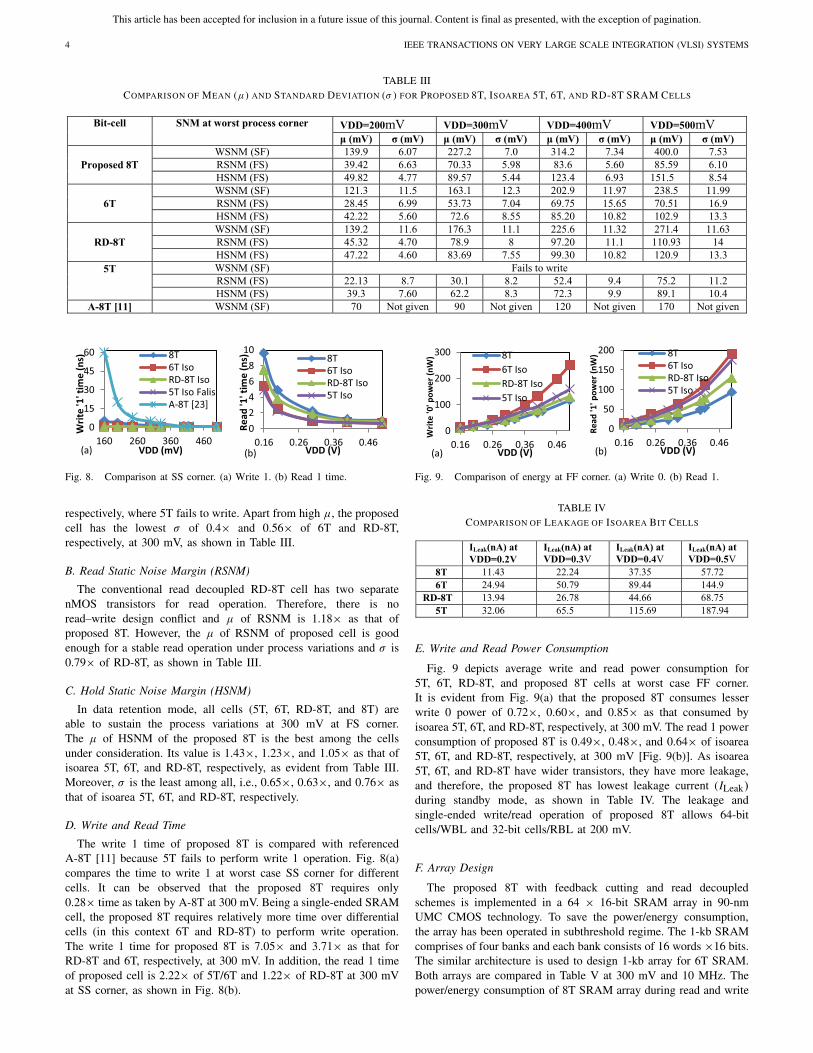
TABLE IIICOMPARISON OF MEAN (μ) AND STANDARD DEVIATION (σ ) FOR PROPOSED 8T, ISOAREA 5T, 6T, AND RD-8T SRAM CELLS
Fig. 8. Comparison at SS corner. (a) Write 1. (b) Read 1 time.
respectively, where 5T fails to write. Apart from high μ, the proposedcell has the lowest σ of 0.4× and 0.56× of 6T and RD-8T,respectively, at 300 mV, as shown in Table III.
B. Read Static Noise Margin (RSNM)
The conventional read decoupled RD-8T cell has two separatenMOS transistors for read operation. Therefore, there is noread–write design conflict and μ of RSNM is 1.18× as that ofproposed 8T. However, the μ of RSNM of proposed cell is goodenough for a stable read operation under process variations and σ is0.79× of RD-8T, as shown in Table III.
C. Hold Static Noise Margin (HSNM)
In data retention mode, all cells (5T, 6T, RD-8T, and 8T) areable to sustain the process variations at 300 mV at FS corner.The μ of HSNM of the proposed 8T is the best among the cellsunder consideration. Its value is 1.43×, 1.23×, and 1.05× as that ofisoarea 5T, 6T, and RD-8T, respectively, as evident from Table III.Moreover, σ is the least among all, i.e., 0.65×, 0.63×, and 0.76× asthat of isoarea 5T, 6T, and RD-8T, respectively.
D. Write and Read Time
The write 1 time of proposed 8T is compared with referencedA-8T [11] because 5T fails to perform write 1 operation. Fig. 8(a)compares the time to write 1 at worst case SS corner for differentcells. It can be observed that the proposed 8T requires only0.28× time as taken by A-8T at 300 mV. Being a single-ended SRAMcell, the proposed 8T requires relatively more time over differentialcells (in this context 6T and RD-8T) to perform write operation.The write 1 time for proposed 8T is 7.05× and 3.71× as that forRD-8T and 6T, respectively, at 300 mV. In addition, the read 1 timeof proposed cell is 2.22× of 5T/6T and 1.22× of RD-8T at 300 mVat SS corner, as shown in Fig. 8(b).
Fig. 9. Comparison of energy at FF corner. (a) Write 0. (b) Read 1.
TABLE IVCOMPARISON OF LEAKAGE OF ISOAREA BIT CELLS
E. Write and Read Power Consumption
Fig. 9 depicts average write and read power consumption for5T, 6T, RD-8T, and proposed 8T cells at worst case FF corner.It is evident from Fig. 9(a) that the proposed 8T consumes lesserwrite 0 power of 0.72×, 0.60×, and 0.85× as that consumed byisoarea 5T, 6T, and RD-8T, respectively, at 300 mV. The read 1 powerconsumption of proposed 8T is 0.49×, 0.48×, and 0.64× of isoarea5T, 6T, and RD-8T, respectively, at 300 mV [Fig. 9(b)]. As isoarea5T, 6T, and RD-8T have wider transistors, they have more leakage,and therefore, the proposed 8T has lowest leakage current (ILeak)during standby mode, as shown in Table IV. The leakage andsingle-ended write/read operation of proposed 8T allows 64-bitcells/WBL and 32-bit cells/RBL at 200 mV.
F. Array Design
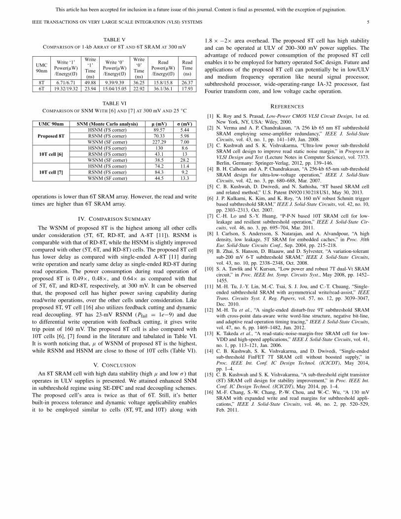
The proposed 8T with feedback cutting and read decoupledschemes is implemented in a 64 × 16-bit SRAM array in 90-nmUMC CMOS technology. To save the power/energy consumption,the array has been operated in subthreshold regime. The 1-kb SRAMcomprises of four banks and each bank consists of 16 words ×16 bits.The similar architecture is used to design 1-kb array for 6T SRAM.Both arrays are compared in Table V at 300 mV and 10 MHz. Thepower/energy consumption of 8T SRAM array during read and write
This article has been accepted for inclusion in a future issue of this journal. Content is final as presented, with the exception of pagination.
IEEE TRANSACTIONS ON VERY LARGE SCALE INTEGRATION (VLSI) SYSTEMS 5
TABLE VCOMPARISON OF 1-kb ARRAY OF 8T AND 6T SRAM AT 300 mV
TABLE VICOMPARISON OF SNM WITH [6] AND [7] AT 300 mV AND 25 °C
operations is lower than 6T SRAM array. However, the read and writetimes are higher than 6T SRAM array.
IV. COMPARISON SUMMARY
The WSNM of proposed 8T is the highest among all other cellsunder consideration (5T, 6T, RD-8T, and A-8T [11]). RSNM iscomparable with that of RD-8T, while the HSNM is slightly improvedcompared with other (5T, 6T, and RD-8T) cells. The proposed 8T cellhas lower delay as compared with single-ended A-8T [11] duringwrite operation and nearly same delay as single-ended RD-8T duringread operation. The power consumption during read operation ofproposed 8T is 0.49×, 0.48×, and 0.64× as compared with thatof 5T, 6T, and RD-8T, respectively, at 300 mV. It can be observedthat, the proposed cell has higher power saving capability duringread/write operations, over the other cells under consideration. Likeproposed 8T, 9T cell [16] also utilizes feedback cutting and dynamicread decoupling. 9T has 23-mV RSNM (Pfail = 1e−9) and dueto differential write operation with feedback cutting, it gives writetrip point of 160 mV. The proposed 8T cell is also compared with10T cells [6], [7] found in the literature and tabulated in Table VI.It is worth noticing that, μ of WSNM of proposed 8T is the highest,while RSNM and HSNM are close to those of 10T cells (Table VI).
V. CONCLUSION
An 8T SRAM cell with high data stability (high μ and low σ) thatoperates in ULV supplies is presented. We attained enhanced SNMin subthreshold regime using SE-DFC and read decoupling schemes.The proposed cell’s area is twice as that of 6T. Still, it’s betterbuilt-in process tolerance and dynamic voltage applicability enablesit to be employed similar to cells (8T, 9T, and 10T) along with
1.8 × −2× area overhead. The proposed 8T cell has high stabilityand can be operated at ULV of 200–300 mV power supplies. Theadvantage of reduced power consumption of the proposed 8T cellenables it to be employed for battery operated SoC design. Future andapplications of the proposed 8T cell can potentially be in low/ULVand medium frequency operation like neural signal processor,subthreshold processor, wide-operating-range IA-32 processor, fastFourier transform core, and low voltage cache operation.
REFERENCES
[1] K. Roy and S. Prasad, Low-Power CMOS VLSI Circuit Design, 1st ed.New York, NY, USA: Wiley, 2000.
[2] N. Verma and A. P. Chandrakasan, “A 256 kb 65 nm 8T subthresholdSRAM employing sense-amplifier redundancy,” IEEE J. Solid-StateCircuits, vol. 43, no. 1, pp. 141–149, Jan. 2008.
[3] C. Kushwah and S. K. Vishvakarma, “Ultra-low power sub-thresholdSRAM cell design to improve read static noise margin,” in Progress inVLSI Design and Test (Lecture Notes in Computer Science), vol. 7373.Berlin, Germany: Springer-Verlag, 2012, pp. 139–146.
[4] B. H. Calhoun and A. P. Chandrakasan, “A 256-kb 65-nm sub-thresholdSRAM design for ultra-low-voltage operation,” IEEE J. Solid-StateCircuits, vol. 42, no. 3, pp. 680–688, Mar. 2007.
[5] C. B. Kushwah, D. Dwivedi, and N. Sathisha, “8T based SRAM celland related method,” U.S. Patent IN920 130 218 US1, May 30, 2013.
[6] J. P. Kulkarni, K. Kim, and K. Roy, “A 160 mV robust Schmitt triggerbased subthreshold SRAM,” IEEE J. Solid-State Circuits, vol. 42, no. 10,pp. 2303–2313, Oct. 2007.
[7] C.-H. Lo and S.-Y. Huang, “P-P-N based 10T SRAM cell for low-leakage and resilient subthreshold operation,” IEEE J. Solid-State Cir-cuits, vol. 46, no. 3, pp. 695–704, Mar. 2011.
[8] I. Carlson, S. Andersson, S. Natarajan, and A. Alvandpour, “A highdensity, low leakage, 5T SRAM for embedded caches,” in Proc. 30thEur. Solid-State Circuits Conf., Sep. 2004, pp. 215–218.
[9] B. Zhai, S. Hanson, D. Blaauw, and D. Sylvester, “A variation-tolerantsub-200 mV 6-T subthreshold SRAM,” IEEE J. Solid-State Circuits,vol. 43, no. 10, pp. 2338–2348, Oct. 2008.
[10] S. A. Tawfik and V. Kursun, “Low power and robust 7T dual-Vt SRAMcircuit,” in Proc. IEEE Int. Symp. Circuits Syst., May 2008, pp. 1452–1455.
[11] M.-H. Tu, J.-Y. Lin, M.-C. Tsai, S. J. Jou, and C.-T. Chuang, “Single-ended subthreshold SRAM with asymmetrical write/read-assist,” IEEETrans. Circuits Syst. I, Reg. Papers, vol. 57, no. 12, pp. 3039–3047,Dec. 2010.
[12] M.-H. Tu et al., “A single-ended disturb-free 9T subthreshold SRAMwith cross-point data-aware write word-line structure, negative bit-line,and adaptive read operation timing tracing,” IEEE J. Solid-State Circuits,vol. 47, no. 6, pp. 1469–1482, Jun. 2012.
[13] K. Takeda et al., “A read-static-noise-margin-free SRAM cell for low-VDD and high-speed applications,” IEEE J. Solid-State Circuits, vol. 41,no. 1, pp. 113–121, Jan. 2006.
[14] C. B. Kushwah, S. K. Vishvakarma, and D. Dwivedi, “Single-endedsub-threshold FinFET 7T SRAM cell without boosted supply,” inProc. IEEE Int. Conf. IC Design Technol. (ICICDT), May 2014,pp. 1–4.
[15] C. B. Kushwah and S. K. Vishvakarma, “A sub-threshold eight transistor(8T) SRAM cell design for stability improvement,” in Proc. IEEE Int.Conf. IC Design Technol. (ICICDT), May 2014, pp. 1–4.
[16] M.-F. Chang, S.-W. Chang, P.-W. Chou, and W.-C. Wu, “A 130 mVSRAM with expanded write and read margins for subthreshold appli-cations,” IEEE J. Solid-State Circuits, vol. 46, no. 2, pp. 520–529,Feb. 2011.