Embed Size (px)
Citation preview
ISI Research Reporl i
ISI/RR-89-230X)P April 1989
N Universit)'
of Southern_California .
Shih-Lien Lu
A Single-Phase Clocked NOR/NOR CMOSProgrammable Sequential Array Structure
DTICAO ELECTE
l---AUG16 1989
Approved for public n~aemin
INFORMATIONSCIENCES 213/822-1511
INSTITUTE't"--" i-4676 Admiralty Way/MAarina del Rey/California 90292-65
89 8 15 056

UnclastMed
SECURITY CLASSIFICATION OF THIS PAGE
REPORT DOCUMENTATION PAGE1. REPORT SECURITY CLASSIFICATION lb. RESTRICTIVE MARKINGS
Unclassified2@. SECURITY CLASSIFICATION AUTHORITY ". DISTRIOUTION/AVAILABILITY OF REPORT
2b. DECLASSIFICATION/DOWNGRADING SCHEDULE This document Is approved for public release;distribution is unlimited.
4. PERFORMING ORGANIZATION REPORT NUMBER(S) S. MONITORING ORGANIZATION REPORT NUMBER(S)
ISI/RR-89-230
6,. NAME OF PERFORMING ORGANIZATION "6b. OFFICE SYMBOL 7,. NAME OF MONITORING ORGANIZATION
USC/Information Sciences Institute (I applicable)
6c. ADDRESS (Oty, State, and ZIP Code) 7b. ADDRESS (City, State, and ZIP Code)
4676 Admiralty WayMarina del Rey, CA 90292-6695
Ba. NAME OF FUNDING/SPONSORING NSF Ib. OFFICE SYMBOL 9. PROCUREMENT INSTRUMENT IDENTIFICATION NUMBERORGANIZATION Defense (if app cable) NI DA903-86-C-0178 F2960 I-87-C-0069Advanced Research Projects Agency I
Sc. ADDRESS (City, State, and ZIP Code) 10. SOURCE OF FUNDING NUMBERS
DARPA National Science Foundation PROGRAM PROJECT TASK WORK UNIT1400 \Vilson Boulevard ISOO C; StL'Cet N\V ELEMENT NO. NO. NO. IACCESSION NO.Arlington, VA 22209 \Vashington, DC 20550- ----- - --- - - - -
11. TITLE (Include Security Classification)
A Single-Phase Clocked NOR/NOR CMOS Programmable Sequential Array Structure (Unclassified)
12. PERSONAL AUTHOR(S) Lu, Shih-Lien
13a. TYPE OF REPORT 13b. TIME COVERED 114. DATE OF REPORT (Year, Month, Day) 1S. PAGE COUNTResearch Report FROM TO_ 1989, April 14
16. SUPPLEMENTARY NOTATION
17. COSATI CODES 18. SUBJECT TERMS (Continue on reverse ff necessary and identify by block number)FIELD GROUP SUB-GROUP CN[OS, combinational locic, IOSIS, NOR/NOR, integrated circuit design,
09 02 programmable logic arrays, sin-wlc-phase clocking, \;LSI
19. ABSTRACT (Continue on reverse f necessary and Identify by block number)
- A static CMOS Programmable Sequential Array (PSA) structure is presented, which uses a prechargeCMOS NOR/NOR logic structure to implement combinational logic. It is fast, it consumes no staticpower, and it imposes no limits on the number of input terms. Only one input clock is required whileadditional clocks are generated by the PSA structure. Static latches are added to the output. Results willremain unchanged with the absence of a high clock signal. This single-phase clocking technique, withstatistically latched outputs, permits this proposed PSA to be used for many different system overall timingstrategies. The proposed methodology has been implemented with MOSIS scalable design rules (rev. 6)and has been adapted into the Berkeley VLSI CAD tool system--MPLA's tiling format. An automaticallygenerated example is given.
i
20. DISTRIBUTION/AVAILABILITY OF ABSTRACT 21. ABSTRACT SECURITY CLASSIFICATIONIUNCLASSIFIEDIUNLIMITED I SAME AS RPT. I DTIC USERS Unclassified
22a. NAME OF RESPONSIBLE INDIVIDUAL 22b. TELEPHONE ("cude Area Code) 22. OFFICE SYMBOLVictor Brown Sheila Coyazo 213/822-1511
DO FORM 1473,64 MAR 63 APR dion may be used until exhausted. SECURITY CLASSIFICATION OF THIS PAGEAll other editions are obsolete. U nclasified
Unclassified
1SI Research ReportISI/RR-89-230
April 1989
of Soulhern , ' 1California
L
Shih-Lien Lu
%%X%..... XA Single-Phase Clocked NOR/NOR CMOSProgrammable Sequential Array Structure
INFORMATIONSCIENCES 213/822-1511INSTITUTEJ I 4676 Admiralty Way/Marina del Rey/California 90292-6695
This research is supported by the Defense Advanced Research Projects Agency under Contract No. MDA903-86-C-0178 and by theNotional Sc ence Foundation under Contract No. F29601-87-C-0069. Views and conclusions contained In this report are those of theauthor an. should not be interpreted as representing the official opinion or policy of DARPA. NSF, the U.S. Government, or any personor agency connected with them.
I. Introduction
Programmable logic arrays (PLAs) provide an efficient and flexible way to implement general
modules for combinational systems in a regular manner. Similarly programmable sequential
arrays can be formed by including storage cells together with the logic. These arrays can be
programmed to implement general modules of sequential systems. While implementing
Boolean functions with PLAs, a general logic function is first represented in a
sum-of-products terms. Then, a two-stage NOR network (with NOT function added to both
input and output) is used to map the logic equation to gates.
While nMOS realization of NOR gates is quite good and straightforward, static CMOS/bulk
NOR gates present many problems [1]. First, while the better devices (n-channels) are in
parallel, the worse devices (p-channels) are in series, which makes the gate slow. In fact, an
NAND/NAND structure is generally used, which puts the better devices (n-channels) in
series. Second, since both n-channel devices and p-channel devices are required, well
location must be carefully arranged and the total area needed is large. Domino CMOS [21
r ethod is used to implement small precharge PLAs in CMOS/bulk. The standard approach
is to use a precharge NAND structure to implement the AND plane of the PLA and to use a
precharge NOR to implement the OR plane. In between the planes and at output NOT is
used. This approach is nice because there is no charge sharing possibility in precharge NOR
gates. However the main disadvantage of thi,, i ino PLA is that with large input terms, the
series AND in the NAND gates is still slow. L, t, the delay is quadratic in the number of
literals in series. As a result, it is desirable to have a precharge NOR/NOR typed of PLA
structures in CMOS. Unfortunately, the precharge NOR gate cannot be concatenated directly
to form a NOR/NOR PLA structure. This is a result of having the output of a precharge NOR
gate goes from one to NOR. If this output is directly connected to the input of another
precharge NOR gate undesired discharging will occur.
ForThus, one must include some timing strategy to prevent unwanted discharging. In this paper, I
delayed clock is used to precharge the OR plane, which allows the concatenation of NOR 1 C
gates. We will discuss the circuit and its timing strategy in the following sections. This PLA - a
structure has been adapted into Berkeley PLA tools [3]. Optimization and auto-generation
of general Finite State Machine (FSM) is available to the public. 1/
ity CodesAvail arid/or
iDist Special1L m....
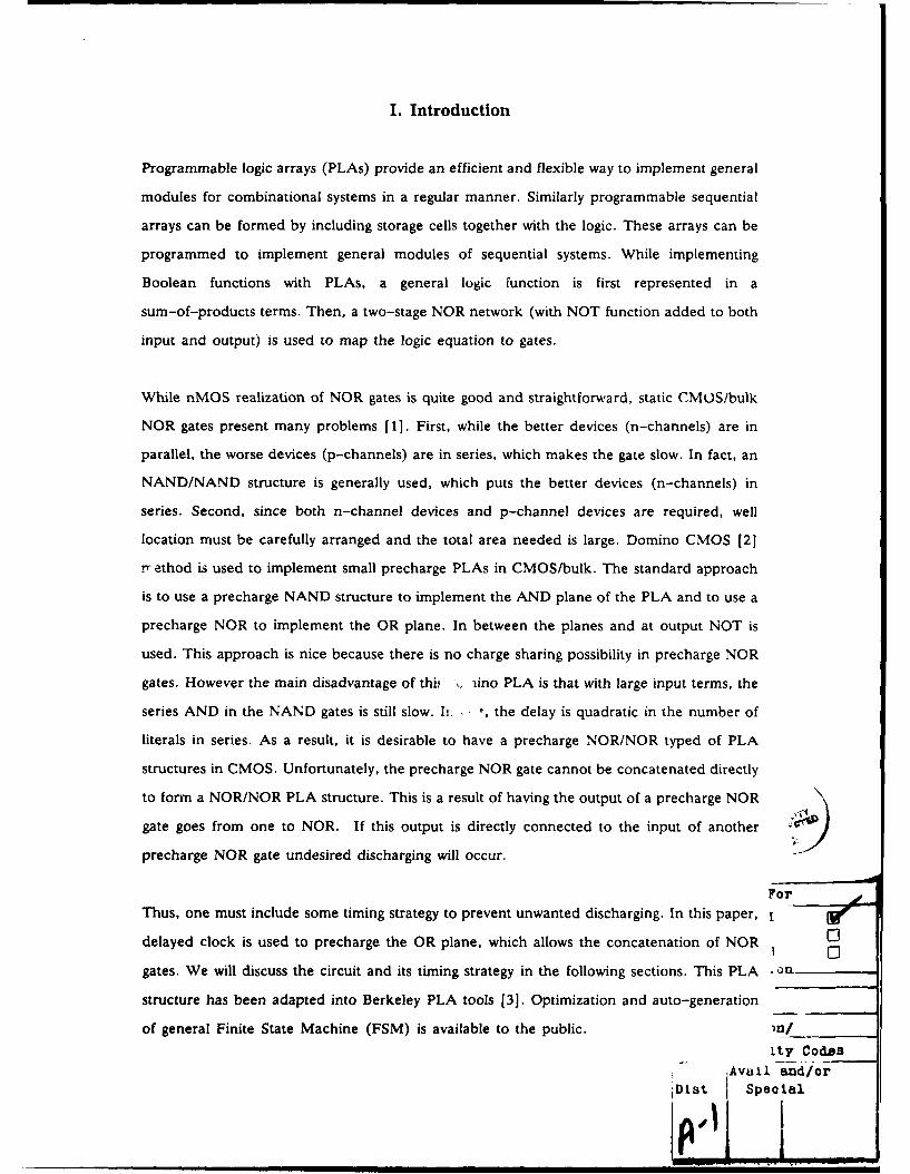
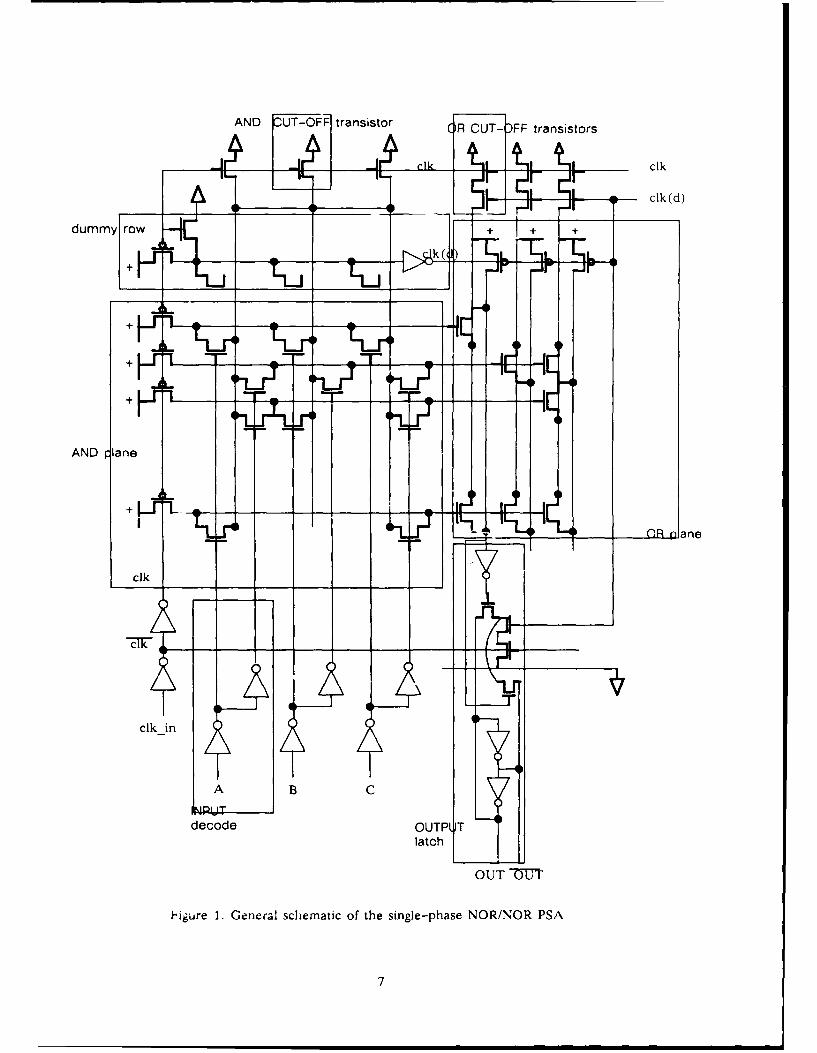
II. Circuit Description
Several dynamic CMOS NOR/NOR PLA structures have been suggested [1] [4] 151 [6] [9].
The proposed approach is similar to [4]. A schematic diagram of the circuitry is shown in
Figure 1. The AND plane consists of the normal precharge NOR gates arranges as one row
per implicants. It is precharged during the low clock signal and it is evaluated when the clock
signal is high. On the top of the AND plane is a dummy row. For each of the input literals, a
diffusion area equals to the drain area of a pull-down transistor is added to the dummy row.
As a result the total parasitic loading on the dummy row is greater than any of the implicant
row. Since it is also precharged by the same clock signal as the rest of the implicants, it
discharges at the worst-case rate in comparison with the rest of the rows. This slowest
"dummy-implicant" is inverted to produce the delayed clock. This delayed clock is then
used to precharge and evaluate the OR plane NOR gates. By the time this delayed clock rises
to evaluate the OR plane logic, all implicants has settled to its desired output of either high or
low state. Hence, no undesirable discharging by the OR plane NOR gates can occur. Outputs
from the OR plane NOR gates are latched by static flip-flops. These flip-flops are gated by
the inverse of the input clock and the delayed clock. In effect, the latched output will change
its state only after the trailing edge of the input clock signal. This will warrant no undesirable
discharging when concatenating blocks of these PSA. Moreover, this PSA structure is static
from a system point of view.
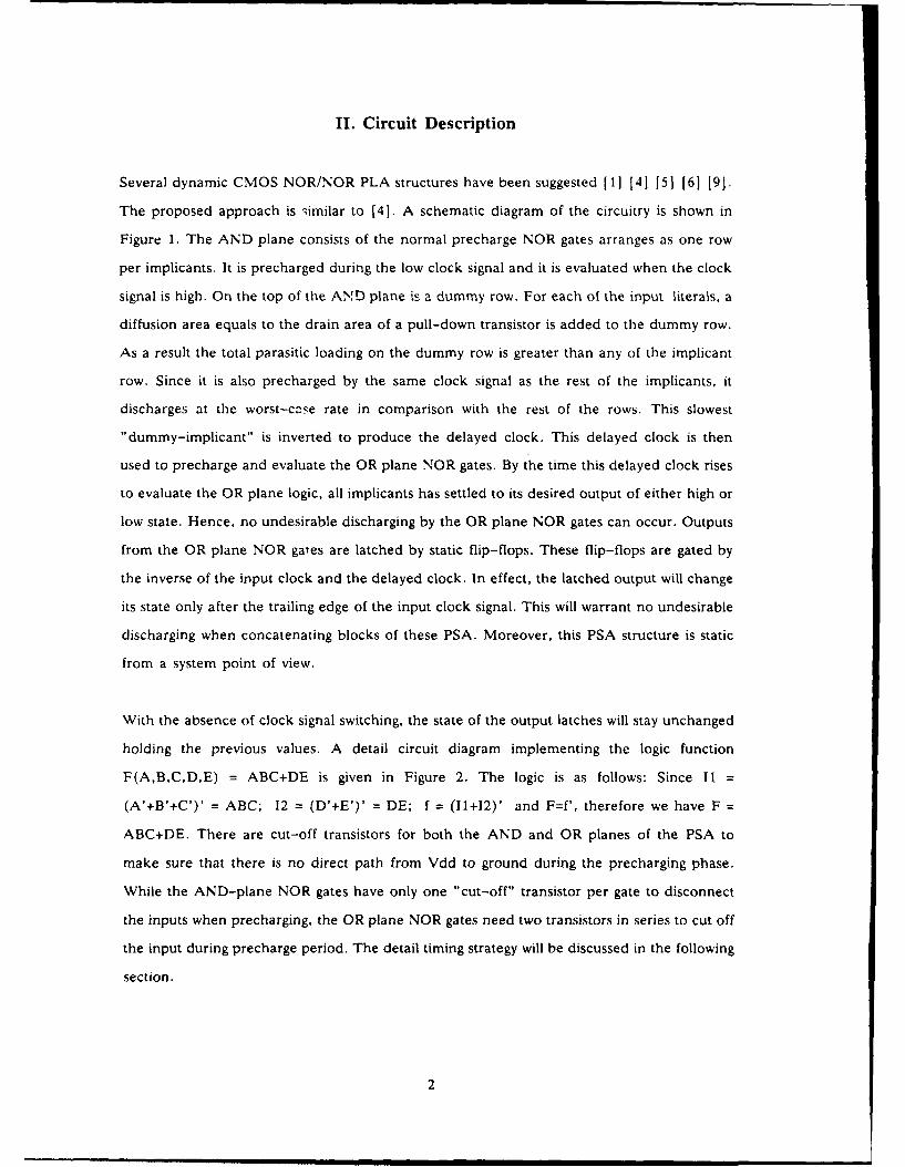
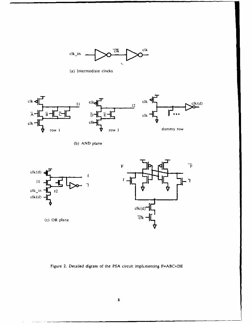
With the absence of clock signal switching, the state of the output latches will stay unchanged
holding the previous values. A detail circuit diagram implementing the logic function
F(A,B,C,D,E) = ABC+DE is given in Figure 2. The logic is as follows: Since I1 =
(A'+B'+C')' = ABC; 12 = (D'+E')' = DE; f = (11+12)' and F=f', therefore we have F =
ABC+DE. There are cut-off transistors for both the AND and OR planes of the PSA to
make sure that there is no direct path from Vdd to ground during the precharging phase.
While the AND-plane NOR gates have only one "cut-off" transistor per gate to disconnect
the inputs when precharging, the OR plane NOR gates need two transistors in series to cut off
the input during precharge period. The detail timing strategy will be discussed in the following
section.
2
III. Timing and Electrical Design Consideration
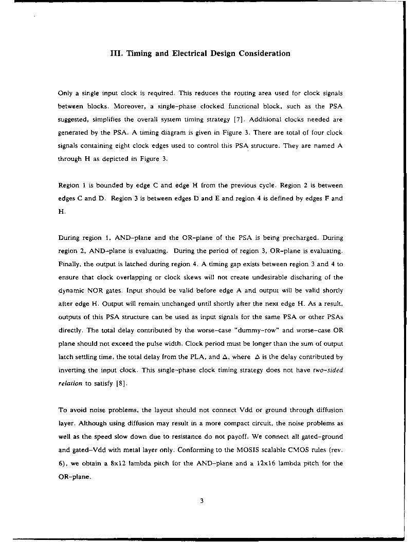
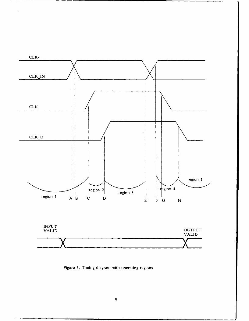
Only a single input clock is required. This reduces the routing area used for clock signals
between blocks. Moreover, a single-phase clocked functional block, such as the PSA
suggested, simplifies the overall system timing strategy [7]. Additional clocks needed are
generated by the PSA. A timing diagram is given in Figure 3. There are total of four clock
signals containing eight clock edges used to control this PSA structure. They are named A
through H as depicted in Figure 3.
Region 1 is bounded by edge C and edge H from the previous cycle. Region 2 is between
edges C and D. Region 3 is between edges D and E and region 4 is defined by edges F and
H.
During region 1, AND-plane and the OR-plane of the PSA is being precharged. During
region 2, AND-plane is evaluating. During the period of region 3, OR-plane is evaluating.
Finally, the output is latched during region 4. A timing gap exists between region 3 and 4 to
ensure that clock overlapping or clock skews will not create undesirable discharing of the
dynamic NOR gates. Input should be valid before edge A and output will be valid shortly
after edge H. Output will remain unchanged until shortly after the next edge H. As a result,
outputs of this PSA structure can be used as input signals for the same PSA or other PSAs
directly. The total delay contributed by the worse-case "dummy-row" and worse-case OR
plane should not exceed the pulse width. Clock period must be longer than the sum of output
latch settling time, the total delay from the PLA, and A, where A is the delay contributed by
inverting the input clock. This single-phase clock timing strategy does not have two-sided
relation to satisfy [8].
To avoid noise problems, the layout should not connect Vdd or ground through diffusion
layer. Although using diffusion may result in a more compact circuit, the noise problems as
well as the speed slow down due to resistance do not payoff. We connect all gated-ground
and gated-Vdd with metal layer only. Conforming to the MOSIS scalable CMOS rules (rev.
6), we obtain a 8x12 lambda pitch for the AND-plane and a 12x16 lambda pitch for the
OR-plane.
3
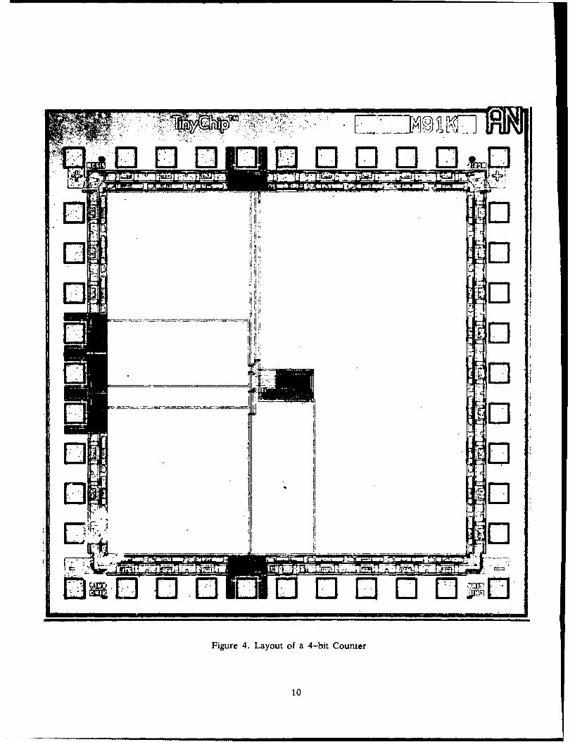
IV. Example
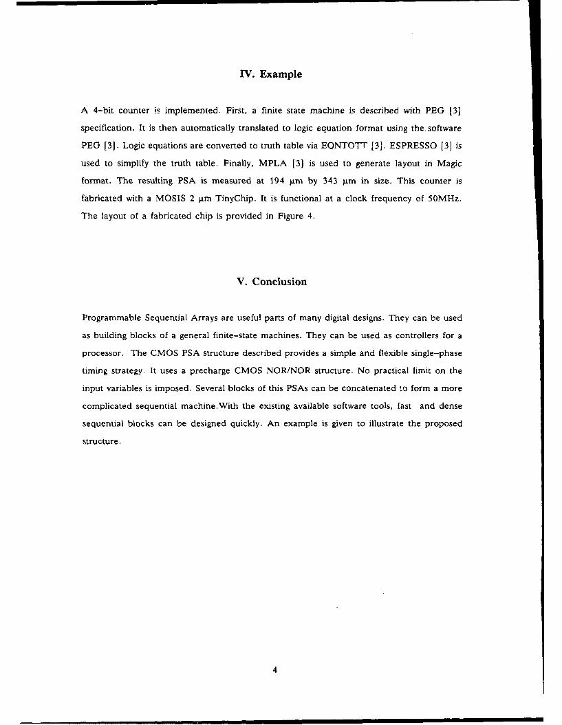
A 4-bit counter is implemented. First, a finite state machine is described with PEG [3]
specification. It is then automatically translated to logic equation format using the~software
PEG [3]. Logic equations are converted to truth table via EQNTOTT [3]. ESPRESSO [3] is
used to simplify the truth table. Finally, MPLA [3] is used to generate layout in Magic
format. The resulting PSA is measured at 194 A±m by 343 gm in size. This counter is
fabricated with a MOSIS 2 ;im TinyChip. It is functional at a clock frequency of 50MHz.
The layout of a fabricated chip is provided in Figure 4.
V. Conclusion
Programmable Sequential Arrays are useful parts of many digital designs. They can be used
as building blocks of a general finite-state machines. They can be used as controllers for a
processor. The CMOS PSA structure described provides a simple and flexible single-phase
timing strategy. It uses a precharge CMOS NOR/NOR structure. No practical limit on the
input variables is imposed. Several blocks of this PSAs can be concatenated to form a more
complicated sequential machine.With the existing available software tools, fast and dense
sequential blocks can be designed quickly. An example is given to illustrate the proposed
structure.
4
Acknowledgment
The author would like to thank Dr. G. Lewicki for his encouragement and many helpful
discussions.
References
1. C. Seitz, Lecture notes, 1985 VLSI teacher's course.
2. R. H. Krambeck, C. M. Lee and H. S, Law, "High-Speed Compact Circuits with
CMOS," IEEE Journal of Solid-State Circuits, Vol. SC-17, June 1982, pp. 614-619.
3. W. S. Scott, R. N. Mayo, G. Hamachi and J. K. Ousterhout, editors, "1986 VLSITools: Still More Works by the Original Artists," Manuals of the Berkeley VLSITools. Department of Electrical Engineering and Computer Science, University of
California, Berkeley.
4. N. Weste, Principles of CMOS VLSI Design: A System Perspective, Addison-WesleyPublishing Company, 1985.
5. H-F. S. Law and M. Shoji, "PLA Design for the BELLMAC-32A Microprocessor,"Proceedings of the ICCC, 1982, pp. 161-164.
6. E. Hebenstreit and K. Horninger, "High-Speed Programmable Logic Arrays in ESFISOS Technology," IEEE Journal of Solid-State Circuits, Vol. SC-11, No. 3, June1976, pp. 370-374.
7. S. H. Unger and C.-J. Tan, "Clocking Schemes for High-Speed Digital Systems,"
IEEE Transactions on Computing, Vol. C-35, No. 10, October 1986, pp. 880-895.
8. C. Mead and L. Conway, Introduction to VLSI Systems, Addison-Wesley Publishing
Company, 1980.
9. D. L. Liu and E. J. McCluskey, "Design of Large Embedded CMOS PLAs forBuilt-in Self-Test," Proceedings of the ICCD, 1987, pp. 678-681.
5
List of Figures
Figure 1. A general schematic diagram of the single-phase NOR/NOR PSA
Figure 2. An Example PSA Implementing F=ABC+DE
Figure 3. Timing Diagram with Operating Regions
Figure 4. Layout of a 4-bit Counter
b
AN U -F rnsso RC T DF rnitr
1- rk l
cikk in
decodeIdummy roat+h
OTL F YJ L
+ -gr .Gnrlshmtcoftesnl-hs O/O S
Ili LLJ 7
cik in
(a) Intermediate clocks
clk. clkj 12 clk clk (d)
'A bA CADlE ckc~E clH
ck row 1 lk row Idummy row
(b) AND plane
F F
clk(d)f
1~ f1
clkinj 12
clk(d)
(c) OR plane M
Figure 2. Detailed dligram of the PSA circuit implcmenting F=ABC+DE
8
CLK-
CLK
region I
egir. 2regin 3gion 4
region 1 A B C D E T
INPUTVALID OUTPUT
VALID
Figure 3. Timing diagram with operating regions
9
'PI~
IL'E-
Figure 4. Layout of a 4-bit Counter
10


![INDEX [wakerly.org]wakerly.org/DDPP/DDPP3_mkt/ddpp3ix.pdf · INDEX Note: Page numbers for ... clocked assignment operator, := 628 clocked truth-table operator, :> 628 ... 243 Brayton,](https://img.pdfslide.net/doc/110x75/5ace2c0d7f8b9a93268e77ed/index-note-page-numbers-for-clocked-assignment-operator-628-clocked.jpg)