Embed Size (px)
Citation preview
A SPREAD SPECTRUM COMMUNICATION SYSTEM
Cain Garrett

Library
Naval Postgraduate School
Monterey, California 93940
NAVAL POSTGRADUATE SCHOOL
Monterey, California
THESIS. A SPREAD SPECTRUM COMMUNICATION SYSTEM
by
Cain Garrett, Jr,
December 1974
Thesis Advisor: S. Jauregui
Approved for public release; distribution unlimited.
T.164029

UNCLASSIFIEDSECURITY CLASSIFICATION OF THIS PAGE (Whmn D<tt« Entered)
REPORT DOCUMENTATION PAGEt. REPORT NUMBER 2. GOVT ACCESSION NO
READ INSTRUCTIONSBEFORE COMPLETING FORM
3. RECIPIENT'S CATALOG NUMBER
4. TITLE (end Subtitle)
A Spread Spectrum Communication System
5. TYPE OF REPORT ft. PERIOO COVEREDElectrical Engineer;December 1974« PERFORMING ORG. REPORT NUMBER
7. AUTHOR^.)
Cain Garrett, Jr.
S. CONTRACT OR GRANT NUMBERS
9. PERFORMING ORGANIZATION NAME AND AODRESS
Naval Postgraduate SchoolMonterey, California 93940
10. PROGRAM ELEMENT. PROJECT, TASKAREA & WORK UNIT NUMBERS
II. CONTROLLING OFFICE NAME AND ADDRESS
Naval Postgraduate SchoolMonterey, California 93940
12. REPORT DATE
December 197413. NUMBER OF PAGES
8614. MONITORING AGENCY NAME 4 AODRESSf// different Irom Controlling Ottlcei
Naval Postgraduate SchoolMonterey, California 93940
IS. SECURITY CLASS, (ol thle riport)
Unclassified
15a. DECLASSIFI CATION/ DOWN GRADINGSCHEDULE
16. DISTRIBUTION STATEMENT (ol thla Report;
Approved for public release; distribution unlimited,
17. DISTRIBUTION STATEMENT (ol the ebetrect entered In Block 30, II different Irom Report)
18. SUPPLEMENTARY NOTES
19- KEY WORDS (Continue on revere* elde It neceeeery end Identity by block number)
Spread SpectrumSpread Spectrum CommunicationsAcoustic Surface Wave DeviceGolay Coding
20. ABSTRACT (Continue on r*v«ra« elde It neceeeery end Identity by block number)
This thesis reports on an investigation of a practicalsolution to the problem of providing covert, secure protectionto the video channel of a remotely piloted vehicle (RPV) down-link. Spread spectrum technology employing acoustic surfacewave devices and Golay complementary code sequences areutilized. Bandwidth reduction of the video data to a datarate of 200 kilobits per second is assumed.
DD I JAN*73 1473 EDITION OF I NOV 6S IS OBSOLETE
(Page 1) S' N oios-014-6601 i
1
UNCLASSIFIEDSECURITY CLASSIFICATION OF THIS PACE (When Dele Bnlered)

UNCLASSIFIEDt'kCIJWITY CLASSIFICATION OF THIS P»OE,rWTi»n D«<« Cnltii:'
Block #19 Continued
ASWDRemotely Piloted VehicleVideo Data LinkImagery TransmissionTransmitter/ReceiverWideband AmplifiersProcessing GainCovert Communications
Block #20 Continued
A discussion of the need for such a system and thequalities that a successful system should possess is in-cluded in the introduction. Problems inherent in providingan adequate video link for military RPV usage are examined.
The thesis effort results in a transmitter/receivercombination with many of the desirable qualities of avideo link for military RPV employment in a hostile en-vironment. The hardware contains modifications that weremade to facilitate system testing. Tests results arereported.
The emphasis of the thesis is on the satisfaction ofthe system specifications through hardware implementation.
DD1 Jan
1
??H73 (BACK)
9UNCLASSIFIED
S/N 0102-014-(5601 SECURITY CLASSIFICATION OF THIS P»OEf**.n D.I. Enl.r.d)

A Spread Spectrum Communication System
by
Cain Garrett , Jr.Lieutenant Commander, United States Navy
M.S., Naval Postgraduate School, 1973
Submitted in partial fulfillment of therequirements for the degree of
ELECTRICAL ENGINEER
from the
NAVAL POSTGRADUATE SCHOOLDecember 1974

-AG
Library
Naval Postgradua"Monterey,
iI
ABSTRACT
This thesis reports on an investigation of a practical
solution to the problem of providing covert, secure protec-
tion to the video channel of a remotely piloted vehicle
(RPV) down-link. Spread spectrum technology employing
acoustic surface wave devices and Golay complementary code
sequences are utilized. Bandwidth reduction of the video
data to a data rate of 200 kilobits per second is assumed.
A discussion of the need for such a system and the
qualities that a successful system should possess is in-
cluded in the introduction. Problems inherent in providing
an adequate video link for military RPV usage are examined.
The thesis effort results in a transmitter/receiver
combination with many of the desirable qualities of a video
link for military RPV employment in a hostile environment.
The hardware contains modifications that were made to
facilitate system testing. Tests results are reported.
The emphasis of the thesis is on the satisfaction of the
system specifications through hardware implementation.

TABLE OF CONTENTS
I. INTRODUCTION - 13
A. STATEMENT OF THE PROBLEM 16
B. DEFINING THE THESIS --- 17
1. General Considerations 18
2. Physical Considerations 19
3. Theoretical Considerations 20
II. DESIGN SPECIFICATIONS AND OBJECTIVES 22
III. SYSTEM DESIGN AND FABRICATION 24
A. CHOICE OF SPREAD SPECTRUM MODULATION SCHEME-- 24
B. ELEMENTS OF DESIGN 32
1. Modulating the Acoustic Surface WaveDevices 33
2. Multiplexing the Complementary Waveforms- 35
3. Amplification and Transmission of theMultiplexed Signal 36
4. Reception and Amplification of the SpreadSpectrum Signal 38
5. Demultiplexing and Demodulating theReceived Signal 38
IV. SYSTEM INTEGRATION - 42
A. FILTERS--- 43
B. AMPLIFIER INTERFACES -- -- 45
V. TEST PROCEDURES --- 48
A. TESTING CONSIDERATIONS 48
B. TEST SETUP FOR NARROW BAND NOISE REJECTIONMEASUREMENTS 4 9
C. TEST SETUP FOR WIDEBAND INTERFERENCEREJECTION MEASUREMENTS- 50

D. TEST EQUIPMENT AND DEVICES 51
VI. SYSTEM PERFORMANCE 52
A. SYSTEM PERFORMANCE IN VARIOUS CW JAMENVIRONMENTS 5 3
B. SYSTEM PERFORMANCE IN A WIDEBAND NOISEENVI RONMENT 54
C. DISCUSSION OF SYSTEM PERFORMANCE 54
VII. CONCLUSION 65
APPENDIX A: ACOUSTIC SURFACE WAVE DEVICES AS SPREADSPECTRUM MODULATORS 67
APPENDIX B: GOLAY COMPLEMENTARY SEQUENCES IN ASWDAPPLICATIONS 74
APPENDIX C: CHARACTERISTICS OF SYSTEM ACOUSTIC SUR-FACE WAVE DEVICES 77
APPENDIX D: SYNCHRONIZATION CONSIDERATIONS 82
LIST OF REFERENCES 84
INITIAL DISTRIBUTION LIST 85

LIST OF TABLES
1. System Performance in the Presence of a 19MHz CWJam Signal 55
2. System Performance in the Presence of a 20MHz CWJam Signal- 56
3. System Performance in the Presence of a 21MHz CWJam Signal 57
4. System Performance in the Presence of a 22MHz CWJam Signal 58
5. System Performance in the Presence of a 23MHz CWJam Signal 59
6. System Performance in the Presence of a 24MHz CWJam Signal 60
7. System Performance in the Presence of a 25MHz CWJam Signal 61
8. System Performance in the Presence of a WidebandJam Signal " 2
9. Computation of R.. 75

LIST OF FIGURES
1. PN Code Spread Spectrum System 25
2. FH Spread Spectrum System 26
3. Hybrid FH/PN Code Spread Spectrum System 28
4. ASWD Spread Spectrum System 29
5. RF Pulse Shaping Network 34
6. Voltage Waveforms of the RF Pulse Shaping Network-- 34
7. Frequency Multiplexer 35
8. Block Diagram of Demultiplexing/DemodulationScheme 39
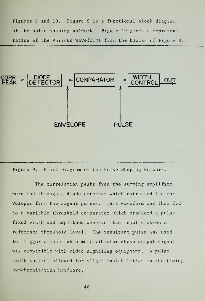
9. Block Diagram of the Pulse Shaping Network 40
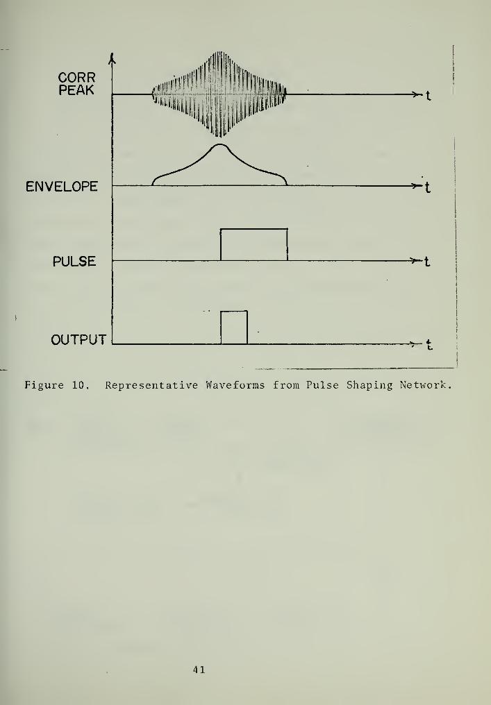
10. Representative Waveforms from Pulse ShapingNetwork 41
11. Transmitter Subsystem Functional Block Diagram 42
12. Receiver Subsystem Functional Block Diagram 43
13. Circuit Diagram of a Typical Active FilterAmplifier - 44
14. Circuit Diagram of a Typical OP -AMP BufferAmplifier - -- 46
15. Circuit Diagram of a Typical OP-AMP SummingAmplifier 47
16. CW Noise Test Setup 50
17. (A) Piezoelectric Crystal, With Transducer 67
(B) Cross Section, Showing Launched Surface Wave 67
18. Surface Wave Device with Launch and ReceiveTransducers 68
19. Phase Coding of the Output Transducers 70
20. Amplitude Coded Waveforms 7 1
21. Bi-Phase Coded Binary Sequence 110 1-- -- ?2
8 •


22. Time Autocorrelation Function of the WaveformShown in Figure 21 73
23. ASWD Modification for Correlation Process 74
24. Summing R.. + RRB to Obtain the Correlation 76
25. ASWD with External Connections 77
26. ASWD Bottom View 78
27. ASWD Transducer Phase Coding - 79
28. ASWD Impulse Response 79
29. Expanded View of ASWD Impulse Response 80
30. Impulse Response Phase Differences 81
31. Autocorrelation Functions 81
32. Sum of Autocorrelation Functions 81


GLOSSARY OF SYMBOLS AND TERMS
Anti-jam
ASWD
BNC
CommunicationSecurity
CW
Data Rate
DB
FH
Golay Comple-mentary Code
HF
Hybrid SSSystem
MatchedFilter
MODEM
PG
PN
RPV
S-Band
SMA
SNR
SpreadSpectrumTechniques
Capability of rejection of jamming signals.
Acoustic Surface Wave Device.
Type connector for coaxial cable.
Message content coding.
Continuous Wave.
Information transmission rate in bits persecond.
Decibel
.
Frequency Hop.
A pair of code sequences with an infinitecorrelation peak-to-peak ambiguity ratiowhen detected with a matched filter.
High Frequency (3MHz - 30MHz)
.
SS system employing two or more differentmethods of spectrum spreading.
Filter whose impulse response is matchedto the signal input.
Modulator/demodulator pair.
Processing Gain.
Pseudo Noise.
Remotely Piloted Vehicle.
2 Gigahertz to 4 Gigahertz Frequency range.
Type connector for coaxial cable.
Signal- to-Noise Ratio.
Processes which cause the bandwidth of a
signal waveform to be deliberately extendedin order to achieve certain transmissionadvantages
.
10

SS - Spread Spectrum.
Transmission - Protection against the disclosure of signalSecurity transmission.
11

ACKNOWLEDGEMENT
S
The writer wishes to express his gratitude to the various
members of the Naval Postgraduate School faculty, staff, and
student body whose assistance and encouragement contributed
to the success of this thesis investigation. Among these are
Professor Stephen Jauregui, Jr. whose guidance and support
made this effort challenging and rewarding.
Thanks are extended to Mr. James Alsup and Mr. Harper
Whitehouse of the Naval Undersea Center, San Diego, California,
who contributed significantly to the understanding of the
acoustic surface wave devices constructed for this thesis.
Thanks are also extended to Mr. James A. Kivett and Mr.
Edward Koist of Hughes Aircraft Company, Ground System
Division, Fullerton, California, for their assistance and
cooperation during my industrial experience tour at their
facility. Participation in the developmental and testing
stages of their WCCM and PLRS spread spectrum systems gave
much insight into and understanding of realizable spread
spectrum systems.
A special thanks is extended to Lt. Laird W. Stanton,
USN, a friend and fellow student, for his tireless assistance
during the testing and evaluation phase of this thesis research
12

I. INTRODUCTION
The companion objectives of reliability, security, and
speed have led to many changes and trade-offs in the con-
cepts and design of military tactical and strategic com-
munications systems. Although modern communications technology
has reached a level of engineering sophistication that af-
fords vast improvements in each of the major objective areas
over our earliest communications networks, these improvements
have been challenged by comparable improvements in signal
jamming and signal interception techniques.
In general, the trade-offs have been attempts to balance
the objective requirements to meet the particular employment
of the communication network. A trade-off in a military
communications system that enhances the attainment of one of
the major objectives while degrading the system's ability to
accomplish another major objective will always suffer since
a hostile party will simply shift its emphasis toward the
new weakness. A system that shows a major improvement in
speed may have bandwidth and channel capacity requirements
that make secure encryption difficult or hostile jamming a
predictable threat.
Not all of the emphasis of the accomplishment of major
objectives has been focused on the larger military communica-
tions systems. There exists many requirements for communica-
tions systems and networks that are small, even man-pack size,
that must attain the same objectives of reliability, security
13

and speed. Here, as in the larger systems, hostile signal
jamming or hostile signal interception of communication sig-
nals can be extremely detrimental to a military operation.
Techniques that have become popular in larger communications
systems such as high power (enhancing reliability) and elab-
orate encryption/decryption schemes (enhancing communication
security) suffer in meeting the cost, size, and power con-
sumption requirements of these smaller systems.
The frequency assignment problem becomes one of prime
concern when the information to be transmitted is video data.
Here the bandwidth before conventional encryption is suffi-
ciently wide that this form of providing security becomes
particularly impractical for general military usage and all
but impossible for compact video systems.
A communication technique that promises simultaneous im-
provements in the reliability, security, and speed of mili-
tary communications systems is spread spectrum communications.
This technique involves the processing of a limited bandwidth
signal of a specified average spectral power density to sub-
stantially increase the bandwidth of the information signal
while decreasing the signal's average spectral power density
over the transmitted bandwidth. This process results in a
transmitted signal that has a negative signal-to-noise ratio
over the increased bandwidth.
Whereas this reduced level of transmitted signal gives
a measure of covertness to the transmission, the real security
of the system comes from the coding involved in the signal
spreading process.
14

System reliability is enhanced because of the inherent
"anti-jam," "multipath rejection," and "interference rejec-
tion" that comes from the bandwidth spreading/compression
scheme used in the communication MODEM.
There are currently three principle methods of spreading
the spectrum of communications signals: pseudo-noise random
code systems, frequency hop systems, and matched filter
techniques, such as acoustic surface wave device (ASWD)
matched filter systems.
In Psuedo-Noise (PN) systems, the information signal is
combined with a noise-like pseudo random code. The resultant
signal is one with a bandwidth that is approximately equal
to that of the pseudo random code which is usually a thousand
or more times as wide as the original information signal.
The receivers of these PN systems must reapply a code iden-
tical to the one at the transmitter to compress the bandwidth
of the transmitted signal and recover the original signal
information. A major consideration in the design and imple-
mentation of PN spread spectrum systems is the maintaining
of PN code synchronization between the transmitter and
receiver.
Frequency Hop systems cause the information signal to
be transmitted at discrete frequencies over a large frequency
band at a random sequence and a rapid rate. The resultant
waveform is one with a bandwidth that"" is equal to the range
of frequencies through which the information signal "hops."
The sequence of frequency transmissions are determined by a
15

pseudo random code in the transmitter. An identical code
in the receiver causes the receiver to track the transmitter
frequencies. As in the PN spread spectrum systems, frequency
hop systems are plagued by the complexity at code synchroni-
zation problems.
Spread spectrum systems employing Acoustic Surface Wave
Devices can avoid the necessity of maintaining PN code syn-
chronization between transmitter and receiver by utilizing
ASWD's in the system MODEM to provide a passive correlator
for signal encoding/decoding and bandwidth expansion/com-
pression. (Refer to Appendix A)
This thesis reports on the design, building, and testing
of a spread spectrum communications system employing com-
plementary coded acoustic surface wave devices.
A. STATEMENT OF THE PROBLEM
Current advances in the development of remotely piloted
vehicles (RPV) have caused these airborne platforms to be
considered by military planners for many uses formerly
relegated to manned aircraft. Long on-station endurance
time, low vulnerability and risk, optimum space utilization,
and multiple launch sites are all factors which lead to the
prediction that suitably equipped RPV's will play significant
roles in future military surveillance operations as well as
strategic plans for tactical offensive weapons exchanges.
Successful employment of these remote platforms require
communications links that provide real-time information in
a reliable, covert manner. The airborne equipment providing
16

the communications link must be small and lightweight to
provide maximum space utilization for sensors and offensive
weapons
.
A particular problem has been that of providing a suit-
able down-link for the video data. Present experimental
systems have either provided neither encoding nor processing
gain for the video information or limited encoding without
processing gain for the real-time video link. A hostile
force would quickly exploit such system inadequacies, pos-
sibly leading to the failure of a critical mission.
The necessity of providing a down-link for real-time
video data that is secure, covert, and reliable, and in a
package that is suitable for tactical RPV employment, was
the driving force for this thesis.
B. DEFINING THE THESIS
The initial consideration was that of determining how
best to attack the problem of providing significant pro-
cessing gain for a signal that already has a bandwidth that
is several megahertz wide. As processing gain (PG) , which
is a measure of the anti-jam of the system, is given by
pr transmitted bandwidthinformation bandwidth '
providing 30db of processing gain to a video signal of 2MHz
bandwidth would require a spread spectrum bandwidth of 2GHz.
State-of-the-art equipments with bandwidths in the gigahertz
range are characterized by bulkiness and high power requirements
The first breakthrough in a practical solution to the
problem was a realization by Dr. Robert W. Means of the Naval
17

Underseas Center, San Diego, that a real-time video pre-
sentation could be provided from video data that has been
reduced to a data rate of approximately 200 kilobits per
second by redundancy reduction. (See Reference 1)
Since this video reproduction is adequate for many
military applications, the objective of this thesis was to
design, build, and test a system which could provide a light-
weight spread spectrum down-link for 200 kilobit data.
1. General Considerations
The problem definition required that any solution
must consist of a system which provides anti-jam rejection
for the video channel. This requirement forced considera-
tion of spread spectrum techniques. Since spread spectrum
techniques involve ideas that are relatively new and equip-
ment and devices that border on the very fringes of the
state-of-the-art, the first consideration was whether this
thesis should be an entirely theoretical investigation, a
survey of current attempts to provide a practical solution,
or an investigation leading to the design, building, and
testing of a candidate solution.
Work done by Cocci in using acoustic surface wave
devices with Golay coding (See Reference 2) to build a spread
spectrum MODEM for voice communications provided encourage-
ment and motivation for the consideration of having this
thesis result in a working product capable of achieving the
desired qualities of an RPV video down-link.
Further considerations led to the realization that
providing a completed system capable of operating in the
18

S-band would not be necessary. In fact, a completed system
with an output frequency centered in, the HF-band would lend
itself better to laboratory testing of the system's anti-jam
capabilities. It was therefore decided that the finished
product should demonstrate all of the aspects of a working
system except operation in the S-band.
2 . Physical Considerations
The constraint that the completed system should in-
clude an RPV transmitter that is size and weight limited
was an obvious one. This requirement of compactness forced
that integrated circuits be considered for maximum utiliza-
tion. In addition to integrated circuits contributing to
space efficiency they promised to be easily adaptable to
the voltage levels expected on board the aircraft. Since
many new concepts required circuits for which integrated
circuits would not be available, these additional circuits
were required to be carefully designed and constructed for
space and power efficiency.
The system was to be designed to operate for long
periods of time, for compatibility with the long endurance
time expected of future RPV's.
An additional physical consideration of primary
concern was that of mutual compatibility. The completed
product was required to be capable of surviving conditions
of extreme temperature changes as well as being able to
operate effectively in a region of dense electro-magnetic
activity.
19


Simplicity was a physical constraint that was forced
by the other physical requirements. The direct approach
usually resulting in fewer components and hence a more re-
liable system.
Cost being a factor, off-the-shelf parts were sought
for their economy as well as their proven dependability, but
when off-the-shelf items could not be provided with the
requisite size and minimum power requirements, other options
were dictated. So the overriding physical consideration
was that of compactness followed by simplicity, cost economy,
and power efficiency.
3. Theoretical Considerations
The requirement that the down- link for video data
be covert and have anti-jam rejection meant that any ac-
ceptable system would require processing to spread the
spectrum of the video information signal bandwidth. Since
an assumption of covertness alone is not sufficient to
guarantee adequate security, some type of information en-
coding had to be provided for as well. Theoretically the
signal encoding could be obtained by the same mechanism that
spread the spectrum of the signal. This method of approach
was to be pursued where practicality and consistency with
physical constraints permitted.
Although a reduction of the video data rate to 200
kilobits per second represented a significant decrease in
the video signal bandwidth, providing high processing gain
by band spreading alone would still require a spread spectrum
bandwidth of several hundred megahertz. Theoretically,
20

processing gain could be increased over that predicted by
the spread spectrum signal bandwidth to information signal
bandwidth ratio if additional processing gain can be pro-
vided from the coding/decoding method. (See Reference 3
and Appendix B.)
Since the ASWD matched filters reported on in
Reference 2 and described in Appendix A were available and
since they had demonstrated the possibility of providing a
spread spectrum signal by using Golay complementary coded
devices, it was decided that these units should be given
every consideration as candidates for inclusion in the final
product.
It was also decided that if these devices were used
in the final product that comprehensive testing should be
performed to determine if the method of coding did in fact
contribute to the processing gain of the system.
Section II gives a detailed discussion of the system
specifications. Sections III and IV address the design and
construction portion of the thesis project with major empha-
sis on why one method of approach was chosen in preference
to another. Section V is a description of the testing pro-
cedure of the completed product, and Section VI reports on
the results of testing the system. Section VII summarizes
the thesis effort. Appendices are provided that supplement
and illuminate the main text.
21

II. DESIGN SPECIFICATIONS AND OBJECTIVES
The overall objective of the system design was to pro-
vide a secure, covert communications link for the transmis-
sion of reduced video data from a remotely piloted vehicle
(RPV) to a surface based command center.
Since the system transmitter was to be part of the pay-
load of a weight and power limited RPV, it was required
that the transmitter be as light as possible (with a goal
of one pound exclusive of power supply) and have a minimum
power budget commensurate with range requirements.
The system was to be capable of surviving a maximum
doppler rate of 50 Kts , and to be capable of communi cat ions
at a maximum of 100 nautical miles.
At a reduced video data rate of 200 kilobits per second,
the system was designed to provide a minimum of 20db of
anti-jam with a goal of 25 to 30db of anti-jam.
The system was to employ spread spectrum techniques
utilizing an acoustic surface wave device modem for signal
bandwidth expansion/compression and data encoding/decoding.
Although the system is expected to be operated in the
S-band, the model designed, built, and tested for this thesis
study was designed to operate in the HF band to facilitate
laboratory testing; conversion of the system to S-band
operation being a trivial extension of the thesis design.
In addition to the transmitter of the system having a
weight specification of approximately one pound, both the
22

transmitter and receiver were required to be compact in
order to economize on space and to facilitate portability.
And although no specific restrictions were imposed on the
receiver size, the receiver was to be made as small as the
state-of-the-art would permit commensurate with transmitter
size specifications.
Although the system was not required to provide a power
supply for the RPV transmitter, the transmitter was required
to be operable using standard aircraft voltage levels.
All components were required to be shielded in such a
manner to permit satisfactory operation in an environment
of high electro-magnetic activity and to be constructed
using engineering practices that would minimize spurious
radiations
.
Test points were to be provided where necessary to per-
mit testing of the system's performance in various noise
and interference environments.
23

III. SYSTEM DESIGN AND FABRICATION
Consistent with the size and weight specifications de-
fined in the earlier sections of this thesis, every con-
sideration was given to space and weight economy in the
design phase of this effort. The first major space saving
option occurred in the consideration of a system waveform.
Whereas other system specifications had already imposed the
requirement of a spread spectrum waveform, the many candi-
date methods of providing spread spectrum modulation, as
listed in Section I , left the choice of a particular spread
spectrum waveform a significant option of consideration.
Since the choice of a spread spectrum waveform dictates
much of the rest of the system design, the features of the
various methods of providing spread spectrum modulation
which led to the final choice will be discussed in detail.
A. CHOICE OF SPREAD SPECTRUM MODULATION SCHEME
Four candidate methods of providing a spread spectrum
waveform were considered. These included pseudo noise (PN)
code modulation, frequency hop (FH) modulation, a hybrid
combination of PN code modulation with frequency hopping,
and modulation by acoustic surface wave device. Detailed
discussions of these methods of spread spectrum modulation
are included in References 2 and 5. Only the salient fea-
tures of each method will be discussed here in relation to
the impact of these features on the final design choice.
24

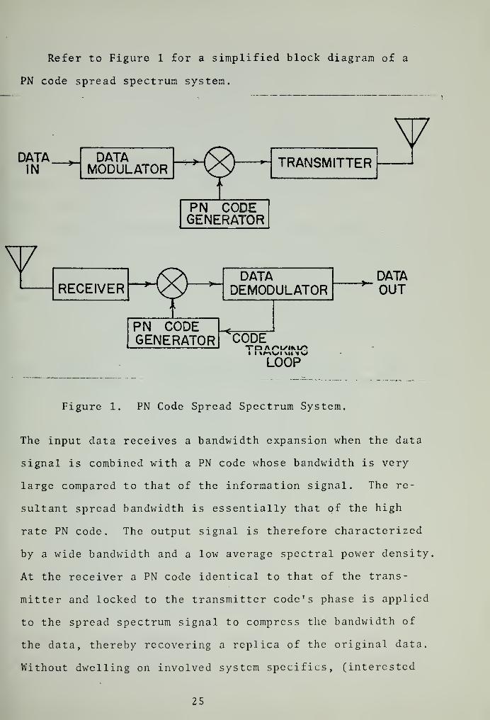
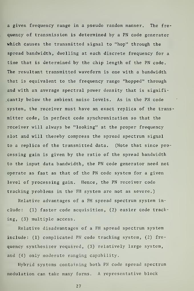
Refer to Figure 1 for a simplified block diagram of a
PN code spread spectrum system.
DATAIN
v
DATAMODULATOR
RECEIVER
TRANSMITTER
PN CODEGENERATOR
DATADEMODULATOR
PN CODEGENERATOR CODE
LOOP
v
DATA^"OUT
Figure 1. PN Code Spread Spectrum System.
The input data receives a bandwidth expansion when the data
signal is combined with a PN code whose bandwidth is very
large compared to that of the information signal. The re-
sultant spread bandwidth is essentially that of the high
rate PN code. The output signal is therefore characterized
by a wide bandwidth and a low average spectral power density.
At the receiver a PN code identical to that of the trans-
mitter and locked to the transmitter code's phase is applied
to the spread spectrum signal to compress the bandwidth of
the data, thereby recovering a replica of the original data.
Without dwelling on involved system specifics, (interested
25

readers should refer to Reference 5) the advantages and
disadvantages of a PN code system with respect to its use
in the final design will be listed. .• Features common to all
candidate systems will be omitted.
Relative advantages of a PN code spread spectrum system
include: (1) accurate ranging, (2) superior communications
security capability, (3) multiple access, and (4) multi-
path rejection.
Relative disadvantages of a PN code spread spectrum sys-
tem include: ' (1) slow code acquisition in the receiver,
(2) complicated PN code tracking system, and (3) sophisti-
cated (space consuming) PN code generator required.
Refer to Figure 2 for a simplified block diagram of a
FH spread spectrum system.
ADATAIN-
DATAMODULATOR
FREQUENCYSELECTOR L
T>~ TRANSMITTER
PN CODEGENERATOR
AMIXER
H3
DATADEMODULATOR
DATAOUT
FREQUENCYSELECTOR
PN CODEGENERATOR
Figure 2. FH Spread Spectrum System.
In the FH method of providing a spread spectrum waveform, the
data signal is transmitted at various frequencies throughout
26

a given frequency range in a pseudo random manner. The fre-
quency of transmission is determined by a PN code generator
which causes the transmitted signal to "hop" through the
spread bandwidth, dwelling at each discrete frequency for a
time that is determined by the chip length of the PN code.
The resultant transmitted waveform is one with a bandwidth
that is equivalent to the frequency range "hopped" through
and with an average spectral power density that is signifi-
cantly below the ambient noise levels. As in the PN code
system, the receiver must have an exact replica of the trans
mitter code, in perfect code synchronization so that the
receiver will always be "looking" at the proper frequency
slot and will thereby compress the spread spectrum signal
to a replica of the transmitted data. (Note that since pro-
cessing gain is given by the ratio of the spread bandwidth
to the input data bandwidth, the PN code generator need not
operate as fast as that of the PN code system for a given
level of processing gain. Hence, the PN receiver code
tracking problems in the FH system are not as severe.)
Relative advantages of a FH spread spectrum system in-
clude: (1) faster code acquisition, (2) easier code track-
ing, (3) multiple access.
Relative disadvantages of a FH spread spectrum system
include: (1) complicated PN code tracking system, (2) fre-
quency synthesizer required, (3) relatively large system,
and (4) only moderate ranging capability.
Hybrid systems containing both PN code spread spectrum
modulation can take many forms. A representative block
27

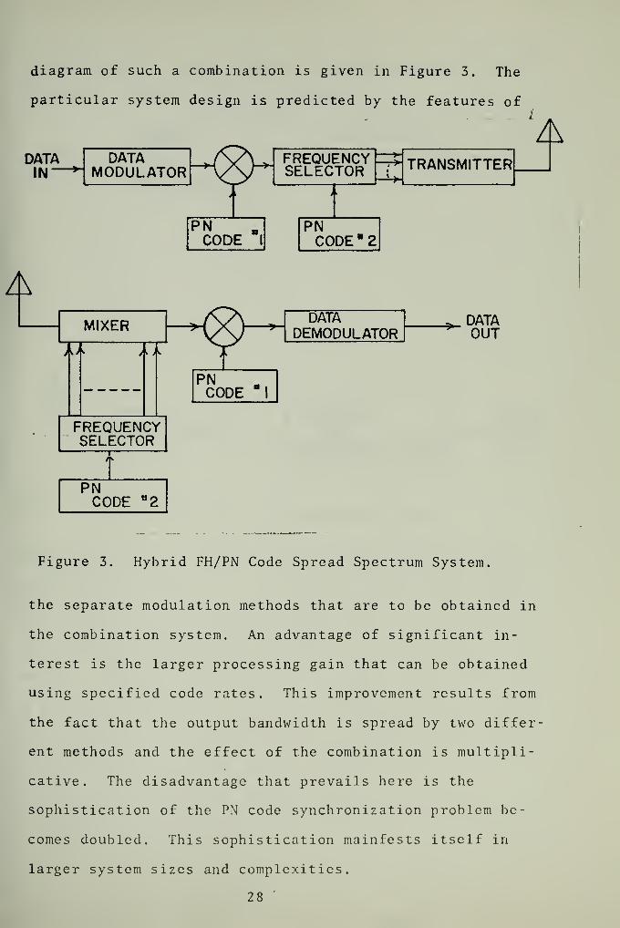
diagram of such a combination is given in Figure 3. The
particular system design is predicted by the features of
ADATAIN—
*
DATAMODULATOR
FREQUENCYSELECTOR
FREQUENCYSELECTOR
—j—
PNCODE d 2
-r> TRANSMITTER
PNCODE "
2
DATADEMODULATOR
DATAOUT
Figure 3. Hybrid FH/PN Code Spread Spectrum System.
the separate modulation methods that are to be obtained in
the combination system. An advantage of significant in-
terest is the larger processing gain that can be obtained
using specified code rates. This improvement results from
the fact that the output bandwidth is spread by two differ-
ent methods and the effect of the combination is multipli-
cative. The disadvantage that prevails here is the
sophistication of the PN code synchronization problem be-
comes doubled. This sophistication mainfests itself in
larger system sizes and complexities.
28

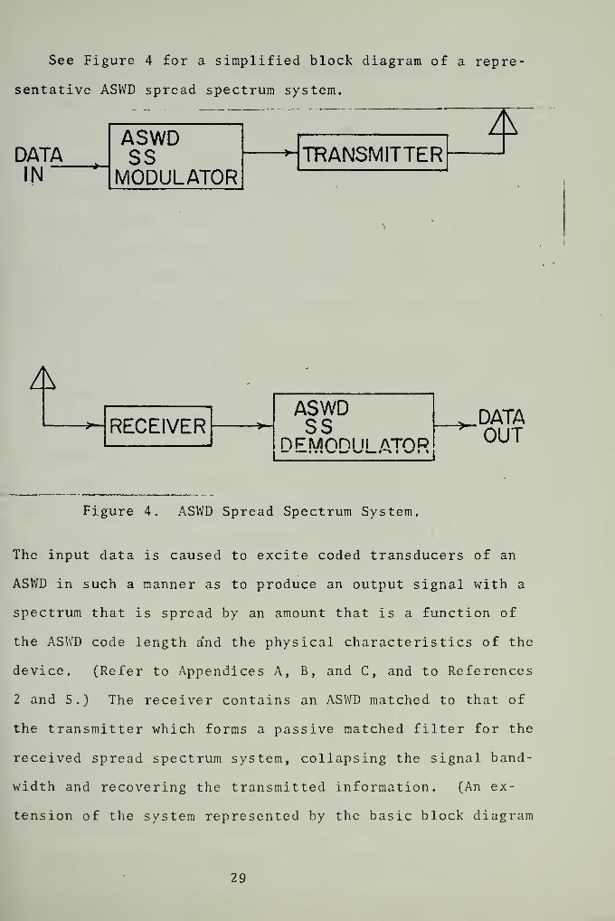
See Figure 4 for a simplified block diagram of a repre
sentative ASWD spread spectrum system.
DATAASWDSS
MODULATORTRANSMITTER
A
ARECEIVER
ASWDSS
nFMOni II ATOPDATAOUT
Figure 4. ASWD Spread Spectrum System.
The input data is caused to excite coded transducers of an
ASWD in such a manner as to produce an output signal with a
spectrum that is spread by an amount that is a function of
the ASWD code length a'nd the physical characteristics of the
device. (Refer to Appendices A, B, and C, and to References
2 and 5.) The receiver contains an ASWD matched to that of
the transmitter which forms a passive matched filter for the
received spread spectrum system, collapsing the signal band-
width and recovering the transmitted information. (An ex-
tension of the system represented by the basic block diagram
29

of Figure 4 includes systems containing multiple devices,
such as the ones reported on in Reference 2 and in this
thesis.) Of noteworthy interest is the fact that the system
of Figure 4 does not contain a PN code generator. This
significant advantage in simplicity is not without a price
as will be seen in later discussion.
Relative advantages of ASWD systems include: (1) sim-
plicity, (2) insensitivity to doppler, (3) reduced code
synchronization problems, (4) comparative small size, and
(5) passive matched filter.
Relative disadvantages of ASWD systems include: (1)
low communication security, (2) limited processing gain
available, (3) no ranging capability, and (4) unproven
technique
.
Along with advantages and disadvantages of the candi-
date systems that resulted from natural properties and
characteristics of the components of the various systems,
another important aspect of the individual systems had to
be considered. The factor alluded to was the availability
of critical system components. Since this thesis effort
was to result in a product capable of being laboratory
tested, due concern was warranted for the availability of
devices and parts necessary to complete the chosen type of
system early enough for testing to be completed within the
time allowed for the thesis research.
After consideration of the advantages and disadvantages
of the candidate spread spectrum methods, the apparent ideal
choice was that of a hybrid system containing a PN code
30

spread spectrum waveform that "hops" through a block of
frequencies at a rate determined by a." different PN code
pattern. This arrangement would permit maximum processing
gain with communication security as well as transmission
security. However, system complexity, projected system
size, and the fact that critical system components were not
available forced the rejection of this hybrid proposal. A
similar argument forced a rejection of the apparent second
choice which was to use a spread spectrum waveform generated
by the PN code method. Mr. James A. Kivett and other en-
gineers at the Hughes Aircraft Company, Ground Systems
Division, Fullerton, California, were extremely helpful in
many discussions of the availability of the companion com-
ponents of the candidate systems.
The next choice, and the ultimate one, was that of
using an ASWD waveform for the spread spectrum modulation.
Although this choice was largely dictated by the fact that
two Golay complementary coded pairs of ASWD matched filters
were available, this choice did not represent an unacceptable
concession. Aside from the advantages listed in earlier
paragraphs, providing the spread spectrum waveform via
Golay coded ASWD pairs promised interesting features for
investigation. One such feature for investigation was the
expectation that the Golay coding would produce a measure
of processing gain greater than that predicted by a simple
comparison of the information bandwidth with the spread
spectrum bandwidth. These advantages and special features
along with the opportunity of working with a device that
31

bordered on the very fringe of the state-of-the-art pro-
vided special stimulus for the design work of this thesis.
B. ELEMENTS OF DESIGN
The choice of the Golay coded ASWD's as sources of the
spread spectrum waveform imposed a requirement that the
transmitter/receiver combination include some form of
multiplexing. Two separate channels of spread spectrum
information result from the complementary coding. A second
design problem was that of modulating the ASWD pair with a
data rate of approximately 200 kilobits per second. The
devices had already been successfully utilized in a voice
MODEM, (see Reference 2) , but certain modifications to the
modulation scheme would be necessary to make the devices
compatible with this higher rate of information transmis-
sion. Other design problems included amplification and
transmission of the multiplexed signal, reception and am-
plification of the radiated signal, demultiplexing and
demodulation of the received signal, and system integration
for space economy and transmission efficiency.
So the design problem can be divided into the following
elements: (1) modulating the ASWD's, (2) multiplexing the
complementary waveforms, (5) amplification and transmission
of the multiplexed signal, (4) reception and amplification
of the spread spectrum signal, (5) demultiplexing and de-
modulating the received signal, and (6) system integration.
Each element will be discussed only in regard to its
impact on the final product. Specific circuitry will be
discussed only when the approach is significantly different
32

from normal practice, or when a cause and effect relation-
ship is not obvious. The system integration will be covered
in a separate section.
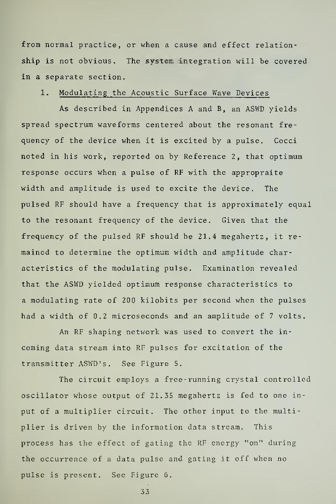
1. Modulating the Acoustic Surface Wave Devices
As described in Appendices A and B, an ASWD yields
spread spectrum waveforms centered about the resonant fre-
quency of the device when it is excited by a pulse. Cocci
noted in his work, reported on by Reference 2, that optimum
response occurs when a pulse of RF with the appropraite
width and amplitude is used to excite the device. The
pulsed RF should have a frequency that is approximately equal
to the resonant frequency of the device. Given that the
frequency of the pulsed RF should be 21.4 megahertz, it re-
mained to determine the optimum width and amplitude char-
acteristics of the modulating pulse. Examination revealed
that the ASWD yielded optimum response characteristics to
a modulating rate of 200 kilobits per second when the pulses
had a width of 0.2 microseconds and an amplitude of 7 volts.
An RF shaping network was used to convert the in-
coming data stream into RF pulses for excitation of the
transmitter ASWD ' s . See Figure 5.
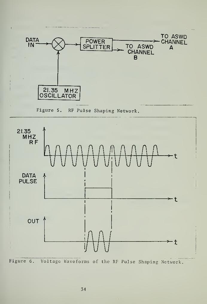
The circuit employs a free-running crystal controlled
oscillator whose output of 21.35 megahertz is fed to one in-
put of a multiplier circuit. The other input to the multi-
plier is driven by the information data stream. This
process has the effect of gating the RF energy "on" during
the occurrence of a data pulse and gating it off when no
pulse is present. See Figure 6.
33

DATAIN- POWER
SPLITTER
TO ASWD-*- CHANNEL
TO ASWD ACHANNELB
21.35 MHZOSCILLATOR
Figure 5. RF Pulse Shaping Network,
21.35MHZRF
DATAPULSE
OUT
Figure 6. Voltage Waveforms of the RF Pulse Shaping Network
34


(Notice, in Figure 6, that the pulse width is controlled by
the width of the input data pulses.) The pulsed RF signal
is fed to a power splitter to provide two identical outputs,
which are necessary for driving the complementary coded
ASWD's simultaneously.
2 . Multiplexing the Complementary Waveforms
The output of the ASWD's after proper excitation
consisted of two spread spectrum signals each with a center
frequency of approximately 21.4 megahertz and a bandwidth
of approximately four megahertz. Multiplexing of the two
channels was performed by translating one of the channels
to a center frequency of 30 megahertz. This 8.6 megahertz
separation of the channels afforded a guard band that per-
mitted adequate channel separation without the necessity of
complicated space consuming filters. See Figure 7.
RF PULSES
TRANSMITTERASWD's
RF PULSES
SUMMINGAMPLIFIER ^OUT
8.6 MHZOSCILLATOR
Figure 7. Frequency Multiplexer,
35

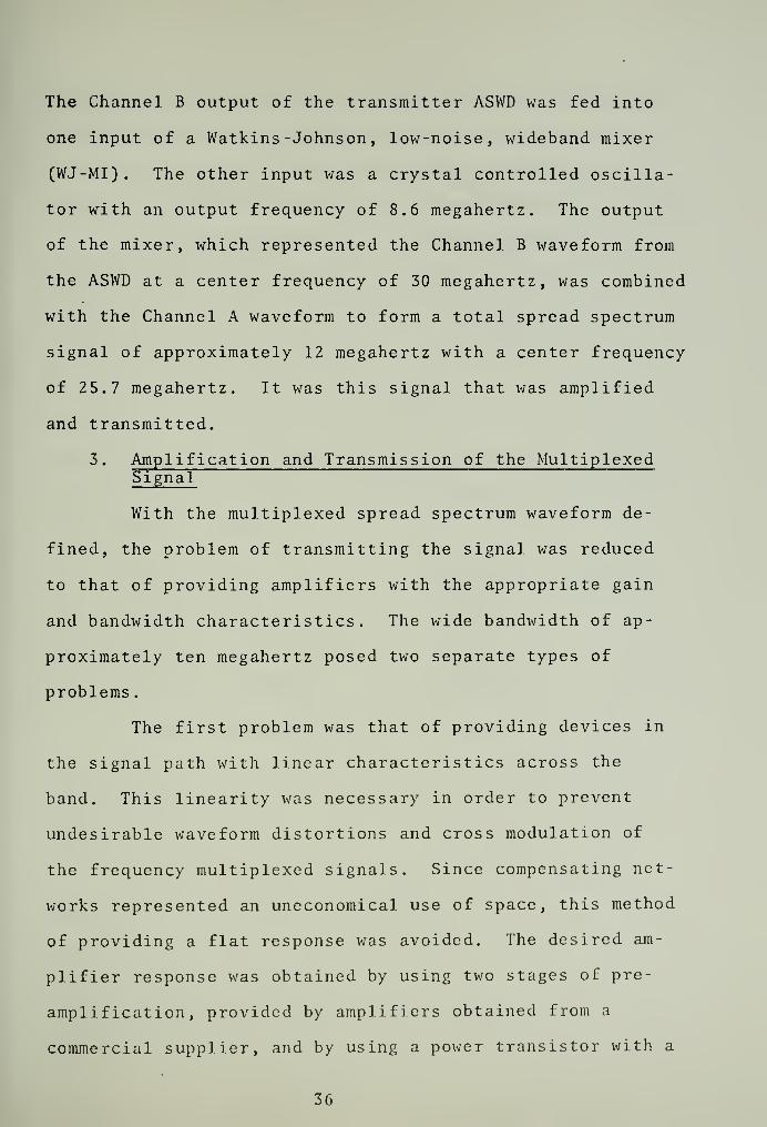
The Channel B output of the transmitter ASWD was fed into
one input of a Watkins -Johnson, low-noise, wideband mixer
(WJ-MI) . The other input was a crystal controlled oscilla-
tor with an output frequency of 8.6 megahertz. The output
of the mixer, which represented the Channel B waveform from
the ASWD at a center frequency of 30 megahertz, was combined
with the Channel A waveform to form a total spread spectrum
signal of approximately 12 megahertz with a center frequency
of 25.7 megahertz. It was this signal that was amplified
and transmitted.
3. Amplification and Transmission of the MultiplexedSignal
With the multiplexed spread spectrum waveform de-
fined, the problem of transmitting the signal was reduced
to that of providing amplifiers with the appropriate gain
and bandwidth characteristics. The wide bandwidth of ap-
proximately ten megahertz posed two separate types of
problems.
The first problem was that of providing devices in
the signal path with linear characteristics across the
band. This linearity was necessary in order to prevent
undesirable waveform distortions and cross modulation of
the frequency multiplexed signals. Since compensating net-
works represented an uneconomical use of space, this method
of providing a flat response was avoided. The desired am-
plifier response was obtained by using two stages of pre-
amplif ication,provided by amplifiers obtained from a
commercial supplier, and by using a power transistor with a
36

high gain bandwidth product. Features of the commercially
available amplifiers included small size (approximately
1.5 oz) 30 decibels of power gain, flat response from 0.5
megahertz to 100 megahertz, and a three decibel noise figure
The second problem that resulted directly from the
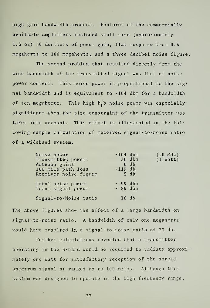
wide bandwidth of the transmitted signal was that of noise
power content. This noise power is proportional to the sig-
nal bandwidth and is equivalent to -104 dbm for a bandwidth
of ten megahertz. This high k b noise power was especially
significant when the size constraint of the transmitter was
taken into account. This effect is illustrated in the fol-
lowing sample calculation of received signal-to-noise ratio
of a wideband system.
Noise powerTransmitted power:Antenna gains100 mile path lossReceiver noise figure
Total noise powerTotal signal power
Signal-to-Noise ratio
104 dbm30 dbm
db119 db
5 db
99 dbm89 dbm
10 db
(10 MHz)(1 Watt)
The above figures show the effect of a large bandwidth on
signal-to-noise ratio. A bandwidth of only one megahertz
would have resulted in a signal-to-noise ratio of 20 db
.
Further calculations revealed that a transmitter
operating in the S-band would be required to radiate approxi
mately one watt for satisfactory reception of the spread
spectrum signal at ranges up to 100 miles. Although this
system was designed to operate in the high frequency range,
37

for ease of testing, the transmitted power was designed to
be between one and two watts.
4. Reception and Amplification of the Spread SpectrumSignal
The problem of receiving and amplifying the spread
spectrum signal was much like that of amplifying the signal
in the transmitter. The wide bandwidth caused the major
emphasis of the receiver to be on signal linearity and low
noise susceptibility. The input stages of the receiver were
designed around a commercially available wideband amplifier
with a noise figure of three decibels and a power gain of
30 db . This low noise input amplifier caused the overall
noise figure of the input amplifiers to be approximately
four decibels. Subsequent amplifiers in the signal path of
the receiver were required as interface elements between
the various receiver functional devices. These amplifiers
are described in detail in the following section on system
integration.
5
.
Demultiplexing and Demodulating the Received Signal
The two channels of the spread spectrum were sepa-
rated by active filters in the receiver signal path. See
Figure 8.
The filter of Figure 8 labeled filter A was designed
and built to have four megahertz bandwidth with a center
frequency of 30 megahertz. The output of this filter was
mixed with a local oscillator frequency of 8.6 megahertz to
provide a difference frequency of 21.4 megahertz and a band-
width of four megahertz. The filter of Figure 8 labeled
38

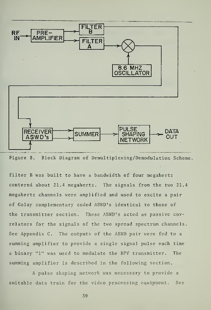
RFIN"
PRE-AMPLIFIER
FILTERB
FILTERA
8.6 MHZOSCILLATOR
1RECEIVERASWD's SUMMER
PULSESHAPINGNETWORK
DATAOUT
Figure 8. Block Diagram of Demultiplexing/Demodulation Scheme
filter B was built to have a bandwidth of four megahertz
centered about 21.4 megahertz. The signals from the two 21.4
megahertz channels were amplified and used to excite a pair
of Golay complementary coded ASWD's identical to those of
the transmitter section. These ASWD's acted as passive cor-
relators for the signals of the two spread spectrum channels.
See Appendix C. The outputs of the ASWD pair were fed to a
summing amplifier to provide a single signal pulse each time
a binary "1" was used to modulate the RPV transmitter. The
summing amplifier is described in the following section.
A pulse shaping network was necessary to provide a
suitable data train for the video processing equipment. See
39

Figures 9 and 10. Figure 9 is a functional block diagram
of the pulse shaping network. Figure 10 gives a represen-
tation of the various waveforms from the blocks of Figure 9
CORRPEAK"
DIODEDETECTOR COMPARATOR
ENVELOPE
WIDTHCONTROL OUT
>-
PULSE
Figure 9. Block Diagram of the Pulse Shaping Network.
The correlation peaks from the summing amplifier
were fed through a diode detector which extracted the en-
velopes from the signal pulses. This waveform was then fed
to a variable threshold comparator which produced a pulse
fixed width and amplitude whenever the input crossed a
reference threshold level. The resultant pulse was used
to trigger a monostable multivibrator whose output signal
was compatible with video signaling equipment. A pulse
width control allowed for slight instabilities in the timing
synchronization hardware.
40

CORRPEAK
ENVELOPE
PULSE
OUTPUT
Figure 10. Representative Waveforms from Pulse Shaping Network
41

IV. SYSTEM INTEGRATION
The circuits and devices described in the previous sec-
tion required certain interfaces for consolidation of the
independent elements into an integrated system. In many
instances these interfaces consisted of simple BNC or SMA
connectors. Other simple interfaces included direct wiring
and coupling capacitors. But in most interface situations,
buffer amplifiers, pre-amplifiers , summing amplifiers, or
filters are necessary to make the output of a device com-
patible with the input requirements of the following device
This section describes the various interfaces used to sup-
plement the circuits and devices described in the previous
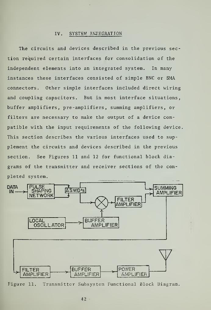
section. See Figures 11 and 12 for functional block dia-
grams of the transmitter and receiver sections of the com-
pleted system.
DATAIN >
PULSESHAPINGNETWORK
ASWD's
FILTERAMPLIFIER
SUMMINGAMPLIFIER
LOCALOSCILLATOR
BUFFERAMPLIFIER
VFILTERAMPLIFIER
BUFFERAMPLIFIER
POWERAMPLIFIER
Figure 11. Transmitter Subsystem Functional Block Diagram.
42

LOCALOSCILLATOR
BUFFERAMPLIFIER
ir
INPUTAMPLIFIER
FILTERAMPLIFIER
FILTERAMPLIFIER
DRIVERAMPLIFIER
DRIVERAMPLIFIER
AS WD 'sSUMMINGAMPLIFIER
PULSESHAPINGNETWORK
DATA"^OUT
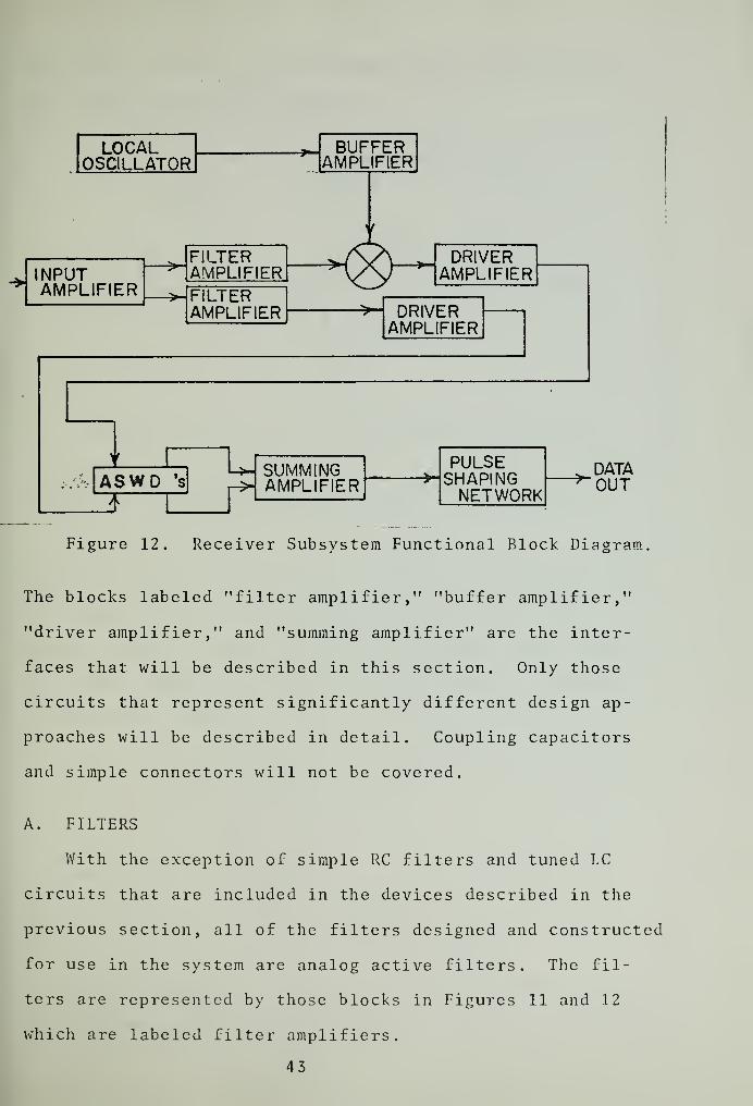
Figure 12. Receiver Subsystem Functional Block Diagram.
The blocks labeled "filter amplifier," "buffer amplifier,"
"driver amplifier," and "summing amplifier" are the inter-
faces that will be described in this section. Only those
circuits that represent significantly different design ap-
proaches will be described in detail. Coupling capacitors
and simple connectors will not be covered.
A. FILTERS
With the exception of simple RC filters and tuned LC
circuits that are included in the devices described in the
previous section, all of the filters designed and constructed
for use in the system are analog active filters. The fil-
ters are represented by those blocks in Figures 11 and 12
which are labeled filter amplifiers.
43

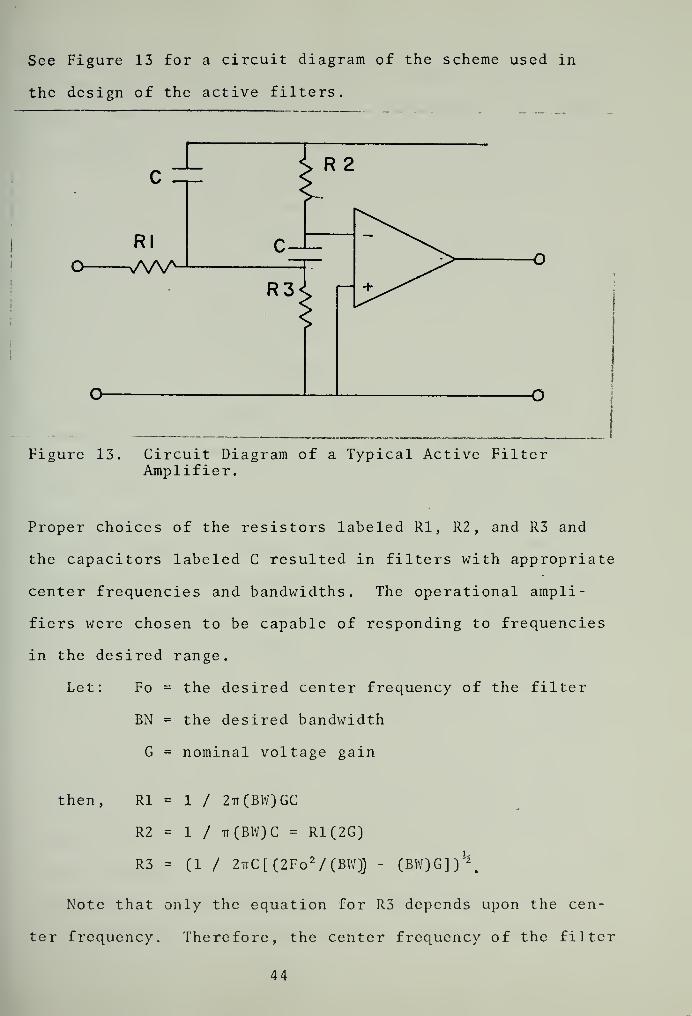
See Figure 13 for a circuit diagram of the scheme used in
the design of the active filters.
Figure 13. Circuit Diagram of a Typical Active FilterAmplifier.
Proper choices of the resistors labeled Rl, R2 , and R3 and
the capacitors labeled C resulted in filters with appropriate
center frequencies and bandwidths. The operational ampli-
fiers were chosen to be capable of responding to frequencies
in the desired range.
Let: Fo = the desired center frequency of the filter
BN = the desired bandwidth
G = nominal voltage gain
then, Rl = 1 / 2tt(BW)GC
R2 = 1 / tt(BW)C = R1(2G)
R3 = (1 / 2ttC[(2Fo 2/(BWJ) - (BW)G])
1
^
Note that only the equation for R3 depends upon the cen-
ter frequency. Therefore, the center frequency of the filter
44

can be adjusted without altering the bandwidth of the filter,
Typical values for a representative filter used in the sys-
tem follows:
Fo = 30MHz
BW = 4MHz
G = lOdb
Rl = 408ft
R2 = 8160ft
R3 = 9.4ft
C - lOpfd.
B. AMPLIFIER INTERFACES
Amplifiers were required to make the outputs of some
stages compatible with the inputs of the following stages.
These interfaces are represented by those blocks of Figures
11 and 12 which are labeled "buffer amplifier," "summing
amplifier," and "driver amplifier." The driver amplifiers
were purchased from a commercial supplier. Features of
these commercially available amplifiers include a three
decibel noise figure, 30 decibels of power gain, BNC con-
nectors, and small physical size (approximately 1.5 ounces).
The other amplifiers were designed and built utilizing in-
tegrated circuit operational amplifiers with high gain
bandwidth products and low noise characteristics. These
amplifiers were designed using standard operational ampli-
fier configurations. All of the IC chips used were readily
available off-the-shelf items. Circular chips were used
in preference to rectangular chips for circuit compactness.
4 5

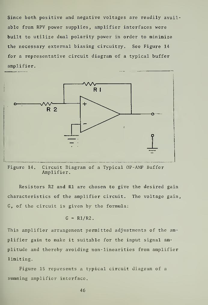
Since both positive and negative voltages are readily avail
able from RPV power supplies, amplifier interfaces were
built to utilize dual polarity power in order to minimize
the necessary external biasing circuitry. See Figure 14
for a representative circuit diagram of a typical buffer
amplifier.
AAAr
Figure 14. Circuit Diagram of a Typical OP-AMP BufferAmplifier.
Resistors R2 and Rl are chosen to give the desired gain
characteristics of the amplifier circuit. The voltage gain,
G, of the circuit is given by the formula:
G = R1/R2.
This amplifier arrangement permitted adjustments of the am-
plifier gain to make it suitable for the input signal am-
plitude and thereby avoiding non-linearities from amplifier
limiting.
Figure 15 represents a typical circuit diagram of a
summing amplifier interface.
46

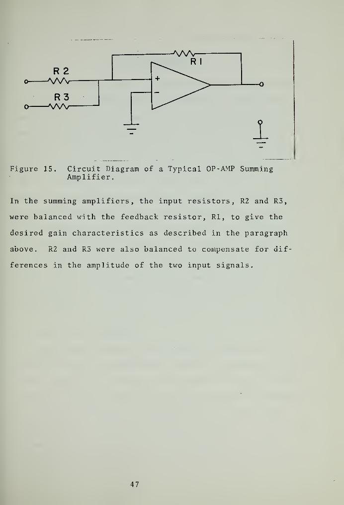
AAAr
iFigure 15. Circuit Diagram of a Typical OP-AMP Summing
Amplifier.
In the summing amplifiers, the input resistors, R2 and R3,
were balanced with the feedback resistor, Rl , to give the
desired gain characteristics as described in the paragraph
above. R2 and R3 were also balanced to compensate for dif-
ferences in the amplitude of the two input signals.
47

V. TEST PROCEDURES.
System and subsystem testings were routinely performed
as components were designed and fabricated. This testing
was necessary to determine circuit waveform parameters so
that the proper interfaces could be provided between the
elements of the system. Whereas most of this testing repre-
sented standard engineering practices, and therefore will
not be described in detail, significantly different pro-
cedures had to be utilized for the testing of the equipment's
anti-jam capabilities. This section describes tests made
on the communication system to determine its performance in
interfering noise environments. The system was tested in
the presence of two types of noise interference that are
often encountered in communications jamming -- narrow band
interference (or continuous wave (CW) ) and wideband noise
interference
.
A. TESTING CONSIDERATION
For an understanding of the effect of processing gain
(PG) on a system's performance, consider a system that will
permit satisfactory receiver output when the received wave-
form has a signal-to-noise ratio of ten decibels or greater
but does not produce an acceptable output when the input
signal-to-noise ratio is less than ten decibels. A reali-
zation of ten decibels of PG in this system would permit
satisfactory operation at a signal-to-noise ratio of unity
48

(0 db) , and a realization of 20 decibels of PG would give
the system the capability of satisfactory performance when
the signal-to-noise ratio was a negative ten decibels. It
is this feature of being capable of recovering a signal
that is well below the level of intentional and incidental
noises that provides the motivation for achieving maximum
processing gain. The level of processing gain provided by
an efficient system can be predicted by dividing the spread
spectrum bandwidth by the bandwidth of the information sig-
nal. Since it was expected that the addition of Golay com-
plementary coding would increase the amount of processing
gain, a major consideration of the testing procedure was
the determination of the effect of this coding on the sys-
tem's processing gain.
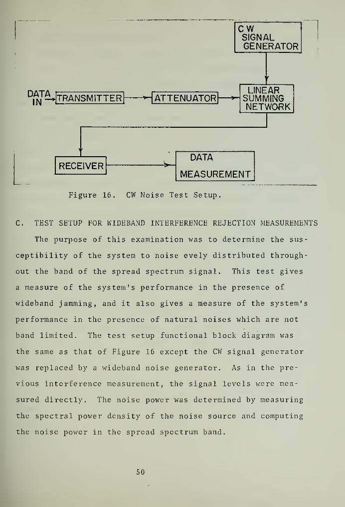
B. TEST SETUP FOR NARROW BAND NOISE REJECTION MEASUREMENTS
The purpose of this examination was to determine not
only the CW interference noise levels that the system could
survive but also the frequency of narrow band interference
that proved most troublesome. This test required accurate
measurements of the signal and noise levels at the receiver
input. See Figure 16 for a functional block diagram of the
CW noise test setup.
This test arrangement permitted direct monitoring of the
input signal-to-noise level by a wideband RF power meter.
The frequency of the CW signal generator could be varied
manually through the band of the spread spectrum waveform
for a determination of the effect of frequency positioning
on the system's performance.
49

cwSIGNALGENERATOR
DATAIN
-4 TRANSMITTER ATTENUATORLINEARSUMMINGNETWORK
RECEIVERDATA
MEASUREMENT
Figure 16. CW Noise Test Setup.
C. TEST SETUP FOR WIDEBAND INTERFERENCE REJECTION MEASUREMENTS
The purpose of this examination was to determine the sus-
ceptibility of the system to noise evely distributed through-
out the band of the spread spectrum signal. This test gives
a measure of the system's performance in the presence of
wideband jamming, and it also gives a measure of the system's
performance in the presence of natural noises which are not
band limited. The test setup functional block diagram was
the same as that of Figure 16 except the CW signal generator
was replaced by a wideband noise generator. As in the pre-
vious interference measurement, the signal levels were mea-
sured directly. The noise power was determined by measuring
the spectral power density of the noise source and computing
the noise power in the spread spectrum band.
50

D. TEST EQUIPMENT AND DEVICES
Attempts were made to provide test conditions that were
as realistic as could be realized in a laboratory test sit-
uation. However, an exact determination of the system's
performance in various noise environment required accurate
measurements of the test parameters. For this reason, sig-
nal and noise power measurements were made with a Hewlett
Packard 232A wideband power meter instead of using a spectrum
analyzer to determine relative signal-to-noise power ratios.
Measurements were made at the inputs of the summing junction
so that the resultant signal-to-noise ratios would be rela-
tively independent of coxial transmission losses.
The CW noise interference signals were provided by an
SG-85, URM-25D signal generator. Signal linearity and sig-
nal frequencies were verified by TEXTRONIX 422 oscilloscope
measurements before injection into the receiver summing
junction.
The wideband noise interference was provided by an
ELGENCO Gaussian noise generator and by using a Watkins-
Johnson Relcom mixer and a URM-25D signal generator for
frequency translation.
Message quality measurements were made using a TSI USM
245A frequency counter. The transmitted data count was
compared with the received data count as described in the
following section to give a measure of transmission reli-
ability in the presence of interfering noises.
51

VI . SYSTEM PERFORMANCE '
This section reports on the results of the tests described
in the previous section. Tests were conducted on the system
to determine the effects of CW and wideband noise interference
on system reliability. These test results give a measure of
the anti-jam capability of the system as well as the ability
of system to survive interference from natural and incidental
noises
.
The test results are tabulated in a manner to show the
relationship between interference noise power levels and
system reliability. Separate tables show the effect of CW
interference frequency positioning. Each table is labeled
according to the condition that prevailed during the test.
The first column of each table gives the total spread
spectrum signal power delivered to the receiver input. Column
two gives the total noise power delivered to the receiver in-
put that is within the passband of the receiver. Columns
one and two are expressed in dbm. Column three gives the
signal-to-noise ratio at the receiver input, expressed in
db . Column four gives the percentage of the messages sent
that were actually received during a particular sample in-
terval. The sample interval chosen for the test was one
second.
During testing for transmission reliability, two types
of error can be expected to occur:
52

FALSE ALARMS A message is received, butno valid message was sent.
MISSED MESSAGE---A valid message was sent,but no message was received.
The tests conducted on this system were designed so that
the probability that a false alarm type error was small
enough to be neglected. This condition was assured by ad-
justing interfering noise levels to be sufficiently low
that the probability of a noise spike would exceed the
receiver threshold level was negligible. So only missed
messages had to be considered in a determination of system
reliability. Messages were transmitted at data rates as
specified on the individual tables, and a count was made
of the valid messages actually received. The ratio of
received messages to transmitted messages times one hundred
gave the transmission reliability percentages listed in
columns four of the tables.
A. SYSTEM PERFORMANCE IN VARIOUS CW JAM ENVIRONMENTS
Continuous wave interference signals were injected into
the spread spectrum signal path at interference frequencies
of 18 MHz, 19 MHz, 20 MHz, 21 MHz, 22 MHz, 23 MHz, 24 MHz,
and 25 MHz. At each frequency the signal-to-noise ratio
was decreased from a level at which the jamming signal had
negligible effect on the system's performance to a level
that caused the system to drop out of synchronization. CW
jamming at frequencies of 18 MHz and below produced no
significant system degradation so no data is included for
jamming frequencies below 19 MHz. Also, waveform symmetry
53

about the 25 14Hz point permits omission of test results at
frequencies above 25 MHz.
Tables 1 through 7 gives a measure of the system's per-
formance in the presence of CW interference for the condi-
tions as specified by the tables' titles.
B. SYSTEM PERFORMANCE IN A WIDEBAND NOISE ENVIRONMENT
The system was subjected to a 5 MHz bandwidth gaussian
noise interference to determine system performance in the
presence of a wideband noise jam signal. A signal generator
and a wideband mixer were used to position the gaussian
noise waveform in the frequency band of 20 MHz to 25 MHz.
This frequency positioning of the noise signal caused the
noise to overlap the frequency band of only one of the
spread spectrum signal channels. Equipment limitations pre-
cluded simultaneous jamming of the entire spread spectrum
band with a wideband noise signal. The symmetry of the
spread spectrum signal waveform about 25 MHz contributed to
making this partial jamming of the signal bandwidth a mean-
ingful test of the system's performance in the presence of
wideband noise interference.
Table 8 gives a measure of the system's performance in
the presence of wideband interference. The system did not
drop synchronization within the range of noise power applied.
C. DISCUSSION OF SYSTEM PERFORMANCE
Tables 1 through 7 show the effect of CW noise jamming
signals on the ASWD spread spectrum system. As predicted
by theory, the jamming signal is most effective when the
54

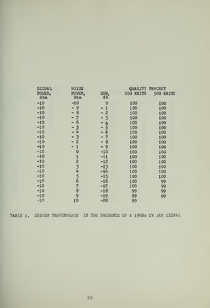
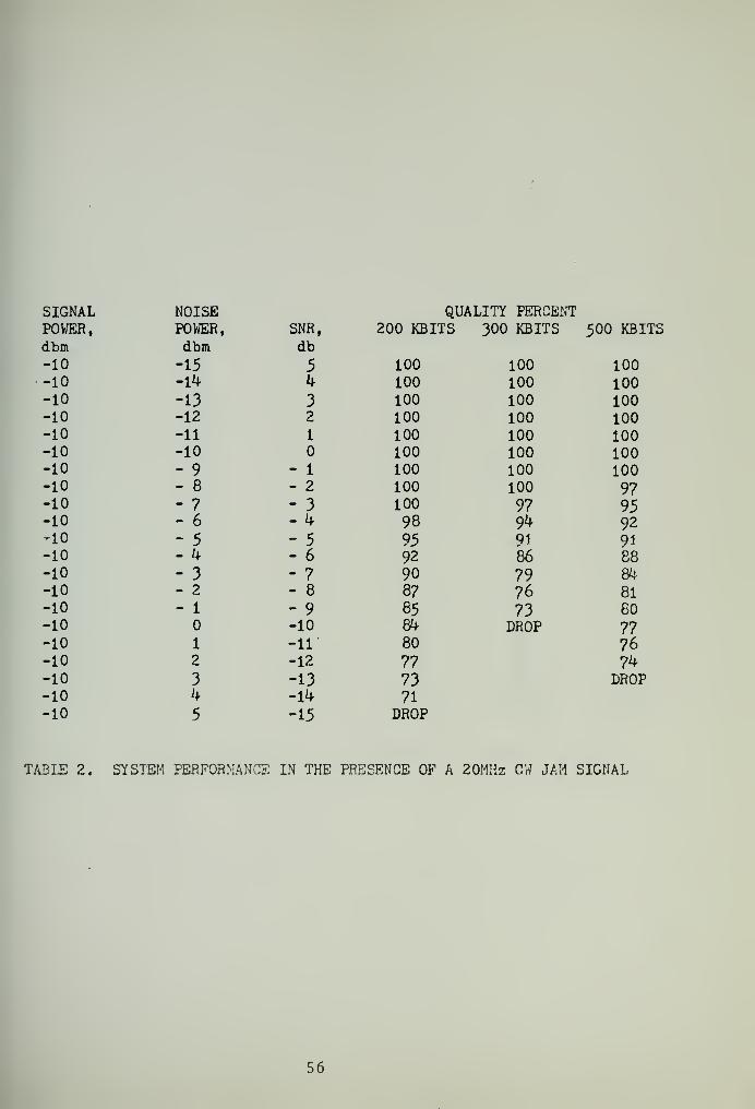
SIGNAL NOISE QUALITY PERCENTPOWER, POWER, SNR, 200 KBITS 500 KBITSdbm dbm db
-10 -10 100 100-10 - 9 - 1 100 100-10 - 8 - 2 100 100-10 - 7 - 3 100 100-10 - 6 - k 100 100-10 - 5 - 5 100 100-10 - 4 - 6 100 100-10 - 3 - 7 100 100-10 - 2 - 8 100 100-10 - 1 - 9 100 100-10 -10 100 100-10 1 -11 100 100-10 2 -12 100 100-10 3 -13 100 100-10 k -14 100 100-10 5 -15 100 100-10 6 -16 100 99-10 7 -17 100 99-10 8 -18 99 99-10 9 -19 99 99-10 10 -20 99
TABLE 1. SYSTEM PERFORMANCE IN THE PRESENCE OF A 19MHz CW JAM SIGNAL
55

SIGNAL NOISE QUALITY PERCENTPOWER, POWER, SNR, 200 KBITS 500 KBIdbm dbm db-10 -15 5 100 100 100-10 -14 4 100 100 100-10 -13 3 100 100 100-10 -12 2 100 100 100-10 -11 1 100 100 100-10 -10 100 100 100-10 - 9 - 1 100 100 100-10 - 8 - 2 100 100 97-10 - 7 - 3 100 97 95-10 - 6 - 4 98 94 92-10 - 5 - 5 95 91 91-10 - 4 - 6 92 86 88-10 - 3 - 7 90 79 84-10 - 2 - 8 87 76 81-10 - 1 - 9 85 73 80-10 -10 84 DROP 77-10 1 -11 80 76-10 2 -12 77 74-10 3 -13 73 DROP-10 4 -14 71-10 5 -15 DROP
TABLE 2. SYSTEM PERFORMANCE IN THE PRESENCE OF A 20MHz CW JAM SIGNAL
56

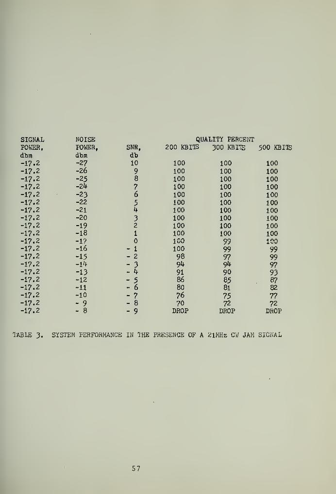
SIGNAL NOISE QUi\LITY PERCEiY.r
POWER, POWER, SNR, 200 KBITS 300 KBITS 500 kb:
dbm dbm db-17.2 -27 10 100 100 100-17.2 -26 9 100 100 100-17.2 -25 8 100 100 100-17.2 -24 7 100 100 100-17.2 -23 6 100 100 100-17.2 -22 5 100 100 100-17.2 -21 4 100 100 100-17.2 -20 3 100 100 100-17.2 -19 2 100 100 100-17.2 -18 1 100 100 100-17.2 -17 100 99 100-17.2 -16 - 1 100 99 99-17.2 -15 - 2 98 97 99-17.2 -i4 - ? 94 94 97-17.2 -13 - 4 91 90 93-17.2 -12 - 5 86 85 87-17.2 -11 - 6 80 81 82-17.2 -10 - 7 76 75 77-17.2 - 9 - 8 70 72 72-17.2 - 8 - 9 DROP DROP DROP
TABLE 3. SYSTEM PERFORMANCE IN THE PRESENCE OF A 21MHz CW JAM SIGNAL
57

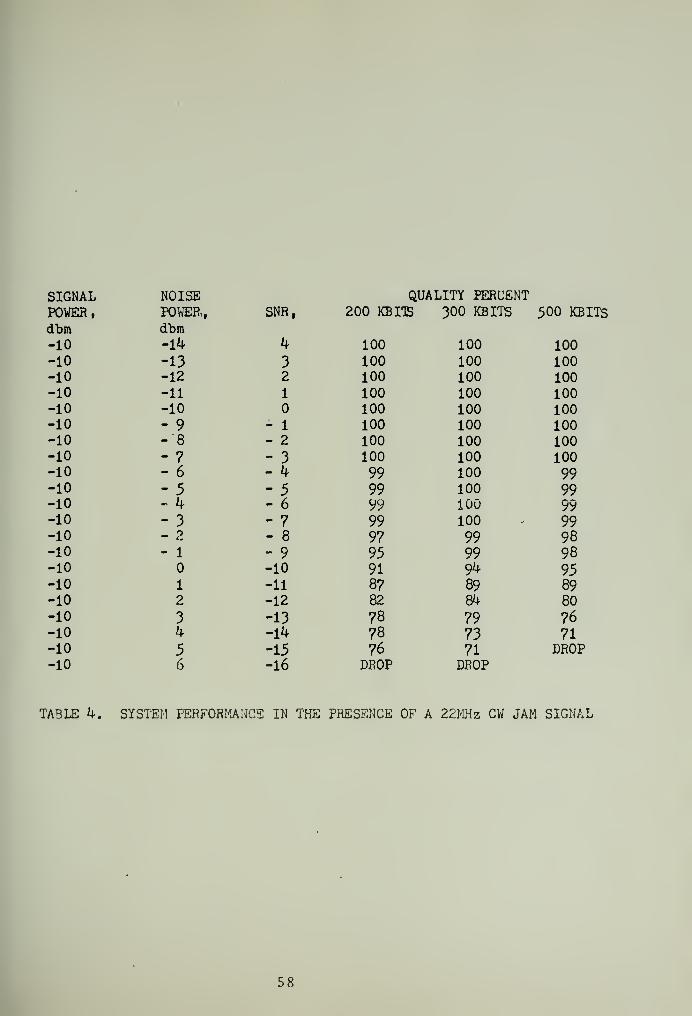
SIGNAL NOISE qua:LITY PERCENT
POWER, POWER, SNR, 200 KBITS 300 KBITS 500 KB
dbm dbm-10 -14 k 100 100 100-10 -13 3 100 100 100-10 -12 2 100 100 100-10 -11 1 100 100 100-10 -10 100 100 100-10 - 9 - 1 100 100 100-10 - 8 - 2 100 100 100-10 - 7 - 3 100 100 100-10 - 6 - 4 99 100 99-10 - 5 - 5 99 100 99-10 - tt - 6 99 100 99-10 - 3 - 7 99 100 99-10 - 8 97 99 98-10 - 1 - 9 95 99 98-10 -10 91 94 95-10 1 -11 87 89 89-10 2 -12 82 m 80-10 3 -13 78 79 76-10 4 -Ik 78 73 71-10 5 -15 76 71 DROP-10 6 -16 DROP DROP
TABLE k. SYSTEM PERFORMANCE IN THE PRESENCE OF A 22MHz CW jam signa:
58

SIGNAL NOISE QUALITY PERCENTPOWER. POWER, SNR, 200 KBITS 300 KBITS 500 KBdbm dbm db-10 -10 100 100 100-10 - 9 - 1 100 100 100-10 - 8 - 2 100 100 100-10 - 7 - 3 100 100 100-10 - 6 - k 100 100 100-10 - 5 - 5 100 100 100-10 - 4 - 6 100 100 100-10 - 3 - 7 100 100 100-10 - 2 - 8 100 100 100-10 - 1 - 9 100 100 100-10 -10 100 100 100-10 1 -11 100 100 100-10 2 -12 100 100 100-10 3 -13 100 100 96-10 k -14 100 98 89-10 5 -15 100 97 78-10 6 -16 99 91 73-10 7 -17 96 m DROP-10 8 -18 88 79-10 9 -19 81 73-10 10 -20 75 DROP-10 11 -21 DROP
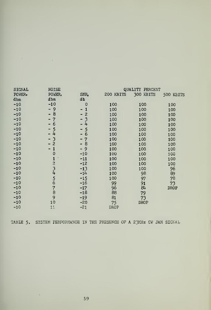
TABLE 5. SYSTEM PERFORMANCE IN THE PRESENCE OF A 23MHz CW JAM signa:
59
SIGNAL NOISE QU7ILITY PERCENTPOWER, POWER, SNR, 200 KBITS 300 KBITS 500 KBdbm dbm db-10 -10 100 100 100-10 - 9 - 1 100 100 100-10 - 8 - 2 100 100 100-10 - 7 - 3 100 ICO 100-10 - 6 - 4 100 100 100-10 - 5 - 5 100 100 100-10 - 4 - 6 100 100 100-10 - 3 - 7 100 100 100-10 - 2 - 8 100 100 100-10 - 1 - 9 100 100 100-10 -10 100 100 100-10 1 -11 100 99 100-10 2 -12 100 99 100-10 3 -13 100 99 95-10 4 -14 100 91 91-10 5 -15 98 87 -84
-10 6 -16 95 82 77-10 7 -17 90 78 72-10 8 -18 82 73 DROP-10 9 -19 75 DROP-10 10 -20 DROP
TABLE 6. SYSTEM PERFORMANCE IN THE PRESENCE OF A 24MHz CW JAM SIGNAL
60

SIGNAL NOISE QUJUITY PERCENTPOWER, POWER, SNR, 200 KBITS 300 KBITS 500 Hdbm dbm db-10 -10 100 100 100-10 - 9 - 1 100 100 100-10 - 8 - 2 100 100 100-10 - 7 - 3 100 100 100-10 - 6 - k 100 100 100-10 - 5 - 5 100 100 100-10 - k - 6 100 100 100-10 - 3 - 7 100 100 100-10 - 2 —8 100 100 100-10 - 1 - 9 100 100 100-10 -10 100 100-10 1 -11 100 100 100-10 2 -12 100 100 100-10 3 -13 100 100 100-10 4 -Ik 100 100 100-10 5 -15 100 100 100-10 6 -16 100 100 100-10 7 -17 100 100 100-10 8 -18 100 100 100-10 9 -19 100 100 100-10 10 -20 100 100 99-10 11 -21 100 98 98
TABLE 7. SYSTEM PERFORMANCE IN THE PRESENCE OF A 25MHz CW JAM SIGNAL
61

SIGNAL NOISE Qll\LITY PERCENTPOWER, POWER, SNR, 200 KBITS 300 KBITS 500 Hdbm dbm db-10 -15 5 1 100 100 100-10 -14 4 100 100 100-10 -13 3 100 100 100-10 -12 2 100 100 100-10 -11 1 100 100 100-10 -10 100 100 100-10 - 9 - 1 99 99 100-10 - 8 - 2 96 99 100-10 - 7 - 3 9^ 96 96-10 - 6 - 4 90 91 91-10 - 5 - 5 90 88 86-10 - 4 - 6 88 86 85-10 - 3 - 7 84 83 85-10 - 2 - 8 83 81 85-10 - 1 - 9 81 80 83-10 -10 80 80 81-10 1 -11 79 79 80-10 2 -12 76 79 80
TABLE 8. SYSTEM PERFORMANCE IN THE PRESENCE OF A WIDEBAND JAM SIGN)
62

frequency of the CW jammer coincides with the center fre-
quencies of the spread spectrum channel waveforms. Jamming
signals displaced from the center frequency of a spread
spectrum channel waveform by 1 MHz required approximately
6 to 7 more db of power to have as much effect on the sys-
tem's performance as a jamming signal in the center of a
channel waveform. Each additional displacement by 1 MHz
showed a reduction of about 5 db in the effectiveness of
the jamming signal.
With a CW jam signal placed in the center of a channel
waveform, the system copies solidly at a signal-to-noise
ratio of -1 db and dropped synchronization at a signal-to-
noise ratio of -9 db
.
These tests also showed that the system can be used to
transmit data at a data rate of 500 KBITS without more than
a 2 db degradation in processing gain.
The wideband noise test revealed that the system is
capable of copying solidly in a wideband noise environment
which yields a signal-to-noise ratio of -1 db , and it will
copy without losing synchronization at signal-to-noise
ratios of -12 db or greater.
The synchronization referred to in the previous para-
graphs has nothing to do with the transmitter- to-receive
synchronization. No such synchronization is necessary in
a simple ASWD system. The method used to record received
message quality involved a frequency counter which would
lose synchronization with the pulse train when noise power
became sufficiently large to produce triggering spikes.
63

This was not considered to be an unrealistic constraint on
the system, as any data train requires some method of syn-
chronization before the data can be processed.
64

VII. CONCLUSION
This thesis effort resulted in a laboratory system
capable of satisfying many of the objectives sought at the
outset of the investigation. Based on the results of tests
performed on the system, a processing gain of approximately
19 db was realized. Since the bandwidth spreading ratio of
20 to 1 predicts 13 db of processing gain. It is felt that
6 db of processing gain are attributable to the Golay cod-
ing scheme of the ASWD pair. Whereas the system has not yet
been consolidated into a compact form, the transmitter when
transformed from a laboratory system to a portable "toy"
should weight between 16 and 2 4 ounces, and the receiver
should weigh just over three pounds.
The specification of simplicity was completely satisfied
as witnessed by the design and fabrication sections of this
thesis. The fact that only a laboratory system was tested
and reported on instead of a completed portable system is
a factor imposed by time and the unpredictable shortages of
critical devices and components.
Several areas of follow-on work are suggested by the
efforts and results of this thesis work. Perhaps the most
obvious one is improvements on the spread spectrum system
capable of RPV usage at S-band frequencies. A longer se-
quence of ASWD codes could be used to give the system an
improvement in both communications security as well as
transmission security. A PN code modulator could be added
65

to the system to give each further communications security
and processing gain.
Another area of follow-on work suggested by this thesis
is a thorough investigation to determine the exact effect
of Golay complementary coding on the processing gain of a
spread spectrum system. Much of this investigation could
be performed using simple MODEM'S without the necessity of
signal transmissions.
Covert transmission of video data is within the reach
of current technology. This is the driving force that makes
spread spectrum research challenging and rewarding.
66

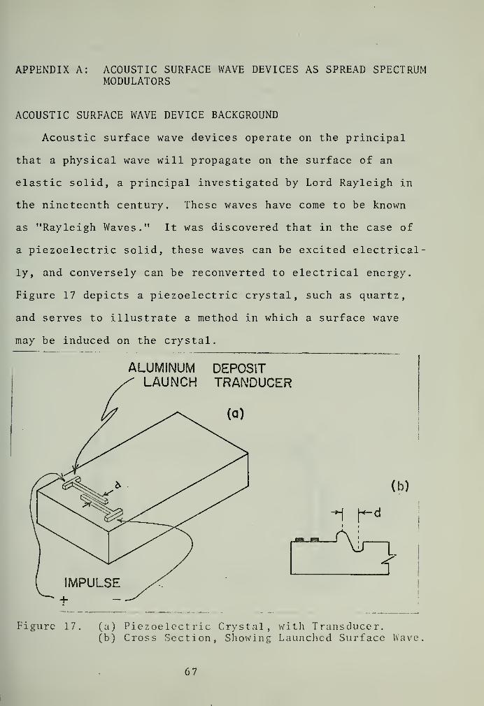
APPENDIX A: ACOUSTIC SURFACE WAVE DEVICES AS SPREAD SPECTRUMMODULATORS
ACOUSTIC SURFACE WAVE DEVICE BACKGROUND
Acoustic surface wave devices operate on the principal
that a physical wave will propagate on the surface of an
elastic solid, a principal investigated by Lord Rayleigh in
the nineteenth century. These waves have come to be known
as "Rayleigh Waves." It was discovered that in the case of
a piezoelectric solid, these waves can be excited electrical
ly, and conversely can be reconverted to electrical energy.
Figure 17 depicts a piezoelectric crystal, such as quartz,
and serves to illustrate a method in which a surface wave
may be induced on the crystal.
ALUMINUM DEPOSITLAUNCH TRANDUCER
(b)
.ra.
1 f-d
Air-}
Figure 17. (a) Piezoelectric Crystal, with Transducer.(b) Cross Section, Showing Launched Surface Wave
67

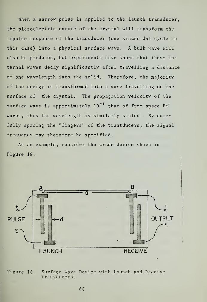
When a narrow pulse is applied to the launch transducer,
the piezoelectric nature of the crystal will transform the
impulse response of the transducer (one sinusoidal cycle in
this case) into a physical surface wave. A bulk wave will
also be produced, but experiments have shown that these in-
ternal waves decay significantly after travelling a distance
of one wavelength into the solid. Therefore, the majority
of the energy is transformed into a wave travelling on the
surface of the crystal. The propagation velocity of the
surface wave is approximately 10 that of free space EM
waves, thus the wavelength is similarly scaled. By care-
fully spacing the "fingers" of the transducers, the signal
frequency may therefore be specified.
As an example, consider the crude device shown in
Figure 18.
PULSE OUTPUT
LAUNCH RECEIVE
Figure 18. Surface Wave Device with Launch and ReceiveTransducers
.
68

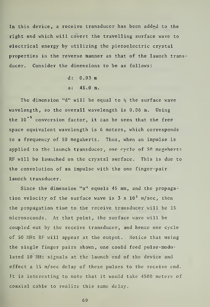
In this device, a receive transducer has been add*;d to the
right end which will covert the travelling surface wave to
electrical energy by utilizing the piezoelectric crystal
properties in the reverse manner as that of the launch trans
ducer. Consider the dimensions to be as follows:
d: 0.03 m
a: 45.0 m.
The dimension "d" will be equal to h the surface wave
wavelength, so the overall wavelength is 0.06 m. Using
the 10 conversion factor, it can be seen that the free
space equivalent wavelength is 6 meters, which corresponds
to a frequency of 50 megahertz. Thus, when an impulse is
applied to the launch transducer, one cycle of 50 megahertz
RF will be launched on the crystal surface. This is due to
the convolution of an impulse with the one finger-pair
launch transducer.
Since the dimension "a" equals 45 mm, and the propaga-
tion velocity of the surface wave is 3 x 10 3 m/sec, then
the propagation time to the receive transducer will be 15
microseconds. At that point, the surface wave will be
coupled out by the receive transducer, and hence one cycle
of 50 MHz RF will appear at the output. Notice that using
the single finger pairs shown, one could feed pulse-modu-
lated 50 MHz signals at the launch end of the device and
effect a 15 m/sec delay of these pulses to the receive end.
It is interesting to note that it would take 4500 meters of
coaxial cable to realize this same delay.
69

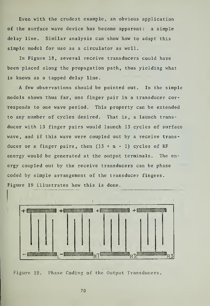
Even with the crudest example, an obvious application
of the surface wave device has become apparent: a simple
delay line. Similar analysis can show how to adapt this
simple model for use as a circulator as well.
In Figure 18, several receive transducers could have
been placed along the propagation path, thus yielding what
is known as a tapped delay line.
A few observations should be pointed out. In the simple
models shown thus far, one finger pair in a transducer cor-
responds to one wave period. This property can be extended
to any number of cycles desired. That is, a launch trans-
ducer with 13 finger pairs would launch 13 cycles of surface
wave, and if this wave were coupled out by a receive trans-
ducer or n finger pairs, then (13 + n - 1) cycles of RF
energy would be generated at the output terminals. The en-
ergy coupled out by the receive transducers can be phase
coded by simple arrangement of the transducer fingers.
Figure 19 illustrates how this is done.
Figure 19. Phase Coding of the Output Transducers.
70

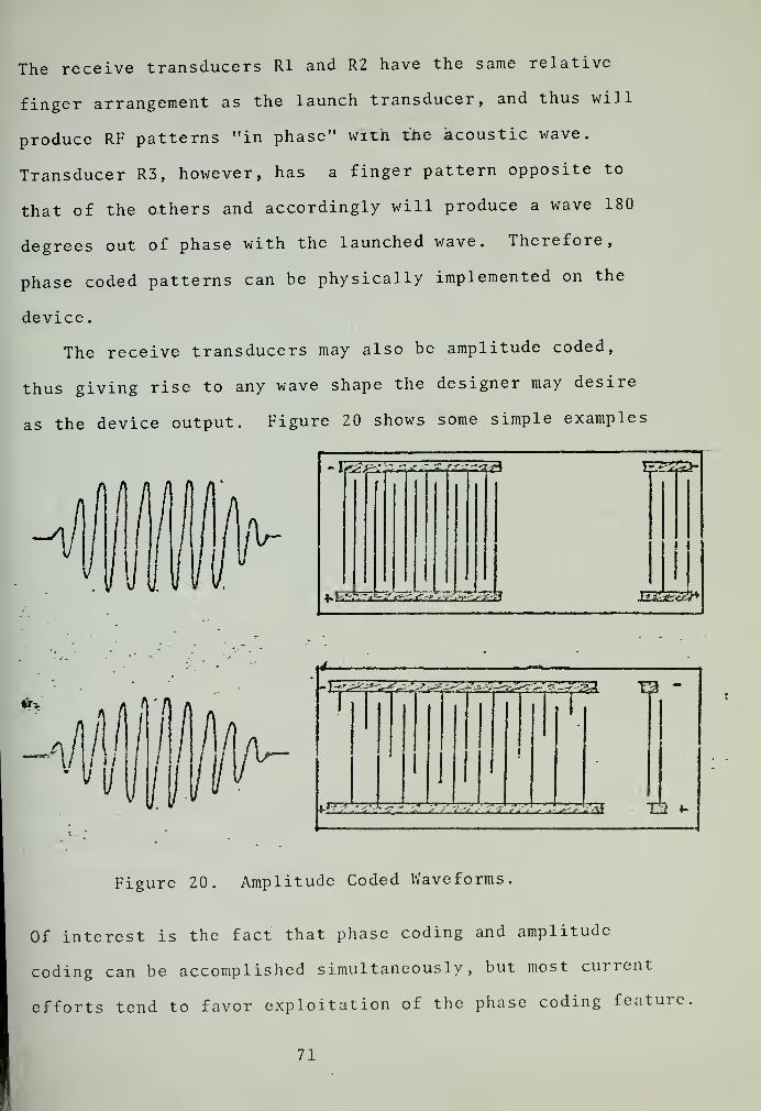
The receive transducers Rl and R2 have the same relative
finger arrangement as the launch transducer, and thus will
produce RF patterns "in phase" witn the acoustic wave.
Transducer R3, however, has a finger pattern opposite to
that of the others and accordingly will produce a wave 180
degrees out of phase with the launched wave. Therefore,
phase coded patterns can be physically implemented on the
device.
The receive transducers may also be amplitude coded,
thus giving rise to any wave shape the designer may desire
as the device output. Figure 20 shows some simple examples
-l*s££b& gSEja
\-Wrr.:t %-£-e-r.i',^risSSasal E2SEg*
*>-I SIZSS^
r^ j> ' * ^ \ st
:s
'* '' ' 1-"' - * '* ' ' *' - .--*-"^£3
13 -
13 *-
Figure 20. Amplitude Coded Waveforms.
Of interest is the fact that phase coding and amplitude
coding can be accomplished simultaneously, but most current-
efforts tend to favor exploitation of the phase coding feature
71

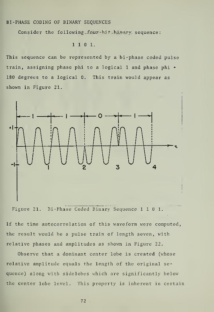
BI -PHASE CODING OF BINARY SEQUENCES
Consider the following ...four-b.i *..b£n?ry. sequence :
110 1.
This sequence can be represented by a bi-phase coded pulse
train, assigning phase phi to a logical 1 and phase phi +
180 degrees to a logical 0. This train would appear as
shown in Figure 21.
1\J U
Figure 21. Bi-Phase Coded Binary Sequence 110 1.
If the time autocorrelation of this waveform were computed,
the result would be a pulse train of length seven, with
relative phases and amplitudes as shown in Figure 22.
Observe that a dominant center lobe is created (whose
relative amplitude equals the length of the original se-
quence) along with sidelobes which are significantly below
the center lobe level. This property is inherent in certain
72

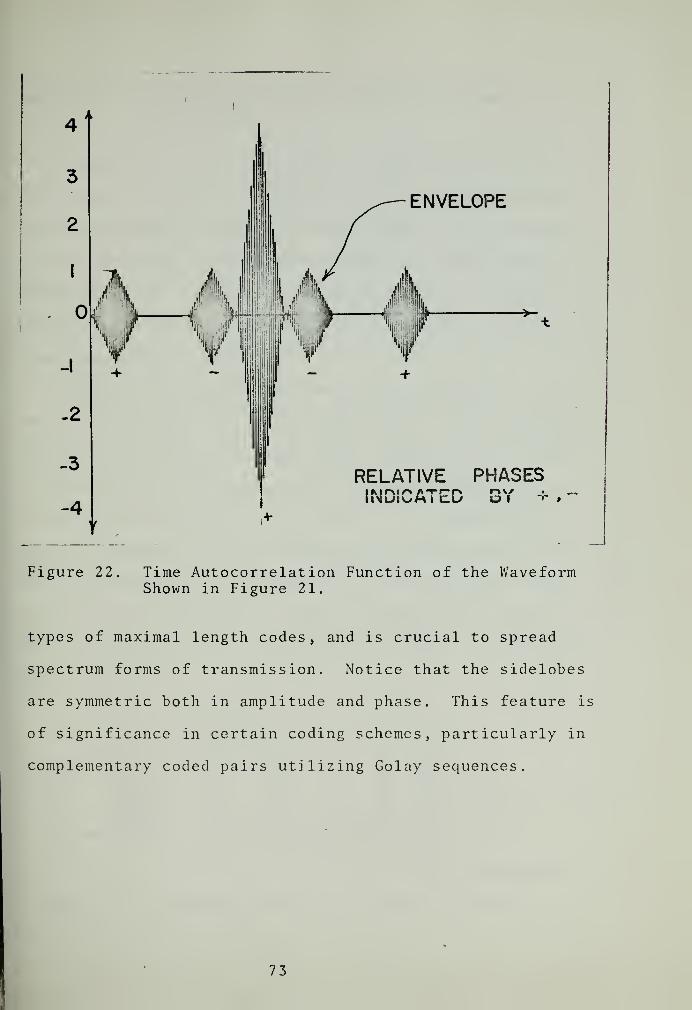
ENVELOPE
RELATIVE PHASESINDICATED BY +
Figure 22. Time Autocorrelation Function of the WaveformShown in Figure 21.
types of maximal length codes, and is crucial to spread
spectrum forms of transmission. Notice that the sidelobes
are symmetric both in amplitude and phase. This feature is
of significance in certain coding schemes, particularly in
complementary coded pairs utilizing Golay sequences.
73

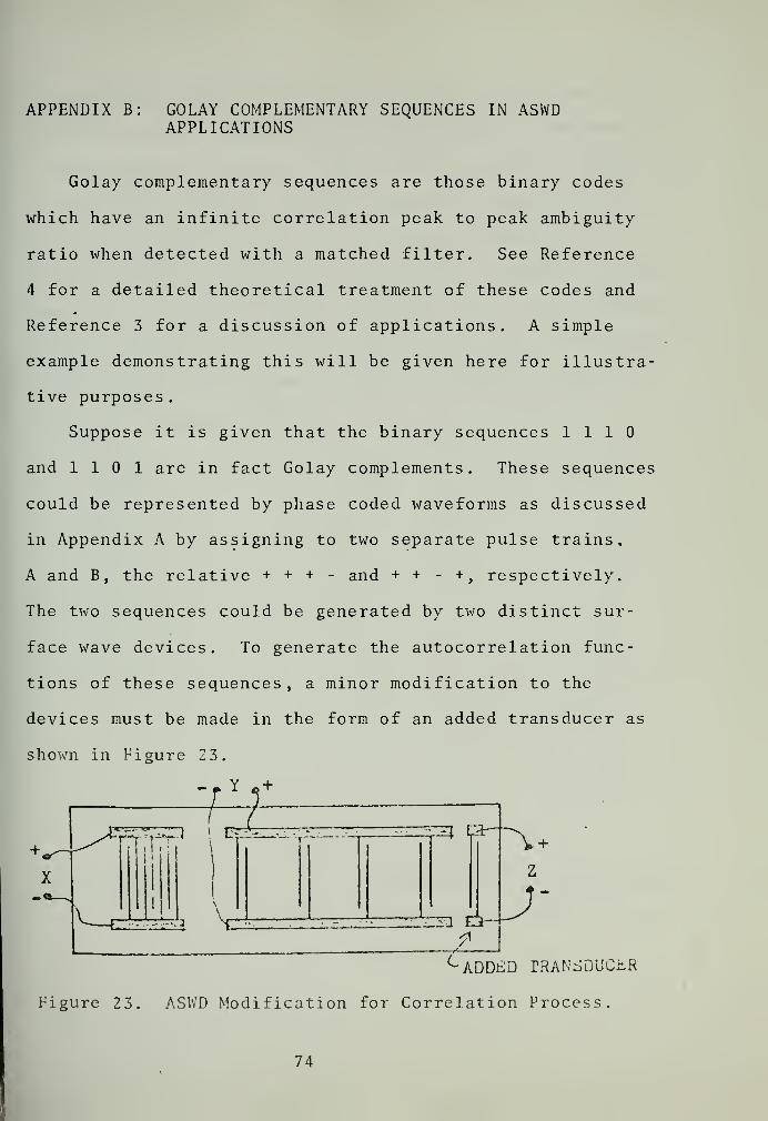
APPENDIX B: GOLAY COMPLEMENTARY SEQUENCES IN ASWDAPPLICATIONS
Golay complementary sequences are those binary codes
which have an infinite correlation peak to peak ambiguity
ratio when detected with a matched filter. See Reference
4 for a detailed theoretical treatment of these codes and
Reference 3 for a discussion of applications. A simple
example demonstrating this will be given here for illustra-
tive purposes
.
Suppose it is given that the binary sequences 1110and 110 1 are in fact Golay complements. These sequences
could be represented by phase coded waveforms as discussed
in Appendix A by assigning to two separate pulse trains,
A and B, the relative + + + - and + + - +, respectively.
The two sequences could be generated by two distinct sur-
face wave devices. To generate the autocorrelation func-
tions of these sequences, a minor modification to the
devices must be made in the form of an added transducer as
shown in Figure 23.
C ADDt:D TRANSDUCER
Figure 23. ASWD Modification for Correlation Process.
74

Assuming one device for each of the codes, the process would
be as follows: If both ASWD's were excited by the same im-
pulse, applied at port X, then the two waveforms coupled out
from port Y would be of equal length and would be phase co-
herent. A matched filter technique would then be used to
generate the autocorrelation functions. Consider the case
of code A. If the bi-phase representation of this code was
fed to port Y of its matched ASWD, then the autocorrelation
function R.. would appear at port Z. Tabular computation
of R.« is given in Table 9.
TIME A*A RAA
1 + + + -
+++- - 1
2 +++- - 1+ + +-
3 +++- - 1 1
+ + + -
4 +++- - 1 1 4
+ + + -
5 +++- - 1 1 4 1
+ + + -
6 +++- - 1 1 4 1
+ + + -
7 +++- -10 14 10-1+ + + -
Table 9. Computation of R...
The sequence -10 14 10-1 represents the relative phases
and amplitudes of the pulses comprising the function Rj,,
Similar analysis for code B would yield R„B
equal to
10-14-10 1. The property of the Golay codes is such
that the algebraic sum of the autocorrelation functions
75

must be obtained to produce the resultant correlation
function. This function is shown in Figure 24. The re-
sultant correlation sequence is then 8 0, which
exhibits the property of an infinite major peak to sidelobe
R^: -10 14 10-1
RBB
: 10-14-10 1
RAA+ R
BB: 8
Figure 24. Summing R., and RRR to Obtain the Correlation.
peak ratio, in addition to a 3 db major peak gain over the
single code case. Since this is the best theoretically ob-
tainable correlation result (least probability of ambiguity
between the major peak and sidelobe peaks,) then it was
hypothesized that in practice it would also be the best
result.
The increased processing gain (conventional codes
would yield a final correlation peak of amplitude 4 with
the addition of existing sidelobes) imply that in a noisy
environment this coding scheme would be superior.
76

APPENDIX C: CHARACTERISTICS OF SYSTliM ACOUSTIC SURFACE WAVEDEVICES
Appendix A of Reference 2 contains a detailed descrip-
tion of the electrical characteristics and of the coding
scheme ASWD's used in the transceiver system of this thesis.
Relevant portions of the description are repeated here for
report continuity purposes.
Figure 25 shows a photograph of one of the ASWD's as
it was connected in the circuit. The casing in which the
device is mounted was milled out of a solid block of aluminum
Figure 25. ASWD with External Connections
that measures 4 inches long by 2.2 inches wide by one inch
thick. The top of the casing, seen in the photograph, was
milled to allow sufficient space to mount the quartz substrate
77
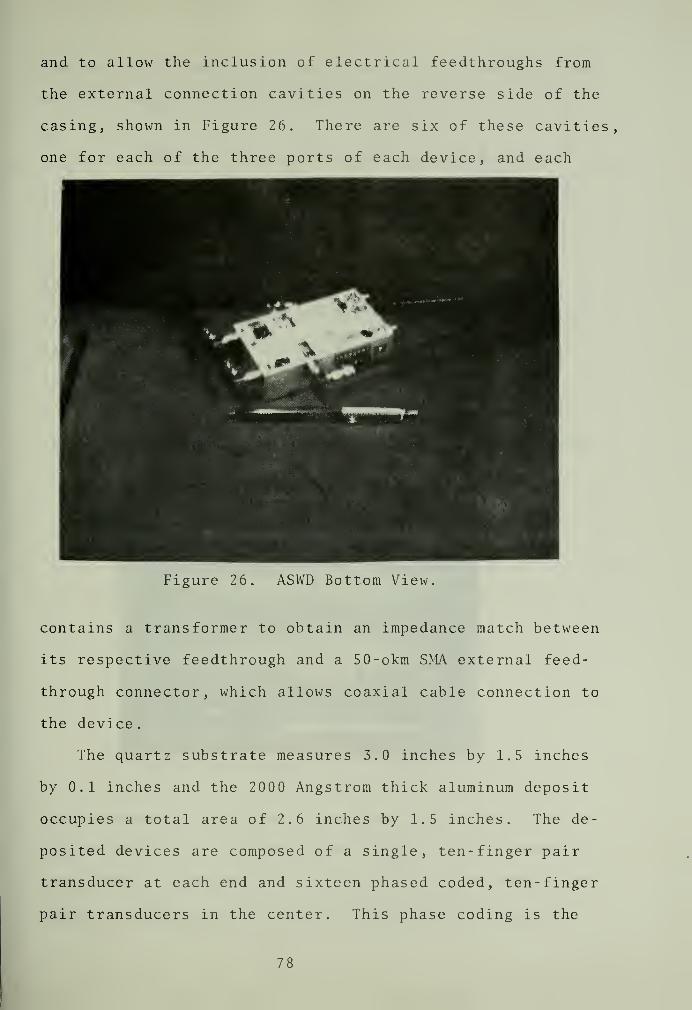
and to allow the inclusion of electrical feedthroughs from
the external connection cavities on the reverse side of the
casing, shown in Figure 26. There are six of these cavities,
one for each of the three ports of each device, and each
Figure 26. ASWD Bottom View.
contains a transformer to obtain an impedance match between
its respective feedthrough and a 50-okm SMA external feed-
through connector, which allows coaxial cable connection to
the device.
The quartz substrate measures 3.0 inches by 1.5 inches
by 0.1 inches and the 2000 Angstrom thick aluminum deposit
occupies a total area of 2.6 inches by 1.5 inches. The de-
posited devices are composed of a single, ten-finger pair
transducer at each end and sixteen phased coded, ten-finger
pair transducers in the center. This phase coding is the
7!
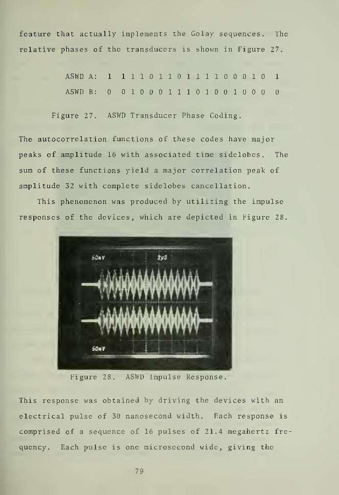
feature that actually implements the Golay sequences. The
relative phases of the transducers is shown in Figure 27.
ASWD A: 1 1110110111100010 1
ASWD B: 0100011101001000
Figure 27. ASWD Transducer Phase Coding.
The autocorrelation functions of these codes have major
peaks of amplitude 16 with associated time sidelobes. The
sum of these functions yield a major correlation peak of
amplitude 32 with complete sidelobes cancellation.
This phenomenon was produced by utilizing the impulse
responses of the devices, which are depicted in Figure 28.
Figure 28. ASWD Impulse Response.
This response was obtained by driving the devices with an
electrical pulse of 30 nanosecond width. Each response is
comprised of a sequence of 16 pulses of 21.4 megahertz fre-
quency. Each pulse is one microsecond wide, giving the
79

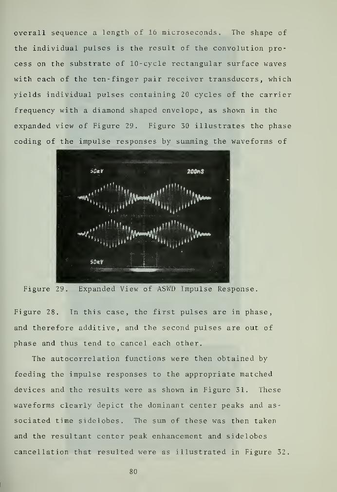
overall sequence a length of 16 microseconds. The shape of
the individual pulses is the result of the convolution pro-
cess on the substrate of 10-cycle rectangular surface waves
with each of the ten-finger pair receiver transducers, which
yields individual pulses containing 20 cycles of the carrier
frequency with a diamond shaped envelope, as shown in the
expanded view of Figure 29. Figure 30 illustrates the phase
coding of the impulse responses by summing the waveforms of
200nS
>"<M''V*
,
"""»»!
i *mv>-4
%w
Figure 29. Expanded View of ASWD Impulse Response
Figure 28. In this case, the first pulses are in phase,
and therefore additive, and the second pulses are out of
phase and thus tend to cancel each other.
The autocorrelation functions were then obtained by
feeding the impulse responses to the appropriate matched
devices and the results were as shown in Figure 31. These
waveforms clearly depict the dominant center peaks and as-
sociated time sidelobes. The sum of these was then taken
and the resultant center peak enhancement and sidelobes
cancellation that resulted were as illustrated in Figure 32.
80
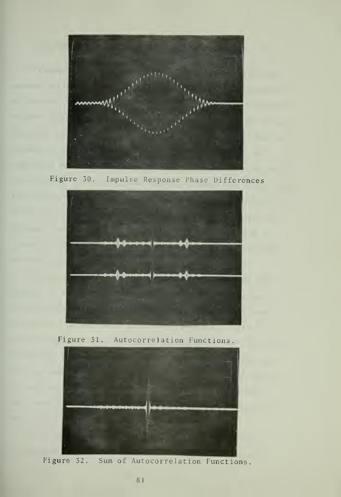
,-•"',
/^vw^,l|.
Figure 30. Impulse Response Phase Differences
Figure 31. Autocorrelation Functions
Figure 32. Sum of Autocorrelation Functions
APPENDIX D: SYNCHRONIZATION CONSIDERATIONS
Frequency Hop and Pseudo Noise code spread spectrum
communications systems utilize PN codes in the transmitter
to encode the information signal: to spread the bandwidth
of the information signal; or more generally, to do a com-
bination of the two. For faithful reproduction of the in-
formation signal in the receiver(s) of the system, an
identical PN code must be provided to the receiver(s) which
is in exact synchronization with the transmitter code. Ini-
tial synchronization is accomplished by slewing one of the
codes with respect to the other until a usable output in-
dicates synchronization. (Usually the receiver code is
slewed through the code pattern; but in some systems the
transmitter PN pattern is slewed for searching.)
If the components of the system were stationary with
respect to each other, the signal paths were invariant,
and the code rates in all of the subsystems of the com-
munications network were precisely identical, initial
synchronization would be sufficient to guarantee continuous
subsequent synchronization. But since none of these con-
ditions usually prevail, it is necessary that some method
of code tracking be provided to compensate for factors
which would otherwise tend to break the synchronization of
the codes
.
Since spread spectrum modulation via ASWD's does not
involve the use of a PN code pattern, the sophisticated
82

circuitry of PN code synchronization is avoided in this
latter method. A sacrifice oi tiit vk''pattern precludes a
system from obtaining some of the advantages usually as-
sociated with spread spectrum techniques such as ranging
(by measuring code delay time) , multiple access (through
appropriate code selection) , and high degree of communica-
tions security (by providing an easy method of code sub-
stitutions) . In applications where the sacrifice of these
features does not effect the requirements of the system, a
significant savings in simplicity and space can be gained
by employing ASWD's for generation of the spread spectrum
waveform.
83

LIST OF MJFHkHnlxs
1. Means, R. W. , Speiser, J. M., and Whitehouse, H. J.,Image Transmission Via Spread Spectrum Techniques
,
ARPA Quarterly Technical Report, (June 1, 1973 -
October 31, 1973), Naval Underseas Center, SanDiego, 1973.
2. Cocci, J. A., A Spread Spectrum Communication Technique,
Engineer' s Thesis, Naval Postgraduate School,Monterey, California, September 1973.
3. French, C. E., Totally Orthogonal Complementary BinaryCoded Sequences and Applications to CommunicationsSystems , MS Thesis, Naval Postgraduate School,Monterey, California, June 1971.
4. Jauregui , S., Jr., A Theoretical Study of ComplementaryBinary Code Sequences and a Computer Search forNew Kernels , Ph. D. Thesis , Naval Postgraduate School
,
Monterey, California, May 1962.
5. Advisory Group on Atmospheric Research and Development,Spread Spectrum Communications , 1973.
6. Hughes Aircraft Company, Wideband Command and ControlModem, Final Technical Report, December 1972.
84

INITIAL DISTRIBUTION LIST
No. Copies
1. Defense Documentation Center 2
Cameron StationAlexandria, Virginia 22314
2. Library, Code 0212 2
Naval Postgraduate SchoolMonterey, California 93940
3. Assoc Professor S. Jauregui, Jr., Code 52Ja 10Department of Electrical EngineeringNaval Postgraduate SchoolMonterey, California 93940
4. Professor P. E. Cooper, Code 52Cp 1
Department of Electrical EngineeringNaval Postgraduate SchoolMonterey, California 93940
5. LCDR Cain Garrett, Jr. 1
COMCRUDESGRU FIVEFPO San Francisco 96601
6. LT Laird W. Stanton 1
Operations DepartmentUSS Hancock CVA 19FPO San Francisco 96601
7. Commander . 1
Naval Undersea CenterSan Diego, California 92132
Attn: Code 6003Mr. Harper Whitehouse
8. Commander 1
Naval Air Svstems CommandWashington,' D. C. 20360
Attn: Code 5371Mr. S. Vogt
9. Hughes Aircraft Company 1
Ground Systems DivisionFullerton, California
Attn: Mr. James A. KivettBldg. 600/E228

10. CommanderNaval Security Group Command3801 Nebraska Avenue, N.W.Washington, D. C. 20390
Attn: G80CDR H. Orejuela
11. Naval Electronics Systems CommandNaval Electronics Systems Command HeadquartersWashington, D. C. 20360
Attn: PME 10 7
LCDR R. Shields
12. DirectorNational Security AgencyFort Meade, Maryland 20755
Attn: W. Group J. Boone
13. DirectorNational Security AgencyFort Meade, Maryland
Attn: R. Group
14. Dean of ResearchNaval Postgraduate SchoolMonterey, California 93940
Attn: Code 023
Mr. C. B. Kelley
15. Naval ElectronicsNaval ElectronicsWashington, D. C.
Attn:
Systems CommandSystems Command Headquarters20360PME 10 7
LCDR A. Sagerian
16. Naval Electronics Laboratory Center271 Catalina Blvd.San Diego, California 92152
Attn: LT W. Gadino
17. Naval ElectronicsNaval ElectronicsWashington, D. C.
Attn:
SystemsSystems20360Code 03CDR Floyd H
CommandCommand Headquarters
Hollister
86


/
156^311Ga rrett
C°^e
a t
d
/o
S
nPeCtr^
9 3 6 t,
Thesis
G196 Garrettc.l A spread spectrum
communication svstem.
1rG /^ 3 U
thesG196
A sperad spectrum communication system.
3 2768 001 00583 8DUDLEY KNOX LIBRARY