Embed Size (px)
Citation preview
3236 IEEE TRANSACTIONS ON ELECTRON DEVICES, VOL. 55, NO. 11, NOVEMBER 2008
A Study of On-Chip StackedMultiloop Spiral Inductors
Kai Yang, Wen-Yan Yin, Senior Member, IEEE, Jinglin Shi, Kai Kang,Jun-Fa Mao, Senior Member, IEEE, and Y. P. Zhang
Abstract—This paper proposes a new differential topology thatfeatures a stacked multiloop inductor. Comparative studies ofstacked one- to four-loop spiral inductors with and without pat-terned ground shields (PGSs) for silicon-based radio-frequencyintegrated circuits (RFICs) were conducted, and lumped-elementcircuit models were developed for these inductors. The partial-element equivalent-circuit method that can accurately analyzemutual inductive couplings among different spirals in thesemultiloop geometries was employed for capturing the frequency-dependent inductances and resistances of inductors at low fre-quencies. A good agreement between numerical results andmeasurements is obtained. It is demonstrated that a stacked multi-loop spiral inductor with differential topology and PGS has alarger inductance and a higher Q-factor as compared with thesame inductor without differential topology and PGS. This hybridmethodology could provide a promising technique for developingnew silicon-based passive devices used in RFICs.
Index Terms—Differential topology, inductance, partial-element equivalent-circuit (PEEC) method, patterned groundshields (PGSs), Q-factor, resistance, stacked multiloop spiralinductors.
I. INTRODUCTION
IN THE PAST decade, CMOS silicon-based spiral inductorshave drawn considerable attentions due to their wide ap-
plications in radio-frequency integrated circuits (RFICs). Withrespect to different geometries and layouts of single-spiral in-ductors, some frequency-dependent and frequency-independentlumped-element circuit models (LECMs) have been developedand further implemented in the design of circuits [1], [2]. Fora silicon-based spiral inductor, the conductive loss of all metaltracks and the eddy-current loss in the silicon substrate [3] need
Manuscript received March 13, 2008; revised July 30, 2008. Current versionpublished October 30, 2008. This work was supported in part by the NationalNatural Science Fund of China (NSF) under Grant 90607011, by the NSF underGrant 60521002 for Creative Research Groups via SJTU, and by the Ministry ofEducation of China under Grant 20050248051 of the Doctoral Research Fund.The review of this paper was arranged by Editor M. J. Kumar.
K. Yang was with the Center for Microwave and RF Technologies, Schoolof Electronic Information and Electrical Engineering, Shanghai Jiao Tong Uni-versity, Shanghai 200240, China. He is now with the Department of ElectronicEngineering, The Chinese University of Hong Kong, Shatin, NT, Hong Kong(e-mail: [email protected]).
W.-Y. Yin and J.-F. Mao are with the Center for Microwave and RF Technolo-gies, School of Electronic Information and Electrical Engineering, ShanghaiJiao Tong University, Shanghai 200240, China (e-mail: [email protected]).
J. Shi and K. Kang are with the Integrated Circuits and Systems Laboratory,Institute of Microelectronics, Singapore 117685.
Y. P. Zhang is with the School of Electrical and Electronic Engineering,Nangyan Technological University, Singapore 639798.
Color versions of one or more of the figures in this paper are available onlineat http://ieeexplore.ieee.org.
Digital Object Identifier 10.1109/TED.2008.2004648
to be reduced so as to increase its Q-factor. Differential spiralinductors have been successfully introduced and employed [4]to provide higher Q-factors in differential circuits.
In addition, in order to increase Q-factors, a patterned groundshield (PGS), first proposed in [5], can be implemented be-tween the metal spiral and the silicon substrate [6]. Morerecently, Cheung and Long [7] studied shielding effects ofdifferent PGSs used for silicon-based monolithic microwaveand millimeter-wave integrated circuits. The presence of aPGS may cause additional parasitic capacitance, resulting inthe reduction of self-resonant frequency of the spiral inductor.Physically, it can be predicted that the combination of thedifferential topology and PGS technique may be a much betterchoice for enhancing the performance of most silicon-basedpassive devices. In circuit designs, on-chip spiral inductors withlarger inductance and smaller area are always highly desired,and therefore, two- or multispiral stacked geometries may beconsidered [8]–[10].
In this paper, differential topology is applied to explore high-performance on-chip stacked multiloop inductors which weredesigned and fabricated using a 0.18-μm RF CMOS process.It is demonstrated that the differential topologies with PGScan be an efficient solution for enhancing the performance ofmultiloop inductors with the same structure.
II. TOPOLOGIES OF ON-CHIP STACKED
MULTILOOP SPIRAL INDUCTORS
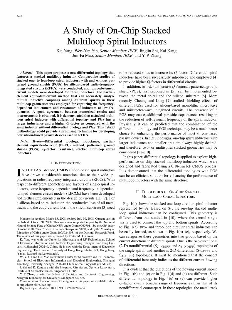
Fig. 1(a) shows the stacked one-loop circular spiral inductorrepresented by S1. Based on S1, the on-chip stacked multi-loop spiral inductors can be configured. This geometry isdifferent from that studied in [10], where the central singlevia is used to connect the top and bottom spirals. Accordingto Fig. 1(a), two- and three-loop circular spiral inductors canbe easily formed, as shown in Fig. 1(b)–(e), respectively. Wecan categorize these geometries into two groups based on thecurrent directions in different spirals. One is the two-directional(2-D) nondifferential (S2−NDIFF and S3−NDIFF) topologies ofthe single spiral, and another is 2-D differential (S2−DIFF andS3−DIFF) topologies. It must be mentioned that the conceptof differential here only indicates the different current flowingdirections.
It is evident that the directions of the flowing current shownin Fig. 1(b) and (c) or in Fig. 1(d) and (e) are different. Suchdifferential topology in Fig. 1(c) or (e) can provide higherQ-factor over a broader range of frequencies than that of itsnondifferential counterpart. In these topologies, the metal track
0018-9383/$25.00 © 2008 IEEE
YANG et al.: STUDY OF ON-CHIP STACKED MULTILOOP SPIRAL INDUCTORS 3237
Fig. 1. Two-directional nondifferential and differential topologies of one-to three-loop stacked spiral inductors. (a) S1. (b) S2−NDIFF. (c) S2−DIFF.(d) S3−NDIFF. (e) S3−DIFF.
Fig. 2. Three-directional nondifferential and differential topologies of thestacked four-loop spiral inductors. (a) S4−NDIFF. (b) S4−DIFF.
width is W , track spacing is S, and inner radius denoted by Ris exactly the same. On the other hand, following the similarway as shown in Fig. 1(c) and (e), the two- and three-loopdifferential topologies of stacked square and octagonal spiralinductors can also be constructed, but their geometries are notshown here.
Furthermore, Fig. 2(a) and (b) shows the three-directional(3-D) nondifferential (S4−NDIFF) and differential (S4−DIFF)topologies of stacked four-loop spiral inductors, respectively.The top and bottom spirals are also designed to have the sameinner radius (R) as in Fig. 1(a)–(e) earlier. The current directionshown in Fig. 2(b) is just in a reverse direction as in Fig. 2(a),and such unique differential implementation will be useful forthe enhancement in its Q-factor, which will be demonstratedexperimentally as follows. Table I lists the area information ofall the inductors studied.
TABLE ICOMPARISON OF THE AREA OF DIFFERENT INDUCTORS
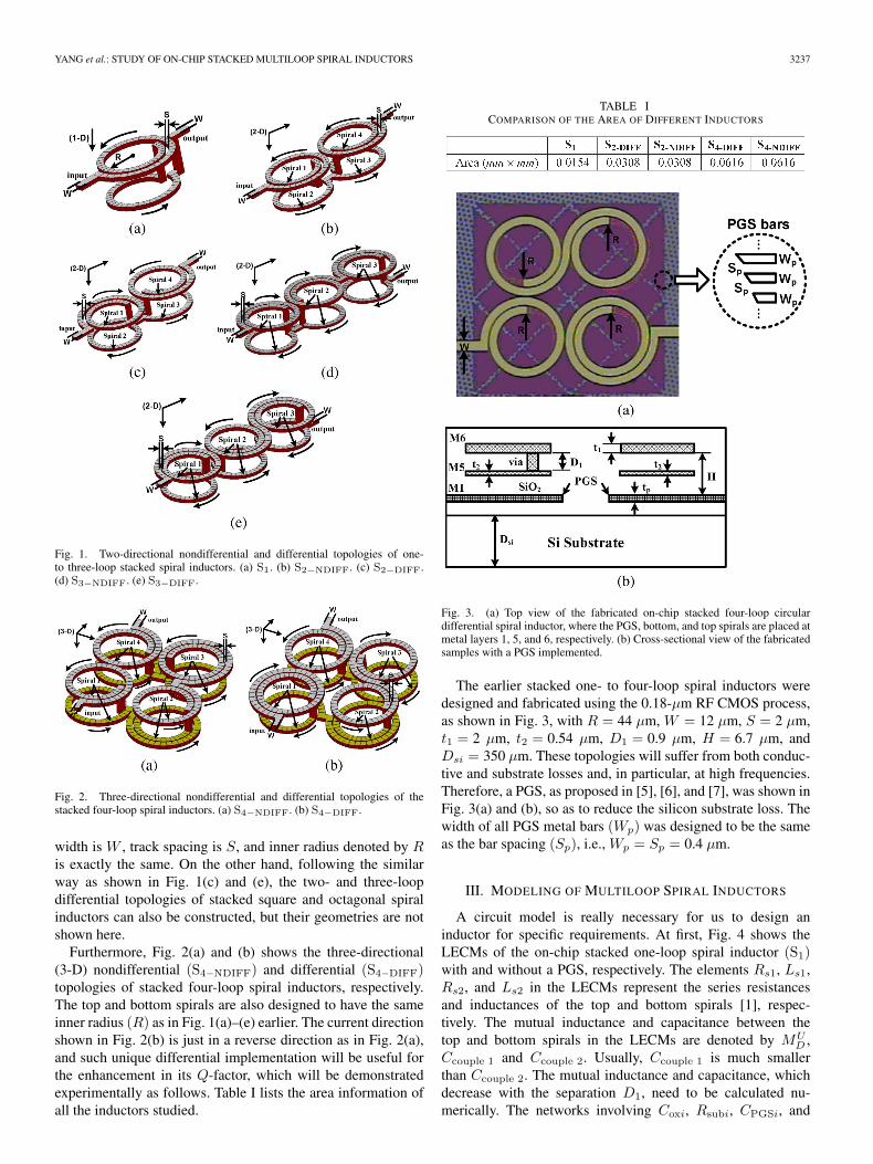
Fig. 3. (a) Top view of the fabricated on-chip stacked four-loop circulardifferential spiral inductor, where the PGS, bottom, and top spirals are placed atmetal layers 1, 5, and 6, respectively. (b) Cross-sectional view of the fabricatedsamples with a PGS implemented.
The earlier stacked one- to four-loop spiral inductors weredesigned and fabricated using the 0.18-μm RF CMOS process,as shown in Fig. 3, with R = 44 μm, W = 12 μm, S = 2 μm,t1 = 2 μm, t2 = 0.54 μm, D1 = 0.9 μm, H = 6.7 μm, andDsi = 350 μm. These topologies will suffer from both conduc-tive and substrate losses and, in particular, at high frequencies.Therefore, a PGS, as proposed in [5], [6], and [7], was shown inFig. 3(a) and (b), so as to reduce the silicon substrate loss. Thewidth of all PGS metal bars (Wp) was designed to be the sameas the bar spacing (Sp), i.e., Wp = Sp = 0.4 μm.
III. MODELING OF MULTILOOP SPIRAL INDUCTORS
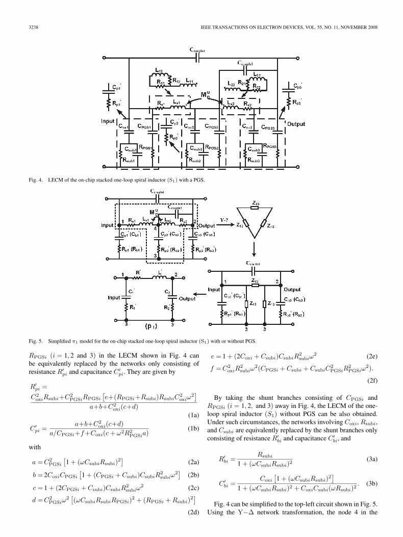
A circuit model is really necessary for us to design aninductor for specific requirements. At first, Fig. 4 shows theLECMs of the on-chip stacked one-loop spiral inductor (S1)with and without a PGS, respectively. The elements Rs1, Ls1,Rs2, and Ls2 in the LECMs represent the series resistancesand inductances of the top and bottom spirals [1], respec-tively. The mutual inductance and capacitance between thetop and bottom spirals in the LECMs are denoted by MU
D ,Ccouple 1 and Ccouple 2. Usually, Ccouple 1 is much smallerthan Ccouple 2. The mutual inductance and capacitance, whichdecrease with the separation D1, need to be calculated nu-merically. The networks involving Coxi, Rsubi, CPGSi, and
3238 IEEE TRANSACTIONS ON ELECTRON DEVICES, VOL. 55, NO. 11, NOVEMBER 2008
Fig. 4. LECM of the on-chip stacked one-loop spiral inductor (S1) with a PGS.
Fig. 5. Simplified π1 model for the on-chip stacked one-loop spiral inductor (S1) with or without PGS.
RPGSi (i = 1, 2 and 3) in the LECM shown in Fig. 4 canbe equivalently replaced by the networks only consisting ofresistance R′
pi and capacitance C ′pi. They are given by
R′pi =
C2oxiRsubi+C2
PGSiRPGSi
[e+(RPGSi+Rsubi)RsubiC
2oxiω
2]
a+b+C2oxi(c+d)
(1a)
C ′pi =
a+b+C2oxi(c+d)
a/CPGSi+f+Coxi(c + ω2R2PGSia)
(1b)
with
a = C2PGSi
[1 + (ωCsubiRsubi)2
](2a)
b = 2CoxiCPGSi
[1 + (CPGSi + Csubi)CsubiR
2subiω
2]
(2b)
c = 1 + (2CPGSi + Csubi)CsubiR2subiω
2 (2c)
d = C2PGSiω
2[(ωCsubiRsubiRPGSi)2 + (RPGSi + Rsubi)2
](2d)
e = 1 + (2Coxi + Csubi)CsubiR2subiω
2 (2e)
f =C2oxiR
2subiω
2(CPGSi + Csubi + CsubiC2PGSiR
2PGSiω
2).
(2f)
By taking the shunt branches consisting of CPGSi andRPGSi (i = 1, 2, and 3) away in Fig. 4, the LECM of the one-loop spiral inductor (S1) without PGS can be also obtained.Under such circumstances, the networks involving Coxi, Rsubi,and Csubi are equivalently replaced by the shunt branches onlyconsisting of resistance R′
bi and capacitance C ′bi, and
R′bi =
Rsubi
1 + (ωCsubiRsubi)2(3a)
C ′bi =
Coxi
[1 + (ωCsubiRsubi)2
]1 + (ωCsubiRsubi)2 + CoxiCsubi(ωRsubi)2
. (3b)
Fig. 4 can be simplified to the top-left circuit shown in Fig. 5.Using the Y−Δ network transformation, the node 4 in the
YANG et al.: STUDY OF ON-CHIP STACKED MULTILOOP SPIRAL INDUCTORS 3239
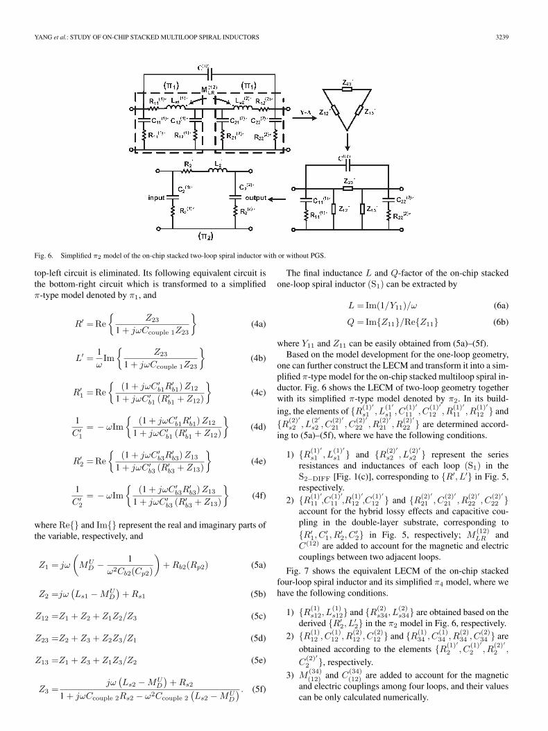
Fig. 6. Simplified π2 model of the on-chip stacked two-loop spiral inductor with or without PGS.
top-left circuit is eliminated. Its following equivalent circuit isthe bottom-right circuit which is transformed to a simplifiedπ-type model denoted by π1, and
R′ = Re{
Z23
1 + jωCcouple 1Z23
}(4a)
L′ =1ω
Im{
Z23
1 + jωCcouple 1Z23
}(4b)
R′1 = Re
{(1 + jωC ′
b1R′b1) Z12
1 + jωC ′b1 (R′
b1 + Z12)
}(4c)
1C ′
1
= − ωIm{
(1 + jωC ′b1R
′b1) Z12
1 + jωC ′b1 (R′
b1 + Z12)
}(4d)
R′2 = Re
{(1 + jωC ′
b3R′b3) Z13
1 + jωC ′b3 (R′
b3 + Z13)
}(4e)
1C ′
2
= − ωIm{
(1 + jωC ′b3R
′b3) Z13
1 + jωC ′b3 (R′
b3 + Z13)
}(4f)
where Re{} and Im{} represent the real and imaginary parts ofthe variable, respectively, and
Z1 = jω
(MU
D − 1ω2Cb2(Cp2)
)+ Rb2(Rp2) (5a)
Z2 =jω(Ls1 − MU
D
)+ Rs1 (5b)
Z12 =Z1 + Z2 + Z1Z2/Z3 (5c)
Z23 =Z2 + Z3 + Z2Z3/Z1 (5d)
Z13 =Z1 + Z3 + Z1Z3/Z2 (5e)
Z3 =jω
(Ls2 − MU
D
)+ Rs2
1 + jωCcouple 2Rs2 − ω2Ccouple 2
(Ls2 − MU
D
) . (5f)
The final inductance L and Q-factor of the on-chip stackedone-loop spiral inductor (S1) can be extracted by
L = Im(1/Y11)/ω (6a)
Q = Im{Z11}/Re{Z11} (6b)
where Y11 and Z11 can be easily obtained from (5a)–(5f).Based on the model development for the one-loop geometry,
one can further construct the LECM and transform it into a sim-plified π-type model for the on-chip stacked multiloop spiral in-ductor. Fig. 6 shows the LECM of two-loop geometry togetherwith its simplified π-type model denoted by π2. In its build-ing, the elements of {R(1)′
s1 , L(1′
s1 , C(1)′
11 , C(1)′
12 , R(1)′
11 , R(1)′
12 } and
{R(2)′
s2 , L(2′
s2 , C(2)′
21 , C(2)′
22 , R(2)′
21 , R(2)′
22 } are determined accord-ing to (5a)–(5f), where we have the following conditions.
1) {R(1)′
s1 , L(1)′
s1 } and {R(2)′
s2 , L(2)′
s2 } represent the seriesresistances and inductances of each loop (S1) in theS2−DIFF [Fig. 1(c)], corresponding to {R′, L′} in Fig. 5,respectively.
2) {R(1)′
11 ,C(1)′
11 ,R(1)′
12 ,C(1)′
12 } and {R(2)′
21 , C(2)′
21 , R(2)′
22 , C(2)′
22 }account for the hybrid lossy effects and capacitive cou-pling in the double-layer substrate, corresponding to{R′
1, C′1, R
′2, C
′2} in Fig. 5, respectively; M
(12)LR and
C(12) are added to account for the magnetic and electriccouplings between two adjacent loops.
Fig. 7 shows the equivalent LECM of the on-chip stackedfour-loop spiral inductor and its simplified π4 model, where wehave the following conditions.
1) {R(1)s12, L
(1)s12} and {R(2)
s34, L(2)s34} are obtained based on the
derived {R′2, L
′2} in the π2 model in Fig. 6, respectively.
2) {R(1)12 , C
(1)12 , R
(2)12 , C
(2)12 } and {R(1)
34 , C(1)34 , R
(2)34 , C
(2)34 } are
obtained according to the elements {R(1)′
2 , C(1)′
2 , R(2)′
2 ,
C(2)′
2 }, respectively.
3) M(34)(12) and C
(34)(12) are added to account for the magnetic
and electric couplings among four loops, and their valuescan be only calculated numerically.
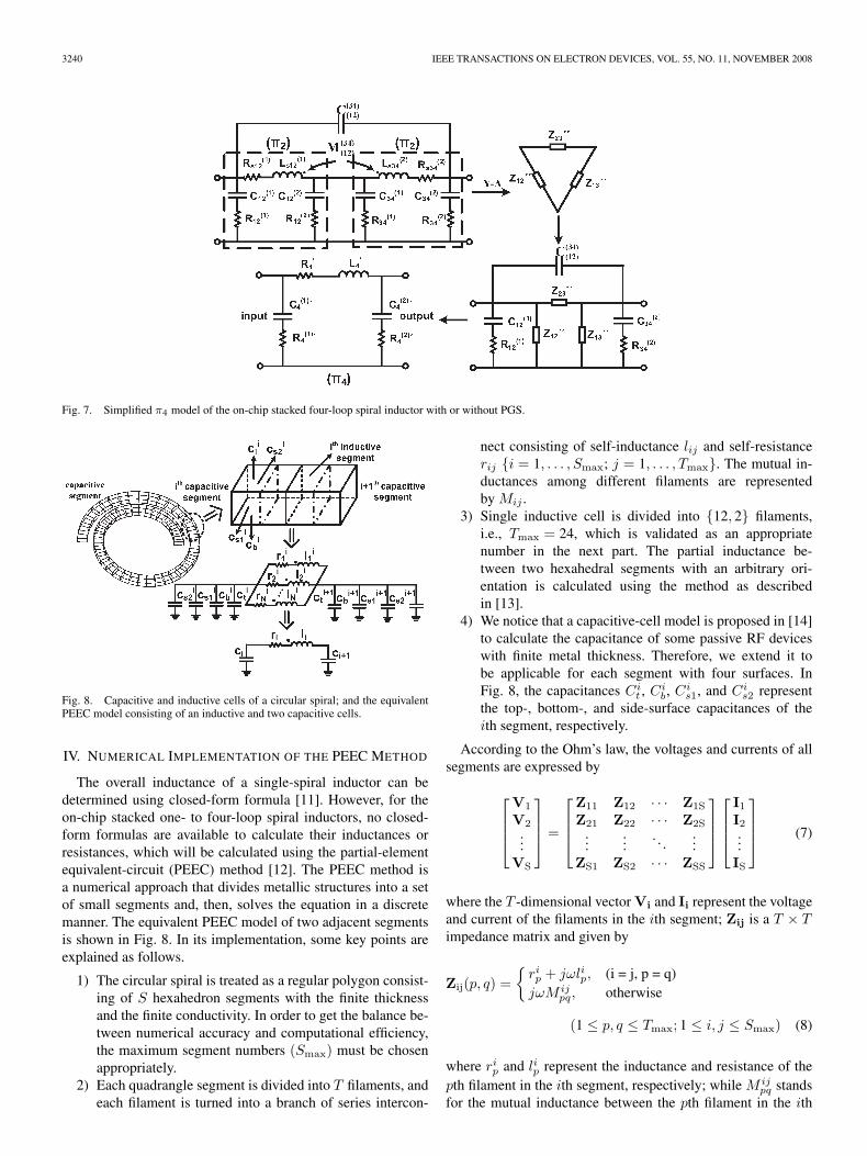
3240 IEEE TRANSACTIONS ON ELECTRON DEVICES, VOL. 55, NO. 11, NOVEMBER 2008
Fig. 7. Simplified π4 model of the on-chip stacked four-loop spiral inductor with or without PGS.
Fig. 8. Capacitive and inductive cells of a circular spiral; and the equivalentPEEC model consisting of an inductive and two capacitive cells.
IV. NUMERICAL IMPLEMENTATION OF THE PEEC METHOD
The overall inductance of a single-spiral inductor can bedetermined using closed-form formula [11]. However, for theon-chip stacked one- to four-loop spiral inductors, no closed-form formulas are available to calculate their inductances orresistances, which will be calculated using the partial-elementequivalent-circuit (PEEC) method [12]. The PEEC method isa numerical approach that divides metallic structures into a setof small segments and, then, solves the equation in a discretemanner. The equivalent PEEC model of two adjacent segmentsis shown in Fig. 8. In its implementation, some key points areexplained as follows.
1) The circular spiral is treated as a regular polygon consist-ing of S hexahedron segments with the finite thicknessand the finite conductivity. In order to get the balance be-tween numerical accuracy and computational efficiency,the maximum segment numbers (Smax) must be chosenappropriately.
2) Each quadrangle segment is divided into T filaments, andeach filament is turned into a branch of series intercon-
nect consisting of self-inductance lij and self-resistancerij {i = 1, . . . , Smax; j = 1, . . . , Tmax}. The mutual in-ductances among different filaments are representedby Mij .
3) Single inductive cell is divided into {12, 2} filaments,i.e., Tmax = 24, which is validated as an appropriatenumber in the next part. The partial inductance be-tween two hexahedral segments with an arbitrary ori-entation is calculated using the method as describedin [13].
4) We notice that a capacitive-cell model is proposed in [14]to calculate the capacitance of some passive RF deviceswith finite metal thickness. Therefore, we extend it tobe applicable for each segment with four surfaces. InFig. 8, the capacitances Ci
t , Cib, Ci
s1, and Cis2 represent
the top-, bottom-, and side-surface capacitances of theith segment, respectively.
According to the Ohm’s law, the voltages and currents of allsegments are expressed by
⎡⎢⎢⎣
V1
V2...
VS
⎤⎥⎥⎦ =
⎡⎢⎢⎣
Z11 Z12 · · · Z1S
Z21 Z22 · · · Z2S...
.... . .
...ZS1 ZS2 · · · ZSS
⎤⎥⎥⎦
⎡⎢⎢⎣
I1
I2...IS
⎤⎥⎥⎦ (7)
where the T -dimensional vector Vi and Ii represent the voltageand current of the filaments in the ith segment; Zij is a T × Timpedance matrix and given by
Zij(p, q) ={
rip + jωlip, (i = j, p = q)
jωM ijpq, otherwise
(1 ≤ p, q ≤ Tmax; 1 ≤ i, j ≤ Smax) (8)
where rip and lip represent the inductance and resistance of the
pth filament in the ith segment, respectively; while M ijpq stands
for the mutual inductance between the pth filament in the ith
YANG et al.: STUDY OF ON-CHIP STACKED MULTILOOP SPIRAL INDUCTORS 3241
segment and the qth filament in the jth segment. Equation (7)can be converted into
⎡⎢⎢⎣
I1
I2...IS
⎤⎥⎥⎦ =
⎡⎢⎢⎣
Z11 Z12 · · · Z1S
Z21 Z22 · · · Z2S...
.... . .
...ZS1 ZS2 · · · ZSS
⎤⎥⎥⎦−1 ⎡
⎢⎢⎣V1
V2...
VS
⎤⎥⎥⎦
≡
⎡⎢⎢⎣
Y11 Y12 · · · Y1S
Y21 Y22 · · · Y2S...
.... . .
...YS1 YS2 · · · YSS
⎤⎥⎥⎦
⎡⎢⎢⎣
V1
V2...
VS
⎤⎥⎥⎦ . (9)
For each branch, we have
Vi =Vi(p) (10a)
Ii =Tmax∑p=1
Ii(p) (10b)
where Vi and Ii denote the voltage and current of the ithsegment, respectively. Therefore, we further have
⎡⎢⎢⎣
I1
I2...
IS
⎤⎥⎥⎦ =
⎡⎢⎢⎣
Y11 Y12 · · · Y1S
Y21 Y22 · · · Y2S...
.... . .
...YS1 YS2 · · · YSS
⎤⎥⎥⎦
⎡⎢⎢⎣
V1
V2...
VS
⎤⎥⎥⎦ (11)
Yij =Tmax∑p=1
Tmax∑q=1
Yij(p, q). (12)
From (11), we can obtain all elements in the [Z]-matrix. Theseries resistance and inductance are thus calculated by
Rs =Re
⎧⎨⎩
Smax∑i=1
Smax∑j=1
Zij
⎫⎬⎭ (13a)
Ls =1ω
Im
⎧⎨⎩
Smax∑i=1
Smax∑j=1
Zij
⎫⎬⎭ . (13b)
The mutual inductive coupling plays an important role in theenhancement of the total inductance earlier. Taking the four-loop geometry as an example, each spiral is divided into Smax
segments. Thus, the mutual inductance between spirals p andq (p, q = 1, 2, 3, 4, and p �= q) can be calculated by
Mpq =1ω
Im
⎧⎨⎩
pSmax∑i=1+(p−1)Smax
qSmax∑j=1+(q−1)Smax
Zij
⎫⎬⎭ . (14)
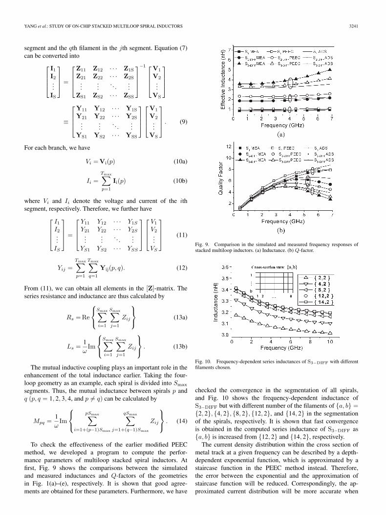
To check the effectiveness of the earlier modified PEECmethod, we developed a program to compute the perfor-mance parameters of multiloop stacked spiral inductors. Atfirst, Fig. 9 shows the comparisons between the simulatedand measured inductances and Q-factors of the geometriesin Fig. 1(a)–(e), respectively. It is shown that good agree-ments are obtained for these parameters. Furthermore, we have
Fig. 9. Comparison in the simulated and measured frequency responses ofstacked multiloop inductors. (a) Inductance. (b) Q-factor.
Fig. 10. Frequency-dependent series inductances of S3−DIFF with differentfilaments chosen.
checked the convergence in the segmentation of all spirals,and Fig. 10 shows the frequency-dependent inductance ofS3−DIFF but with different number of the filaments of {a, b} ={2, 2}, {4, 2}, {8, 2}, {12, 2}, and {14, 2} in the segmentationof the spirals, respectively. It is shown that fast convergenceis obtained in the computed series inductance of S3−DIFF as{a, b} is increased from {12, 2} and {14, 2}, respectively.
The current density distribution within the cross section ofmetal track at a given frequency can be described by a depth-dependent exponential function, which is approximated by astaircase function in the PEEC method instead. Therefore,the error between the exponential and the approximation ofstaircase function will be reduced. Correspondingly, the ap-proximated current distribution will be more accurate when
3242 IEEE TRANSACTIONS ON ELECTRON DEVICES, VOL. 55, NO. 11, NOVEMBER 2008
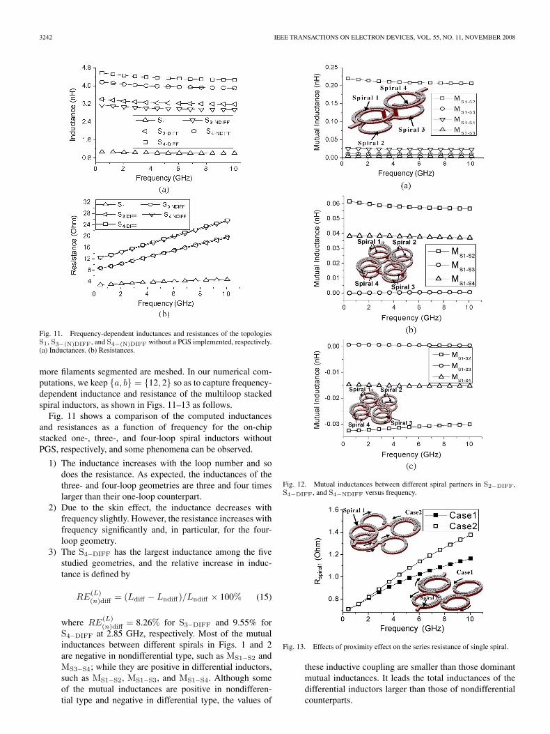
Fig. 11. Frequency-dependent inductances and resistances of the topologiesS1, S3−(N)DIFF, and S4−(N)DIFF without a PGS implemented, respectively.(a) Inductances. (b) Resistances.
more filaments segmented are meshed. In our numerical com-putations, we keep {a, b} = {12, 2} so as to capture frequency-dependent inductance and resistance of the multiloop stackedspiral inductors, as shown in Figs. 11–13 as follows.
Fig. 11 shows a comparison of the computed inductancesand resistances as a function of frequency for the on-chipstacked one-, three-, and four-loop spiral inductors withoutPGS, respectively, and some phenomena can be observed.
1) The inductance increases with the loop number and sodoes the resistance. As expected, the inductances of thethree- and four-loop geometries are three and four timeslarger than their one-loop counterpart.
2) Due to the skin effect, the inductance decreases withfrequency slightly. However, the resistance increases withfrequency significantly and, in particular, for the four-loop geometry.
3) The S4−DIFF has the largest inductance among the fivestudied geometries, and the relative increase in induc-tance is defined by
RE(L)(n)diff = (Ldiff − Lndiff)/Lndiff × 100% (15)
where RE(L)(n)diff = 8.26% for S3−DIFF and 9.55% for
S4−DIFF at 2.85 GHz, respectively. Most of the mutualinductances between different spirals in Figs. 1 and 2are negative in nondifferential type, such as MS1−S2 andMS3−S4; while they are positive in differential inductors,such as MS1−S2, MS1−S3, and MS1−S4. Although someof the mutual inductances are positive in nondifferen-tial type and negative in differential type, the values of
Fig. 12. Mutual inductances between different spiral partners in S2−DIFF,S4−DIFF, and S4−NDIFF versus frequency.
Fig. 13. Effects of proximity effect on the series resistance of single spiral.
these inductive coupling are smaller than those dominantmutual inductances. It leads the total inductances of thedifferential inductors larger than those of nondifferentialcounterparts.
YANG et al.: STUDY OF ON-CHIP STACKED MULTILOOP SPIRAL INDUCTORS 3243
Fig. 14. Experimentally extracted equivalent inductance as a function of
frequency for topologies of S(PGS)4−DIFF and S
(NPGS)4−NDIFF.
4) There is very little difference in the computed resistancebetween S3−DIFF and S3−NDIFF or between S4−DIFF
and S4−NDIFF over a wide frequency range, because theoverall metal-track length in the differential topology isnearly the same as that in its nondifferential counterpart.
Fig. 12(a) and (b) shows the computed mutual inductancesbetween different spiral partners in S2−DIFF and S4−DIFF,respectively, where MSi−Sj represents the mutual inductancebetween the spirals (i = 1 and 2) and (j = 3 and 4), as shownin Fig. 12. It is obvious that the mutual inductance betweenspirals one and two is much larger than those of other cases[Fig. 12(a)].
Fig. 13 shows the proximity effects on the frequency-dependent series resistance of single spiral denoted by Spiral 1with neighborhoods of three spirals in Case 1 and four spirals inCase 2, respectively. The spirals are not physically connected inthe inlets in Fig. 13. The arrows represent the fictitious currentdirection which are independent in different spirals.
It is evident that proximity effects on the series resistancecannot be excluded at high frequencies, and the relative increasein series resistance between Cases 1 and 2 is defined by
RER = (Rcase 2 − Rcase 1)/Rcase 1 × 100% (16)
where RER = 9.15% at f = 4.85 GHz and 18.39% at f =10.05 GHz approximately. With the increase in frequency, theproximity effect on the series resistance in Case 2 will be muchmore significant than that in Case 1. The main reason is that themutual magnetic coupling between the vertically neighboringspirals is much larger than that between the laterally neigh-boring spirals. In Fig. 12(a), the mutual inductance betweenvertically neighboring spirals MS1−S2 is around ten times largerthan those between lateral neighboring spirals, such as MS1−S4
and MS2−S3 in all frequencies. The more significant the mutualinductive coupling is, the more dominant the proximity effectwill be.
V. EXPERIMENTAL RESULTS AND DISCUSSIONS
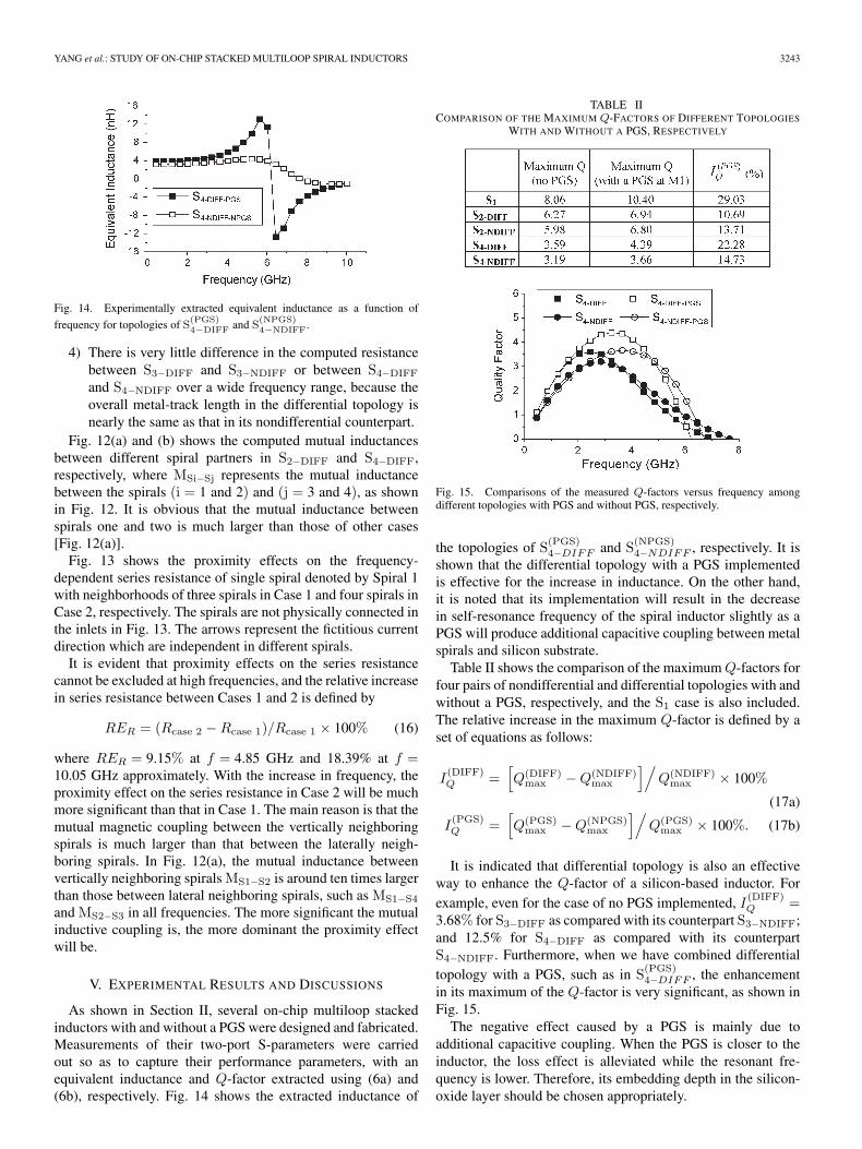
As shown in Section II, several on-chip multiloop stackedinductors with and without a PGS were designed and fabricated.Measurements of their two-port S-parameters were carriedout so as to capture their performance parameters, with anequivalent inductance and Q-factor extracted using (6a) and(6b), respectively. Fig. 14 shows the extracted inductance of
TABLE IICOMPARISON OF THE MAXIMUM Q-FACTORS OF DIFFERENT TOPOLOGIES
WITH AND WITHOUT A PGS, RESPECTIVELY
Fig. 15. Comparisons of the measured Q-factors versus frequency amongdifferent topologies with PGS and without PGS, respectively.
the topologies of S(PGS)4−DIFF and S(NPGS)
4−NDIFF , respectively. It isshown that the differential topology with a PGS implementedis effective for the increase in inductance. On the other hand,it is noted that its implementation will result in the decreasein self-resonance frequency of the spiral inductor slightly as aPGS will produce additional capacitive coupling between metalspirals and silicon substrate.
Table II shows the comparison of the maximum Q-factors forfour pairs of nondifferential and differential topologies with andwithout a PGS, respectively, and the S1 case is also included.The relative increase in the maximum Q-factor is defined by aset of equations as follows:
I(DIFF)Q =
[Q(DIFF)
max − Q(NDIFF)max
]/Q(NDIFF)
max × 100%
(17a)
I(PGS)Q =
[Q(PGS)
max − Q(NPGS)max
]/Q(PGS)
max × 100%. (17b)
It is indicated that differential topology is also an effectiveway to enhance the Q-factor of a silicon-based inductor. Forexample, even for the case of no PGS implemented, I
(DIFF)Q =
3.68% for S3−DIFF as compared with its counterpart S3−NDIFF;and 12.5% for S4−DIFF as compared with its counterpartS4−NDIFF. Furthermore, when we have combined differentialtopology with a PGS, such as in S(PGS)
4−DIFF , the enhancementin its maximum of the Q-factor is very significant, as shown inFig. 15.
The negative effect caused by a PGS is mainly due toadditional capacitive coupling. When the PGS is closer to theinductor, the loss effect is alleviated while the resonant fre-quency is lower. Therefore, its embedding depth in the silicon-oxide layer should be chosen appropriately.
3244 IEEE TRANSACTIONS ON ELECTRON DEVICES, VOL. 55, NO. 11, NOVEMBER 2008
VI. CONCLUSION
New differential multiloop topologies that features stackedstructure were proposed first. A comparative study on one- tofour-loop inductors with and without PGSs were conductedin this paper. To handle these multiloop stacked configu-rations, LECMs were developed for enhancing our analy-sis. Furthermore, PEEC method was employed for predictingthe frequency-dependent inductances and resistances of theseinductors. Good agreements between numerical results andon-chip measurements were observed. They showed that adifferential multiloop stacked spiral inductor with a PGS canincrease the inductance and Q-factor significantly and only re-duce self-resonant frequency slightly. Therefore, the proposeddifferential multiloop stacked spiral inductors are very suitablefor the design of RFICs with high quality.
REFERENCES
[1] Y. Cao, R. A. Groves, N. D. Zamdmer, J. O. Plouchart, R. A. Wachnik,X. J. Huang, T. J. King, and C. M. Hu, “Frequency-independentequivalent-circuit model for on-chip spiral inductors,” IEEE J. Solid-StateCircuits, vol. 38, no. 3, pp. 743–752, Mar. 2003.
[2] F. Rotella, B. K. Bhattacharya, V. Blaschke, M. Matloubian, A. Brotman,Y. H. Cheng, R. Divecha, D. Howard, K. Lampaert, P. Miliozzi,M. Racanelli, P. Singh, and P. J. Zampardi, “A broad-band lumped elementanalytic model incorporating skin effect and substrate loss for inductorsand inductor like components for silicon technology performance assess-ment and RFIC design,” IEEE Trans. Electron Devices, vol. 52, no. 7,pp. 1429–1441, Jul. 2005.
[3] A. M. Niknejad and R. G. Meyer, “Analysis of eddy current losses overconductive substrates with applications to monolithic inductors and trans-formers,” IEEE Trans. Microw. Theory Tech., vol. 49, no. 1, pp. 166–176,Jan. 2001.
[4] J. Chen and J. J. Liu, “Modeling of on-chip differential inductors andtransformers/baluns,” IEEE Trans. Electron Devices, vol. 54, no. 2,pp. 369–371, Feb. 2007.
[5] C. P. Yue and S. S. Wong, “On-chip spiral inductors with patterned groundshields for Si-based RFICs,” IEEE J. Solid-State Circuits, vol. 33, no. 5,pp. 743–752, May 1998.
[6] C. A. Chang, S. P. Tseng, J. Y. Chung, S. S. Jiang, and J. A. Yeh,“Characterization of spiral inductors with patterned floating structures,”IEEE Trans. Microw. Theory Tech., vol. 52, no. 5, pp. 1375–1381,May 2004.
[7] T. S. D. Cheung and J. R. Long, “Shielded passive device forsilicon-based monolithic microwave and millimeter-wave integrated cir-cuits,” IEEE J. Solid-State Circuits, vol. 41, no. 5, pp. 1183–1200,May 2006.
[8] A. Zolfaghari, A. Chan, and B. Razavi, “Stacked inductors and transform-ers in CMOS technology,” IEEE J. Solid-State Circuits, vol. 36, no. 4,pp. 620–628, Apr. 2001.
[9] C.-C. Tang, C.-H. Wu, and S.-I. Liu, “Miniature 3-D inductors in standardCMOS process,” IEEE J. Solid-State Circuits, vol. 37, no. 4, pp. 471–479,Apr. 2002.
[10] W. Y. Yin, S. J. Pan, L. W. Li, and Y. B. Gan, “Modeling on-chip circu-lar double-spiral stacked inductors for RFICs,” Proc. Inst. Elect. Eng.—Microw., Antennas Propag., vol. 150, no. 6, pp. 463–469, Dec. 2003.
[11] J. Kuo, K.-Y. Su, T.-Y. Liu, H.-H. Chen, and S.-J. Chung, “Analyticalcalculation for DC inductances of rectangular spiral inductors with finitemetal thickness in the PEEC formulation,” IEEE Microw. Wireless Com-pon. Lett., vol. 16, no. 2, pp. 69–71, Feb. 2006.
[12] A. E. Ruehli, “Equivalent circuit models for three-dimensional multi-conductor systems,” IEEE Trans. Microw. Theory Tech., vol. MTT-22,no. 3, pp. 216–221, Mar. 1974.
[13] D. R. Wilton, S. Rao, A. Glisson, D. Schaubert, O. Al-bundrak, andC. Butler, “Potential integrals for uniform and linear source distributionson polygonal and polyhedral domains,” IEEE Trans. Antennas Propag.,vol. AP-32, no. 3, pp. 276–281, Mar. 1984.
[14] K. L. Wu, L. K. Yeung, and Y. Ding, “An efficient PEEC algorithmfor modeling of LTCC RF circuits with finite metal strip thickness,”IEEE Microw. Wireless Compon. Lett., vol. 13, no. 9, pp. 390–392,Sep. 2003.
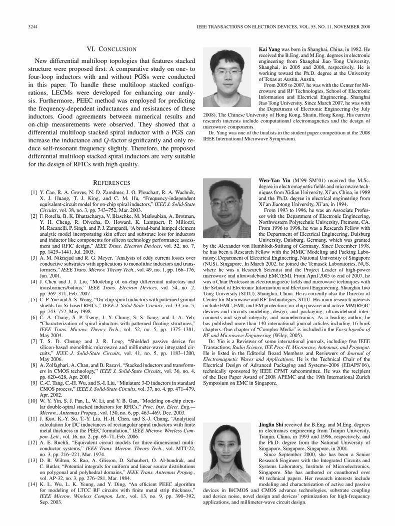
Kai Yang was born in Shanghai, China, in 1982. Hereceived the B.Eng. and M.Eng. degrees in electronicengineering from Shanghai Jiao Tong University,Shanghai, in 2005 and 2008, respectively. He isworking toward the Ph.D. degree at the Universityof Texas at Austin, Austin.
From 2005 to 2007, he was with the Center for Mi-crowave and RF Technologies, School of ElectronicInformation and Electrical Engineering, ShanghaiJiao Tong University. Since March 2007, he was withthe Department of Electronic Engineering (by July
2008), The Chinese University of Hong Kong, Shatin, Hong Kong. His currentresearch interests include computational electromagnetics and the design ofmicrowave components.
Dr. Yang was one of the finalists in the student paper competition at the 2008IEEE International Microwave Symposium.
Wen-Yan Yin (M’99–SM’01) received the M.Sc.degree in electromagnetic fields and microwave tech-niques from Xidian University, Xi’an, China, in 1989and the Ph.D. degree in electrical engineering fromXi’an Jiaotong University, Xi’an, in 1994.
From 1993 to 1996, he was an Associate Profes-sor with the Department of Electronic Engineering,Northwestern Polytechnic University, Fremont, CA.From 1996 to 1998, he was a Research Fellow withthe Department of Electrical Engineering, DuisburgUniversity, Duisburg, Germany, which was granted
by the Alexander von Humblodt-Stiftung of Germany. Since December 1998,he has been a Research Fellow with the MMIC Modeling and Packing Labo-ratory, Department of Electrical Engineering, National University of Singapore(NUS), Singapore. In March 2002, he joined the Temasek Laboratories, NUS,where he was a Research Scientist and the Project Leader of high-powermicrowave and ultrawideband EMC/EMI. From April 2005 to end of 2007, hewas a Chair Professor in electromagnetic fields and microwave techniques withthe School of Electronic Information and Electrical Engineering, Shanghai JiaoTong University (SJTU), Shanghai, China. He is currently also the Director ofCenter for Microwave and RF Technologies, SJTU. His main research interestsinclude EMC, EMI, and EM protection; on-chip passive and active MM(RF)ICdevices and circuits modeling, design, and packaging; ultrawideband inter-connects and signal integrity; and nanoelectronics. As a leading author, hehas published more than 140 international journal articles including 16 bookchapters. One chapter of “Complex Media” is included in the Encyclopedia ofRF and Microwave Engineering (Wiley, 2005).
Dr. Yin is a Reviewer of some international journals, including five IEEETransactions, Radio Science, IEE Proc-H, Microwave, Antennas, and Propagat.He is listed in the Editorial Board Members and Reviewers of Journal ofElectromagnetic Waves and Applications. He is the Technical Chair of theElectrical Design of Advanced Packaging and Systems–2006 (EDAPS’06),technically sponsored by IEEE CPMT subcommittee. He was the recipientof the Best Paper Award of 2008 APEMC and the 19th International ZurichSymposium on EMC in Singapore.
Jinglin Shi received the B.Eng. and M.Eng. degreesin electronics engineering from Tianjin University,Tianjin, China, in 1993 and 1996, respectively, andthe Ph.D. degree from the National University ofSingapore, Singapore, Singapore, in 2001.
Since September 2000, she has been a SeniorResearch Engineer with the Integrated Circuits andSystems Laboratory, Institute of Microelectronics,Singapore. She has authored or coauthored over40 technical papers. Her research interests includemodeling and characterization of active and passive
devices in BiCMOS and CMOS advance technologies, substrate couplingand device noise, novel design and devices’ optimization for high-frequencyapplications, and millimeter-wave circuit design.
YANG et al.: STUDY OF ON-CHIP STACKED MULTILOOP SPIRAL INDUCTORS 3245
Kai Kang received the B.Eng. degree in electricalengineering from the Northwestern PolytechnicalUniversity, Xi’an of China, in 2002 and the jointPh.D. degree from the National University ofSingapore, Singapore, and Ecole SupérieureD’électricité, Gif-sur-Yvette, France, in 2008.
Since 2003, he has been a Research Scholar withthe National University of Singapore. From 2005 to2006, he was with the Laboratoire de Génie Elec-trique de Paris, Paris, France. Since October 2006,he has been a Senior Research Engineer with the
Institute of Microelectronics, Singapore. His research interest includes mod-eling of on-chip passive devices and millimeter-wave circuit design in CMOStechnology.
Jun-Fa Mao (M’92–SM’98) was born in 1965. Hereceived the B.S. degree from the University ofScience and Technology of National Defense,Changsha of China, in 1985, the M.S. degree fromthe Shanghai Institute of Nuclear Research, Acad-emic Sinica, Shanghai of China, in 1988, and thePh.D. degree from Shanghai Jiao Tong University,Shanghai, China, in 1992.
Since 1992, he has been a Faculty Member withthe Department of Electronic Engineering, ShanghaiJiao Tong University, where he is currently a Profes-
sor. From 1994 to 1995, he was a Visiting Scholar at the Chinese Universityof Hong Kong, Shatin, Hong Kong. From 1995 to 1996, he was a PostdoctoralResearcher with the University of California, Berkeley. He was an AssociateDean with the School of Electronic, Information and Electrical Engineering,Shanghai Jiao Tong University, from 1999 to 2005. He was a Topic Expert ofthe High-Tech Program of China from 2001 to 2003. He has published morethan 200 papers and a coauthored book. His research interests include theinterconnect problem of high-speed integrated circuits and novel microwavecomponents and circuits.
Dr. Mao was the recipient of the Second-Class National Natural ScienceAward of China in 2004 and the First-Class Natural Science Award of Shanghai,in 2005. He is a Cheung Kong Scholar of the Ministry of Education, China,an Associate Director of the China Institute of Electronics on MicrowaveSociety, and the 2007–2008 Chair of IEEE Shanghai Section. He is a CheungKong Scholar of the Ministry of Education, China, the Associate Chair ofthe Microwave Society of China, the Chair of IEEE Shanghai Subsectionfor 2004 and 2005, and the General Chair of Electrical Design of AdvancedPackaging and Systems–2006 (EDAPS’06), technically sponsored by IEEECPMT Subcommittee.
Y. P. Zhang received the B.E. degree in electronicengineering from the Taiyuan Polytechnic Institute,Taiyuan University of Technology, Shanxi, China, in1982, the M.E. degree in electronic engineering fromthe Shanxi Mining Institute, Taiyuan University ofTechnology, Shanxi, in 1987, and the Ph.D. degree inelectronic engineering from the Chinese Universityof Hong Kong, Shatin, Hong Kong, in 1995.
From 1982 to 1984, he was with the ShanxiElectronic Industry Bureau. From 1987 to 1990, hewas with the Shanxi Mining Institute. From 1990 to
1992, he was with the University of Liverpool, Liverpool, U.K. From 1996to 1997, he was with the City University of Hong Kong, Kowloon, HongKong. In 1996, he was a Full Professor with Taiyuan University of Technology.From 1997 to 1998, he was with the University of Hong Kong, Hong Kong.He is currently an Associate Professor and the Deputy Supervisor of theIntegrated Circuits and Systems Laboratories with the School of Electrical andElectronic Engineering, Nanyang Technological University, Singapore. He hasbroad interests in radio science and technology and published widely acrossseven IEEE societies. He has delivered scores of invited papers/keynote addressat international scientific conferences.
Dr. Zhang was the recipient of the Sino-British Technical CollaborationAward in 1990 for his contribution to the advancement of subsurface radioscience and technology. He was the recipient of the Best Paper Award from theSecond IEEE International Symposium on Communication Systems, Networksand Digital Signal Processing, July 18–20, 2000, Bournemouth, U.K., and theBest Paper Prize from the Third IEEE International Workshop on AntennaTechnology, March 21–23, 2007, Cambridge, U.K. He was the recipient of aWilliam Mong Visiting Fellowship from the University of Hong Kong in 2005.He is listed in Marquis Who’s Who, Who’s Who in Science and Engineering,Cambridge IBC 2000 Outstanding Scientists of the 21st Century. He serveson the Editorial Board of the International Journal of RF and MicrowaveComputer-Aided Engineering and was a Guest Editor of the journal for theSpecial Issue RF and Microwave Subsystem Modules for Wireless Communica-tions. He also serves as an Associate Editor of the International Journal of Mi-crowave Science and Technology and an Associate Editor of the InternationalJournal of Electromagnetic Waves and Applications. Furthermore, he serves onthe Editorial Boards of the IEEE TRANSACTIONS ON MICROWAVE THEORY
AND TECHNIQUES and IEEE MICROWAVE AND WIRELESS COMPONENTS
LETTERS.