Embed Size (px)
Citation preview

Reproduced with permission of the copyright owner. Further reproduction prohibited without permission.
A study of the loop as a compact antennaLea, AndrewProQuest Dissertations and Theses; 2007; ProQuest Dissertations & Theses (PQDT)pg. n/a
A Study of the Loop as a Compact Antenna
by
Andrew Lea
B.Eng., Dalhousie University, 2004
A THESIS SUBMITTED IN PARTIAL FULFILLMENT OF
THE REQUIREMENTS FOR THE DEGREE OF
MASTER OF ApPLIED SCIENCE
in the School
of
Engineering Science
© Andrew Lea 2007
SIMON FRASER UNIVERSITY
2007
All rights reserved. This work may not be
reproduced in whole or in part, by photocopy
or other means, without permission of the author.

Reproduced with permission of the copyright owner. Further reproduction prohibited without permission.
1+1 Library and Archives Canada
Bibliotheque et Archives Canada
Published Heritage Branch
Direction du Patrimoine de I'edition
395 Wellington Street Ottawa ON K1A ON4 Canada
395, rue Wellington Ottawa ON K1A ON4 Canada
NOTICE: The author has granted a nonexclusive license allowing Library and Archives Canada to reproduce, publish, archive, preserve, conserve, communicate to the public by telecommunication or on the Internet, loan, distribute and sell theses worldwide, for commercial or noncommercial purposes, in microform, paper, electronic and/or any other formats.
The author retains copyright ownership and moral rights in this thesis. Neither the thesis nor substantial extracts from it may be printed or otherwise reproduced without the author's permission.
In compliance with the Canadian Privacy Act some supporting forms may have been removed from this thesis.
While these forms may be included in the document page count, their removal does not represent any loss of content from the thesis.
• •• Canada
AVIS:
Your file Votre reference ISBN: 978-0-494-40734-9 Our file Notre reference ISBN: 978-0-494-40734-9
L'auteur a accorde une licence non exclusive permettant a la Bibliotheque et Archives Canada de reproduire, publier, archiver, sauvegarder, conserver, transmettre au public par telecommunication ou par l'lnternet, preter, distribuer et vendre des theses partout dans Ie monde, a des fins commerciales ou autres, sur support microforme, papier, electronique eUou autres formats.
L'auteur conserve la propriete du droit d'auteur et des droits moraux qui protege cette these. Ni la these ni des extraits substantiels de celle-ci ne doivent etre imprimes ou autrement reproduits sans son autorisation.
Conformement a la loi canadienne sur la protection de la vie privee, quelques formulaires secondaires ont ete enleves de cette these.
Bien que ces formulaires aient inclus dans la pagination, il n'y aura aucun contenu manquant.

Reproduced with permission of the copyright owner. Further reproduction prohibited without permission.
Name:
Degree:
Title of Thesis:
Examining Committee:
Date Approved:
Approval
Andrew Lea
Master of Applied Science
A Study of the Loop as a Compact Antenna
Dr. Paul Ho
Chair
Dr. Rodney Vaughan
Senior Supervisor
Dr. James K. Cavers
Supervisor
Dr. Nima Mahanfar
SFU Examiner
11

Reproduced with permission of the copyright owner. Further reproduction prohibited without permission.
SIMON FRASER UNIVERSITY LIBRARY
Declaration of Partial Copyright Licence
The author, whose copyright is declared on the title page of this work, has granted to Simon Fraser University the right to lend this thesis, project or extended essay to users of the Simon Fraser University Library, and to make partial or single copies only for such users or in response to a request from the library of any other university, or other educational institution, on its own behalf or for one of its users.
The author has further granted permission to Simon Fraser University to keep or make a digital copy for use in its circulating collection (currently available to the public at the "Institutional Repository" link of the SFU Library website <www.lib.sfu.ca> at: <http://ir.lib.sfu.ca/handle/1892/112>) and, without changing the content, to translate the thesis/project or extended essays, if technically possible, to any medium or format for the purpose of preservation of the digital work.
The author has further agreed that permission for multiple copying of this work for scholarly purposes may be granted by either the author or the Dean of Graduate Studies.
It is understood that copying or publication of this work for financial gain shall not be allowed without the author's written permission.
Permission for public performance, or limited permission for private scholarly use, of any multimedia materials forming part of this work, may have been granted by the author. This information may be found on the separately catalogued multimedia material and in the signed Partial Copyright Licence.
While licensing SFU to permit the above uses, the author retains copyright in the thesis, project or extended essays, including the right to change the work for subsequent purposes, including editing and publishing the work in whole or in part, and licensing other parties, as the author may desire.
The original Partial Copyright Licence attesting to these terms, and signed by this author, may be found in the original bound copy of this work, retained in the Simon Fraser University Archive.
Simon Fraser University Library Burnaby, BC,Canada
Revised: Summer 2007

Reproduced with permission of the copyright owner. Further reproduction prohibited without permission.
Abstract
This thesis examines the suitability of the loop antenna for use as a compact radiating
element. The derivation of the loop equation is reviewed, and a summary of the
significant research on the electrically large loop antenna over the past century is
presented. The theoretical radiation efficiency for the electrically large loop is derived.
This analysis shows that the radiation efficiency of the loop antenna is drastically
improved by increasing the electrical size of the loop. The theoretical input impedance is
used to calculate the quality factor and bandwidth of the tuned loop antenna, and a
suitable impedance matching technique is presented to attain this bandwidth. Several
loop antennas were constructed, and a Wheeler cap was used to measure the radiation
efficiency of these antennas. This measured radiation efficiency is shown to agree
reasonably well with the theoretically predicted values.
111

Reproduced with permission of the copyright owner. Further reproduction prohibited without permission.
Dedication
To my wife, Meghan, and father, James, both of whom asked everyday "when will the
thesis be finished?", and whom will never read beyond these first two pages.
IV

Reproduced with permission of the copyright owner. Further reproduction prohibited without permission.
Acknowledgements
A thank you to my senior supervisor, Dr. Rodney Vaughan, who always had time
to answer my questions, no matter what time of the day I knocked on his office door. I
would also like to thank Dr. Nima Mahanfar for his suggestions and input during the
latter part of this research.
v

Reproduced with permission of the copyright owner. Further reproduction prohibited without permission.
Contents
Approval ............................................................................................................................. ii
Abstract .............................................................................................................................. iii
Dedication .......................................................................................................................... iv
Acknowledgements ............................................................................................................. v
Contents ............................................................................................................................. vi
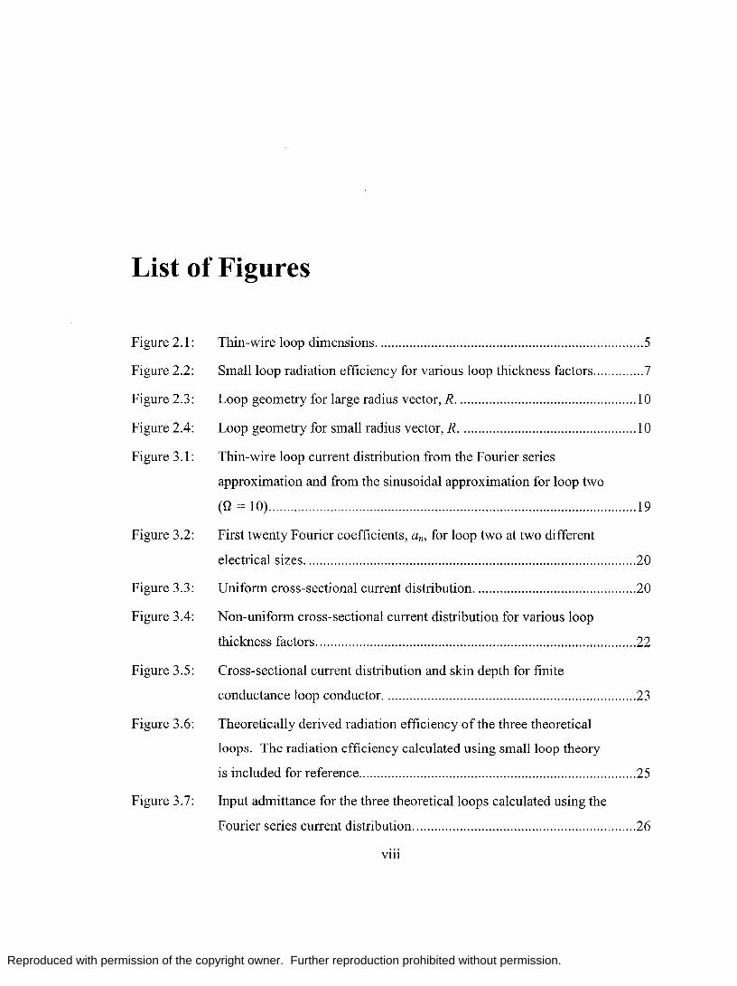
List of Figures .................................................................................................................. viii
List of Tables ................................................................................................................... xiii
1. Introduction ............................................................................................................. 1
2. Existing Theoretical Analysis ................................................................................. 4
2.1 Loop Antenna Dimensions ......................................................................... 4
2.2 Small Loop Theory ..................................................................................... 5
2.3 The Loop Equation ..................................................................................... 7
2.4 Solving the Loop Equation ....................................................................... 14
2.5 Radiation Fields ........................................................................................ 17
3. Theoretical Results ................................................................................................ 18
3.1 Current Distribution .................................................................................. 18
3.2 Radiation Efficiency ................................................................................. 22
3.3 Input Impedance ........................................................................................ 26
3.4 Quality Factor, Bandwidth, and Impedance Matching ............................. 28
4. Loop Measurements .............................................................................................. 37
4.1 Measured Impedances ............................................................................... 39
VI

Reproduced with permission of the copyright owner. Further reproduction prohibited without permission.
4.2 Radiation Efficiency Measurements ......................................................... 43
5. A Compact Loop Design ...................................................................................... 49
5.1 Antenna Design Considerations ................................................................ 51
5.1.1 Printed Microstrip Loop versus Thin-Wire Loop ......................... 51
5.1.2 Optimum PCB Trace Width .......................................................... 54
5.1.3 Feed Structure ............................................................................... 56
5.1.4 Coupling with Ground Plane ........................................................ 58
5.2 Predicted Tuned Bandwidth and Radiation Patterns ................................ 60
5.3 Matching Network Design ........................................................................ 64
5.3.1 Matching Network Losses ............................................................ 67
5.4 Measurements ........................................................................................... 68
Conclusions ....................................................................................................................... 76
Appendices
A. Matching Network Loss Calculations ................................................................... 78
Bibliography ..................................................................................................................... 81
VB
Reproduced with permission of the copyright owner. Further reproduction prohibited without permission.
List of Figures
Figure 2.1: Thin-wire loop dimensions .......................................................................... 5
Figure 2.2: Small loop radiation efficiency for various loop thickness factors .............. 7
Figure 2.3: Loop geometry for large radius vector, R . ................................................. 1 0
Figure 2.4: Loop geometry for small radius vector, R . ................................................ 10
Figure 3.1: Thin-wire loop current distribution from the Fourier series
approximation and from the sinusoidal approximation for loop two
(0 = 10) ...................................................................................................... 19
Figure 3.2: First twenty Fourier coefficients, an, for loop two at two different
electrical sizes ............................................................................................ 20
Figure 3.3: Uniform cross-sectional current distribution ............................................. 20
Figure 3.4: Non-uniform cross-sectional current distribution for various loop
thickness factors ......................................................................................... 22
Figure 3.5: Cross-sectional current distribution and skin depth for finite
conductance loop conductor. ..................................................................... 23
Figure 3.6: Theoretically derived radiation efficiency of the three theoretical
loops. The radiation efficiency calculated using small loop theory
is included for reference ............................................................................ .25
Figure 3.7: Input admittance for the three theoretical loops calculated using the
Fourier series current distribution ............................................................. .26
Vlll

Reproduced with permission of the copyright owner. Further reproduction prohibited without permission.
Figure 3.8: Input resistance for the three theoretical loops calculated using the
Fourier series current distribution .............................................................. 27
Figure 3.9: Input reactance for the three theoretical loops calculated using the
Fourier series current distribution .............................................................. 27
Figure 3.10: Input resistance comparison between small loop theory and an
electrically large loop described using the Fourier series current
expansion ................................................................................................... 28
Figure 3.11: Tuned antenna with transmission line feed structure ................................ .29
Figure 3.12: Theoretically predicted loop radiation quality factor. The
fundamental limit (Chu) is included for comparison ................................. 30
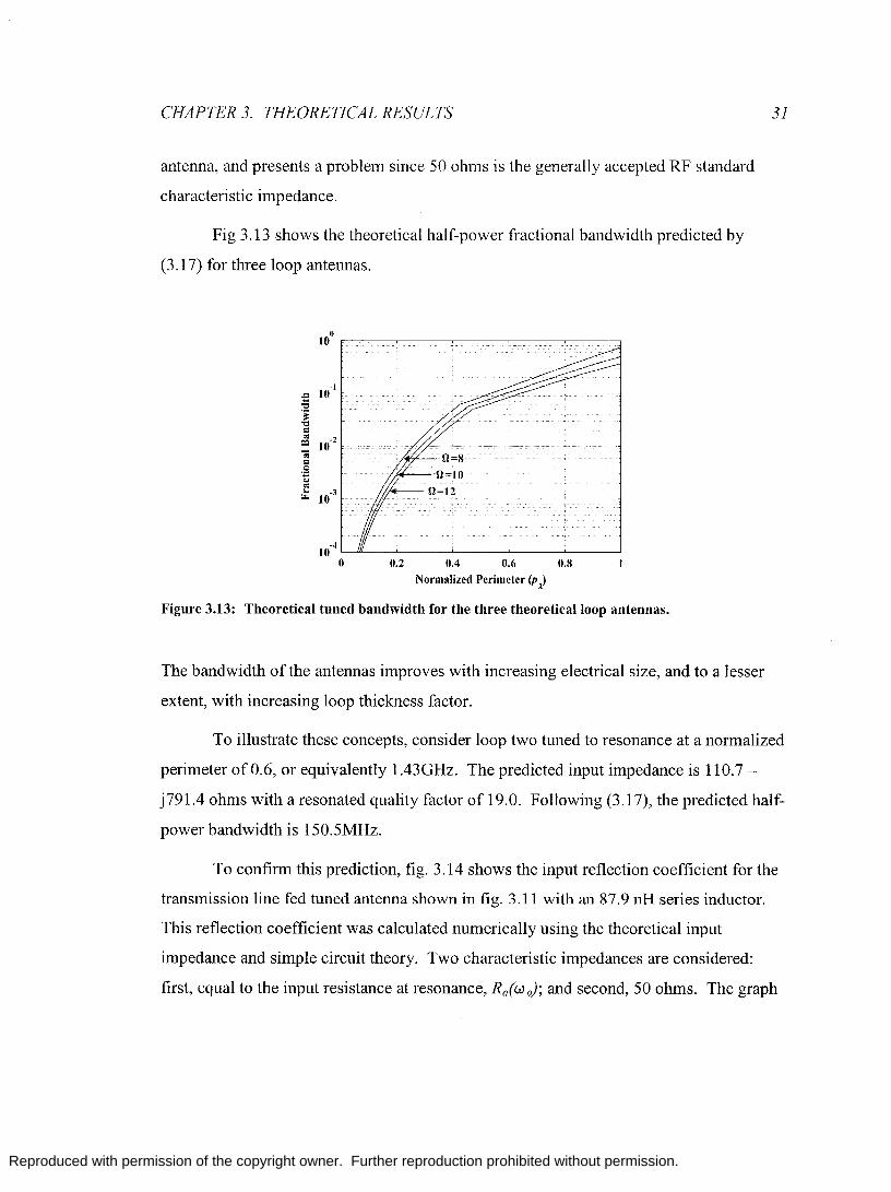
Figure 3.13: Theoretical tuned bandwidth for the three theoretical loop
antennas ...................................................................................................... 31
Figure 3.14: Input reflection coefficient and bandwidth of the example tuned
loop ............................................................................................................ 32
Figure 3.15: Two-element step-up matching network topology (Ra > Rin) .................... 33
Figure 3.16: Composite structure: transmission line feed, two-element matching
network, and tuned loop antenna ............................................................... 34
Figure 3.17: Quality factor of the tuned loop and nodal quality factor of the
matching network for the example loop antenna, loop two ....................... 35
Figure 3.18: Input reflection coefficient of the tuned antenna with and without
the additional matching network. ............................................................... 36
Figure 3.19: Composite structure with differential matching network and tuned
antenna ....................................................................................................... 36
Figure 4.1: Half-loop impedance measurement setup .................................................. 37
Figure 4.2: Measured and theoretical input resistance for loop one (0 = 8) ................ 39
Figure 4.3: Measured and theoretical input reactance for loop one (0 = 8) ............... .40
Figure 4.4: Measured and theoretical input resistance for loop two (0 = 10) ............ .40 IX
Reproduced with permission of the copyright owner. Further reproduction prohibited without permission.
Figure 4.5: Measured and theoretical input reactance for loop two (n = 10) ............. .41
Figure 4.6: Measured and theoretical input resistance for loop three (n = 12) .......... .41
Figure 4.7: Measured and theoretical input reactance for loop three (n = 12) ........... .42
Figure 4.8: Dimensions of the Wheeler cap used to measure the loop antenna
radiation efficiencies ................................................................................. .44
Figure 4.9: Measured input reactance of loop two in free-space and with the
Wheeler cap. The measured frequency range is from 0.3 MHz to
2 GHz ......................................................................................................... 45
Figure 4.1 0: Measured input reactance ofloop three in free-space and with the
Wheeler cap. The measured frequency is from 0.3 MHz to
725 MHz .................................................................................................... 45
Figure 4.11: Measured and theoretically predicted radiation efficiency for loop
two (n = 10). The measured frequency range is from 0.3 MHz to
Figure 4.12:
Figure 4.13:
Figure 5.1:
Figure 5.2:
Figure 5.3:
Figure 5.4:
Figure 5.5:
Figure 5.6:
2 GHz ......................................................................................................... 46
Measured and theoretically predicted radiation efficiency for loop
three (n = 12). The measured frequency is from 0.3 MHz to
725 MHz .................................................................................................... 47
Measured and theoretical radiation efficiency for loops 2 and 3.
The measured results are the fitted curves, not the raw data .................... .48
Final tag design with electronics and loop antenna .................................. .49
Prototype antenna overview ....................................................................... 50
Finished prototype antenna ........................................................................ 51
Cross-sectional area comparison between thin-wire and a PCB
trace ............................................................................................................ 53
PCB antenna dimensional restrictions ....................................................... 54
Simulated radiation efficiency versus trace width for the PCB loop
(from ADS Momentum) at a frequency of915MHz ................................. 56
x
Reproduced with permission of the copyright owner. Further reproduction prohibited without permission.
Figure 5.7: Gap-Fed loop antenna and equivalent circuit including feed-gap
capacitance ................................................................................................. 57
Figure 5.8: Numerically simulated surface current on both the loop antenna
and ground plane. A gap-voltage excitation is used ................................. 59
Figure 5.9: Surface current induced on ground plane .................................................. 59
Figure 5.10: Simulated input resistance and input reactance. The lower and
upper frequencies are 800 MHz and 1.0 GHz respectively ....................... 60
Figure 5.11: Radiation quality factor calculated using the CST generated input
impedance. The Chu (single mode) limit is included for reference .......... 61
Figure 5.12: CST simulated far-field pattern GoC8 = 90°, @) for prototype
antenna ....................................................................................................... 62
Figure 5.13: CST simulated far-field pattern for prototype antenna. The dashed
line is Go(8, @ = 90°) and the solid line is Ge(8, @ = 90°) .......................... 63
Figure 5.14: CST simulated far-field pattern cut GoC8, @ = 0°) for prototype
antenna ....................................................................................................... 63
Figure 5.15: Differential to single-ended matching network. ........................................ 64
Figure 5.16: Series tuned loop antenna (single-ended) .................................................. 65
Figure 5.17: Two-element step-down matching network topology (single-
ended) ......................................................................................................... 65
Figure 5.18: Single-ended discrete matching network ................................................... 66
Figure 5.19: Final matching network. ............................................................................ 67
Figure 5.20: VNA measurement of antenna input impedance ....................................... 68
Figure 5.21: Measured loop input impedance and simulated CST input
impedance .................................................................................................. 70
Figure 5.22: Measured nodal impedance with C] = 0.8pF, C3 = 0.7pF. The
nodal impedance at 915 MHz (circled) is 6 + j27 ohms ............................ 71
Xl

Reproduced with permission of the copyright owner. Further reproduction prohibited without permission.
Figure 5.23:
Figure 5.24:
Figure 5.25:
Figure 5.26:
Figure 5.27:
Figure 5.28:
Figure 6.1:
Figure A.l:
Figure A.2:
Measured nodal impedance with C1 = 0.8pF, C3 = 0.7pF, and
C2 = 5.0pF. The nodal impedance at 915 MHz (circled) is
166 + j5.3 ohms ......................................................................................... 71
Measured input impedance of the antenna with complete matching
network. The input impedance at 915 MHz (circled) is
43.2+ j8.8 ohms ......................................................................................... 73
Measured return loss of the antenna with matching network. The
return loss at 915 MHz (circled) is -18.5 dB ............................................. 73
Measured (dashed line) and simulated far-field pattern
IG(8 = 900, 0)1 for the prototype antenna ................................................... 74
Measured (dashed line) and simulated (solid line) far-field pattern
IG(8, 0 = 900 )1 for the prototype antenna ................................................... 75
Measured (dashed line) and simulated (solid line) far-field pattern
10(8,0 = 00 )1 for prototype antenna ........................................................... 75
Theoretically derived radiation efficiency and maximum tuned
bandwidth of a thin-wire loop antenna with radius of 20mm and
loop thickness factor, 0, of 10 ................................................................... 77
Prototype antenna matching network ......................................................... 78
Prototype antenna matching network. ........................................................ 79
XlI

Reproduced with permission of the copyright owner. Further reproduction prohibited without permission.
List of Tables
Table 2.1: Loop dimensions ofthe three theoretical loops .......................................... 5
Table 4.1: Loop dimensions of the three measured half-loops .................................. 38
Table 4.2: Measured and theoretically predicted locations ofthe first anti-
resonance in the loop input impedances .................................................. .42
Xlll

Reproduced with permission of the copyright owner. Further reproduction prohibited without permission.
Chapter 1
Introduction
Modern integrated circuit technology has advanced to the point where single chip
digital transceivers can transmit power levels in excess of 10dBm and have receive
sensitivities on the order of -115dBm 1. These transceivers, combined with low-power
microprocessors, form the building blocks of compact wireless tags capable of intra-tag
communication over hundreds of meters. Tag to base-station ranges can be even greater
with high-gain antenna arrays and more sophisticated digital signal processing available
at the base-station. Examples of these systems include wireless sensor networks,
implanted and external wireless medical devices, and wireless monitoring at home and in
industry.
The battery and antenna are typically the limiting factors in the physical size of
compact wireless tags. A compact antenna with high radiation efficiency maximizes the
system performance while reducing demands on the battery, allowing further reduction in
physical size.
The planar shape of the loop antenna makes it ideal for use as a compact antenna;
however, like most other compact antennas, the electrically small loop suffers from poor
radiation efficiency. Owing to this poor radiation efficiency, it has traditionally been
I Examples include Analog Device's AD7020 transceiver and Integration Associates' IA4420 transceiver. 1

Reproduced with permission of the copyright owner. Further reproduction prohibited without permission.
CHAPTER 1. INTRODUCTION 2
limited to applications that are low-range, low data-rate communications or receive only
systems such as pagers and AM radio.
The loop antenna is especially suitable for implanted wireless communications
because its magnetic dominated near fields do not experience the same degree of tissue
loading as do compact electric antennas.
This thesis examines the loop antenna as a compact antenna. It investigates how
the radiation efficiency of a loop antenna is drastically improved by increasing the
electrical size beyond the small loop threshold. The small loop threshold is normally
defined by setting the normalized perimeter,
P PA = A' (1.1)
where P is the perimeter of the loop and A is the electromagnetic wavelength, to be one
third. The focus of this work is the region between the electrically small loop and the
one-wavelength loop. The theoretical radiation efficiency at the upper end of this region
will be shown to approach unity. The author has not been able to find previous work that
specifically characterises this improvement in radiation efficiency.
Much information on the small loop antenna is readily available; however, it is of
little use if an efficient antenna is needed, and most existing work on the electrically large
loop antenna is overly academic and mathematically complex. A significant contribution
of this work is extracting and assembling information beneficial to the practicing
engineer from close to a century of academic study on the electrically large loop. Input
impedance, appropriate impedance matching networks, and resulting tuned bandwidth are
all considered.
Several thin-wire loops were built to confirm the predicted theoretical behaviour.
Although rare, other authors have published measurements of the input impedance of
electrically large loops. The radiation efficiency of these loops was also measured using

Reproduced with permission of the copyright owner. Further reproduction prohibited without permission.
CHAPTER 1. INTRODUCTION
the Wheeler cap technique. Similar measurements of radiation efficiency are not
available in the literature.
3
Finally, the development and testing of a compact loop antenna for use in a
compact RF tag is covered, and the design of this antenna utilises many of the concepts
from the other chapters. Measurements of input impedance, tuned bandwidth, radiation
patterns, and radiation efficiency are presented and compared with predicted values from
numerical simulations.
Reproduced with permission of the copyright owner. Further reproduction prohibited without permission.
Chapter 2
Existing Theoretical Analysis
The first documented theoretical analysis of the electrically large thin-wire loop antenna
is Pocklington's work (1897) who studied the receiving properties of such a loop [1].
Over a century has passed since this initial consideration of the electrically large loop,
and in that time a huge amount of work has been contributed by many different authors;
however, only a handful of these papers contribute a truly fundamental new development.
The purpose of this chapter is to review key developments, and extract information
relative to our interest in the compact loop antenna from previous work.
2.1 Loop Antenna Dimensions
Most of the academic work on the electrically large loop antenna is restricted to
the thin-wire loop: a loop made from wire with a circular cross-section. The loop
thickness factor,
(2.1)
is commonly used in the literature to quantify the relative thickness of the loop conductor
to the radius of the loop, where the dimensions a and b are shown in fig. 2.1. The
thickness factor and normalized perimeter completely describe the electromagnetic
4

Reproduced with permission of the copyright owner. Further reproduction prohibited without permission.
CHAPTER 2. EXISTING THEORETICAL ANALYSIS
radiation characteristics of the loop. Absolute dimensions are required only if ohmic
losses need to be considered.
Figure 2.1: Thin-wire loop dimensions.
The three theoretical loops, given in table 2.1, are considered throughout the
second and third chapters of this thesis. All three loops have the same perimeter, but a
different thickness factor. Loop one, with a thickness factor of 8, is considered a thick
wire loop, whereas loop three, with a thickness factor of 12, is considered a thin-wire
loop. These choices allow changes in loop thickness factor to be quantitatively analyzed
independent from other parameters
Table 2.1: Loop dimensions of the three theoretical loops.
a (mm) b(mm) p(mm) n Loop 1 2.3 20 125.7 8
Loop 2 0.85 20 125.7 10
Loop 3 0.31 20 125.7 12
2.2 Small Loop Theory
5
Small loop theory is well established and is covered in most of the classic
introductory antenna textbooks [2], [3], and [4]. It assumes a uniform current distribution

Reproduced with permission of the copyright owner. Further reproduction prohibited without permission.
CHAPTER 2. EXISTING THEORETICAL ANALYSIS 6
along the length of the antenna, but as the frequency increases, the wavelength becomes
comparable to the length of the antenna, and this assumption is no longer valid. Beyond
this threshold the small loop equations no longer accurately describe the electromagnetic
behaviour of the loop. The small loop threshold is generally accepted to be a normalized
loop perimeter, PI.., somewhere between one tenth and one third2•
Small loop radiation resistance,
(2.2)
is dependent on only the wavenumber, k, and cross-sectional area, A, of the loop [3]. A
more convenient form for a circular loop is obtained by expressing the area in terms of
the normalized loop perimeter
(2.3)
The expression for ohmic loss,
(2.4)
is derived from skin depth equations [5]. Unlike radiation resistance, ohmic loss depends
on the wavelength and the physical size of the loop, as shown by re-arranging (2.4)
Radiation efficiency,
R 17= rad,
Rrad +Rn
is expressed in terms of both ohmic loss and radiation loss.
2 There is some disagreement amongst the classic antenna texts about the small loop threshold; Krauss gives 0.33, Stutzman gives 0.3, and Balanis gives 0.1 [2], [3], [4].
(2.5)
(2.6)
Reproduced with permission of the copyright owner. Further reproduction prohibited without permission.
CHAPTER 2. EXISTING THEORETICAL ANALYSIS 7
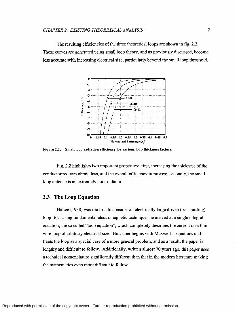
The resulting efficiencies of the three theoretical loops are shown in fig. 2.2.
These curves are generated using small loop theory, and as previously discussed, become
less accurate with increasing electrical size, particularly beyond the small loop threshold.
0r-~~~~~~~~~~~
-1
-2
-3
== ~ -4 ,.:; .-~ -5 .y IS -6 I;;;J
-7
-8
-9
-10 '-----'-'L...LJ..../..-----'--_'---'-_'-----'-_'---'----'
o 0.05 0.1 0.15 0.2 0.25 0.3 0.35 0.4 0.45 0.5 Normalized Perimeter (p j)
Figure 2.2: Small loop radiation efficiency for various loop thickness factors.
Fig. 2.2 highlights two important properties: first, increasing the thickness of the
conductor reduces ohmic loss, and the overall efficiency improves; secondly, the small
loop antenna is an extremely poor radiator.
2.3 The Loop Equation
Hallen (1938) was the first to consider an electrically large driven (transmitting)
loop [6]. Using fundamental electromagnetic techniques he arrived at a single integral
equation, the so called "loop equation", which completely describes the current on a thin
wire loop of arbitrary electrical size. His paper begins with Maxwell's equations and
treats the loop as a special case of a more general problem, and as a result, the paper is
lengthy and difficult to follow. Additionally, written almost 70 years ago, this paper uses
a technical nomenclature significantly different than that in the modem literature making
the mathematics even more difficult to follow.
Reproduced with permission of the copyright owner. Further reproduction prohibited without permission.
CHAPTER 2. EXISTING THEORETICAL ANALYSIS
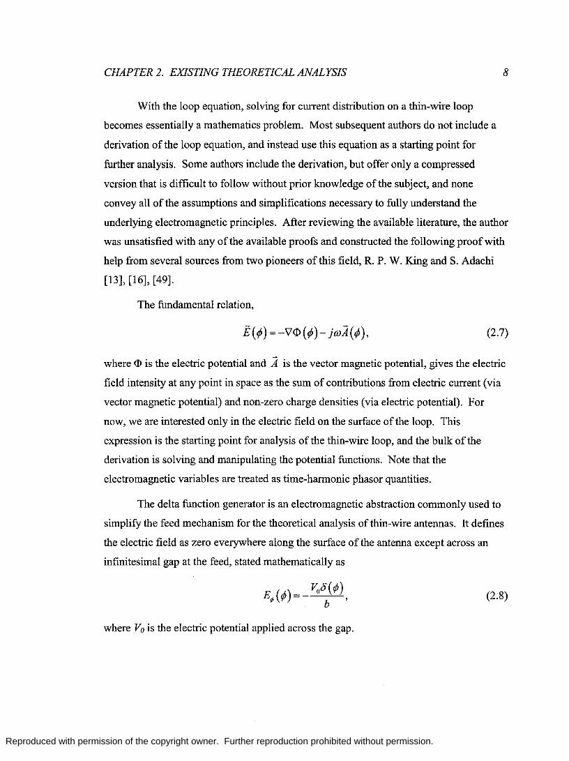
With the loop equation, solving for current distribution on a thin-wire loop
becomes essentially a mathematics problem. Most subsequent authors do not include a
derivation of the loop equation, and instead use this equation as a starting point for
further analysis. Some authors include the derivation, but offer only a compressed
version that is difficult to follow without prior knowledge of the subject, and none
8
convey all of the assumptions and simplifications necessary to fully understand the
underlying electromagnetic principles. After reviewing the available literature, the author
was unsatisfied with any of the available proofs and constructed the following proof with
help from several sources from two pioneers of this field, R. P. W. King and S. Adachi
[13], [16], [49].
The fundamental relation,
E(~) = -V<l>(~)- jaJA(~), (2.7)
where <1> is the electric potential and A is the vector magnetic potential, gives the electric
field intensity at any point in space as the sum of contributions from electric current (via
vector magnetic potential) and non-zero charge densities (via electric potential). For
now, we are interested only in the electric field on the surface of the loop. This
expression is the starting point for analysis of the thin-wire loop, and the bulk of the
derivation is solving and manipulating the potential functions. Note that the
electromagnetic variables are treated as time-harmonic phasor quantities.
The delta function generator is an electromagnetic abstraction commonly used to
simplify the feed mechanism for the theoretical analysis of thin-wire antennas. It defines
the electric field as zero everywhere along the surface of the antenna except across an
infinitesimal gap at the feed, stated mathematically as
(2.8)
where Vo is the electric potential applied across the gap.
Reproduced with permission of the copyright owner. Further reproduction prohibited without permission.
CHAPTER 2. EXISTING THEORETICAL ANALYSIS 9
Several key assumptions must be stated before continuing. An ideal conductor is
assumed, so all currents and free-charges are constrained to the surface of the loop. A
thin-wire loop is assumed, where the thin-wire loop criteria is stated mathematically as
a2 « b2 and (kai« 1. As a result, the surface current and free charge densities are both
assumed to have uniform radial distribution around the cross-section of the conductor.
Finally, the current is assumed to have only components in the phi, fiJ, direction.
The free-charge density, p (¢/), can now be replaced with an equivalent charge
per unit length, q (¢/) = (21ra ) p (¢') , and the surface current density, J (¢') , is replaced
with total current, j (¢') = (21ra )J(¢').
The electric (scalar) potential,
<J>(¢) = -l-f q(¢') e-ikR
dS' 41r& s· 21ra R '
(2.9)
is based on a differential surface instead of a differential volume, and requires evaluation
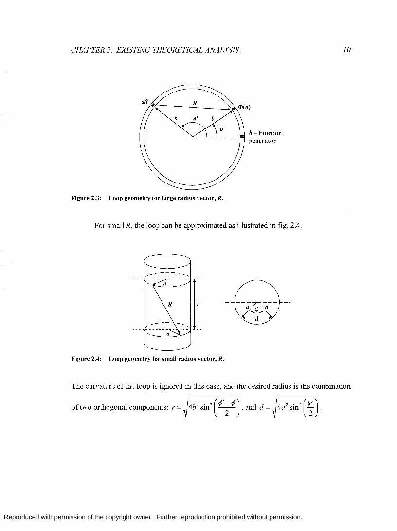
of the radius, R, shown in fig. 2.3, from the elemental surface at fiJ' to the observation
point on the surface of the loop at fiJ. If the radius is much larger than the thickness of the
loop, the latter can be neglected and the approximation
(2.10)
is used.
Reproduced with permission of the copyright owner. Further reproduction prohibited without permission.
CHAPTER 2. EXISTING THEORETICAL ANALYSIS
Figure 2.3: Loop geometry for large radius vector, R.
0- function generator
For small R, the loop can be approximated as illustrated in fig. 2.4.
R r
Figure 2.4: Loop geometry for small radius vector, R.
10
The curvature of the loop is ignored in this case, and the desired radius is the combination
of two orthogonal components: r = 4b2 sin2 (1/ ~rjJ), and d = 4a 2 sin2 (~) •

Reproduced with permission of the copyright owner. Further reproduction prohibited without permission.
CHAPTER 2. EXISTING THEORETICAL ANALYSIS 11
The resulting general expression
(2.11)
is valid for both cases (small and large R), and the expression for electric potential is
now
<D(¢)=_l_¢'j VIS q(¢')e-ikR
(a.dlf/)(b.d¢'). 47r£ ¢'=-Jr VI=-Jr 27ra R
(2.12)
Note, the differential surface in (2.12) has been expanded as a product of two differential
lengths.
The kernel function
Jr b - jkR
W(¢-¢')= f-_e ·-dlf/ 27r R
-Jr
is commonly used in the literature, and simplifies the scalar potential as
¢'=rr
<D(¢) =_1 f q(¢')W(¢-¢')d¢'. 47r£ ¢'=-rr
(2.13)
(2.14)
The vector magnetic potential uses the same Green's function as the electric
potential, but the magnetic potential is more complicated because of its vector nature.
The current vector at the differential surface, dS', is expressed in terms ofthe
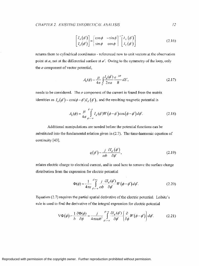
cylindrical unit vectors I R, (¢') and I¢, (¢'). The matrix identity
[Ix (¢')] = [cos¢' -sin¢'][IR, (¢')] Iy (¢,) sin¢' cos¢' I¢, (¢')
(2.15)
converts this current vector from cylindrical to cartesian coordinates, and the inverse
matrix operation
Reproduced with permission of the copyright owner. Further reproduction prohibited without permission.
CHAPTER 2. EXISTING THEORETICAL ANALYSIS 12
(2.16)
returns them to cylindrical coordinates - referenced now to unit vectors at the observation
point at 13, not at the differential surface at 13'. Owing to the symmetry of the loop, only
the 13 component of vector potential,
needs to be considered. The 13 component of the current is found from the matrix
identities as I¢ (rjJ') = cos(rjJ - rjJ')I¢. (rjJ'), and the resulting magnetic potential is
(2.17)
(2.18)
Additional manipulations are needed before the potential functions can be
substituted into the fundamental relation given in (2.7). The time-harmonic equation of
continuity [43],
q (rjJ') = L 8I¢, (rjJ') OJb 8rjJ' ,
(2.19)
relates electric charge to electrical current, and is used here to remove the surface charge
distribution from the expression for electric potential
(2.20)
Equation (2.7) requires the partial spatial derivative of the electric potential. Leibitz's
rule is used to find the derivative of the integral expression for electric potential
(2.21 )

Reproduced with permission of the copyright owner. Further reproduction prohibited without permission.
CHAPTER 2. EXISTING THEORETICAL ANALYSIS
The identity 8W = - 8W , provided by King, is used to re-arrange this differential 8¢ 8¢'
expreSSIon,
V<I>(¢)=- 4":Wb,:I aJ~;~') t3~,W(¢-f)}d¢' ~
g(¢')
Given the condition I¢, (¢') g (¢')I;:::Jr = 0, integration by parts reduces to
I aI~~~') g(¢')d¢' = -I I, (¢') ~~') d¢',
13
(2.22)
(2.23)
and is used to rearrange (2.22) into a form more easily combined with the expression for
magnetic potential (2.18)
1 8<l>(¢) = j 2 ¢T I¢,(¢') { ~2, W(¢-¢')}d¢', b 8¢ 41fcOJb ¢,=-Jr 8 ¢
(2.24)
Finally, the free-space electromagnetic relations Co = J.1~ and OJ = 17ok
o are used 170 J.10
to arrive at the familiar form of the loop equation
This integral equation completely describes the current distribution on the voltage driven
thin-wire loop, and the only unknown is the current itself.

Reproduced with permission of the copyright owner. Further reproduction prohibited without permission.
CHAPTER 2. EXISTING THEORETICAL ANALYSIS 14
2.4 Solving the Loop Equation
The loop equation was first derived by Hallen. He was also the first to attempt to
solve this equation using a Fourier series expansion to describe the current distribution
(2.26)
The mathematical process of determining the current distribution, and in tum the Fourier
coefficients, an, that satisfy the loop equation (2.25) is extremely difficult, and Hallen
was unable to find an expression for the coefficients that resulted in a convergent series.
Note that the Fourier coefficients, an, should not be confused with the wire radius, a.
Nearly twenty years later (1956), Storer was the first to successfully find a
solution for the Fourier coefficients and numerically calculate the resulting current
distributions and input impedance for various loops [7]. Once the current distribution is
found, the input admittance, and input impedance, easily follows as
(2.27)
His approach truncated the series at five terms and replaced the rest of the terms with an
equivalent integral.
In the same year, Kennedy published the first documented electrically large loop
antenna input impedance measurements [8]. Using a half-loop over an image plane she
measured the current distribution by physical probing and estimated the resulting
admittance of a loop with thickness factor n = 11. Despite admitted shortcomings in her
impedance measurements, the measured conductance is in quite good agreement with
Storer's theoretical value; however, there is a greater discrepancy between the measured
and theoretical susceptances.

Reproduced with permission of the copyright owner. Further reproduction prohibited without permission.
CHAPTER 2. EXISTING THEORETICAL ANALYSIS 15
In 1962 T.T. Wu published what is now the accepted technique for detennining
the Fourier coefficients [9]. His briefpaper questions the validity of Storer's approach,
and presents an alternative mathematical procedure to obtain the Fourier coefficients, but
does not calculate the resulting impedances. By considering the thickness of the
conductor in more detail, Wu's derivation of the Green's function is more general than
those previously considered.
King et. al released series of papers in 1963, 1964 and 1965 investigating the
properties of a driven circular thin-wire loop immersed in a dissipative medium [10],
[11], [12]. The second paper is the first to calculate current distributions and resulting
impedances using Wu's approach. King calculated the admittance as a function of the
number of Fourier tenns to a maximum of twenty tenns. His results showed that the
conductance quickly converges with 8 tenns included in the series; however, the
susceptance continues to increase with the number oftenns. The rate of increase is more
pronounced for thicker loops (0 < 10) and for larger electrical sizes. He noted the
conductance is very similar to Storer's results, which had already been shown to agree
well with Kennedy's experimental data. The susceptance has more significant
differences when compared with Storer's results, but the comparison isn't as meaningful
since Storer's susceptance did not agree well with measurements.
King also made some key observations about the voltage delta-function generator
which is purely a mathematical abstraction, and is unrealizable in practice. While it
results in an accurate prediction of the current distribution and conductance, the
infinitesimally small feed gap results in an infinite susceptance. As a result of the
limitations of the delta-function generator, King makes the following conclusions on
Wu's technique: "These results indicate that a Fourier Series solution in which 20 tenns
are retained is satisfactory for detennining the admittance ofthin-wire loops (0 2::10) that
are not too large ({3d ::;2.5)"; and "The approximation is excellent for the conductance,
somewhat less accurate for the susceptance".
Reproduced with permission of the copyright owner. Further reproduction prohibited without permission.
CHAPTER 2. EXISTING THEORETICAL ANALYSIS 16
G. S. Smith continued to work on loop antennas in homogeneous matter
throughout the 1970s, and included some research on measuring the radiation resistance
of loops with a wheeler cap [14], [15], [42]. Smith and King's work on loops in lossy
matter are excellent references for embedded loop antennas [16]. This topic has recently
showed renewed academic interest with the advent of surgically implanted wireless
medical devices.
Interestingly, most of this research on loop antennas stems from Harvard
University where Storer, King, Wu and Smith were all either faculty or graduate students.
In more recent literature, Zhou and Smith (1991) circumvent the susceptance
problems associated with a delta-function generator by considering a coaxial fed loop
antenna over an infinite image plane [18]. They model the coaxial feed as a magnetic
frill which impresses a driving current onto a full loop and add a correction term to Wu's
solution. Their measured impedances are in remarkable agreement with their
theoretically predicted impedances.
Finally, the work of S. Adachi and Y. Mushiake should be included in this brief
review. They published three papers in 1957 that formed a complete and concise analysis
of the electrically large loop antenna. The first paper derives an alternate form of the
loop equation [49], and following some simplifications, derives a closed form solution for
the current distribution. The second paper calculates various electrical properties of the
loop based on the current distribution obtained from the original paper [50], and the third
paper considers a loop antenna parallel to a ground plane forming a more directional
antenna [51]. Strangely, references to this work in the modem literature are scarce even
though Adachi continued to publish research on the loop well into the 1970s.

Reproduced with permission of the copyright owner. Further reproduction prohibited without permission.
CHAPTER 2. EXISTING THEORETICAL ANALYSIS 17
2.5 Radiation Fields
This thesis does not examine theoretical expressions for the radiation fields of a
loop antenna; however, much work has been done on the subject and a brief review of the
available literature is included here.
The first authors to consider the radiation field of the electrically large thin-wire
loop were Sherman (1944) and Glinski (1947) [19], [20]. Both authors used assumptions
for the current distribution on the loop because these papers were published before the
current distribution problem had been solved. Sherman assumed a sinusoidal current
distribution, and Glinski used a transmission line as a model for the current distribution
on a loop. Following these original papers, Martin (1960) expanded on the sinusoidal
distribution, and Lindsay (1960) expanded on the transmission line model distribution
[21], [22].
Rao (1968) was the first to numerically calculate the far-field patterns of the loop
antenna using the Fourier series current distribution [23].
Much of the recent research on loop antennas deals with analytical calculations of
the radiation field using the Fourier series current distribution [24], [25], [28], and in
particular, exact expressions for the more complicated near-fields. This subject is of
interest because ofSAR (specific absorption rate) concerns with implanted antennas and
antennas used in close proximity to the human body.

Reproduced with permission of the copyright owner. Further reproduction prohibited without permission.
Chapter 3
Theoretical Results
The current distribution on a thin-wire antenna detennines practically all other
properties of interest such as input impedance, radiation efficiency, far-field patterns, and
quality factor and tuned bandwidth. The King / Wu solution for the Fourier coefficients,
an, is used throughout this chapter to describe the current distribution,
- jV ( 1 ~ cos(n¢)) I¢(¢) = __ 0 -+2~ , ~07[ ao I an
(3.1)
for the three loops presented in section 2.1. The expressions for the Fourier coefficients
are tedious, and must be evaluated numerically. Readers are referred to several
references for a succinct overview of the Fourier coefficient evaluation [9], [18].
3.1 Current Distribution
Fig. 3.1 shows both the Fourier series current distribution and the sinusoidal
current distribution given by
18
(3.2)

Reproduced with permission of the copyright owner. Further reproduction prohibited without permission.
CHAPTER 3. THEORETICAL RESULTS 19
Both solutions result in a standing current wave around the loop with a maximum
located 180 degrees from the feed location regardless of the electrical size of the loop.
This maxima must be located at the mid-point of the loop to maintain a symmetric
current distribution with respect to the feed location. Using the equation of continuity
(2.19), this standing wave current distribution can be shown to produce a similar surface
charge distribution.
8
7
6
5 ;::.~ -~
4
5: 3
PA = 3/2
PA = 112
2 3 4 5 6
¢, radians
Figure 3.1: Thin-wire loop current distribution from the Fourier series approximation and from the sinusoidal approximation for loop two (U = 10).
The sinusoidal approximation and the Fourier series solution tend to differ at the
driving point of the antenna. The input impedance is dependent on the current
distribution at the feed of the antenna, so the sinusoidal approximation is not well suited
to determining input impedances.
Fig. 3.2 shows the Fourier coefficients for the quarter wavelength loop,
p" = 114, and the one wavelength loop,p" = 1. The fundamental component, aj, is
dominant for one wavelength loop, but for smaller loops the electrical size is less than the
wavelength of this harmonic, and the uniform current component, ao, is dominant.

Reproduced with permission of the copyright owner. Further reproduction prohibited without permission.
CHAPTER 3. THEORETICAL RESULTS
10 Index (n)
15 20
Figure 3.2: First twenty Fourier coefficients, an, for loop two at two different electrical sizes.
20
The thin-wire loop criteria was stated as a2 «b2 and (ka)2 « 1, and accordingly
the current is assumed to be uniformly distributed around the perimeter of the conductor
as shown in fig. 3.3.
z+ I
Figure 3.3: Uniform cross-sectional current distribution.
-~ r
Balzano and Siwiak (1987) added a second dimension of basis functions,
orthogonal to the plane of the loop, to the existing Fourier basis functions [17]. Using
just two harmonics in this new direction, the distribution of the current around the cross
section of the conductor is investigated, and the thin-wire loop assumption is no longer
required.
The current density is now a function of two angular dimensions (@, 1/;)
Reproduced with permission of the copyright owner. Further reproduction prohibited without permission.
CHAPTER 3. THEORETICAL RESULTS 21
00 C()
Jq,(rp,z) = I I An,qe-inq,Fq(z). (3.3) n=-C/J q=-CI)
The two remaining assumptions are: first, the wire diameter is much smaller than
one wavelength; and second, current is restricted to the phi direction.
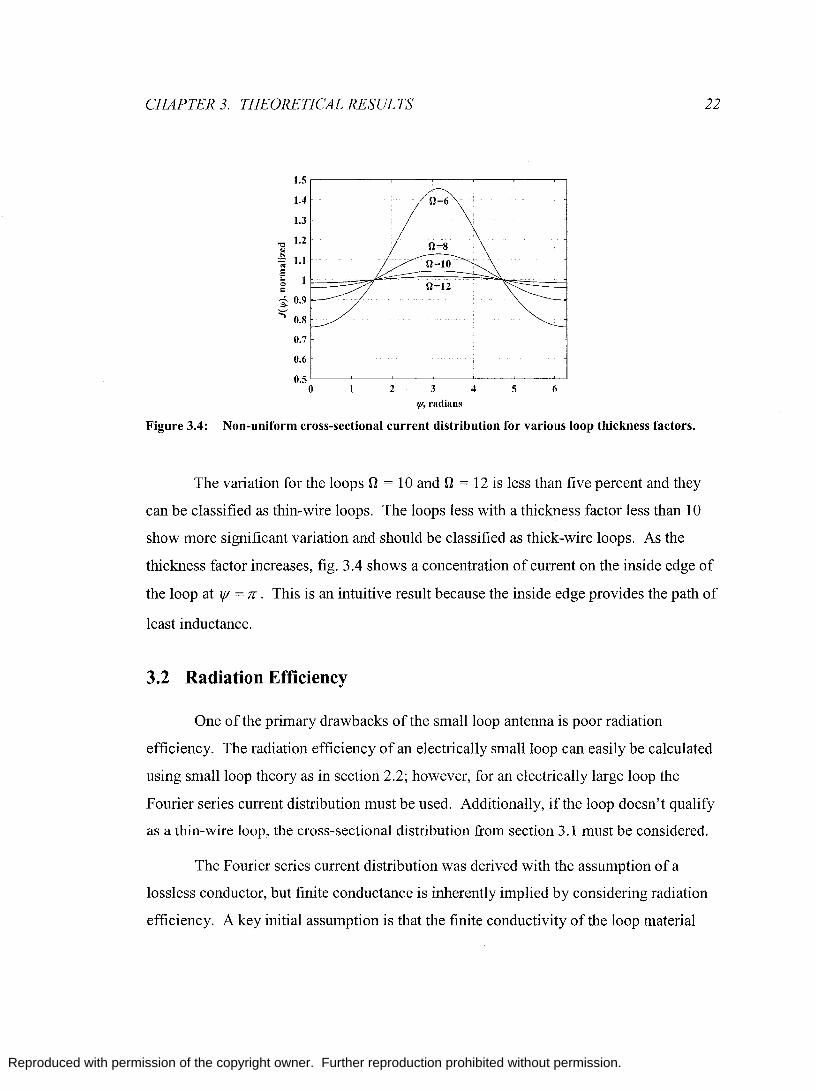
Balzano constructed two loops, a thin-wire loop with thickness factor 0 = 11, and
a thick-wire loop with 0 = 9. He measured the magnetic and electric field magnitudes in
the vicinity of the loops and found that the measurements agreed reasonably well his
theoretically calculated field strengths. Perhaps more interestingly, he observed from
both theoretical analysis and measurements that the current density around the cross
section of the conductor varies approximately as Jrp(¢,If/):::::; Jq,(rp,b,±a)J'I' (If/), where the
radial distribution around the cross-section of the wire,
is independent of the angle g. Fig. 3.4 shows the cross-sectional current density
distribution resulting from (3.4).
This relationship combined with the results of previous analysis gives
(3.4)
(3.5)
Reproduced with permission of the copyright owner. Further reproduction prohibited without permission.
CHAPTER 3. THEORETICAL RESULTS 22
1.5
1.4 0=6
1.3
'0 1.2 0=8
" .~ 1.1 .. 0=10 8 ... 0 0=12 = ~ 0.9 "=;'
0.8
0.7
0.6
0.5 0 2 3 4 5 6
If/, radians
Figure 3.4: Non-uniform cross-sectional current distribution for various loop thickness factors.
The variation for the loops n = 10 and n = 12 is less than five percent and they
can be classified as thin-wire loops. The loops less with a thickness factor less than 10
show more significant variation and should be classified as thick-wire loops. As the
thickness factor increases, fig. 3.4 shows a concentration of current on the inside edge of
the loop at If/' = 1C. This is an intuitive result because the inside edge provides the path of
least inductance.
3.2 Radiation Efficiency
One of the primary drawbacks of the small loop antenna is poor radiation
efficiency. The radiation efficiency of an electrically small loop can easily be calculated
using small loop theory as in section 2.2; however, for an electrically large loop the
Fourier series current distribution must be used. Additionally, if the loop doesn't qualify
as a thin-wire loop, the cross-sectional distribution from section 3.1 must be considered.
The Fourier series current distribution was derived with the assumption of a
lossless conductor, but finite conductance is inherently implied by considering radiation
efficiency. A key initial assumption is that the finite conductivity of the loop material

Reproduced with permission of the copyright owner. Further reproduction prohibited without permission.
CHAPTER 3. THEORETICAL RESULTS
does not significantly alter this distribution. This assumption should be valid for the
highly conductive metals used in the construction of antennas.
23
The current is no longer restricted to the surface of the conductor, but is treated as
having a uniform radial distribution from the surface of the conductor to a skin depth of
as is illustrated in fig. 3.5.
z ... I
-~ r
Figure 3.5: Cross-sectional current distribution and skin depth for finite conductance loop conductor.
(3.6)
The previously derived expressions for current density must be changed from a
surface current (Aim) to an equivalent current density (Alm2), and the resulting
current density is
(3.7)
The ohmic power loss is found by integrating the current density over the volume
of the loop
(3.8)
Reproduced with permission of the copyright owner. Further reproduction prohibited without permission.
CHAPTER 3. THEORETICAL RESULTS 24
The differential volume in (3.8) can be expressed as dV = 5 ( a . dlf ) (b· d ¢) ,
which allows the volume integral to be broken up into two independent one-dimensional
integrals
(3.9)
The first integral in (3.9) can be evaluated analytically, and the resulting expression for
ohmic loss is
(3.1 0)
The radiated power is found from the input impedance of the lossless loop,
(3.11)
and the radiation efficiency is
(3.12)
Fig. 3.6 shows the radiation efficiency for the three theoretical loops calculated
using (3.10) to (3.12) and the Fourier series current distribution. Small loop radiation
efficiency is also shown for reference. Surprisingly, small loop theory provides a very
good lower bound on radiation efficiency, even for the electrically large loop.

Reproduced with permission of the copyright owner. Further reproduction prohibited without permission.
CHAPTER 3. THEORETICAL RESULTS
O~~~~--~~~~~~~~
-1
-2
-3
-7
-8
-9
+-T'r'----- 0 =1 0
+--- 0=12
---- Fourier Expansion
.. _ .. _ ..... _ ........ - Small Loop
-10 '----'--'L-L.LL-~_~~_~~_~___' _ _'
o 0.05 0.1 0.15 0.2 0.25 0.3 0.35 0.4 0.45 0.5
Normalized Perimeter (p)
25
Figure 3.6: Theoretically derived radiation efficiency of the three theoretical loops. The radiation efficiency calculated using small loop theory is included for reference.
Clearly, the radiation efficiency of a smaUloop can be drastically improved by
increasing the electrical size. Each of the loops considered here has an efficiency loss of
less than -0.5 dB when the loop is half a wavelength in perimeter.
Radiation efficient at lower frequencies can be improved by using thicker loops.
For example, a loop with thickness factor n = 8 still shows good efficiency for a
normalized perimeter, p"" of 0.2.
The PIF A (planar inverted F antenna) is the currently favoured low-profile
compact element. The air substrate PIF A must have dimensions of roughly one-quarter
wavelength by one-half wavelength, and requires a ground plane with dimensions of
roughly one wavelength. As an alternative, consider a circular loop with perimeter of
half-wavelength. The diameter of this circular antenna is~, demonstrating that the 2n
loop is hard to beat for an efficient and compact planar antenna.
Reproduced with permission of the copyright owner. Further reproduction prohibited without permission.
CHAPTER 3. THEORETICAL RESULTS 26
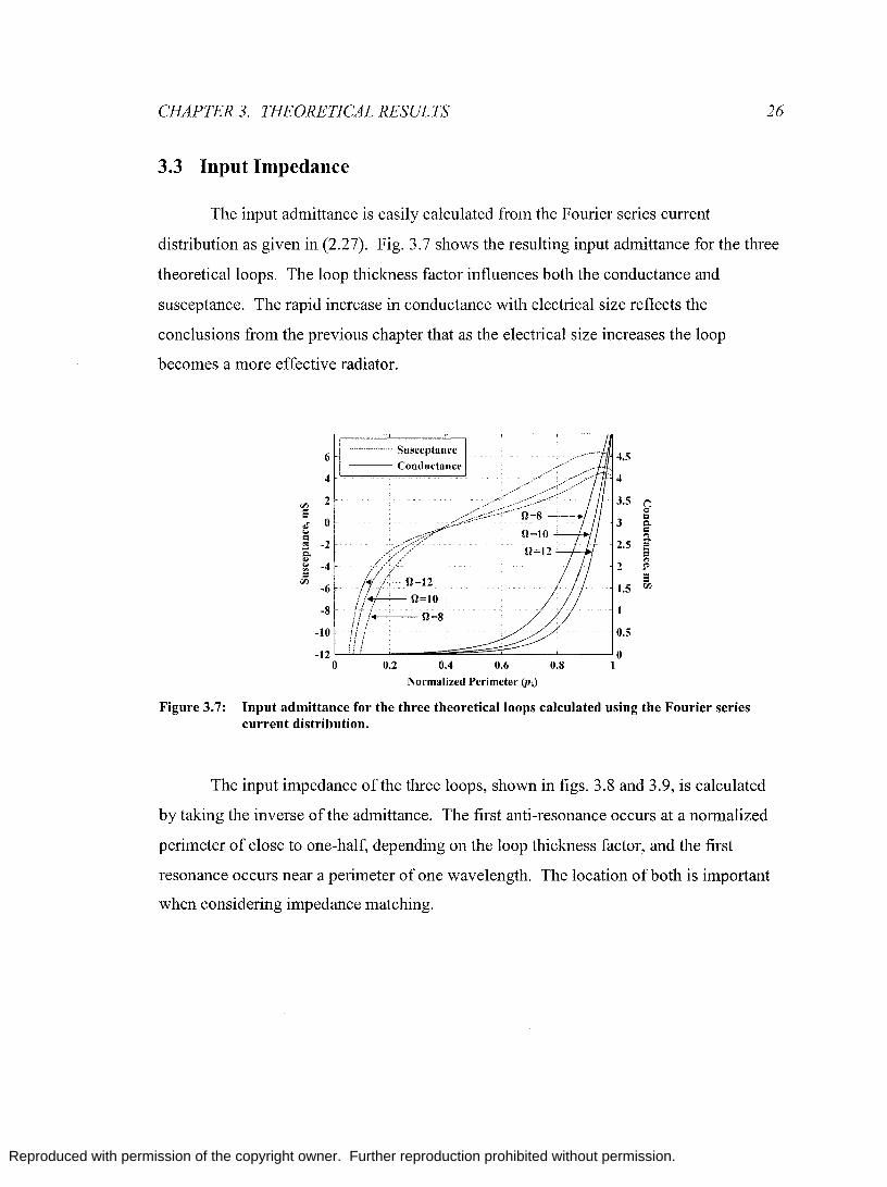
3.3 Input Impedance
The input admittance is easily calculated from the Fourier series current
distribution as given in (2.27). Fig. 3.7 shows the resulting input admittance for the three
theoretical loops. The loop thickness factor influences both the conductance and
susceptance. The rapid increase in conductance with electrical size reflects the
conclusions from the previous chapter that as the electrical size increases the loop
becomes a more effective radiator.
.................. Susceptance 6
4~~------------~
----- Conductance
f/J 2 S oS 0 .... = -is -2 & ~ -4 =
1JJ -6 /1.1-- 0=10 -s /i j II ;- O=S
-10 if I
---
/ __ ....... -........ , 4.5
3.5 ('"l
3 Q
= == ::;. 2.5 S .., 2 ."
i3 1.5 rJ1
0.5
-12 LJILI L! _-'--_ ..... ..,;;;;;;;;;;;;;;;;~£::::::::..._---L... __ -.J 0 o 0.2 0.4 0.6 O.S 1
Normalized Perimeter (PJ
Figure 3.7: Input admittance for the three theoretical loops calculated using the Fourier series current distribution.
The input impedance of the three loops, shown in figs. 3.8 and 3.9, is calculated
by taking the inverse of the admittance. The first anti-resonance occurs at a normalized
perimeter of close to one-half, depending on the loop thickness factor, and the first
resonance occurs near a perimeter of one wavelength. The location of both is important
when considering impedance matching.

Reproduced with permission of the copyright owner. Further reproduction prohibited without permission.
CHAPTER 3. THEORETICAL RESULTS
II/
104 n=10 -- +-- n=12
'" = .c 0 .. 3 .. 10 = ~ .;;
" ;:::
102
10· 0 0.2 0.4 0.6 0.8
No.·malized Peri mete.' (p..>
Figure 3.8: Input resistance for the three theoretical loops calculated using the Fourier series current distribution.
'" 8 .c 0 .. '"' = .s <I
'" " ;:::
4 X 10
1.5 ,..-----,----.,----,------,------,
n=12--
0.5 n=10_j
n=8.::J
0
-0.5
-J
-1.5 0 0.2 0.4 0.6 0.8
Normalized Perimeter (p..>
Figure 3.9: Input reactance for the three theoretical loops calculated using the Fourier series current distribution.
27
As previously mentioned in section 2.2, there is some disagreement about the
location of the small loop threshold. One measure of this location is the difference
between the small loop input resistance and the input resistance obtained from the Fourier
series current expansion, shown in Fig. 3.10 for loop two.
Reproduced with permission of the copyright owner. Further reproduction prohibited without permission.
CHAPTER 3. THEORETICAL RESULTS 28
25 //
0.25 /
Resistance / /
-------------------- % Difference //
20 /
/ 0.2 .. <.I C ~ .. ... '" ~ 15 0.15 '" ""' .- i ~ ~/~
~
= .. " ell J!' " .- Q .... /' = 10 .- 0.1 =-..
////"//'
3 <.I ... Fourier Series '" .. =- Expansion --.
5 i 0.05
o 0 0.05 0.06 0.07 0.08 0.09 0.1 0.11 0.12 0.13 0.14
Normalized Perimeter (PA)
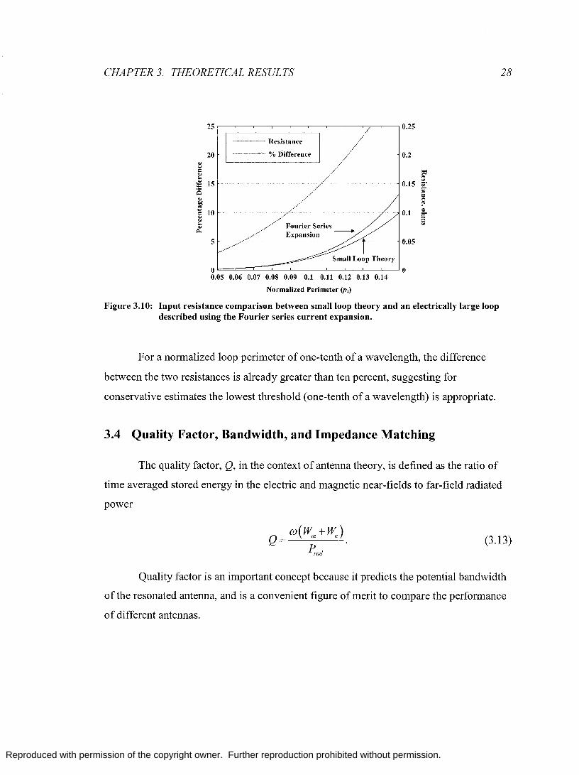
Figure 3.10: Input resistance comparison between small loop theory and an electrically large loop described using the Fourier series current expansion.
For a normalized loop perimeter of one-tenth of a wavelength, the difference
between the two resistances is already greater than ten percent, suggesting for
conservative estimates the lowest threshold (one-tenth of a wavelength) is appropriate.
3.4 Quality Factor, Bandwidth, and Impedance Matching
The quality factor, Q, in the context of antenna theory, is defined as the ratio of
time averaged stored energy in the electric and magnetic near-fields to far-field radiated
power
Q = w(Wm + W,,). P,·ad
(3.13)
Quality factor is an important concept because it predicts the potential bandwidth
of the resonated antenna, and is a convenient figure of merit to compare the performance
of different antennas.
Reproduced with permission of the copyright owner. Further reproduction prohibited without permission.
CHAPTER 3. THEORETICAL RESULTS 29
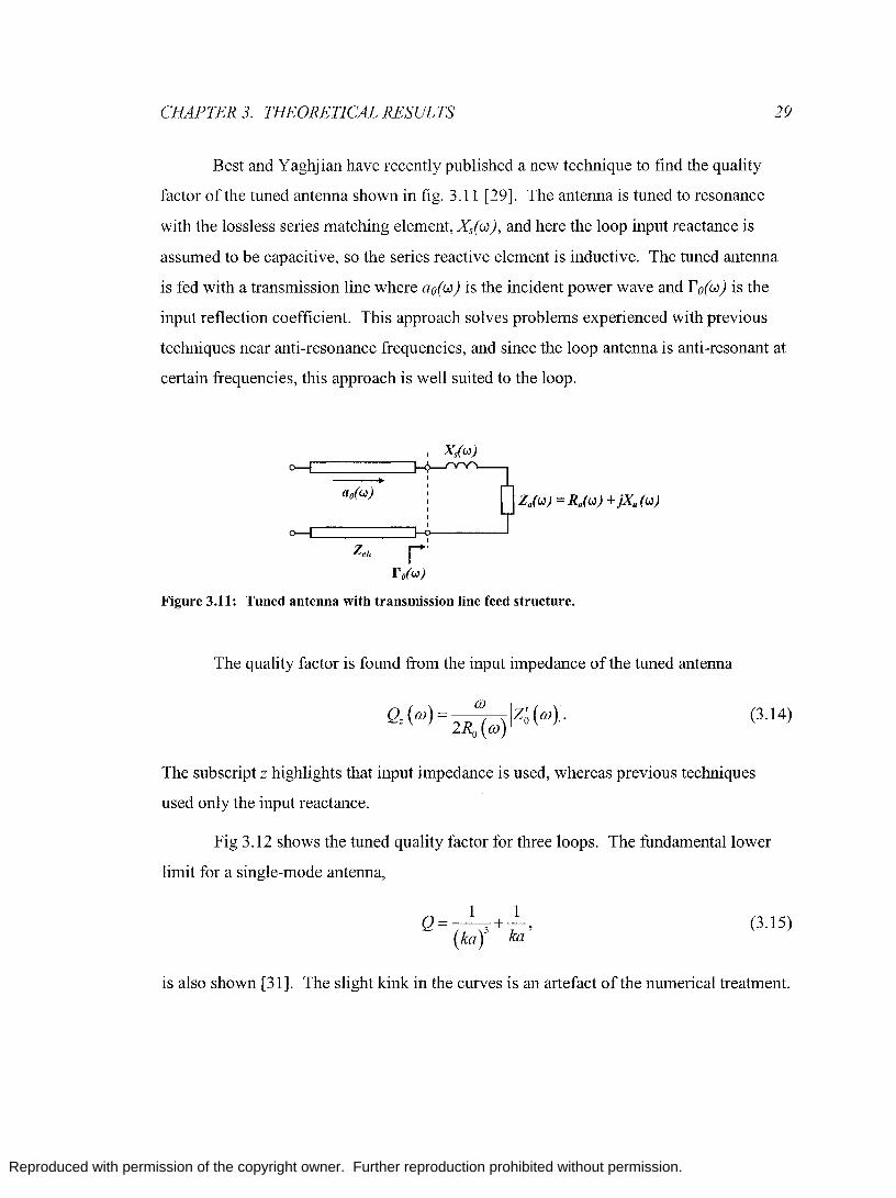
Best and Yaghjian have recently published a new technique to find the quality
factor of the tuned antenna shown in fig. 3.11 [29]. The antenna is tuned to resonance
with the lossless series matching element, )((w), and here the loop input reactance is
assumed to be capacitive, so the series reactive element is inductive. The tuned antenna
is fed with a transmission line where ao(w) is the incident power wave and ro(w) is the
input reflection coefficient. This approach solves problems experienced with previous
techniques near anti-resonance frequencies, and since the loop antenna is anti-resonant at
certain frequencies, this approach is well suited to the loop.
I Xlw)
Figure 3.11: Tuned antenna with transmission line feed structure.
The quality factor is found from the input impedance of the tuned antenna
(3.14)
The subscript z highlights that input impedance is used, whereas previous techniques
used only the input reactance.
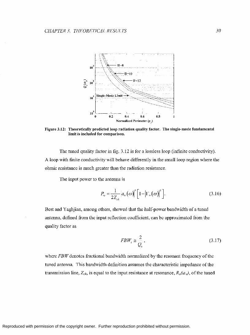
Fig 3.12 shows the tuned quality factor for three loops. The fundamental lower
limit for a single-mode antenna,
(3.15)
is also shown [31]. The slight kink in the curves is an artefact of the numerical treatment.
Reproduced with permission of the copyright owner. Further reproduction prohibited without permission.
CHAPTER 3. THEORETICAL RESULTS
103
'" ~ 2
o;~ 10
101
0 10
0 0.2 0.4 0.6 0.8
Normalized Perimeter (p)
Figure 3.12: Theoretically predicted loop radiation quality factor. The single-mode fundamental limit is included for comparison.
The tuned quality factor in fig. 3.12 is for a lossless loop (infinite conductivity).
30
A loop with finite conductivity will behave differently in the small loop region where the
ohmic resistance is much greater than the radiation resistance.
The input power to the antenna is
(3.16)
Best and Yaghjian, among others, showed that the half-power bandwidth of a tuned
antenna, defined from the input reflection coefficient, can be approximated from the
quality factor as
2 FBW=:::-
Z Qz' (3.17)
where FB W denotes fractional bandwidth normalized by the resonant frequency of the
tuned antenna. This bandwidth definition assumes the characteristic impedance of the
transmission line, Zch, is equal to the input resistance at resonance, Ra(w o), of the tuned
Reproduced with permission of the copyright owner. Further reproduction prohibited without permission.
CHAPTER 3. THEORETICAL RESULTS
antenna, and presents a problem since 50 ohms is the generally accepted RF standard
characteristic impedance.
Fig 3.13 shows the theoretical half-power fractional bandwidth predicted by
(3.17) for three loop antennas.
10°
-I -= 10 :0 .~
'" = .. -2 = 10 -; = .g ... .. .. -3
\.0., 10
10 -4
0 0.2 0.4 0.6 0.8
Normalized Perimetel· (p)
Figure 3.13: Theoretical tuned bandwidth for the three theoretical loop antennas.
The bandwidth of the antennas improves with increasing electrical size, and to a lesser
extent, with increasing loop thickness factor.
31
To illustrate these concepts, consider loop two tuned to resonance at a normalized
perimeter of 0.6, or equivalently 1.43GHz. The predicted input impedance is 110.7 -
j 791.4 ohms with a resonated quality factor of 19.0 . Following (3.17), the predicted half
power bandwidth is 150.5MHz.
To confirm this prediction, fig. 3.14 shows the input reflection coefficient for the
transmission line fed tuned antenna shown in fig. 3.11 with an 87.9 nH series inductor.
This reflection coefficient was calculated numerically using the theoretical input
impedance and simple circuit theory. Two characteristic impedances are considered:
first, equal to the input resistance at resonance, Ra(w o); and second, 50 ohms. The graph
Reproduced with permission of the copyright owner. Further reproduction prohibited without permission.
CHAPTER 3. THEORETICAL RESULTS
is a function of frequency instead of normalized perimeter to facilitate bandwidth
estimates.
U
-1
-2
-3
= -4 "<:I ---" e -s ;~
-6
-7
-8
-9
-10 1 1.1 1.2 1.3 1.4 1.S 1.6 1.7 1.8 1.9 2
Frequency, GHz
Figure 3.14: Input reflection coefficient and bandwidth of the example tuned loop.
The half-power bandwidth for the matched system, estimated from fig. 3.14, is
153MHz - very close to the predicted bandwidth of 150.5 MHz, and is considered the
maximal bandwidth. The second curve shows significantly lower bandwidth as a result
of the mismatch between the transmission line 50 ohm impedance and the input
impedance of the tuned antenna. A matching network is needed to transform the tuned
antenna input resistance to 50 ohms to optimize the bandwidth to that of the tuned
system.
32
The motivation of this thesis is the loop as a compact element, so transmission
line matching schemes are excluded since the required transmission line lengths would be
similar to the overall length of the antenna. Discrete passive elements will introduce
some ohmic loss into the system, but the improvement in power transfer and bandwidth,
as well as the compactness, justify the additional loss.
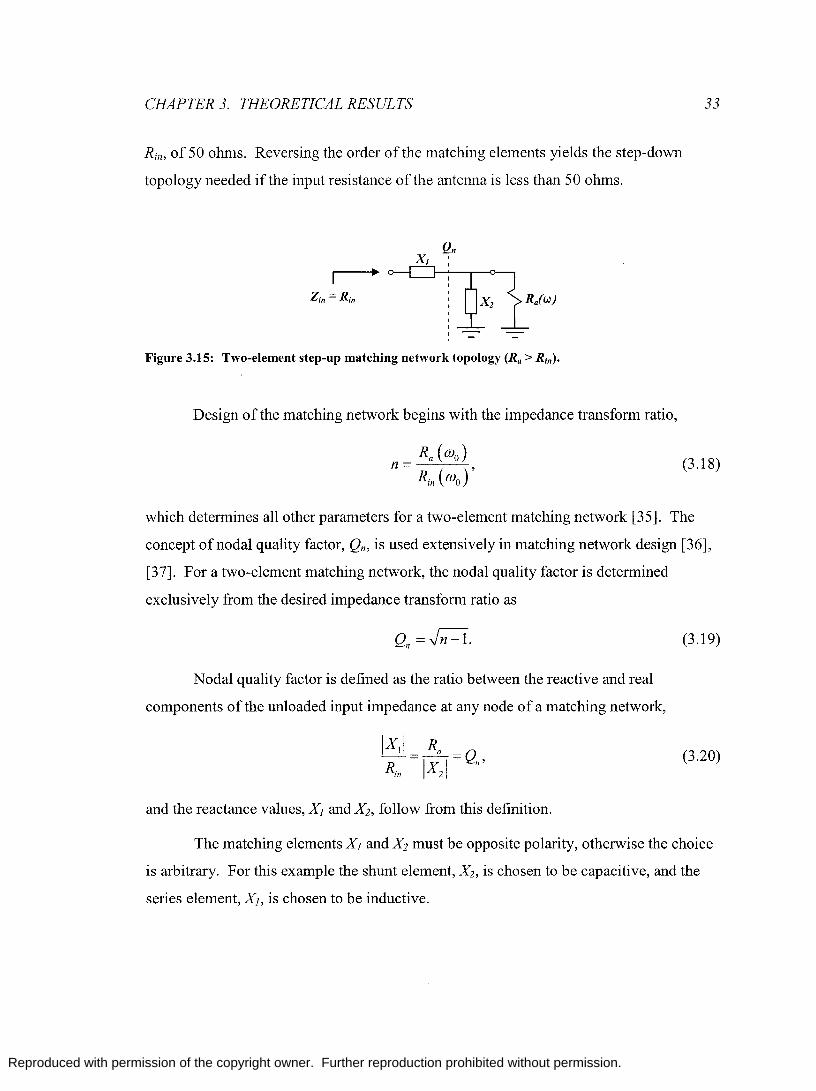
Fig. 3.15 shows the topology for a two-element step-up matching network used
when the input resistance of the antenna, Ra, is greater than the desired input resistance,
Reproduced with permission of the copyright owner. Further reproduction prohibited without permission.
CHAPTER 3. THEORETICAL RESULTS
Rin , of 50 ohms. Reversing the order of the matching elements yields the step-down
topology needed if the input resistance of the antenna is less than 50 ohms.
Figure 3.15: Two-element step-up matching network topology (Ra > Rin).
Design of the matching network begins with the impedance transform ratio,
33
(3.18)
which determines all other parameters for a two-element matching network [35]. The
concept of nodal quality factor, Qn, is used extensively in matching network design [36],
[37). For a two-element matching network, the nodal quality factor is determined
exclusively from the desired impedance transform ratio as
Nodal quality factor is defined as the ratio between the reactive and real
components of the unloaded input impedance at any node of a matching network,
and the reactance values, Xl and X2, follow from this definition.
(3.19)
(3.20)
The matching elements Xl and X2 must be opposite polarity, otherwise the choice
is arbitrary. For this example the shunt element, X2, is chosen to be capacitive, and the
series element, Xl, is chosen to be inductive.

Reproduced with permission of the copyright owner. Further reproduction prohibited without permission.
CHAPTER 3. THEORETICAL RESULTS
Fig. 3.16 shows the composite structure of a tuned antenna plus two-element
matching network.
Zch = 50 ohms
34
Figure 3.16: Composite structure: transmission line feed, two-element matching network, and tuned loop antenna.
The nodal quality factor also directly determines the half-power loaded bandwidth
of a two-element matching network as
(3.21)
By adding additional elements, two at a time, this bandwidth can be increased; however,
the improvement comes with a cost of increased ohmic loss inherently present in discrete
components.
Following the procedure outlined above, the impedance transform ratio for the
tuned loop (loop two) relative to 50 ohms is 2.2, the nodal quality factor is 1.1, and the
required matching elements are a 6.1 nH series inductor and 1.1 pF shunt capacitor.
Note that both the nodal quality factor of the matching network (3.19) and the
quality factor of the tuned antenna in (3.14) are a measure of unloaded quality factor,
both fundamentally defined using the ratio of stored energy to dissipated energy, They
can be directly compared to estimate the bandwidth of the composite structure as shown
in fig. 3.17 for the example loop.
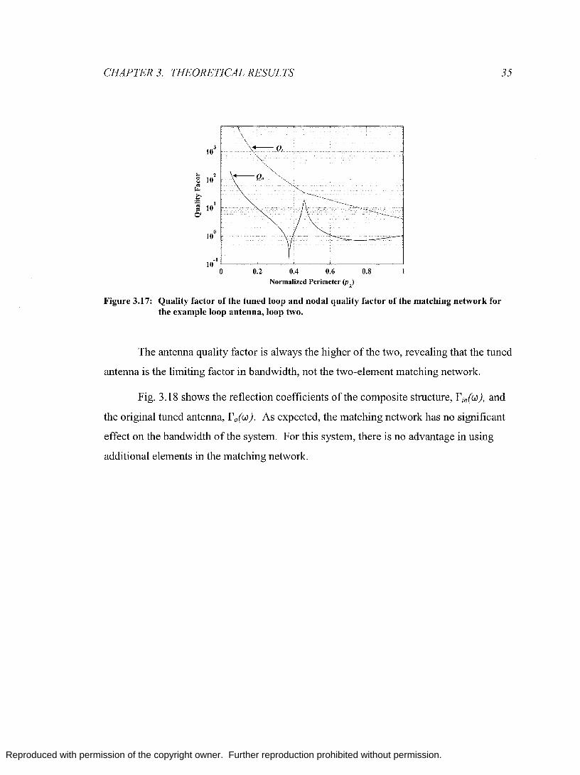
Reproduced with permission of the copyright owner. Further reproduction prohibited without permission.
CHAPTER 3. THEORETICAL RESULTS
... \\
\,+--0. "'~... '
",
+--Qu"""""""""""'"
-1 10 L-____ ~ ____ ~ ____ ~ ____ ~ ____ ~
o 0.2 0.4 0.6 0.8
Normalized Perimeter (p,,>
Figure 3.17: Quality factor of the tuned loop and nodal quality factor of the matching network for the example loop antenna, loop two.
35
The antenna quality factor is always the higher of the two, revealing that the tuned
antenna is the limiting factor in bandwidth, not the two-element matching network.
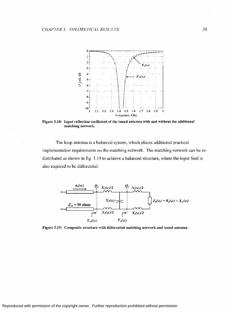
Fig. 3.18 shows the reflection coefficients of the composite structure, rin(w), and
the original tuned antenna, ro(w). As expected, the matching network has no significant
effect on the bandwidth of the system. For this system, there is no advantage in using
additional elements in the matching network.
Reproduced with permission of the copyright owner. Further reproduction prohibited without permission.
CHAPTER 3, THEORETICAL RESULTS
0
-1
-2
-3
= -4 "0 -...!:.
~ -5 ;:~
-6
-7
-8
-9
-10 1 1.1 1.2 1.3 1.4 1.5 1,6 1. 7 1.8 1.9 2
F,'equeucy, GHz
Figure 3.18: Input reflection coefficient of the tuned antenna with and without the additional matching network.
36
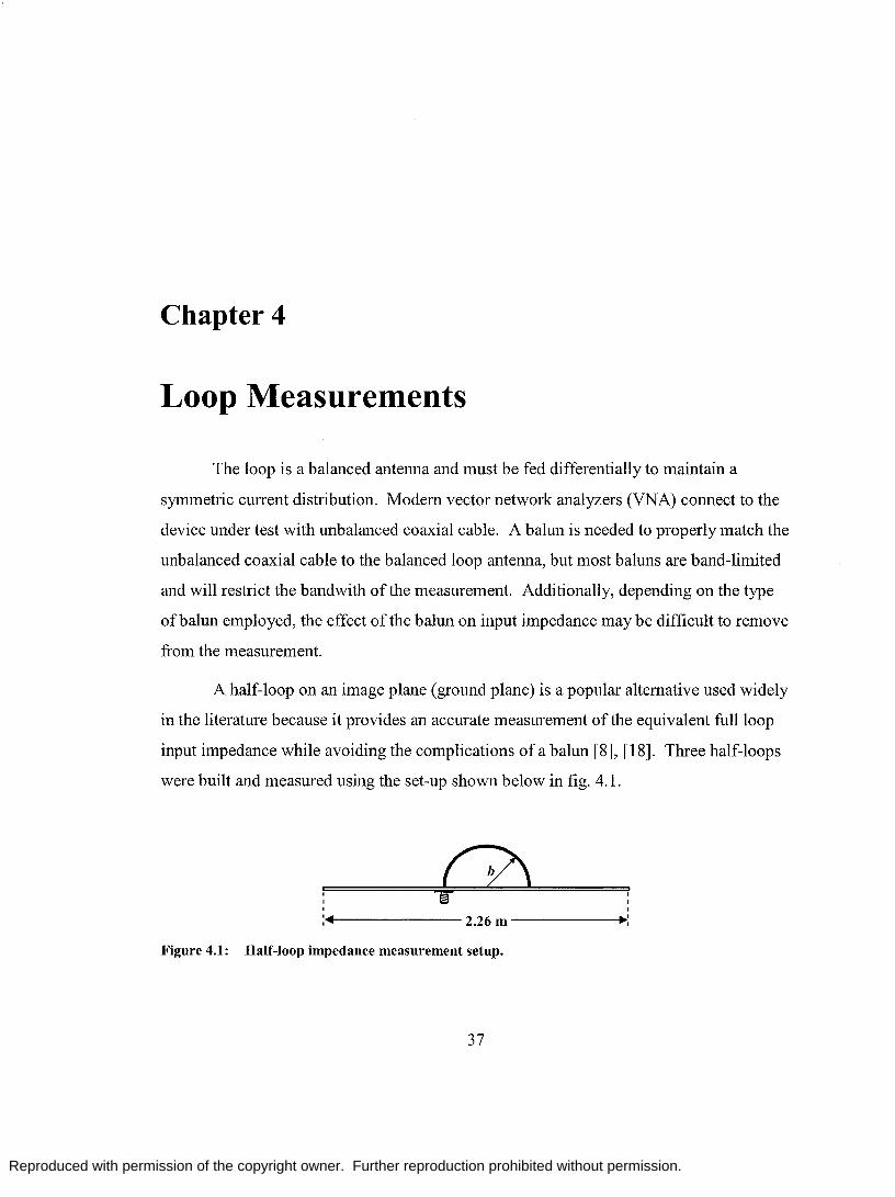
The loop antenna is a balanced system, which places additional practical
implementation requirements on the matching network. The matching network can be re
distributed as shown in fig, 3.19 to achieve a balanced structure, where the input feed is
also required to be differential.
ao(w) Qn Xdw)/2 Qz Xlw)/2 I I
Za(w) = Ra(w) + xa (w) Zch = 50 ohms
I Xj(w)/2 I
Xlw)/2
" " fin(w) fo(w)
Figure 3.19: Composite structure with differential matching network and tuned antenna.
Reproduced with permission of the copyright owner. Further reproduction prohibited without permission.
Chapter 4
Loop Measurements
The loop is a balanced antenna and must be fed differentially to maintain a
symmetric current distribution. Modem vector network analyzers (VNA) connect to the
device under test with unbalanced coaxial cable. A balun is needed to properly match the
unbalanced coaxial cable to the balanced loop antenna, but most baluns are band-limited
and will restrict the bandwith of the measurement. Additionally, depending on the type
of balun employed, the effect of the balun on input impedance maybe difficult to remove
from the measurement.
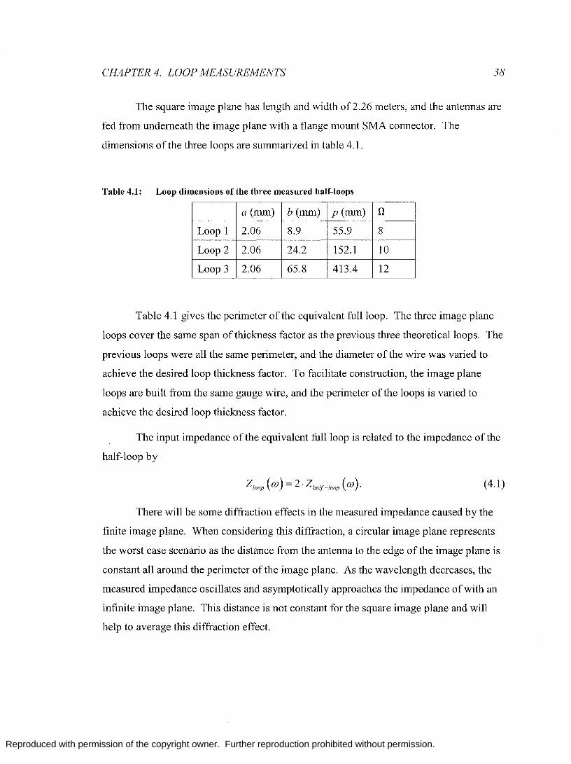
A half-loop on an image plane (ground plane) is a popular alternative used widely
in the literature because it provides an accurate measurement of the equivalent full loop
input impedance while avoiding the complications of a balun [8], [18]. Three half-loops
were built and measured using the set-up shown below in fig. 4.1.
~ , , : .. 2.26m .' ,
Figure 4.1: Half-loop impedance measurement setup.
37
Reproduced with permission of the copyright owner. Further reproduction prohibited without permission.
CHAPTER 4. LOOP MEASUREMENTS 38
The square image plane has length and width of 2.26 meters, and the antennas are
fed from underneath the image plane with a flange mount SMA connector. The
dimensions of the three loops are summarized in table 4.1.
Table 4.1: Loop dimensions of the three measured half-loops
a (mm) b(mm) p(mm) n Loop 1 2.06 8.9 55.9 8
Loop 2 2.06 24.2 152.1 10
Loop 3 2.06 65.8 413.4 12
Table 4.1 gives the perimeter of the equivalent full loop. The three image plane
loops cover the same span of thickness factor as the previous three theoretical loops. The
previous loops were all the same perimeter, and the diameter of the wire was varied to
achieve the desired loop thickness factor. To facilitate construction, the image plane
loops are built from the same gauge wire, and the perimeter of the loops is varied to
achieve the desired loop thickness factor.
The input impedance of the equivalent full loop is related to the impedance of the
half-loop by
Zloop (OJ) = 2· Zha/f -loop (OJ). (4.1)
There will be some diffraction effects in the measured impedance caused by the
finite image plane. When considering this diffraction, a circular image plane represents
the worst case scenario as the distance from the antenna to the edge of the image plane is
constant all around the perimeter of the image plane. As the wavelength decreases, the
measured impedance oscillates and asymptotically approaches the impedance of with an
infinite image plane. This distance is not constant for the square image plane and will
help to average this diffraction effect.
Reproduced with permission of the copyright owner. Further reproduction prohibited without permission.
CHAPTER 4. LOOP MEASUREMENTS
The following VNA settings were used to obtain accurate measurements of the
untuned loops: 10 dBm output power, 10kHz IF bandwidth, and time averaging factor
of 50. These settings maximise the signal to noise ratio (SNR) of the measurements.
4.1 Measured Impedances
39
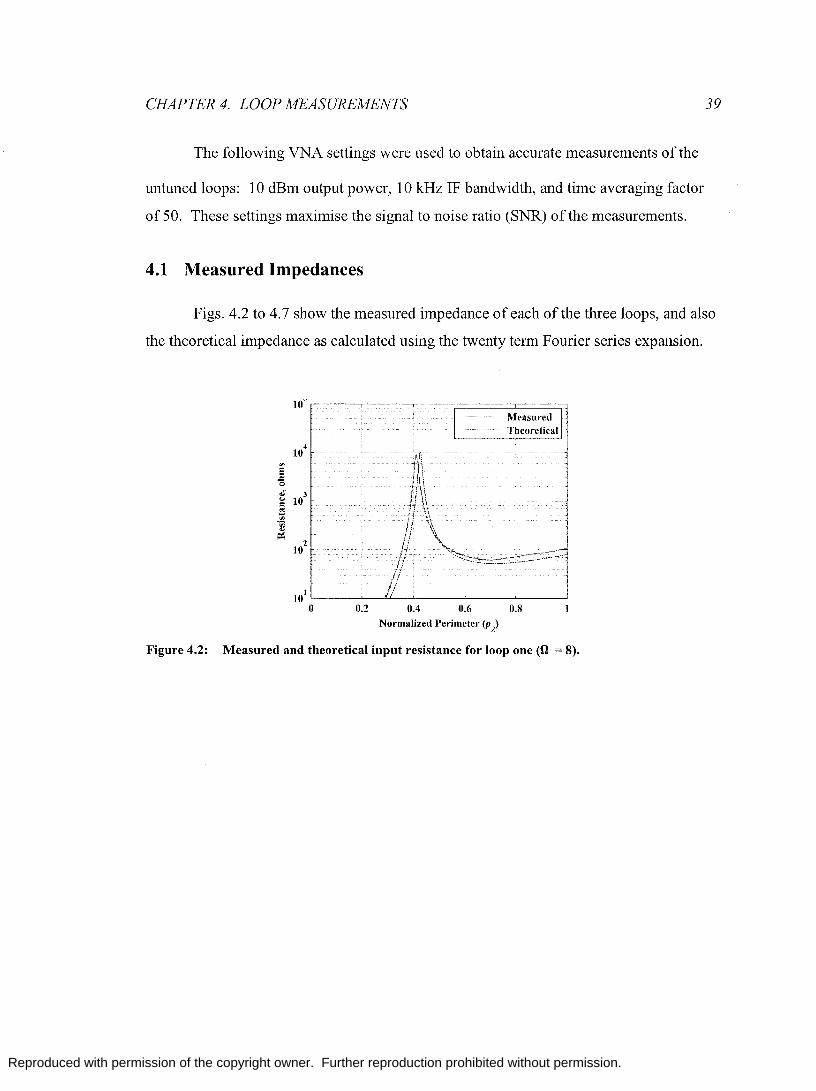
Figs. 4.2 to 4.7 show the measured impedance of each of the three loops, and also
the theoretical impedance as calculated using the twenty term Fourier series expansion.
10--
4 10
'" 5 .: 0
,; 10
3
" = ;s .~ ... ;:::
102
101
0 0.2 0.4
..................... .... Measured
------------------ Theoretical
0.6 0.8
Normalized Perimeter (p)
Figure 4.2: Measured and theoretical input resistance for loop one (U = 8).
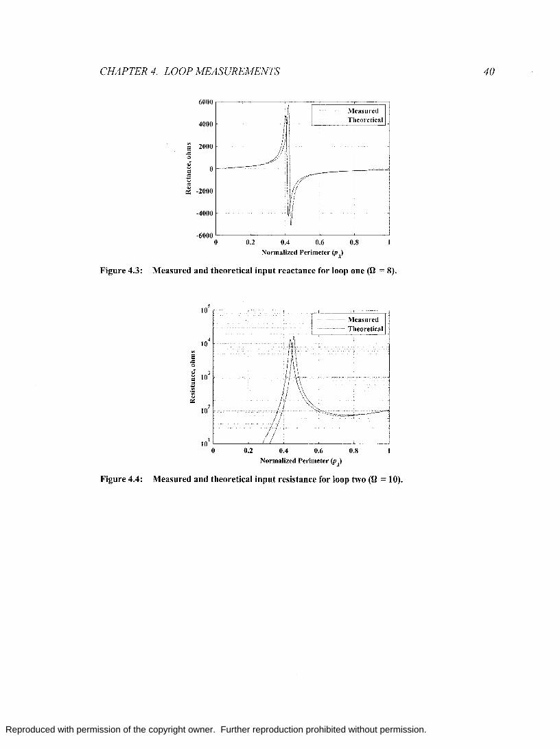
Reproduced with permission of the copyright owner. Further reproduction prohibited without permission.
CHAPTER 4, LOOP MEASUREMENTS
6000
4000
'" 2000 2 .c 0
.s '" 0 CI 1: '" '" 0;
-2000 ~
-4000
-6000 0 0,2 0,4 0,6
Normalized Perimeter' (p..>
Measured Th eoretical
O.S
Figure 4.3: Measured and theoretical input reactance for loop one (U = 8).
5 10
104
8 .c 0
.s 10
3 '" = ~ 'en 0;
~
102
101
0 0.2 0,4
1
_-- Measured I ------------------ Theoretical I
0.6 O,S
Normalized Perimeter (p..>
Figure 4.4: Measured and theoretical input resistance for loop two (U = 10).
40
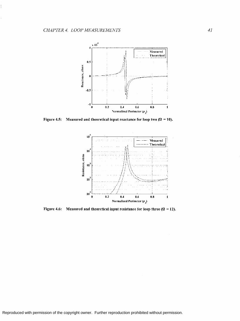
Reproduced with permission of the copyright owner. Further reproduction prohibited without permission.
CHAPTER 4. LOOP MEASUREMENTS
'" E -= 0
.r " = .5 " .. ..
CI::
4 X 10
1 ~·-·---r··-----;:=· =====:;l
0.5
0
-0.5
-1 0 0.2 0.4
._._ .. _ .... Measured ... Theoretical
0.6 0.8
Normalized Perimeter (p)
Figure 4.5: Measured and theoretical input reactance for loop two (fl = 10).
5 10
104
e -= 0
.r 3 " 10 = .5 '" .;; ..
CI:: 2
10
101
0 0.2 0.4
Measured .................. Theoretical
0.6 0.8
Normalized Perimeter (p .. )
Figure 4.6: Measured and theoretical input resistance for loop three (fl = 12).
41
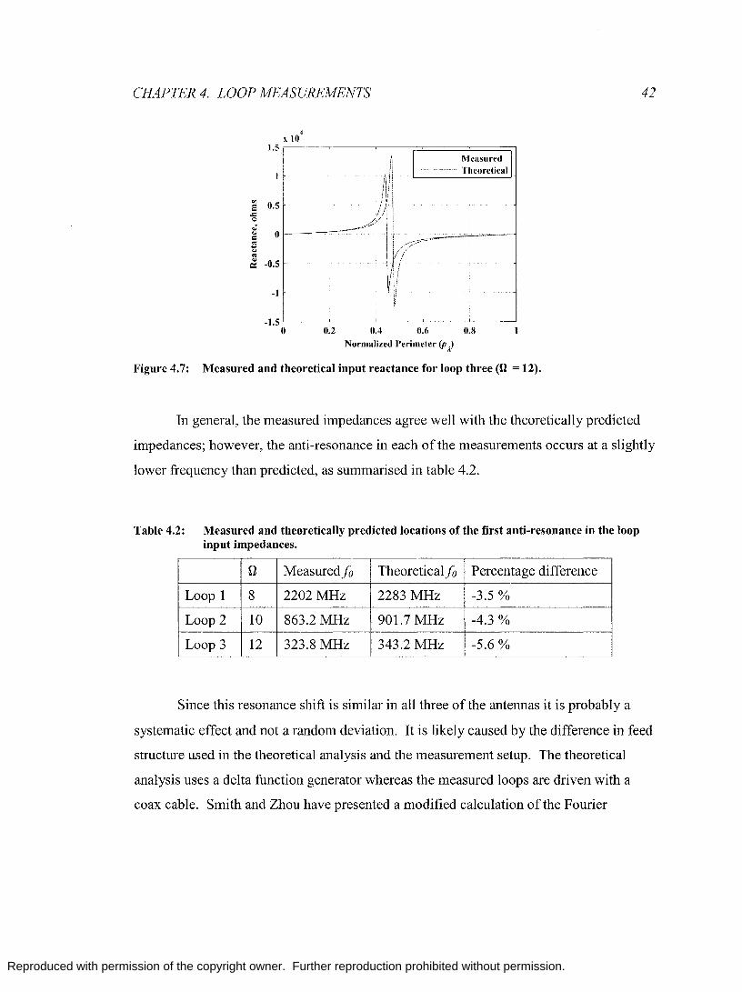
Reproduced with permission of the copyright owner. Further reproduction prohibited without permission.
CHAPTER 4. LOOP MEASUREMENTS
5 .c 0
or " = -5 " '" " 0:
4 X 10
1.5 r----~--~------;::=======il
I ----------- ~he::;:~~:all
0.5
0
-0.5
-1
-1.5 0 0.2 0.4 0.6 0.8
Normalized Perimeter (p)
Figure 4.7: Measured and theoretical input reactance for loop three (U = 12).
42
In general, the measured impedances agree well with the theoretically predicted
impedances; however, the anti-resonance in each of the measurements occurs at a slightly
lower frequency than predicted, as summarised in table 4.2.
Table 4.2: Measured and theoretically predicted locations of the first anti-resonance in the loop input impedances.
n Measuredfo Theoretical fa Percentage difference
Loop 1 8 2202 MHz 2283 MHz -3.5 %
Loop 2 10 863.2 MHz 901.7 MHz -4.3 %
Loop 3 12 323.8 MHz 343.2 MHz -5.6 %
Since this resonance shift is similar in all three of the antennas it is probably a
systematic effect and not a random deviation. It is likely caused by the difference in feed
structure used in the theoretical analysis and the measurement setup. The theoretical
analysis uses a delta function generator whereas the measured loops are driven with a
coax cable. Smith and Zhou have presented a modified calculation of the Fourier
Reproduced with permission of the copyright owner. Further reproduction prohibited without permission.
CHAPTER 4. LOOP MEASUREMENTS 43
coefficients based on this type of feed structure that could potentially yield more accurate
agreement [18]; however, this is not pursued further here.
4.2 Radiation Efficiency Measurements
A Wheeler cap was used to measure the radiation efficiency of two of the loop
antennas. This approach was originally proposed by Wheeler, and several well known
authors have evaluated this technique both theoretically and experimentally [40], [41],
[42]. The consensus amongst these papers is the technique is generally easier to
implement than alternative approaches, and it is well suited to comparing relative
efficiencies, but is not highly accurate for measuring absolute efficiency.
The antenna radiation efficiency is determined by first measuring the input
resistance of the antenna in free-space, R I . The antenna is then enclosed in a conductive
chamber and the input resistance is measured again, R2. Ideally, the conductive chamber
returns all radiating power to the antenna, removing the radiation resistance from the
second measurement, and the radiation efficiency is found as
(4.2)
The Wheeler cap must not distort the current distribution or near-fields of the
antenna. Accordingly, Wheeler suggested the distance between the antenna and cap must
be at least one radiansphere,
A r=-
2tr' (4.3)
generally accepted as the boundary between the near-fields and far-fields of an antenna.
The shape of the cap is not critical as long as this condition is met.
The Wheeler cap built to measure the radiation efficiency of the half-loop
antennas is shown in fig. 4.8. It was constructed by building a cardboard box of
appropriate size and then lining the box with aluminium foil. It was not expected to
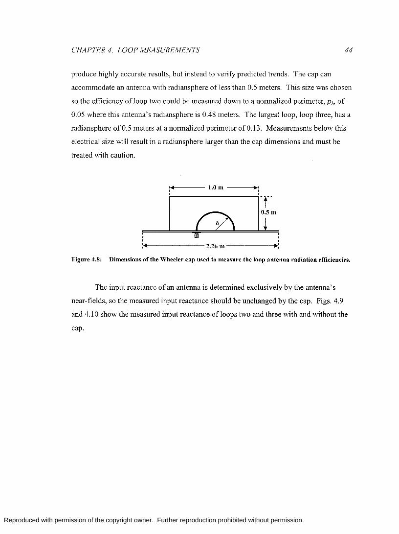
Reproduced with permission of the copyright owner. Further reproduction prohibited without permission.
CHAPTER 4. LOOP MEASUREMENTS 44
produce highly accurate results, but instead to verify predicted trends. The cap can
accommodate an antenna with radiansphere of less than 0.5 meters. This size was chosen
so the efficiency of loop two could be measured down to a normalized perimeter, p", of
0.05 where this antenna's radiansphere is 0.48 meters. The largest loop, loop three, has a
radiansphere of 0.5 meters at a normalized perimeter of 0.13. Measurements below this
electrical size will result in a radiansphere larger than the cap dimensions and must be
treated with caution.
' ...... ---- 1.0 m ---•• ' , , , ,
, , , , , , : ...... ------- 2.26 m ------+'.:
Figure 4.8: Dimensions of the Wheeler cap used to measure the loop antenna radiation efficiencies.
The input reactance of an antenna is determined exclusively by the antenna's
near-fields, so the measured input reactance should be unchanged by the cap. Figs. 4.9
and 4.10 show the measured input reactance of loops two and three with and without the
cap.
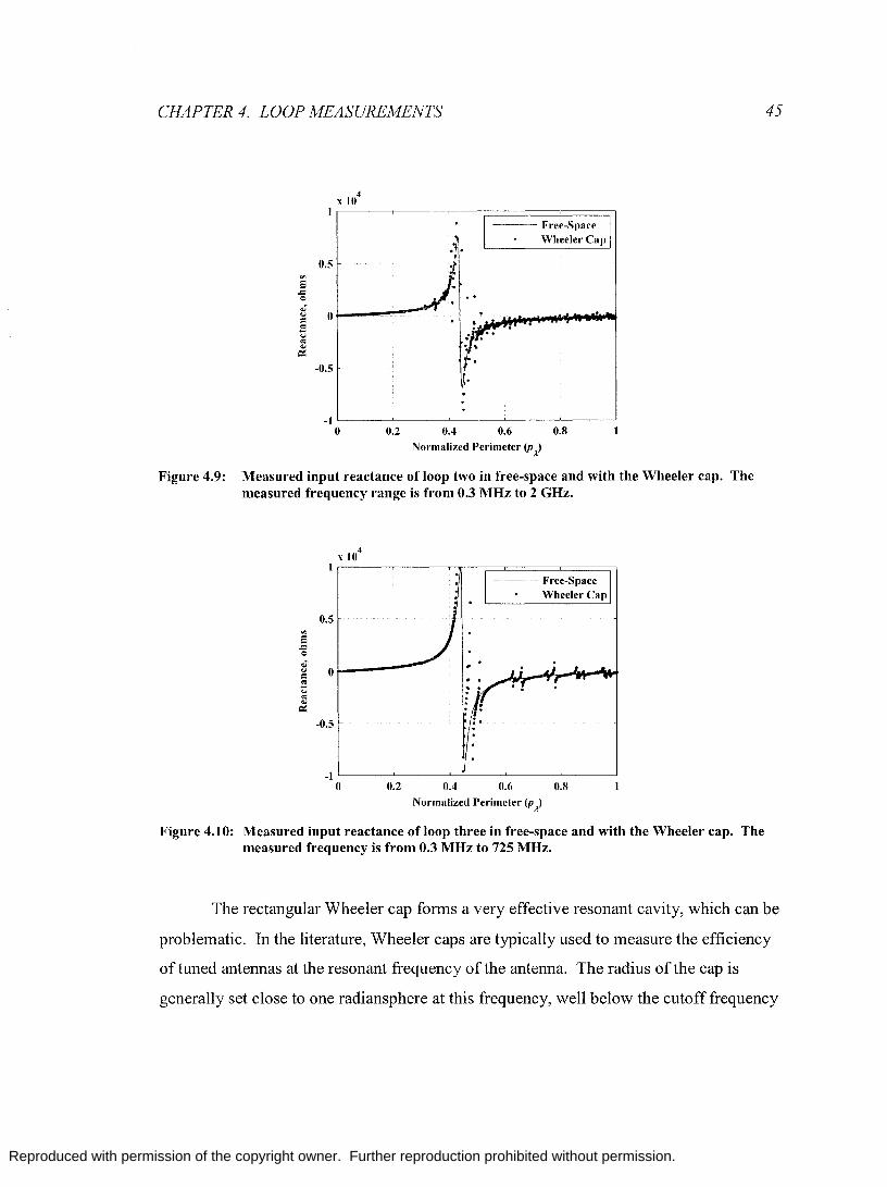
Reproduced with permission of the copyright owner. Further reproduction prohibited without permission.
CHAPTER 4. LOOP MEASUREMENTS
I
0.5 'I>
S .c 0
oS ... 0 = Zl ... " ...
.z:: -0.5
-1
X 10 4
0 0.2 0.4
--- Free-Space Wheeler Cap
0.6 0.8
Normalized Perimeter (p}
Figure 4.9: Measured input reactance of loop two in free-space and with the Wheeler cap. The measured frequency range is from 0.3 MHz to 2 GHz.
X 10 4
1 --- Free-Space
Wheeler Cap
0.5 'I>
S .c 0
oS '"' 0 = " .... '"' " ...
.z:: -0.5
-1 0 0.2 0.4 0.6 0.8
Normalized Perimeter (p..>
Figure 4.10: Measured input reactance ofloop three in free-space and with the Wheeler cap. The measured frequency is from 0.3 MHz to 725 MHz.
45
The rectangular Wheeler cap forms a very effective resonant cavity, which can be
problematic. In the literature, Wheeler caps are typically used to measure the efficiency
of tuned antennas at the resonant frequency of the antenna. The radius of the cap is
generally set close to one radiansphere at this frequency, well below the cutoff frequency
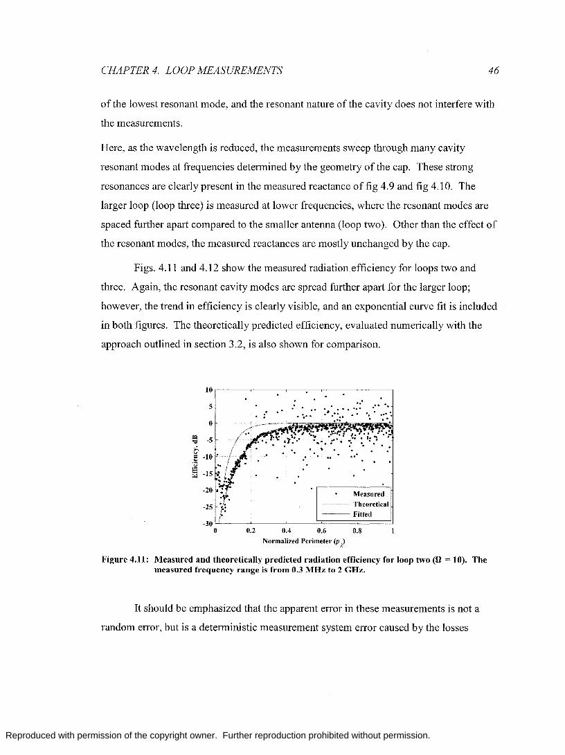
Reproduced with permission of the copyright owner. Further reproduction prohibited without permission.
CHAPTER 4. LOOP MEASUREMENTS 46
of the lowest resonant mode, and the resonant nature of the cavity does not interfere with
the measurements.
Here, as the wavelength is reduced, the measurements sweep through many cavity
resonant modes at frequencies determined by the geometry ofthe cap. These strong
resonances are clearly present in the measured reactance of fig 4.9 and fig 4.10. The
larger loop (loop three) is measured at lower frequencies, where the resonant modes are
spaced further apart compared to the smaller antenna (loop two). Other than the effect of
the resonant modes, the measured reactances are mostly unchanged by the cap.
Figs. 4.11 and 4.12 show the measured radiation efficiency for loops two and
three. Again, the resonant cavity modes are spread further apart for the larger loop;
however, the trend in efficiency is clearly visible, and an exponential curve fit is included
in both figures. The theoretically predicted efficiency, evaluated numerically with the
approach outlined in section 3.2, is also shown for comparison.
10
5
0
>:'1 -5 ." ,:; ... = " .;;
!;::i .... -15 "'"
-20
-25
-30 0 0.2
.. . : .. .....
. , . . .
...... . . . .... .'
Measured --- Theoretical
---Fitted
0.4 0.6 0.8
Normalized Perimeter (p)
Figure 4.11: Measured and theoretically predicted radiation efficiency for loop two (U = 10). The measured frequency range is from 0.3 MHz to 2 GHz.
It should be emphasized that the apparent error in these measurements is not a
random error, but is a deterministic measurement system error caused by the losses

Reproduced with permission of the copyright owner. Further reproduction prohibited without permission.
CHAPTER 4. LOOP MEASUREMENTS 47
(ohmic and radiation leakage) of the Wheeler cap. The measurements were taken several
times and the scattered data points were the same each time.
" 5 . : '; /I, .*
Measured
:a -5
;. ~'. . //···· .. · .. · ..... ::n~~i\·~~~·
,/ ~.': ", • I ,-./Jri4r· " , .. , -', ; ", , // ". ~ : .. " ". . ..
,/ / :: . " ,. J .....
•• f !. -20 ~,
i~.
o
;;:., '" ~ -10
'0:; !.: ~ -15
. ................... Theoretical -25 '
Fitted
-30 U,L_'--__ '---'========='l o 0.2 0.4 0.6 0.8
Normalized Perimeter (p.<)
Figure 4.12: Measured and theoretically predicted radiation efficiency for loop three (U = 12). The measured frequency is from 0.3 MHz to 725 MHz.
The measured efficiency of both loops is lower than expected at intermediate
electrical sizes, but asymptotically approaches the predicted efficiency with increasing
electrical size. The Wheeler cap will have ohmic losses and radiation losses at the seams
of the aluminium foil and at the boundary between the ground plane and the cap.
Following Smith [42], these losses, Rc, will degrade the measured efficiency,
R -R Rad Cap , RRad + Ro.
(4.4)
where Rn and RRad are the antenna ohmic loss and antenna radiation resistance
respectively. As the electrical size increases the radiation resistance becomes much
larger than both the antenna ohmic loss and cap loss, and the efficiency approaches unity.
Fig. 4.13 shows the fitted measurement results and the theoretical efficiency.
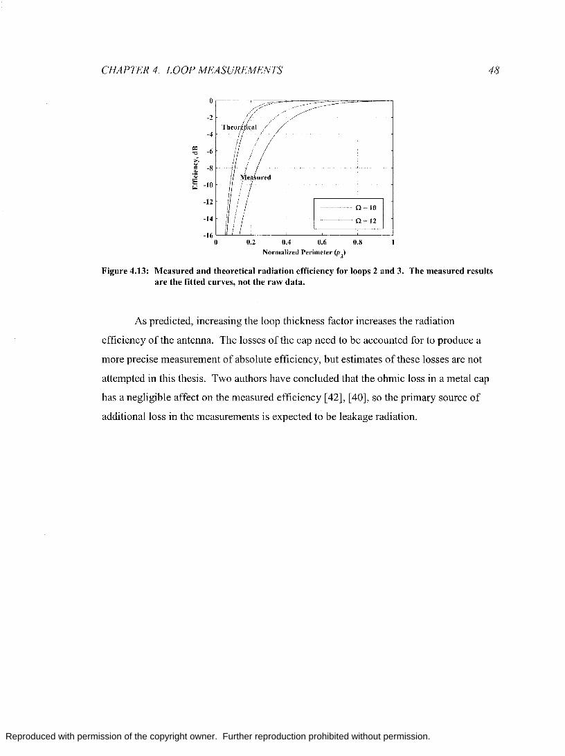
Reproduced with permission of the copyright owner. Further reproduction prohibited without permission.
CHAPTER 4. LOOP MEASUREMENTS 48
...... ······0= 10
---0=12
0.2 0.4 0.6 0.8
Normalized Perimeter (p.<)
Figure 4.13: Measured and theoretical radiation efficiency for loops 2 and 3. The measured results are the fitted curves, not the raw data.
As predicted, increasing the loop thickness factor increases the radiation
efficiency of the antenna. The losses of the cap need to be accounted for to produce a
more precise measurement of absolute efficiency, but estimates of these losses are not
attempted in this thesis. Two authors have concluded that the ohmic loss in a metal cap
has a negligible affect on the measured efficiency [42], [40], so the primary source of
additional loss in the measurements is expected to be leakage radiation.
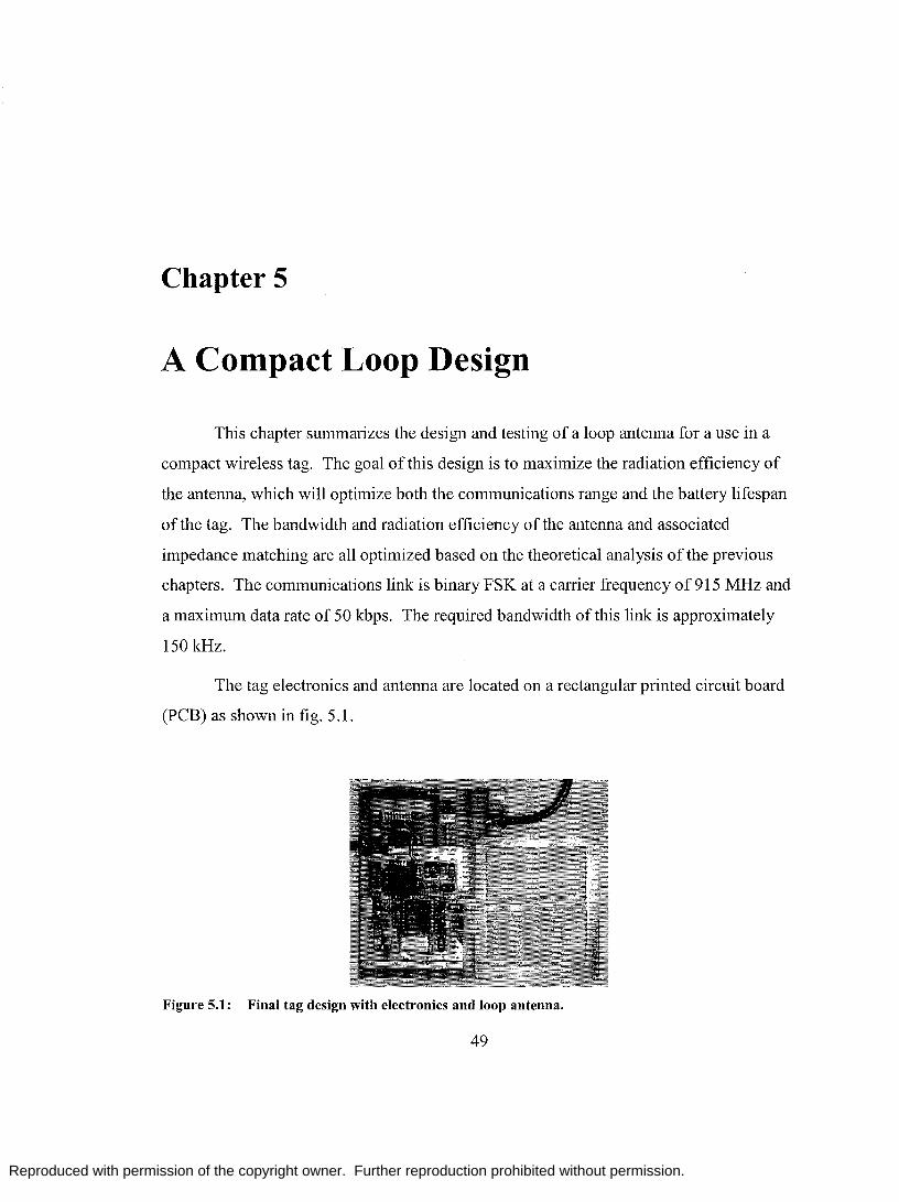
Reproduced with permission of the copyright owner. Further reproduction prohibited without permission.
Chapter 5
A Compact Loop Design
This chapter summarizes the design and testing of a loop antenna for a use in a
compact wireless tag. The goal of this design is to maximize the radiation efficiency of
the antenna, which will optimize both the communications range and the battery lifespan
of the tag. The bandwidth and radiation efficiency of the antenna and associated
impedance matching are all optimized based on the theoretical analysis of the previous
chapters. The communications link is binary FSK at a carrier frequency of 915 MHz and
a maximum data rate of 50 kbps. The required bandwidth of this link is approximately
150 kHz.
The tag electronics and antenna are located on a rectangular printed circuit board
(PCB) as shown in fig. 5.1.
Figure 5.1: Final tag design with electronics and loop antenna.
49
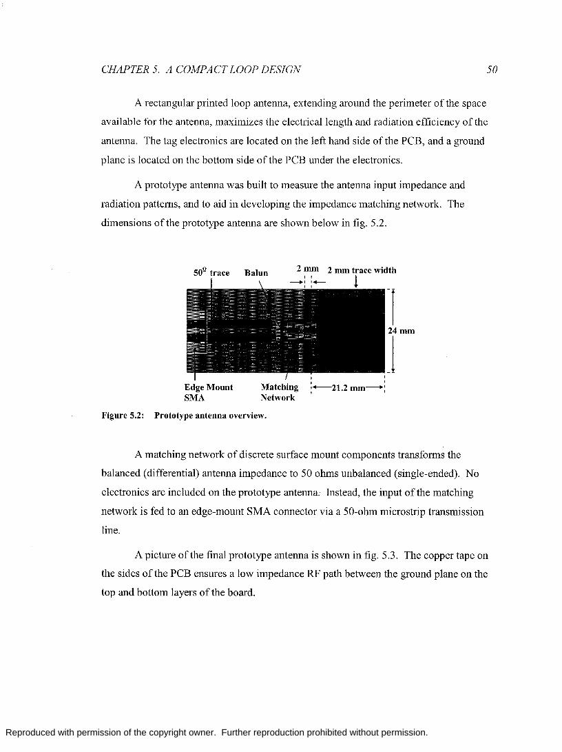
Reproduced with permission of the copyright owner. Further reproduction prohibited without permission.
CHAPTER 5. A COMPACT LOOP DESIGN 50
A rectangular printed loop antenna, extending around the perimeter of the space
available for the antenna, maximizes the electrical length and radiation efficiency of the
antenna. The tag electronics are located on the left hand side of the PCB, and a ground
plane is located on the bottom side of the PCB under the electronics.
A prototype antenna was built to measure the antenna input impedance and
radiation patterns, and to aid in developing the impedance matching network. The
dimensions of the prototype antenna are shown below in fig. 5.2.
50° trace Balun 2 mm 2 mm trace width
Edge Mount SMA
Matching Network
Figure 5.2: Prototype antenna overview.
! -1 24mm
J I I I I
:-21.2mm-:
A matching network of discrete surface mount components transforms the
balanced (differential) antenna impedance to 50 ohms unbalanced (single-ended). No
electronics are included on the prototype antenna. Instead, the input of the matching
network is fed to an edge-mount SMA connector via a 50-ohm microstrip transmission
line.
A picture of the final prototype antenna is shown in fig. 5.3. The copper tape on
the sides of the PCB ensures a low impedance RF path between the ground plane on the
top and bottom layers of the board.
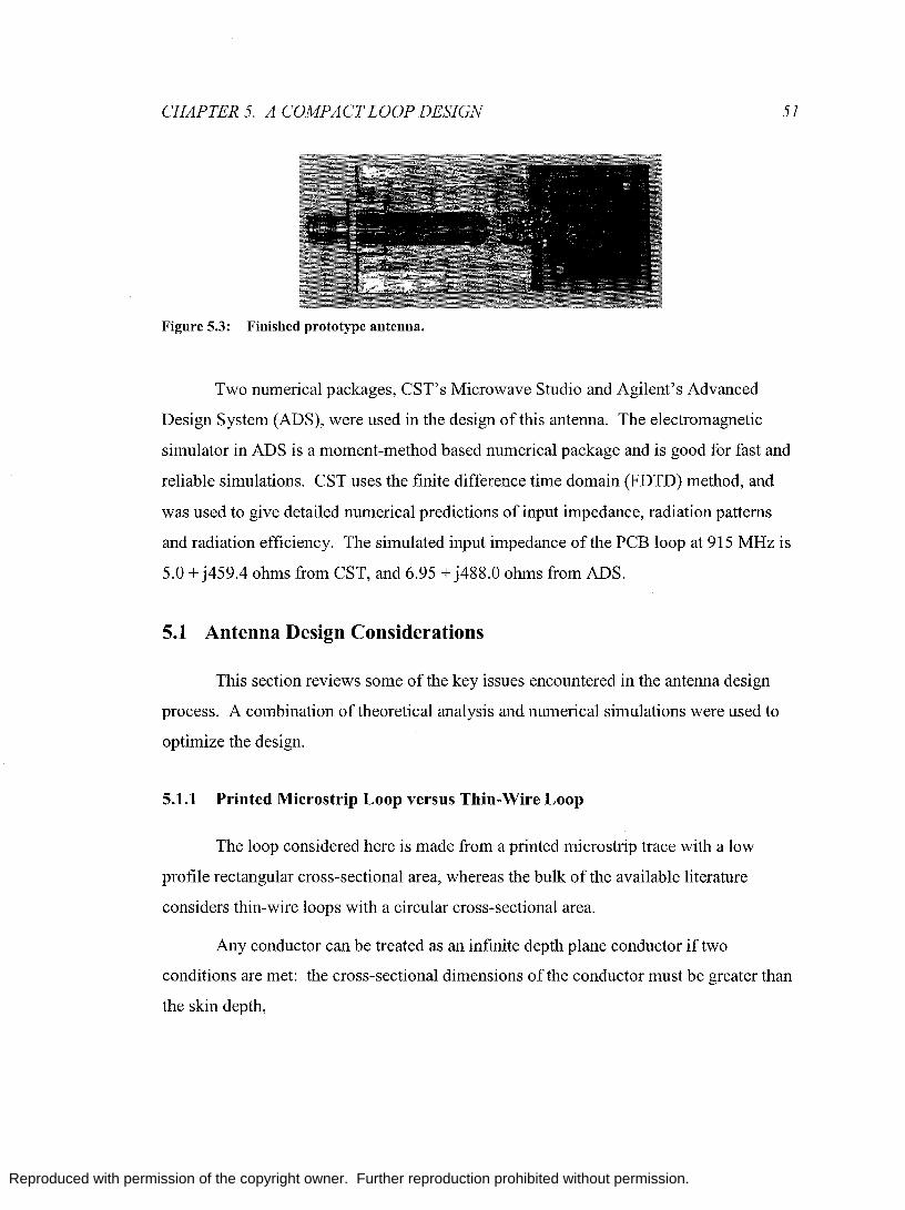
Reproduced with permission of the copyright owner. Further reproduction prohibited without permission.
CHAPTER 5. A COMPACT LOOP DESIGN 51
Figure 5.3: Finished prototype antenna.
Two numerical packages, CST's Microwave Studio and Agilent's Advanced
Design System (ADS), were used in the design of this antenna. The electromagnetic
simulator in ADS is a moment-method based numerical package and is good for fast and
reliable simulations. CST uses the finite difference time domain (FDTD) method, and
was used to give detailed numerical predictions of input impedance, radiation patterns
and radiation efficiency. The simulated input impedance of the PCB loop at 915 MHz is
5.0 + j459.4 ohms from CST, and 6.95 + j488.0 ohms from ADS.
5.1 Antenna Design Considerations
This section reviews some of the key issues encountered in the antenna design
process. A combination of theoretical analysis and numerical simulations were used to
optimize the design.
5.1.1 Printed Microstrip Loop versus Thin-Wire Loop
The loop considered here is made from a printed microstrip trace with a low
profile rectangular cross-sectional area, whereas the bulk ofthe available literature
considers thin-wire loops with a circular cross-sectional area.
Any conductor can be treated as an infinite depth plane conductor if two
conditions are met: the cross-sectional dimensions ofthe conductor must be greater than
the skin depth,
Reproduced with permission of the copyright owner. Further reproduction prohibited without permission.
CHAPTER 5. A COMPA CT LOOP DESIGN 52
(5.1)
calculated for copper at 915 MHz, and the current must be uniformly distributed around
the cross-section ofthe conductor [5]. The thickness of the PCB trace (20 J-Lm) is larger
than the skin depth by a factor of 10, so the first condition is satisfied. The loop thickness
factor, 0, can be estimated for this loop as
(5.2)
where p is the mean perimeter of the loop (82.4 mm) and w is the trace width (2 mm). As
previously shown, the assumption of uniform current distribution for this thickness factor
is marginal; however, the resulting error is not significant.
With both conditions satisfied, the internal impedance of an electrically small
structure is defined as the contribution to the input impedance from fields within the
conductor [5],
Z = -+- x-( 1 j) I
S ao ao weff
' (5.3)
where I is the length of the conductor, and the effective width, weff' is illustrated below in
fig. 5.4.
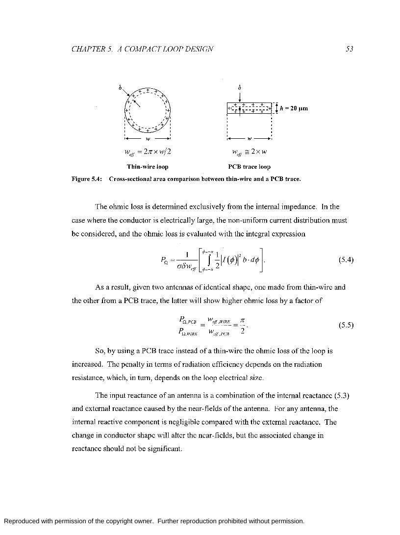
Reproduced with permission of the copyright owner. Further reproduction prohibited without permission.
CHAPTER 5. A COMPACT LOOP DESIGN
W ejf = 27r X w/2
Thin-wire loop
, , , , , ,-w---,
W ejf == 2xw
PCB trace loop
Figure 5.4: Cross-sectional area comparison between thin-wire and a PCB trace.
53
The ohmic loss is detennined exclusively from the internal impedance. In the
case where the conductor is electrically large, the non-unifonn current distribution must
be considered, and the ohmic loss is evaluated with the integral expression
(5.4)
As a result, given two antennas of identical shape, one made from thin-wire and
the other from a PCB trace, the latter will show higher ohmic loss by a factor of
PO,PCB Wejf,WfRE 7r
PO,WIRE Wejf,PCB 2
So, by using a PCB trace instead of a thin-wire the ohmic loss of the loop is
increased. The penalty in tenns of radiation efficiency depends on the radiation
resistance, which, in tum, depends on the loop electrical size.
(5.5)
The input reactance of an antenna is a combination ofthe internal reactance (5.3)
and external reactance caused by the near-fields of the antenna. For any antenna, the
internal reactive component is negligible compared with the external reactance. The
change in conductor shape will alter the near-fields, but the associated change in
reactance should not be significant.

Reproduced with permission of the copyright owner. Further reproduction prohibited without permission.
CHAPTER 5. A COMPACT LOOP DESIGN 54
5.1.2 Optimum PCB Trace Width
Section 3.2 showed that small-loop theory can be used to estimate the radiation
efficiency of an electrically large loop. The small loop radiation resistance,
(5.6)
is proportional to the enclosed area of the loop,
A = (21.2-2w)(24-2w), (5.7)
where w is the width of the trace and all dimensions are given in mm. The area reserved
for the antenna is limited to 24 mm by 21.2 mm, as shown in fig. 5.5, so the trace width
can only be increased on the inside edge of the loop.
L ,,~
t w
GroundPlane ;- 24mm
:+~ -------+i.: 21.2 mm
Figure 5.5: PCB antenna dimensional restrictions.
As the width of the trace is increased, the enclosed area is reduced, and radiation
efficiency,
(5.8)
is also reduced.
The small loop ohmic resistance is found from the real part of(5.3).

Reproduced with permission of the copyright owner. Further reproduction prohibited without permission.
CHAPTER 5. A COMPACT LOOP DESIGN 55
R = _1_ Pave n m5 2w '
(5.9)
where the effective width, Wejf, is replaced with the trace width, w, as shown in fig. 5.4.
The average perimeter of the loop is given by
Pave =2(21.2+24)-4w. (5.10)
So, increasing the trace width will also reduce the ohmic losses of the antenna, improving
the radiation efficiency.
Section 3.1 showed that current begins to concentrate on the inside edge of the
loop as the thickness factor increases. The small loop formulations used above assume a
uniform circular cross-sectional current distribution, and become less accurate with
increasing trace width, but still provide useful insight into the electromagnetic
mechanisms.
There is a trade-off in optimizing the trace width. Increasing the width reduces
ohmic loss, improving the radiation efficiency, but at the same time the enclosed area is
reduced, degrading the radiation efficiency. Ultimately, the optimum trace width must be
evaluated with numerical simulations. ADS is best suited for this application because the
simulation has to be re-configured each time a different trace width is considered.
The FR-4 PCB substrate dissipates RF energy and is not well suited for
microwave applications3. To evaluate the substrate loss, the simulation was repeated
with the substrate loss tangent set to zero. The radiation efficiency for various trace
widths, evaluated using ADS, is shown in fig. 5.6. The theoretical radiation efficiency
from small loop theory is also shown.
3 The electrical properties ofFR-4 used in this simulation were a relative permittivity, En of 4.5 and a loss tangent, Ll, of 0.015 [48].
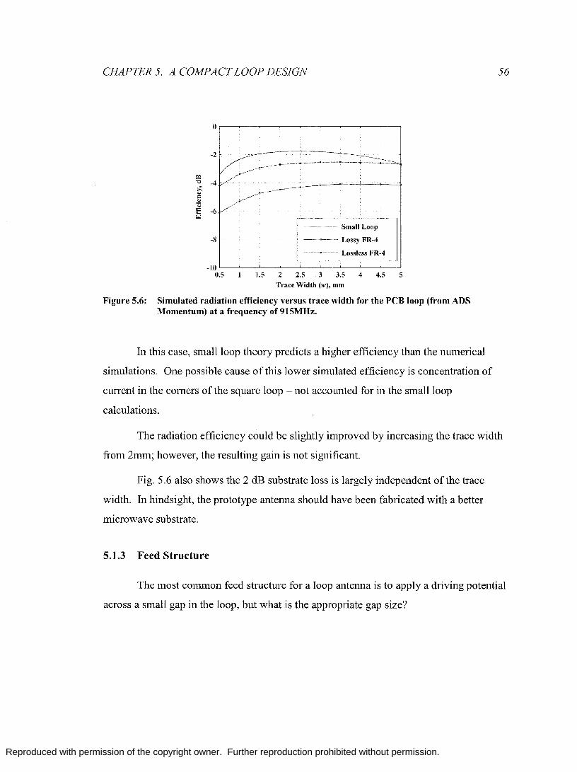
Reproduced with permission of the copyright owner. Further reproduction prohibited without permission.
CHAPTER 5. A COMPACT LOOP DESIGN
-2
-8
------- Small Loop
Lossy FR-4
----------~---------- Lossless _FR-4
-10 L----'-_-'-_..L---'_--'-_--'--_L----'-_-'
0.5 1.5 2 2.5 3 3.5 4 4.5 5 Trace Width (w), mm
Figure 5.6: Simulated radiation efficiency versus trace width for the PCB loop (from ADS Momentum) at a frequency of 915MHz.
In this case, small loop theory predicts a higher efficiency than the numerical
simulations. One possible cause ofthis lower simulated efficiency is concentration of
current in the comers of the square loop - not accounted for in the small loop
calculations.
56
The radiation efficiency could be slightly improved by increasing the trace width
from 2mm; however, the resulting gain is not significant.
Fig. 5.6 also shows the 2 dB substrate loss is largely independent of the trace
width. In hindsight, the prototype antenna should have been fabricated with a better
microwave substrate.
5.1.3 Feed Structure
The most common feed structure for a loop antenna is to apply a driving potential
across a small gap in the loop, but what is the appropriate gap size?
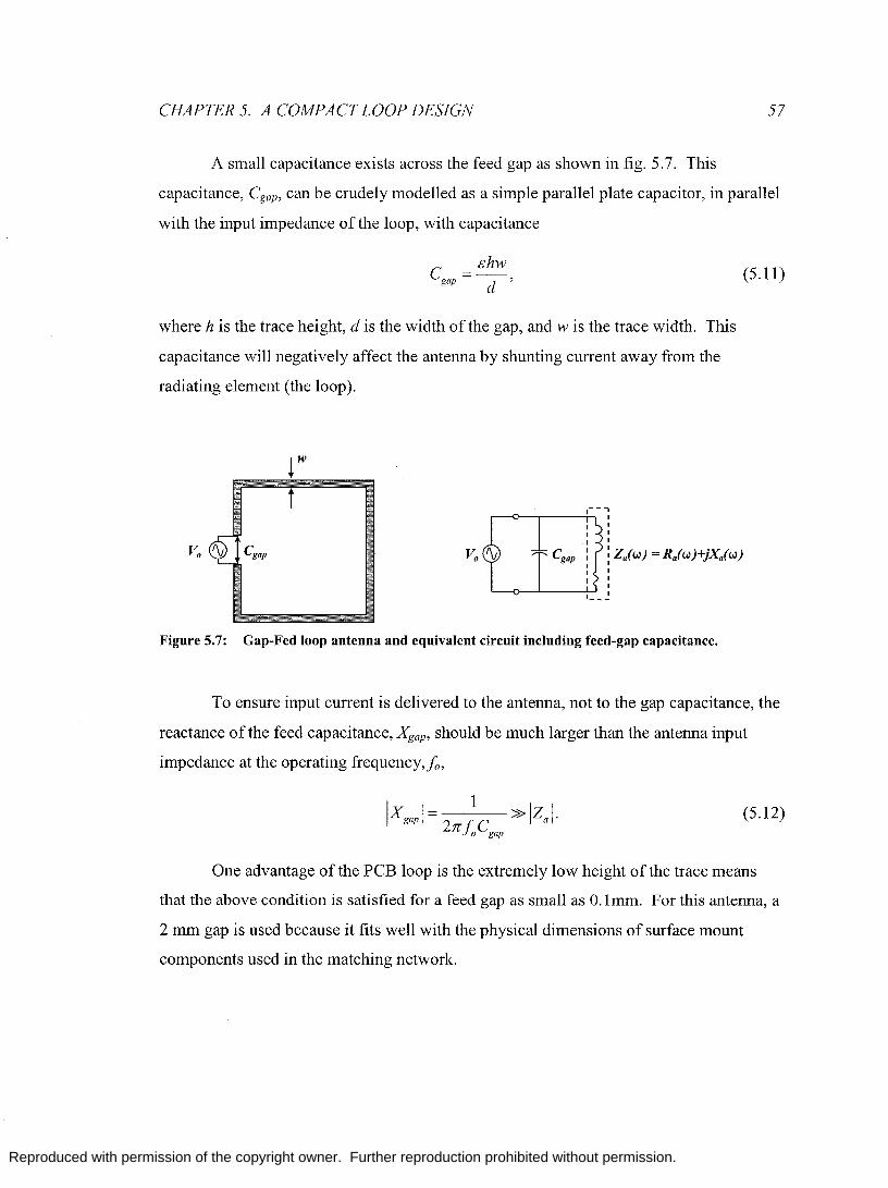
Reproduced with permission of the copyright owner. Further reproduction prohibited without permission.
CHAPTER 5. A COMPACT LOOP DESIGN 57
A small capacitance exists across the feed gap as shown in fig. 5.7. This
capacitance, Cgap, can be crudely modelled as a simple parallel plate capacitor, in parallel
with the input impedance of the loop, with capacitance
&hw Cgap =d'
where h is the trace height, d is the width of the gap, and w is the trace width. This
capacitance will negatively affect the antenna by shunting current away from the
radiating element (the loop).
i r---o---.---_;-,I-- ~
I I I
: Za(w) = Ra(w)+jXa(w) I
Figure 5.7: Gap-Fed loop antenna and equivalent circuit including feed-gap capacitance.
(5.11)
To ensure input current is delivered to the antenna, not to the gap capacitance, the
reactance of the feed capacitance, Xgap , should be much larger than the antenna input
impedance at the operating frequency,la,
I I 1
X = »Z . gap 2;rj
oC
gap 1 al (5.12)
One advantage of the PCB loop is the extremely low height of the trace means
that the above condition is satisfied for a feed gap as small as O.Imm. For this antenna, a
2 mm gap is used because it fits well with the physical dimensions of surface mount
components used in the matching network.

Reproduced with permission of the copyright owner. Further reproduction prohibited without permission.
CHAPTER 5. A COMPACT LOOP DESIGN
Finally, the loop is a symmetrically balanced antenna, and a differential voltage
should be applied to maintain balanced operation.
5.1.4 Coupling with Ground Plane
58
At 915 MHz, the thickness of the ground plane is larger than the skin-depth of
copper (5.1) by a factor of 10. Consequently, RF surface currents are induced on the
ground plane, and these currents re-direct the magnetic near-field around the ground
plane. This causes the ground plane to act as a reflector, distorting the radiation pattern.
Additionally, the ground plane is used as a reference plane by the RF, analog, and digital
electronics, so these RF currents are potentially detrimental and should be minimized.
This coupling can be reduced by increasing the distance between the ground plane
and the loop; however, this can only be done by reducing the size of the loop, and in tum,
the radiation efficiency of the antenna.
The tag antenna was initially simulated without the ground plane using CST, and
the simulated impedance of3.6 + j420 ohms used as a benchmark. The input impedance
with the ground plane gap (distance between the loop conductor and ground plane edge)
of2 mm, previously given as 5.0 + j459.4 ohms is less than ten percent different, so the
gap of 2 mm was deemed adequate.
Fig. 5.8 shows the simulated surface currents on both the ground plane and the
loop. The peak surface-current on the ground plane is on the edge closest to the loop.
The current density in this location is approximately ten percent of the peak current on
the loop, and is 180 degrees out of phase with the current on the closest side ofthe loop,
as is necessary to ensure the high decay of electromagnetic field components within the
ground plane conductor.
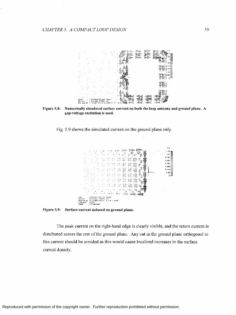
Reproduced with permission of the copyright owner. Further reproduction prohibited without permission.
CHAPTER 5. A COMPACT LOOP DESIGN 59
Type .. Surface Cur.ent (peak) "' MO,nJtor = h-f~el~ ((=91,5) {lJ , <
Maxi .. u .. -3d .13.887 I'll .. at 0.732051 12 I 0.02
Figure 5.8: Numerically simulated surface current on both the loop antenna and ground plane. A gap-voltage excitation is used.
Fig. 5.9 shows the simulated current on the ground plane only.
Type .. Surface Current (peak) Monitor ., h-field ((=915) (1)
MaximulII-3d = 1.13096 AIm at -3 18 / -0.83 frequency .91S Phase .. I:) desrees
Figure 5.9: Surface current induced on ground plane.
L.
AI.
0.721
0.1-97
0.331
9.209
0.05
The peak current on the right-hand edge is clearly visible, and the return current is
distributed across the rest of the ground plane. Any cut in the ground plane orthogonal to
this current should be avoided as this would cause localized increases in the surface
current density.
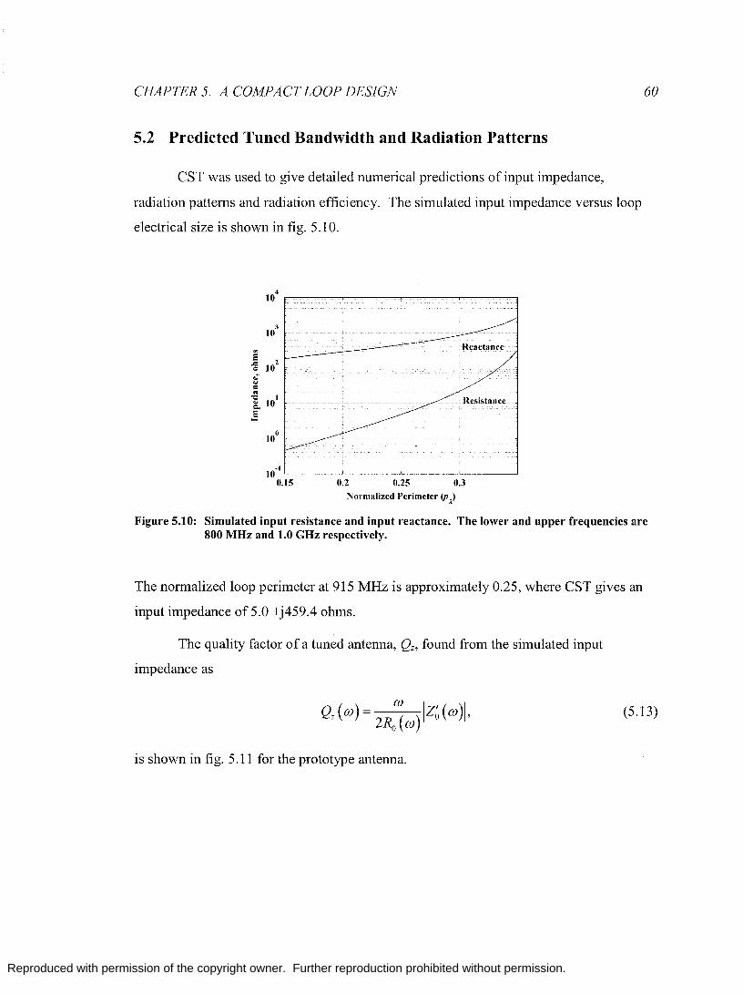
Reproduced with permission of the copyright owner. Further reproduction prohibited without permission.
CHAPTER 5. A COMPACT LOOP DESIGN
5.2 Predicted Tuned Bandwidth and Radiation Patterns
CST was used to give detailed numerical predictions of input impedance,
radiation patterns and radiation efficiency. The simulated input impedance versus loop
electrical size is shown in fig. 5.10.
104
103
8 10
2 .c '" " '"' = '" ""0 1 15. 10 Resistance
e ,....
10°
10 -1
0.15 0.2 0.25 0.3
Normalized Perimeter (p}
60
Figure 5.10: Simulated input resistance and input reactance. The lower and upper frequencies are 800 MHz and 1.0 GHz respectively.
The normalized loop perimeter at 915 MHz is approximately 0.25, where CST gives an
input impedance of 5.0 +j459.4 ohms.
The quality factor of a tuned antenna, Qz, found from the simulated input
impedance as
is shown in fig. 5.11 for the prototype antenna.
(5.13)
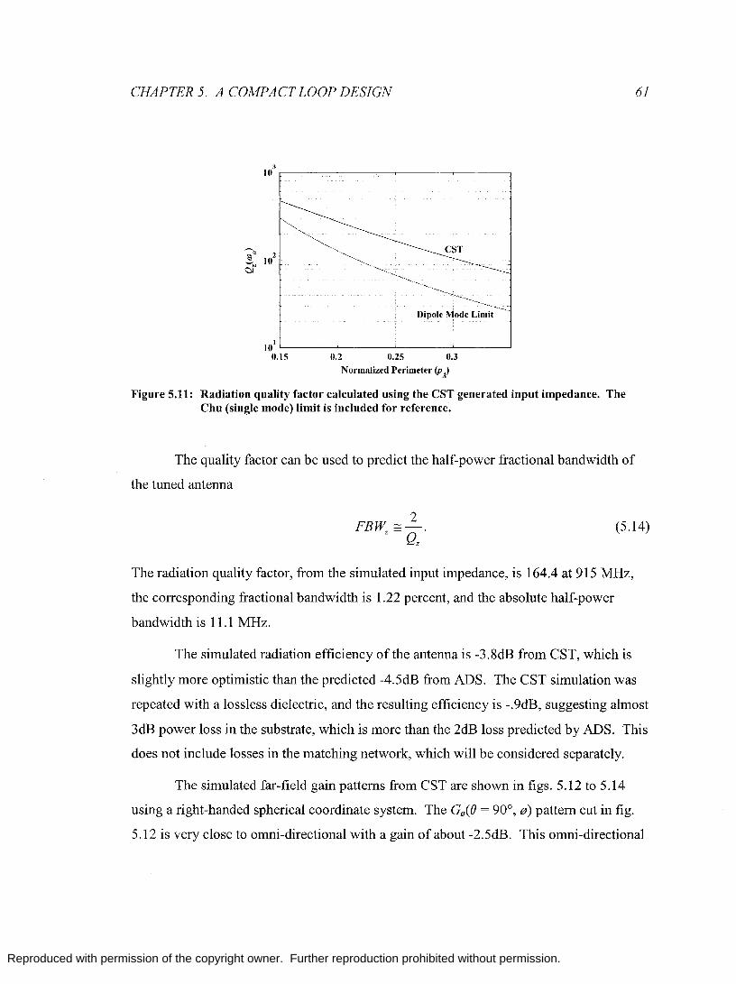
Reproduced with permission of the copyright owner. Further reproduction prohibited without permission.
CHAPTER 5. A COMPACT LOOP DESIGN
~: ,,' ··'-··'·~,"-. •..•••• " ••••.•••. ~CST -..............•.....
Dipole Mode Limit--------
101L-----~------~------~----~ 0.15 0.2 0.25 0.3
Normalized Perimeter (p;)
Figure 5.11: Radiation quality factor calculated using the CST generated input impedance. The Chu (single mode) limit is included for reference.
The quality factor can be used to predict the half-power fractional bandwidth of
the tuned antenna
61
2 FBW ~-.
Z Qz (5.14)
The radiation quality factor, from the simulated input impedance, is 164.4 at 915 MHz,
the corresponding fractional bandwidth is 1.22 percent, and the absolute half-power
bandwidth is 11.1 MHz.
The simulated radiation efficiency of the antenna is -3.8dB from CST, which is
slightly more optimistic than the predicted -4.5dB from ADS. The CST simulation was
repeated with a lossless dielectric, and the resulting efficiency is -.9dB, suggesting almost
3dB power loss in the substrate, which is more than the 2dB loss predicted by ADS. This
does not include losses in the matching network, which will be considered separately.
The simulated far-field gain patterns from CST are shown in figs. 5.12 to 5.14
using a right-handed spherical coordinate system. The GeCO = 90°, g) pattern cut in fig.
5.12 is very close to omni-directional with a gain of about -2.5dB. This omni-directional

Reproduced with permission of the copyright owner. Further reproduction prohibited without permission.
CHAPTER 5. A COMPACT LOOP DESIGN 62
pattern confirms that the coupling with the ground plane is not significant enough to alter
the radiation pattern of the antenna. Only the phi, fJ, polarization is shown because the
theta, fJ, component is negligibly small.
90°
B
0°
_90 0
Figure 5.12: CST simulated far-field pattern Ge«() = 90°, 0) for prototype antenna.
Fig. 5.13 shows both linear polarization components: Go(fJ, fJ = 90°) and
Go(fJ, fJ = 90°). The phi polarization component shows the familiar torroidal shape of the
magnetic dipole (electrically small loop ), and the theta polarization component has a lobe
of close to -10dB on top and bottom of the loop. The electrical size of the loop, close to
one-third of a wavelength, is the cause of this additional lobe, which becomes more
pronounced with increasing loop electrical size.
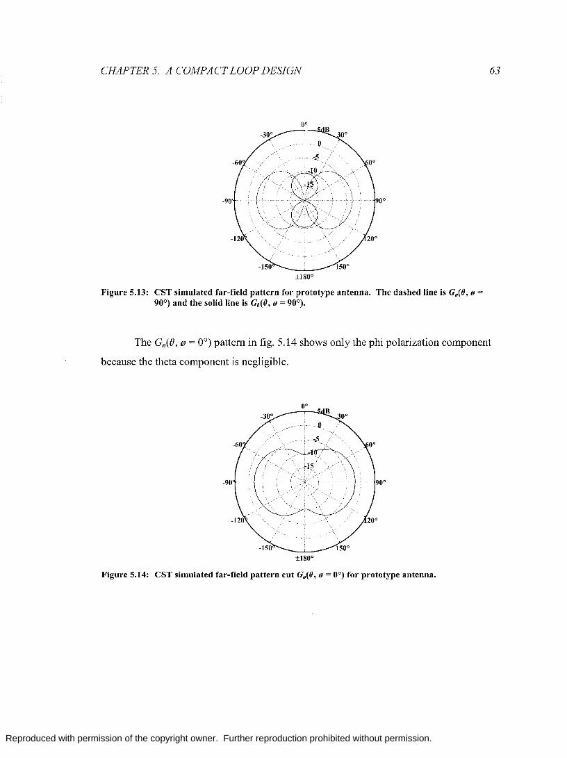
Reproduced with permission of the copyright owner. Further reproduction prohibited without permission.
CHAPTER 5. A COMPACT LOOP DESIGN
Figure 5.13: CST simulated far-field pattern for prototype antenna. The dashed line is Go(8, 0 =
90°) and the solid line is Go(8, 0 = 90°).
63
The Go(8, RJ = 0°) pattern in fig. 5.14 shows only the phi polarization component
because the theta component is negligible.
Figure 5.14: CST simulated far-field pattern cut Go(O, 0 = 0°) for prototype antenna.

Reproduced with permission of the copyright owner. Further reproduction prohibited without permission.
CHAPTER 5. A COMPACT LOOP DESIGN 64
The gain in the horizontal plane, approximately -2.5 dB, is similar to the previous
patterns, and the -10 dB gain in the vertical plane is similar to the gain in the vertical
plane of fig. 5.13.
5.3 Matching Network Design
The matching network topology used to match the differential (balanced) antenna
impedance to a single-ended (unbalanced) fifty ohm microstrip transmission line is
shown in fig. 5.15.
Ziiwo) = 50", single-ended
1:4 Balun
Discrete Matching Za(WO) = (5.0 + j459.4)" Network
r I Zin(WO) = 200", differential
Zin(WO) = (5.0 - j459.4)", differential
Figure 5.15: Differential to single-ended matching network.
A discrete balun4 provides the unbalanced to balanced transformation, and also
provides an impedance transform ratio of 1:4 (unbalanced 50-ohm impedance and
balanced 200 ohm impedance). A balun with a 1: 1 impedance transform ratio would be
better suited for this application, but the 1:4 baluns were the parts on hand at the time of
the design. The design of the discrete matching follows the procedure outlined in section
3.4: the single-ended equivalent is derived first and then converted to a differential
scheme.
4 Johanson Technology part number 0900BL18B200.
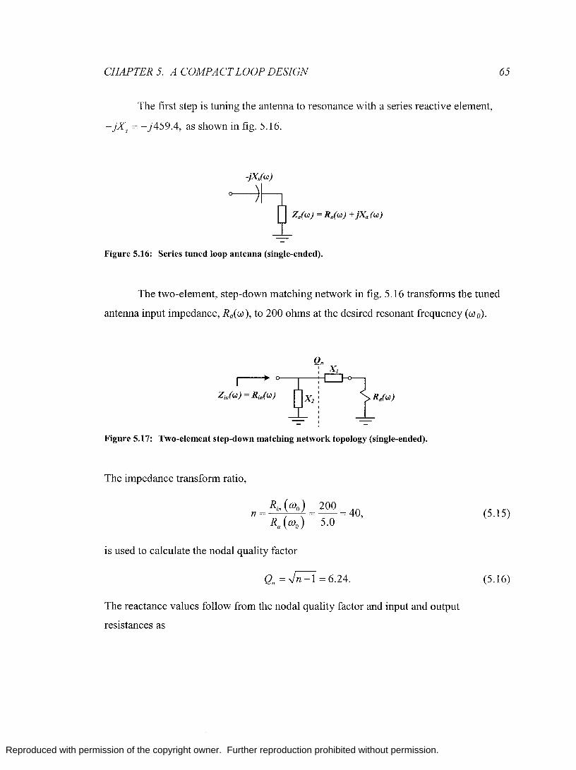
Reproduced with permission of the copyright owner. Further reproduction prohibited without permission.
CHAPTER 5. A COMPACT LOOP DESIGN 65
The first step is tuning the antenna to resonance with a series reactive element,
-jXs =-j459.4, as shown in fig. 5.16.
Figure 5.16: Series tuned loop antenna (single-ended).
The two-element, step-down matching network in fig. 5.16 transforms the tuned
antenna input impedance, Ra( 6J), to 200 ohms at the desired resonant frequency (6J 0).
Figure 5.17: Two-element step-down matching network topology (single-ended).
The impedance transform ratio,
is used to calculate the nodal quality factor
Qn =~ =6.24.
The reactance values follow from the nodal quality factor and input and output
resistances as
(5.15)
(5.16)

Reproduced with permission of the copyright owner. Further reproduction prohibited without permission.
CHAPTER 5. A COMPACT LOOP DESIGN 66
(5.17)
and
(5.18)
The polarity of the reactance XI is chosen to be inductive and the polarity of reactance X2
chosen to be capacitive.
The reactance Xl is in series with the tuning reactance Xs. These two elements
can be combined to yield an equivalent series element
Xeq = j31.2 - j459.4 = - j428.2, (5.19)
reducing the number of elements and ohmic losses.
The resulting single-ended discrete matching network is shown in fig. 5.18.
Figure 5.18: Single-ended discrete matching network.
This network is easily converted to a differential scheme by re-distributing the
series reactance, Xeq, into two equivalent series elements on either side of the antenna as
shown in fig. 5.19.
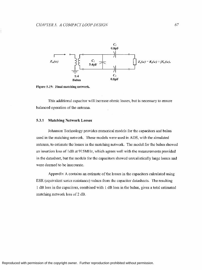
Reproduced with permission of the copyright owner. Further reproduction prohibited without permission.
CHAPTER 5. A COMPACT LOOP DESIGN
Zin(W) 1 C2
5.4pF
--1:4
Balun
Figure 5.19: Final matching network.
c] O.8pF
c3
O.8pF
This additional capacitor will increase ohmic losses, but is necessary to ensure
balanced operation of the antenna.
5.3.1 Matching Network Losses
67
Johanson Technology provides numerical models for the capacitors and balun
used in the matching network. These models were used in ADS, with the simulated
antenna, to estimate the losses in the matching network. The model for the balun showed
an insertion loss of IdB at 915MHz, which agrees well with the measurements provided
in the datasheet, but the models for the capacitors showed unrealistically large losses and
were deemed to be inaccurate.
Appendix A contains an estimate of the losses in the capacitors calculated using
ESR (equivalent series resistance) values from the capacitor datasheets. The resulting
1 dB loss in the capacitors, combined with 1 dB loss in the balun, gives a total estimated
matching network loss of 2 dB.

Reproduced with permission of the copyright owner. Further reproduction prohibited without permission.
CHAPTER 5. A COMPACT LOOP DESIGN 68
5.4 Measurements
The surface mount balun and discrete matching network allows measurement of
the antenna input impedance with a VNA. A one-port calibration sequence using discrete
surface mount components as calibration standards shifts the reference plane of the
network analyzer as shown in fig. 5.21. This shifted reference plane allows direct
measurement of the antenna impedance. This calibration technique characterises the
balun as a systematic measurement error and removes it from the measurement along
with the other systematic errors.
50° micros trip
SMA connector toVNA
1:4 Balun
Reference Plane
Figure 5.20: VNA measurement of antenna input impedance.
The prototype antenna includes footprints for additional series matching elements
labelled RJ and R2 . These are not needed and are populated with zero-ohm resistors.
A one-port calibration sequence requires three calibration standards: an open, a
50-ohm load, and a short. During the calibration process the footprint for C2 is used for
calibration standards, and C2 and C3 must be left open (unpopulated). A surface mount
fifty ohm resistor is used as the fifty ohm load standard, a zero-ohm resistor as the short
standard, and the pad is left unpopulated for the open standard.

Reproduced with permission of the copyright owner. Further reproduction prohibited without permission.
CHAPTER 5. A COMPACT LOOP DESIGN 69
Calibration standards include definitions that mathematically model the electrical
characteristics of each standard. These definitions account for imperfections such as
open circuit fringing capacitance and parasitic series inductance in the short standard.
Surface mount components are far less ideal than proper calibration standards, so the
resulting measurement accuracy is reduced; however, at the relatively low operating
frequency of 915 MHz, surface mount components will still yield useful measurement
data.
After calibration is complete, populating C2 and C3 with zero-ohm resistors and
leaving the C 1 footprint open allows direct measurement of the antenna impedance. The
series impedance of the zero-ohm resistors is included in the measurement, but should not
produce significant errors at 915 MHz.
There are additional limitations with this measurement technique. The antenna is
not matched to the 50-ohm impedance of the measurement set-up, so the return loss is
extremely high and very little power propagates through the balun to the antenna. The
signal to noise ratio (SNR) of the measurement is very low, compounded by noise
generated from the antenna itself. It is crucial to use the maximum available power and
the noise reduction features (low IF bandwidth and time averaging) of the VNA to
maximise the SNR of the measurement.
The measured antenna input impedance is shown in fig. 5.22 with the simulated
input impedance from CST. The high noise of the measurement is visible in the
measurement of input resistance. Although noisy, the measured impedance is clearly
similar to the simulated impedance. There is a distinctive dip in the measured resistance
at normalized perimeter of 0.25. This phenomenon was present in repeated
measurements, and although this is the desired resonant frequency of the antenna, this
measurement of the loop does not contain any tuning specific to this frequency. This
irregularity is likely caused by the balun or the surface mount components used as
calibration standards.

Reproduced with permission of the copyright owner. Further reproduction prohibited without permission.
CHAPTER 5. A COMPACT LOOP DESIGN 70
The simulated impedance diverges from the measured impedance at the upper end
of the measurement, showing that the first anti-resonance of the simulated loop occurs at
a slightly lower frequency than the measured loop.
104 ~====~====~~------~------1 I == ~~;sured I
oS <.J
= '"
103 L L. __________ -,-J.
"0 I ~ 10 S ...
Reactance
0.25 0.3 Normalized Perimeter (p)
Figure 5.21: Measured loop input impedance and simulated CST input impedance.
This measurement approach is also useful for testing and tuning the matching
network. By sequentially populating various components of the matching network,
starting with C] and C3, the nodal input impedances can be directly measured and
compared with the expected nodal impedances.
Figs. 5.23 and 5.24 show the measured nodal impedances of the matching
network. These measurements were taken after the component values had been manually
tuned, so the component values are slightly different than theoretically calculated values.
Fig 5.23 shows the measured nodal impedance of the antenna plus the series
elements. The measured impedance of 6 + j27 ohms is reasonably close to the expected
impedance of 5 + j31.2 ohms.
Fig 5.24 shows the measured nodal impedance with both the series and shunt
elements populated. The measured impedance of 166 + j5.3 is smaller than the expected
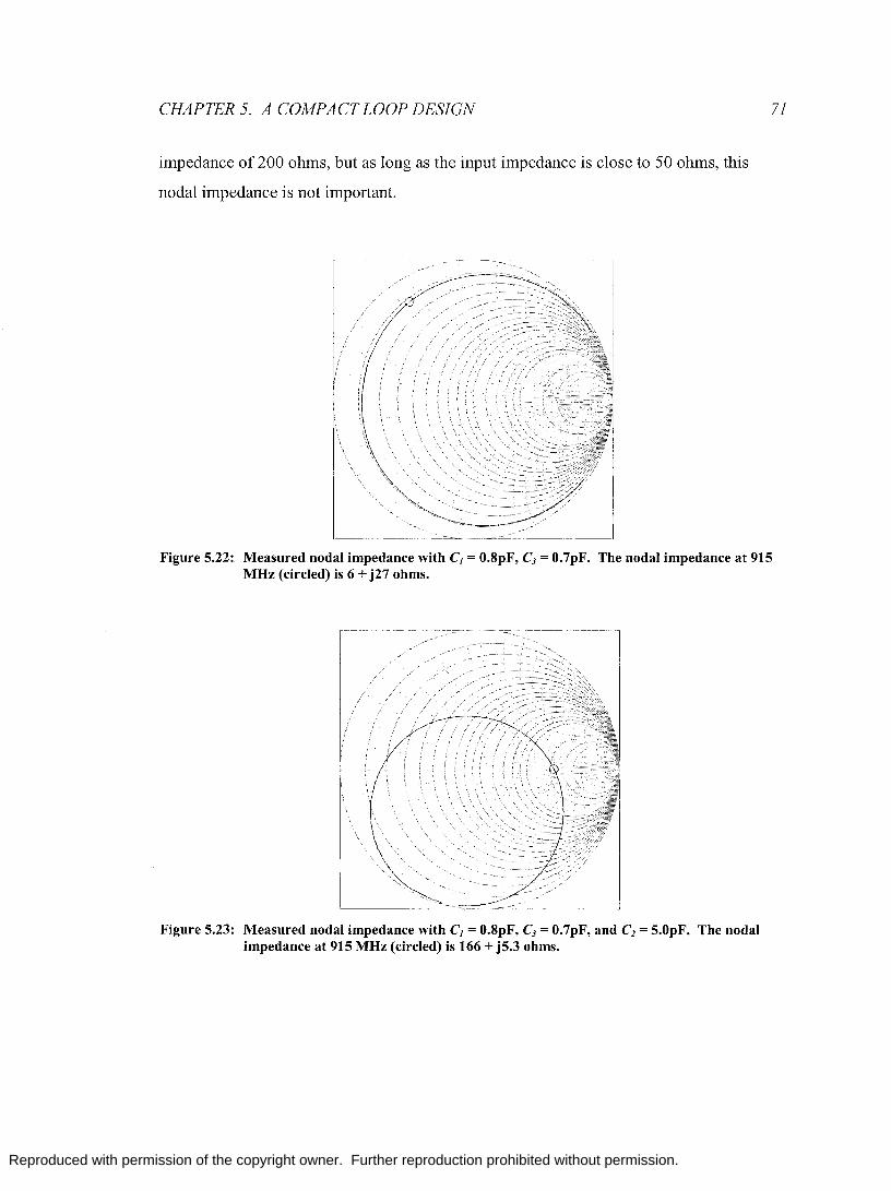
Reproduced with permission of the copyright owner. Further reproduction prohibited without permission.
CHAPTER 5. A COMPACT LOOP DESIGN
impedance of 200 ohms, but as long as the input impedance is close to 50 ohms, this
nodal impedance is not important.
71
Figure 5.22: Measured nodal impedance with C] = O.8pF, C3 = O.7pF. The nodal impedance at 915 MHz (circled) is 6 + j27 ohms.
Figure 5.23: Measured nodal impedance with C] = O.8pF, C3 = O.7pF, and C] = 5.0pF. The nodal impedance at 915 MHz (circled) is 166 + j5.3 ohms.
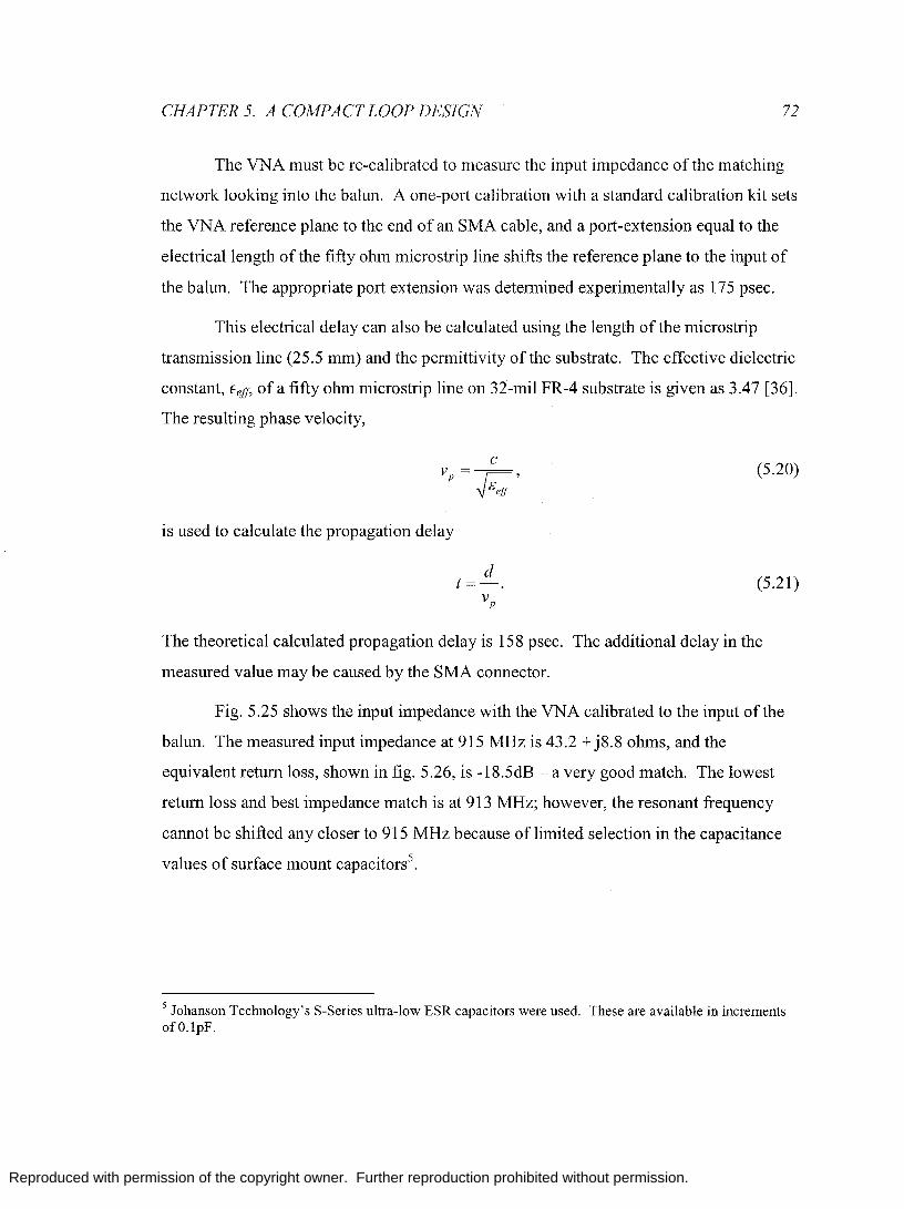
Reproduced with permission of the copyright owner. Further reproduction prohibited without permission.
CHAPTER 5. A COMPACT LOOP DESIGN 72
The VNA must be re-calibrated to measure the input impedance of the matching
network looking into the balun. A one-port calibration with a standard calibration kit sets
the VNA reference plane to the end of an SMA cable, and a port-extension equal to the
electrical length of the fifty ohm microstrip line shifts the reference plane to the input of
the balun. The appropriate port extension was determined experimentally as 175 psec.
This electrical delay can also be calculated using the length of the microstrip
transmission line (25.5 mm) and the permittivity of the substrate. The effective dielectric
constant, EejJ, of a fifty ohm microstrip line on 32-mil FR-4 substrate is given as 3.47 [36].
The resulting phase velocity,
(5.20)
is used to calculate the propagation delay
d t=-. (5.21)
vp
The theoretical calculated propagation delay is 158 psec. The additional delay in the
measured value may be caused by the SMA connector.
Fig. 5.25 shows the input impedance with the VNA calibrated to the input of the
balun. The measured input impedance at 915 MHz is 43.2 + j8.8 ohms, and the
equivalent return loss, shown in fig. 5.26, is -18.5dB - a very good match. The lowest
return loss and best impedance match is at 913 MHz; however, the resonant frequency
cannot be shifted any closer to 915 MHz because oflimited selection in the capacitance
values of surface mount capacitors5.
5 Johanson Technology's S-Series ultra-low ESR capacitors were used. These are available in increments ofO.lpF.
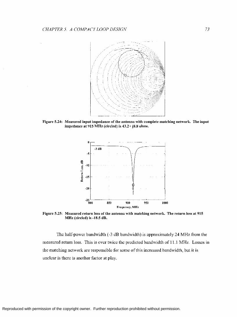
Reproduced with permission of the copyright owner. Further reproduction prohibited without permission.
CHAPTER 5. A COMPACT LOOP DESIGN 73
Figure 5.24: Measured input impedance of the antenna with complete matching network. The input impedance at 915 MHz (circled) is 43.2+ j8.8 ohms.
0
-5
= "0 ~ -10 0 .... = .. .E -15 '" c:=:
-20
-25 800
-3 dB
850 900 Frequency, MHz
950 1000
Figure 5.25: Measured return loss of the antenna with matching network. The return loss at 915 MHz (circled) is -18.5 dB.
The half-power bandwidth (-3 dB bandwidth) is approximately 24 MHz from the
measured return loss. This is over twice the predicted bandwidth of 11.1 MHz. Losses in
the matching network are responsible for some of this increased bandwidth, but it is
unclear is there is another factor at play.
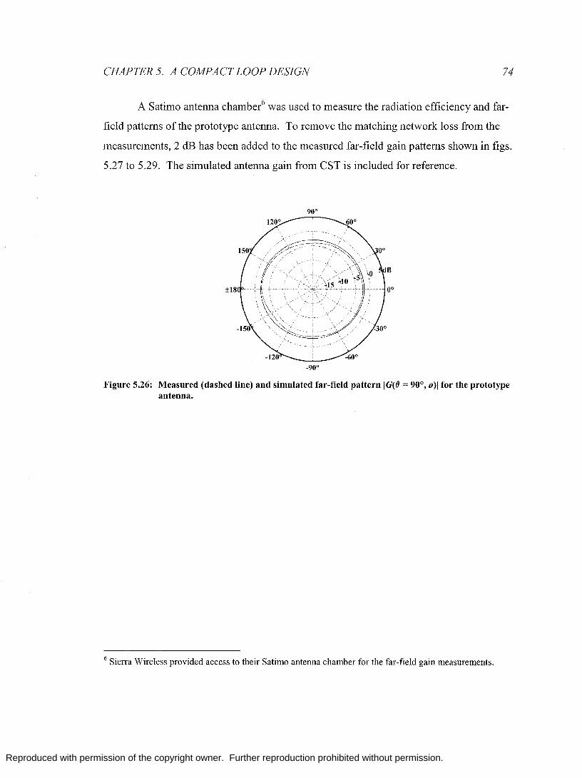
Reproduced with permission of the copyright owner. Further reproduction prohibited without permission.
CHAPTER 5. A COMPACT LOOP DESIGN 74
A Satimo antenna chamber6 was used to measure the radiation efficiency and far
field patterns of the prototype antenna. To remove the matching network loss from the
measurements, 2 dB has been added to the measured far-field gain patterns shown in figs.
5.27 to 5.29. The simulated antenna gain from CST is included for reference.
900
_90 0
Figure 5.26: Measured (dashed line) and simulated far-field pattern IG(8 = 90°, 0)1 for the prototype antenna.
6 Sierra Wireless provided access to their Satimo antenna chamber for the far-field gain measurements.

Reproduced with permission of the copyright owner. Further reproduction prohibited without permission.
CHAPTER 5. A COMPACT LOOP DESIGN 75
_30° 0°
__ ~---':wB 300
o
±I 80°
Figure 5.27: Measured (dashed line) and simulated (solid line) far-field pattern IG(O, 0 = 90°)1 for the prototype antenna.
±I80°
Figure 5.28: Measured (dashed line) and simulated (solid line) far-field pattern IG(O, 0 = 0°)1 for prototype antenna.
The measured radiation efficiency of the antenna and the matching network was
-6.6 dB. The simulated radiation efficiency (-3.8 dB radiation efficiency) and matching
loss (2 dB matching loss) was estimated as -5.8dB, so the error between the predicted and
measured efficiency is less than 1 dB.
Reproduced with permission of the copyright owner. Further reproduction prohibited without permission.
Chapter 6
Conclusions
The loop antenna can be an effective compact planar antenna, especially suited
for applications in small wireless tags, and unlike many other low-profile or planar
antennas, the loop antenna does not need a ground plane.
Chapter 2 reviewed previously derived solutions for the current distribution and
input impedance of the electrically large thin-wire loop, and used these results to derive
the theoretical radiation efficiency, not previously available, and half-power bandwidth of
the tuned loop antenna. Fig. 6.1 shows the derived radiation efficiency and tuned
bandwidth for a circular thin-wire loop antenna. This figure concisely summarizes the
important results from this analysis: both the bandwidth and radiation efficiency improve
with increasing electrical size, and a loop with normalized perimeter greater than one-half
is a very efficient radiator.
A sharp anti-resonance at an electrical perimeter of approximately one-half makes
impedance matching at this size exceedingly difficult, and operation in the area should be
avoided. It is suggested that the optimum loop electrical size, depending on the
bandwidth requirements of the system, is a normalized perimeter between one-half and
one. It is possible that bandwidth demands require a further increase in electrical size,
but from a radiation efficiency point of view, there is little point in using a larger loop.
76
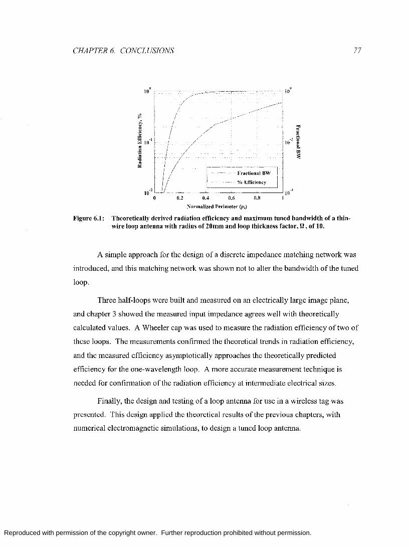
Reproduced with permission of the copyright owner. Further reproduction prohibited without permission.
CHAPTER 6. CONCLUSIONS
~-- Fractional BW
----- % Efficiency
o 0.2 0.4 0.6 0.8
Normalized Perimeter (PA)
Figure 6.1: Theoretically derived radiation efficiency and maximum tuned bandwidth of a thinwire loop antenna with radius of 20mm and loop thickness factor, n, of 10.
77
A simple approach for the design of a discrete impedance matching network was
introduced, and this matching network was shown not to alter the bandwidth of the tuned
loop.
Three half-loops were built and measured on an electrically large image plane,
and chapter 3 showed the measured input impedance agrees well with theoretically
calculated values. A Wheeler cap was used to measure the radiation efficiency of two of
these loops. The measurements confirmed the theoretical trends in radiation efficiency,
and the measured efficiency asymptotically approaches the theoretically predicted
efficiency for the one-wavelength loop. A more accurate measurement technique is
needed for confirmation of the radiation efficiency at intermediate electrical sizes.
Finally, the design and testing of a loop antenna for use in a wireless tag was
presented. This design applied the theoretical results of the previous chapters, with
numerical electromagnetic simulations, to design a tuned loop antenna.

Reproduced with permission of the copyright owner. Further reproduction prohibited without permission.
Appendix A
Matching Network Loss Calculations
This appendix estimates the ohmic loss in the capacitors in this matching network
shown in fig. A.I. Losses in the balun are considered separately. It should be
emphasized that many simplifications are used in this analysis, and the resulting loss
should be treated as a rough estimate. The carrier frequency is 9I5MHz, and the transmit
power is 4dBm, or 2.5m W.
1:4 Balun
C2
5.4pF
Figure A.l: Prototype antenna matching network.
C1
O.8pF
C3
O.8pF
First, the balun is replaced with an ideal voltage source delivering 2.5m W of
power into a resistive load of 200 ohms,
78
(A.I)
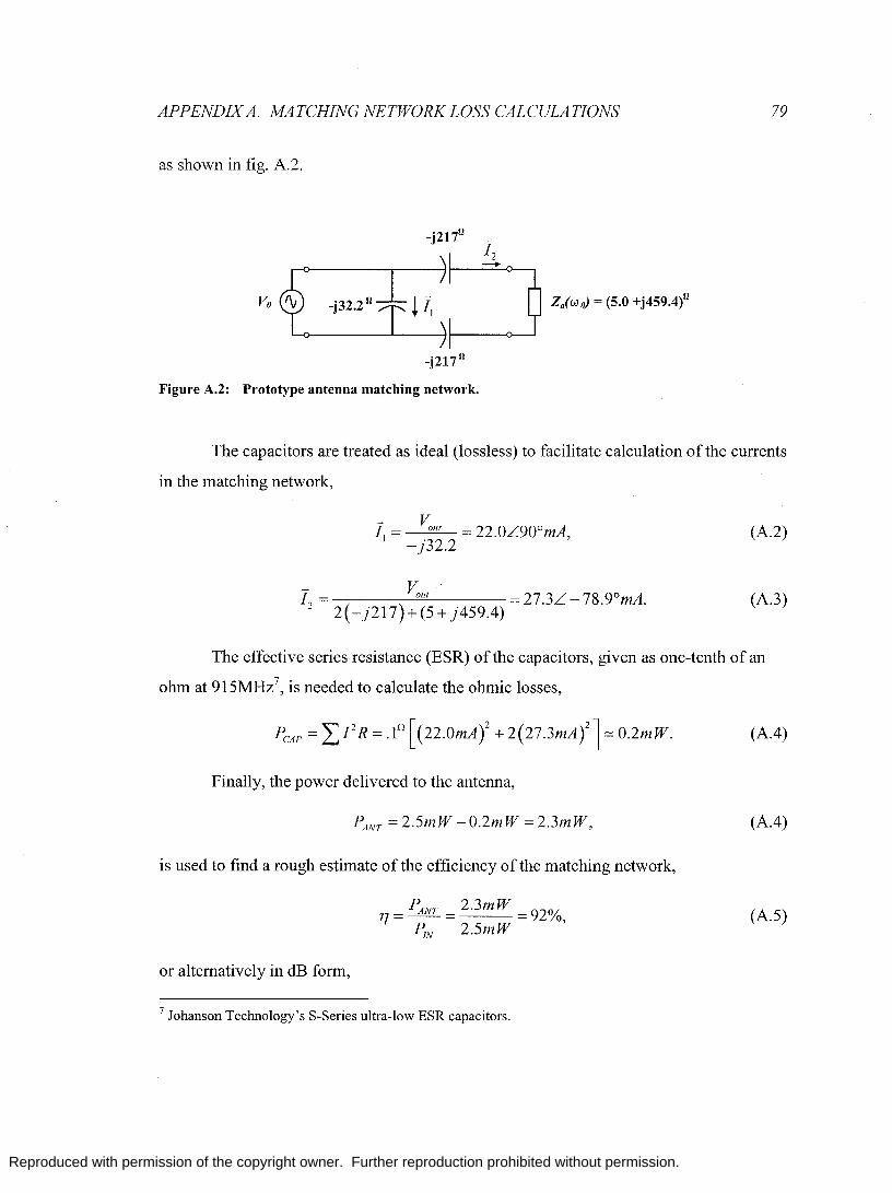
Reproduced with permission of the copyright owner. Further reproduction prohibited without permission.
APPENDIX A. MATCHING NETWORK LOSS CALCULATIONS 79
as shown in fig. A.2.
-j32.2 fI
Figure A.2: Prototype antenna matching network.
The capacitors are treated as ideal (lossless) to facilitate calculation of the currents
in the matching network,
1 = ~ut = 22.0L90omA I _ j32.2 '
(A.2)
12 = ~lIt = 27.3L-78.9°mA. 2(-j217)+(5+ j459.4)
(A.3)
The effective series resistance (ESR) of the capacitors, given as one-tenth of an
ohm at 915MHz7, is needed to calculate the ohmic losses,
(A. 4)
Finally, the power delivered to the antenna,
P'4NT = 2.5mW -O.2mW = 2.3mW, (AA)
is used to find a rough estimate of the efficiency of the matching network,
_ PANT _ 2.3mW _ 9201 l] - - - 10,
~N 2.5mW (A.5)
or alternatively in dB form,
7 Johanson Technology's S-Series ultra-low ESR capacitors.
Reproduced with permission of the copyright owner. Further reproduction prohibited without permission.
APPENDIX A. MATCHING NETWORK LOSS CALCULATIONS 80
lJdB =10log(lJ)=-AdB. (A.6)
This estimate should be rounded down to at least -1 dB to provide some margin of
error, given the approximate nature of the calculation.

Reproduced with permission of the copyright owner. Further reproduction prohibited without permission.
Bibliography
[1] H. C. Pocklington, "Electrical oscillations in wires," Proc. Cambridge Phys.
SOc., vol. 9, pp. 324-333, 1897.
[2] J. D. Kraus, R. J. Marhefka, Antennas for All Applications. Third Edition,
McGraw Hill, New York, 2002.
[3] W.L. Stutzman, G.A Thiele, Antenna Theory and Design. John Wiley and
Sons, New York, 1981.
[4] AB. Balanis, Antenna Theory, Analysis and Design. Third Edition, John Wiley
and Sons, New York, 2005.
[5] S. Ramo, J. R. Whinnery, T. Van Duzer, Fields and Waves in Communications
Electronics. John Wiley and Sons, New York, 1965.
[6] E. Hallen, "Theoretical investigation into transmitting and receiving qualities of
antennae," Nova Acta Regiae SOc. Ser. Upps., vol. II, pp. 1 4, Nov. 4,1938.
[7] J. E. Storer, "Impedence of thin-wire loop antennas," Trans. AlEE, vol. 75, pp.
606-619, Nov. 1956.
[8] P. A Kennedy, "Loop antenna measurements," IEEE Trans. Antennas
Propagat., vol. AP-4, pp. 610-618, Oct. 1956.
[9] T. T. Wu, "Theory of the Thin Circular Loop Antemla," Journal of
Mathematical Physics, vol. 3, pp. 1301-1304, Nov. - Dec. 1962.
81
Reproduced with permission of the copyright owner. Further reproduction prohibited without permission.
BIBLIOGRAPHY
[10] C.-L. Chen, R. W. P. King, "The small bare loop antenna immersed in a
dissipative medium," IEEE Trans. Antennas Propagat., vol. AP-l1, pp. 266-
269, May 1963.
[11] R. W. P. King, C. W. Harrison Jr., D. G. Tingley, "The admittance of bare
circular loop antennas in a dissipative medium," IEEE Trans. Antennas
Propagat., vol. AP-12, pp. 434-438, July 1964.
82
[12] R. W. P. King, C. W. Harrison Jr., D. G. Tingley, "The current in bare circular
loop antennas in a dissipative medium," IEEE Trans. Antennas Propagat., vol.
AP-13, pp. 529-531, July 1965.
[13] R. W. P. King, Antenna Theory, Part 1. Chapter 11, R. E. Collin and F. J.
Zucker editors, McGraw-Hill, New York, 1969.
[14] G. S. Smith, "A note on the imperfectly conducting circular-loop antenna,"
Radio Science Journal, vol. 8, pp. 711-725, July 1973.
[15] G. S. Smith, "On the electrically small bare loop antenna in a dissipative
medium," IEEE Trans. Antennas Propagat., vol. AP-24, pp. 533-537, July
1976.
[16] R. W. P. King, G. S. Smith, Antennas in Matter: Fundamentals, Theory and
Applications. MIT Press, Cambridge, MA, 1981.
[17] Q. Balzano, K. Siwiak, "The near field of annular antennas," IEEE Trans.
Vehicular Tech., vol. VT-36, pp. 173-183, Nov. 1987.
[18] G. Zhou, G. S. Smith, "An accurate theoretical model for the thin-wire circular
half-loop antenna," IEEE Trans. Antennas Propagat., vol. AP-39, pp. 1167-
1177, Aug. 1991.
[19] lB. Sherman, "Circular loop antennas at ultra-high frequencies," Proc. IRE,
vol. 32, pp. 534-537, Sept. 1944.
Reproduced with permission of the copyright owner. Further reproduction prohibited without permission.
BIBLIOGRAPHY
[20] G. Glinski, "Note on the circular loop antennas with non-uniform current
distribution," J Appl. Phys., vol. 18, pp. 638-644, July 1947.
83
[21] E. J. Martin, Jr., "Radiation fields of circular loop antennas by a direct
integration process," IEEE Trans. Antennas Propagat., vol. AP-8, pp. 105-107,
Jan. 1960.
[22] J. E. Lindsay, Jr., "A circular loop antenna with non-uniform current
distribution," IEEE Trans. Antennas Propagat., vol. AP-8, pp. 439-441, July
1960.
[23] B. R. Rao, "Far-field patterns oflarge circular loop antennas: Theoretical and
experimental results," IEEE Trans. Antennas Propagat., vol. AP-16, pp. 269-
270, Mar. 1968.
[24] D. H. Werner, "An exact integration procedure for vector potentials of thin
circular loop antennas," IEEE Trans. Antennas Propagat., vol. AP-44, pp. 157-
165, Feb. 1996.
[25] L. W. Li, M. S. Leong, P. S. Kooi, T. S. Yeo, "Exact solutions of
electromagnetic fields in both near and far zones radiated by thin circular-loop
antennas: a general representation," IEEE Trans. Antennas Propagat., vol. AP-
45, pp. 1741-1748, Dec. 1997.
[26] L.W. Li, C.P. Lim, and M.S. Leong, "Method-of-moments analysis of
electrically large circular loop antennas: Non-uniform current," Proc. Inst.
Elect. Eng. Microw. Antennas Propag., vol. 146, pp. 416-420, 1999.
[27] L.W. Li, S. Krishnan, M.S. Leong, P. S. Kooi, "Radiation Q of electrically large
loop antennas with non-uniform currents," Microwave and Optical Technology
Letters, vol. 34, pp. 377-380, Sept. 2002.
Reproduced with permission of the copyright owner. Further reproduction prohibited without permission.
BIBLIOGRAPHY
[28] IT. Conway, "New exact solution procedure for the near fields of the general
thin circular loop antenna," IEEE Trans. Antennas Propagat., vol. AP-53, pp.
509-517, Jan. 2005.
[29] AD. Yaghjian, S.R. Best, "Impedance, bandwidth, and Q of antennas," IEEE
Trans. Antennas Propagat., vol. AP-53, pp. 1298-1324, Apr. 2005.
[30] AD. Yaghjian, S.R. Best, "The lower bounds on Q for lossy electric and
magnetic dipole antennas, " IEEE Antennas Wireless Propag. Lett., vol. 3, pp.
314-316,2004.
84
[31] J. S. McLean, "A re-examination of the fundamental limits on the radiation Q of
electrically small antennas," IEEE Trans. Antennas Propagat., vol. AP-44, pp.
672-676, May 1996.
[32] R. C. Hansen, "Fundamental limitations in antennas," Proc. IEEE, vol. 69, pp.
170-182, Feb. 1981.
[33] H. A Wheeler, "Fundmentallimitations of small antennas," Proc. IRE, vol. 35,
pp. 1479-1484, Dec. 1947.
[34] L. J. Chu, "Physical limitations on omni-directional antennas," J Appl. Phys.,
vol. 19, pp. 1163-1175, Dec. 1948.
[35] "Impedance matching networks applied to RF power transistors," Motorola
application note AN721 , 1993.
[36] R. Ludwig, P. Bretchko, RF Circuit Design: Theory and Applications. Prentice
Hall, New Jersey, 2000
[37] G. Gonzales, Microwave Transistor Amplifiers, Analysis and Design. Second
Edition, Prentice Hall, New Jersey, 1997
[38] R. Vaughan, J.B. Andersen, Channels, Propagation and Antennasfor Mobile
Communications. The Institution of Electrical Engineers, London, 2003.

Reproduced with permission of the copyright owner. Further reproduction prohibited without permission.
BIBLIOGRAPHY 85
[39] H. A. Wheeler, "The radiansphere around a small antenna", Proc. IRE, vol. 47,
pp. 1325 ~ 1331, Aug. 1959
[40] E. H. Newman, P. Bohley, and C. H. Walter, "Two methods for the
measurement of antenna efficiency," IEEE Trans. Antennas Propagat., vol. AP-
23, pp. 457-461, July 1975.
[41] D. M. Pozar, B. Kaufman, "Comparison of three methods for the measurement
of printed antenna efficiency," IEEE Trans. Antennas Propagat., vol. 36, pp.
136-139,Jan.1988.
[42] G. S. Smith, "An analysis of the wheeler method for measuring the radiating
efficiency of antennas," IEEE Trans. Antennas Propagat., vol. 25, pp. 552-556,
Jut 1977.
[43] D.K. Cheng, Field and Wave Electronics, Second Edition. Addison Wesley,
New York, 1992.
[44] R. S. Elliot, Electromagnetics. McGraw Hill, New York, 1966.
[45] J. D. Kraus, Electromagnetics. Fourth Edition, McGraw Hill, New York, 1992.
[46] G.S. Smith, An Introduction to Classical Electromagnetic Radiation.
Cambridge University Press, Cambridge, 1997.
[47] Antenna Engineering Handbook. Third Edition, R.c. Johnson, editor, McGraw
Hill, New York, 1993, in particular Ch.5: Loop Antennas, G.S. Smith, and Ch.
6: Small Antennas, H.A. Wheeler.
[48] J.R. Aguilar, M. Beadle, P.T. Thompson, M.W. Shelley, "The microwave and
RF characteristics ofFR4 substrates," lEE Colloquium on Low Cost Antenna
Technology, pp. 2/1-2/6, Feb. 1998.
[49] S. Adachi, Y. Mushiaki, "Theoretical formulation for circular loop antennas by
integral equation method," Sci. Rep. RITU, vol. 9, pp. 9-18, 1957.

Reproduced with permission of the copyright owner. Further reproduction prohibited without permission.
BIBLIOGRAPHY
[50] S. Adachi, Y. Mushiaki, "Studies of large circular loop antennas," Sci. Rep.
RITU, vol. 9, pp. 79-103, 1957.
[51] S. Adachi, Y. Mushiaki, "Directive loop antenna," Sci. Rep. RITU, vol. 9, pp.
105-112, 1957.
[52] T. Kasahara, S. Adachi, and Y. Mushiake, "Calculation of the impedances of
impedance-terminated loop antennas by the EMF method," Electronics and
Communications in Japan (IECE of Japan Trans.), vol. 52, pp 73-80, 1969.
86