Embed Size (px)
Citation preview

Nuclear Instruments and Methods in Physics Research A 376 (1996) 319-334 NUCLEAR
INSTRUMENTS & METNODS IN PHYSICS RESEARCH
Section A
A study on the properties of lead tungstate crystals
R.Y. Zhu a**, D.A. Maa, H.B. Newman”,’ C.L. Woodyb, J.A. Kiersteadb, S.P. Stollb, P.W. Levy b*2
a California Institute of Technology. Pasadena, CA 91125, USA b Brookhaven National Loborarov, Upton, NY 11973, USA
Received 5 February 1996
Abstract This report summarizes the results of a study on the properties of five large and five small size lead hmgstate (PbW04)
crystals. Data are presented on the longitudinal optical transmittance and light attenuation length, light yield and response uniformity, emission spectra and decay time. The radiation resistance of large crystals and possible curing with optical bleaching are discussed. The result of an in depth materials study, including trace impurities analysis, are also presented. The general conclusion from this investigation is that further research and development is needed to develop fast, radiation- hard PbW04 crystals for the CMS experiment at the CERN LHC.
1. Introduction
As one of two future experiments at the Large Hadron Collider (LHC) at CERN, the Compact Muon Solenoid (CMS) collaboration decided to construct a precision elec- tromagnetic calorimeter consisting of 110000 lead tungstate (PbW04) crystals [ 11. This decision followed extensive re- search and development carried out by the physics commu- nity pursuing a precision electromagnetic calorimeter aim- ing at searches for the Higgs boson in the intermediate mass region [ 2-51. Several fast scintillating crystals (BaFz, CeF3, undoped CsI and PbWO4) were thoroughly investi- gated [ 6,7] for this physics motivation. Lead tungstate was chosen by the CMS experiment [ 1 ] because of its high den- sity, low cost and fast decay time.
Lead hmgstate (PbW04) crystals are a new type of heavy scintillator which have a high density of 8.3 gcme3, a short radiation length of 0.89 cm and a small Molibre radius of 2.2 cm. They are known to have a complicated emission spec- ttim and a fast decay time [8-l 11. Measurements also indi- cate that PbWO4 crystals produced by different manufactur- ers have different emission spectra, and some crystals may have significant slow components [ 121. In this report, we present a study on the properties of five large PbW04 crys- tals and a small sample grown by the Czochralski method in
*Corresponding author. Tel. +1 818 3956661, fax +I 818 7953951, e-mail [email protected].
’ Supported in part by U.S. Deparanent of Energy Grant No. DE-FGO3- 92-ER40701.
* Supported in part by U.S. Department of Energy Contract No. DE-ACOZ-
CH7600016.
Bogoroditsk, Russia, along with four small samples grown at Shanghai Institute of Ceramics (SIC) in China. The large Bogoroditsk samples are considered to be full calorimeter size crystals for CMS. Among four SIC small samples, three were grown by the modified Bridgman method, and one by the Czochralski method.
The work presented in this report is part of an ongoing effort aimed at understanding the performance of full size PbW04 crystals at LHC. To realize the superb energy reso- lution promised by a PbWO4 crystal calorimeter in the hos- tile environment at LHC, where a dose of 1 to 10 Mrad of electromagnetic radiation and 10’3-10’4 cm-* of neutron fluence are expected in ten years of operation [ 11, the sta- bility of the light output of PbW04 crystals in situ is a cru- cial issue. The radiation resistance was measured for five full size PbWO4 samples, and it was found that all samples suffer from radiation damage to different degrees. An in- vestigation was also made to study the stoichiometric ratio of Pb : W and impurities in these crystals. Preliminary con- clusions have been drawn on possible causes of the slow scintillation and poor radiation resistance in some samples. The results indicate that further research and development is needed to improve the quality of PbWO4 crystals being produced for the CMS collaboration.
Section 2 describes crystal samples and the experimental apparatus used in this investigation. The result of the mea- surements on crystal properties, such as transmittance, emis- sion spectra, decay times, light yield and light response uni- formity are presented in Section 3. Section 4 discusses the results on crystal radiation damage, possible curing through optical bleaching and thermal annealing, phosphorescence
0168-9002/96/$15.00 Copyright Q 1996 Elsevier Science B.V. All rights reserved
PlfSO168-9002(96)00286-O

320 R.E Zhu rr ul./Nucl. Imtr. und Mefh. m Phy. Res. A 376 (19961 319-334
Table I
PbW04 samples investigated in this report
ID Dimension [ cm I Grower Growing technology Remark
128 1.8’ x 21.3 x 2.1’
161 l.S* x 21.3 x 2.1’
768 1.82 x 21.3 x 2.12
1015 1.8’ x 21.3 x 2.1’
1022 1.g2 x 21.3 x 2.l*
IO 2.5 x 2.5 x 2.5
17 2.5 x 2.5 x 2.5
34 2.5 x 2.5 x 4.5
41 2.0 x 2.1 x 2.5
478 0.8 x I.0 x I.0
Bogoroditsk
Bogoroditsk
Bogoroditsk
Bogoroditsk
Bogoroditsk
SIC
SIC
SIC
SIC
Bogoroditsk
Czochralski
Czochralski
Czochralski
Czochralski
Czochralski
modified Bridgman
Czochralski
modified Bridgman
modified Bridgman
Czochralski
undoped
Nb-doped
Nb-doped
Nb-doped
Nb-doped, irradiated
early sample
early sample
vacuum annealing
O-rich annealing
undoped
and thermoluminescence. The structure and impurity analy- diation except crystal 1022. Sample 1022 was irradiated by
ses are presented in Section 5. Section 6 is a brief summary a 6oCo source at CERN at a dose rate of 18 krad/h to a total
and discussion. Finally, conclusions are given in Section 7. dose of 34 krad.
2. Experimental
2.1. Samples
A total of five full size and five small PbW04 samples
were studied in this investigation. The full size samples had
a tapered shape: 2.1 x 2.1 cm2 at the large end, tapering to
1.8 x 1.8 cm* at the small end, and were 21.3 cm long. The
small samples were rectangular in shape. Table 1 lists the dimensions, crystal grower and growing technology for all
of the samples. All crystals from Bogoroditsk, Russia, were grown by the
Czochralski method. Crystals 478, 728, 767 and 768 were
produced in in 1994, and crystals 1015 and 1022 were pro-
ducedin 1995. Samples 767,768,1015 and 1022 weredoped with niobium at a level of 10 to 30 ppm by weight. Most
samples from the Shanghai Institute of Ceramics (SIC) were
grown by using the modified Bridgman method, except sam-
ple 17 which was a test sample grown by the Czochralski method. Samples 34 and 41 were specially grown by SIC
with different annealing processes. While sample 34 was an- nealed in a vacuum oven ( 1 Oe4 Tom 920”, 24 h), sample 41 was annealed in an oxygen-rich atmosphere ( 920°, 24 h).
All full size Bogoroditsk samples showed a slightly yel- lowish color caused by absorption bands in the blue region (see Section 3 for the details). There were also macroscopic voids and scattering centers in some crystals which were visible to the naked eye. This seems to be a characteris- tic feature of crystals produced by the Czochralski method, since crystals grown by the modified Bridgman method ap- pear clear. All surfaces of the samples were initially polished by the manufacturer, and no further surface treatment, other than simple cleaning with alcohol, was carried out before the measurements.
All samples were received without prior exposure to ra-
2.2. Transmittance and light attenuation length
The longitudinal transmittance of each sample was mea-
sured using a Hitachi U-3210 UV/visible double beam,
double monochromator spectrophotometer equipped with a large sample compartment, including a custom Halon coated
integrating sphere. The systematic uncertainty in repeated measurements of transmittance was approximately 0.3%.
However, the uncertainty in measurements made by repeat-
edly placing and removing crystals in the test stand inside
the large sample compartment was about 0.5%. For PbWO4 crystals, additional uncertainties in the trans-
mittance measurements arise because of its birefrigent na-
ture 3, and due to macroscopic defects, such as voids and scattering centers, in the crystal. The uncertainty due to the
birefringence was determined to be less than 10% for dif- ferent azimuthal orientations of the crystal. To avoid this ef-
fect, a particular azimuthal orientation was chosen for each
sample which gave the maximum longitudinal transmittance. The second uncertainty was less important in our measure-
ments, since the integrating sphere in the large sample com- partment collected almost all light passing through the sam- ple. However, crystals which had a large region of inhomo- geneity near the center, such as the sample 767, appeared to have a lower transmittance due to scattering. In this case, a careful selection of the light path using a 5 mm aperture was made in order to locate a particular position which gave the maximum longitudinal transmittance.
Assuming two parallel end surfaces and normal incidence light, the longitudinal transmittance can be used to determine the average light attenuation length (LAL) [ 131:
LAL = l/in T(l -Ts)*
J4T,4+T2(1 -T,2)2-2T,2’ (1)
3 The C axis of the crystal is at about 19’ to the crystal axis, according
to the manufacturer.
R.1 Zhu et ol./Nucl. Instr. and Meth. in Phys. Res. A 376 (1996) 319-334 321
For 21.3 cm long PbWO,
Solid: 486 nm
Dashes: 510 nm i I
111111/111111 20 40 60
T (X) at 466 & 510 nm
Fig. I, Light attenuation length as a function of the longitudinal transmit-
tance measured for 21.3 cm PbW04 crystals. The solid (dashed) curves
are for 480 (510) nm. The upper bound corresponds to the refractive in-
dex of the ordinary (0) polarization component, while the lower bound
corresponds to the extraordinary (e) polarization component [ 141.
where 1 is the length of the crystal, T is the measured lon- gitudinal transmittance and T, is the ideal theoretical trans-
mittance, limited only by losses at two end surfaces of the
crystal. Taking into account multiple reflections,
T,=(l-R)2fR2(1 -Q2f...
=(I -Q/(1 +R), (2)
with
R= (n-r~,i,)~/(n+ni,)‘, (3)
where n and nair are the refractive indices of PbWO4 and air, given as a function of wavelength.
Using existing PbW04 refractive index data [ 141, Fig. 1 shows the light attenuation length at 486 and 510 nm, as a function of the measured longitudinal transmittance for a
21.3 cm long PbW04 crystal. While the exact refractive in- dex of PbW04 at 486 nm was taken from Ref. [ 141, the refractive index at 5 10 nm was determined by interpolation. The solid and dashed lines in the figure are for 486 and 5 10 nm respectively. The upper and lower bounds correspond to the refractive index of the ordinary (0) and extraordinary (e) polarization components [ 141. Because of the choice of the azimuthal orientation in the longitudinal transmittance measurement, the e component curves were used to deter- mine the light attenuation length.
I”“,““,““_
0.4 :Raw Emission
A
0.0 - 200 400 600 600
Wavelength (nm)
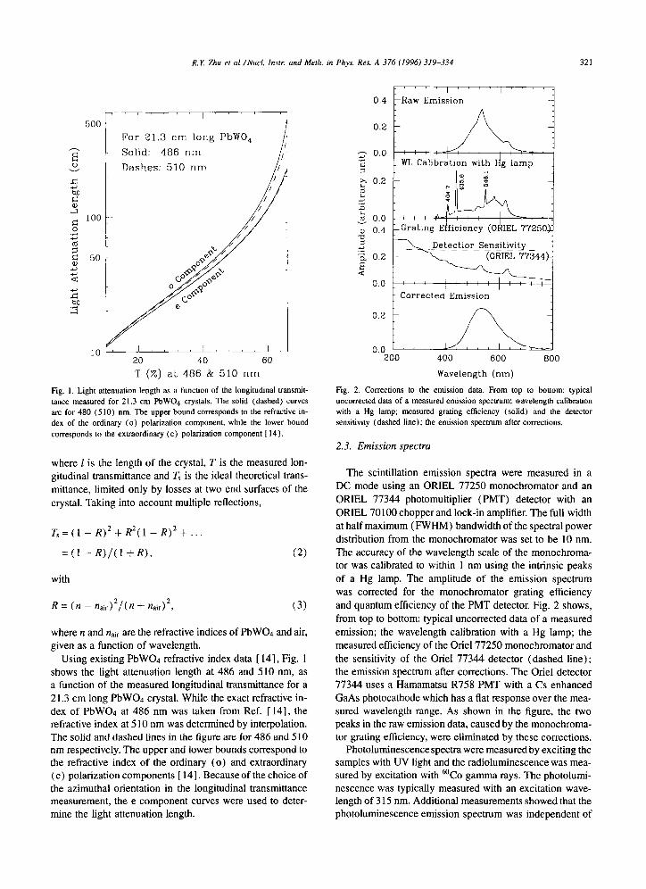
Fig. 2. Corrections to the emission data. From top to bottom: typical
uncorrected data of a measured emission spectrum; wavelength calibration
with a Hg lamp; measured grating efficiency (solid) and the detector
sensitivity (dashed line); the emission spectrum after corrections.
2.3. Emission spectra
The scintillation emission spectra were measured in a DC mode using an ORIEL 77250 monochromator and an
ORIEL 77344 photomultiplier (PMT) detector with an
ORIEL 70100 chopper and lock-in amplifier. The full width
at half maximum (FWHM) bandwidth of the spectral power distribution from the monochromator was set to be 10 nm. The accuracy of the wavelength scale of the monochroma- tor was calibrated to within 1 nm using the intrinsic peaks
of a Hg lamp. The amplitude of the emission spectrum was corrected for the monochromator grating efficiency
and quantum efficiency of the PMT detector. Fig. 2 shows,
from top to bottom: typical uncorrected data of a measured
emission; the wavelength calibration with a Hg lamp; the
measured efficiency of the Oriel77250 monochromator and
the sensitivity of the Oriel 77344 detector (dashed line); the emission spectrum after corrections. The Oriel detector 77344 uses a Hamamatsu R758 PMT with a Cs enhanced GaAs photocathode which has a flat response over the mea-
sured wavelength range. As shown in the figure, the two peaks in the raw emission data, caused by the monochroma- tor grating efficiency, were eliminated by these corrections.
Photoluminescencespectra were measured by exciting the samples with UV light and the radioluminescence was mea- sured by excitation with 6oCo gamma rays. The photolumi- nescence was typically measured with an excitation wave- length of 315 nm. Additional measurements showed that the photoluminescence emission spectrum was independent of

322 R. E Zhu et (II. /Nucl. Instr. and M&h. in Phys. Rex A 376 (19961319-334
excitation wavelength in the range from 250-350 nm. The radioluminescence spectra were typically measured at a dose
rate of 36 krad/h. It should be noted that when the emission spectra are measured in a DC mode, phosphorescence (or
afterglow) can give rise to a potential source of background.
This can be a particular problem for a weak scintillator if the intensity of the phosphorescence is higher than the in- trinsic scintillation. However, the phosphorescence was not
a problem for the dose rate and total doses used for these measurements.
2.4. Light yield, uniformity and decay times
The scintillation light yield at room temperature (23”) was measured using a Hamamatsu photomultiplier tube
(R2059 PMT) which has a bialkali photocathode and quartz window. A collimated y-ray source, such as 13’Cs or @Co,
was used to excite the small end of the crystal. The large end
of the crystal was coupled to the PMT with Dow Coming 200 or Viscasil600M silicone fluid. All other surfaces of the
crystal were wrapped with either one layer of Tyvek paper
or 5 layers of PTFE teflon film. The photoelectron numbers, corresponding to the y-ray peak, was determined by the peak ADC channel obtained by a Gaussian fit (not includ-
ing the Compton edge [ 1511, times a calibration constant corresponding to the number of photoelectrons per ADC
channel. The calibration was obtained by using the single
photoelectron peak, again from a Gaussian fit, and was cross-checked with an LED calibration, taking into account
the intrinsic width of the single photoelectron spectrum:
photoelectron number = [ 1 + ( rs,/Peaksp)2]
X ( PeakLan/ULeo ) ‘1 (4)
where, Peak and u are the peak and width from a Gaussian fit, and the subscripts LED and spe refer to the distributions
of LED and single photoelectron spectra, respectively.
The light response uniformity was measured by moving a
collimated y-ray source along the crystal at different longi-
tudinal positions and the result was fit to a linear function:
Ly/LY,id = 1 f 6(X - Xmid)/&nid,
where x is the distance from the small end, LYmid is the fit value of the light yield at the middle of the crystal, Amid, and
S is a measure of the light response uniformity. The decay constants of the the scintillation light were
measured using two independent methods: ( 1) an integra- tion method and (2) a single photon counting method [ 171. in the integration method, the photoelectron yield was mea- sured as a function of integration gate width up to 4 gs and the result was parametrized as
LY/LYtot = F + Si (1 - e-‘/‘I) + &( 1 - e-‘/r*), (6)
where LYt,, is the total light yield obtained from the fit, and F, Si and & are the normalized amplitudes of a fast
component with a decay time constant of less than N 10 ns,
and two slow components with decay time constants of TI and ~2 respectively. The normalization was done such that
F+S, +s2 G 1. (7)
In the single photon counting method, coincident gamma rays from a MC0 source were used to measure the decay time distribution of single photoelectrons produced by the
scintillation light in the crystal. The distribution was mea- sured relative to a fast start signal which was provided by a 1 in. diameter BaF2 crystal coupled to a Hamamatsu R5023
PMT which had rise time of 0.6 ns. The stop signal was
provided by a Hamamatsu R2059 PMT which was weakly coupled to the PbW04 sample in such a way that the av-
erage number of photoelectrons per gamma ray interaction
was very small (< 1). The decay times were measured out to 512 ns using a LeCroy 2228A TDC which had a resolu-
tion of 250 ps/channel. The resulting time distribution, after
the start peak, was parametrized as
cnom [Sa/7ae-‘17a + Sb/7be-“‘b + Sc/7ce-‘irC] , (8)
where S,, Sb and S, are the normalized amplitudes of the three decay components with time constants of ra, rb and rc respectively, and cnorm is an overall normalization factor.
It should noted that, because of the different time region
in these two measurements, the time constants and relative amplitudes determined by the differential and integral meth-
ods do not directly correspond with each other. The single photon counting method is best suited to determine the short
decay time components ( < 30 ns), but can give a poor esti-
mate of the amplitude of the longer decay times if either the average number of photoelectrons is too large, which can result in underestimating the amplitude of the slow compo-
nents, or because of poor statistics if the average number of photoelectrons is too small. On the other hand, the inte-
gration method cannot accurately measure the short decay
times because of the need to provide a minimum gate length for the ADC, but gives the best measure of the very long
decay time components. The two methods do agree in both the amplitudes and the decay times if two measurements were carried out in an identical time region. Therefore, they
complement each other by providing the best accuracy in measuring the two different regions of the spectrum. How- ever, it should be emphasized that in both cases, the fits are simply parameterizations of the data which are not unique, and do not necessarily represent the true decay times of the scintillation components in the crystal.
2.5. Thermoluminescence
The thermoluminescence (TL) spectra were obtained by exposing an approximately 10 mg sample of each crystal to 1 Mrad of @Co y-ray irradiation. The TL was measured 10 min after the irradiation from 40 to 400” at a heating rate of 2’/s. All measurements were made at a pressure of 760 mm in a

R.Y 2’~ et ol./Nucl. Instr. and Merh. in Phys. Res. A 376 (1996) 319-334 323
Fig. 3. We layout of the JPL irradiation facility, including the mCo y-ray
source and location of the PbWO4 samples.
helium atmosphere. The total thermoluminescence intensity, integrated over the emission spectrum, was measured using an EMI 9635QB phototube.
2.6. Phosphorescence
The radiation induced phosphorescence was determined by measuring the light output from the crystal shortly after irradiation with no further external excitation applied. Irra- diations were canied out at a high dose rate (34 kradlh) for cumulative doses of 0.7 and 1 .O Mrad, and at a low dose rate corresponding to the typical dose rate expected at the LHC ( 120 rad/h). The light output was measured by placing a Hamamatsu R2059 PMT immediately in front of the crystal and recording the phototube current as a function of time after irradiation. For measurements starting approximately 10 min after irradiation, the phototube current never ex- ceeded approximately 40 PA at a phototube voltage of 2500 V. However, for measurements starting l-5 s after irradia- tion, care had to be taken to prevent the phototube from be- ing exposed to excessively high currents during irradiation. Therefore, the high voltage was kept at a low value ( 1000 V) during irradiation, and was raised to 2000 V within a few seconds after irradiation to measure the current due to the phosphorescence. Under these conditions, the current in the phototube produced by light from the crystal, which was wrapped in white reflecting teflon, never exceeded approxi- mately 20 PA. The current produced in the phototube alone under the same conditions was less than 0.33 PA.
‘“M” HOTOTUBE FO
MEASUREMENTS
Fig. 4. The layour of the gamma ray irradiation facility at Brookhaven
National Laboratory.
The energy equivalent noise for the phosphorescence was determined from the phototube current and the known gain of the tube. The tube gain was measured using a method similar to that described in Section 2.4. The measured cur- rent divided by the gain of the phototube gives the number of photoelectrons produced per second due to the phospho- rescence. This can be converted into an energy equivalent noise using a nominal light output for the crystal of 10 pho- toelectrons per MeV measured by R2059 PMT.
2.7. Gamma ray irradiation
The gamma ray irradiations were carried out at two dif- ferent irradiation facilities in order to provide a cross check between different measurements. The first, shown in Fig. 3, was at the Jet Propulsion Laboratory (JPL) . It was equipped with an approximately 4000 Ci @Co source during this in- vestigation. Measurement equipment, such as monochroma- tors and phototubes, were placed inside the facility and sig- nals were brought out through feedthrough tubes to addi- tional equipment and computers outside the radiation area. The crystal samples, wrapped only with aluminum foil, were placed at a fixed distance in order to obtain a well defined dose within a fixed time, i.e. 1, 10 and 20 krad in one hour and 70 and 900 krad in 18 h, as illustrated in the figure. The dose rate was calibrated using a MDH 2025 Monitor with air-equivalent ion chambers which had an accuracy of 5%.
The second irradiation facility was the Gamma Ray Irra- diation Facility (GRIF) at Brookhaven National Lab. This

324 R. L Zhu ef al. /Nucl. Instr. and Meth. in Php. Rrs. A 376 (1996) 319-334
100
50
0
I 7 I : 728
I,,,, I I / ,-
: 767
: 768
I I , - I I 1 -
: 1015
200 400 600
Wavelength (nm)
800
Fig. 5. Longitudinal transmittance of five 21.3 cm PbW04 samples as a function of the wavelength.
facility, as shown in Fig. 4, consists of a 20000 Ci 6oCo source contained within a large UV-vis spectrophotometer which can be used to measure transmission and emission spectra before, during, and after irradiation [ 161. It was also used as a radiation source for the phosphorescence de- cay time and thermoluminescence measurements. The dose rate was calibrated using a Victoreen Model 525 electrom- eter/dosimeter which has an instrumental accuracy of l%, and agreed with the dose rate measured using LiF dosime- try to better than 5%. Samples irradiated here were prepared and irradiated under the same conditions as at JPL.
All procedures and measurements on the samples after ir- radiation were carried out in the dark or under red light in order to minimize any effects of optical bleaching. For the measurements made at GRIF, the samples were measured within 30 min after irradiation, while at JPL, the measure- ments were made within two hours after irradiation. For the light yield measurement, the samples were wrapped with either one layer of the Tyvek paper ( 140 ,um) , or five lay- ers of F’TFE film, consistent with the wrapping used before irradiation.
3. Results of measurements on optical properties
3.1. Transmittance and light attenuation length
Figs. 5 and 6 show spectra of the longitudinal trans- mittance of each sample measured before irradiation. The changes in transmittance after irradiation are discussed in
200 400 600
Wavelength (nm)
800
Fig. 6. Transmittance of five small size PbW04 samples as a function of wavelength. The light path is along the longest edge of the sample.
Section 4. There were no significant absorption bands at wavelengths longer than 500 nm. For most crystals, the transmittance at 800 nm was 2 70%, i.e. close to the theo- retical limit, indicating a very long light attenuation length at this wavelength. The only exception was crystal 1022, which was irradiated prior to these measurements, and has a transmittance below 70% at 800 nm. However, below 500 nm, the transmittance shows significant absorption. This ab- sorption causes the yellowish color described in Section 2.1. The exact origin of this absorption is not yet understood. There are also significant differences in the transmittance spectra in this wavelength region. While samples 767, 1015 and 1022 have a knee below 400 nm, samples 728 and 768 show none, and the latter have very poor transmittance at 370 nm. In addition, sample 767 has a higher transmittance at 370 nm than samples 1015 and 1022. The knee in the longitudinal transmittance at 370 nm seems to be correlated with the radiation hardness of the crystal, as discussed in Section 6.
All small samples show significantly better transmittance below 500 nm. It also is clear from Fig. 6 that SIC samples 34 and 41 have a very sharp rising edge at 340 nm, even though sample 34 has a longer path length than the other samples.
Table 2 lists the transmittance and the light attenuation length (LAL) at 486 and 5 10 nm for the five full size sam- ples calculated according to Eq. ( 1). Most crystals have a light attenuation length longer than 100 (50) cm at 510 (486) nm, except crystal 1022, which has a significantly

R.E Zhu et ul./Nucl. Instr. and Meth. in Phys. Res. A 376 (1996) 319-334 325
Table 2
Light attenuation length of PbW04 samples
ID
128 167 768 1015 1022
Transmittance [ %] @486 nm 64.9 55.2 51.2 49.3 46.1
LAL [cm] @486 nm 156 73 58 52 47
Transmittance [ 961 @510 nm 69.0 64.6 60.0 60.2 56.8 LAL [cm] @510 nm 259 152 98 100 79
shorter light attenuation length. The lower initial transmit-
tance and light attenuation length of sample 1022 can be
attributed to the fact that it was irradiated before it was re-
cerved, as discussed in Section 2.1.
3.2. Emission
Figs. 7 and 8 show the photoluminescence (solid curves) and radioluminescence (dashed curves) emission spectra.
These spectra were corrected for the grating efficiency and
detector sensitivity, as discussed in Section 2.3. The overall shape of most of the emission spectra is similar, and is close to a Gaussian distribution with a FWHM of about 120 nm.
However, sample 34 has a broader emission, and sample 478
has a narrower emission, as compared to the other samples.
For most samples, the radioluminescence seems to have a 20
to 30 nm blue shift, as compared to the photoluminescence. Fig. 9 shows the PbW04 emission spectrum together with
the quantum efficiencies of various photodetectors: a Hama-
400 500 600 700
Wavelength (nm)
Fig. 7. Photo- (solid) and radio- (dashes) luminescence of five full size PhW04 samples as a function of the wavelength.
10
5
0
5
0
5
0
5
0
1
o_ 400 500 600
Wavelength (nm)
Fig. 8. Photo- (solid) and radio- (dashes) luminescence of five small
PbW04 samples as a function of the wavelength.
matsu R2059 PMT, a Hamamatsu 2 cm* photodiode with sil-
icon oxide (S274403) and silicon nitrite (S2744-08) resin, and an EG&G avalanche photodiode ( APD) . The emission weighted quantum efficiencies of these devices are 10.4%,
64%. 77% and 81% for the R2059, S2744-03, S2744-08 and EG&G APD, respectively.
PbWO, Ermssion
O,._<. I I, I. I,, I O.O
300 400 500 600
Wavelength (nm)
Fig. 9. PbW04 emission and quantum efficiency of various photodetectors.

326 R.K Zhu er al./Nucl. Insrr. and Meth. in Phvs. Res. A 376 (1996) 319-334
1.2
1.0
6=1.7% I ’ 1 I.
I I
I i f - - -
f i 1 1.2 I ; : / ; I-
_ 767, 6=-0.9%
1 T I T T 7 T 1;
SIC 17 lL@-+-+ + + : G i L.Y.,., = 45 p.e./MeV
Y F=0.31 Sl=d29 S2=0.40
T1=69 ns s2=1600 ns 1
2 0.5
,a g 0.0
2 1.0
;3” 0.5
r 2 0.0
2 1.0
0.5
L.Y.,,, = 33 p.e./MeV
F=0.46 S1=0.30 S2=0.22
71=96 ns T2=1100 ns
1.2 I ; ; ; ; I
1022, 6=0.3% 0.0 1.0
t 1 j ’ ’ ’ II L
1.0 T 1 T _ T T 1 0.5
Bogoroditsk 476 t
L.Y.,,, = 41 p.e./MeV 1
F=0.60 s1=0.31 s2=0.09 1
rl=64 ns T2=6600 ns
0.8 I I-
O 100 200 0.0
Distance from Small End (mm) 0 2000 4000
Integration Time (ns)
Fig. 10. The light response uniformity of live full size PbW04 samples is Fig. 12. The light yield of five small size PbW04 samples as a function
shown as a function of the distance to the small end of the crystal. of integration time.
3.3. Light yield, decay time and response uniformity
Fig. 10 shows the light response uniformity measured before irradiation for the five full size samples. Samples 728,
1.0
0.5
0.0 1.0
2 0.5 a
2 0.0
2 1.0
3 0.5
: 2 0.0
z 1.0
0.5
0.0 1.0
0.5
0.0
F=0.41 51=0.40 S2= 0.19
rl=26 ns c?=500 ns
L.Y.,,, = 10 p.e./MeV
F=0.46 51=0.31 S2=0.21
rl=66 ns r2=1350 ns I , I I
0 2000 4000
Integration Time (ns)
Fig. 11. The light yield of five full size PbW04 samples is shown as a
function of integration time.
767 and 768 were wrapped with 5 layers of PTFE teflon film, while samples 1015 and 1022 were wrapped with one layer of Tyvek paper. The results were fit to Eq. (5) and show that the uniformity is generally better than a few percent for both types of wrappings. This good uniformity can be attributed to the fact that the light attenuation length at the emission peak (500 nm) is long enough to provide adequate compensation between the attenuation and focusing effect caused by the tapered shape [ 61.
Figs. 11 and 12 show the data for the light yield and decay time measurements determined using the integral method. The light yield as a function of integration time was fit to the parameterization given in Eq. (6) and the results are shown in the figures. The fits show that, over this time interval, the decay times can be parameterized as a sum of ( 1) a very fast
Table 3 Light yield (p.e./MeV) of PbW04 samples
ID LYtot LYxhls LYloons
728 12 9.0 9.8
767 10 6.1 7.0
768 II 5.3 6.7
1015 18 5.2 6.5
1022 13 4.1 5.9
10 42 14 16
17 45 21 25
34 33 20 23
41 78 28 33
478 41 30 34

R.E Zhu et al./Nucl. Instr. und Meth. in Phys. Rex. A 376 (1996) 319-334 321
10
1
1000
100
5EO III
2 lOA0
G 100
1000
loo 1 -
Time (ns)
Fig. 13. Decay time spectra measured with the single photon counting method for five full size samples.
component with a decay time of less than 10 ns, (2) a slow component with a decay time of 20 to 200 ns and (3) a very slow component with a decay time of 500 ns to several ,us.
Table 3 lists the total light yield (LYtO[ defined in Eq. (6)) and the light yield integrated in 50 (LYans) and 100 ( LYims) ns gates, in units of the number of pho- toelectrons per MeV of energy deposit (p.e./MeV). For full size samples, the fraction in the very slow component varies from 19% for undoped sample 728 to 48% for the more recently grown Nb-doped sample 1015. All Nb-doped samples have very similar light yields measured in the short gates (50 and 100 ns).
The light yield and decay time for the small samples vary considerably. All SIC samples have a significant very slow component (22 to 55%) in the total light output. However, sample 34, which was prepared with vacuum annealing and has a broad emission spectrum, has much smaller slow com- ponents, as compared to sample 41, which was prepared by annealing in an oxygen-rich atmosphere and has an emission in the green region. On the other hand, the Bogoroditsk sam- ple 478, which has a narrow blue emission, has the largest fast component (60%) and the smallest very slow compo- nent (9%). SIC sample 41 has the highest overall light yield (78 p.e./MeV), while its light yield measured in the short gates (50 and 100 ns) is similar to that of sample 478. Note the high photoelectron/MeV yield from samples 34 and 478 is partly due to the fact that their emission peaked at the region where R2059 PMT provides a higher quantum efti- ciency.
Fig. 13 shows the decay times measured using the single
photon counting technique for the five full size Bogoroditsk samples. The short decay times are characterized by two fast components. one with a time constant on the order of 2 ns, and another in the range from 8 to 17 ns. These components are consistent with the short to medium decay components found using the integral method. The single long component fit over this time interval (500 ns) is in the range from 350 to 500 ns, which is again consistent with the values found using the integral method. It is also clear that crystal 728, which is undoped, has the smallest slow components given by either method.
It should again be noted that in both the integral and sin- gle photon counting methods, the fitted parameters are not unique, nor is the parameterization. Fitting to two, three or even four exponential terms can all give good fits with very different values for the parameters. In addition, the fit range can greatly affect the parameters. Nevertheless, the short de- cay times are best measured by the single photon counting method, and the long decay times by the integral method. However, it should again be emphasized that these are sim- ply parameterizations to the data and do not necessarily rep- resent the actual scintillation decay times of the crystal.
4. Results on radiation damage
There are a number of possible effects of radiation dam- age in a scintillating crystal. These include radiation induced absorption (i.e. color center formation), a possible effect on the scintillation mechanism, and radiation induced phos- phorescence. Damage to the scintillation mechanism could affect the light yield, while color center formation would affect the light attenuation length of the crystal, and thus the light output observed by the photodetector. Radiation in- duced phosphorescence could cause additional noise in the readout device.
Only the full size samples were studied for radiation dam- age, since the results for a small sample would not necessar- ily be representative of the performance of a large crystal in situ at LHC [ 61. Only damage by electromagnetic energy deposition using 6oCo y-rays was measured in this investi- gation. Additional studies on radiation damage caused by neutrons and hadrons will be carried out in future.
4. I. Emission damage
Fig. 14 shows the radioluminescence of samples 767 and 1015 measured before (solid) and after (dashes) 1 Mrad of @Co y-ray irradiation at a dose rate of 36 krad/h. The spectra in the figure are arbitrarily normalized to facilitate a comparison of their shape. It is clear that there is no signifi- cant change in the shape of the emission spectra before and after irradiation. This indicates that the scintillation mecha- nism which gives rise to this spectral shape is not damaged by the radiation. However, it is more difficult to make any quantitative statement on the possible change in the absolute

328 R.K 2%~ et al./Nucl. Instr. and Mrrh. in Phw. Rrs. A 376 (1996) 319-333
0 300 400 500 600
Wavelength (nm)
Fig. 14. Photoluminescence spectra measured before (solid) and after
(dashes) 1 Mrad irradiation are shown as a function of wavelength for
samples 767 and 1015.
amplitude of the emission spectra before and after irradia-
tion, since absolute intensity is affected by the systematic
errors of the measurements and the radiation induced ab-
sorption in the samples.
4.2. Radiation induced phosphorescence
Fig. 15 shows the radiation induced phosphorescence in samples 767 and 768 as a function of time starting approx-
imately 10 min after y-ray doses of 700 and 1000 krad, re- spectively, which were accumulated at a dose rate of 3.4 x
lo4 rad/h. The apparent lower phosphorescence intensity in
768 was at least partly due to its higher induced absorption.
The decay time of the phosphorescence intensity can be fit
to two time constants: one with a decay time of about 6 to 7
min, and another with a longer decay time of about 42 min. For very short times after irradiation (starting within a few
seconds), the phosphorescence intensity was observed to be
considerably higher than after the first 10 min, but decayed away by several orders of magnitude within approximately one minute.
In order to simulate conditions more representative of the LHC, a piece of of crystal 767 (corresponding to approx- imately half the original volume) was irradiated at a dose rate of 120 rad/h. At this lower dose rate, the phospho- rescence measured immediately after irradiation reached a maximum after an exposure of only 10 min, which was con- siderably less than after the high dose rate exposure, and was essentially independent of total dose for longer exposures. This implies that, under low dose rate conditions, the rate at which conduction electrons are captured in traps reaches a value which is approximately equal to the rate at which electrons are thermally released from these traps and sub-
1000 900 800 700
600
2 .S 500
-z 400
E s 300
u
2 200
a
100 90 80 70
60
I” I ” ” I”” !
I / , I, I, 1 J 10 20 30 40
Time after lrradiaton (min)
Fig. 15. The phosphorescence intensity is shown as a function of time for
samples 767 and 768 after y-ray doses of 700 and 1000 krad, respectively,
at a dose rate of 3.4 x lo4 lad/h. The decay times can be fit to two time
constants: one, measured in both samples, of N 6-7 min, and another,
measured in sample 768, of N 42 min.
sequently produce luminescence. The intensity of the phos-
phorescence, in terms of energy equivalent noise, was deter-
mined for times between l-5 s after irradiation according to the procedure described in Section 2.6. The value obtained
for a full sized crystal under low dose rate conditions was 0.4 MeV within a 40 ns integration time, which is well be-
low the acceptable noise limit for a precision electromag-
netic calorimeter at the LHC. However, it should be noted that the magnitude of the phosphorescence can vary signif-
icantly from crystal to crystal, and therefore this should be
checked again for the actual crystals which are to be used
in the calorimeter.
4.3. Radiation induced absorption and light output loss
Fig. 16 shows the longitudinal transmittance as a func- tion of wavelength measured before and after a series of ir- radiations from a few krad to 0.8 to 1.0 Mrad for the five
full size samples. The top curve in each plot represents the transmittance before irradiation, as shown in Fig. 5, and the bottom curve represents the highest dose, as indicated in the figure. Note that, for samples 767, 1015 and 1022, the mid- dle curves are difficult to distinguish from the bottom curve, indicating a very small change in the longitudinal transmit- tance, as well as saturation after a dose of a few krad.
It is clear that these five samples can be divided into two groups: ( 1) samples 728 and 768 which show significant radiation induced absorption, (2) samples 767, 1015 and 1022 which show much less damage. The shape of the ra- diation induced absorption is also different between these

R. Y Zhu et al. /Nucl. Instr and Meth. in Phys. Rex A 376 (1996) 319-334 329
100
50
0
50
2 a 0
z 2 50 .3
E
z 0 2 e
50
0
50
t t-
L
L .c Tj 50
i
Oi 200 400 600 800
Wavelength (nm)
Fig. 16. Transmittance before and after irradiation as a function of
Fig. 17. The light attenuation length at 486 and 510 nm as a function of
cumulative dose for crystals 728. 767, 768, 1015 and 1022. The actual
doses are the same as in Fig. 16.
wave-
length with cumulative doses of (I) 2.4, 1 I, 20 and 834 krad for 728 and
768; (2) 1.0. 2.6, 7.6, 18.2, 28.2, 119 and 770 krad for 767; and (3) 2.
4. 5, 15, 35. 105 and 1000 krad for 1015 and 1022.
two groups. Significant absorption was found at wavelengths
longer than 600 nm for samples 728 and 768, while it is much less for 767, 1015 and 1022.
The longitudinal transmittance measurements can be
used to determine the light attenuation length according to Eq. ( 1). Fig. 17 shows the light attenuation length at 486
and 510 nm as a function of accumulated dose. As dis-
cussed in Section 3.2, the emission of these crystals peaks at around 5 10 nm.
The light attenuation length of crystal 728 and 768 de-
graded immediately after the first dose of 2.4 krad to 20 and 30 cm, respectively, and the degradation continued to
produce an attenuation length of less than 20 cm after the
highest dose for 768. On the other hand, the light attenua- tion lengths of 1015 and 1022 were roughly stable at 40 to 60 cm after a few krad up to a dose of 1 Mrad. For sample 767, the light attenuation length decreased to the range of 50 to 80 cm. It can be noted that the samples with better radiation resistance, namely 767, 1015 and 1022, initially
showed higher transmittance at 370 nm than samples 728 and 768, which showed poorer radiation resistance.
The light output, normalized to the mm-radiated value, is shown as a function of cumulative dose for crystals 767, 1015 and 1022 in Fig. 18. It follows a similar pattern to the light attenuation length. The degradation in light output after irradiation for samples 728 and 768 is not plotted because it was difficult to accurately measure the light output of these two crystals after the irradiation due to the large radiation
0
?I 0.0
b= 1.0 ;: 4
0.5 \ +u 7 jr 0.0
2 1.0
2
0.5
Dosage (krad)
Fig. 18. The light output normalized to the value before irradiation as a
function of cumulative dose for crystals 767. 1015 and 1022. The actual
doses are the same as in Fig. 16.

R.X Zhli et al./Nucl. Instr. and Mrth. in Phw. Res. A 376 (1996) 319-334
1001 I 1 I I1 / I Table 4
400 600 Wavelength (nm)
o.ot 1 ’ ’ 1 ’ ” 0 100 200
Time (h)
Fig. 19. Recovery from radiation at room temperature for sample 1015.
The curves are, from top to bottom: before irradiation, 170, 49 and 4.8 h
after 1 Mrad irradiation. Bottom figures show the recovery in transmittance,
light attenuation length and light yield with time. The rightmost data point
was taken after 40 days after 1 Mrad irradiation.
induced absorption and interference from the phosphores- cence. After the first 2 krad, the light output of 1015 and
1022 were reduced to 70% of their initial values, and then
leveled off at about 50 to 60% up to the full dose of 1 Mrad. The degradation in the light output of sample 767 was much smaller, dropping to 80% of its initial value.
In summary, the radiation induced absorption causes sig-
nificant degradation in the observed light output of the sam- ples measured. The better samples (767, 1015 and 1022)
showed saturation in their damage, which indicates the ori-
gin is most likely due to trace element impurities or de-
fects in the crystal. The best sample (767) shows much less degradation in light attenuation length and light output.
4.4. Spontaneous recovery at room temperature
Lead tungstate appears to show spontaneous recovery from radiation damage at room temperature. The top plot of Fig. 19 shows the recovery in the transmittance as a func- tion of wavelength for sample 1015 after a dose of 1 Mrad. The bottom plot of Fig. 19 shows the transmittance, light attenuation length at 486 and 5 10 nm, and normalized light yield as a function of time after a 1 Mrad irradiation. The solid line in the light yield plot is a fit to an exponential re- covery time with a time constant of 160 h, as shown in the figure. Note that the rightmost data point was taken after 40 days after 1 Mrad irradiation, as marked in the figure, and was included in the fit, which is shown as the horizontal bar
Optical bleaching and thermal annealing for sample 768
Operation Duration @486 nm @510 nm
[h] T IS] LAL [cm] T [%I LAL [cm]
Initial
After 840 krad
700 nm bleaching
700 nm bleaching
600 nm bleaching
600 nm bleaching
500 nm bleaching
Recovery @ RT
640 nm bleaching
200’ thermal
annealing
660 nm bleaching
- 51.2 58 60.0 98
- 21.0 17 24.0 19
6 27.5 21 32.4 26
12 32.7 26 38.5 33
6 45.6 44 54.1 67
12 49.0 52 58.1 86
6 44.6 42 53.6 65
24 45.6 44 54.5 68
6 49.2 52 59.1 92
2 52.9 63 62.5 120
6 51.5 59 61.5 110
across the data point. Similar recovery in the transmittance,
light attenuation length, and light output was also observed
for samples 728, 767, 768 and 1022.
4.5. Optical bleaching and thermal annealing
The radiation induced absorption can also be reduced by either optical bleaching or thermal annealing. It is known
that the color centers in crystals can often be entirely elimi-
nated by heating the crystal to a high temperature, a process know as thermal annealing [6]. By injecting light into the crystal, the color centers can also be eliminated by the pro-
cess of color center annihilation [ 201, and the effectiveness of this optical bleaching is known to be wavelength depen-
dent.
Optical bleaching and thermal annealing were also found to be effective for PbW04. A series of measurements were
carried out for samples 728, 768, 1015 and 1022. After a dose of 840 krad, bleaching light was applied at various
wavelengths, and then finally the crystal was placed in an
oven at 200’ for two hours. Table 4 lists the measured trans-
mittance and light attenuation length at 486 and 5 10 nm for
sample 768. It is interesting to note while light with a wave- length longer than 600 nm is indeed useful to bleach the sample, light at a wavelength of 500 nm actually causes the absorption in this wavelength range to increase, similar to the well known UV damage of BGO crystals. Fig. 20 shows the transmittance as a function of wavelength for sample 768.
Measurements with sample 728, 1015 and 1022 showed a similar result, i.e. light at wavelengths of 600 nm or longer was effective for optical bleaching.
4.6. Thermoluminescence
Fig. 21 shows thermoluminescence glow curves for sam- ples 767 and 768. The result shows that sample 768 has a much stronger TL response than 767, indicating a higher concentration of trapped charge and luminescent recombi- nation centers in sample 768. This observation is consistent

R.H Zhu et ai./Nucl. Instr. and Meth. in Phys. Res. A 376 (1996) 319-334 331
0
Initial 843 krad
700 nm. 6h
400 600 Wavelength (nm)
Fig. 20. The transmittance of sample 768 as a function of wavelength. The
curves correspond to: I - initial; 2 - 843 krad; 3 - 6 h optical bleaching
at 700 nm; 4 - I2 additional hours at 700 nm; 5 - 6 h at 600 run; 6 - I2
additional hours at 600 nm; 7 - 6 h at 640 nm; 8 - 2 h thermal annealing
at 2oo”c.
with the observation that sample 768 is less radiation hard
than sample 767. However, the TL signal in both samples is rather weak, and is roughly 3 to 4 orders of magnitude less intense than a typical BaF2 sample. The longer lived
I”” I”” I””
on _._ 0 100 200 300 400
Temperature (“C)
Fig. 21. Thermoluminescence glow curves for samples 767 and 768.
100 7 / ’ ’ I ’
SIC4 (&K1x45 mms)
c ~ G - 50
400 600
Wavelength (nm)
4011 7 ’ , * r’ ’ 7 1
0 1 2 3
Cumulated Dosage (krad)
Fig. 22. Top: the longitudinal transmittance as a function of wavelength
before and after irradiation for sample 4 from SIC (4.5 cm long). Bottom:
the light yield integrated in 30, 100 and 1090 ns is shown as B function of
cumulative dose.
phosphorescenceobserved in both crystals most likely arises
from the two lowest temperature glow peaks. While sample
768 has at least three peaks at 110, 150 and 245’, sample
767 has only two peaks at 90 and 140”. These data indicate that the lowest temperature trap has a depth of about 0.7 eV
for both crystals, but to estimate the trap depth for the other peaks would require additional measurements.
4.7. Intrinsic radiation resistance
Finally, there is evidence that PbW04 crystals can be
made radiation hard, or that PbW04 crystals are intrinsi-
cally radiation hard. The sample 767 is one example which
showed only a 20% degradation in light yield. Fig. 22 shows the transmittance as a function of wavelength (top) and the light output as a function of integrated dose for a diameter 3 x 4.5 cm sample (SIC4, which was not included in the original group), for a low dose test. This particular sample was grown by the Czochralski method using raw materials with adequate purity (99.9 to 99.99%). The radiation dam- age in both the absorption and the light output are negligible. Although this is a small crystal, the performance of this par- ticular sample provides evidence that the radiation damage problem of PbW04 crystals can be resolved through a sys- tematic research and development program, as is currently being pursued by the CMS collaboration.

332 R.E Zhu et ol./Nucl. Ins~. and Meth. in Phys. Res. A 376 (19961 319-334
Table 5
GDMS analysis result on trace element concentrations (ppm)
Sample
Na Al Si K Ca Nb MO Ba TM RE
128 3.2 < 2.6 < 0.7 < 0.3 5.5 3.9 8.9 0.82 < 1.0 0.28
767 9.3 < 0.7 42 0.50 0.97 7.8 16 0.40 < 0.4 0.1 I
768 1.8 < 0.7 51 0.52 2.4 6.9 15 0.51 < 0.4 0.12
1015 2.8 3.0 1.5 1.9 5.5 7.9 120 0.16 1.8 0.1 I
1022 3.1 3.0 1.8 1.7 7.1 IO 100 0.16 1.6 0.10
34 3.0 2.0 1.3 3.3 2.7 < 0.002 14 I .o 1.3 0.18
41 1.7 13 0.8 3.4 IO < 0.001 18 3.8 1.4 0.15
478 1.8 3.5 3.0 2.5 1.3 2.4 4.6 0.24 1.2 0.13
5. Results on material characterization
As shown in the previous two sections, the characteris-
tics of the PbW04 crystals measured in this study, such as
transmittance, emission spectra, decay times and radiation resistance, vary considerably from sample to sample. Ma- terial characterization, including determination of trace el-
ement impurities, defects and structural analysis, can help to provide information on these various properties. In this investigation, an initial attempt has been made to identify
possible deviations from stoichiometric PbW04 for sample
768, and to identify trace element impurities in a number of the other samples. All material characterization was per-
formed by the independent analysis firm of Charles Evans and Associates [ 2 11.
A quantitative wavelength dispersive Electron Microprobe
(EMPA) analysis was done on sample 768, and Particle In- duced X-ray Emission (PIXE) analyses were performed on samples 767 and 768, to identify possible deviations from stoichiometric PbW04. The results showed that these crys- tals were essentially pure stoichiometric PbWO4. However,
there was an indication that the W/Pb ratio decreased by up to 5% from the small end to the large end in both crystals.
Glow Discharge Mass Spectroscopy (GDMS) was used
to search for trace element impurities in all five large samples
and three small samples: SIC 34, SIC 41 and Borogoditsk 478. A survey of 77 elements revealed impurities at the
few ppm to sub-ppm level in all samples. Table 5 lists the impurities detected in a portion of each sample, taken 3 to 5 mm below the surface of the crystal, i.e. no surface contamination. All detected impurities at a level greater than 1 ppm are listed, in addition to the sum of the transition metals (TM): SC, Ti, V, Cr, Mn, Fe, Co, Ni, Cu and Zn, and the sum of detected rare earth elements (RE) : Ce, Pr, Nd, Eu, Sm, Gd, Tb, Dy, Ho, Er, Tm, Yb and Lu. The transition metals and rare earth elements were found to be adversely
affect the radiation resistance of BGO and BaF2, respectively
[61. From the GDMS analysis, the following observations can
be made: - All samples from Bogoroditsk have significant Nb and
MO, while samples from SIC have no detectable Nb.
- The trace element MO seems to be related to the slow
scintillation components, e.g. sample 478 and 728 have
the lowest MO content.
- There seems to be no obvious correlation between the
detected trace element impurities and the susceptibility to radiation damage, indicating that defects, such as oxygen vacancies, may play an important role in determining the
radiation hardness. However, it should be noted that GDMS is essentially a
bulk analysis technique which detects only those impurities
which are contained a small sample. It is possible that higher concentrations of impurities are present in certain localized
areas, or inclusions, in the crystals. This was, in fact, the case
for BaF2 [ 61. Other analytical techniques, such as Secondary Ionization Mass Spectroscopy (SIMS), can be employed
to better determine if such effects are present in PbW04
crystals.
6. Summary and discussion
6.1. Optical properties
The longitudinal transmission of full size PbW04 crys-
tals from Bogoroditsk shows significant absorption below 500 nm, as shown in Fig. 5. However, since the scintillation
emission is peaked at 500 nm, these crystals provide accept-
able light attenuation lengths and light response uniformity. This explains the excellent energy resolution with a constant term of less than 0.5% obtained in CERN beam tests [ I]. The blue absorption of full size crystals, however, may still present a serious problem, since it prevents the propagation of the blue light in the crystal. As discussed in Section 3.3, the blue light has a short decay time, and is thus more de- sirable for a fast calorimeter. In addition, there seems to be a correlation between the absorption at 370 nm and the ra- diation hardness of the crystal, as discussed in Section 4. It is thus important to understand its origin, and to eliminate the blue absorption in full size crystals.
All full size PbW04 crystals from Bogoroditsk have a ra- dioluminescence which is peaked at 500 nm, and a 20 to 30 nm blue shift as compared to the photoluminescence, as
R.Y. Zhu et al./Nucl. Instr. and M&h. in Phys. Res. A 376 (1996) 319-334 333
shown in Fig. 7. Measurements on small crystals from SIC and Bogoroditsk, however, show that some crystals have an emission peaked in the blue region, and they have smaller very slow components, as shown in Figs. 8 and 12. This ob- servation agrees with previous results [ 181. Our measure- ments also confirm an early observation that the emission of PbWO4 crystals may be affected by different annealing pro- cesses in crystal growth [ 191, The samples annealed in vac- uum ( SIC 34) and in an oxygen-rich atmosphere (SIC 41) indeed have different emission peaks. This indicates that the blue and the green luminescence centers in the PbW04 are possibly structure or oxygen content related. However, the change in absorption, i.e. the shift of the absorption edge to longer wavelengths, may also cause an apparent shift of the emission spectrum, if the intrinsic scintillation of PbW04 crystal contains both blue and green components.
The total light yield of full size PbW04 crystals, integrated in a 100 ns gate, is up to 10 p.e./MeV, as measured by a PMT with a bialkali photocathode (Hamamatsu R2059). It can be converted to - 100 photons/MeV, assuming the emission weighted quantum efficiency is 10.4%, as shown in Fig. 9.
The decay time of the scintillation light from PbW04 can be parameterized by three components: one fast ( < 10 ns), one slow (20 to 200 ns), and one very slow (500 ns to a few ps), as shown in Figs. 11, 12 and 13. The fraction of the very slow component was observed to be larger for recently grown full size PbW04 crystals, although all have similar light yields measured with 50 and 100 ns gates. For crystals which have their main emission peak in the blue region (Bogoroditsk 478 and SIC 34), the fraction of the very slow component is significantly less than those with their emission peaked in the green region. Since the slow component is not useful for LHC applications, and the residual slow component from previous beam crossings could introduce additional readout noise, it is desirable to understand the origin of the slow component and to minimize it by optimizing the crystal growth process.
6.2. Radiation damage
As shown in Section 4, it appears that PbW04 crystals are intrinsically radiation hard, but currently produced pro- duction size PbWO4 crystals suffer from radiation damage at different levels. The scintillation mechanism seems to be unaffected by irradiation with 6oCo y-rays up to 1 Mrad, and the effect of radiation induced phosphorescence seems to not have serious consequences in situ at the LHC. The main consequence of radiation damage for PbW04 is the ra- diation induced absorption, or color center forma&ion. This absorption causes a degradation of the transmittance and light attenuation length, and hence the detectable light out- put. It should be pointed out that the CMS PbW04 crystal calorimeter is more sensitive to the color center formation than what has been shown in this investigation. This is due to the fact that the average path length of light collected by a
small area avalanche photodiode ( APD) is longer than that by a PMT covering the entire back face of the crystal [ 231. The APD readout thus is more sensitive to the change in light attenuation length caused by color center formation.
The five full size crystals can be divided into two groups: ( 1) samples 728 and 768, which show significant radiation induced absorption and significant degradation in light out- put, (2) samples 767, 1015 and 1022 which show much less damage. The radiation resistance seems to be correlated with the longitudinal transmittance at 370 nm. While crys- tals 728 and 768 have very low transmittance at 370 nm, crystals 767,1015 and 1022 have a knee below 400 nm, and sample 767 has the highest transmittance at 370 nm.
The degradation of the transmittance, light attenuation length and the light output saturates after a few krad. This indicates that the radiation damage observed in PbW04 is related to intrinsic impurities or defects, and that the radi- ation does not create additional defects. For crystals with better radiation resistance, the reduced light output is about 50 to 80% of the initial value, which is still adequate for a precision calorimeter at LHC. However, the damage recov- ers at room temperature with a time constant of about 160 h, which would cause a serious problem with a time-dependent response in situ, and thus affect the stability of the calorime- ter. This can be compared to performance of BaFz crystals, whose damage saturated at a few krad, but does not recover at room temperature [ 221.
It is also important to note that, although the change of transmittance or light attenuation length (and thus the light output) can be calibrated in situ by an appropriate light monitoring system, the change in light attenuation length, however, may destroy the light response uniformity. The consequence of a degraded light response uniformity is a degraded energy resolution which can not be corrected by the monitoring system [ 221. It is thus important to reduce the magnitude of the saturated radiation damage in PbWO4 by reducing damage related impurities and defects as much as possible.
Optical bleaching and thermal annealing were found to be effective in removing bleachable color centers in the crystal. Although thermal annealing is not practical in situ, optical bleaching, in principle, could be implemented by sharing the same optical fiber system used for light monitoring and calibration [ 241. This was the solution for production BaF2 crystals to be used to construct a precision calorimeter at the SSC [ 221. However, the ultimate solution would be to improve the crystal quality to a level where the radiation damage is negligible. Optical bleaching in situ would then only be used as a last resort, if improvements in the crystal quality were no longer possible or cost effective.
6.3. Material characterization
The identification of impurities, defects and structural changes are crucial for PbW04 crystal development, since they are possibly responsible for the blue absorption, the

334 R.E Zhu et al./Nucl. lnstr. and Mrth. in Phy. Res. A 376 (1996) 319-334
slow decay components and the susceptibility to radiation damage. Our analysis indicates that some impurities. such as MO, may be responsible for the slow components. How- ever, there seems to be no obvious correlation between the detected trace element impurities and the susceptibility to radiation damage, indicating an important role of defects, such as oxygen vacancies, in these processes, or that impu- rities may exist in inclusions.
Further analysis in this aspect is certainly an important part of the PbW04 development program. In developing radiation-hard BaF2 crystals, various analytical techniques were used, including PIXE, EMPA, GDMS, Secondary Ionization Mass Spectroscopy (SIMS), Atomic Absorp- tion Spectrum (AAS), Rutherford Back Scattering (RBS) , Electron Spin Resonance (ESR), Electron-Nuclear Dou- ble Resonance (ENDOR), Neutron Activation Analysis (NAA), Transmission Electron Microscopy (TEM) and Scanning Electron Microscopy (SEM). It is important that all necessary characterization means be used to establish a correlation between the crystal performance and impurities and defects in the crystals.
7. Conclusions
Since the discovery of PbW04 as a scintillating crystal, much work has been devoted to ( 1) production of large, calorimeter-sized crystals, (2) understanding their perfor- mance and (3) improvements in crystal quality, especially radiation resistance. The investigation described in this re- port is an integrated part of this effort. At this time, pro- duction size crystals can be mass produced at Bogoroditsk and SIC, and the quality of these crystals approach what is required by the CMS collaboration at LHC. There are, however, existing problems in production size crystals, such as the blue absorption, the slow components and the time- dependent performance under irradiation. A rigorous R&D program, including crystal evaluation and material analy- sis, is necessary to understand the origin of these effects, and to reduce or eliminate these problems. It is expected that PbW04 crystals capable of providing a stable, preci- sion electromagnetic calorimeter for CMS at the LHC will be developed as a result of this R&D program.
Acknowledgements
We would like to thank Dr. P Lecoq for providing PbW04 samples grown in Bogoroditsk and Prof. Z.W. Yin for pro- viding PbWO4 samples grown at SIC. Many inspiring and interesting discussions with Drs. E. Auffray, B. Borgia, 1. Dalinei, P. Denes, M. Kobayashi, M. Korzhik, P. Lecoq, M. Schneegans, J. Virdee and Z.W. Yin are also acknowledged.
References
[ I] Compact Muon Solenoid Technical Proposal. CERN/LHCC 94-38,
LHCC/PI (1994).
[ 21 L* Letter of Intent to the SSC Laboratory, November 1990.
[ 31 GEM Letter of Intent, SSCL SR- 1184, November I99 1.
141 CompactMuonSolenoidLetterofIntent.CERN/LHCC92-3,LHCC/Il
(1992).
[S] L3P Letter of Intent, CERN/LHCC 92-5, LHCC/I3 (1992).
161 G. Gratta, H. Newman and R.Y. Zhu, Annu. Rev. Nucl. Part. Sci. 44
(1994) 453.
[ 71 Crystal Clear Collaboration, see S. Anderson et al.. Nucl. Instr. and
Meth.A332(1993)373.
[S] M. Kobayashi et al., Nucl. Instr. and Meth. A 333 ( 1993) 429.
[ 91 0. Buyanov et al., Nucl. Instr. and Meth. A 349 ( 1994) 62;
S. Inabaet al., Nucl. Instr. and Meth. A 359 ( 1995) 485;
G. Alexeev et al., Nucl. Instr. and Meth. A 364 ( 1995) 307.
[ IO] J.P. Peigneux, Nucl. Instr. and Meth. A 351 197 (1994).
[ I I ] P. Lecoq et al.. Nucl. Instr. and Meth. A 365 ( 1995) 291.
[ 121 See. forexample,presentationsgiven by M. Kobayashietal., P Lecoqet
al. andC. Woodyetal.,in: InorganicScintilfatorsandtheir Applications,
eds. P. Dorenbos and C.W. van Eijk (Delft University Press, 1995).
[ 131 D.A. Ma and R.Y. Zhu, Nucl. Insu. and Meth. A 333 (1993) 422.
[ 141 G. Bakhshiva and A. Morozov, Sov. J. Opt. Technol. 44 ( 1977) 9.
[ 151 S. Baccaro et al.. CMS TN/95065, June 1995.
[ I61 I?W. Levy, J. Phys. Chem. Solids 52 (1991) 319.
[ 171 L.M. Bollinger and GE. Thomas, Rev. Sci. Instr. 32 ( 1961) 44.
] 181 M. Kobayashi et al., in: Inorganic Scintillators and their Applications,
eds. P. Dorenbos and C.W. van Eijk (Delft University Press, 1995) p.
286.
[ 191 Z.W. Yin et al.. in: Inorganic Scindllators and their Applications, eds.
P. Dorenbos and C.W. van Eijk (Delft University Press, 1995) p. 490.
[ 201 D.A. Ma and R.Y. Zhu. Nucl. Insu. and Meth A 332 (1993) 113.
[ 211 Charles Evans and Associates, 301 Chesapeake Drive, Redwood City,
CA 94063, USA.
[ 221 R.Y. Zhu, Nucl. Instr. and Meth. A 340 ( 1994) 442.
[ 231 R.Y. Zhu. Ray-tracing for PbWOp crystals, talk given in CMS ECAL
Meeting, August 9, 1995.
[24] D.A. Ma, R.Y. Zhu and H. Newman, Nucl. Instr. and Meth. A 356
(1995) 309.