Embed Size (px)
Citation preview
A System for Evaluating Performance and
Cost of SIMD Array Designs∗
Martin C. Herbordt Jade Cravy Renoy Sam
Owais Kidwai Calvin Lin
Department of Electrical and Computer EngineeringUniversity of Houston, Houston, TX 77204-4793
EMail: [email protected] Phone: (713) 743-4434
Note: This article has been accepted for publication in the Journal of Parallel and Distributed Computing as of
October 25, 1999.
Abstract: SIMD arrays are likely to become increasingly important as coprocessors in domain specific systems as
architects continue to leverage RAM technology in their design. The problem this work addresses is the efficient
evaluation of SIMD arrays with respect to complex applications while accounting for operating frequency and chip
area. The underlying issues include the size of the architecture space, the lack of portability of the test programs,
and the inherent complexity of simulating up to hundreds of thousands of processing elements. The overall method
we use is to combine architecture level and Electronic Design Automation (EDA) level modeling by using an EDA
based tool to calibrate architectural simulations. The resulting system retains much of the high throughput of
the architecture level simulator but also has accuracy similar to that of an early pass EDA synthesis and circuit
simulation. The particular problem of computational cost of the architectural level simulation is addressed with
a novel approach to trace-based simulation (we call trace compilation) which we find to be one to two orders
of magnitude faster than instruction level simulation while still retaining much of the accuracy of the model.
Furthermore, traces must be generated for only a small fraction of the possible parameter combinations. Using
trace compilation also addresses program portability by allowing the user to code in a single data parallel language
with a single compiler, regardless of the target architecture. We have used our system to evaluate thousands of
potential SIMD array designs with respect to real applications and present some sample results.
Keywords: SIMD Architecture, Parallel Computer Architecture, Computer Design Evaluation, Computer Simu-
lation, Domain Specific Systems, Virtual Prototyping
∗This work was supported in part by the National Science Foundation through CAREER award #9702483, by the Texas Advanced
Research Program (Advanced Technology Program) under grant #003652-952, and by a grant from the Compaq Computer Corporation.
1
1 Introduction
Since the mid-1990s SIMD arrays have reappeared as designers have begun to leverage memory technology in much
the same way as MIMD designers have been leveraging microprocessor technology since the mid-1980s [6, 10, 13,
21, 23, 36]. The next five years should provide tremendous opportunities as it becomes possible to get an entire
non-trivial SIMD array onto a single substrate thereby mitigating the signal propagation issues that have been one
of the major technological difficulties. Even current designs have largely solved this problem, however: a board
level instruction issue rate of 100MHz was achieved in 1995 by Bolotski’s Abacus [3] and systems with a chip level
issue rate of 200MHz are commercially available from PixelFusion [28]. The likely applications continue to be
graphics [28, 36] and vision [4, 10, 24, 21] although compression [41], neural nets [23], chess (the IBM Deep Blue
coprocessors), and scientific computing [32] are some of the other possibilities.
Corresponding to the increased capabilities of single chip (or single substrate) SIMD arrays is an increase in
design choices; yet, no adequate tools exist that enable the designer to evaluate the complex hardware-software
interactions of this domain. According to Dung and Madisetti [5]: “The first 10% of the design cycle determines
nearly 80% of a system’s cost. Yet designers currently make early, crucial design choices in an unstructured and
unsupported system design environment.” Although our priorities differ from theirs, it is such a tool that we seek to
provide for evaluating performance and cost of SIMD-based systems with complex data parallel application codes
and large arrays of PEs.
Two methods are commonly used to model hardware-software interaction: architecture-level simulators and
Electronic Design Automation (EDA) tools. Architecture-level methods are good at providing high-level information—
especially about network congestion and cache behavior—when most of the system is well understood but less so
if it is not. The latter situation often occurs exactly in systems which provide solutions to problems not easily
addressed entirely with off-the-shelf components. Architecture-level methods are also weak in providing feedback
about the timing consequences of design changes. On the other hand, EDA tools allow the designer to get from
behavioral specification to physical device with little intervention. However, EDA tools are far from the preferred
method for architecture analysis: they are much too slow to give the “look-and-feel” of a real machine. For example,
evaluation of complex signal processing systems can take weeks of processing time on a farm of workstations.
We combine the two methods in the ENvironment for PArarallel Systems Simulation ANd Tools (ENPAS-
SANT). The architecture-level simulator provides a cycle-level model of the interaction between applications and
basic array components such as number of PEs and register file size. We use an EDA-based tool to generate oper-
ating frequencies, chip areas, and numbers of cycles for non-critical-path instructions. These are combined under
the framework of an EXCEL-based report generator.
The wide range of possible designs and scope of what we seek to automate results in a large number of design
requirements:
• Workload. Match the domain workload precisely by running real application programs.
• Accuracy. Match the target machine performance to the level of hardware generated by an early pass
synthesis.
• Domain coverage. Simulate as many machines as possible within the class of SIMD arrays.
• Simulator throughput. Evaluate the set of possible designs with respect to a particular application test
suite within a few days.
• Programmability of workload. The largest cost in benchmark studies involving prototypes is often coding
applications for machines with different instruction sets. Our constraint is to use a single portable data parallel
1
language and reuse all applications with little or no recoding.
• Fairness. Account for differences in program/architecture mapping, including algorithm selection.
• Flexibility. Target machines must be easy to specify and the hardware must be generated automatically.
Our major result is that, by using a series of novel ideas detailed below, we have created an evaluation
environment that largely meets these goals. We demonstrate this by presenting results from the evaluation of several
hundred designs with respect to the Image Understanding Benchmark, an application which requires execution of up
to several hundred million instructions depending on the array size. We have also analyzed many other applications
in computer vision, computational biochemistry, and solving partial differential equations, but will present those
results elsewhere. The results were generated on a workstation in a few days days processing time, or the time it
takes to do a single complex synthesis. The accuracy of the timing results is at the level of a partially tuned input
to a synthesis system as is appropriate for initial design exploration.
The major contribution of this work is a system for the rapid evaluation of SIMD array designs, accounting
for operating frequency and chip area, with respect to non-trivial applications. Particularly important for SIMD
arrays is the area output: this is because it determines the number and granularity of PEs that can fit on a chip.
This is absolutely critical as it allows us to answer basic questions as to what kinds of coprocessors are likely to be
available when, and with respect to which applications they are likely to be cost-effective.
There are four fundamental ideas behind our work. The first is to use only a single programmer’s model to
cover the entire class of SIMD arrays. To make this work without introducing the tremendous inefficiencies that
can be caused by a mismatch between programmer’s model and target machine requires two pieces of software: one
provides emulations of features present on some, but not all, machines; the other contains critical domain-specific
functions.
The second idea is what we call trace compilation. Application codes are not compiled directly to the target
machine instruction sets; rather, they are run on a generic SIMD array virtual machine emulator. In the process a
“coarse-grained” trace is generated. This trace is then refined through a series of transformations wherein greater
resolution is obtained with respect to the details of the target architecture. This process has two benefits: 1) virtual
machine emulation and trace compilation together are one to two orders of magnitude faster than simulating a
SIMD array at the instruction level, and 2) once a trace has been generated, it can be reused to evaluate a large
number of design alternatives.
The third idea is to use a commercial spreadsheet for the template and model specification and for report
generation. The advantages of spreadsheets for report generation are obvious, but they are also the perfect tool for
keeping track of machine parameters and automatically propagating constraints through complex interactions.
The fourth is to use a high level language program to generate the designs in the Verilog high level design
language. This simplifies version management and the outputs themselves.
The rest of this article is organized as follows. We next present an overview of the architectures of interest
and the issues in modeling them. There follow the software and hardware models themselves. After that come an
overview of the evaluation system, the details of the fundamental ideas behind it, some sample results, and the
conclusions.
2
2 SIMD Array Design Space
2.1 Design Alternatives in Current SIMD Machines
SIMD array systems are asymmetric: in their simplest configuration they have a general purpose processor, which
acts as a controller, and an array consisting of from a few hundred to a few hundred thousand processing elements
(PEs). In a simplified view of SIMD operation, the PEs execute synchronously instructions broadcast by the
controller while the controller is responsible not only for driving the array but also for executing the primary
thread of control. For details about many aspects of SIMD array architecture see, e.g., [31]. We now give an
overview of SIMD array system design issues.
PE design
One characteristic of SIMD arrays is that PEs do not have individual micro-sequencers or much other control
circuitry; rather their ‘CPUs” consist almost entirely of datapath. A wide range of PEs has been implemented:
the MGAP built at Penn. St. does not have even a complete one-bit ALU [22] while the MasPar MP2 contains
a 32-bit datapath and extensive floating point support [27]. PEs with two to four stage pipelines appear to be
natural extensions (see below and [1, 3]).
PE Memory Hierarchy
Another characteristic of SIMD arrays is that the PEs reference their own registers and memory in lock-step,
that is, all of the PEs operate on the same (corresponding) register and/or memory location at the same time.
Some designs have local addressing autonomy where the memory location of the PE operand is determined, at
least partially, by the contents of a PE register. Sizes of the memory hierarchy components have varied greatly
depending on the granularity of the array and the available technology. Recent fine grained machines such as the
Abacus [3] and the MGAP have only a few bytes of on chip memory per PE but perhaps a few thousand bytes per
PE off chip. A recent RAM based system, the NEC IMAP [9], has 1KB of on chip memory and 64KB of off chip
memory per PE. Also, although no SIMD array has yet been built with PE cache, studies have shown its clear
benefits [1, 18] so that is a possible future direction.
PE Nearest Neighbor Communication
Almost all SIMD arrays have communication links among physically adjacent PEs. Since PEs are usually laid out
in either one or two dimensions, the resulting network is usually either a one or two dimensional mesh or torus.
The latter is often called a NEWS network for the North/East/West/South directions. In systems where all of the
PEs are on a single chip, the communication latency of the nearest-neighbor network among neighboring PEs is
similar to the latency of a PE’s on-chip operand fetch. The path width of the nearest neighbor network is often
the same as the PE datapath width, although it may be substantially smaller.
General Communication
Many SIMD arrays have additional interPE communication networks. These have included the CM-2 packet
switched network, which supports broadcast, reduction, and scans [34]; the MasPar circuit switched network [2];
and various networks based on broadcast buses [8, 20, 25, 29, 39]. Nearly all of these networks have the property
that the communication takes from a few to a few thousand PE instruction cycles during which time the PEs are
idle.
Feedback from Array to Controller
Nearly all SIMD array systems have a mechanism to summarize array information through a global OR mechanism.
This allows the host to query the array to find out, e.g., whether any PE has found a result. Foster and Weems have
demonstrated the benefits to associative processing of a feedback mechanism that counts responding PEs [7, 37].
3
This latter feature was available in the Clip-4 [8] and the CAAPP [37], among others.
Array Instruction Issue
Building a system where the PEs run at maximum possible speeds requires very careful attention to instruction
issue and distribution. This problem is complicated if, as is generally the case in current designs, the host is a
microprocessor and the PE array is comprised of one or more Application Specific Integrated Circuits (ASICs).
There are three issues: i) the speed at which instructions can be issued, ii) the latency of the instruction from the
issuer to the PEs, and iii) the skew in instruction distribution to the various PEs in the array.
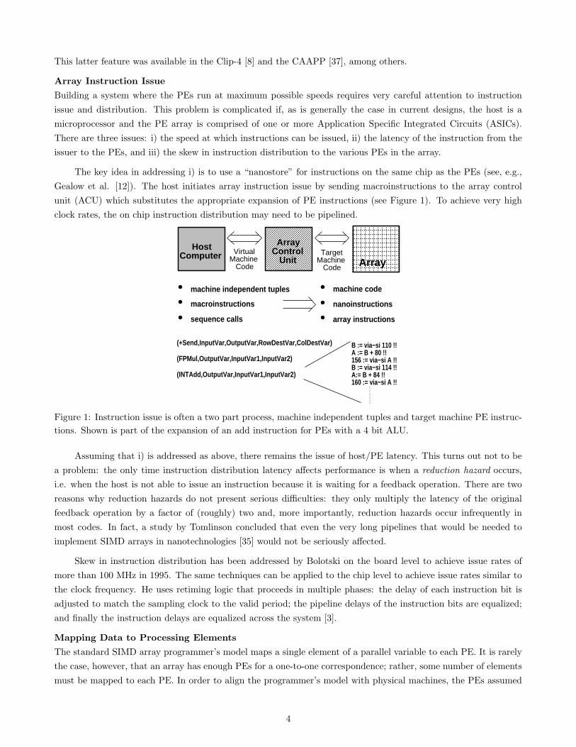
The key idea in addressing i) is to use a “nanostore” for instructions on the same chip as the PEs (see, e.g.,
Gealow et al. [12]). The host initiates array instruction issue by sending macroinstructions to the array control
unit (ACU) which substitutes the appropriate expansion of PE instructions (see Figure 1). To achieve very high
clock rates, the on chip instruction distribution may need to be pipelined.
HostComputer
ArrayControl Unit Array
VirtualMachine Code
TargetMachine Code
machine code
nanoinstructions
array instructionssequence calls
macroinstructions
machine independent tuples
(+Send,InputVar,OutputVar,RowDestVar,ColDestVar)
(FPMul,OutputVar,InputVar1,InputVar2)
(INTAdd,OutputVar,InputVar1,InputVar2)
B := via−si 110 !!A := B + 80 !!156 := via−si A !!B := via−si 114 !!A:= B + 84 !!160 := via−si A !!
. . . . .
. . . . .
. .
Figure 1: Instruction issue is often a two part process, machine independent tuples and target machine PE instruc-
tions. Shown is part of the expansion of an add instruction for PEs with a 4 bit ALU.
Assuming that i) is addressed as above, there remains the issue of host/PE latency. This turns out not to be
a problem: the only time instruction distribution latency affects performance is when a reduction hazard occurs,
i.e. when the host is not able to issue an instruction because it is waiting for a feedback operation. There are two
reasons why reduction hazards do not present serious difficulties: they only multiply the latency of the original
feedback operation by a factor of (roughly) two and, more importantly, reduction hazards occur infrequently in
most codes. In fact, a study by Tomlinson concluded that even the very long pipelines that would be needed to
implement SIMD arrays in nanotechnologies [35] would not be seriously affected.
Skew in instruction distribution has been addressed by Bolotski on the board level to achieve issue rates of
more than 100 MHz in 1995. The same techniques can be applied to the chip level to achieve issue rates similar to
the clock frequency. He uses retiming logic that proceeds in multiple phases: the delay of each instruction bit is
adjusted to match the sampling clock to the valid period; the pipeline delays of the instruction bits are equalized;
and finally the instruction delays are equalized across the system [3].
Mapping Data to Processing Elements
The standard SIMD array programmer’s model maps a single element of a parallel variable to each PE. It is rarely
the case, however, that an array has enough PEs for a one-to-one correspondence; rather, some number of elements
must be mapped to each PE. In order to align the programmer’s model with physical machines, the PEs assumed
4
Chip 1996 1999 2002
DRAM 64Mb 256Mb 1GbSRAM 4Mb 16Mb 64MbIMAP 64 8 bit PEs 256 16 bit PEs 256 32 bit PEs[10] 2Mb SRAM/ 8Mb SRAM/ 32Mb SRAM/
4KB per PE 4KB per PE 16KB per PE12 GP Registers, Multiplier Multiplier & FPALU, Shifter, GP registers,NN logic, etc. comm. etc.
Table 1: Shown are features in the current NEC IMAP SRAM-based chip and extrapolation with respect to
semiconductor industry projections.
by the programmer’s model (referred to as virtual PEs or VPEs) are emulated by the physical PEs. This emulation
can either be done entirely in software, through hardware support in the array control unit (ACU), or through a
combination of the two. This process is explained in detail in [15].
2.2 Extrapolated SIMD Machines
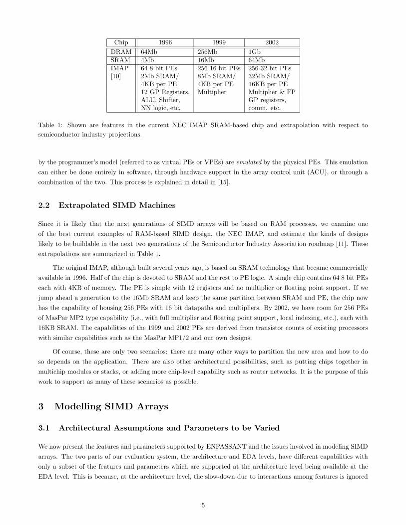
Since it is likely that the next generations of SIMD arrays will be based on RAM processes, we examine one
of the best current examples of RAM-based SIMD design, the NEC IMAP, and estimate the kinds of designs
likely to be buildable in the next two generations of the Semiconductor Industry Association roadmap [11]. These
extrapolations are summarized in Table 1.
The original IMAP, although built several years ago, is based on SRAM technology that became commercially
available in 1996. Half of the chip is devoted to SRAM and the rest to PE logic. A single chip contains 64 8 bit PEs
each with 4KB of memory. The PE is simple with 12 registers and no multiplier or floating point support. If we
jump ahead a generation to the 16Mb SRAM and keep the same partition between SRAM and PE, the chip now
has the capability of housing 256 PEs with 16 bit datapaths and multipliers. By 2002, we have room for 256 PEs
of MasPar MP2 type capability (i.e., with full multiplier and floating point support, local indexing, etc.), each with
16KB SRAM. The capabilities of the 1999 and 2002 PEs are derived from transistor counts of existing processors
with similar capabilities such as the MasPar MP1/2 and our own designs.
Of course, these are only two scenarios: there are many other ways to partition the new area and how to do
so depends on the application. There are also other architectural possibilities, such as putting chips together in
multichip modules or stacks, or adding more chip-level capability such as router networks. It is the purpose of this
work to support as many of these scenarios as possible.
3 Modelling SIMD Arrays
3.1 Architectural Assumptions and Parameters to be Varied
We now present the features and parameters supported by ENPASSANT and the issues involved in modeling SIMD
arrays. The two parts of our evaluation system, the architecture and EDA levels, have different capabilities with
only a subset of the features and parameters which are supported at the architecture level being available at the
EDA level. This is because, at the architecture level, the slow-down due to interactions among features is ignored
5
and so feature combinations are easier to specify and evaluate. At the EDA level, however, the combinations
have to make sense physically since we actually create workable designs and generate technology specific gate-level
netlists.
What never varies
What we never vary is i) the SIMD assumption, ii) support for the programmer’s model described in the next
section, iii) activity control, and iv) that PEs all contain a small amount of ROM to indicate edge and ID.
What can be modeled at the architecture level
We list the most important features and parameters that can be modeled. Many accept a size and a latency. First
inside the PEs:
• PE datapath from 1 to 64 bits
• Floating point and double precision units, possibly shared among PEs
• Multiplier and/or divider
• Nearest neighbor communication network parameters including path width
• Number of internal buses and ports in the register file
• Local indexing
• Per PE caching
• Simple pipelined PE datapaths
At the array level:
• Array size from 256 to 16 million PEs
• Load/store mechanism
• Communication networks including support for CM-2 type send, scans, broadcast, and reductions, as well as
region broadcast operations as found in machines such as the Clip-4 [8] and the CAAPP [39].
• Feedback including OR and Count.
EDA level restrictions
In order for EDA design parameterization to be beneficial, it must save significant engineering effort in creating
a wide variety of implementations. In the case of the present domain, some sacrifice must be made to the overall
quality of the design: you just would not do everything the same way when designing a 1 bit PE as you would a 32
bit PE. Among the compromises is a restriction on the combination of features. Other restrictions are as follows.
First, the internal architecture contains single input and output data buses. Previous studies indicated that
there is little benefit to having a third bus [18], although this addition would not be difficult. Second, we have
only three multiplier configurations: none, full output with half-width input, and half output with full-width input.
Again, these are the most cost-effective. Note that these design decisions are quite different from what would be
made for a microprocessor: the difference is in the benefit of trading off datapath area for cache versus trading
off datapath area for more processors or registers. The datapaths supported at the EDA level are summarized in
Table 2.
6
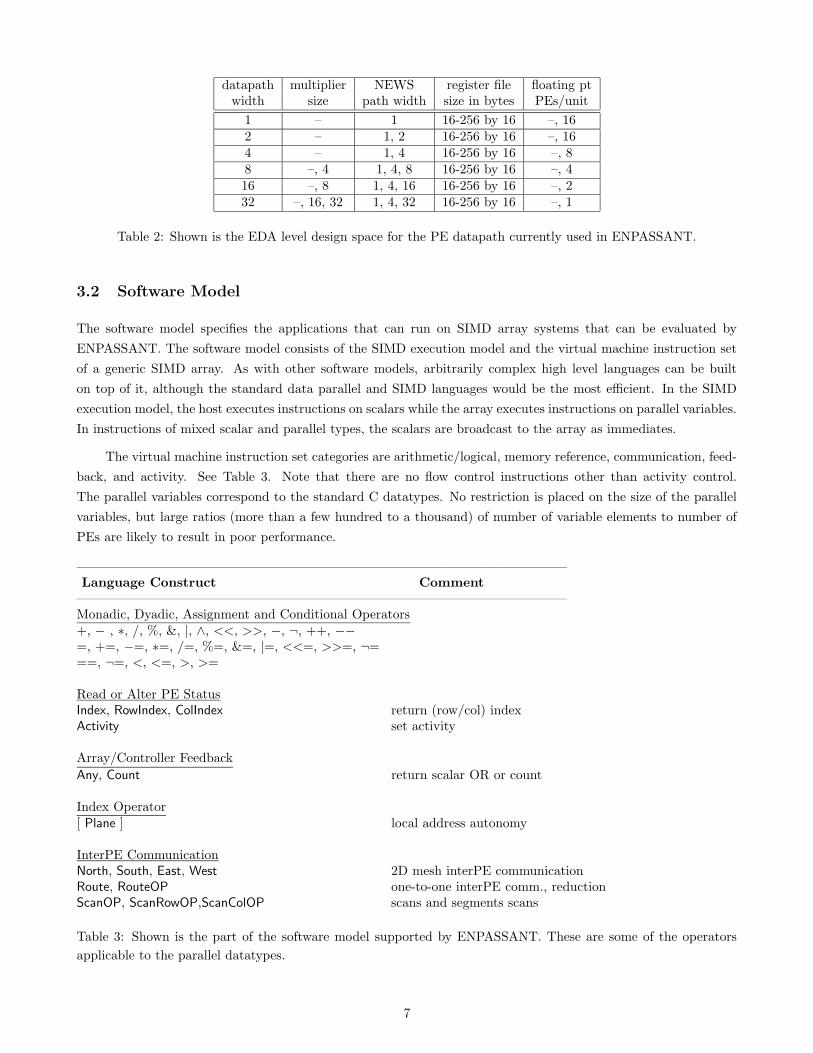
datapath multiplier NEWS register file floating ptwidth size path width size in bytes PEs/unit
1 – 1 16-256 by 16 –, 162 – 1, 2 16-256 by 16 –, 164 – 1, 4 16-256 by 16 –, 88 –, 4 1, 4, 8 16-256 by 16 –, 416 –, 8 1, 4, 16 16-256 by 16 –, 232 –, 16, 32 1, 4, 32 16-256 by 16 –, 1
Table 2: Shown is the EDA level design space for the PE datapath currently used in ENPASSANT.
3.2 Software Model
The software model specifies the applications that can run on SIMD array systems that can be evaluated by
ENPASSANT. The software model consists of the SIMD execution model and the virtual machine instruction set
of a generic SIMD array. As with other software models, arbitrarily complex high level languages can be built
on top of it, although the standard data parallel and SIMD languages would be the most efficient. In the SIMD
execution model, the host executes instructions on scalars while the array executes instructions on parallel variables.
In instructions of mixed scalar and parallel types, the scalars are broadcast to the array as immediates.
The virtual machine instruction set categories are arithmetic/logical, memory reference, communication, feed-
back, and activity. See Table 3. Note that there are no flow control instructions other than activity control.
The parallel variables correspond to the standard C datatypes. No restriction is placed on the size of the parallel
variables, but large ratios (more than a few hundred to a thousand) of number of variable elements to number of
PEs are likely to result in poor performance.
—————————————————————————————————————Language Construct Comment—————————————————————————————————————Monadic, Dyadic, Assignment and Conditional Operators+, − , ∗, /, %, &, |, ∧, <<, >>, −, ¬, ++, −−=, +=, −=, ∗=, /=, %=, &=, |=, <<=, >>=, ¬===, ¬=, <, <=, >, >=
Read or Alter PE StatusIndex, RowIndex, ColIndex return (row/col) indexActivity set activity
Array/Controller Feedback
Any, Count return scalar OR or count
Index Operator[ Plane ] local address autonomy
InterPE CommunicationNorth, South, East, West 2D mesh interPE communicationRoute, RouteOP one-to-one interPE comm., reductionScanOP, ScanRowOP,ScanColOP scans and segments scans
Table 3: Shown is the part of the software model supported by ENPASSANT. These are some of the operators
applicable to the parallel datatypes.
7
3.3 Parameterized Hardware Model
We had the following requirements when designing the parameterized EDA hardware model:
1. The model should be usable for generating operating frequencies and chip areas of the designs.
2. The instruction sets should efficiently implement the software model.
3. The model should support as much as possible the same specifications as the architecture level evaluator.
4. The model should lead to workable designs after synthesis, place-and-route, etc.
The last requirement is a case of not giving in to the temptation of simply adding up component areas and
measuring a few critical paths. We have found that even relatively simple designs can be surprisingly subtle and
have substantial ‘glue logic’ requirements.
We did not, however, try to model entire SIMD array systems at the EDA level. In particular we do not model
components that are similar for all designs and that need to be worked out largely at the place-and-route level.
These include instruction issue, clock tree, and memory system interface. Also, explicitly modeling in hardware
the various dedicated routers is best done independently for reasons given in Section 3.4. See [18, 17] for details of
that work.
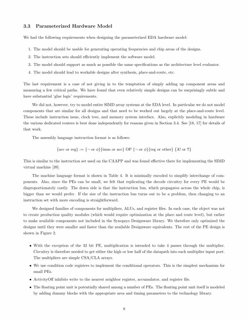
The assembly language instruction format is as follows:
{acc or reg} := {¬ or φ}{imm or acc} OP {¬ or φ}{reg or other} {A! or !!}
This is similar to the instruction set used on the CAAPP and was found effective there for implementing the SIMD
virtual machine [39].
The machine language format is shown in Table 4. It is minimally encoded to simplify interchange of com-
ponents. Also, since the PEs can be small, we felt that replicating the decode circuitry for every PE would be
disproportionately costly. The down side is that the instruction bus, which propagates across the whole chip, is
bigger than we would prefer. If the size of the instruction bus turns out to be a problem, then changing to an
instruction set with more encoding is straightforward.
We designed families of components for multipliers, ALUs, and register files. In each case, the object was not
to create production quality modules (which would require optimization at the place and route level), but rather
to make available components not included in the Synopsys Designware library. We therefore only optimized the
designs until they were smaller and faster than the available Designware equivalents. The rest of the PE design is
shown in Figure 2.
• With the exception of the 32 bit PE, multiplication is intended to take 4 passes through the multiplier.
Circuitry is therefore needed to get either the high or low half of the datapath into each multiplier input port.
The multipliers are simple CSA/CLA arrays.
• We use condition code registers to implement the conditional operators. This is the simplest mechanism for
small PEs.
• ActivityOff inhibits write to the nearest neighbor register, accumulator, and register file.
• The floating point unit is potentially shared among a number of PEs. The floating point unit itself is modeled
by adding dummy blocks with the appropriate area and timing parameters to the technology library.
8
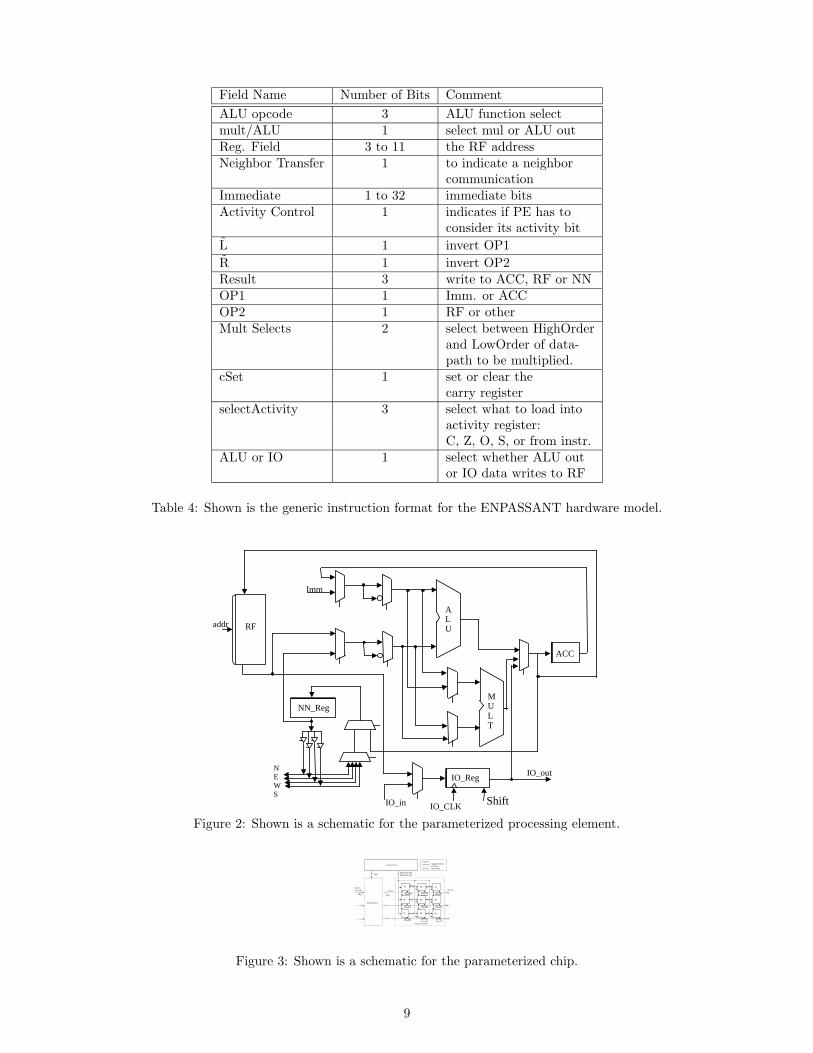
Field Name Number of Bits Comment
ALU opcode 3 ALU function selectmult/ALU 1 select mul or ALU outReg. Field 3 to 11 the RF addressNeighbor Transfer 1 to indicate a neighbor
communicationImmediate 1 to 32 immediate bitsActivity Control 1 indicates if PE has to
consider its activity bit
L̃ 1 invert OP1
R̃ 1 invert OP2Result 3 write to ACC, RF or NNOP1 1 Imm. or ACCOP2 1 RF or otherMult Selects 2 select between HighOrder
and LowOrder of data-path to be multiplied.
cSet 1 set or clear thecarry register
selectActivity 3 select what to load intoactivity register:C, Z, O, S, or from instr.
ALU or IO 1 select whether ALU outor IO data writes to RF
Table 4: Shown is the generic instruction format for the ENPASSANT hardware model.
IO_CLK
ACC
Imm
ALU
NN_Reg
NEWS
IO_in Shift
IO_out
MULT
IO_Reg
RFaddr
Figure 2: Shown is a schematic for the parameterized processing element.
IO_in IO_out
WDP
WNN
Control Unit
Instruction andimmediate dataAddr
Data Memory
Array Processor
PEData In(IO_out)
WDP
PE PE
PE PEPE
PEPEPE
IO_reg
Legend:Neighbor WiresIO WiresInstruction
IO_reg IO_reg
IO_reg
IO_reg IO_reg IO_reg
IO_reg
IO_reg
Figure 3: Shown is a schematic for the parameterized chip.
9
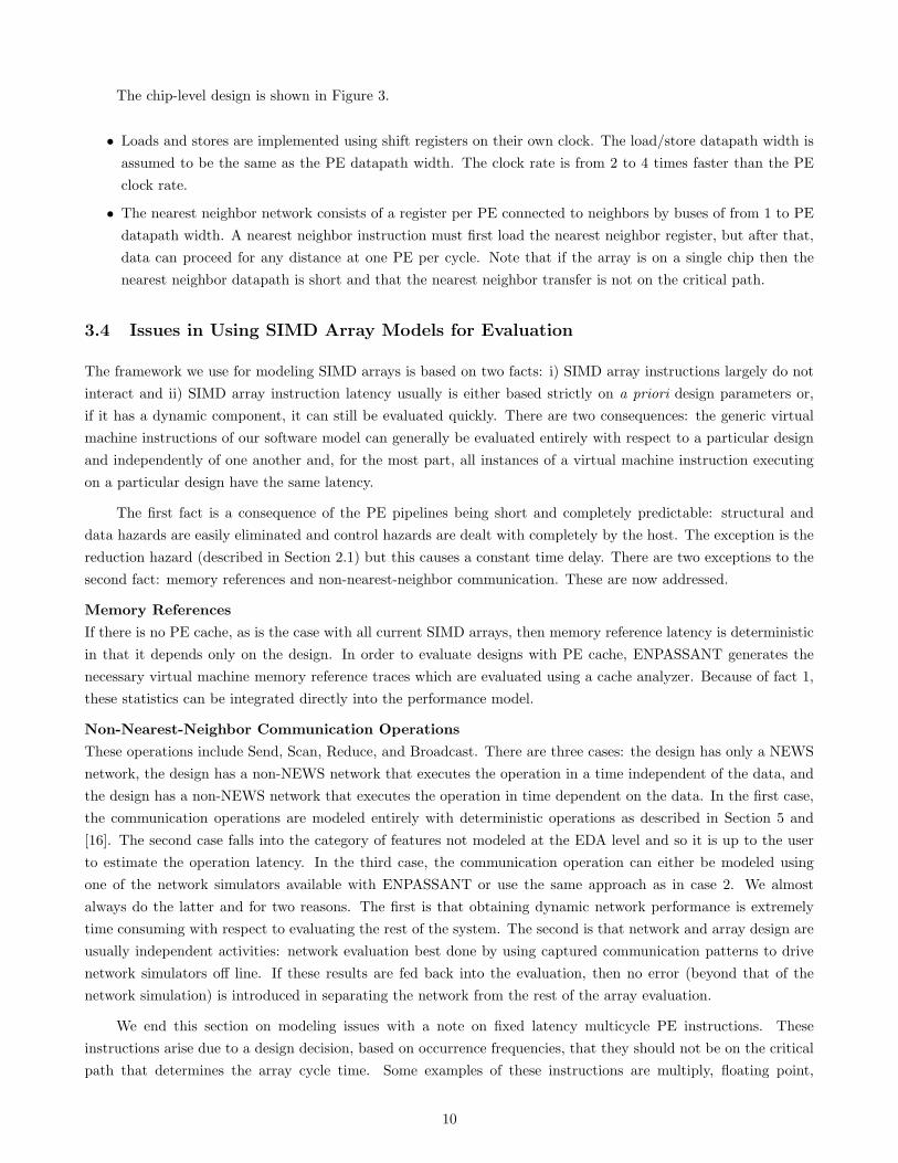
The chip-level design is shown in Figure 3.
• Loads and stores are implemented using shift registers on their own clock. The load/store datapath width is
assumed to be the same as the PE datapath width. The clock rate is from 2 to 4 times faster than the PE
clock rate.
• The nearest neighbor network consists of a register per PE connected to neighbors by buses of from 1 to PE
datapath width. A nearest neighbor instruction must first load the nearest neighbor register, but after that,
data can proceed for any distance at one PE per cycle. Note that if the array is on a single chip then the
nearest neighbor datapath is short and that the nearest neighbor transfer is not on the critical path.
3.4 Issues in Using SIMD Array Models for Evaluation
The framework we use for modeling SIMD arrays is based on two facts: i) SIMD array instructions largely do not
interact and ii) SIMD array instruction latency usually is either based strictly on a priori design parameters or,
if it has a dynamic component, it can still be evaluated quickly. There are two consequences: the generic virtual
machine instructions of our software model can generally be evaluated entirely with respect to a particular design
and independently of one another and, for the most part, all instances of a virtual machine instruction executing
on a particular design have the same latency.
The first fact is a consequence of the PE pipelines being short and completely predictable: structural and
data hazards are easily eliminated and control hazards are dealt with completely by the host. The exception is the
reduction hazard (described in Section 2.1) but this causes a constant time delay. There are two exceptions to the
second fact: memory references and non-nearest-neighbor communication. These are now addressed.
Memory References
If there is no PE cache, as is the case with all current SIMD arrays, then memory reference latency is deterministic
in that it depends only on the design. In order to evaluate designs with PE cache, ENPASSANT generates the
necessary virtual machine memory reference traces which are evaluated using a cache analyzer. Because of fact 1,
these statistics can be integrated directly into the performance model.
Non-Nearest-Neighbor Communication Operations
These operations include Send, Scan, Reduce, and Broadcast. There are three cases: the design has only a NEWS
network, the design has a non-NEWS network that executes the operation in a time independent of the data, and
the design has a non-NEWS network that executes the operation in time dependent on the data. In the first case,
the communication operations are modeled entirely with deterministic operations as described in Section 5 and
[16]. The second case falls into the category of features not modeled at the EDA level and so it is up to the user
to estimate the operation latency. In the third case, the communication operation can either be modeled using
one of the network simulators available with ENPASSANT or use the same approach as in case 2. We almost
always do the latter and for two reasons. The first is that obtaining dynamic network performance is extremely
time consuming with respect to evaluating the rest of the system. The second is that network and array design are
usually independent activities: network evaluation best done by using captured communication patterns to drive
network simulators off line. If these results are fed back into the evaluation, then no error (beyond that of the
network simulation) is introduced in separating the network from the rest of the array evaluation.
We end this section on modeling issues with a note on fixed latency multicycle PE instructions. These
instructions arise due to a design decision, based on occurrence frequencies, that they should not be on the critical
path that determines the array cycle time. Some examples of these instructions are multiply, floating point,
10
feedback, and memory reference with a simple memory hierarchy. Modeling multicycle operations is a two step
process: first the absolute latency is obtained using the hardware analyzer (see Section 7) and second, once the
cycle time has been computed, the absolute latency is converted to the number of cycles.
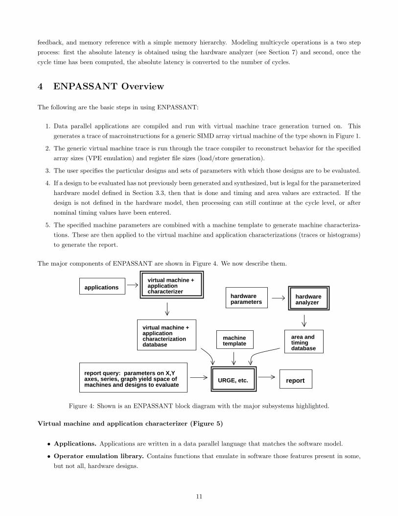
4 ENPASSANT Overview
The following are the basic steps in using ENPASSANT:
1. Data parallel applications are compiled and run with virtual machine trace generation turned on. This
generates a trace of macroinstructions for a generic SIMD array virtual machine of the type shown in Figure 1.
2. The generic virtual machine trace is run through the trace compiler to reconstruct behavior for the specified
array sizes (VPE emulation) and register file sizes (load/store generation).
3. The user specifies the particular designs and sets of parameters with which those designs are to be evaluated.
4. If a design to be evaluated has not previously been generated and synthesized, but is legal for the parameterized
hardware model defined in Section 3.3, then that is done and timing and area values are extracted. If the
design is not defined in the hardware model, then processing can still continue at the cycle level, or after
nominal timing values have been entered.
5. The specified machine parameters are combined with a machine template to generate machine characteriza-
tions. These are then applied to the virtual machine and application characterizations (traces or histograms)
to generate the report.
The major components of ENPASSANT are shown in Figure 4. We now describe them.
reportreport query: parameters on X,Yaxes, series, graph yield space ofmachines and designs to evaluate
applicationshardwareparameters
URGE, etc.
hardwareanalyzer
virtual machine +applicationcharacterizationdatabase
machinetemplate
area andtimingdatabase
virtual machine +applicationcharacterizer
Figure 4: Shown is an ENPASSANT block diagram with the major subsystems highlighted.
Virtual machine and application characterizer (Figure 5)
• Applications. Applications are written in a data parallel language that matches the software model.
• Operator emulation library. Contains functions that emulate in software those features present in some,
but not all, hardware designs.
11
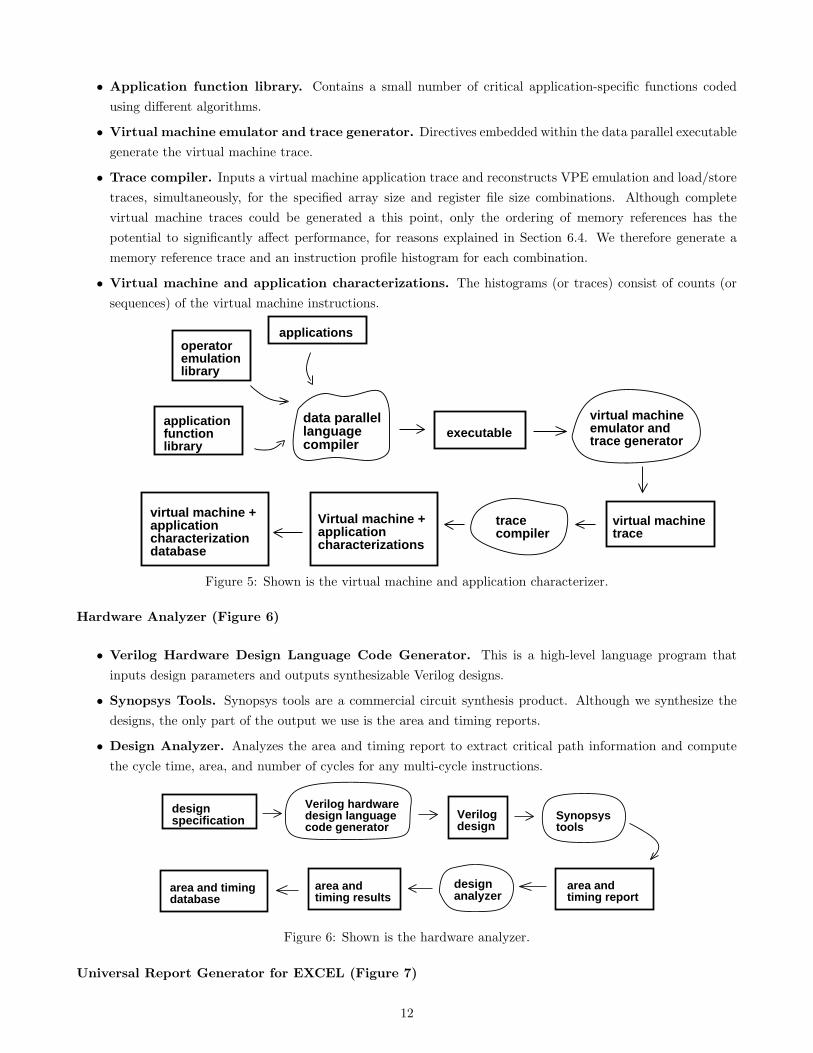
• Application function library. Contains a small number of critical application-specific functions coded
using different algorithms.
• Virtual machine emulator and trace generator. Directives embedded within the data parallel executable
generate the virtual machine trace.
• Trace compiler. Inputs a virtual machine application trace and reconstructs VPE emulation and load/store
traces, simultaneously, for the specified array size and register file size combinations. Although complete
virtual machine traces could be generated a this point, only the ordering of memory references has the
potential to significantly affect performance, for reasons explained in Section 6.4. We therefore generate a
memory reference trace and an instruction profile histogram for each combination.
• Virtual machine and application characterizations. The histograms (or traces) consist of counts (or
sequences) of the virtual machine instructions.
applications
executable
virtual machinetrace
applicationfunctionlibrary
operatoremulationlibrary
virtual machine +applicationcharacterizationdatabase
data parallellanguagecompiler
virtual machineemulator andtrace generator
tracecompiler
Virtual machine +applicationcharacterizations
Figure 5: Shown is the virtual machine and application characterizer.
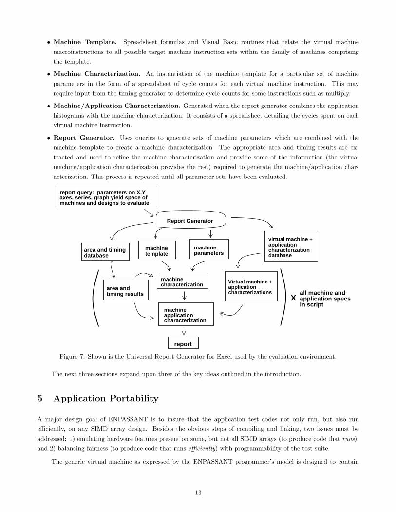
Hardware Analyzer (Figure 6)
• Verilog Hardware Design Language Code Generator. This is a high-level language program that
inputs design parameters and outputs synthesizable Verilog designs.
• Synopsys Tools. Synopsys tools are a commercial circuit synthesis product. Although we synthesize the
designs, the only part of the output we use is the area and timing reports.
• Design Analyzer. Analyzes the area and timing report to extract critical path information and compute
the cycle time, area, and number of cycles for any multi-cycle instructions.
designspecification
designanalyzer
Verilog hardwaredesign languagecode generator
Synopsystools
area andtiming report
area andtiming results
area and timingdatabase
Verilogdesign
Figure 6: Shown is the hardware analyzer.
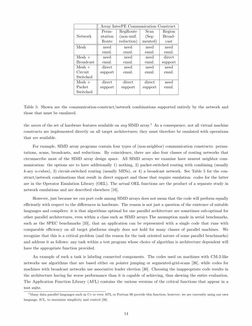
Universal Report Generator for EXCEL (Figure 7)
12
• Machine Template. Spreadsheet formulas and Visual Basic routines that relate the virtual machine
macroinstructions to all possible target machine instruction sets within the family of machines comprising
the template.
• Machine Characterization. An instantiation of the machine template for a particular set of machine
parameters in the form of a spreadsheet of cycle counts for each virtual machine instruction. This may
require input from the timing generator to determine cycle counts for some instructions such as multiply.
• Machine/Application Characterization. Generated when the report generator combines the application
histograms with the machine characterization. It consists of a spreadsheet detailing the cycles spent on each
virtual machine instruction.
• Report Generator. Uses queries to generate sets of machine parameters which are combined with the
machine template to create a machine characterization. The appropriate area and timing results are ex-
tracted and used to refine the machine characterization and provide some of the information (the virtual
machine/application characterization provides the rest) required to generate the machine/application char-
acterization. This process is repeated until all parameter sets have been evaluated.
report
machinecharacterization
machineparameters
machineapplicationcharacterization
report query: parameters on X,Yaxes, series, graph yield space ofmachines and designs to evaluate
Xall machine andapplication specsin script
virtual machine +applicationcharacterizationdatabase
Virtual machine +applicationcharacterizations
area andtiming results
area and timingdatabase
machinetemplate
Report Generator
Figure 7: Shown is the Universal Report Generator for Excel used by the evaluation environment.
The next three sections expand upon three of the key ideas outlined in the introduction.
5 Application Portability
A major design goal of ENPASSANT is to insure that the application test codes not only run, but also run
efficiently, on any SIMD array design. Besides the obvious steps of compiling and linking, two issues must be
addressed: 1) emulating hardware features present on some, but not all SIMD arrays (to produce code that runs),
and 2) balancing fairness (to produce code that runs efficiently) with programmability of the test suite.
The generic virtual machine as expressed by the ENPASSANT programmer’s model is designed to contain
13
Array InterPE Communication ConstructPerm- RegRoute Scan Region
Network utation (non-unif. (Seg- Broad-Route reduction) mented) cast
Mesh need need need needemul. emul. emul. emul.
Mesh + need need need directBroadcast emul. emul. emul. supportMesh + direct need need needCircuit support emul. emul. emul.SwitchedMesh + direct direct direct needPacket support support support emul.Switched
Table 5: Shown are the communication-construct/network combinations supported entirely by the network and
those that must be emulated.
the union of the set of hardware features available on any SIMD array.1 As a consequence, not all virtual machine
constructs are implemented directly on all target architectures; they must therefore be emulated with operations
that are available.
For example, SIMD array programs contain four types of (non-neighbor) communication constructs: permu-
tations, scans, broadcasts, and reductions. By coincidence, there are also four classes of routing networks that
circumscribe most of the SIMD array design space. All SIMD arrays we examine have nearest neighbor com-
munication: the options are to have additionally 1) nothing, 2) packet-switched routing with combining (usually
k-ary n-cubes), 3) circuit-switched routing (usually MINs), or 4) a broadcast network. See Table 5 for the con-
struct/network combinations that result in direct support and those that require emulation: codes for the latter
are in the Operator Emulation Library (OEL). The actual OEL functions are the product of a separate study in
network emulations and are described elsewhere [16].
However, just because we can port code among SIMD arrays does not mean that the code will perform equally
efficiently with respect to the differences in hardware. The reason is not just a question of the existence of suitable
languages and compilers: it is that algorithms optimal for one parallel architecture are sometimes sub-optimal for
other parallel architectures, even within a class such as SIMD arrays The assumption made in serial benchmarks,
such as the SPEC benchmarks [33], that an application can be represented with a single code that runs with
comparable efficiency on all target platforms simply does not hold for many classes of parallel machines. We
recognize that this is a critical problem (and the reason for the task oriented nature of some parallel benchmarks)
and address it as follows: any task within a test program whose choice of algorithm is architecture dependent will
have the appropriate function provided.
An example of such a task is labeling connected components. The codes used on machines with CM-2-like
networks use algorithms that are based either on pointer jumping or segmented-grid-scans [26], while codes for
machines with broadcast networks use associative leader election [30]. Choosing the inappropriate code results in
the architecture having far worse performance than it is capable of achieving, thus skewing the entire evaluation.
The Application Function Library (AFL) contains the various versions of the critical functions that appear in a
test suite.
1Many data parallel languages such as C∗ or even APL or Fortran 90 provide this function; however, we are currently using our own
language, ICL, to maximize simplicity and control [38].
14
It may seem that the number of tasks in the AFL should be the product of the feature space with the task space.
However, the actual number is far smaller because many architectural features only require distinct algorithms for
a few tasks. These tasks are, in general, those where global communication dominates. Even here, the same code
is often optimal (though not equally efficient) across routing networks.
In our machine vision test suite we found three tasks that required recoding: connected components, convex
hull, and Hough transform. Together, they comprise less than 1% of the code. However, over those segments,
using the “wrong” algorithm resulted in slowdowns of up to factors of 80. Although these results do not, of course,
provide guarantees of similar behavior for all application test suites, our experience in other domains indicates that
they are probably not unusual either.
6 The Trace Compiler
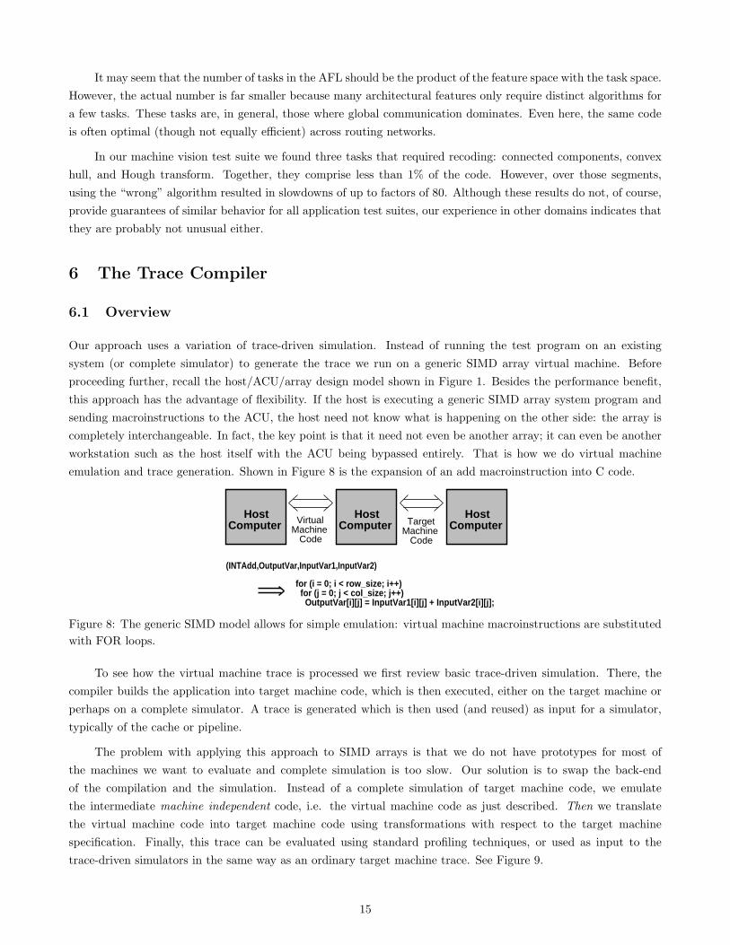
6.1 Overview
Our approach uses a variation of trace-driven simulation. Instead of running the test program on an existing
system (or complete simulator) to generate the trace we run on a generic SIMD array virtual machine. Before
proceeding further, recall the host/ACU/array design model shown in Figure 1. Besides the performance benefit,
this approach has the advantage of flexibility. If the host is executing a generic SIMD array system program and
sending macroinstructions to the ACU, the host need not know what is happening on the other side: the array is
completely interchangeable. In fact, the key point is that it need not even be another array; it can even be another
workstation such as the host itself with the ACU being bypassed entirely. That is how we do virtual machine
emulation and trace generation. Shown in Figure 8 is the expansion of an add macroinstruction into C code.
HostComputer
HostComputer Virtual
Machine Code
TargetMachine Code
(INTAdd,OutputVar,InputVar1,InputVar2)
HostComputer
for (i = 0; i < row_size; i++) for (j = 0; j < col_size; j++) OutputVar[i][j] = InputVar1[i][j] + InputVar2[i][j];
Figure 8: The generic SIMD model allows for simple emulation: virtual machine macroinstructions are substituted
with FOR loops.
To see how the virtual machine trace is processed we first review basic trace-driven simulation. There, the
compiler builds the application into target machine code, which is then executed, either on the target machine or
perhaps on a complete simulator. A trace is generated which is then used (and reused) as input for a simulator,
typically of the cache or pipeline.
The problem with applying this approach to SIMD arrays is that we do not have prototypes for most of
the machines we want to evaluate and complete simulation is too slow. Our solution is to swap the back-end
of the compilation and the simulation. Instead of a complete simulation of target machine code, we emulate
the intermediate machine independent code, i.e. the virtual machine code as just described. Then we translate
the virtual machine code into target machine code using transformations with respect to the target machine
specification. Finally, this trace can be evaluated using standard profiling techniques, or used as input to the
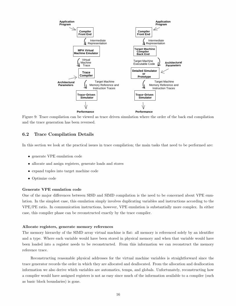
trace-driven simulators in the same way as an ordinary target machine trace. See Figure 9.
15
Architectural Parameters
ApplicationProgram
CompilerFront End
IntermediateRepresentation
Trace−Driven Simulator
Target MachineMemory Reference and
Instruction Traces
Performance
TraceCompiler
VirtualMachine Trace
MPA VirtualMachine Emulator
Target MachineExecutable Code
Detailed Simulator or Prototype
Target Machine Compiler Back End
IntermediateRepresentation
CompilerFront End
ApplicationProgram
Architectural Parameters
Trace−Driven Simulator
Target MachineMemory Reference and
Instruction Traces
Performance
Figure 9: Trace compilation can be viewed as trace driven simulation where the order of the back end compilation
and the trace generation has been reversed.
6.2 Trace Compilation Details
In this section we look at the practical issues in trace compilation; the main tasks that need to be performed are:
• generate VPE emulation code
• allocate and assign registers, generate loads and stores
• expand tuples into target machine code
• Optimize code
Generate VPE emulation code
One of the major differences between SISD and SIMD compilation is the need to be concerned about VPE emu-
lation. In the simplest case, this emulation simply involves duplicating variables and instructions according to the
VPE/PE ratio. In communication instructions, however, VPE emulation is substantially more complex. In either
case, this compiler phase can be reconstructed exactly by the trace compiler.
Allocate registers, generate memory references
The memory hierarchy of the SIMD array virtual machine is flat: all memory is referenced solely by an identifier
and a type. Where each variable would have been stored in physical memory and when that variable would have
been loaded into a register needs to be reconstructed. From this information we can reconstruct the memory
reference trace.
Reconstructing reasonable physical addresses for the virtual machine variables is straightforward since the
trace generator records the order in which they are allocated and deallocated. From the allocation and deallocation
information we also derive which variables are automatics, temps, and globals. Unfortunately, reconstructing how
a compiler would have assigned registers is not as easy since much of the information available to a compiler (such
as basic block boundaries) is gone.
16
A simple approach has proven quite successful: we treat the register set as if it were an explicitly managed
cache (which in some SIMD arrays, in fact, it still is). Determining which variables are currently in “register cache”
is then simply a case of applying standard cache analysis techniques to the physical memory reference trace.
How much does using dynamic assignment to reconstruct static assignment skew performance? Qualitatively
we know that in managing a cache, the cache controller can record when data has been used, information which is
not available at compile time. At trace evaluation time it is even a straightforward proposition to recreate perfect
register assignment (using optimal replacement). On the other hand, information known at compile time that aids
in static assignment has been lost.
In order to measure the effect quantitatively, we examine what matters most: the overall performance graphs.
Our approach is to bound the behavior of memory traffic that results from static register allocation with two
dynamic policies: one that should almost certainly do better than static allocation and one that is worse. On the
“better” side we use LRU, as it uses dynamic information about locality of references (the OPT results vary only
slightly). On the “worse” side we use a hybrid policy: we use the information about temps and automatics to
statically allocate the evaluation stack. The rest of the replacement is done randomly. Sample results are presented
in [19]. We found the differences to be surprisingly small, especially when it came to the critical result of curve
knee location and certainly adequate in determining the range of designs suitable for further study.
Optimize Code
Besides register assignment, there are several aspects to reconstructing back end code optimization.
• Optimizations carried out by the front end are still carried out there and do not need to be reconstructed.
• Address and index computations, where many optimizations at this level are commonly made, are a minor
component of most SIMD array programs: PE instructions are already operating on arrays in parallel.
• Much of the code generation is actually done in the ACU and so this behavior need not be reconstructed.
• Peephole optimization performs transformations such as dead code removal. The trace compiler includes a
pass that does this as well.
In our reconstruction of optimization, as in register assignment, we do not attempt to output exactly what
the target machine would have executed. For example, it would only be with great difficulty that we would be
able to determine from the trace the locations of basic block and procedure boundaries. As a consequence, we
are not always able to determine what optimizations a compiler cannot be assumed to be capable of carrying out.
However, because of the nature of the SIMD array programs, the fact that only back end optimization needs to be
addressed, and the way much of the final code generation gets done (by the ACU anyway), the criticality of this
fact is diminished. This is confirmed in our comparisons with real compiled code.
6.3 Performance
Three factors contribute to evaluator throughput when using trace compilation: i) the time needed to generate the
traces (virtual machine emulation), ii) the time needed to compile them and create the database entries, and iii)
the time needed to assimilate the data with respect to the machine templates and generate the reports. We have
found that the virtual machine emulation of typical image understanding applications takes from a few seconds to
a few minutes and from 30 to 487 times faster than on the CAAPP instruction-level simulator. A sample of these
results is shown in Table 6. The applications are described in [14]. The time needed to generate a complete set of
17
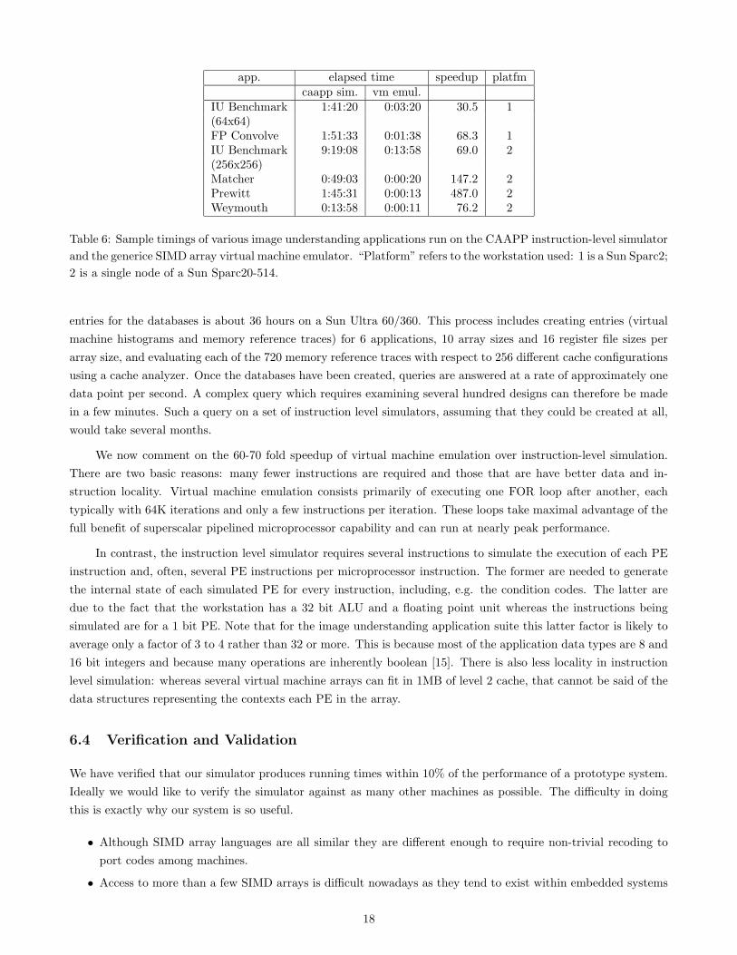
app. elapsed time speedup platfmcaapp sim. vm emul.
IU Benchmark 1:41:20 0:03:20 30.5 1(64x64)FP Convolve 1:51:33 0:01:38 68.3 1IU Benchmark 9:19:08 0:13:58 69.0 2(256x256)Matcher 0:49:03 0:00:20 147.2 2Prewitt 1:45:31 0:00:13 487.0 2Weymouth 0:13:58 0:00:11 76.2 2
Table 6: Sample timings of various image understanding applications run on the CAAPP instruction-level simulator
and the generice SIMD array virtual machine emulator. “Platform” refers to the workstation used: 1 is a Sun Sparc2;
2 is a single node of a Sun Sparc20-514.
entries for the databases is about 36 hours on a Sun Ultra 60/360. This process includes creating entries (virtual
machine histograms and memory reference traces) for 6 applications, 10 array sizes and 16 register file sizes per
array size, and evaluating each of the 720 memory reference traces with respect to 256 different cache configurations
using a cache analyzer. Once the databases have been created, queries are answered at a rate of approximately one
data point per second. A complex query which requires examining several hundred designs can therefore be made
in a few minutes. Such a query on a set of instruction level simulators, assuming that they could be created at all,
would take several months.
We now comment on the 60-70 fold speedup of virtual machine emulation over instruction-level simulation.
There are two basic reasons: many fewer instructions are required and those that are have better data and in-
struction locality. Virtual machine emulation consists primarily of executing one FOR loop after another, each
typically with 64K iterations and only a few instructions per iteration. These loops take maximal advantage of the
full benefit of superscalar pipelined microprocessor capability and can run at nearly peak performance.
In contrast, the instruction level simulator requires several instructions to simulate the execution of each PE
instruction and, often, several PE instructions per microprocessor instruction. The former are needed to generate
the internal state of each simulated PE for every instruction, including, e.g. the condition codes. The latter are
due to the fact that the workstation has a 32 bit ALU and a floating point unit whereas the instructions being
simulated are for a 1 bit PE. Note that for the image understanding application suite this latter factor is likely to
average only a factor of 3 to 4 rather than 32 or more. This is because most of the application data types are 8 and
16 bit integers and because many operations are inherently boolean [15]. There is also less locality in instruction
level simulation: whereas several virtual machine arrays can fit in 1MB of level 2 cache, that cannot be said of the
data structures representing the contexts each PE in the array.
6.4 Verification and Validation
We have verified that our simulator produces running times within 10% of the performance of a prototype system.
Ideally we would like to verify the simulator against as many other machines as possible. The difficulty in doing
this is exactly why our system is so useful.
• Although SIMD array languages are all similar they are different enough to require non-trivial recoding to
port codes among machines.
• Access to more than a few SIMD arrays is difficult nowadays as they tend to exist within embedded systems
18
or as coprocessors.
• Instruction-level simulators can be very accurate and it is possible to use them for verification. The problem
is that they present the same portability and availability issues as physical machines.
It is possible, however, to verify the simulator in a less direct but only slightly less compelling manner than
measuring with respect to real machines. The first point to note is that verifying an instruction-level SIMD
simulator is much more like verifying a SISD simulator than a MIMD one: models of both workload and machine
are entirely deterministic. Because of this, just implementing the specification correctly is sufficient, or, to put it
another way, validation is close to verification. For example, our instruction level simulator produces running times
within 1% of the measured prototype performance. The second point is that trace compilation adds only few places
where errors can be introduced, besides the user-introduced systematic kind such as mis-specifying the machine.
To review the major steps in trace compilation:
• The virtual machine code is generated by the same compiler front end that generates our SIMD array code.
• The virtual machine emulation that generates the trace outputs the same results as the SIMD array code.
• There is room for error in register assignment (and therefore the generation of loads and stores) as well as in
code optimization. However, because of the nature of SIMD arrays and SIMD array code, and because of the
shared front ends between target machine and virtual machine compilers, these errors are likely to be small.
• The tuple performance values in the target machine models represent the number of SIMD array cycles
executed. These actions on these cycles are the same as those that would be generated by an ACU (and are
precisely the same in the case of our machine).
The first two steps generate no errors. The third step can introduce an error, but we have already discussed why
this is likely to be tolerable. The fourth step introduces errors only due to user mis-specification of the target
machine.
A final point about the measured performance errors are that they are in the execution times, not in the
architectural recommendations. The recommendations suggested by the results described above would be the
same, even if the errors were much greater.
7 Hardware Generation and Analysis
7.1 Hardware Analyzer Function
The task of the hardware analyzer is to obtain area and timing of candidate designs. There are three issues: whether
information generated by synthesis tools offers sufficient information to provide accurate results, estimating timing
for large arrays, and the mechanism by which we parameterize and generate the designs.
Synopsys accuracy
Most preliminary industrial ASIC designs are evaluated by using the Synopsys timing and area reports so it should
be appropriate for the type of exploratory work we are doing here. Also, we (and most other creators of ASICs), use
standard cell technology libraries. This means that gate size and timing are known. The wiring is more problematic:
Synopsys uses statistical models to infer timing and area from fanout. The key to making these models valid is to
19

keep the wires short. This we do with the exception of the clock and instruction issue which, although critical, are
generally not part of preliminary design space exploration.
Estimating timing for large arrays
Synthesizing very large arrays is time consuming, memory intensive, and not necessary since most of the critical
paths for PE timing, and thus instruction execution, are short. We therefore generate 16x16 arrays to get the size
and timing of the PEs and the proportion of the area used for interPE wiring and the instruction bus.
HDL code generator
We now describe why we created a Verilog code generator rather than parameterized Verilog code: the key issues
are synthesizeability and various software engineering concerns. Although Verilog allows for modeling at a high level
by EDA standards, behavioral modeling comes at the cost of relinquished control when the design is synthesized.
In fact, Synopsys recommends that behavioral Verilog never be used for synthesis. Simply, it is often the case that
the only way to generate efficient hardware is to specify the logic in intricate detail.
Verilog has a crude macro capability and also supports conditional compiles, but neither of these was found
to be appropriate. For example a macro that selects bits from a generic 2D array might look something like
out[(width*(i*rows+j)+width-1):(width*(i*rows+j)]
rather than the preferred out[‘index(i,j)]. Conditional compiles, on the other hand, lead to code that is unreadable
and therefore unsupportable. Our solution is to create a generator that for each input specification outputs the
appropriate Verilog code. Some examples follow. When generating PEs:
• Computing the log of the register file depth to get the size of the decoder.
• The nearest neighbor logic conditionally includes a multiplexor depending on the NEWS datapath width.
• The design of the NEWS multiplexor depends on the NEWS width and ALU width.
• For the cases where NEWS width is less than the datapath width, the nearest neighbor register must be a
shift register.
When generating the array the problem is one of indexing.
• The I/O buses are named by the row number they feed. This requires an extra index.
• The I/O shift registers are named by the row number and column number of the PE they enter into or exit
from. This requires two indices.
• The interPE nearest neighbor wires also require two indices, one for the row and one for the column.
• When wiring up the PEs, the decision has to be made whether a PE is on an edge of the array or not and
set or clear the edge register accordingly.
That the logic is obviously trivial in C and not when using Verilog conditional compilation justifies our decision.
7.2 Hardware Analyzer Throughput and Sample Timings
The hardware analyzer throughput is dominated by the synthesis time. Components such as the register files,
ALUs, and multipliers have been presynthesized so array synthesis is comprised of creating a PE and using it and
the support circuitry to create an array. This can take a few hours per design.
20
Register File Size in BytesDatapath 16 32 64 128 256
1 1.92 2.26 2.42 2.55 2.822 2.09 2.20 2.43 2.63 2.944 2.43 2.51 2.79 2.85 3.098 2.57 2.74 2.75 2.94 3.3016 2.96 3.01 3.23 3.43 3.7932 3.22 3.33 3.36 3.63 3.96
Table 7: Sample cycle times of some PE designs in nanoseconds synthesized using the .35 micron ChipExpress
CX3000 gate array process library.
Some sample PE operating frequencies are shown in Table 7. Only register file and ALU are shown because
they comprise the critical path. That is because, in our hardware model, the multiplier, load/store, and floating
point are all explicitly removed from the critical path by making them multicycle operations when necessary. The
nearest neighbor network is never on the critical path.
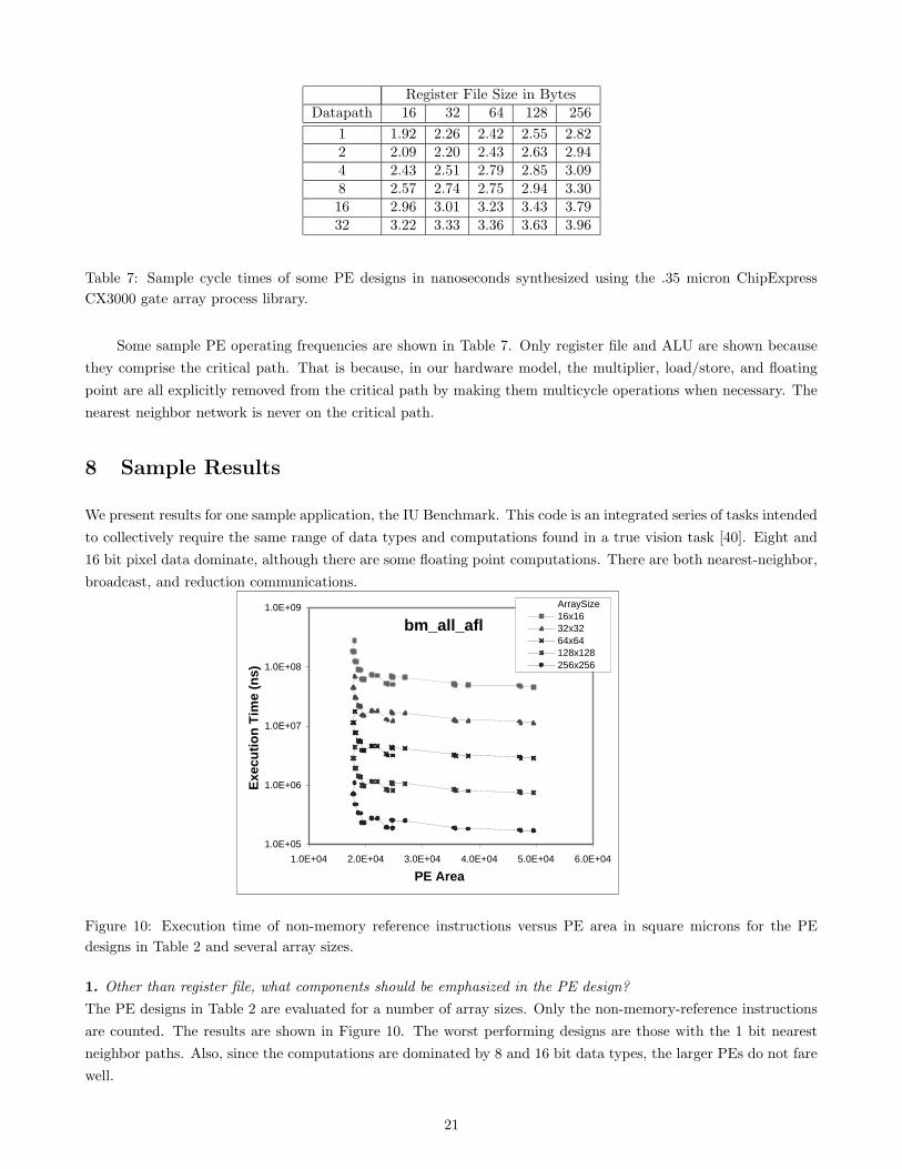
8 Sample Results
We present results for one sample application, the IU Benchmark. This code is an integrated series of tasks intended
to collectively require the same range of data types and computations found in a true vision task [40]. Eight and
16 bit pixel data dominate, although there are some floating point computations. There are both nearest-neighbor,
broadcast, and reduction communications.
bm_all_afl
1.0E+05
1.0E+06
1.0E+07
1.0E+08
1.0E+09
1.0E+04 2.0E+04 3.0E+04 4.0E+04 5.0E+04 6.0E+04
PE Area
Exe
cuti
on
Tim
e (n
s)
ArraySize16x1632x3264x64128x128256x256
Figure 10: Execution time of non-memory reference instructions versus PE area in square microns for the PE
designs in Table 2 and several array sizes.
1. Other than register file, what components should be emphasized in the PE design?
The PE designs in Table 2 are evaluated for a number of array sizes. Only the non-memory-reference instructions
are counted. The results are shown in Figure 10. The worst performing designs are those with the 1 bit nearest
neighbor paths. Also, since the computations are dominated by 8 and 16 bit data types, the larger PEs do not fare
well.
21
bm_all_afl
0.0E+00
2.0E+07
4.0E+07
6.0E+07
8.0E+07
1.0E+08
1.2E+08
1.4E+08
1.6E+08
1.8E+08
2.0E+08
16 66 116 166 216
Reg_File_Size
Exe
cuti
on
Tim
e ArraySize
16x16
32x32
64x64
128x128
256x256
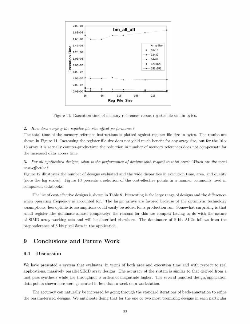
Figure 11: Execution time of memory references versus register file size in bytes.
2. How does varying the register file size affect performance?
The total time of the memory reference instructions is plotted against register file size in bytes. The results are
shown in Figure 11. Increasing the register file size does not yield much benefit for any array size, but for the 16 x
16 array it is actually counter-productive: the reduction in number of memory references does not compensate for
the increased data access time.
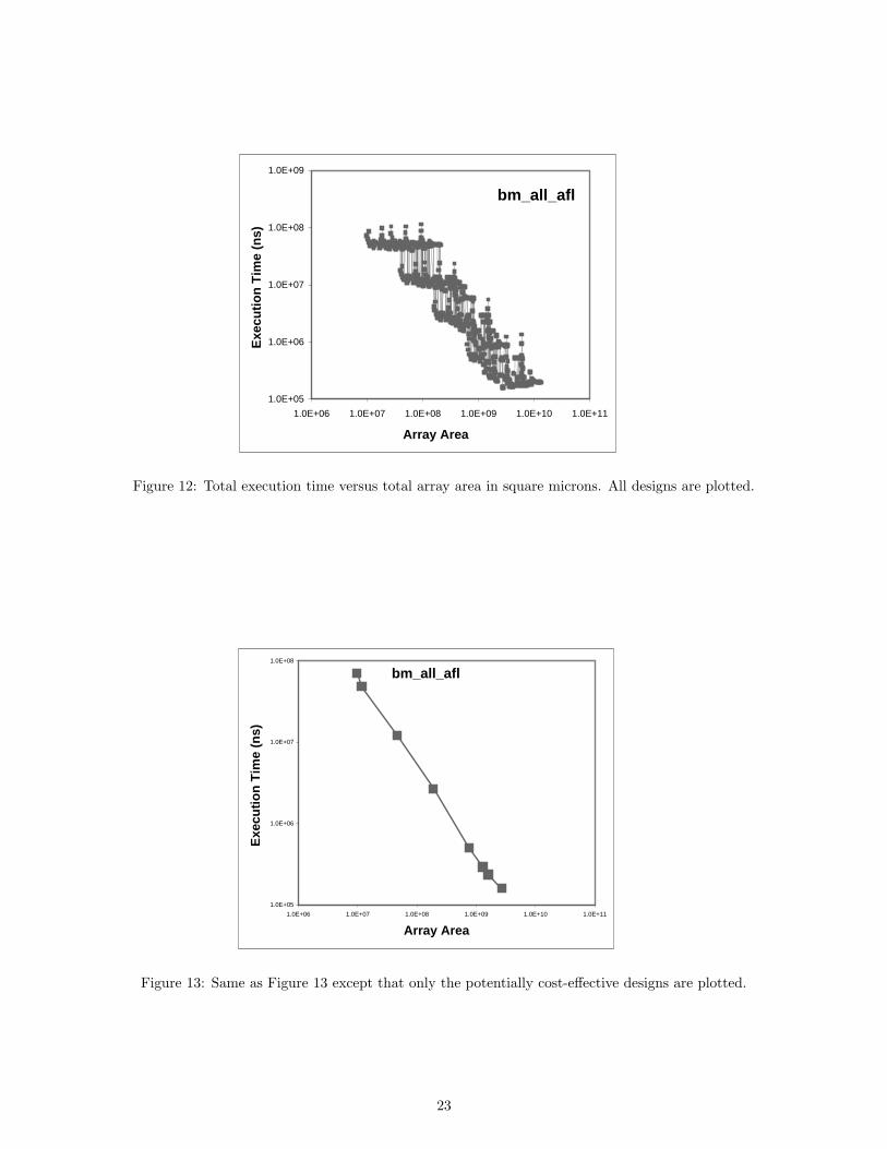
3. For all synthesized designs, what is the performance of designs with respect to total area? Which are the most
cost-effective?
Figure 12 illustrates the number of designs evaluated and the wide disparities in execution time, area, and quality
(note the log scales). Figure 13 presents a selection of the cost-effective points in a manner commonly used in
component databooks.
The list of cost-effective designs is shown in Table 8. Interesting is the large range of designs and the differences
when operating frequency is accounted for. The larger arrays are favored because of the optimistic technology
assumptions; less optimistic assumptions could easily be added for a production run. Somewhat surprising is that
small register files dominate almost completely: the reasons for this are complex having to do with the nature
of SIMD array working sets and will be described elsewhere. The dominance of 8 bit ALUs follows from the
preponderance of 8 bit pixel data in the application.
9 Conclusions and Future Work
9.1 Discussion
We have presented a system that evaluates, in terms of both area and execution time and with respect to real
applications, massively parallel SIMD array designs. The accuracy of the system is similar to that derived from a
first pass synthesis while the throughput is orders of magnitude higher. The several hundred design/application
data points shown here were generated in less than a week on a workstation.
The accuracy can naturally be increased by going through the standard iterations of back-annotation to refine
the parameterized designs. We anticipate doing that for the one or two most promising designs in each particular
22
bm_all_afl
1.0E+05
1.0E+06
1.0E+07
1.0E+08
1.0E+09
1.0E+06 1.0E+07 1.0E+08 1.0E+09 1.0E+10 1.0E+11
Array Area
Exe
cuti
on
Tim
e (n
s)
Figure 12: Total execution time versus total array area in square microns. All designs are plotted.
bm_all_afl
1.0E+05
1.0E+06
1.0E+07
1.0E+08
1.0E+06 1.0E+07 1.0E+08 1.0E+09 1.0E+10 1.0E+11
Array Area
Exe
cuti
on
Tim
e (n
s)
Figure 13: Same as Figure 13 except that only the potentially cost-effective designs are plotted.
23
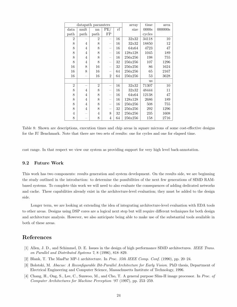
datapath paramters array time areadata mult nn PE/ rf size 0000s 000000spath path path FP cycles2 – 2 – 16 32x32 34118 108 4 8 – 16 32x32 18850 128 4 8 – 16 64x64 4723 478 4 8 – 16 128x128 1045 1898 4 8 – 16 256x256 198 7558 4 8 – 32 256x256 107 129616 8 16 – 32 256x256 86 162416 8 16 – 64 256x256 65 216716 – 16 2 64 256x256 53 3628
us2 – 2 – 16 32x32 71307 108 4 8 – 16 32x32 48444 118 4 8 – 16 64x64 12138 478 4 8 – 16 128x128 2686 1898 4 8 – 16 256x256 508 7558 4 8 – 32 256x256 292 12964 – 4 8 32 256x256 235 16088 – 8 4 64 256x256 158 2716
Table 8: Shown are descriptions, execution times and chip areas in square microns of some cost-effective designs
for the IU Benchmark. Note that there are two sets of results: one for cycles and one for elapsed time.
cost range. In that respect we view our system as providing support for very high level back-annotation.
9.2 Future Work
This work has two components: results generation and system development. On the results side, we are beginning
the study outlined in the introduction: to determine the possibilities of the next few generations of SIMD RAM-
based systems. To complete this work we will need to also evaluate the consequences of adding dedicated networks
and cache. These capabilities already exist in the architecture-level evaluation; they must be added to the design
side.
Longer term, we are looking at extending the idea of integrating architecture-level evaluation with EDA tools
to other areas. Designs using DSP cores are a logical next step but will require different techniques for both design
and architecture analysis. However, we also anticipate being able to make use of the substantial tools available in
both of these areas.
References
[1] Allen, J. D., and Schimmel, D. E. Issues in the design of high performance SIMD architectures. IEEE Trans.on Parallel and Distributed Systems 7, 8 (1996), 818–829.
[2] Blank, T. The MasPar MP-1 architecture. In Proc. 35th IEEE Comp. Conf. (1990), pp. 20–24.
[3] Bolotski, M. Abacus: A Reconfigurable Bit-Parallel Architecture for Early Vision. PhD thesis, Department ofElectrical Engineering and Computer Science, Massachusetts Institute of Technology, 1996.
[4] Chang, H., Ong, S., Lee, C., Sunwoo, M., and Cho, T. A general purpose Slim-II image processor. In Proc. ofComputer Architectures for Machine Perception ‘97 (1997), pp. 253–259.
24
[5] Dung, L.-R., and Madisetti, V. K. Conceptual prototyping of scalable embedded DSP systems. IEEE Designand Test of Computers 13, 3 (1996), 54–65.
[6] Elliot, D. G., Stumm, M., Snelgrove, W. M., Cojocaru, C., and McKenzie, R. Comutational RAM: Imple-menting processors in memory. IEEE Design and Test of Computers 16, 1 (1999), 32–41.
[7] Foster, C. C. Content Addressable Parallel Processors. Van Nostrand Reinhold Co., New York, NY, 1986.
[8] Fountain, T. J. CLIP4: a progress report. In Languages and Architectures for Image Processing, S. L. M. J.B. Duff, Ed. Academic Press, Boston, MA, 1981.
[9] Fujita, Y., Kyo, S., Yamashita, N., and Okazaki, S. A 10 GIPS SIMD processor for pc-based real-time visionapplications. In Proc. of Computer Architectures for Machine Perception (1997), pp. 22–32.
[10] Fujita, Y., Yamashita, N., and Okazaki, S. A 64 parallel integrated memory array processor and a 30 gipsreal-time vision system. In Proc. of Computer Architectures for Machine Perception (1995), pp. 242–249.
[11] Gargini, P., Glaze, J., and Williams, O. The semiconductor industry association roadmap. Solid StateTechnology 41, 73 (1998).
[12] Gealow, J. C., Herrmann, F. P., Hsu, L. T., and Sodini, C. G. System design for pixel parallel image processing.IEEE Transactions on Very Large Scale Integration (VLSI) Systems 4 (1996).
[13] Gokhale, M., Holmes, B., and Iobst, K. Processing in memory: The Terasys massively parallel PIM array.IEEE Computer 28, 4 (1995).
[14] Herbordt, M. C. The Evaluation of Massively Parallel Array Architectures. PhD thesis, Dept. of Comp. Sci.,U. of Mass. (also TR95-07), 1994.
[15] Herbordt, M. C., Anand, A., Kidwai, O., Sam, R., and Weems, C. C. Processor/memory/array size tradeoffsin the design of SIMD arrays for a spatially mapped workload. In Proc. of Computer Architectures for MachinePerception (1997), pp. 12–21.
[16] Herbordt, M. C., Corbett, J. C., Spalding, J., and Weems, C. C. Practical algorithms for online routing onfixed and reconfigurable meshes. J. Par. Dist. Comp. 20, 3 (1994), 341–356.
[17] Herbordt, M. C., Olin, K., and Le, H. Design trade-offs of low-cost multicomputer networks. In Proc. of the7th Symposium on the Frontiers of Massively Parallel Computation (1999), pp. 25–34.
[18] Herbordt, M. C., and Weems, C. C. An empirical study of datapath, memory hierarchy, and network inmassively parallel array architectures. In Proc. of the 1995 Int. Conf. on Computer Design (1995), pp. 546–551.
[19] Herbordt, M. C., and Weems, C. C. Experimental analysis of some SIMD array memory hierarchies. In Proc.of the 1995 Int. Conf. on Parallel Processing (1995), vol. 1: Architecture, pp. 210–214.
[20] Hunt, D. J. The ICL DAP and its application to image processing. In Languages and Architectures for ImageProcessing, S. L. M. J. B. Duff, Ed. Academic Press, London, 1981.
[21] Ikenaga, T., and Ogura, T. Cam2: A highly-parallel two-dimensional cellular automaton architecture. IEEETrans. on Computers C-47, 7 (1998), 788–801.
[22] Irwin, M. J., and Owens, R. M. A two-dimensional, distributed logic architecture. IEEE Trans. on ComputersC-40, 10 (1991), 1094–1101.
[23] Kim, Y., Noh, M.-J., Han, T.-D., Kim, S.-D., and Yang, S.-B. Memory-based processor array for artificialneural networks. In Proc. of the Int. Conf. on Neural Networks (1997), pp. 416–423.
[24] Komuro, T., Ishii, I., and Ishikawa, M. Vision chip architecture using general-purpose processing elements for1ms vision system. In Proc. of Computer Architectures for Machine Perception ‘97 (1997), pp. 276–279.
[25] Li, H., and Maresca, M. Polymorphic Torus Network. IEEE Trans. on Computers C-38, 9 (1989), 1345–1351.
[26] Little, J. J., Blelloch, G. E., and Cass, T. A. Algorithmic techniques for computer vision on a fine-grainedparallel machine. IEEE Trans. on Pattern Analysis and Machine Intelligence PAMI-11, 3 (1989), 244–257.
[27] MasPar Computer Corporation. The design of the MasPar MP-2: A cost effective massively parallel computer.Tech. rep., MasPar Computer Corportation, 1992.
[28] McConnell, R. Massively parallel simd computing on a single chip. In Proc. of the 11th HOT Chips Symposium(1999).
25
[29] McCormick, B. T. The Illinois Pattern Recognition Computer – ILLIAC III. IEEE Trans. on ElectronicComputers C-12, 12 (1963), 791–813.
[30] Miller, R., Kumar, V. K. P., Reisis, D., and Stout, Q. F. Parallel computations on reconfigurable meshes.IEEE Trans. on Computers C-42, 6 (1993), 678–692.
[31] Sima, D., Fountain, T., and Kacsuk, P. Advanced Computer Architectures: A Design Space Approach. Addison-Wesley, Harlow, England, 1997.
[32] Swarztrauber, P. N. Transposing arrays on multicomputers using de Bruijn sequences. Journal of Parallel andDistributed Computing 53 (1998), 63–77.
[33] Systems Performance Evaluation Cooperative. SPEC Newsletter: Benchmark Results. Waterside Associates,Freemont, CA, 1990.
[34] Thinking Machines Corporation. Connection Machine model: CM-2 technical summary. Tech. Rep. T.R.HA87-4, Thinking Machines Corporation, Cambridge, MA, 1987.
[35] Tomlinson, C. D. A Highly Parallel Image Processing Computer Architecture Suitable for Implementation inNanotechnology. PhD thesis, London University, Dept. of Physics and Astronomy, University College, 1997.
[36] Torrance, R., and et al. A 33GB/s 13.4Mb integrated graphics accelerator and frame buffer. In Proc. Intl.Solid-State Circuits Conf. (1998), pp. 340–341.
[37] Weems, C. C. Image Processing on a Content Addressable Array Parallel Processor. PhD thesis, U. of Mass.,Dept. of Comp. and Inf. Science, U. of Mass., Amherst, MA 01003, 1984.
[38] Weems, C. C., and Burrill, J. R. The Image Understanding Architecture and its programming environment.In Parallel Architectures and Algorithms for Image Understanding, V. Prasanna Kumar, Ed. Academic Press,Orlando, FL, 1991.
[39] Weems, C. C., Levitan, S. P., Hanson, A. R., Riseman, E. M., Nash, J. G., and Shu, D. B. The ImageUnderstanding Architecture. Int. Journal of Computer Vision 2, 3 (1989).
[40] Weems, C. C., Riseman, E. M., Hanson, A. R., and Rosenfeld, A. The DARPA image understanding benchmarkfor parallel computers. JPDC 11 (1991).
[41] Yates, R. B., Thackar, N. A., Evans, S. J., Walker, S. N., and Ivey, P. A. An array processor for generalpurpose digital image compression. Journal of Solid-State Circuits 30, 3 (1995), 244–250.
26