Embed Size (px)
Citation preview
A Texas Instruments Application Report
Bulletin MP702

Copyright 1977
By
Texas Instruments Incorporated
All Rights Reserved
PRINTED IN U.S.A.
Information contained in this publication is believed to be accurate and
reliable. However, responsibility is assumed neither for its use nor for any
infringement of patents or rights of others that may result from its use. No
license is granted by implication or otherwise under any patent or patent
right of Texas Instruments or others.

Section
I
II
III
TABLE OF CONTENTS
Page
INTRODUCTION . . . . . . . . . . . . . . . . . . . . . . . . . . . . . . . . . . 1
TMS 9900 ARCHITECTURE 2. 1 Registers ..... . 2.1.1 Workspace Pointer 2. 1.2 Workspace Registers 2.1.3 Program Counter 2.1.4 Status Register 2.2 Memory-to-Memory Operations 2.3 Bus Structures 2.4 Context Switching 2.5 Machine Cycles . 2.5.1 ALU Machine Cycles 2.5.2 Memory Read Machine Cycles 2.5.3 Memory Write Machine Cycles 2.5.4 CRU Output Machine Cycles . 2.5.5 CRU Input Machine Cycles .. 2.5.6 Instruction Execution Exam pIes 2.6 Machine Cycle Limits . . . . . . .
ME?v.10RY 3.1 Memory Organization 3.1.1 RESET Vector 3.1.2 Interrupt Vectors . 3.1.3 Software Trap Vectors 3.1.4 LOAD Vector ..... 3.1.5 Transfer Vectors Storage 3.2 Memory Control Signals 3.2.1 Memory Read Cycle 3.2.2 Memory Write Cycle
.3
.3
.4
.4 .5 .5 .5 .5 .6 .7 .7 .7 .7 .7
.7
.7
.8
11 11 11 11 12 12 13 13 13 13 13 3.2.3 Read/Write Control with DBIN
3.2.4 Slow Memory Control . . . . . . . . . . . . . . . . . . . . . . . . . . . .. 13 3.2.5 Wait State Control 3.2.6 Memory Access Time Calculation 3.3 Static MEMORY 3.3.1 Address .... 3.3.2 Control Signals 3.3.3 Loading . . . . 3.4 Dynamic Memory 3.4.1 Refresh ....
iii
15 17 18 19 19 19
20 20

Section
TABLE OF CONTENTS (Continued)
3.4.2 Refresh Modes 3.4.2. 1 Block Refresh 3.4.2.2 Cycle Stealing 3.4.2.3 Transparent Refresh 3.5 Buffered Memory .. 3.6 Memory Parity 3.7 Direct Memory Access 3.8 Memory Layout
IV INTERR UPTS 4.1 RESET 4.2 LOAD
V
4.3 Maskable Interrupts 4.3 .1 Interrupt Service 4.3.2 Interrupt Signals 4.3.3 Interrupt Masking 4.3.4 Interrupt Processing Example
INPUT/OUTPUT .... 5.1 Direct Memory Access 5.2 Memory Mapped I/O 5.3 Communication Register Unit (CRU) 5.3.1 CRU Interface ....... . 5.3.2 CRU Machine Cycles .... . 5.3.2.1 CRU Output Machine Cycles 5.3.2.2 CRU Input Machine Cycles 5.3.3 CRU Data Transfer .. 5.3.3.1 Single Bit Instructions 5.3.3.2 LDCR Instruction 5.3.3.3 STCR Instruction 5.3.4 CRU Interface lDgic 5.3.4.1 TTL Outputs 5.3.4.2 TTL Inputs ... 5.3.4.3 Expanding CRU I/O 5.4 CRU Paper Tape Reader Interface
Page
20 20 20 22 22 23 25 25
29
29
29
30 30 31 32 34
37 37 37 38 39 39 39 39 39 40 40 41
. 42 42 42 44 44 46 47 47
47
5.4.1 Operation .... 5.4.2 Software Control 5.5 TMS 9902 Interface 5.5.1 Operation . . . . 5.5.2 Software Routines ................................... 49
iv

TABLE OF CONTENTS (Continued)
Section
5.6 Software - UART 5.7 Burroughs SELF-SCAN Display Interface 5.8 Matrix Keyboard Interface
VI AUXILIARY SYSTEM FUNCTIONS 6.1 Unused Op Codes . . . . . . 6.1.1 Unused Op Code Detection 6.1.2 Unused Op Code Processing 6.2 Software Front Panel .... 6.2.1 System Configuration for Software Front Panel 6.2.2 Memory Requirements 6.2.3 Description of Operation ... 6.2.3.1 Entry Into Front-Panel Mode 6.2.3.2 Single Instruction Execution 6.2.3.3 Return to Run Mode
VII ELECTRICAL REQUIREMENTS 7.1 TMS 9900 Clock Generation 7.1.1 TIM 9904 Clock Generator 7.1.2 TTL Clock Generator ... 7.2 TMS 9900 Signal Interfacing 7.2.1 Switching Levels .... . 7.2.2 Loading ......... . 7.2.3 Recommended Interface Logic . 7.2.4 System Layout
VIII TMS 9980A/81 . 8.1 Architecture 8.2 Memory .. 8.3 Interrupts . 8.4 Input/Output 8.5 External Instructions 8.6 TMS 9980A/81 System Clock
IX TMS 9900 FAMILY SUPPORT DEVICES
APPENDIX A TMS 9900 FAMILY MACHINE CYCLES A.l General Description of Machine Cycles A.I.l ALU Cycle ............ .
v
Page
. 51 . 54
55/56
. " ...
57 57 57 57 57 58 59 60 60 60 62
t::'2 VJ
63 63 64 67 67 68 69 69
71 73 73 76 78 78 78
........... 85
89 89 89

Section
A.l.2 Memory Cycle A.1.3 CRU Cycle ..
TABLE OF CONTENTS (Concluded)
Page
89 89
A.2 TMS 9900 Machine Cycle Sequences 90 A.3 Terms and Definitions 90 A.4 Data Derivation Sequences .. 91 A.4.1 Workspace Register . . . . . 91 A.4.2 Workspace Register Indirect 91 A.4.3 Workspace Register Indirect Auto-Increment (Byte Operand) 91 A.4.4 Workspace Register Indirect Auto-Increment (Word Operand) 91 A.4.S Symbolic ........... 91 A.4.6 Indexed ........................... 92 A.S Instruction Execution Sequences . . . . . . . . . . . . . . . . 92 A.S.l A, AB, C, CB, S, SB, SOC, SOCB, SZC, SZCB, MOV, MOVB, COC, CZC, XOR 92 A.S.2 MPY (Multiply) 93 A.S.3 DIV (Divide) .................... 93 A.S.4 XOP ....................... 94 A.S.S CLR, SETO, INV, NEG, INC, INCT, DEC, DECT 9S A.S.6 ABS 9S A.S.7 X . 96 A.S.8 B . 96 A.S.9 BL 97 A.S.lO BLWP 97 A.S.ll LDCR 98 A.S.12 STCR 98 A.S.13 SBZ, SBO 99 A. S.14 TB 100 A.S.lS JEQ, JGT, JH, JHE, JL, JLE, JLT, JMP, JNC, JNE, JNO, JOC, JOP 100 A.S.16 SRA, SLA, SRL, SRC 100 A.S.17 AI, ANDI, ORI 101 A.S.18CI ., 101 A.S.19LI .. 102 A.S.20 LWPI 102 A.S.21 LIMI 102 A.S.22 STWP, STST 103 A.S.23 CKON, CKOF, LREX, RSET 103 A.S.241DLE ............ 103 A.6 Machine-Cycle Sequences in Response to External Stimuli 104 A.6.l RESET . 104 A.6.2 LOAD 104 A.6.3 Interrupts lOS
vi

liST OF ILLUSTRATIONS
Figure No.
1-1 TMS 9900 Microprocessor
2-1 TMS 9900 Architecture 2-2 TMS 9900 System Bus Structure 2-3 SBO Instruction Machine Cycles 2-4 STCR Instruction Machine Cycles 2-5 RTWP Instruction Machine Cycles 2-6 A Instruction Machine Cycles 2-7 Memory Cycle Pulse Generation 2-8 Memory Cycle Pulse Timing . .
3-1 TMS 9900 Dedicated Memory Addresses 3-2 Memory-Read Cycle Timing ...... . 3-3 Memory-Write Cycle Timing . . . . . . . 3-4 Read/Write Control Using MEMEN and DB IN 3-5 Memory-Read Cycle With One Wait State 3-6 Memory-Write Cycle With One \Vait State 3-7 Single Wait State for Slow Memory 3-8 Double Wait States for Slow Memory 3-9 Memory Access Timing Calculation 3-10 Memory Wait Time for Slow Memory 3-11 TMS 9900 Static Memory System . . 3-12 Cycle-Stealing Dynamic RAM Refresh for TMS 4051 3-13 Buffered Memory with Mixed PROM/ROM 3-14 Memory Parity Generator Checker 3-15 DMA Bus Control ..... 3-16 HOLD and HOLDA Timing
4-1 RESET Machine Cycles 4-2 RESET Generation 4-3 LOAD Machine Cycle Sequence 4-4 LOAD Generation ...... . 4-5 Interrupt Linkage ...... . 4-6 Interrupt Processing Machine Cycle Sequence 4-7 System With 15 External Interrupts ..... 4-8 Eight-Input Interrupt System With Synchronization 4-9 Single-Interrupt System ..... . 4-10 External Interrupt Clearing Routine 4-11 LIMI Instruction Routine .....
vii
Page
,., .L
.3
.6
.8
.8
.8
.8 9/10 9/10
12 14 15 15 16 16 17 17 17 18 19 21 23 24 26 26
29 30 30 31 32 33 33 34 35 35 36

LIST OF ILLUSTRATIONS (Continued)
Figure No.
5-1 TMS 9900 I/O Capability ..... 5-2 8-Bit Memory Mapped I/O Interface 5-3 CRU Output Machine Cycle Timing 5-4 CRU Control Strobe Generation 5-5 CRU Input Machine Cycle Timing . 5-6 TMS 9900 Single-Bit CRU Address Development 5-7 Multiple-Bit CRU Output 5-8 Example CRU Input Circuit 5-9 Multiple-Bit CRU Input 5-10 Latched CRU Interface 5-11 Multiplexer CRU Interface 5-12 8-Bit CRU Interface ... 5-13 16-Bit CRU Interface 5-14 Paper Tape Reader Interface 5-15 Paper Tape Reader Control Program 5-16 Software Configuration for Two Paper Tape Readers
with Common Control Program 5-1 7 TMS 9902 Interface . . . . . . 5-18 TMS 9902 Control Programs 5-19 Software UART CRU Interface 5-20 Software UART Control Program 5-21 Display Control Interface 5-22 Burrough's SELF-SCAN Display Control Program 5-23 64-Key Scanning Circuit ............ .
6-1 Illegal Op Code Detection Circuitry ..... . 6-2 System Configuration for Software Front Panel 6-3 Software Front Panel Memory Requirements 6-4 Front PaneLControl Circuitry '" 6-5 Single Instruction Execution Timing
7-1 TMS 9900 Typical Clock Timing 7-2 TIM 9904 Clock Generator 7-3 TMS 9900 Clock Generator .. 7-4 Timing Diagram for TMS 9900 Clock Generator 7-5 MOS Level Clock Drivers ..... 7-6 tpLH vs V OH Typical Output Levels 7-7 tpo vs Load Capacitance (Typical)
viii
Page
37 38 40 40 41 41 42 42 43 43 44 45 45 46 47
48 49 50 51
52-53 .. 54 55/56 55/56
58 59 60 61 62
64 65 66 67 67 68 69

LIST OF ILLUSTRATIONS (Concluded)
Figure No.
8-1 TMS 9980A/81 Microprocessor. . . . . . . . . 8-2 TMS 9980A/81 and TMS 9900 Configurations. 8-3 TMS 9980A/81 Memory Data Formats. 8-4 TMS 9980A/81 Memory Map .... 8-5 TMS 9980A/81 Memory Bus Timing . 8-6 Single Wait States For Slow Memory 8-7 Double Wait States For Slow Memory 8-8 TMS 9980A/81 HOLD Timing .... 8-9 TMS 9980A/81 Interrupt Interfaces . 8-10 TMS 9980A/81 Single-Bit CRU Address Development.
8-11 8-Bit CRU Interface ............. . 8-1 2 TMS 9980A/81 16-Bit Input/Output Interface. 8-13 External Instruction Decode Logic 8-14 Example TMS 9980Aj81 Clock Oscillator. .
9-1 TMS 9901 Programmable System Interface 9-2 TMS 9902 Asynchronous Communication Controller 9-3 TMS 9903 Synchronous Communication Controller
A-I ALU Cycle ............... . A-2 CRU Cycle ............... . A-3 TMS 9900 Memory Cycle (No Wait States) A-4 TMS 9980A/81 Memory Cycle (No Wait States)
ix
Page
71 72 73 74 75 76 76 77 79 80 81 82
83/84 83/84
.. 86 87
. 88
106 106 107 108

Table No.
Table 2-1 Table 2-2
Table 3-1
Table 4-1
liST OF TABLES
TMS 9900 Workspace Registers Machine Cycle Limits
TMS 9900 Compatible Memories
Interru pt Priority Codes
Page
.. 4
. 9/10
........ 12
............ 34
Table 5-1 Instructions Generating CPU Cycles ............................ 39
Table 6-1 Unused Op Codes
Table 7-1 Switch Levels ........ . Table 7-2 TMS 9900 Bipolar Support Circuits
Table 8-1 Interrupt Level Data Table 8-2 External Instruction Codes
x
....... 58
68 70
80 83/84
SECTION I
INTRODUCTION
This manual describes the general operation of the TMS 9900 family of devices, interfacing details, and examples of several hardware configurations. The TMS 9900 family are microprocessors and peripheral support devices, produced using N-channel silicon-gate MOS technology and large-scale integration to provide a high degree of functional density with minimum component count and board area requirements.
The TMS 9900 and the TMS 9980A/81 microprocessors are single-chip 16-bit central-processing units (CPU's) with the word size, instruction set, and addressing capabilities normally associated \-vith full minicomputers. Both single-chip CPU's are easily and economically implemented in small or large systems because of their simple, yet flexible, interfacing and architecture. The TMS 9900 utilizes a IS-bit address bus and a 16-bit data bus to address 32K words of memory space. Individual byte addressing is accomplished by means of a sixteenth address bit maintained internally within the TMS 9900 CPU. The TMS 9980A/81 possesses the same versatility as the TMS 9900, but is implemented with a 14-bit address bus and an 8-bit data bus to directly address 16K bytes of memory space. This combination of CPU;s gives the systems designer wide flexibility in the development of microprocessor systems.
Two members of the growing family of support devices for the TMS 9900 and TMS 9980A/81 are the TMS 9901 programmable systems interface and the TMS 9902 asynchronous communications controller. The TMS 9901 provides six dedicated interrupts, seven dedicated I/O ports, nine programmable I/O or interrupt ports, and an interval timer, and is easily stacked to provide additional interrupt and I/O capabilities.
The TMS 9902 provides complete control of an asynchronous-communications channel to include baud rate generation, timing, and data serialization and deserialization. The TMS 9902 also provides an interval timer and all necessary modem control signals.
Texas Instruments continues to introduce additional support circuits and development tools for the TMS 9900 family. One new support circuit, soon to be introduced, is the TMS 9903 synchronous communications controller, which will provide all hardware control of a synchronous communications channel, as well as assuming much of the control overhead from the CPU.
In the following discussions the reader is assumed to be familiar with the TMS 9900 family architecture and instruction set. Specific points not addressed here can be resolved by reference to the following publications, which contain detailed descriptions and specifications of device timing, signal sequences, interface requirements, and\instruction sets of the TMS 9900 family.
• TMS 9900 Microprocessor Data Manual

• TMS 9980Aj81 Microprocessor Data Manual
• TMS 9901 Programmable Systems Interface Data Manual
• TMS 9902 Asynchronous Communication Controller Data Manual
• 990 Computer Family System Handbook
• TMS 9900 Microprocessor Assembly Language Programmers' Guide
The following sections discuss the TMS 9900 family of microprocessors from the point of view of the TMS 9900. With certain exceptions this discussion also describes the operation of the TMS 9980Aj81.
Those features specific to the operation of the TMS 9980Aj81 are discussed in detail in Section 8.
The TMS 9900 microprocessor is illustrated in Figure 1-1.
I/O ~ INTERFACE
~
{ INTERRUPT INTERFACE
.~ SYSTEM CONTROL INTERFACE l
A0001100
CRUOUT
CRUCLK
CRUIN
INTREO
ICO·IC3
lAO
RESET
LOAD
POWER
----------..--+12V +SV -SV GND
TMS 9900 CPU
<pl <P2 <p3 <P4 \.. ./
CLOCK
Figure 1-1. TMS 9900 Microprocessor
2
(AO' A14)
(DO·D1S)
MEMORY MEMEN
INTERFACE
WE
DBIN
READY
WAIT
HOLD } DMA HOLDA INTERFACE

SECTION II
TMS 9900 ARCHITECTURE
The TMS 9900 has an advanced memory-to-memory architecture. The advantages of this architecture are best illustrated by comparison to other microprocessors currently available.
2.1 Registers
As shown in Figure 2-1, most microprocessors contain a set of registers internal to the device. This places restrictions on the number and size of internal registers dUe to limitations of LSI device size and density. These internal registers are used to contain high usage data because they may be accessed more efficiently and used more flexibly than memory. However, when more register storage is required than is available, register contents must be temporarily saved in memory. When a processor changes from one operation to another it is often desirable to save all internal register contents in memory so that the program controlling the new function may use all of the internal registers. Then, upon return to the original function, the
registers are reloaded from memory.
TMS aOaOA
CPU
REGISTERS
PC
~ ALU D I FLAGS n '"
PROGRAM AND DATA REGISTERS iN CPU PACKAGE
AOOOll0l
MEMORY
PROGRAM DATA
TI\1S 9900
PROGRAM AND DATA REGISTERS IN MEMORY
• NUMBER OF WORKSPACE REGISTERS LIMITED ONLY BY MEMORY SIZE
• PROVIDES FAST CONTEXT SWITCHING
Figure 2-1. TNiS 9900 Architecture
3
MEMORY
REGIS"! ERS PROGRMII
DA1A
'\

2.1.1 Workspace Pointer
The high usage data registers for the TMS 9900 are defined as blocks of memory called workspaces. The location of a workspace in memory is defined by a single internal register called the workspace pointer. The workspace pointer contains the memory word address of the first of sixteen consecutive memory words in the workspace, thus the processor has access to sixteen 16-bit registers. When a different set of registers is required, the program simply reloads the workspace pointer with the address of the new workspace, resulting in a significant reduction in processor overhead when a new set of registers is required. Also, the number of workspace registers is limited only by the amount of memory in the system.
2.1.2 Workspace Registers
The uses of the workspace registers are shown in Table 2-1. All 16 (WRO-WRlS) may be used for storage of addresses, temporary data, and accumulated results. WRI-WRlS may be used as index registers to specify a bias from a fixed-memory location to select an instruction operand. Register 0 may contain the number of bit positions an operand is shifted by the shift instructions (SLA, SRA, SRC, and SRL). WRII will contain the return address when the branch and link (BL) instruction is executed. Bits 3-14 of WR 12 contain the CRU base address for CRU instructions. WRI3-WRlS will contain the internal register values which are reloaded when the return to workspace (RTWP) instruction is executed.
TABLE 2-1. TMS 9900 WORKSPACE REGISTERS
MEMORY
ADDRESS
I WORKSPACE POINTER] Q WP + 00
WP+02
WP+04
WP+06
WP+08
WP+OA
WP+OC
WP+OE
WP + 10
WP + 12
WP + 14
WP + 16
WP + 18
WP + 1A
WP + 1C
WP + 1E
REGISTER
0
1
2
3
4
5
6
7
8
9
10
11
12
13
14
15
4
DATA
OR
ADDRESSES
REGISTER USE
INDEX
CAPABILITY
1
- OPTIONAL SHIFT
COUNT
- BL RETURN ADDRESS
- CRU BASE ADDRESS
-SAVEDWP
- SAVED PC
- SAVED ST

2.1.3 Program Counter
The function of the program counter of the TMS 9900 is identical to that of the program counter in other microprocessors in that the PC contains the memory address of the next instruction to be executed. As each instruction is executed, the PC is automatically updated. Except when instructions or operations are performed which directly affect the PC, it is simply incremented to the next consecutive memory-word address as each instruction is executed.
2.1. 4 Status Register
The status register of the TMS 9900 is similar to that of other microprocessors in that it contains flag bits which indicate results of the most recent arithmetic or logical operation performed. Additionally, the TMS 9900 contains a 4-bit interrupt mask in STI2-ST15 which defines the lowest-priority level interrupt which will be recognized by the microprocessor.
2.2 Memory-to-Memory Operations
The TMS 9900 instructions are not limited to workspace registers for efficient data storage. The two-address instructions permit operations to be performed on any word in memory by any other word in memory. For example, a single add (A) instruction can add any memory word to any other memory word in the total 32K word memory space. Many microprocessor architectures require a series of instructions in which memory contents are moved to registers, added, and returned to memory. The TMS 9900 architecture minimizes program storage requirements by reducing the number of instructions and also reduces program complexity and documentation requirements, resulting in both lower memory cost and lower development cost for a TMS 9900 system.
2.3 Bus Structures
The TMS 9900 has separate memory, I/O, and interrupt bus structures as shown in Figure 2-2. Each bus structure is optimized for its individual function. The memory bus efficiently handles the uniform width memory words which are transferred in parallel between the CPU and memory. The memory reference instructions operate on p~rallel data words or bytes, with additional masking instructions to isolate individual bits. The TMS 9900 has separate address, control, and data outputs and uses standard memories without external address latches. The TMS 9900 64-pin package is economical since the elimination of control or address multiplexing eliminates several external circuits and simplifies circuit layout. A complete discussion of memory interface to the TMS 9900 is contained in Section III.
TMS 9900 I/O uses the communication register unit (CRU) concept. Individual or multiple bits are transferred serially between the CPU and peripheral devices, thus the I/O instructions operate on individual bits and on variable length fields. While the TMS 9900 can also use memory mapped I/O, the CRU bus is normally more efficient and economical for I/O operations. Operation, interface, and applications examples for the CRU are contained in Section IV.
The TMS 9900 also has a separate interrupt bus structure that provides multiple vectored and prioritized interrupts without complex external vector generation or slow software polling procedures. Interrupt processing by the TMS 9900 is described in Section IV"
5

ADDRESS
""~--------r./
TMS 9900
I/O CPU
MEMORY 16 BIT
< I
l/\r-r-, -----t/~I /~---'/~I
CONTROL CONTROL ~ & DATA /'
~----------~ ~-4~~----~~:~~ __________________ ~_-_-_-~-_r~r----~ DATA
INTERRUPTS
A0001102 _____ ....IJr/
Figure 2-2. TMS 9900 System Bus Structure
2.4 Context Switching
When the TMS 9900 processes an interrupt, LOAD, or RESET, or executes an extended operation (XOP) or branch and load workspace pointer (BLWP) instruction, an operation called a context switch is automatically performed. The purpose of the context switch is twofold. First, the present internal registers (WP, PC, and ST) are stored in memory; second, new values for the WP and PC are loaded, thus setting up a different workspace and starting point for program execution.
The new values for the WP and PC are contained in dedicated memory locations which are described in Section 3.1. The BLWP instruction operand identifies the memory addresses which contain the new WP and PC values. The actual sequence in which the context switch is performed is as follows:
• The new WP is loaded into the CPU;
• The old ST is stored in WR1S of the new workspace;
• The old PC is stored in WR14 of the new workspace;
• The old WP is stored in WR13 of the new workspace;
• The new PC is loaded into the CPU and instruction execution begins at that point.
6

When the new program has completed execution, return to the originai context is performed by execution of the return workspace pointer (RTWP) instruction, which causes the values contained in WR 13-WR 14 to be reloaded into the internal registers.
2.5 Machine Cycles
Each operation performed by the TMS 9900 consists of a sequence of machine cycles. In each machine cycle the processor performs a data transfer with memory or the CRU and/or an arithmetic or logical operation internally with the ALU. A detailed discussion of the machine cycles for all instructions is contained in Appendix A.
2.5.1 AL U Machine Cycles
Each ALU machine cycle is two clock cycles long. In an ALU cycle no external data transfer occurs, but the ALU performs an arithmetic or logical operation on two operands contained internally.
2.5.2 Memory Read Machine Cycles
The function of the memory-read cycle is to transfer a word of data contained in memory to the processor. An ALU operation may be performed during a memory-read cycle. Memory-read cycles are a minimum of two clock cycles long. If wait states are inserted to allow access to slow memories, the length of the memory-read cycle is extended.
2.5.3 Memory Write Machine Cycles
The memory-write cycle is identical to the memory-read cycle, except that data is written to rather than read from memory.
2.5.4 CR U Output Machine Cycles
Each CR U output machine cycle is two clock cyles long. In addition to outputting a bit of CRU data, an ALU operation may also be performed internally.
2.5.5 CR U Input Machine Cycles
The CRU input cycle is identical to the CRU output cycle, except that one bit of data is input rather than output.
2.5.6 Instruction Execution Examples
Examples of how sequences of machine cycles are used to execute instructions are illustrated in Figures 2-3 to 2-6. Note that the first machine cycle of each instruction is always a memory-read cycle in which the instruction is fetched, and the second is always an ALU cycle.
7

2.6 Machine Cycle Limits
Table 2-2 lists information which will be useful for system design. The maximum number of consecutive memory-read cycles is used to calculate the maximum latency for the TMS 9900 to enter the hold state, since the hold state is only entered from ALU, CRU input, or CRU output machine cycles. The minimum frequency of consecutive memory jnon-memory cycle sequences occurs when the DIV instruction is executed. This number is used to ensure that the refresh rate meets specifications when the transparent-refresh mode described in paragraph 3.4.2.3 is used, since memory is refreshed in this mode each time an ALU or CRU cycle follows a memory cycle. Figure 2-7 shows the logic to generate a pulse for each memory access cycle, including consecutive cycles shown in Figure 2-8.
SSO OUTSIT
CYCLE TYPE FUNCTION
1 Memory Read I nstruction Fetch
2 ALU Decode Op Code
3 ALU Calculate Address of WR 12
4 Memory Read Fetch (WR 12)
5 ALU Calculate CRU Address
6 CRU Output Output Bit, Increment PC
A0001103
Figure 2-3. SBO Instruction Machine Cycles
STCR RO,5
CYCLE TYPE FUNCTION
1 Memory Read I nstruction Fetch
2 ALU Decode Op Code
3 Memory Read Fetch (WRO)
4 ALU Calculate Address of WR 12
5 Memory Read Fetch (WR 12)
6 ALU Set Up
7 ALU Set Up
8-12 CRU Input Transfer 5 Bits
13 ALU Set Up
14 ALU Set Up
15-17 ALU Zero Filling
18 ALU Parity Generation
19 ALU Load WRO Address in MA
20 ALU~ Byte Positioning
21 Memory Write Store Data in WRO,
I ncrement PC AOOOll04
Figure 2-4. STCR Instruction Machine Cycles
8
CYCLE
1
2
3
4
5
6
7
A0001105
RTWP
TYPE
Memory Read
ALU
ALU
Memory Read
Memory Read
Memory Read
ALU
FUNCTION
I nstruction Fetch
Decode Opcode
Calculate Address of WR 15
Restore Status from WR 15
Restore PC from WR 14
Restore WP from WR 13
Load PC into MA
Figure 2-5. RTWP Instruction Machine Cycles
A *R1,R2
CYCLE TYPE FUNCTION
1 Memory Read I nstruction Fetch
2 ALU Decode Opcode
3 Memory Read Fetch (WR 1)
4 ALU Set Up
5 Memory Read Fetch ((WR1))
6 ALU Set Up
7 Memory Read Fetch (WR2)
8 ALU Addition
9 Memory Write Store Result in WR2,
Increment PC
A0001106
Figure 2-6. A Instruction Machine Cycles

ct>4TTL
MEMEN
READY
WAIT
TABLE 2-2. MACHINE CYCLE LIMITS MINIMUM MAXIMUM
Consecutive Memory Read Cycles 3
Consecutive Memory Write Cycles
Consecutive ALU Cycles 51
Consecutive CRU Cycles 16
Fisqusncy of Consecutive 5 pairs
memory/non-memory cycle {64 machine
pairs {used for transparent cycles during
refresh} DIV.l
VCC
MEMEN 1-----1 J Qt---- MEMCY
1ATTL
WAIT .......... ---1 K Q 1----_
A0001107 Figure 2-7. Memory Cycle Pulse Generation
~~ __________________ ~x~ _______________________________ ;-
,'-____ ----1
------------------------------------------~I \~-------
MEMCY ____ ----011 \ _____ .....J! \_-----AOOOl187
Figure 2-8. Memory Cycle Pulse Timing
9/10


SECTION III
MEMORY
The TMS 9900 workspace organization uses the system memory for register files in addition to program
and data storage. The TMS 9900 is easily interfaced to any of the standard types of semiconductor memory
devices. Texas Instruments provides masked ROMs, field-programmable ROMs (PROMs), and erasable PROMs (EPROMs) for non-volatile program and data storage. RAMs are available in sizes from a 64 x 8
static RAM to the 16K dynamic RAMs for use as temporary program and data storage. TMS 9900
compatible memory devices are listed in Table 3-1.
3.1 Memory Organization
The TMS 9900 instructions build a l6-bit address word which describes a 64K x 8 bit address space. The least-significant address bit is used internally by the CPU to select the even or odd byte, and the other 15
address bits are passed to external memory to describe a 32K x 16 bit address space. Although 32K words are the most locations that the CPU can directly access, additional memory can be accessed using address
bank switches or address mapping.
The advanced architecture of the TMS 9900 uses part of the ex ternal memory space for workspace register files and for transfer vector storage. For maximum design flexibility, only the locations of the transfer vectors are restricted. A memory map for the TMS 9900 is shown in Figure 3-1. The transfer vectors are the
ne\v WP and PC for the context switches described in Section 2.4.
3.1.1 RESET Vector
The first two memory words are reserved for storage of the RESET vector. The RESET vector is used to
load the new WP and PC whenever the CPU RESET signal occurs. The first word contains the new WP,
which is the starting address of the RESET workspace. The second word contains the new PC, which is the
starting address of the RESET service routine.
3.1.2 Interrupt Vectors
The next thirty memory words, 0004 16 through 003E 1 6 are reserved for storage of the interrupt transfer
vectors for levels 1 through 15. Each interrupt level uses a word for the workspace pointer (\VP) and a word
for the starting address of the service routine (PC). If an interrupt level is not used within a system, then the
corresponding two memory words can be used for program or data storage.
11

TABLE 3-l. TMS 9900 COMPATIBLE MEMORIES
Device Organization Package
Dynamic RAMs TMS 4030 4096X1 22
TMS 4050 4096X1 18
TMS 4051 4096X1 18
TMS 4060 4096X1 22
TMS 4070 16384X1 16
Static RAMs (NMOS)
TMS 4033 1024X1 16
TMS 4036-2 64X8 20
TMS 4039-2 256X4 22
TMS 4042-2 256X4 18
TMS 4043-2 256X4 16
ROMs (NMOS)
TMS 4700 1024X8 24
TMS 4800 2048X8 24
PROMs (TTL)
SN 74S287 256X4 16
SN 74S471 256X8 20
SN 74S472 512X8 20
SN 74S474 512X8 24
EPROMs (NMOS)
TMS 2708 1024X8 24
TMS 2716 2048X8 24
3.1. 3 Software Trap Vectors
The next thirty-two memory words, 00040 1 6
through 007E 1 6, are used for extended-operation software trap vectors. When the CPU executes one of the 16 extended operations (XOPs), the pro-
AREA DEFINITION
INTERRUPT VECTORS
XOPSOFTWARE TRAP VECTORS
GENERAL MEMORY FOR
PROGRAM,DATA,AND
WORKSPACE REGISTERS
LOAD SIGNAL VECTOR
AOOOll08
MEMORY
ADDRESS16
0000
0002
0004
0006
oo3C
oo3E
0040
0042
oo7C
oo7E
0080
.iI-
....
MEMORY CONTEN r 15
WP RESET FUNCITON
PC RESET FUNCTION
WP LEVel 1 INTERRUPT
PC LEVEL ~ INTERRUPT
.. ~ WP LEVEL 15 INTERRUPT
PC LEVEL 15 INTERRUPT
WP XOPO
PC XOPO
.. ~ WP XOP 15
PC XOP 15
--GENERAL M-EMORY AREA
MAY BE ANY
COMBINATION OF
PROGRAM SPACE
OR WORKSPACE
--
{
FFFC
FFFE
WP LOAD FUNCTION
PC LOAD FUNCTION
Figure 3-1. TMS 9900 Dedicated Memory Addresses
gram traps through the corresponding vector. Two words are reserved for each trap vector, with one word for the WP and one word for the PC. If an XOP instruction is not used, the corresponding vector words can be used for program or data storage.
3.1.4 LOAD Vecfur
The last two memory words FFFC I 6 and FFFEI 6 are reserved for the LOAD vector, with one word for the WP and one word for the PC. the LOAD vector is used whenever the CPU LOAD signal is active (low).
12

3.1.5 Transfer Vectors Storage
The transfer vectors can be stored either in ROM or RAM, but the reset vector should be in non-volatile memory to ensure proper system start-up. The restart routine should initialize any vector which is in RAM. The program can then manipulate the RAM-based vectors to alter workspace assignments or service routine entry points, while ROM-based vectors are fixed and cannot be altered.
3.2 Memory Control Signals
The TMS 9900 uses three signals to control the use of the data bus and address bus during memory read or write cycles. Memory enable (MEMEN) is active (low) during all memory cycles.
Data bus in (DBIN) is active (high) during memory read cycles and indicates that the CPU has disabled the output data buffers.
Write enable (WE) is active (low) during memory write cycles and has timing compatible with the read/write (R/vV) control signal for many standard RAMs.
3.2.1 Memory Read Cycle
Figure 3-2 illustrates the timing for a memory read machine cycle with no wait states. At the beginning of the machine cycle, MEMEN and DBIN become active and the valid address is output on AO-A14. DO-D 15 output drivers are disabled to avoid conflicts with input data. WE remains high for the entire machine cycle. The READY input is sampled on </> I of clock cycle I, and must be high if no wait states are desired. Data is sampled on </> I of clock cycle 2, and set-up and hold timing requirements must be observed. A memory-read cycle is never followed by a memory-write cycle, and DO-DI5 output drivers remain disabled for at least one additional clock cycle.
3.2.2 Memory Write Cycle
Figure 3-3 illustrates the timing for a memory write machine cycle with no wait states. MEMEN becomes active, and valid address and data are output at the beginning of the machine cycle. DBIN remains inactive for the complete cycle. WE goes low on </> I of clock cycle I and goes high on </> I of clock cycle 2, meeting the address and data set-up and hold timing requirements for the static RAMs listed in Table 3-1. For no wait states, READY must be high during </> 1 of clock cycle 1.
3.2.3 Read/Write Control with DBIN
In some memory systems, particularly with dynamic RAMs, it may be desirable to have READ and WRITE control signals active during the full memory cycle. Figure 3-4 shows ho\-\' the \VRITE signal can be generated, since any memory cycle (MEMEN = 0) in which DB IN = 0 is a memory-write cycle.
3.2.4 Slow Memory Control
Although most memories operate with the TMS 9900 at the full system speed, some memories cannot properly respond within the minimum access time determined by the system clock. The system clock could
13

~ CLOCK CYCLE 1 ---i .. ~li-'II"l--- CLOCK CYCLE 2 ~ 1/11 r-------1 I I .l~ __ ---'
I I I
rJ>2 ~ ________ ~r__l~ ________ ~
I ~ y~-------_____ I~ __________________ ~ ________________ __JI
DBIN ~----~~----------------~------------------~I ---Y ~'---___ -
I I I I
I I I I I I
AO - A14 -~----______________ V_A_L_I_D_A~D-D-R-E-~---------------J)(~------------------I I
DO - 015 =X INPUT MODE 'tll-i I I ------------------~i------------~~~~,~-----------------
INPUT MODE
! I
READY
WAIT
I I I I
A0001109
Figure 3-2. Memory-Read Cycle Timing
be slowed down in order to lengthen the access time but the system through-put would be adversely affected since non-memory and other memory reference cycles would be unnecessarily longer. The READY and WAIT signals are used instead to synchronize the CPU with slow memories. The timing for memory-read and memory-write cycles with wait states is shown in Figures 3-5 and 3-6.
The READY input is tested on ¢ 1 of clock cycle 1 of memory-read and memory-write cycles. If READY = 1, no wait states are used and the data transfer is completed on the next clock cycle. If READY = 0, the processor enters the wait state on the next clock cycle and all memory control, address, and data signals maintain their current levels. The WAIT output goes high on ¢3 to indicate that a wait state has been entered. While in the wait state, the processor continues to sample READY on ¢ 1, and remains in the wait state until RE,A,"DY = 1. 'When READY = 1 the processor progresses to clock cycle 2 and the data transfer is completed. WAIT goes low on ¢3. It is important to note that READY is only tested during ¢ 1 of clock cycle I of memory-read and memory-write cycles and wait states, and the specified set-up and hold timing requirements must be met; at any other time the READY input may assume any value. The effect of inserting wait states into memory access cycles is to extend the minimum allowable access time by one clock period for each wait state.
14

¢1
1>2
<1>3
MEMEN
OBIN
WE
AO-A14
00-015
READY
WAIT
AOOOlll0
MEMEN t---.....
I I
1~~~----CLOCKCYCLE1----~~~:4~----CLOCKCYCLE2----~·~1
I
I I
\ y
i \ I ~~----------~/ I I
I ------------------~~-------------------X----~ I
~ ~----------------------~I----------------------~~-----I I I
I I I I I
I I I I
Figure 3-3. Memory-''''rite Cycle Timing
3.2.5 Wait State Control
OBI N '---+---4a----------READ
Figure 3-7 illustrates the connection of the WAIT output to the READY input to generate one wait state for a selected memory segment. The address decode circuity generates an active low signal (SLOMEM = 0) whenever the slow memory is addressed. For example, if memory addresses 800016 -FFFEI 6 select slow memory, SLOMEM = TMS 9900
AOOOllll
t-----WRITE
Figure 3-4. Read/Write Control Using MEMEN and DBIN
15
AO. If one wait state is required for all memory,
WAIT may be connected directly to READY, causing one wait state to be generated on each memory-read or memory-write machine cycle. Referring again to Figures 3-5 and 3-6, note that the WAIT output satisfies all of the timing

~CLOCKCYCLE 1--I"~I"""I---WAITSTATE "'1" CLOCKCYCLE2~
II II !I~----II~--~II I I I I
¢1
¢2 ~ ~ n ____ n~~ ¢3 __ ~I1 ___ ~_n II 11 ___ _
I
----: ----_II~~----~II~~----~II~--------~ 1 I
~~----------------~----------y~~--~-----------I 1 II~----------------------~------------~~----------------f 1\ _______ _ DurN
I
WE I i I I
AO·A ~4 .==J( ________ ...... __ V_A_L_ID_A_D_D_R_E_S_S_--,r--_______ ~~,---------
I I ---v VALID I DO-D15 .---fi INPUT MODE DAl A _
I ----------~------------~---------~--~~~---------------INPUT MODE
I
READY xxXXXXXXXXXXXl RXXXXXXXXJ WAIT ---------------------/ \_--------~-----------AOOOll12
<1>1
cp2
<P3
cp4
MEMEN
DBIN
WE
AO-A14
00015
READY
WAIT
AOOOl113
Figure 3-5. Memory-Read Cycle With One Wait State
~CLOCK CYCLE 1 - ..... 4---WAIT STATE-_.-+4--CLOCK CYCLE 2~
n ~ ________ r__l _________ ~r-l _________ _
n ~ _______ n 11 ____ __ I 1 __________________________________ ~V--~
1
I \ --~---------------------/ I
I I
~ -------------------------------V--VALID ADDRESS ~
I ----------------V-A-LI-O-W-R-IT-E-O-A-T-A------------------vc::=
I
~ XO<XXXXXXXXXXX> IXXXXXXXXXJ
----------------~~/ \_------~-Figure 3-6. Memory-Write Cycle With One Wait State
16

ADDRE$I ~I ADDRESS DECODE
READY '-----_--' TMS 9900 ~~L_O_ME_M_~
WAITt---------l
! A0001114
Figure 3-7. Single Wait State for Slow Memory
ADDRESSi J------------1 ... /
TMS 9900 READY 1---0
WAIT I------f
ADDRESS DECODE
requirements for the READY input for a single wait state. The address decode signal is active only when a particular set of memory locations has been addressed. Figure 3-8 illustrates the generation of two wait states for selected memory by simply delaying propagation of the WAIT output to the READY input one clock cycle with aD-type flip-flop. The rising edge of ¢ 2TTL is assumed to be coincident with the falling edge of the ¢ 2 clock input to the TMS 9900.
3.2.6 Memory Access Time Calculation
Maximum allowable memory access time for the TMS 9900 can be determined with the aid of Figure 3-9. Memory control and address signals are output on ¢2 of clock cycle I, and are stable 20 ns (tpLH, tpHL) afterwards. Data from memory must be valid 40 ns (tsu) before the leading edge of ¢ I during clock cycle 2. Therefore, memory access
A0001115 time may be expressed by the equation:
Figure 3-8. Double \Vait States for Slow Memory
~ CLOCK CYCLE 1 -I· WAIT STATE(S) -I. CLOCK CYCLE 2----+1
I .. ~! .. 1 O.75tcy~ I
t_ .. n·t,." .,. I
I -.. y I -, I
rt11 <:>1 J\ I 1\ 1 ,rf\ I I I
1
!f\ ;f\ 0 tr ~ ~ :0 1)2 1J I
I I I I 1
1\ 1
ILff I /\ I I I 03 I I I I 1
I I )~
I r1\ I
1>4 1\ I I 1 I
~ ~PHL.tpLH I I I I I I I 1
MEMEN ~ 1 I v= ( ( 1 I , J I I
AO-A14 X VALID ~ ~ADDRESS : : X= 1: f f 1 I
oBIN I f'= I ~ ~i
tsu-+-j I t-+th
00-015 f : I VALID rt-I ,I ... tacc ~I
AOOOll16
Figure 3-9. .Mel110ry Access Timing Calculation
17

where n equals the number of wait states in the memory-read cycle. Assigning worst-case specified values for tpLH (20 ns), tr (12 ns), and tsu (40 ns), and assuming 3 MHz operation:
(l.75 + n) tacc ~ 0.003 - 72 ns
Access time is further reduced by address decoding, control signal gating, and address and data bus buffering, when used. The graph in Figure 3-10 illustrates the above equation for varying nand tcy in an unbuffered memory system. Thus, for a known access time for a given device, the number of required wait states can be determined.
For example, a TMS 4042-2 RAM has a 450 nanosecond access time and does not require any wait states. A TMS 4042 has a 1000 nanosecond access time and requires two wait states. Propagation delays caused by address or data buffers should be added to the nominal device access time in order to determine the effective access time.
CLOCK PERIOD (ns)
800
700
600
500
tcy
400
300
200
100
200
AOOOll17
3.3 Static Memory
NO WAIT STATES
400 600
tPHL = 20 ns tsu = 40 ns tr = 12 ns
800
tacc
1000
ONE WAIT STATE
1200 1400
Figure 3-10. Memory Wait Time for Slow Memory
ACCESS TIME (ns)
Static RAMs and PROMs are easily interfaced to the TMS 9900. A TMS 9900 memory system using the TMS 4042-2 256 X 4 static RAM and the TMS 2708 lK X 8 EPROM is shown in Figure 3-11.
18

C'UI ~~." [>~I~I==n~1----1 ~l>---I ~ll~~=~k A~14 < < CE1 A:~ Cs A~: Cs A~: ~I
TMS 4042-2 TMS 2708 TMS 2708
TMS:;, I----------+---+--+-------+-+--~____+__I_--~/~-----.J,~ ill 0. o~. !
I .E:~~I d>~----+--~ I AOOQll18 Figure 3-11. TMS 9900 Static Memory System
3.3.1 Address
The most-significant address bit, AO, is used to select either the EPROMs or the RAMs during memory cycles. When AO is low, the EPROMs are selected, and when AO is high, the RAMs are selected. Address lines A 1 through A4 are not used since the full address space of the TMS 9900 is not required in the example. The lower address bits select internal RAM or EPROM cells. Other memory systems can fully decode the address word for maximum memory expansion.
3.3.2 Control Signals
Since DBIN is also used to select the EPROMs during memory-write cycles, the EPROMs cannot inadvertently be selected and placed into output mode while the CPU is also in the output mode on the data bus. MEMEN is used to select the RAMs during either read or write cycles, and WE is used to select the read/write mode. DBIN is also used to control the RAM output bus drivers.
The TMS 9900 outputs WE three clock phases after the address, data, and MEMEN are output. As a result, the address, data, and enable-hold times are easily met. WE is enabled for one clock cycle and satisfies the minimum write pulse width requirement of 300 nanoseconds. Finally, WE is disabled one clock phase before the address, data, and other control signals and meets the TMS 4042-2, 50-nanosecond minimum data and address hold time.
3.3.3 Loading
The loads on the CPU and memory outputs are well below the maximum rated loads. As a result no buffering is required for the memory system in Figure 3-11. The TMS 4042-2 and the TMS 2708 access times are low enough to eliminate the need for wait states, and the CPU READY input is connected to
VCC'
The minimum high-level input voltage of the TMS 2708 is 3 volts while the maximum high-output voltage for the TMS 9900 is 2.4 volts at the maximum specified loading. As described in Section 7.2.1, the TMS 9900 output voltage exceeds 3 volts and pull-up resistors are not needed for the system in Figure 3-11. The loads on the CPU and memory outputs are well below the maximum rated load and thus do not require buffering of the address or data lines.
19

There are many other Texas Instruments static memories compatible with the TMS 9900 as shown in Table 3-1. The memory devices in the table do not require wait states when used with the TMS 9900 at 3 MHz.
3.4 Dynamic Memory
Memory applications requiring large bit storage can use 4K or 16K dynamic memories for low cost, low power consumption, and high bit density. TMS 9900 systems requiring 4K words or more of RAM, can economically use the 4096-bit TMS 4051, the 16,384-bit TMS 4070, or any of the other dynamic RAMs shown in Table 3-1.
3.4.1 Refresh
The dynamic RAMs must be refreshed periodically to avoid the loss of stored data. The RAM data cells are organized into a matrix of rows and columns with on-chip gating to select the addressed bit. Refresh of the 4K RAM cell matrix is accomplished by performing a memory cycle of each of the 64 row addresses every 2 milliseconds or less. The 16K RAM has 128 row addresses. Performing a memory cycle at any cell on a row refreshes all cells in the row, thus allowing the use of arbitrary column address during refresh.
3.4.2 Refresh Modes
There are several dynamic memory refresh techniques which can be used for a TMS 9900 system. If the system periodically accesses at least one cell of each row every 2 milliseconds, then no additional refresh circuitry is required. A CRT controller which refreshes the display periodically is an example of such a system.
Refresh control logic must be included, however, in many systems since the system cannot otherwise ensure that all rows are refreshed every 2 milliseconds. 'The dynamic memory in such TMS 9900 systems can be refreshed in the block, cycle stealing, or transparent mode.
3.4.2.1 Block Refresh. The block mode of refresh halts the CPU every 2 milliseconds and sequentially refreshes each of the rows. The block technique halts execution for a 128 (4K) or 256 (l6K) clock cycle period every 2 milliseconds. Some TMS 9900 systems cannot use this technique because of the possible slow response to priority interrupts or because of the effect of the delay during critical timing or I/O routines.
3.4.2.2 Cycle Stealing. The cycle stealing mode of refresh "steals" a cycle from the system periodically to
refresh one row. The refresh interval is determined by the maximum refresh time and the number of rows to be refreshed. The 4K dynamic RAMs have 64 rows to be refreshed every 2 milliseconds and thus require
a maximum cycle stealing interval of 31.2 microseconds.
A cycle stealing refresh controller for the TMS 4051 4K dynamic RAM is shown in Figure 3-12. The refresh timer generates the refresh signal (RFPLS) every 30 microseconds. The refresh request signal (RFREQ) is true until the refresh cycle is completed. The refresh grant signal (RFGNT) goes high during the next CPU clock cycle in which the CPU is not accessing the dynamic memory. The refresh memory cycle takes two clock cycles to complete after RFGNT is true. During the second clock cycle, however, the CPU can
20

nEr~r-------~ ... -~
AO r--------{
RFGNT READY
RFPLS ---,
1+5
6 I ~
SN74S00
RFREQ
SN74S74
r 5
PH D Q~-'------------4
RFGNT
RFGN'F
TMS9800 lA '--------l[> CE RFA14
lOS RFA13
AS-A14 1--..."..,,---\/
Al AS
2A
AFA12
RFAll
2QA~ 2QB~
I
t------------,
II I I
II IL--l ________ Al ----71''-----' RAM AS - RAM A14) RAM ADDRESS LINES
'-____________________ ~<---___,> Al - AS
AOOOll19
Figure 3-12. Cycle-Stealing Dynamic RAM Refresh for TMS 4051
}
RAM CONTROL
attempt to access the dynamic memory since the CPU is not synchronized to the refresh controller. If the
CPU does access memory during the last clock cycle of the refresh memory cycle, the refresh controller makes the memory not-ready for the remainder of the refresh memory cycle, and the CPU enters a wait state during this interval. The dynamic memory row address during the refresh memory cycle is the output
of a modulo-64 counter. The counter is incremented each refresh cycle in order to refresh the rows sequentially.
The dynamic memory timing controller generates the proper chip enable timing for both CPU and refresh initiated memory cycles. The timing controller can be easily rnodified to operate with other dynamic RAMs.
Since the TMS 9900 performs no more than three consecutive memory cycles, the refresh request will be granted in a maximum of three memory cycles. Some systems may have to block DMA, which uses HOLD as described in Section 3.4. RFREQ can be used in such systems to disable HOLDA temporarily in order to perform a refresh memory cycle if the DMA block transfer is relatively long (greater than 30 microseconds).
21

The cycle stealing mode "steals" clock cycles only when the CPU attempts to access the dynamic memory during the last half of the refresh cycle. Even if this interference occurs during each refresh cycle, a maximum of 64 clock cycles are "stolen" for refresh every 2 milliseconds.
3.4.2.3 Transparent Refresh. The transparent refresh mode eliminates this interference by synchronizing the refresh cycle to the CPU memory cycle. The rising edge of MEMEN marks the end of a memory cycle immediately preceding a non-memory cycle. The MEMEN rising edge can initiate a refresh cycle with no interference with memory cycles. The refresh requirement does not interfere with the system throughput since only non-memory cycles are used for the refresh cycles. The worst-case TMS 9900 instruction exeuction sequence (all divides) will guarantee the complete refresh of a 4K or 16K dynamic RAM within 2 milliseconds.
While the transparent refresh mode eliminates. refresh-related system performance degradation, the system power consumption can be higher since the RAMs are refreshed more often than required. As many as one-half of the CPU machine cycles can be refresh cycles, resulting in multiple refresh cycles for each row during the refresh interval. This situation can be corrected by adding a timer to determine the start of the refresh interval and an overflow detector for the refresh row counter. When every row has been refreshed during an interval, the refresh circuit is disabled until the beginning of the next interval. Since each row is refreshed only once, the system power consumption is reduced to a minimum.
Direct memory access using HOLD should guarantee that sufficient non-memory cycles are available for refresh during large block transfers. An additional refresh timer can be used to block HOLDA in order to provide periodic refresh cycles.
3.5 Buffered Memory
The TMS 9900 outputs can drive approximately two standard TTL inputs and 200 picofarads. Higher capacitive loads may be driven, but with increased rise and fall times. Many small memory systems can thus be directly connected to the CPU without buffer circuits. Larger memory systems, however, may require external bipolar buffers to drive the address or data buses because of increased loading. Texas Instruments manufactures a number of buffer circuits compatible with the TMS 9900. The SN74LS241 noninvertingoctal buffer with three-state outputs is an example of a buffer circuit.
A TMS 9900 memory system with address and data bus buffering is shown in Figure 3-13. The system consists of sets of four 256 X 4 memory devices in parallel to provide the 16-bit data word. The four sets of four devices provide a total of 1024 words of memory. The memory devices can be the TMS 4043-2 NMOS static RAM or the SN74S287 bipolar PROM. The devices within each set must be all RAMs or all PROMs, and the sets can all be RAM, all PROM, or any mixture of sets.
The SN74S412 octal buffer/latch is designed to provide a minimum high-level output voltage of 3.65 V. Buffered TMS 9900 memory systems containing the TMS 4700 ROM or the TMS 4908 EPROM, for example, require input voltages in excess of the output voltages of many buffer circuits. The SN74S412 can be used to buffer the memories without the pull-up resistors needed for buffers.
22

SN74LS241
iG A1B-A14B
1Y-8
SN74L<;139
YO SELA
Yl SELB
Y2 SELC
Y3 SELD
I till CS DO--3 I AH
I
WE~~-----f 2K
2K
I
~~-H ~~-H I ~--~-----41-~-----r~----~~~----~!~1 ~
~~. W=E=D'---_~
II~~"
DBIN
DO·D15 ~---------.
• R/W TMS 4043-2 or ~ SN74S287
**IF SWITCH IS OPEN. AOOOl120 RAMs ARE USED.
Figure 3-13. Buffered Memory with Mixed PROM/ROM
3.6 Memory Parity
Parity or other error detection/correction schemes are often used to minimize the effects of memory errors. Error detection schemes such as parity are used to indicate the presence of bad data, while error correction
schemes correct single or multiple errors.
The SN742LS280 parity generator/checker can be used to implement memory parity in a TMS 9900 system. The system in Figure 3-14 uses two SN74LS280 circuits to generate and to check the odd-memory parity. During memory write cycles, the generated parity bit is output to hit D 16 of the memory. During memory read cycles, the parity is checked and an interrupt, PARERR, is generated if the parity is even.
It should be noted that the faulty memory word will have already been used by the CPU as an op code, address, or data before the interrupt is generated. This can cause trouble in determining the exact location of the error. For example, an error in bit 8 of the CLR op code will cause the CPU to branch
23

. 00-015
TMS 9900
CPU
.. 8·1
SN74LS280
EVEN
08-015
A
+5
00-07
8·1
I I Y
A
SN74LS280
000
I PARITY
00-015 _ 016"
OBIN t--___ -~____f _____ )- D n QI---+---,..j~ - _ ~
INTERRUPT CONTROL
LOGIC
(SECTION 4.3.2)
AOOOl121
PAREER
,> Q~ 4>1 Y
+5
4>1
Qr---
*NO WAIT STATES
Figure 3-14. Memory Parity Generator Checker
MEMORY
unconditionally. When the interrupt is serviced, there would then be no linkage to the part of the program at which the error occurred. A diagnostic routine can often isolate such errors by scanning the memory and checking parity under program control. Such a parity error in the diagnostic itself can be extremely difficult to isolate.
An external address lalcn clockeo by IAQ can be used to retain program linkage under the above circumstances. When the parity error is detected, the address latch is frozen, thus pointing to the address of the instruction during which the parity error occurred.
24

3.7 Direct Memory Access
The TMS 9900 controls CRU-based I/O transfers between the memory and peripheral devices. Data must pass through the CPU during these program-driven I/O transfers, and the CPU may need to be synchronized with the I/O device by interrupts or status-bit polling.
Some I/O devices, such as disk units, transfer large amounts of data to or from memory. Program driven I/O can require relatively large response times, high program overhead, or complex programming techniques. Consequently, direct memory access (DMA) is used to permit the I/O device to transfer data to or from memory without CPU intervention. DMA can result in a high I/O response time and system throughput, especially for block data transfers. The DMA control circuitry is somewhat more expensive and complex than the economical CRU I/O circuitry and should therefore be used only when required.
TMS 990Q-based DMA can occur in the same modes as dynamic memory refresh: block, cycle stealing, or transparent. The transparent DMA mode is implemented similarly to the refresh mode and must be synchronized with memory refresh cycles if dynamic memory is used. The block and cycle stealing modes, however, use the CPU HOLD capability and are more commonly used. The I/O device holds HOLD active (low) when a DMA transfer needs to occur. At the beginning of the next available non-memory cycle, the CPU enters the hold state and raises HOLDA to acknowledge the HOLD request. The maximum latency time between the hold request and the hold acknowledge is equal to three clock cycles plus three memory cycles. The minimum latency time is equal to one clock cycle. A 3-megahertz system with no wait cycles has a maximum hold latency of nine clock cycles or 3 microseconds and a minimum hold latency of one clock cycle or 0.3 microseconds.
When HOLDA goes high, the CPU address bus, data bus, DBIN, MEMEN, and WE are in the high-impedance state to allow the I/O device to use the memory bus. The I/O device must then generate the proper address, data, and control signals and timing to transfer data to or from the memory as shown in Figure 3-15. Thus the DMA device has control of the memory bus when the TMS 9900 enters the hold state (HOLDA = 1), and may perform memory accesses without intervention by the microprocessor. Since DMA operations, in effect remove the TMS 9900 from control while memory accesses are being performed, no further discussion is provided in this manual. Because the lines shown in Figure 3-15 go into high impedance when HOLDA = 1, the DMA controller must force these signals to the proper levels. The I/O device can use the memory bus for one transfer (cycle-stealing mode) or for multiple transfers (block mode). At the end of the DMA transfer, the I/O device releases HOLD and normal CPU operation proceeds. TMS 9900 HOLD and HOLDA timing are shown in Figure 3-16.
3.8 Memory Layout
It is generally advantageous to layout memory devices as arrays in the system. The advantages are twofold. First, positioning the devices in an orderly fashion simplifies identification of a particular memory element when troubleshooting. Second, and most important, layout of memory arrays simplifies layout, shortens interconnections, and generally allows a more compact and efficient utilization of board space. Crosstalk between adjacent lines in memory arrays is minimized by running address and data lines parallel to each other, and by running chip enable signals perpendicular to the address lines.
25

CRU
AO-A14 1 DO-D15
MEMEN
DBIN SYSTEM ; I MEMORY
WE
WAIT
READY
TMS 9900
HOLD REQUEST
--§-y -y ~ ~ ADDRESS DATA MEMEN DBIN WE
HOLDA GRANT
DMA 3-STATE CONTROL DMA CONTROLLER
A0001122
Figure 3-15. DMA Bus Control
I I , 1 I
~~---~rI~---~r-1~---~rI~---~r-1~---~~~~---~rI~------~r-l~ ____ _ --.lI n " n r' ~ )--------' --1I ____ ..Jn~ __ _T__...Jnl.--------..JII I II r l'--__ ---'nl...... __ ~n'_ ___ _____'1L
~1
__ --JII ....... __ ---JnL...--f--------lIl ....... __ --ln I IlL-_----'> Ji'------'II n n MEMEN ~~ __________________ ~ ________ ~r-'~H~i-Z~--~I~----------~; )~-------------------------r-------
I AO-A14
00-::>15
WE
DBIN
~'____ ________________ ~~ ______ ~x=J~H~i-z~---+I------------~()~----------------________ -{======= ~===================~=========X~I......---------------1~~~H~i-Z~------~5 5~-----------------------{======= -----------------------t----------~'~H~i-Z~ __ _tl------------~) s~----------------________ r_------
H- Z I I ,- I -I READY -rZ -"Z-'I"""'Ir-I..,.-r1 "II """"]/1 I I I Z I II
, G~~!--------------------------~\----I (I I I I I I I I I I I DON'T CAr I I I I I I I I I I~ ~ I I I I' I I I I I I I I I I I I I I I I I I I I I I
WAIT --------------~I I \ I ~, _______________________ __ I I ; r
HOLDA ______________________ -1-1 --------------------'V r .>.--------------------------..\1...... ____ __
II I HOLD Lrl-------------------+I------------~;J>_------~
I ! I I ,'" MAX9+3WCLOCK--..J
1 ... W = NO. OF WAIT STATES I MIN 1 CLOCK CYCLE----';
I I
Figure 3-16. HOLD and HOLDA Timing
26
Memory devices, particularly dynamic RAMs generally require substantially greater supply currents when addressed than otherwise. It is therefore important that all power and ground paths be as wide as possible to memory arrays. Furthermore, in order to avoid spikes in supply voltages, it is advisable to decouple supply voltages with capacitors as close as possible to the pins of the memory devices. As an example, a system containing a 4K x l6-bit array of TMS 4051 s should contain one 15 pF and one 0.05 pF capacitor for each set of four memory devices; with the large capacitors decoupling VDD, and the small capacitors
decoupling VBB.
27/28

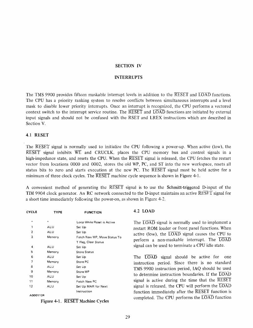
SECTION IV
INTERRUPTS
The TMS 9900 provides fifteen maskable interrupt levels in addition to the RESET and LOAD functions. The CPU has a priority ranking system to resolve conflicts between simultaneous interrupts and a level mask to disable lower priority interrupts. Once an interrupt is recognized, the CPU performs a vectored context switch to the interrupt service routine. The RESET and LOAD functions are initiated by external input signals and should not be confused with the RSET and LREX instructions which are described in Section V.
4.1 RESET
The RESET signal is normally used to initialize the CPU following a power-up. When active (low), the RESET signal inhibits WE and CRUCLK~ places the CPU memory bus and control signals in a high-impedance state, and resets the CPU. When the RESET signal is released, the CPU fetches the restart vector from locations 0000 and 0002, stores the old WP, PC, and ST into the new workspace, resets all status bits to zero and starts execution at the new PC. The RESET signal must be held active for a minimum of three clock cycles. The RESET machine cycle sequence is shown in Figure 4-1.
A convenient method of generating the RESET signal is to use the Schmitt-triggered D-input of the TIM 9904 clock generator. An RC network connected to the D-input maintains an active RESET signal for a short time immediately following the power-on, as shown in Figure 4-2.
CYCLE TYPE
ALU
2 ALU
3 Memory
4 ALU
5 Memory
6 ALU
7 Memory
8 ALU
9 Memory
10 ALU
11 Memory
12 ALU
AOOO1124
Figure 4-1.
FUNCTION
Loop While Reset is Active
Set Up
Set Up
Fetch New WP, Move Status To
T Reg, Clear Status
Set Up
Store Status
Set Up
Store PC
Set Up
Store WP
Set Up
Fetch New PC
Set Up MAR for Next
Instruction
RESET Machine Cycles
29
4.2 LOAD
The LOAD signal is normally used to implement a restart ROM loader or front panel functions. When active (low), the LOAD signal causes the CPU to perform a non-maskable interrupt. The LOAD signal can be used to terminate a CPU idle state.
The LOAD signal should be active for one instruction period. Since there is no standard TMS 9900 instruction period, IAQ should be used to determine instruction boundaries. If the LOAD signal is active during the time that the RESET signal is released, the CPU will perform the LOAD function immediately after the RESET function is completed. The CPU performs the LOAD function

+5
> ~R ">
RESET ~ D
I I
l.----a--TL----I° ) A0001125 C
TIM 9904 (SN74LS362)
CLOCK
GENERATOR
Q
TMS 9900 CPU
--RESET
*R AND C VALUES SHOULD BE CALCULATED AS FUNCTION OF VCC RISE TIME.
Figure 4-2. RESET Generation
by fetching the LOAD vector from addresses FFFC16 and FFFEI 6, storing the old WP, PC, and ST in the new workspace, and starting the LOAD service routine at the new PC, as shown in Figure 4-3.
An example of the use of the LOAD signal is a bootstrap ROM loader. When the LOAD signal is enabled, the CPU enters the service routine, transfers a program from peripheral storage to RAM, and then transfers control to the loaded program.
Figure 4-4 illustrates the generation of the LOAD signal for one instruction period.
4.3 Maskable Interrupts
The TMS 9900 has 16 interrupt levels with the lower 15 priority levels used for maskable interrupts. The maskable interrupts are prioritized and have transfer vectors similar to the RESET and LOAD vectors.
4.3.1 Interrupt Service
CYCLE TYPE FUNCTION
ALU Set Up
2 Memory Read Fetch New WP
3 ALU Set Up
4 Memory Write Store Status
5 ALU Set Up
6 Memory Write Store PC
7 ALU Set Up
8 Memory Write Store WP
9 ALU Set Up
10 Memory Read Fetch New PC
11 ALU Set Up MAR for Next
Instruction AOOOl126
Figure 4-3. LOAD Machine Cycle Sequence
A pending interrupt of unmasked priority level is serviced at the end of the current instruction cycle with two exceptions. The first instruction of a RESET, LOAD, or interrupt service routine is executed before the CPU tests the INTREQ signal. The interrupt is also inhibited for one instruction if the current instruction is a branch and load workspace pointer instruction (BLWP) or an extended operation (XOP). The one instruction delay permits one instruction to be completed before an interrupt context switch can occur. A LIMI instruction can be used as the first instruction in a routine to lock out higher priority maskable interrupts.
The pending interrupt request should remain active until recognized by the CPU during the service routine. The interrupt request should then be cleared under program control. The CRU bit manipulation instructions can be used to recognize and clear the interrupt request.
30

+5 +5 0 0
+5 - 0 0 0 0
%SN74LS74 %SN74LS74 TMS 9900
CPU
-) n-O LOAD -j i I I
CL CL LOADCK
L y +5
lAO
AOOOl127
Figure 4-4. LOAD Generation
The interrupt context switch causes the interrupt vector to be fetched, the old WP, PC, and ST to be saved in the new workspace, and the new WP and PC to be loaded. Bits 12-15 of ST are loaded with a value of one less than the level of the interrupt being serviced. The old \VP, PC, and ST are stored in the new workspace registers 13, 14, and 15. When the return instruction is executed, the old WP, PC, and ST are restored to the CPU. Since the ST contains the interrupt mask, the old interrupt level is also restored. Consequently, all interrupt service routines should terminate with the return instruction in order to restore the CPU to its state before the interrupt.
The linkage between two interrupt service routines is shown in Figure 4-5, and the interrupt machine cycle sequence is shown in Figure 4-6.
4.3.2 Interrupt Signals
The TMS 9900 has five inputs used for maskable interrupts. The INTREQ signal is active (low) when a maskable interrupt is pending. If INTREQ is active at the end of the instruction cycle, the CPU compares the priority code on ICO through IC3 to the interrupt mask (STI2-STI5). If the interrupt code of the pending interrupt is equal to or less than the current interrupt mask, the CPU executes a vectored interrupt; otherwise, the interrupt request is ignored. The interrupt priority codes are shown in Table 4-1. Note that the level-O interrupt code should not be used for external interrupts since level 0 is reserved for RESET.
Figure 4-7 illustrates the use of the TMS 9901 programmable system interface for generation of the interrupt code from individual interrupt input lines. The TMS 9901 provides six dedicated and nine programmable latched, synchronized, and prioritized interrupts, complete with individual enabling/disabling masks. Figure 4-8 illustrates the use of an SN74148 priority encoder and an SN74373 octal latch to provide a TTL eight-input interrupt system. Synchronization prevents transitions of ICO-IC3 while the code is being read. A single-interrupt system with an arbitrarily chosen level-7 code is shown in Figure 4-9. The single-interrupt input does not need to be synchronized since the hardwired interrupt code is always stable.
31

WRO
WRl
PROGRAM A
GENERAL MEMORY
PROGRAM B
GENERAL MEMORY
WORKSPACE 8
WR13 WP (A)
WR14 PC (A)
WR15 ST (A)
GENERAL MEMORY
WRO
WORKSPACE A
WR15
Figure 4-5. Interrupt Linkage
4. 3. 3 Interrupt Masking
TMS 9900
PC (8)
WP (8)
ST (8)
The TMS 9900 uses a four-bit field in the status register, ST12 through ST15, to determine the current interrupt priority level. The interrupt mask is automatically loaded with a value of one less than the level of the maskable interrupt being serviced. The interrupt mask is also affected by the load interrupt mask instruction (LIM!).
Since the interrupt mask is compared to the external interrupt code before an interrupt is recognized, an interrupt service routine will not be halted due to another interrupt of lower or equal priority unless a LIMI instruction is used to alter the interrupt mask. The LIMI instruction can be used to alter the interrupt-mask level in order to disable intervening interrupt levels. At the end of the service routine, a return (RTWP) restores the interrupt mask to its value before the current interrupt occurred.
32

CYCLE
2
3
4
5
6
7
8
9
10
11
AOOO1129
Figure 4-6.
VCC
~ <:> ~
IN
!
A0001130
TYPE FUNCTION
ALU Set Up
Memory Read Fetch New WP
ALU Set Up
Memory Write Store Status
ALU Set Up
Memory Write Store PC
ALU Set Up
Memory Write Store WP
ALU Set Up
Memory Read Fetch New PC
ALU Set Up MAR for Next
Instruction
Interrupt Processing Machine Cycle Sequence
~ .vu· ...... ...,
A 10-A14
TMS 9900 CRUIN
CRUOUT
CRUCLK
~ .. ¢1-¢4
0
RST I -<;>3
TIM 9904 (SN14LS362)
Note that the TMS 9900 actuaHy generates the interrupt vector address using ICO-IC3 five clock cycles after it has sampled INTREQ and four clock cycles after it has compared the interrupt code to the interrupt mask in the status register. Thus, interrupt sources which have individual masking capability can cause erroneous operation if a command to the device to mask the interrupt occurs at a time when the interrupt is active and just after the TMS 9900 has sampled INTREQ but before the vector address has been generated using ICO-IC3.
The individual interrupt masking operation can be easily allowed if the masking instruction is placed in a short subroutine which masks all interrupts
SYSTEM INTERRUPTS
CE--~-C
~ v
TMS 9901
- I ... RST1 -
¢
Figure 4-7. Systern \Vith 15 External Interrupts
33

TABLE 4-1. INTERRUPT PRIORITY CODES
Vector Location Interrupt Level (Memory Address
In Hex)
(Highest priority) 0 00 1 04 2 08 3 DC 4 10 5 14 6 18 7 1C 8 20 9 24
10 28 11 2C 12 30 13 34 14 38
(Lowest priority) 15 3C
* Level 0 can not be disabled.
4>3
-:J V'
INTERRUPT SIGNAL 1 -I I I I
SN74LS373 I OCTAL I LATCH I
I INTERRUPT SIGNAL 8 '-
I
A0001131
Device Assignment
Reset External device
External device
~ :t7 El
SN74148 (TIM 9907)
:: 0
Interrupt Mask Values To Interrupt Enable Respective Interrupts Codes
(ST12 thru ST15) ICO thru IC3
o through F* 1 through F 2 through F 3 through F 4 through F 5 through F 6 through F 7 through F 8 through F 9 through F A through F B through F C through F D through F
E and F F only
GSp
+5
A2 b
Al :::>.
AO 0-
0000 0001 0010 0011 0100 0101 0110 0111 1000 1001 1010 1011 1100 1101 1110 1111
INTREQ
ICO
ICl
TMS 9900 IC2
1C3
* LEVELS 8-15 USED; LEVELS 0-7 CAN BE USED BY GROUNDING ICO
Figure 4-8. Eight-Input Interrupt System With Synchronization
with a LIMI 0 instruction before individually masking the interrupt at the device, as shown in Figure 4-10.
4. 3.4 Interrupt Processing Example
The routine in Figure 4-11 illustrates the use of the LIMI instruction as a privileged or non-interruptable instruction. The level-S routine sets a CRU·bit and then loops until a corresponding CRU bit is true. The
34

first instruction in the routine is completed before a higher priority interrupt can be recognized. The LIMI instruction, however, raises the CPU priority level to level 0 in order to disable all other maskable interrupts. Consequently, the level-5 routine will run to completion unless a RESET signal or a LOAD signal is generated. At the end of the routine, the RTWP instruction restores the CPU to its state before the level-5 interrupt occurred.
INCORRECT
XXX
SBO
YYY
CORRECT
XXX
BLWP
xxx x
SB1 LlMI
MOV
SBO
RTWP
SBW BSS
AOOO1133
INTERRUPT
+5
A0001132
INTREQ
ICO
IC1
IC2
IC3
TMS 9900
Figure 4-9. Single-Interrupt System
0
9
0
@24(13),12
0
32
SET MASK (INTERRUPT CAN OCCUR
DURING SBO CAUSING ERRONEOUS
OPERATION)
(WR9) = ADDRESS OF SBW
(WR10) = ADDRESS OF SB1
CLEAR STATUS MASK TO INHIBIT INTERRUPTS
MOVE CRU BASE ADDRESS TO WR12
SET MASK
RETURN
SUBROUTINE WORKSPACE
Figure 4-10, External Interrupt Clearing Routine
35

Level 5 L1MI 0 Disable Maskable INTREQs
SBO ACK Set CRU Output Bit
Loop TB ROY Test CRU Input Bit
JNE LOOP Loop Until Input True
RTWP Return AOOO1134
Figure 4-11. LIMI Instruction Routine
36

SECTION V
INPUT/OUTPUT
The TMS 9900 has three I/O modes: direct memory access (DMA), memory mapped, and communications register unit (CRU). This multi-mode capability enables the designer to optimize a TMS 9900 I/O system to match a specific application. One or all modes can be used, as shown in Figure 5-1.
5.1 Direct Memory Access
DMA is used for high-speed block data transfer when CPU interaction is undesirable or not required. The DMA control circuitry can be relatively complex and expensive when compared to other I/O methods.
5.2 Memory Mapped I/O
Memory mapped I/O permits I/O data to be addressed as memory with parallel data transfer through the system data bus. Memory mapped I/O requires a memory bus compatible interface; that is, the device is addressed in the same manner as a memory, thus the interface is identical to that of memory. Figure 5-2 shows a memory mapped I/O interface with eight latched outputs and eight buffered inputs. In using memory mapped I/O for output only, care must be taken in developing the output device strobe to ensure it
CRU
AOOOl135
CRUIN
r.RUCLK
j:RUOUT
TMS 9900
ADDRESS BUS
11 SYSTEM MEMORY
MEMORY MAPPED
I/O
~ I~ __ ~ __ ~ MEMORY
-V ~ .......... iIo- ""II.......... CON1ROL
5
D DMA
)~ ______________ D_AT_A_B_U_S __________ ~~L-________ ~( DMA CONTROL --, 16
~--------~I~·~----~~~~~~----------------------------------~
.. COMMUNICA liONS REGISTER UNIT - CRU • MEMORY MAPPED 1/0
• DIRECT MEMORY ACCESS - DMA
Figure 5-1. TMS 9900 I/O Capability
37

FROM TMS9900
WE
DBIN
ADDRESS DEVSEL
DECODE
AOOOl136
SN74 LS347
10-80
DO-D7 E
% SN74LS139
SN74LS241 A 0
B 1Y1-1Y4, 1A1-1A4,
2 2Y1-2Y4 2A 1-2A4
G 3 1G 2G
Figure 5-2. 8-Bit Memory Mapped I/O Interface
8 LATCHED AND BUFFERED OUTPUTS
8 BUFFERED INPUTS
is not enabled during the initial read of the memory address, since the TMS 9900 family of processors first reads, then writes data to a memory location in write operations. This can be effectively accomplished by using the processor write control signal WE in decoding the output address.
5.3 Communication Register Unit (CRU)
CRU I/O uses a dedicated serial interface for I/O. The CRU instructions permit transfer of one to sixteen bits. The CRU interface requires fewer interface signals than the memory interface and can be expanded without affecting the memory system. In the majority of applications, CRU I/O is superior to memory mapped I/O as a result of the powerful bit manipUlation capability, flexible field lengths, and simple bus structure.
The CRU bit manipUlation instructions eliminate the masking instructions required to isolate a bit in memory mapped I/O. The CRU multiple-bit instructions allow the use of I/O fields not identical to the memory word size, thus permitting optimal use of the I/O interface. Therefore, the CRU minimizes the size and complexity of the I/O control programs, while increasing system throughput.
The CRU does not utilize the data bus which is used only for system memory. This can reduce the complexity of printed circuit board layouts for most systems. The standard 16-pin CR U I/O devices are less expensive and easier to insert than larger, specially designed, memory mapped I/O devices. The smaller I/O devices are possible as a result of the serial CRU bus which eliminates the need for several pins dedicated to a parallel-data bus with multiple control lines. System costs are lower because of simplified circuit layouts, increased density, and lower component costs.
38

5.3.1 CR U Interface
The interface between the TMS 9900 and CRU devices consists of AO-A14, CRUIN, CRUOUT, and CRUCLK as shown in Figure 5-1. AO-A2 indicate whether data is to be transferred and A3-A14 contain the address of the selected bit for data transfers; therefore, up to 212 or 4,096 bits of input and output may be individually addressed. CRU operations and memory-data transfers both use AO-A14; however, these operations are performed independently, thus no conflict arises.
5.3.2 CR U Machine Cycles
Each CRU operation consists of one or more CRU output or CRU input machine cycles, each of which is two clock cyles long. As shown in Table 5-1, five instructions (LDCR, STCR, SBO, SBZ, TB) transfer data to or from the TMS 9900 with CRU machine cycles, and five external control instructions (IDLE, RSET, CKOF, CKON, LREX) generate control signals with CRU output machine cycles.
TABLE 5-1. INSTRUCTIONS GENERATING CPU CYCLES
Instruction Number of Type of Data
CRU Cycles CRU Cycles AQ.A2 Transfer
LDCR 1-16 Output 000 Yes
STCR 1-16 Input 000 Yes
SBO 1 Output 000 Yes
SBZ 1 Output 000 Yes
TB 1 Input 000 Yes
IDLE 1 I Output 010 No
RSET 1 Output 011 No
CKOF 1 Output 101 No
CKON 1 Output 110 No
LREX 1 Output 111 No J
5.3.2.1 CRU Output Machine Cycles. Figure 5-3 shows the timing for CRU output machine cycles. Address (AO-A14) and data (CRUOUT) are output on ¢ 2 of clock cycle 1. One clock cycle later, the TMS 9900 outputs a pulse on CRUCLK for Y2 clock cycle. Thus, CR UCLK can be used as a strobe, since address and data are stable during the pulse. Referring again to Table 5-1, it is important to note that output data is transferred only when AO-A2 = 000. Otherwise, no data transfer should occur, and AO-A2 should be decoded to determine which external control instruction is being executed. These external control instructions may be used to perform simple control operations. The generation of control strobes for external
instructions and a data transfer strobe (OUTCLK) is illustrated in Figure 5-4. If none of the external control instructions is used, AO-A2 need not be decoded for data transfer since they will always equal 000.
5.3.2.2 CRU Input Machine Cycles. The timing for CRU input machine cycles is shown in Figure 5-5. The address is output at the beginning of the first clock cycle. The CRUIN data input is sampled on 01 of clock cycle 2. Thus, CRU input is accomplished by simply multiplexing the addressed bit onto the CRUIN input. AO-A2 will always be 000, and may be ignored. CRU input machine cycles cannot be differentiated from ALU cycles by external logic, thus no operations (such as clearing interrupts) other than CRU input should be performed during CRU input machine cycles.
5.3.3 CR U Data Transfer
The CRU base address is defined by bits 3-14 of the current WR12 when a CRU data transfer is performed. Bits 0-2 and bit 15 of WR12 are ignored for CRU address determination.
39

5.3.3.1 Single Bit Instructions. For single-bit CRU instructions (SBO, SBZ, TB), the address of the CRU bit to or from which data is transferred is determined as shown in Figure 5-6. Bits 8-15 of the machine code instruction contain a signed displacement. This signed displacement is added to the CRU base address (bits 3-14 of WR12). The result of this addition is output on A3-A14 during the CRU output or the CRU input machine cycle.
z .... 0 ~t= .... « ~a: o~
I CLOCK I CLOCK I
CYCLE 1 CYCLE 2
~ ~ ~ ~
AO - A14 ::x CRU BIT ADDRESS n x: CRUCLK ~
--------,~ ,-----
o CRUOUT:X CRU DATA OUT n x::
For example, assume the instruction "SBO 9" is executed when WR12 contains a value of 10401 6'
The machine code for "SBO 9" is 1 D09 1 6 and the signed displacement is 000916 , The CRU base address is 082016 (bits 0-2 and bit 15 are ignored). Thus, the effective CRU address is 082016 + 000916 = 0829 16 , and this value is output on AO-AI4 during the CRU output machine cycle.
A0001137
Figure 5-3. CRU Output Machine Cycle Timing
As a second example, assume that the instruction "TB-32" is executed when WR 12 = 10016 , The effective CRU address is 8016 (CRU base) + FFE0 1 6 (signed displacement) = 6016 , Thus, the "TB-32" instruction in this example causes the value of the CRU input bit at address 6016 to be transferred to bit 2 of the status register. This value is operated on by the JEQ or JNE instructions, which cause the PC to be changed depending on the value of ST2.
5.3.3.2 LDCR Instruction. The LDCR may transfer from 1 to 16 bits of output data with each instruction . ... The output of each bit is performed by a CRU output machine cycle; thus, the number of CRU output
machine cycles performed by a LDCR instruction is equal to the number of bits to be transferred.
TO MEMORY AND CRU
15
5 A r-~-----------'-------~~~~B
AO-A14 C
SN74LS138 TMS 9900
~ __ CR_U_C_L_K _____________ ~~Gl
GZA G2B
A0001138
Figure 5-4. CRU Control Strobe Generation
40
LREX
CKOF
CKON
RSET
fO""IT"
OUTCLK (TO CRU)

z
<1>1
<1>2
<1>3
AO· A14
o ... j: ::J <3: CRUIN ~ a:
w Q. o
AOOOl139
I CLOCK I CLOCK i I CYCLE 1 I CYCLE 2 I
l n n"",--_
__ n,--_~n,--_ ..... n
::x: CRU ADDRESS m x:=::: mO:q~'tf~~¥~
INPUT VALID INPUT BIT m
As an example, assume that the instruction "LDCR @ 600,10" is executed, and that WR12 = 800 16
and the memory word at address 600 contains the bit pattern shown in Figure 5-7. In the first CRU output machine successive machine cycle the address is incremented by one and the next least-significant bit of the operand is output on r'DTT{)TTT 1l .... t,1 1 n hac 1-,.:"ro hoo .... r\llt .... llt Tt lc '--'~'-V'-...l'U.l.., \.A...1il.~~ ..1 V V.1L-J 11.U'Yv 1.,..1,-"\,,.1.11 VULP"","l.. LL ~J
important to note that the CRU base address is unaltered by the LDCR instruction, even though the address is incremented as each successive bit is output.
Figure 5-5. CRU Input Machine Cycle Timing
5.3.3.3 STCR Instruction. The STCR instruction causes from 1 to 16 bits of CRU data to be transferred into memory. Each bit is input by a CRU input machine cycle.
Consider the circuit shown in Figure 5-8. The CRU interface logic multiplexes input signals m-t onto the CRUIN line for addresses 200 16 -207 1 6 . If WR 12 @
400 16 when the instruction "STCR @ 602,6" is executed, the operation is performed as shown in Figure 5-9. At the end of the instruction, the six LSBs of memory byte 602 are loaded with m-r. The upper bits of the operand are forced to zero. The generation of SEL200 may be simplified if the total CRU address space
is not used.
o 1 2 3
DON'T CARE
4 5 6
"" BIT 8 SIGN
EXTENDED
7 8 9 10 11 12 13 14 15
I I
+ 8 9 10 11 12 13 14 15
I I I I ?
I I I I
o 1 2 3 4 5 6 7 8 9 10 11 12 13 1<1
I I I I I I I I I ~~----------------vr------------~/ SET TO ZERO EFFECTiVE CRU BIT ADDRESS FOR ALL CRU
OPERATIONS
A0001140
W12 BASE
ADDRESS
SIGNED DISPLACEMENT
ADDRESS BUS
Figure 5-6. TMS 9900 Single-Bit CRU Address Development
41

Memory Address 600 I p 0 n m I k j I h 9 fed c b a I 0~------------~7~8~------------~1'5
AO-A14 =x CRUOUT ==x CRUCLK
AOOOl141
WR12 10 0 0 0
o
400 X 401 X a X b X
n .n
1 0 0 0 10 0 0 0 0 0 0 0 I 7 8 i5
4 o o
CRU Base Address = 40016
402 X 403 X 404 X 405 X 406
c X d X e X X 9
n n n n n Figure 5-7. Multiple-Bit CRU Output
X 407 X 408 X 409 x= X h X X C
n n n
5.3.4 CR U Interface Logic
CR U based I/O interfaces are easily implemented using either TMS CRU peripheral devices such as the TMS 9901 or the TMS 9902, or TTL multiplexers and addressable latches, such as the TIM 9905 (SN74LS25l) and the TIM 9906 (SN74LS259). These I/O circuits can be easily cascaded with the addition of simple address decoding logic.
A3
Ali - SN74LS251 A5
AS (TIM 9905)
-'\. SEL200 A7 ... J DO
As 01 -A9 A14
A 02
A10 A13 B 03
All A12 C 04
AOOOl142
Figure 5-8. Example CRU Input Circuit
m
n
o
p
q
42
5.3.4.1 TTL Outputs. The TIM 9906 (SN74LS259) octal-addressable latch can be used for CRU outputs. The latch outputs are stable and are altered only when the CR UCLK is pulsed during a CRU output transfer. Each addressable latch is ena bled only when addressed as determined by the upper address bits. The least-significant address bits (A12-A14) determine which of the eight outputs of the selected latch is to be set equai to CRUOUT during CR UCLK, as shown in Figure 5-10.
5.3.4.2 TTL Inputs. The SN74LS151 and TIM 9905 (SN74LS25l) octal multiplexers are used for CR U inputs, as shown in Figure 5-11. The

MEMORY
AOOOl144
WR12 I 0 0 0 0 0 1 0 0 I 0 0 0 0 0 0 0 0 I 0~-----------------7~8~------------~~15
2 o o
,~------------v------------~/
CRU BASE ADDRESS = 20016
AO - A14 ==x 200 X 201 X 202 X 203 X 204 X 205 x:= CRUIN m n o p q
MEMORY I 0 0 r q p 0 n m I AOOOl143
ADDRESS 602 0 7
Figure 5-9. Multiple-Bit CRU Input
} OTHER CRU
OUTPUT CIRCUITS
CRUCLKr-----------~~ Gl
TMS 9900 G2A G8B
-:'
CRUOUTr-----__ ----------------------------~
RESET~~--_+-----------------------__ --~~
RESET
Figure 5-10. Latched CRU Interface
ABC
S-
SN74LS259 (TIM 9906)
D
CLEAR
00
al
02
Q3
04
05
06
07
I CJ)
I
I-;:) a. I-;:)
r ~ I )
multiplexers are continuously enabled with eRVIN equal to the addressed input. The TIM 9905 should be used for larger systems since its three-state outputs permit simple "wire-ORing" of parallel-input multiplexers.
43

MEMORY
TMS 9900
OTHER ABC } CRU
INPUT CIRCUITS 0
+5 S G1 7
G2A G2B SN74lS151 2 OR
3 en
SN74lS251 ~ co:::>
(TIM 9905) 4 ~
-:: ~ CRUIN~--------------------------------~ Y 5
6
7
AOOOl145
Figure 5-11. Multiplexer CRU Interface
5.3.4.3 Expanding CRU I/O. A CRU interface with eight inputs and eight outputs is shown in Figure 5-12, using the TMS 9901. An expanded interface with 16 inputs and 16 outputs is shown in Figure 5-13, using TTL devices. The CRU inputs and outputs can be expanded up to 4096 inputs and 4096 outputs by decoding the complete CRU address. Larger I/O requirements can be satisfied by using memory mapped I/O or by using a CRU bank switch, which is set and reset under program control. When reset, the lower CRU I/O bank is selected, and when set, the upper CRU I/O bank is selected. In actual system applications, however, only the exact number of interface bits required need to be implemented. It is not necessary to have a 16-bit CRU output register to interface a 10-bit device.
5.4 CRU Paper Tape Reader Interface
CRU interface circuits are used to interface data and control lines from external devices to the TMS 9900. This section describes an example interface for a paper tape reader.
The paper tape reader is assumed to have the following characteristics:
1. It generates a TTL-level active-high signal (SPROCKET HOLE) on detection of a sprocket hole on the paper tape.
2. It generates an 8-bit TTL active-low data which stays valid during SPROCKET HOLE = 1.
3. It responds to a TTL-level active-high command (Paper Tape RUN) signal by turning on when PTRUN = 1 and turning off when PTRUN = O.
44

~I NTERRUPTS (Sly
AOOO1146
I I I
I I
I I
~ « N .... «
y
SN74LS251 (TIM 9905)
0 7 . . . . . . \: )
INPUTS 8-15
AOOO1147
CRUClK
I CRUOUT
I CRUIN
I !
I I A10-A14
CE I I INTERRUPT IIF
r ,~ ~ V f -...-
TMS 9901
0 7 0 7
t •••••• t ~ ...... ~ ~ ----/--
8 INPUTS 8 OUTPUTS
Figure 5-12. 8-Bit CRU Interface
I I I I I I I
All
o:t
~ ~ All «
y G D
SN74LS251 SN74LS259 (TIM 9905) (TIM 9906)
-TMS 9900 I
~ -/
- -1
I RESET
I I
~------------------~I ~~ I ""
ADDRESS
1--------------4 CRUI N
1------+------4 CRUOUT
1---....... ---1------4 CRUCl K
G
SN74LS259 (TIM 9906)
D
TMS 9900 CPU
0 7 00 07 00 07 . . . . . . . . . . . . . . . . :; \. -l \ -l
INPUTS OUTPUTS OUTPUTS 0-7 0-7 8-15
Figure 5-13. 16-Bit CRU Interface
45

5.4.1 Operation
Figure 5-14 illustrates the circuitry to interface the reader to the CRU. The interface is selected when PTRSEL = 0; PTRSEL is decoded from the AO-All address outputs from the TMS 9900. Thus, the output of the SN74LS251 is active only when PTRSEL = 0; otherwise, the output is in high impedance and other devices may drive CRUIN. The data inputs are selected by A12-A14 and inverted, resulting in active high data input on CRUIN. The positive transition of SPROCKET HOLE causes PTRINT to go low. PTRINT is the active low interrupt from the interface. PTRINT is set high, clearing the interrupt, whenever a CRU output machine cycle is executed and the address causes PTRSEL to be active. \Vhen a one is output, PTRUN is set, enabling the reader, and the reader is disabled when a zero is output to the device. Thus, any time PTRUN is set or reset, the interrupt is automatically cleared.
DATAO
DATA1
DATA2
DATA INPUTS DATA3 FROM PAPER TAPE READER DATA4
DATA5
DATA6
DATA7
SPROCKET HOLE
A0001148
~
..
..
....
..
~
-
+5
1 PTRUN
PR CRUOUT a 0
% SN74LS74 PTRCLK
CRUCLK Q I -.J
CLR
T +5 PTRSEL
DO
01
02 w~ CRUIN
SN74LS251
~PTRSEL 03 D4 TIM 9905)
05 S
D6
07 C B A
A14
A13
A12
+5
A PR
'---- 0 Q
Y, SN74LS74
Q--~ PTRINT
----
CLR
r PTRCLK
Figure 5-14. Paper Tape Reader Interface
46
CRU IIF
}
DECODED PAPER TAPE READER ADDRESS (DECODED FROM AO· All)
) ADDRESS BUS
~ PAPER TAPE READER INTERRUPT
J ~~~~~~~=~PT

5.4.2 Software Control
The software routine in Figure 5-15 controls the paper-tape reader interface described above. It is a re-entrant procedure that can be shared by several readers. The assumptions are that:
1. Each reader has its own workspace which is set up on the trap location for that reader's interrupt.
2. The workspace registers are allocated as shown in Figure 5-15.
3. The CRU input bits 0-7 (relative to CRU base) are reader data. CRU output bit 0 con troIs PTR UN and clears the interrupt.
The procedure has two entry points. It is entered by a calling routine at PTRBEG to start the reader and it returns control to that routine. It is entered at PTRINT via interrupt to read a character. The return in this case is to the interrupted program.
PTRINT STCR *R11,8
CB *R11+, R9
JEQ PTREND
DEC R10
JEQ PTREND
PTRBEG SBO PTRUN
RTWP
PTREND SBZ PTRUN
CLR R8
A0001149 RTWP
Figure 5-15. Paper Tape Reader Control Program
The control program may be used by any number of paper-tape reader interfaces, as long as each interface has a separate interrupt level and workspace. As each reader issues an interrupt, the TMS 9900 will process the interrupt beginning at location PTRINT. However, the workspace unique to the interrupting device is used. The organization of memory to control two paper tape readers is shown in Figure 5-16. The interrupt-transfer vector causes the appropriate WP value to be loaded. In both cases PTRINT, the entry point for the control program, is loaded into the PC.
5.5 TMS 9902 Interface
This section describes an example CRU interface using the TMS 9902 asynchronous communications controller. The TMS 9902 transmits and receives data over a serial communications link. It performs its own baud rate generation, parity and format generation, and error checking, and additionally provides an internal interval timer with interrupt capability. The TMS 9902 interfaces directly with the TMS 9900 family CRU with a minimum of additional logic required only for chip-select decode.
5. 5.1 Operation
Figure 5-1 7 illustrates the circuit for the TMS 9902 interface. The CPU uses LDCR and STCR instructions to transfer character data, and TB, SBO, and SB2 instructions to test and to alter the status and control bits.
The TMS 9902 sets RBRL to a logic one and generates an interrupt request via the TMS 9901 programmable systems interface whenever a received character is ready to be read. It correspondingly sets
47
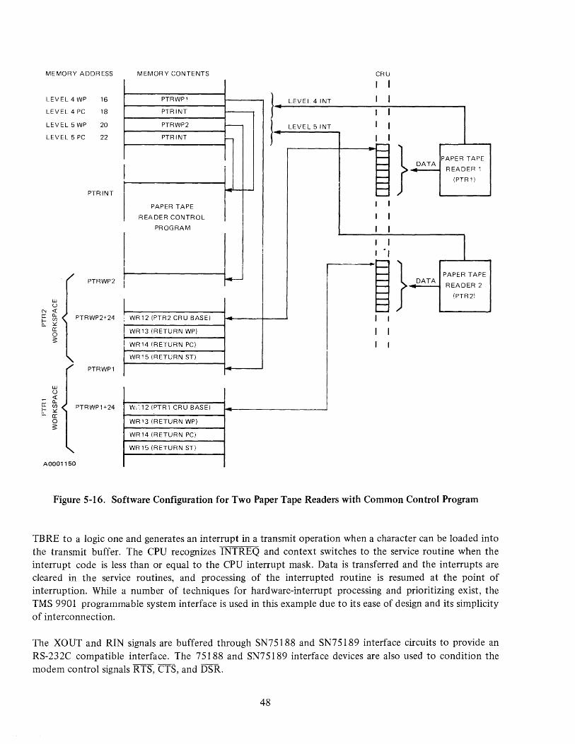
MEMORY ADDRESS
LEVEL4WP 16
LEVEL 4 PC 18
LEVEL 5 WP 20
LEVEL 5 PC 22
PTRINT
PTRWP2
UJ U
N <i a: a.. PTRWP2+24 f-- Ul a.. ~
a: 0 s:
PTRWP1
UJ u <i
0:: a.. Ul PTRWP1+24 t ~ a: 0 s:
AOOO1150
MEMORY CONTENTS
PTRWp1
PTRINT
PTRWP2
PTRINT
I PAPER TAPE
READER CONTROL
PROGRAM
I
: WR12(PTR2CRUBASEI
WR13 (RETURN WP)
WR 14 (RETURN PC)
WR ~ 5 (RETURN ST)
W;~12 (PTRl CRU BASE)
WR 1 3 (RETURN WP)
WR 14 (RETURN PCi
WR 15 (RETURN ST)
--
!
~
CRU
I
1~_L_E_V_E_L_4_'_N_T __________ ~ ____________ -,
I LEVEL 5 INT .....----
}
PAPER TAPE
DATA~ READER i
(PTR1)
DATA PAPER TAPE
READER 2
(PTR2)
Figure 5-16. Software Configuration for Two Paper Tape Readers with Common Control Program
TBRE to a logic one and generates an interrupt in a transmit operation when a character can be loaded into the transmit buffer. The CPU recognizes INTREQ and context switches to the service routine when the interrupt code is less than or equal to the CPU interrupt mask. Data is transferred and the interrupts are cleared in the service routines, and processing of the interrupted routine is resumed at the point of interruption. While a number of techniques for hardware-interrupt processing and prioritizing exist, the TMS 9901 programmable system interface is used in this example due to its ease of design and its simplicity of interconnection.
The XOUT and RIN signals are buffered through SN75188 and SN75189 interface circuits to provide an RS-232C compatible interface. The 75188 and SN75189 interface devices are also used to condition the modem control signals RTS, CTS, and DSR.
48

DSR
'---..JV"\Ar-e--,+5 V
+5 V
SERIAL TRANSMI T-----.----< DATA 330r SERIAL pF _
~~~~~---~XOUT
RECEIVE DATA
A0001151
5.5.2 Software Routines
L}------!RIN Q ~---~
..-v'"fVo- +5 V
13 Kn
TMS 9902 iNf
SO-54
.--------+----ICRUOUT ~~------~--~CRUCLK
A 11-A14 TMS 9900
.-r--t------+---.-4CR UIN
SO-54 ¢~------e
iNT6
TMS 9901 ICO-IC4
CE
¢ ¢1 ¢2 ¢3 ¢4
3 TiM 9904 D
Figure 5-17. TMS 9902 Interface
The software routines in Figure 5-18 control the TMS 9902. The initialization routine can be a part of the normal system power-up reset. Upon being reset the device is cleared and all load flags are set. Loading the control register with A21 6 sets the device for seven bits per character, even parity, one stop bit, and sets the internal clock rate at one-third the system clock rate. Loading the control register also resets the load control register flag, setting up the next register, the timer interval register, to be loaded. In this example,
49

DEVICE INITIALIZATION
LI R12, >40
SBO 31
LDCR @CTL,8
SBZ 13
LDCR @ RDR, 12
CTL BYTE >A2
RXDR BYTE <4DO
TRANSMIT OPERATION INITIALIZATION
XMTOP LI RO, DATAD
LI R1, DATCNT
LI R12,CRUBAS
SBO 16
SBO 19
B *R11
RECEIVE OPERATION INITIALIZATION
RCVOP LI R1, RCVBUF
LI R2,BLVCNT
LI R3, EOB
SBO 18
B *R11 EOB BYTE >OD
INTERRUPT SERVICE ROUTINE
INT6 TB 21
JEQ RCV
TB 22
JEQ XMT
RTWP
XMT LDCR *ROt,8
DEC R1
JEQ XMTEND
RTWP
XMTEND SBZ 19
RTWP
RCV TB 9
JEQ RCVERR
STCR *R1,8
SBZ 18
DEC R2
JEQ RCVEND
CB *R1+, R3
JEQ RCVEND
RTWP
RCVEND SBZ 18
RTWP
AOOO1152
INITIALIZE CRU BASE
RESET DEVICE AND SET LOAD FLAGS
LOAD CONTROL REGISTER AND RESET CTL LOAD FLAG
RESET INTERVAL LOAD FLAG
LOAD READ DATA RATE REG.,
LOAD XMT DATA RATE REG. & RESET LRDR, LXDR
7 BITS/CHAR, EVEN PARITY, 1 STOP BIT, 0 DIVIDE BY 3
300 BAUD OPERATION
INITIALIZE DATA ADDRESS
INITIALIZE DATA COUNT
INITIALIZE CRU BASE
TURN TRANSMITTER ON
ENABLE TRANSMIT INTERRUPTS
RETURN
INITIALIZE BUFFER ADDRESS
INITIALIZE RCV ~OUNT
INITIALIZE EOB CHARACTER
ENABLE RCV INTERRUPTS
RETURN
END OF BLOCK CHARACTER
RCVR INTERRUPT?
YES
XMTR INTERRUPT?
YES
NOT EITHER, GO HOME
TRANSMIT CHARACTER
DECREMENT COUNTES
END IT IF FINISHED
RETURN
MASK XBRE INTERRUPT
RETURN
RECEIVE ERROR?
YES, GO PROCESS IT
STORE CHARACTER
RESET RBRL
BLOCK FULL
YES, EXIT
NO; EOBCHARACTER?
YES; EXIT
GO HOME
INHIBIT RCV INTERRUPTS
Figure 5-18. TMS 9902 Control Programs
50

the timer is not used so the load timer register flag is reset, enabling the loading of the receive data rate register and the transmit data rate register. Here both transmit and receive data rates are set for 300-baud operation.
To initiate an input or output operation the receive or transmit initialization routines are executed to set up the desired operation. From that point the operation is interrupt driven by the INT signal from the TMS 9902.
5.6 Software - UART
Some systems may not require the full capabilities offered by an external UART. For example, a small system can be interfaced to a 733 ASR for initial program loading only. The transmission is used in half-duplex and the program has no significant tasks to perform between input characters. A software-UART function can be used in which the program serially inputs and outputs bits with software format conversion. The system in Figure 5-19 uses a software-UART program to minimize the system component count at the expense of added software.
The software-UART consists of a receive routine and a transmit routine which are called by XOP or BLWP instructions. The routines share a common workspace and a common delay subroutine. The seven-bit plus parity transmit and receive characters are passed through register 0 of the calling program. Since the software-UART routines must run to completion, the interrupt mask is cleared to disable all maskable interrupts. Registers 4, 5, 8, and 10 are used for temporary results. Registers 6,7,9, and 12 are initialized by the system restart routine. The delay routines introduce software determined delays equal to half-bit and full-bit times for a 300 bps data terminal. The receive routine rejects input characters with bad parity, false start bits, or missing stop bits. The software-UART routines are shown in Figure 5-20.
MEMORY A12-A 14
AO-A14 CRUCLK r------t
CRUOUT r-------------
CRUI N r------------.
Y S ABC D ABC
SN74LS151 SN74LS259 (TIM 99061
0 1·7 00 01--07 TMS 9900
7 7
OTHER SYSTEM OTHER SYSTEM
INPUTS OUTPUTS
SERIAL TRANSMIT
~----------------SERIAL RECEIVE AOOOl153
Figure 5-19. Software UART CRU Interface
51

A0001154
001 002 00::: 004 005 006 OO? 00::: 009 010 011 012 01 ": 014 015 016 01;" 01:3 01 ':j 020 021
IDT "S:lt,IUART'
• PEGI:TEP EQUATES
04 ",:4 05 F.~'5
06 P.6 07 f=:'(
08 P8 09 P'''1 01'1 1"10 OB Pll oe P12 OD P13 ·
EGiU 4 EGIU 5 EGIU 6 EGIU ;' EGIU ::: EGIU 9 EQU 10 EGiU 11 EI)U 12 EGIU 13
• CPU EGIUATES · 0000 CPUBAS E9U 0000 INBIT EQU 0000 OUTBIT EQU
PAGE 0001
::OFTWARE UAFH CONT~Ol PROGR~
LOOP COUNTE~ BIT COUNT HALF-BIT DELAY LINi(A6E FULL-BIT DELAY LINKAGE CHARACTER ACCUMULATOR BIT MAS~ .8(00) :;.CRATCH LI N~:AGE CRU BASE ",'ETURI"l I,jP
CPU BASE ADDRESS PECE I 'y'E r NPUT TPANSMIT OUTPUT
022 023
• HALF-SIT AND FULL-BIT TIME DELAY SUBROUTINES
024 025 026 027
• nnRY: BL BL
.P6 FOR HALF-BIT DELAY
.p;" FOP FULL-BIT DELAY
• P6 = HBIT, P;" = FBIT 02':: 02'''1 OOF:3 HBDL""! 03u 0000 FBIT 031 000 C2:3B 0";:2 00;:: 06'~6
O?"3 004 C2CA 034 0006 HBIT 035 000'::=. 0204
000:::: nOF:3
EI;lU 24:3 EQU S MO'y' P 11 , RIO BL .P6 MO'.,.' ~'1 O. ",'11 EOU S LI R4, HBDL Y
0001'1 0604 DLOOP DEC R4 000': 16FE -,r'iE DLOOP OOOE 04'5B ",'T
• RECEIVER CONTROL PROGRAM
HALF-BIT DELAY COUNT FULL-BIT DELAY ENTRY :WiE L I N~: AI~E CALL HALF-BIT DELAY ~'E : TD",'E L I N~ AGE ~ALF-BIT DELAY ENTRY INITIALIZE LOOP COUNTER
DECREMEI"lT cou~n
LOOP U~TIL END OF DELAY RETURN
0036 00:37 00::::: ')040 0041 0042 0043 0044 0045 004";, 0047 004:? OU4'?
• UPON PETUPN TO CALLING PROGRAM. THE LEFT BYTE OF • I,IF'O OF THE ::ALLING PPOI::;PAM cmnAIN: THE RECEI'y'ED • CHARACTER. CHARACTERS WITH PARITY OP FRAMING • EPRORS ARE IGNORED.
0050 0010 FC~
0051 OU1 0 :)~:OO
00l~' 0000 0052 0014 0205
Ej~U oj.
L IMI 0
:....1 P5. :::
0053 0018 IFno PLOOPI TB INBIT (1054 0('11'1 1 ":FE -,Ee' ~'LOOPI
0055 OOlC 1)-:,36 BL .F;'6 ,)(t",~ O':rtE l~rlO TB PiPIT 005- 0020 13FB -'EQ PLOOPI 0053 0022 06~~ ~LDDP2 BL .P7 I-I(I~';'~ !)024 1-I':'1'~ =,F'L J;"::~ 1
~060 0026 IFOO TB INBIT i:1 0,:, 1 (102':: le,-- JiiE r:;'=~ IF (1(1,=·2 OO,::H Ec.'O'~ :01: ~,,?, ~':3
I)I.I,,:.~: OO~'I= 0-:.05 ~"~!<. IP DEC ~'5
002'::··1601 !:I::t':.4 (l1:12E 16F'? (IOt::.:, 0 I)':: (I 0,:.'3 (' OOt::.~, OO~:2 IFOO
-'tiE PLOOP2 ~L. .P7 TB HiBIT
l:il:I':.;-" Or:I:'::~ l~,ED J:"it:: PI:'",' 0068 0036 D748 MOVB P8,.RI3 (":r.:,'~ 0'-',:':: 1(-- JOF' ",'E>':IT 1:11.1 ," 0 (, (I ,:8 10EA JMP P( ',I ,HI71 1-"-":'- 474'~ ~'E'-:IT ::::C R9 .• ';'13
;::: •• 1': 01 (1(1;-':: I)O:'::E r14-:,B ~'TIIIF'
MA:~ ALL INTERRUPTS
Iril T I ALI ZE BIT:: OUNT
TE:T FOP :TAPT BIT NO.(ONTI~-'E TESTING DELAY ~ALF-BIT TIME
IF FAL:E :TART BIT. :TAPT C"/ER DELA',' FULL-BI T TIME :HIFT FOP NEXT BIT PEAD INF'UT IF HWUT IS 0, :t.IP EL:E:ET M::B LA:T DATA BIT'
no. LOOP YE:. DELAY FULL-BIT TIME TE:T FOR STOP BIT IF EPROF', I GNOPE C HARRe TEl" I F NO EPROP. : TOPE C HAFO'A( TE~ IF F'AP IT\, EPROFO', IGNORE CHAPACTE~ MA:~' PARITY BIT
F'ETUPN
Figure 5-20. Softwaie DART Control Program (Page 1 of 2)
52

A0001154
0074 007-S 0076 0077 0078 007'~ 0080 00:31 00:32 00:3"3 00::::4
00:35 00:36
00::::7 00::::8 008'01 0090
00'011 0(1':;'2
00':;'3 00'0'4 00':;'5 o (I ':;a 6 OO'~7
oo·~:::
oo·~'3
0100 0101 0103 0104 010'S 0106 0107 0108 010'0' 0110 0111
(1112
0113
0114
011'5 0116 0117 0118 0119 0120 0121 0122 0123
0124
0125
0126
0040 0300 0042 0000 0044 04C:::: 0046 020'5 0048 0001'1 004A D21D 004C le--004E 2Ft 0'" 0050 O'O'lB 004( •• 1(01 (1052 E20':;' 0054 0'36:3 00'56 O'?lS 005:3 1:3--00'51'1 lEOO I)O~C 1 0--(lOSE 1DOO (i 1)5.~3 •• 1 :3 02 0000,0 06';'7 (I (l5e •• 1 001 00':.2 0605 0064 1t,FB 0066 0::;::(1
0068 006:3 0206 006A 0006 006C 0207 006E 0000 0070 020':;' 007'2.' :::000 0074 020(: 0076 0000 007:? 04'5B
(l07A
009A 007A' 009C 0068' OO':;'E 007A' OORO 001 (I' 001'12 007A' OOA4 0040"
F'A':;E 0002
• • TRANSMITTER CONTROL P~OG~AM
• ENTRY: BL~P ~XMTYCT
• THE LEFT BYTE OF W~O OF THE CALLING PROGRAM • IS iERIALLY TRANSMITTED. PRECEDED BY A START • BIT, CORRECTED FOR PARITY, AND FOLLOWED • B..,.' A 'STOP BIT.
:'<MT LIM!
CLR P.8 LI PC:I, 1 0
MO',/B .R13, R:3 JOP '<S~ It:' '<DR PSI. P~3
>,:'SKIP SRL RB. 1
SOC P9.R8 :F'L ~':3!16
:<LOOP :I<'L P.8, 1 JOC :-:miE SB': OUTBIT JMF' :qiE:'<T
:<ONE :BO OUTBIT
:'<NE:':T BL .R7
DEC PI)
Jr'iE :':LDOP F'TIJP
· HHTIALIZATION PROI:;RAM
• ENTRY: BLWP iENTVCT
• REGISTERS ARE INITIALIZED
alTER EQIJ i LI t" HBIT
LI 7, FBIT
LI
LI 12,CRUBA:
F'TI,lP
• PROGRAM WORKSPACE
· ENTP"'" TRANSFER '.'ECTOFIS • HITVCT DATA UAFlTWP, ENTER
RC'y'VCT DATA UARTI,oIP. RCV
:,:r'ITVCT DATA UARTI"IP. :.;r"IT
END
MAS~ ALL INTERRUPTS
~LEAR CHARACTER ACCUMULATOR LOAD BIT cou~n
FETCH CHARACTER ': OF'REC T PAR I TY
APPE~m : TOF' BIT RIGHT JU:TIFY CHARACTER :I1IFT OUT UB IF ONE, :ET OUTBIT TO ONE EL:E, SET TO ':EF'O
DELAY FULL-BIT TIME
LA:T BIT7 ~iD. ':ONT HiUE 'i'E:, t=::ETUF'N
anp..,.' POINT HALF-BIT :UBPOUTINE
FULL-BIT :UBPOUTINE
BIT MAS"
CRU BASE ADDRES:
PETURN
INITIALIZATION ENTRY VECTOR
RECEIYER ENTRY VECTOR
TRANSMIT ENTRY VECTOR
END OF PROGRAM
Figure 5-20. Software UART Control Program (Page 2 of 2)
53

5.7 Burroughs SELF-SCAN Display Interface
This section describes a TMS 9900 CRU interface to a Burrough's SELF-SCAN® panel display model SS30132-0070. The display panel has a 32-position, single-row character array with a repertoire of 128 characters.
The panel display operates in a serial-shift mode in which characters are shifted into the panel one at a time. Characters are shifted in right-to-left and can be shifted or backspaced left-to-right. A clear pulse erases the display.
The CRU display interface is shown in Figure 5-21 and a display control subroutine is shown in Figure 5-22. The subroutine is called by one of two XOP instructions, XOPO and XOPI. The calling routine passes
MEMORY
AO-A14
....... --+ ........ --------------1 CRUCLK
111 t----+-+--.----------I CRUOUT
TMS 9900
; CPU
ABC D
SN74LS259 (TtM 99061
OTHER
CRU
OUTPUTS
+5V -12 V
-120V
6
07 01 00
BLANK DATA
PRESENT
<t
ABC
SN74LS259 (T1M 9906)
D
07 Q6 05 04 03 02 01 00
I I CLEAR B 8 8 8 8 8 8 DATA
TAKEN 64 32 16 8 4 2 1
DISPLAY MODEL SS30132-0070
A0001155 Figure 5-21. Display Control Interface
54
CRUIN

the address and length of the output string in registers 8 and 9 of its workspace. The two XOP subroutines share the same workspace and perform the same function except that XOP 1 clears the panel display first. The backspace feature is not used. The panel display is blanked during character entry.
5.8 Matrix Keyboard Interface
EIGHT
NINE
RXOP1
LOOP1
RXOP2
LOOP2
WAIT
A0001156
EOU
EOU
SBZ
LI
DEC
JNE
SBO
SBO
MOV
MOV
LDCR
SBO
TB
JEO
SBZ
DEC
JNE
SBZ
RTWP
8
9
7 Clear Panel
R1,11
R1 Delay>67,usec
LOOP1
7
9 Blank Panel
@EIGHT (13),1 Load Address
@NINE (13),2 Load Length
*1+,7 Output Char
8 Data Present
0 Wait for Data Taken
Wait
8
2 Decrement Count
LOOP2 Loop Until Through
9 Unblank Panel
Return
Figure 5-23 shows how two l6-pin devices and eight resistors can be used to interface a 64-key keyboard connected as a row-column matrix. This circuit requires a 64-bit CRU input-address space. Columns are selected by A9-All, and specific keys in each column are addressed by A12-A14. Therefore, individual keys may be read by the TB (test bit) instruction, or the entire array may be read by four l6-bit STCR instructions, incrementing the CRU base address by 16 between each STCR instruction. Functions such as switch debounce and key rollover may be performed in software. Figure 5-22. Burrough's SELF-SCAN Display
Control Program
AO-A15
3 3 TO
(A9-All) 8
74LS156
3
(A12-A14)
CRUIN~-----4
TMS 9900 74LS251
(TIM 9905)
AOOOl157
8
l Figure 5-23. 64-Key Scanning Circuit
55/56
+5 V


SECTION VI
AUXILIARY SYSTEM FUNCTIONS
This section describes the circuitry and application of several functions which may be useful in a TMS 9900 system.
6.1 Unused Op Codes
The unused op codes for the TMS 9900 are shown in Table 6-1. An instruction which consists of any of these codes will cause the TMS 9900 to perform no operation other than the updating of the PC to point to the next sequential even word address and the processing of RESET, LOAD, and interrupts in the normal way. It is not recommended that any of these codes be used to perform the function of a no-op, however, since future upward-compatible members of the TMS 9900 microprocessor family will use these codes for presently unimplemented instructions. The TMS 9900 assembler has defined the pseudo-instruction "NOP" to generate a code of 1 00016 , which is equivalent to the "JMP $+2" instruction.
6.1.1 Unused Op Code Detection
The occurrence of unused op codes may be detected by the circuitry shown in Figure 6-1. The signal ILOPCD is set high at the end of memory cycle which fetches the unused op code. On the first clock cycle of each instruction fetch, the IAQTl signal is set high. Then, when memory data is read (on the next clock cycle in which the processor is not in a WAIT state) the IAQTl signal is reset and, if ILODEC = 0, the illegal op code flag ILOPCD is set. It may be convenient to use ROM, a PLA, or random logic to generate the signal ILODEC, which is low when any of the unused codes is decoded. If WAIT states do not occur, one SN74LS32 gate may be deleted.
6.1.2 Unused Op Code Processing
The occurrence of an unused op code is an error condition which may be caused by device failure, signal noise, or errors in software. Therefore, the error flag generated should be a high-priority (low-level) interrupt which causes the processor to suspend operation before any further instructions are executed. The flag should be cleared by the CLILOP signal only after the cause of the error is determined.
6.2 Software Front Panel
A useful feature during hardware and software development is a means for controlling the operation of the processor at a more basic level than is required during normal system operation. For instance, it is desirable to start and stop execution of a program segment, to execute single instructions, to inspect and to modify memory and internal registers, and to load programs into RAM. These features are assocIated with the front
57

TABLE 6-1. UNUSED OP CODES
BINARY HEXADECIMAL
0 1 2 3 4 5 6 7 8 9 10 11
0 0 0 0 - 0 1 F F 0 0 0 0 0 0 0 x x x x x
0 3 2 0 - Q 3 3 F 0 0 0 0 0 0 1 1 0 0 1 x
0 7 8 C - 0 7 F F 0 0 0 0 0 1 1 1 1 x x x I I 0 C 0 o
ROM, PLA OR
RANDOM LOGIC
DO D10 UNUSED OPCODE ILODEC DECODE
FROM WAiT
TMS 9900
VCC
A l lAO PR IAOT1
Ul
K 0 IAQT1
CLR
VCC
FROMSYSTEM{ ___ P~l~T~T~L~l~_I ______________________________________ ~ CLOCK
Ul - SN74L S109 U2 - y.. SN74LS32 U3 -- y.. SN74LS02
12 13 14 15
x x x x
x x x x
x x x x
x x i
VCC
6 PR
Ul
II K
CLR
CLEAR ILLEGAL { CLILOP OPCODEFLAG ~.~------------------------------
AOOOl158
Figure 6-1. Illegal Op Code Detection Circuitry
0 ILOPCD
0 !LOPCD
panel of a conventional minicomputer and are normally implemented in hardware. Similar capabilities may be provided for any TMS 9900 system very economically using a combination of hardware and software.
6.2.1 System Configuration for Software Front Panel
Figure 6-2 illustrates the hardware required to implement a software-controlled front panel for a TMS 9900 system. In this configuration the LOAD function, including the LOAD vector at addresses FFFC I 6 -FFFF 16 is dedicated to the front panel. Some portion of the memory space must be allocated for
58

LOAD
CONTROL
CIRCUITRY
TERMINAL
I/F
AOOOl159
lAO
LOAD
CRU
CONTROL
733 ASR
MEMORY CONTROL
DATA BUS
TMS 9900
ADDRESS BUS
SYSTEM
MEMORY
FRONT PANEL
CONTROL PROGRAM
Figure 6-2. System Configuration for Software Front Panel
the control program and temporary storage. Circuitry to control generation of the LOAD input to the processor requires approximately five networks. Finally, some means of communication between the user and the system must be provided. In this example, :l teleprinter such as the 733 ASR was selected because of the word degree of flexibility it provides, with keyboard entry, a printer, and dual cassette transport for program loading. Other devices, such as a switch panel with an LED display, would serve the same purpose more economically with a sacrifice in flexibility and ease of use.
6. 2. 2 Memory Requiremen ts
As shown in Figure 6-3, the LOAD vector at memory addresses FFFC I 6 -FFFF 16 is required. It is normally convenient to use the contiguous memory area for the control program, since both will be contained in ROM or PROM. The size of the control program is a direct function of the number and sophistication of
59

utilities provided in the control program. Control program RAM requirements are minimal and may be satisfied with system RAM or implemented separately as desired.
6.2.3 Description of Operation
The system is operating in one of tv/o modes whenever power is supplied to the system. In the front-panel mode (FPMODE= I) the processor is executing under the supervision of the front-panel control program. In this mode the user may communicate with the system via the terminal. Commands are entered through the keyboard and transmitted to the system, where the control program interprets the command and performs the
FRONT PANEL } PORTION OF SYSTEM RAM OR
WORKSPACE SEPARATELY IMPLEMENTED
I (16 WORDS RAM) I I
I I
I
1 ROMORPROM
I FRONT PANEL
I r CONTROL
f PROGRAM
FFFCI.Y
FPWP I } V~~~~RJ FPPC
FFFE16
AOOO1160
Figure 6-3. Software Front Panel Memory Requirements
desired operation. Commands may cause memory contents to be changed or displayed, particular programs
to be executed, or other control operations such as setting up breakpoints or single instruction execution. The front-panel mode is entered through the LOAD function, thus the previous context is saved and may be restored when returning to the run mode (FPMODE=O). In the run mode the processor is executing programs at any location in memory, uncontrolled by the user until the LOAD function again becomes active.
6.2.3.1 Entry Into Front-Panel Mode. Figure 6-4 illustrates the front-panel control circuitry used to generate the LOAD signal to the TMS 9900. Initially, the power-on RESET signal to the system causes FDMODE to be reset. When the user desires to gain control, he actuates a pushbutton, causing HALT to be active. During the next instruction fetch by the processor (AQ=I), FPMODE is set and the system enters the front-panel mode. If the processor is currently executing an IDLE instruction, waiting for an unmasked interrupt to occur, FPMODE is set by the IDLE output of the SN74LS138, which is pulsed each machine cycle. The LOAD signal remains active until the next instruction is fetched. The LOAD signal is therefore active for one instruction. This ensures that the LOAD function is executed, since this input is tested by the TMS 9900 at the end of each instruction cycle. It is necessary that the LOAD signal be active for no more
than one instruction cycle; otherwise, the LOAD operation is repeated. Each time the LOAD function is performed, the internal registers of the TMS 9900 are saved in registers WR 13-15 of the front-panel workspace. Thus, if the LOAD operation is repeated, the saved internal register contents would be destroyed when the internal registers are again stored. After the LOAD context switch is performed, the processor begins execution of the front-panel control program.
6.2.3.2 Single Instruction Execution. Part of the circuitry in Figure 6-4 allows the front-panel control program to execute single instructions in general memory and then to return to front-panel control. The CKOF instruction is used to initiate this operation, causing the CKOF signal to be pulsed. CKOF is gated with FPMODE and LOAD to ensure that no instructions outside the control program may initiate this operation. The gated CKOF signal sets SIEQ. The timing for the LOAD signal generation is shown in Figure 6-5. The instruction sequence to perform single instruction execution (SIE) is
60

SET SIEQ CKOF RTWP RELOAD INTERNAL REGISTERS
EXTERNAL
PUSHBUTTON
~
~O
SN74LSl38
-';"';':;"-----....,1 A
-=-'------I B
-=----~C
_~CR!..!:U~C"'_'L=_:.K_'____ _ _I G 1
G2A
G28
A0001161
va
Vl
V6
V7
+5
S2
CKON
IOClK
IDLE
RSET FPMODE
CKOF
CKON
CKOF
[REX
lAO
Figure 6-4. Front Panel Control Circuitry
61
FPMODE
14 SN74279
R
0 SiEci S1
S2

lAO
SIEO
SIE02
A0001162
CKOF RTWP INSTRUCTION
AND LOAD FRONT PANEL
CONTROL ,,-__ -.JI'''''--__ ....... , ,,-__ ---.JA'-__ ....... r __ ---.JA'--_------,,,,... _______ ---.
__ ....111 .... __ ----'
u __________ ~r_l~ ____________________________ _
Figure 6-5. Single Instruction Execution Timing
The circuitry in Figure 6-4 causes the LOAD signal to be generated after delaying one instruction; therefore, the LOAD signal is active during the first instruction after RTWP, and control returns to the front-panel control program. This SIE function can also be used to implement breakpoints and constant updates of program operation. For example, a breakpoint may be accomplished by repetitively performing SIE and comparing the saved PC with the desired value.
6.2.3.3 Return to Run Mode. With the circuitry in Figure 6-4, the processor returns to the run mode by executing the following instruction sequence:
RESET FPMODE CKON RTWP RELOAD INTERNAL REGISTER
The CKON pulse, gated with FPMODE and LOAD, resets FPMODE and, after the RTWP instruction is execu ted, the processor resumes run mode operation and continues until the HALT pushbutton is again pressed.
62

SECTION VII
ELECTRICAL REQUIREMENTS
This section reviews the TMS 9900 electrical requirements, including the system clock generation and interface signal characteristics. The "TMS 9900 DATA MANUAL" should be used for minimum and maximum values.
7.1 TMS 9900 Clock Generation
The TMS 9900 requires a non-overlapping four-phase clock system with high-level MOS drivers. Additional TTL outputs are typically required for external signal synchronization or for dynamic memory controllers. A single-chip clock driver, the TIM 9904, can be used to produce these clock signals. An alternative clock generator uses standard TTL logic circuits and discrete components.
The TMS 9900 requires four non-overlapping 12 V clocks. The clock frequency can vary from 2 kilohertz to 3 to 250 picofarads. The clock rise and fall times must not exceed 100 nanoseconds and must be 10 to 15 nanoseconds for higher frequencies in order to satisfy clock pulse width requirements. While the clocks must not overlap, the delay time between clocks must not exceed 50 microseconds at lower frequencies. The typical clock timing for 3 MHz is illustrated in Figure 7-1.
7.1.1 TIM 9904 Clock Generator
The TIM 9904 (SN74LS362) is a single-chip clock generator and driver for use with the TMS 9900. The TIM 9904 contains a crystal-controlled oscillator, waveshaping circuitry, a synchronizing flip-flop, and quad MOS/TTL drivers as shown in Figure 7-2.
The clock frequency is selected by either an external crystal or by an external TTL-level oscillator input. Crystal operation requires a 16X input crystal frequency since the TIM 9904 divides the input frequency for waveshaping. For 3-megahertz operation, a 48-megahertz crystal is required. The LC tank inputs permit the use of overtone crystals. The LC network values are determined by the network resonant frequency:
f= 2rr V LC
For less precise frequency control, a capacitor can be used instead of the crystal.
The external-oscillator input can be used instead of the crystal input. The oscillator input frequency is 4X the output frequency. A 12-megahertz input oscillator frequency is required for a 3-megahertz output
63

I i !.. 333 ns "'l
¢1
I... 83 ns ... 1 I
~r 48ns1\ i /: ~--+--------------------------------------------- I I I 15 ns --.j re-
I L II I I II 1 5 ns --.t .----
i \ I
~---
¢2
5ns~
¢3 __ ---II \~---¢4 ___ ---JI A0001163
Figure 7-1. TMS 9900 Typical Clock Timing
frequency. A 4X TTL-compatible oscillator output (OSCOUT) is provided in order to permit the derivation of other system timing signals from the crystal or oscillator frequency source.
The oscillator frequency is divided by four to provide the proper frequency for each of the 4-clock phases. A high-level MOS output and an inverted TTL-compatible output is provided by each clock phase. The MOS-Ievel clocks are used for the TMS 9900 CPU while the TTL clocks are used for system timing.
The D-type flip-flop is clocked by <1>3 and can be used to synchronize external signals such as RESET. The Schmitt-triggered input permits the use of an external RC network for power-on RESET generation. The RC values are dependent on the power supply rise time and should hold RESET low for at least three clock cycles after the supply voltages reach the minimum voltages.
All TIM 9904 TTL-compatible outputs have standard short circuit protection. The high-level MOS clock outputs, however, do not have short circuit protection.
7.1.2 TTL Clock Generator
Figure 7-3 illustrates an alternate TMS 9900 clock generator circuit. This system is driven by a 36 megahertz clock (minimal duty cycle restriction) which can be derived by any of several popular clock
64

TANK 2
XTAl TANK 1 __ _ OSC IN
o (1) (2) (18)
OSCILLATOR
(19)
t-------4I....--I C K 0 f-----4
o (17)
-I)rrv.r-----+-D-o OSC o ~--I"'L-,.../' (16) OUT
12 VOL r SECTION
1--'
r--------If---II ,"'" I {) ¢1 .-----4----1 (12) D I .)lJ-:----t1 --u
.--------------------+------~---.
o~ ¢i'TTU
(14) ~i>: : .---4-------~--4_~ ~ ~_J--I-+~DJ ¢2
1 ... 0 __ 0-':---+--" I (11)
I {>_,I ____ I---I___<-or1 ¢2 (Tl U
I (15)
L...-_-I CK ot----+-----1-----, 4~ II
.----4---~--+_---r--l L~~----~
I I
r--... o __ o~---+---4--~~
CK Ot-----,
o Oo---+-----------1IT >----1 0 (5) '"----
A0001164
(20) 6 13)6
V~l
5VOLT
2,113) 810)
VCC2 v G,,!02
12 VOLl
Figure 7-2. TIM 9904 Clock Generator
65
I I
(8)
(7)
(9)
(6)
o (4)

SN74S112, 113, OR 114 SN74195 Vec
SHIFT/LOAD
36 MHz
CYCLE
SN74LS32 'MOS DRIVER
A0001165 *SEE FIGURE 7-4,
Figure 7-3. TMS 9900 Clock Generator
oscillator designs. The first stage is shown on the timing diagram in Figure 7-4 as CK 1 and has a 33% duty cycle. The second stage of the generator is based on the SN74195 shift register. The shift register is connected to generate the consecutive 4-phase clocks shown for one phase as QA in the timing diagram. The shift register outputs are then gated with the input clock to form the non-overlapping TTL clocks (<1>1 TTL).
The non-overlapping TTL clocks can be translated to 12 V MOS levels by several methods. Integrated memory drivers such as the SN75355 or SN75365 can be used but may force operation at reduced frequency due to supply, temperature, or device variation.
The discrete-transistor driver shown in Figure 7-5 has been designed to allow operation at 3 megahertz over standard commercial temperature and voltage ranges.
This driver uses inexpensive 2N3703s and 2N3704s and broad tolerance passive components. Resistor tolerances can be 10% with capacitor variations as much as 20% without affecting its performance noticeably. It shows very little sensitivity to transistor variations and its propagation times are largely unaffected by output capacitive loading. It produces rise times in the 10-12 ns region with fall times from 8-10 ns, driving 200 pF capacitive loads. Propagation times for this driver are such that it produces an output pulse that is wider than its input pulse. This driver Can easily be used at 3 megahertz without special selection of components. It does have the advantage of taking nine discrete components per driver, but if assembly costs are prohibitive, these can be reduced by using two Q2T2222 and two Q2T2905 transistor packs. The Q2T2222 is basically four NPN transistors of the 2N2222 type while the Q2T2905 has four PNP, 2N2905 type transistors in single 14-pin dual-in-line packages. Thus, all four drivers can be built using two packages each of these quad packs.
66

16 MHz
CK1
OA 1""' ___ ---' L
OB
¢1TTL----,L ____ ~
¢2TTL
~2' ~~ ________ _
*cp3, ¢4 GENERATED SIMILARLY
A0001167
Figure 7-4. Timing Diagram for TMS 9900 Clock Generator
7.2 TMS 9900 Signal Interfacing
The non-clock CPU inputs and outputs are TTL compatible and can be used with bipolar circuits without external pull-up resistors or level shifters. The TMS 9900 inputs are high impedance to minimize loading on peripheral circuits. The TMS 9900 outputs can drive approximately two TTL loads, thus eliminating the need for buffer circuits in many systems.
7.2.1 Switching Levels
The TMS 9900 input switch levels are compatible with most MOS and TTL circuits and do not require pull-up resistors to reach the required high-level input switching voltage. The TMS 9900 output levels can drive most MOS and bipolar inputs. Some typical switching levels are shown in Table 7-1.
67
PNP - 2N3703 NPN - 2N3704
A0001166
Figure 7-5. MOS Level Clock Drivers

It should be noted that some MOS circuits such as TABLE 7-1. SWITCH LEVELS the TMS 4700 ROM and the TMS 2708 EPROM have a minimum high-level input voltage of 3 V to 3.3 V, which exceeds the TMS 9900 minimum high-level output voltage of 2.4 V. The TMS 9900 high-level output voltage exceeds 3.3 V; however, longer transition times as shown in Figure 7-6 are required.
7.2.2 Loading
SWITCHING
I TMS I TMS LEVEL TMS (V) I 9900 4908 i 4042-2
VIH min 2.2 3.0
I 2.2
VIL max 0.6 0.65 0.65
VOH* min 2.4 3.7
I 2.2
VOL max 0.5 0.45 0.45
"VOH exceeds 2.4 V as shown in Figure 7-6.
SN SN 74XX 74LSXX
2.0 2.0 0.8 0.7 2.4 2.7 0.5 0.5
The TMS 9900 has high-impedance inputs to minimize loading on the system buses. The CPU data bus presents a maximum current load of ±7S /lA when DBIN is high. WE, MEMEN, and DBIN cause a maximum current load of ±7S fJ.A during HOLDA. Otherwise, the TMS 9900 inputs present a current load of only ± I 0 JlA. The data bus inputs have a 2S-picofarad input capacitance, and all other non-clock inputs have a IS-picofarad input capacitance.
The TMS 9900 outputs can drive approximately two standard TTL loads. Since most memory devices have high-impedance inputs, the CPU can drive small memory systems without address or data buffers. If the bus load exceeds the equivalent of two TTL unit loads, external buffers are required.
The TMS 9900 output switching characteristics are determined for approximately 200 picofarads. Higher capacitive loads can be driven with degraded switching characteristics as shown in Figure 7-7.
VOH 4l _______ _
J: o >
3
2
A0001168
20 30 40 tPHL(ns)
50
Figure 7-6. tpLH vs VOH Typicai Output Leveis
68
CL =200pF
60 TpLH
NSEC

75
50
25
100 200 300 400
A0001169
Figure 7-7. tpo vs Load Capacitance (Typical)
7.2.3 Recommended Interface Logic
The TMS 9900 is compatible with the logic from any of the common TTL logic families. The Texas Instruments low-power Schottky logic circuits are, however, recommended for use in microprocessor systems. The SN7 4 LSXX circuits have higher impedance inputs than standard TTL, allowing more circuits to be used without buffering. The SN74LSXX gates also consume less power at similar switching speeds. Texas Instruments has a wide assortment of Bipolar support circuits which can be used with the TMS 9900, as shown in Table 7-2. Note that three circuits which are particularly useful in many applications have been dual symbolized with TIM 99XX numbers for easy reference.
There are a number of buffer circuits available for use in TMS 9900 systems. The SN75S241 and SN74LS241 non-inverting octal buffers with three-state outputs can be used as memory address drivers or as bidirectional data transceivers. The SN74S240 and SN74LS240 are similar, but with inverted outputs. The SN74LS241 can be used as either a memory-address buffer or as a transceiver for bidirectional data transfers. The use of a single circuit type for both functions can result in a lower inventory and parts cost. The buffer switching times can be derated for higher capacitive loading as required.
7.2.4 System Layout
The pin assignments of the TMS 9900 are such that sets of signals (data bus, address bus, interrupt port, etc.) are grouped together. The layout of a printed circuit board can be simplified by taking advantage of these groups by locating associated circuitry (address buffers, interrupt processing hardware, etc.) as close as possible to the TMS 9900 interface. Shortened conductor runs result in minimal noise and compact and efficient utilization of printed circuit board area.
It is particularly important that the drivers for ¢ 1-¢4 be located as close as possible to the inputs of the TMS 9900, since these signals have fast rise and fall times while driving fairly high capacitance over a wide
69

voltage range. The 12 volt supply to the clock drivers should be decoupled with both high (15 J-lF) and low (0.05 J-lF) value capacitors in order to filter out high and lower frequency variations in supply voltage.
All voltage inputs to the TMS 9900 should be decoupled at the device. Particular attention should be paid to the +5 volt supply. All data and address lines are switched simultaneously. The worst-case condition occurs when all data and address signals switch to a low level simultaneously and they are each sinking 3.2 rnA. It is thus possible for the supply current to vary nearly 100 rnA over a 20 ns interval. Careful attention must be paid by the designer to avoid supply voltage spiking. The exact values for capacitors should be determined empirically, based on actual system layout and drive requirements.
TABLE 7-2. TMS 9900 BIPOLAR SUPPORT CIRCUITS
DEVICE
SN74125 SN74126 SN74LS240 SN74LS241 SN74LS242 SN74LS243 Si\i74S240 SN74S241 SN74365 SN74366 SN74367 SN74368
SN74LS259 (TIM9906) SN74LS373 SN74LS412
SN74LS151 SN74LS251 (TIM9905)
SN74148 (TIM 9907) SN74LS74 SN74LS174 SN74LS175 SN74LS37 SN74LS362
BUFFERS (3-STATE)
FUNCTiON
QUAD Inverting Buffer QUAD Inverting Buffer OCTAL Inverting Buffer/Transceiver OCTAL Noninverting Buffer/Transceiver OCTAL I nverting Transceiver OCTAL Noninverting Transceiver OCTAL inverting BufferiTransceiver
OCTAL Noninverting Buffer/Transceiver Hex Noninverting Buffer Hex I nverting Buffer Hex Noninverting Buffer Hex Inverting Buffer
LATCHES
OCTAL Addressable Latch OCT AL Transparent Latch (3-state) OCTAL 1/0 Port (3-state)
DATA MULTIPLEXERS
OCTAL Multiplexer OCTAL Multiplexer (3-state)
OTHER SUPPORT CIRCUITS
Priority Encoder Dual D-type flip-flop Hex D-type fl ip-fl op Qual D-type flip-flop QUAD 2-1 nput nand Buffers Ciock Generator
70
PACKAGE
14 14 20 20 14 14 20 20 16 16 16 16
16 20 24
16 16
16 14 16 16 14 20

SECTION VIII
TMS 9980A/81
The TMS 9980A/81 microprocessor is an eight-bit central-processing unit produced using N-channel silicon-gate MOS technology (Figure 8-1). The TMS 9980A/81 extends the power and versatility of the TMS 9900 16-bit machine to those applications requiring an 8-bit data bus, providing the instruction set and addressing capabilities of a full minicomputer to such applications as intelligent or stand-alone terminals, communications controllers and other byte-oriented applications.
The TMS 9980A/81 is fully software compatible with the TMS 9900, yet provides opportunities for lower package count and simplified design effort for smaller systems. For example, the TMS 9900 configuration shown in Figure 8-2(a) requires 11 packages versus seven packages for the TMS 9980A/81 system shown in Figure 8-2(b). The 4D-pin package of the TMS 9980A/81 also requires less board space, providing a further reduction in space requirements.
ADDRESS
AO-A13 CRUIN READY
• 16 BIT CPU CRUOUT MEM.EN • FULL 9900 INSTRUCTION SET CRUCLK WE • ON-CHIP CLOCK GENERATOR
TMS HOI:D • 8-BIT DATA BUS ICO
9980A/81 • 16K BYTE MEMORY ADDRESS ICl HOLDA • 2K CRU BIT ADDRESS
tel oatN • 6 INTERRUPTS
• DMA IAQ
00-07 CKOUT
N-CHANNEL SILICON-GATE PROCESS •
+12 V CKIN
+5V DATA OV 40-PIN DIP
AOOOl170
Figure 8-1. TMS 9980A/81 Microprocessor
71

48 MHz
+5 V
RESET J.-
1 ~~F
00-15
+5 LOAD WEll MEMEN~---------~
I~~:~:~:~ ________ --lINTREQ
IC1 OBIN~--_---IC2 IC3
....--------=--------iCRUIN
+5V
--------------- ---------------8 INPUTS 8 OUTPUTS (a) TMS 9900 SYSTEM (11 PACKAGES)
M 6 o
TMS4700
TMS4OC2-2
A Rlii C£1 Oii CE
/ ..
TMS4700
TMS4042-2
~-~:S~::J--DO-7 _---L--I-J~ tmd I L-- :~~ ADDRESS
AOOOl171
S
DO
i ·
INTERRUPT 4 ---------1 IC2 r---
....-------------,... CRUIN
~ MEMENr---~I-------I CRUCLK
OBIN r---CKIN CKOiJT
t • A10-12
~J '" u :(
y ABC G 0 ABC
TIM 9905 TIM 9906 CL +5 V
07 co Q7 . . . · i + . . . . . ~
f-----+--...--tl t?,:+-[7- ~ f-~---f--i ~
I 0 DEl OE2 A I L=.J
----- -----------8 INPUTS 8 OUTPUTS
(b) TMS 9980A/81 SYSTEM (7 PACKAGES)
Figure 8-2. T~IS 9980A/81 and ThIS 9900 Config-,liations
72
II
I

8.1 Architecture
The TMS 9980A/81 employs the same advanced memory-to-memory architecture as the TMS 9900. The memory is addressable in up to 16,384 8-bit bytes with its memory word defined as 16 bits or two consecu tive bytes.
Memory words are restricted to be on even address boundaries; i.e., the most-significant half (8 bits) resides at the even address and the least-significant half resides at the subsequent odd address. A byte can reside at either an even or an odd address. The formats are shown in Figure 8-3.
All memory accesses by the TMS 9980A/81 CPU result in a 16-bit transfer. Therefore, a byte instruction referencing an odd byte address will result in a read or a write of the complete word located at the even word address.
8.2 Memory
The TMS 9980A/81 instructions build a 14-bit address word which describes a 16K X 8 bit address space. All address bits are brought out to define completely the 16K X 8 bit address space, as opposed to the TMS 9900 which manages the least-significant address bit internally for byte addressing.
The advanced architecture of the TMS 9980A/81 uses part of the external memory space for workspace register files and for transfer vector storage. For maximum design flexibility only the locations of the transfer vectors are restricted. A memory map of the TMS 9980A/81 is shown in Figure 8-4. Note that since the TMS 9980A/81 has only four maskable external interrupts, only addresses 000416 through 0013 16 are used as interrupt vectors, as opposed to the TMS 9900 which has 15 external interrupts.
The TMS 9980A/81 utilizes the same three signals to control the use of the data bus and address bus during memory read and write cycles as the TMS 9900, described in Section 3.2. Memory read and write cycles are
EVEN ADDRESS
ODD ADDRESS
EVEN ADDRESS
ODD ADDRESS
A0001172
MSB OR
SIGN I BIT
0
8
1
9
2 3
10 11
I LSB I 4 5 6 7
12 13 14 15
MSB OR
SIGN I BIT I I LSB I
I: 1'1: I: I: I: I: I: 1 Figure 8-3. TMS 9980A/81 Memory Data Formats
73
t WOAD
.~ FORMAT
l BYTE
} FORMAT

RESET VECTOR
INTERRUPT VECTORS
XOPSOFTWARE TRAP VECTORS
LOAD SIGNAL VECTOR
AOOOl173
{ o 0 o 0
000 1
o 0 o 2
L 000 3
o 0 o 4
o 0 o 5
000 6
000 7
l o 0 1 0
001 1
001 2
0 o 1 3
004 0
004 1
004 2
o 0 4 3
l
l o 0 F C
o 0 7 D
o 0 7 E
o 0 7 F
I 3 F F C
3 F F D
l ~ : : :
. ~
T 4.
GENERAL )_ MEMORY AREA 7"
! ! I
"""'7 .c.
GENERAL ~7' MEMORY .tt.7
AREA
Figure 8-4. TMS 9980A/81 Memory Map
74
LEVEL 0 INTERRUPT
LEVEL 1 INTERRUPT
LEVEL 4 INTERRUPT

depicted in Figure 8-5(a) for bus timing with no wait states and in Figure 8-5(b) for memory bus timing with one wait state. Note, however, that the TMS 9980A/81 does not provide the WAIT control signal, as in the TMS 9900, when the CPU has entered the WAIT state. Therefore, READY must be generated externally even when only a single WAIT state is desired. This can easily be accomplished, however, by a circuit similar to that shown in Figure 8-6 to produce one wait state, or that shown in Figure 8-7 to generate two wait states. The address-decode circuitry generates an active-high signal SLOMEM whenever the slow memory is addressed. If memory addresses 800016 -FFFF 16 select slow memory example, SLOMEM = Ao. READY then provides the proper memory timing.
1-- WRITE -I- READ ·1 CKOUT
MEMEN ~ X !
A13 I \ I \ AO-A12 .==x X X
DBIN / \ WE
\ ! \ I
READY /
00- 07 CPU WRITE DATA CPU WRITE DATA INPUT
i00i1-1---------- WRITE ---------.. +I-~-------READ---------I .. ~I
MEMEN ~~ ____________________________________________ J;_
A13 _________ --JI \~----------~/ ~ AO-A12 X y-----------------------------__ --J~ ___________________________ A_
DBIN ~~ ________________ __il \.. WE --"-\ \\.... ___ ----J! \\...._--~!
READY =-~~~ __ ...JI \ --, I '-- - - .. ' ---'. ---""\ I \... _ _ ...Jo. ___ -J_ \ \ / '-- __ ..... ' ___ ...J
DO - 07 =x: CPU WRITE DATA CPU WRITE DATA X\..._~IN.;.;.P..;;.U..;..T;.;.;.MO~D;;..:E~__'7 RD \ ..... __ ...:.:.IN.:.:..P.:;..UT:...;.M;.:.::O;..:D..::...E __ -J/ RD ~
A0001174
Figure 8 .. 5. TMS 9980Aj81 Memory Bus Timing
75

SLOMEM ---MEMEN J at ,..
"" J Q
~ ADDRESS ,., 74 LS73 :; 74LS7': I "" AO - A 13 V OECODF
I +5 Q +J;
~ 1- -, K ~
K Q r-CLR CLR
RESET <t -Y -READY
~
AOOOl175
Figure 8-6. Single Wait States For Slow Memory
CKOUT k J _____ ul r MEMEN SLOMEM
ADDRESS J Q J a 74 LS73 74LS73
AO - A13 DECODE K Q K a
CLR CUt
RESET
AOOOl176 READY
Figure 8-7. Double Wait States For Slow Memory
The TMS 9980A/81 uses direct-memory access (DMA) to permit high volume data transfer between an external I/O device and memory without direct CPU intervention. HOLD and HOLDA timing are shown in Figure 8-8. The maximum latency time between a hold request and a hold acknowledge by the TMS 9980A/81 is three clock cycles plus six memory cycles. Thus, the worst case response will be 7.5 microseconds for a system operating at 2 MHz.
8.3 Interrupts
The TMS 9980A/81 provides four maskable interrupt levels in addition to the RESET and LOAD functions. As in the TMS 9900 the CPU has a priority ranking system to resolve conflicts between
76

CKOUT
MEMEN, / \ If I
A13~ I \ I H \
AO- A12 ==x: X ) II (
DBINJ \ I H \
WE \ ff I
READY -Wblmey ~'i;~N;t~:SW \ ~~
HOID~ fS I
I is HOLDA
\
I- PROCESSOR MEMORY BUS FLOATING ~ I AOOO1177
Figure 8-8. TMS 9980A/81 HOLD Timing
77

simultaneous interrupts and a level mask to disable lower priority interrupts. Once an interrupt is recognized, the CPU performs as a vectored context switch to the interrupt service routine. The RESET and LOAD signals are also encoded on the interrupt-code input lines as opposed to the RESET and LOAD inputs on the TMS 9900. Figure 8-9 illustrates three of the possible interrupt configurations of the TMS 9900. The interrupt vector locations, device assignments, enabling mask values, and the interrupt codes are shown in Table 8-1. Figure 8-9(a) depicts the simplest configuration in which the reset and only one external interrupt are implemented. Figure 8-9(b) also has only one external interrupt, but implements the load signal as well as the reset signal. Figure 8-9( c) uses the SN7 4 LS 148 priority encoder to implement and prioritize all four external interrupt signals as well as the reset and load signals. The constraints described in Section 4.3.3 also apply to the TMS 9980A/81 with respect to masking interrupts; that is, an external interrupt mask should be altered only when the interrupt mask is at a level such that the interrupt will not be processed.
8.4 Input/Output
The TMS 9980A/81 uses the same three I/O modes as the TMS 9900: direct memory access (DMA), memory-mapped, and communications register unit (CRU). This mu1ti~mode capability enables the designer to simply and easily optimize the I/O system to the application.
The CRU is a versatile command-driven I/O interface which provides up to 2048 directly addressable input or output bits. Both input and output bits can be addressed either individually or in fields from 1 to 16 bits. The TMS 9980A/81 employs CRUIN, CRUCLK, and A13 (for CRUOUT) and 11 bits (A2-AI2) of the address bus to interface with the CRU system. Processor instructions can set, reset, or test any bit in the CRU array or move them between memory and the CRU. Figure 8-10 illustrates the development of a CRU single-bit address. Figure 8-11 depicts an 8-bit I/O interface utilizing the TMS 9901 programmable system interface, and Figure 8-12 depicts a 16-bit I/O interface implemented in TTL using the TIM 9905 (SN74LS251) and TIM 9906 (SN74LS259).
8.5 External instructions
The TMS 9980A/81 has five external instructions that allow user-defined external functions to be initiated under program control. These instructions are CKON, CKOF, RSET, IDLE, and LREX. These mnemonics, except for IDLE, relate to functions implemented in the 990 minicomputer and do not restrict use of the instructions to initiate various user-defined functions. IDLE also causes the TMS 9980A/81 to enter the idle state and remain until an interrupt, RESET, or LOAD occurs. When any of these five instructions are executed by the TMS 9980A/81, a unique 3-bit code appears on AO, AI, and Al3 along with a CRUCLK pulse. When the TMS 9980A/81 is in an idle state, the 3-bit code and CRUCLK pulses occur repeatedly until the idle state is terminated. The codes are shown in Table 8-2, and a circuit is shown in Figure 8-13 which can be used to decode these external instructions.
8.6 TMS 9980A/81 System Oock
The TMS 9980A/81 differs from the TMS 9900 in that it has an internal four-phase clock generator. This internal system clock generator is operated by providing a TTL level periodic wave of frequency equal to or less than 10 MHz to the CKIN terminal using a circuit similar to that shown in Figure 8-14. This external clock signal is divided by four to provide the necessary 2.5 MHz or less system clock frequency. System synchronization is maintained with the CKOUT signal, ¢3.
78

RESET
LEVEL 1 }- ICO r- -ICl
r iCO
_ ICl
LEVEL 4 -----i IC2
IC2
TMS 9980A/8l TMS 9980A/8l
(a)
VCC [l El
4~ 7
G6
~ 5 A2 r'\ ICO ....,
LEVEL 1 ~4 Al ,..
ICl 'OJ
LEVEL 2 -C3 AO ,...
IC2 V"
LEVEL 3 ~ 2
C 1
SN74141 (e) TMS 9980A/81 L-c (TIM 9907)
A0001178
Figure 8-9. TMS 9980A/81 Interrupt Interfaces
79

TABLE 8-1. INTERRUPT LEVEL DATA
, INTERRUPT I I CODE I
(lCO-IC2l I 1 1 0
1 0 1
1 0 0
o 001
010
000
1 1 1
0
I X
I
FUNCTION
I X
Level 4
Level 3
Level 2
Leve! 1
Reset
Load
Reset
No-Op
2
X
! I
I I
I
3 4
X
VECTOR LOCA TI ON
(MEMORY ADDRESS
5
IN HEX)
0 0 1 0
0 0 0 C
0 0 0 8
o 0 0 4
000 0
3 F F C
o 0 0 0
6 7 8
I DON'T CARE
+ 8 9
\" , I I ;)
BIT 8 SIGN
V EXTENDED
0 2 3 4 5 6
\~
SET TO ZERO
9
10
I
7
Y
DEVICE
ASSIGNMENT
10
11
8
External Device
External Device
External Device
Externa! Device
Reset Stimulus
Load Stimulus
Reset Stimulus
11 12 13
I I
12 13 14
I I
I 10 11
FOR ALL CRU EFFECTIVE CRU BIT ADDRESS OPERATIONS
AOOO1179
14
11i
I
12
INTERRUPT MASK VALUES
TO ENABLE
(ST12 THROUGH ST15l
15
4 Through F
3 Through F
2 Through F
1 Through F
Don't Care
Don't Care
Don't Care
I X I W12
J SIGNED DISPLACEMENT
13 J ADDRESS
BUS
) '-CRUOUT
Figure 8-1 O. TMS 9980A/81 Single-Bit CRU Address Development
80
1 I
I
I

INTERRUPTS 16t>
A0001180
CE
0 7
i······ t ~~
SINPUTS
CRUCLK
CRUOUT (A13)
CRUIN
AS - A12
INTERRUPT IIF ) V I
"0 ~
TMS9901 RST ~
0 7
! ...... t ~
8 OUTPUTS
CKOUT
Figure 8-11. 8-Bit CRU Interface
81
TMS 99S0A/S1

INO ~Io • • I
• • • •
IN7 7
IN8 • • • • • • IN15 7
OUTO 0 • • • •
OUT7 17
• •
•
OUT8 0
• • • • • • OUT15 7
AOOOl181
(TIM 9905) SN74 LS251 Ah
B \.. 8 TO 1 c:J MUX
S ~
Y
(TIM 9905) SN74LS251
- -
\ I B
U I 8 TO 1 C MUX
S P I
Y I
(TIM 9906) SN74 LS259
0
8-BIT A h LATCH B
lJ C
Gh
I (TIM 9906)
SN74LS259
0
A l\ 8-BIT LATCH B
k-f C
G h I'-'
A10-A12
1 I
~ I I
SN75LS04
I
I
I
!I
I
I I I I I
SN74 LSOO
I I----
SN74LSOO - -
I I
I I
I
I
I
I I I
I
4 / I
A13
I I
r 14 /
7
1 AO-A13
TMS 9980Ai81 CPU
.. CRUIN
--1CRUCLK
00-07
Figure 8-i2. TMS 9980A/8i i6-Bit input/Output Interface
82
TO MEMORY

TMS 9980A/81
A0001182
1 10pF T ~
A0001183
TABLE 8-2. EXTERNAL INSTRUCTION CODES
EXTERNAL INSTRUCTION A13 AO
LREX H H
CKOF H H
CKON H L
RSET L H
IDLE L H
CRU INSTRUCTIONS H/L L
YO Y4
SN74LS138
14 3 A
B
AO-A13 C
CRUCLK
Figure 8-13. External Instruction Decode Logic
121\o~Hz
1 I~
'\N\; 470[2 410il
Figure 8-14. Example TMS 9980A/81 Clock Oscillator
83/84
Al
H
L
H
H
L
L
CRUCLK In---~~
TOCRU
LREX Y7
CKOF TO USER
CKON DEFINED EXTERNAL
RESET INSTRUCTION
ii5IE LOGIC
Xl-----CKIN


SECTION IX
TMS 9900 FAMILY SUPPORT DEVICES
Texas Instruments will continue to introduce additional support circuits and development tools for the TMS 9900 family. The latest support circuits are the TMS 9901 programmable systems interface and the TMS 9902 asynchronous communication controller. Detailed discussion of the use and operation of each are contained in their respective data manual.
The next device to be released is the TMS 9903 synchronous communication controller, which will provide complete synchronous channel control capabilities to the TMS 9900 family. (See Figures 9-1, 9-2, and 9-3.)
85

A0001184
9900 INTERFACE
A / ,
INTREO ~ INTERRUPT
I
CODE 4
I/O ADDRESS
I/O DATA & CONTROL
4
• CRU PERIPHERAL
!NTERRUPT PRIORITY
LOGIC
PROG. TIMER
I/O CONTROL
3
+5v, GND ¢ CLOCK (TTL)
• 22 SYSTEM INTERFACE PINS - 6 DEDICATED INTERRUPT INPUTS
I 6 INTERRUPT REOUESTS
INT REO/I/O'S
I/O'S
>
- INT 3 PROGRAMMABLE AS TIMER INTERRUPT FOR INTERVALS FROM 21 to 699 pSEC
- 7 DEDICATED I/O PORTS - 9 PINS PROGRAMMABLE AS INTERRUPTS OR I/O
• MAY BE STACKED FOR INTERRUPT AND I/O EXPANSION
• SINGLE 5 V SUPPLY • N-CHANNEL SILICON GATE PROCESS
• 40-PIN DIP
NOTICE: TENTATIVE DATA
THIS INFORMATION PROVIDES TENTATIVE DATA ON A NEW PRODUCT TEXAS INSTRUMENTS RESERVES THE RIGHT TO CHANGE SPECIFICATIONS FOR THIS PRODUCT IN ANY MANNER WITHOUT NOTICE.
Figure 9-1. TMS 9901 Programmable System Interface
86

AOOOl185
ADDRESS DE CE
CODE
! SO-S4 j ..
( / ) ADDRESS I BUS , ,.
TRANSMI
CRUCLK-"o TMS9902 XOUT
CRU { - RECEIVE ACC
CRUOUT (UARTI .. RIN
.... DSR
.. CRUIN "'- __ CTS '"'-
-- INT -" '" RTS - -CLOCK
Q :(
• 9900 CRU PERIPHERAL • PROGRAMMABLE DATA RATE FROM 110 TO
76,800 BITS/SECOND • PROGRAMMABLE CHARACTER LENGTH
(5-8 BITS), STOP BITS (1, 1%, 2), PARITY (ODD, EVEN, NONE)
-
T OUTPUT
INPUT
• ON-CHIP INTERVAL TIMER (64uSEC TO 16,384 uSEC) • SINGLE 5v SUPPLY • N-CHANNEL SILICON GATE PROCESS
• 18 PIN DIP
NOTICE: TENTATIVE DATA
THIS INFORMATION REPRESENTS TENTATIVE DATA ON NEW PRODUCTS. TEXAS INSTRUMENTS RESERVES THE RIGHT TO CHANGE SPECIFICATIONS FOR THESE PRODUCTS IN ANY MANNER WITHOUT NOTICE.
Figure 9-2. TMS 9902 Asynchronous Communication Controller
87

ADDRESS DECODE CE-
SO-S4 ± ADDRESS { BIS
/ ..
)/ ) , ,.
CRU { CRUCLK-'Io
TMS9903
CRUOUT .. sec (USRT)
.. CRUIN
INTERRUPT
{ PROCESSOR .. INT-,.,
• 9900 CRU PERIPHERA.L • DC TO 250K BITS/SEC DATA RATE
.. SCT
XOUT .. ,.
""DSR
RTS .. ,.
_CTS -.. SCR
""RlN
} TRANSMITTER
1 TRANSMIT
SYNCHRO
J NIZATION
} RECEIVER
• PROGRAMMABLE SYNC REGISTER AND CHARACTER LENGTH
• BI-SYNC & SDle COMPATIBLE • ON-CHIP fNTERVAL TIMER (64 4SEC TO 16,384 4SEC)
• SINGLE 5v SUPPLY • N-CHANNEL SILICON GATE PROCESS • 20 PIN 300 MIL DIP
NOTICE: TENATIVE DATA
THIS INFORMATION PROVIDES TENATIVE DATA ON A NEW PRODUCT. TEXAS INSTRUMENTS RESERVES THE RIGHT TO CHANGE SPECIFICATIONS ~OR THIS PRODUCT IN ANY MANNER WITHOUT NOTICE.
A0001186
Figure 9=3. TMS 9903 Synchronous Communication Controller
88

APPENDIX A
TMS 9900 FAMILY MACHINE CYCLES
A.I General Description of Machine Cycles
The TMS 9900 family of microprocessors execute a series of steps to perform an instruction or other operation. This basic step common to all operations is the machine cycle, which requires two clock cycles to execute. (Note: These machine cycles apply equally to the TMS 9980A/81 microprocessor, with the exception of the memory cycle as detailed below.) The TMS 9900 family machine cycles are divided into three categories described in the following paragraphs.
A.i.i ALU Cycle
The ALU cycle performs an internal operation of the microprocessor. The memory interface control signals and CRU interface control signals are not affected by the execution of an ALU cycle, which takes two clock cycles to execute.
A.i.2 Memory Cycle
The memory cycle primarily performs a data transfer between the microprocessor and the external memory device. Appropriate memory bus control signals are generated by the microprocessor as a result of a memory cycle execution. The memory cycle takes 2+W (where W is the number of wait states) clock cycles to execute.
In the TMS 9980A/81, which has an 8-bit data bus, the memory cycle is composed of two data transfers to move a complete 16-bit word. The TMS 9980A/81 memory cycle takes 4+2\V (where W is the number of wait states) clock cycles to execute. For the TMS 9980A/81 the following machine cycle sequences replace the memory sequences used in the instruction discussion.
CYCLE
Memory Read/Write
2 Memory Read/Write
A.i.3 CR U Cycle
AB DB
AB
Address of most significant byte (AI3 = 0)
Most significant byte
Address ofleast significant byte (A13 = 1)
DB Least significant byte
The CRU cycle performs a bit transfer between the microprocessor and I/O devices. It takes two clock cycles to execute. The address of the CRU bit is set up during the first clock cycle. For an input operation
89

the CRVIN line is sampled by the microprocessor during the second clock cycle. For an output operation the data bit is set up on the CRUOUT line at the same time the address is set up. The CRUCLK line is pulsed during the second clock cycle of the CRV output cycle. Please refer to the specific TMS 99XX microprocessor data manual for timing diagrams.
The TMS 9900 executes its operations under the control of a microprogrammed control ROM. Each microinstruction specifies a machine cycle. A microprogram specifies a sequence of machine cycles. The TMS 9900 executes a specific sequence of machine cycles for a specific operation. These sequences are detailed on the foHowing pages. The information can be used by the systems designers to determine the bus contents and other interface behavior at various instants during a certain TMS 9900 operation. This description is maintained at the address bus (AD) and data bus (DB) levels.
A.2 TMS 9900 Machine Cycle Sequences
Most TMS 9900 instructions execution consists of two parts: 1) the data derivation and 2) operation execution. The data derivation sequence depends on the addressing mode for the data. Since the addressing modes are common to all instructions, the data derivation sequence is the same for the same addressing mode, regardless of the instruction. Therefore, the data derivation sequences are described first. These are then referred to in appropriate sequence in the instruction execution description.
A.3 Terms and Definitions
The foHowing terms are used in describing the instructions of the TMS 9900:
TERM
B
C 1'"\ LJ
DA
lOP
PC
Result
S
SA
ST
STn
SD
W
SRn
(n)
Ns
Nd
AB
DB
NC
DEFINITION
Byte Indicator (1 = byte, 0 = word)
Bit count
Destination address register
Destination address
Immediate operand
Program cou nter
Result of operation performed by instruction
Source address register
Source address
Status register
Bit n of status register
Source data register internal to the TMS 9900 microprocessor*
Workspace register
Workspace register n
Contents of n
Number of machine cycles to derive source operand
Number of machine cycles to derive destination operand
Address Bus of the TMS 9900
Data Bus of the TMS 9900
No change from previous cycle
*NOTE: The contents of the SO register remain latched at the last value written by the processor unless changed by the ALU. Therefore, during all memory read or ALU machine cycles the SO register and hence the data bus will contain the operand last written to the data bus by the CPU or the results of the last ALU cycle to have loaded the SO register.
90

A.4 Data Derivation Sequences
A.4.1 Workspace Register
CYCLE 1
TYPE Memory Read
A.4.2 Workspace Register Indirect
CYCLE
2
3
TYPE Memory Read
ALU
Memory Read
DESCRIPTION AB Workspace register address DB = Operand
DESCRIPTION AB Workspace register address DB Workspace register contents AB NC DB SD AB Workspace register content DB Operand
A.4. 3 Workspace Register Indirect Auto-Increment (Byte Operand)
CYCLE TYPE DESCRIPTION 1 Memory Read AB Workspace register address
DB Workspace register contents 2 ALU AB NC
DB SD 3 Memory write AB Workspace register address
DB (WRn) + 1 4 Memory Read AB Workspace register contents
DB Operand
A.4.4 Workspace Register Indirect Auto-Increment (Word Operand)
CYCLE TYPE DESCRIPTION 1 Memory read AB Workspace register address
DB Workspace register contents 2 ALU AB NC
DB SD 3 ALU AB NC
DB SD 4 Memory write AB Workspace register address
DB (WRn) +2 5 Memory read AB Workspace register contents
DB Operand
A.4.5 Symbolic
CYCLE TYPE DESCRIPTION
ALU AB NC DB SD
2 ALU AB NC DB SD
91

CYCLE 3
4
5
A,46 Indexed
CYCLE
2
3
4
5
TYPE Memory read
ALU
Memory read
TYPE Memory read
ALU
Memory read
ALU
Memory read
A.S Instruction Execution Sequences
DESCRIPTION AB PC+2 DB Symbolic address AB NC DB 000016
AB Symbolic address DB Operand
DESCRIPTION AB Workspace register address DB Workspace register contents AB NC DB SD AB PC+2 DB Symbolic address AB PC+2 DB Workspace register contents AB Symbolic address + (WRn) DB Operand
A.5.l A, AB, C, CB, S, SB, SOC, SOCB, SZC, SZCB, MOV, MOVB, cae, eze, XOR
CYCLE
2
Ns
3+Ns
Nd
3+Ns+Nd
4+Ns+Nd
NOTES:
TYPE Memory read
ALU
Insert appropriate sequence for source data addressing mode, from the data derivation sequences
ALU
Insert appropriate sequence for destination data addressing mode from the data derivation sequences
ALU
Memory write
DESCRIPTION AB PC DB AB
Instruction NC
DB SD
AB DB
AB DB AB DB
NC SD
NC SD DA (Note 4) Result
1) Since the memory operations of the TMS 9900 microprocessor family fetch or store 16-bit words~ the source and the destination data fetched for byte operations are 16-bit words. The ALU operates on
92

the specified bytes of these words and modifies the appropriate byte in the destination word. The adjacent byte in the destination word remains unaltered. At the completion of the instruction, the destination word, consisting of the modified byte and the adjacent unmodified byte, is stored in a single-memory write operation.
2) For MOVB instruction the destination data word (16 bits) is fetched. The specified byte in the destination word is replaced with the specified byte of the source-data word. The resultant destination word is then stored at the destination address.
3) For MOV instruction the destination data word (16 bits) is fetched although not used.
4) For C, CB, COC, CZC instructions cycle 4+Ns+Nd above is an ALU cycle with AB = DA and DB = SD.
A.5.2 MPY (Multiply)
CYCLE TYPE DESCRIPTION 1 Memory read AB PC
DB Instruction 2 ALU AB NC
DB SD
Insert appropriate data derivation Ns sequence according to the source
data (multiplier) addressing mode
3+Ns ALU AB NC DB SD
4+Ns Memory read AB Workspace register address DB Workspace register contents
5+Ns ALU AB NC DB SD
6+Ns ALU AB NC DB Multiplier
7+Ns Multiply the two operands 16 ALU AB NC
DB MSH of partial product 22+Ns Memory write AB Workspace register address
DB MSH of the product 23+Ns ALU AB DA+2
DB MSH of product 24+Ns Memory write AB DA+2
DB LSH of the product
A.5. 3 DIV (Divide)
CYCLE TYPE DESCRIPTION 1 Memory read AB PC
DB Instruction
2 ALU AB NC DB SD
93

CYCLE
Ns
3+Ns
A I lII..T_ "tTl"'~
5+Ns
6+Ns
7+Ns
8+Ns
9+Ns
10+Ns+Ni
11+Ns+Ni
12+Ns+Ni
13+Ns+Ni
A.5.4 XOP
CYCLE
2
Ns
3+Ns
4+Ns
5+Ns
TYPE
Insert appropriate data derivation seq uence according to the source data (divisor) addressing mode
ALU
l..f~ ___ • __ ~rl IVlvlllUlY IvClU
ALU
ALU
Memory read
ALU
ALU
Divide sequence consisting of Ni cycles where 48 ~ Ni ~ 32. Ni is data dependent
AiU
Memory write
ALU
Memory write
TYPE Memory read
ALU
Insert appropriate data derivation sequence according to the source data addressing mode
ALU
ALU
ALU
94
DESCRIPTION
AB NC DB SD AB Address of \l/orkspace register DB Contents of workspace register (Check overflow) AB = NC DB = Divisor (Skip if overflow to next instruction fetch) AB NC DB SD AB DA+2 DB Contents of DA+2 AB NC DB SD AB NC DB SD
AB NC DB SD
AB NC DB SD AB Workspace register address DB Quotient AB DA+2 DB Quotient AB DA+2 DB Remainder
DESCRIPTION AS = PC DB = Instruction Instruction decode AB = NC DB=SD
AB DB AB DB AB DB
NC SD NC SA NC SD

CYCLE TYPE 6+Ns Memory read
7+Ns ALU
8+Ns Memory write
9+Ns ALU
10+Ns Memory write
II+Ns ALU
12+Ns Memory write
13+Ns ALU
14+Ns Memory write
15+Ns ALU
16+Ns Memory read
17+Ns ALU
A.5.5 CLR, SETO, INV, NEG, INC, INCT, DEC, DECT
CYCLE
2
Ns
3+Ns
4+Ns
TYPE Memory read
ALU
Insert appropriate data derivation sequence according to the source data addressing mode
ALU
Memory write
DESCRIPTION AB 4016 +4xD DB New workspace pointer AB NC DB SA AB Address ofWRll DB SA AB Address ofWR15 DB SA AB Address of workspace register 15 DB Status register contents AB NC DB PC+2 AB Address of workspace register 14 DB PC+2 AB Address ofWR13 DB SD AB Address of workspace register 13 DB WP AB NC DB SD AB 4216+ 4xD DB New PC AB NC DB SD
DESCRIPTION AB PC DB AB DB
AB DB AB DB
Instruction NC SD
NC SD Source data address Modified source data
NOTE: The operand is fetched for CLR and SETa although not used.
A.5.6 ABS
CYCLE
2
TYPE Memory read
ALU
DESCRIPTION AB PC DB Instruction AB NC DB SD
95

CYCLE
Ns
3+Ns
4+Ns
S+ns
6+Ns
S'+Ns
A.S.7 X
CYCLE
2
Ns
3+Ns
TYPE
Insert appropriate data derivation sequence according to the source data addressing mode
ALU
ALU
ALU
Memory write
ALU
TYPE Memory read
ALU
Insert the appropriate data derivation sequence according to the source data addressing mode
ALU
DESCRIPTION
Test source data AB = NC DB = SD Jump to S'+Ns if data positive AB = NC DB = SD Negate source AB NC DB SD AB DB AB DB
Source data address Modified source data NC SD
DESCRIPTION AB PC DB Instruction AB NC DB SD
AD fill
DB SD
NOTE: Add sequence for the instruction specified by the operand.
A.S.8 B
CYCLE 1
2
Ns
3+Ns
TYPE Memory read
ALU
Insert appropriate data derivation seq uence according to the source data addressing mode
ALU
NOTE: The source data is fetched, although it is not used.
96
DESCRIPTION AB PC DB AB DB
AB DB
Instruction NC SD
NC SD

A.S.9 BL
CYCLE TYPE DESCRIPTION 1 Memory read AB PC
DB Instruction 2 ALU AB NC
DB SD
Insert appropriate data derivation Ns sequence according to the source
data addressing mode
3+Ns ALU AB NC DB SD
4+Ns ALU AB Address ofWRll DB SD
5+Ns Memory write AB Address of WR 11 DB PC+2
NOTE: The source data is fetched although it is not used.
A.S.lO BLWP
CYCLE TYPE DESCRIPTION Memory read AB PC
DB Instruction 2 ALU AB NC
DB SD
Insert appropriate data derivation Ns sequence according to the source
data addressing mode
3+Ns ALU AB NC DB SD
4+Ns ALU AB Address of WR15 DB NC
5+Ns Memory write" AB Address of workspace register 15 DB Status register contents
6+Ns ALU AB NC DB PC+2
7+Ns Memory write AB Address of works pace register 14 DB PC+2
8+Ns ALU AB Address or workspace register 13 DB SD
9+Ns Memory write AB Address of workspace register 13 DB WP
10+Ns ALU AB NC DB SD
11+Ns Memory read AB Address of new PC DB New PC
12+Ns ALU AB NC DB SD
97
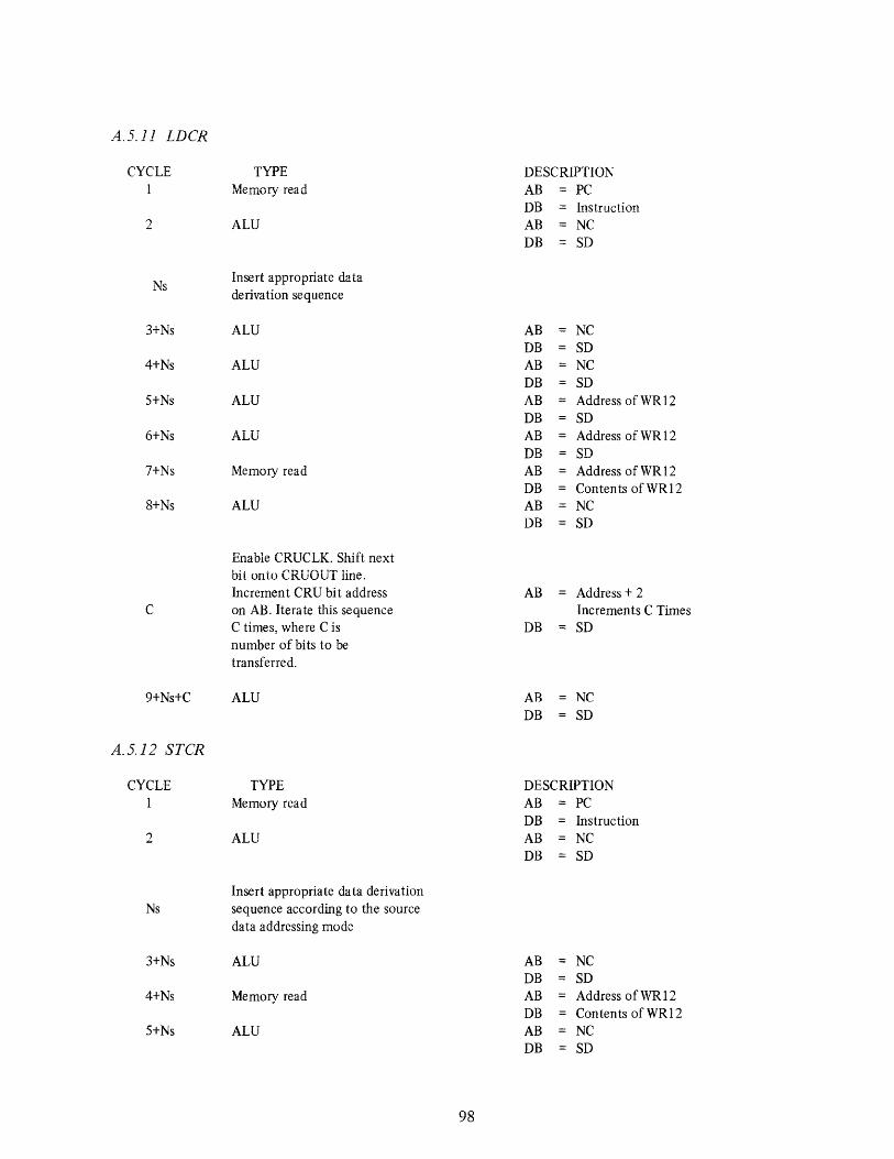
A.5.11 LDCR
CYCLE TYPE DESCRIPTION Memory read AB PC
DB Instruction 2 ALU AB NC
DB SD
Ns Insert appropriate data derivation sequence
3+Ns ALU AB NC DB SD
4+Ns ALU AB NC DB SD
5+Ns ALU AB Address ofWR12 DB SD
6+Ns ALU AB Address ofWR12 DB SD
7+Ns Memory read AB Address ofWR12 DB Contents ofWR12
8+Ns ALU AB NC DB SD
Enable CRUCLK. Shift next bit onto CRUOUT line. Increment CRU bit address AB Address + 2
C on AB. Iterate this sequence Increments C Times C times, where C is DB SD number of bits to be transferred.
9+Ns+C ALU AB NC DB SD
A.5.12 STCR
CYCLE TYPE DESCRIPTION Memory read AB PC
DB Instruction 2 ALU AB NC
DB SD
Insert appropriate data derivation Ns sequence according to the source
data addressing mode
3+Ns ALU AB NC DB SD
4+Ns Memory read AB Address ofWR12 DB Contents of WR12
5+Ns ALU AB NC DB SD
98

CYCLE 6+Ns
TYPE ALU
Input selected CRU bit. Increment CRU bit address.
C Iterate this sequence C times where C is the number of CRU bits to be input.
7+Ns+C ALU
8+Ns+C ALU
Right adjust (with zero C' fill) byte (if C < 8)
or word (if 8 < C < 16).
C' = 8-C-1 if C :;:;;; 8 = 16-C-1 if < C:;:;;; 16
9+Ns+C+C' ALU
10+Ns+C+C' ALU
l1+Ns+C+C' ALU
12+Ns+C+C' Memory write
DESCRIPTION AB NC DB = SD
AB Address + 2 C times
DB SD
AB NC DB SD AB NC DB SD
AB NC DB SD
AB NC DB SD AB NC DB SD AB Source address DB SD AB Source address DB I/O data
NOTE: For STCR instruction the 16-bit word at the source address is fetched. If the number of CRU bits to be transferred is :;:;;; 8, the CRU data is right justified (with zero fill) in the specified byte of the source word and source data word thus modified is then stored back in memory. If the bits to be transferred is > 8 then the source data fetched is not used. The CRU data in this case is right justified in 16-bit word which is then stored at the source address.
A.S.l3 SBZ, SBD
CYCLE TYPE Memory read
2 ALU
3 ALU
4 Memory read
5 ALU
6 CRU
99
DESCRIPTION AB PC DB Instruction AB NC DB SD AB NC DB SD AB Address of WR 12 DB Contents ofWR12 AB NC DB SD Set CRUOUT = 0 for SBZ
= 1 for SBO Enable CRUCLK

CYCLE TYPE DESCRIPTION AB CRU bit address DB = SD
A.5.14 TB
CYCLE TYPE DESCRIPTION Memory read AB PC
DB Instruction " ALU AB NC k
DB SD 3 ALU AB NC
DB SD 4 Memory read AB Address of WR 12
DB Contents ofWR12 5 ALU AB NC
DB SD 6 CRU Set ST(2) = eRUIN
AB Address of CRU bit DB = SD
A.5.15 JEQ, JGT, JH, JHE, JL, JLE, JLT, JAIP, JiVC, JIvE, JlvO, JOC, lOP
CYCLE
2
3
4
5
TYPE Memory read
ALU
ALU
ALU
ALU
A.5.16 SRA, SLA, SRL, SRC
CYCLE
2
3
4
5
TYPE l1ernory read
ALU
Memory read
ALU
ALU
100
DESCRIPTION AB PC DB Instruction AB DB
NC SD
Skip to cycle #5 if TMS 9900 status satisfies the specified jump condition AB NC DB SD AB NC DB Displacement value AB NC DB SD
DESCRIPTION AB PC DB AB DB AB DB
Instruction NC SD Address of the workspace register Contents of the workspace register
Skip to cycle #9 if C*"O C Shift count AB NC DB SD AB NC DB SD

CYCLE 6
7
g
9
C
9+C
10+C
TYPE Memory read
ALU
ALU
Shi ft the con ten ts of the specified workspace register in the specified direction by the specified number of bits. Set appropriate status bits.
Memory write
ALU
A.5.17 AI. ANDI. ORI
CYCLE
2
3
4
5
6
7
A.5.18 CI
CYCLE
2
3
4
5
TYPE Memory read
ALU
ALU
Memory read
Memory read
ALU
Memory write
TYPE Memory read
ALU
Memory read
ALU
Memory read
101
DESCRIPTION AB Address of WRO DB Con ten ts of WRO AB Source address DB SD AB NC DB SD AB NC DB SD
AB = Address of the workspace register DB = Result Increment PC AB NC DB = SD
DESCRIPTION AB PC DB Instruction AB NC DB SD AB NC DB SO AB Address of workspace register DB Contents of workspace register AB PC+2 DB Immediate operand AB NC DB SO AB Address of workspace register DB Resul t of instructi on
DESCRIPTION AB PC DB Instruction AB DB AB DB AB DB AB DB
NC NC Address of workspace register Contenls of workspace legister NC SD PC+2 Immediate operand

CYCLE TYPE DESCRIPTION 6 ALU AB NC
DB SD 7 ALU AB NC
DB SD
A.5.19 LI
CYCLE TYPE DESCRIPTION Memory read AB PC
DB Instruction 2 ALU AB NC
DB SD 3 ALU AB NC
DB SD 4 Memory read AB PC+2
DB Immediate operand 5 ALU AB Address of workspace register
DB SD 6 Memory write AB Address of workspace register
DB Immediate operand
A.5.20 LWPI
CYCLE TYPE DESCRIPTION Memory read An nl""
fiD r'--
DB Instruction 2 ALU AB NC
DB SD 3 ALU AB NC
DB SD 4 Memory read AB PC+2
DB Immediate operand 5 ALU AB NC
DB SO
A.5.21 LIMI
CYCLE TYPE DESCRIPTION Memory read AB PC
DB Instruction 2 ALU AB NC
DB SD 3 ALU AB NC
DB SO 4 Memory read AB PC+2
D13 Immediate data 5 ALU AB NC
DB SO 6 ALU AB NC
DB SD 7 ALU AB NC
DB SO
102

A.5.22 STWP, STST
CYCLE TYPE DESCRIPTION Memory read AB PC
DB Instruction 2 ALU AB NC
DB SD 3 ALU AB Address of workspace register
DB SD 4 Memory write AB Address of the workspace register
DB TMS 9900 internal register contents (WP or ST)
A.5.23 CKON, CKOF, LREX, RSET
CYCLE TYPE DESCRIPTION Memory read AB PC
DB Instruction 2 ALU AB NC
DB SD 3 ALU AB NC
DB SD 4 CRU Enable CRUCLK
AB External instruction code DB SD
5 ALU AB NC DB SD
6 ALU AB NC DB SD
A.5.24 IDLE
CYCLE TYPE DESCRIPTION Memory read AB PC
DB Instruction 2 ALU AB NC
DB SD 3 ALU AB NC
DB SD 4 CRU Enable CRUCLK
AB Idle code DB SD
5 ALU AB NC DB SD
6 ALU AB NC DB NC
103

A.6 Machine-Cycle Sequences in Response to External Stimuli
A.6.1 RESET
CYCLE TYPE DESCRIPTION 1* ALU AB NC
DB SD 2 ALU AB NC
DB SD 3 ALU AB 0
DB 0 4 Memory read AB 0
DB Workspace pointer 5 ALU AB NC
DB Status 6 Memory write AB Address of WR15
DB Contents of Status register 7 ALU AB NC
DB PC 8 Memory write AB Address of workspace register 14
DB PC+2 9 ALU AB Address of WR13
DB SD 10 Memory write AB Address of workspace register 13
DB WP 11 ALU AB NC
DB SD 12 Memory read AB 2
DB New PC 13 ALU AB NC
DB SD
A.6.2 LOAD
CYCLE TYPE DESCRIPTION 1** ALU AB NC
DB SD 2 Memory read AB FFFC 16
DB Contents of FFFC 16
3 ALU AB NC DB Status
4 Memory wri te AB Address WR 15 DB Contents of status register
5 ALU AB NC DB PC
6 Memory write AB Address of workspace DB PC+2
7 ALU AB Address of WR13 DB SD
8 Memory write AB Address of workspace register 13 DB WP
*Occurs immediately after RESET is released. **Occurs immediately after last clock cycle of preceding instruction.
104

CYCLE TYPE DESCRIPTION 9 ALU AB NC
DB SD 10 Memory Read AB FFFE
DB New PC 11 ALU AB NC
DB SD
A. 6.3 Interrupts
CYCLE TYPE DESCRIPTION 1* ALU AB NC
DB SD 2 Memory read AB Address of interrupt vector
DB WP 3 ALU AB NC
DB Status 4 Memory write AB Address of WR15
DB Status 5 ALU AB NC
DB PC 6 Memory write AB Address of workspace register 14
DB PC+2 7 ALU AB Address of WR13
DB SD 8 Memory write AB Address of workspace register 13
DB WP 9 ALU AB NC
DB SD 10 Memory read AB Address of second word of
interrupt vector DB New PC
11 ALU AB NC DB SD
*Occurs immediately after last clock cycle of preceding instruction
105

A0001188
CRUOUT
CRUCLK
rALUCYCLE -I" ALUCYCLE ·1 I T1 I T2 I , I I
WRITE READ WRITE 'READ ALU INTERNAL ALU INTERNAL RESULT REGISTERSI ALU OPERATION RESULT REGISTERSI ALU OPERATION INTO CONSTANTS INTO CONSTANTS INTERNAL ONTO INTERNAL ONTO
, REG!STERS,ALU
I IINPUT I BUSES
i
I REG!STERS,ALU
I IINPUT I BUSES
I
Figure A-t. ALU Cycle
L CRUCYCLE I CRU CYCLE
I"" OUTPUT ~ I
T2 1 T, , 1 I I Tl I T2 I I
; X-----T"""' -....,....-.J/ X'-----T----I; ;.-----=--X I
! I
I I r\1 f{ I I I I 1 i I I I I
INPUT
I
~
T2 T,
I I I I
CRUIN xxxxxxxxXxxxxXxxxxxi<XXXXv\7XXXXVXXXZZVw.'------r---I I I I ¥ 'T (YY\ I I I I I I I I 1 I I I I I
A4- A 15 -.,-I: X 1 I X I : x~: __ ~_~ A0001189
Figure A-2. CRU Cycle
106

1 1 I
I- I WRITE I
READ --I- .. I I T1 MEMORY CYCLE T2 MEMORY CYCLE
I T1 T2
I I I MEMEN~
I X
Ao -A14 ==x VALID X VALID
I I
DBIN ~ I \ I I
rt-WE \ 1 I 1
I I 1 I READY
\ 1 \ { I I I
\ I CE { I
I I 1 I I
WAIT I
DATA DO - 015 X X AOOO1190
Figure A-3. TMS 9900 Memory Cycle (No Wait States)
107

I ~I. ..I I <ill WRITE READ I I I I I
I
T1 T2 I
T3 I T4 T'j T2 I T3 T4 I I I I I I I I I CKOUT U U U U U U U U U
MEMEN
~ X J
I
A13 ______________ ~I \ ____ --1 \~--
AO-A12 ~ __________________________ ~X~ ___________________________ )( _____ __
DBIN / \
WE \ f \ !
READY /
DO - 07 '=:=J( CPU WRITE DATA X CPU WRITE DATA X INPUT MODE 7 RD \ INPUT MODE 7 RD \ INPUT
A0001191
Figure A-4. TMS 9980A/81 Memory Cycle (No Wait States)
108

TI authorized distributors ALABAMA
Hallmark Electronics P.O. 80x 1133/12051 539-0691
Huntsville, Alabama 35801
ARIZONA
Cramer Arizona 26415 E. Universityll602I263·1112
Phoenix, Arilona 85034
R. V. W .. merford Company 3311 W. Earll/l6021 272·7144
Phoenix, Arizona 85017
CALIFORNIA
Cramer/los Angeles 17201 Daimler St.l17141979·3000
Irvine, California 92705
Cramer/San Diego 8913 Complex Dr:ve. Suite E
17141565·1881 San Diego, California 92123
C(smerlSan Francisco 720 Palomar A_ueI14081 739·3011
Sunnyvale. California 94086
Kierulff Electronics, Inc. 2565 Commerce WayI12131685·5511
Los Angeles, California 90040
Kierulff Electrontcs. Inc. 3969 E. Bayshorel14151 968-6292
Palo Alto, California 94303
Kierulff Electronics, Inc. 8797 Balboa Avenuell714 I 278·2112
San Diego. California 92123
Radio PrOducts Sales. Inc. 350 S. Kellogg Ave .• Suite E
18051 964-6873 Goleta. California 93017
Radio Products Sates, Inc. 1501 S. Hill St.l12131 748·1271 los Angeles. Californja 90015
Radio Products Sales. Inc. 7889 Clairemont Mesa Blvd.ll7141 292·561 I
San Diego. California 921 11
Semiconductor Concepts 21201 Oxnard Streetll2131 884-'560
Woodland Hills, California 91364
T I Supply Company 831 S. Douglas 5t.l12131973·2571
EI Segundo. California 90245
TI Supply Company 776 Palomar A""nuoIl4081 732·5555
Sunnyvale. CalifOf'nia 94086
Tme E'ecnonics 900_, Olive StrootIl2131649-6900
Inglewood. California 90301
Time ElectrontCs 2629 Terminal Blvd.l14151965-8000
Mountainvtew. California 94043
R. \/. Wutherford Company 6921 Son Fernando Rd.ll2131 849·3451
Glendale. California 91201
R. V. Weatherford Company 1550 Bobbin A_/17141633·9633
Anaheim, California 92805
R. V. Weatherford Company 3240 H;II,,;ow 0" .. 114151493·5373
Stanford Indus'rlal Park Palo Alto, California 94304
R. V. Weatherford Company 1095 East 3rd S" ... 117141623·1261
Pomona. California 91766
R. V. Weatherford Company 7872 RavtheonI17141278·7400
San Diego. California 92111
COLORADO
Cramer/Denver 5465 east Evons Placell31131 758·2100
Denver, Colorado 802:n
Kierutff Electromcs 10890 East 47th Av • .l131131371-6500
Denver. emorado 80239
CONNECTICUT
Arrow ElectronICS, Inc 295 Treadwell St.ll2031 248·3801
Hamden, Connechcut 06514
Cramer/Connecticut 35 Dodge Avenuel12031 239·5641 Nonh Haven. Connecticut 06473
Milgray/Connecllcut 378 Boston POSt Roadll2031 795·0714
Orange. Connecticut 06411
FLORIDA
Arrow Electronic'S 1001 N.W. 62nd Sunt, Suite 401
13051 776·7790 Ft. Lauderdale. Flo(Jda 33300
Cramer/EW Orlando 345 N. Graham Ave.l13051894·151 I
Orlando. FlOrida 32814
Cramer lEW Holly ...... ood 41135 North 29.h Ave.1I3051 923-8181
Hollywood, FIoft(ia 33020
Hallmark ElectronICs 7233 Lake Ellenor Or.l13051855-402O
Orlando. F 10Hda 31809
Hall·Mark Electronics 1302 W .. t McNab Rd.l13051 97 I ·9280
Fort Lauderdale, Flortda 33310
GEORGIA
CrametfEW AiliiiHi; 3923 Oakchff Industnal Court
14041448·9050 Atlanla. Georgia 30340
ILLINOIS
Cramer/Chicago 1911 South Busse Rd.ll3121 593·8230
Mr. Prospect. IIhnOls 60056
Newark ElectronICS Corp 500 N. Pulask' Road113121638-4411
ChiCagO, Illinois 60624
Semiconductor Specialists P.O. Bo< 66125
O'Hare Inlernatlonal Airport 13121219·1000
ChlCil90, illinois 60666
TI Supply Companv 2420 E. Oak.onI13121593·7660 Arlington Heights, ""nols 60005
INDIANA
Graham Electronics 133 S. Pennsylvania Street
13171634-8202 Indianapolis, India .... 46204
IOWA
OEECO.lnc. 2500 16th Avenue S.W.l13191 365·7551
Cedar Rapids. Iowa 52406
MARYLAND
Arrow Electronics, Inc. 41101 Benson A ... II2021 737·1700
Baltimore, Maryland 21221
Kterulff Electronics, Inc. 16021 Industrial Drive/l301 I 948'()25O
Gaithersburg, Maryland 20760
MilgraylWashington, Inc. 5405 Lafayono Placell3011 864-1111
Hyansville. Maryland 2078 I
Technico Inc. 9130 Rod Branch RoedIf3011461·2200
Columbia, Maryland 21209
MASSACHUSETTS
Cramer Electronics, Inc. 85 Wolis Ave"..eI16171969-7700
Newton, Massachusetts 02159
Kierulff Electronics, Inc. 13 Fortune A"".l16171667·8331
Bilter;c8. Mas.sachusetts 01821
TI SupplV Company 504 Totten Pond Roadl16HI B90·0510
Watham, Massachusens 02154
MICHIGAN
Nev.erk Electronics. Inc. 20700 Hubbell Ave.l13131967-0600
Detroit. Michtgan 48237
Newark Electronics 3645 Li_n S.E.l16161 241-6881
Wyoming. Michigan 49508
MINNESOTA
Arrow Etectrc-n;cs 9700 Newton Ave. Southll6121 BBB-5522
Bloomington, Minnesota 55431
Cramer/Minnesota 7275 Bush Lake Road1l6121835·781 I
Edina. Minnesota 56435
Semiconductor Spec~ll'Sts 8030 Cedar Ave. 5outhIl6121854·BB41
Minneapolis. Minnesota 55420
MISSOURI
LCOMP-St. LOUIS. Inc 2605 5:>uth Hanley Rd.l13141647·5505
St. louis, Missoon63144
LCOMP -Kansas City, Inc. 2211 River'rom 0",(816) 221·2400
Kansas City, MISSOUri 64120
SemlConduCtOf Specialists 3805 N. Oak TrafficwayI18161452·3900
Kansas City. Missouri 64116
Semiconductor SpecialIsts 1020 Anglum Roadl13141 731·2400
Hazelwood. Missoun 63041
NEW JERSEY
Arrow ElectrOniCS Pleasant Valley Ave.l(6091 235·1900
Moore5tQWn, New Jeney 0805 7
Arrow Electrontcs 285 Midland A.dl201I 797·5800 Saddlebrook. Nev-r Jersey 01662
Cramer/Pennsylvanta 12 Spnngdale RoadI12151923·5950
Cherry HIli, NeVII' Jersey 08003
Cr.,mer/New Jersey 1 Barren AveoulI!!'/f2011 935·5600
Moonadlte, New Jersey 01014
General RadiO Supply Company, Inc. 600 Penn 5t.lI6091964·8560 Camden. New Jersey 08102
Klerulll EleclJonics 5 Industnal OuveH2011935·1120
Rutherford, New Jersey 01070
MllgrayfDeIV'IQre Valley. Inc 1165 Marlkr~s Rd
16091424·1300112151228·2000 Cherry Hill. New Jer~ 08034
TI Supply Company 301 Cen.ral Av • .I1201I 382·6400
Clark, New Jersey 01066
NEW MEXICO
Cramer/New MeXICO 137 Vermont N.E.lI5051 265·5767 Albuquerflue. New MeXICO 87108
A. V. WP.alheriord Company 2425 Alamo S.E.lI5051 842·0863 Albuque-f(~ue, N~ MeJo:lco 81106
NEW YORK
Anow Eleclronlcs, In(: 900 Broad Hollow Rd.l15161694·6800
farm;ngda'e. Nco1At YOik 1 ~ 735
Arrow EleclroOics. Inc Old Rou.e 9119141896·7530
FiShkill, Ne ...... York 12524
Cramer/Rochester 3000 s. W,noon Roadl17161 275-0300
Rochester. New York 14623
Cramer/Syracuse 6716 Joy RoadIl3151437·6671 East Syracuse. New York 13057
Cramer/long Island 29 Os .. Ave.115161 231 ·5600 Hauppage, New York 11787
Milgray ElectronICs Inc 191 Hans. Avenuel15161 546-6000
Freeport, New York 11520
Rochesler Radio SupplV Co., Inc 140 w. Main S • .l17161 454· 7800
Rochesler. Ne ...... York '46'~
NORTH CAROLINA
Cramer/EW Winston-Salem 938 Burke 5t.ll9191 72~711
Winston-Salem, North Carolina 27102
Hallmark Electronics 3000 Industrial Dr.l191918J2-4465
Raleigh, North Caroline 27609
OHIO
Arrow Electron;cs, Inc. 23500 Mercantile Rd.1I2161 464-2000
Cleveland. Ohio 44122
ArrOW' Electronics 3100 Plainfield Rd.ll5131 253·9176
Kettering, Ohio 45432
Cramer/Cleveland 5835 Harper Roed/12161 248-8400
Cleveland. Ohio 44139
ESCO Etectronics Inc. 221 CraneSt.l15131226-1133
Dayton. Ohio 45403
OKLAHOMA
TI Supply Company PO. Box Drawer "T", Admiral Station 12151 E. Skelly Dri .. 119181437-4555
T ul ... Oklahoma 74115
OREGON
Almac·Stroum Electronics P.O. Box 25444
8BBB S.W Canyon Roed/l5031 292·3534 Portland, Oregon 97225
PENNSYLVANIA
Arrow Eleetrontes, Inc. Pleasam Valley Ave.II6091 235-1900
Moorestown, New Jersey 08057
General Radio Supply Co. 600 Penn 5t.lI609I964-8560 Camden, New Jersev 08102
Milgray/Delaware Valley, Inc. 1165 Marlkress Rd.
16091424·1300112151228-2000 Phil •. Cherry HIli, New Jersey 08034
TEXAS
Harrtson EQUipment Company. In<:. 1616 McGowenll7131652-'700
Hounon. Texas 71004
R. V. Weatherford Company 3500 West T. C. Jester Blvd.
17131688-7406 HCM.Kton, Texas 17018
TO 5upply Company 6000 Oenton Dri",,112141 238-6823
Dallas, Texas 75235
TI Supply Company 8600 Commerce Park1l713' 777-601 I
Houston, Texas 77042
UTAH
Standard Supply Company 3424 S. Mainll801 I 486·3371 Salt lake City, Utah 84110
WASHING10N
Almac·St,oum ElectronICS 5811 Soxth Ave. So.ll2061 763·2300
Seattle. Washington 98108
K lerultt E iectronics. Inc. 5940 6th Ave. 50.112061763·1550
Seanle. Washington 98108
WISCONSIN
Arrow ElecTronICS, Inc. 2925 S. l60th SorootI14141782·2801
New Berlin, Wisconsin 53151
SemrconduclOf Speclahsts 10855W .. t Pott., Rd.ll41412571330
Wauwatosa. Wisconsin 53226
AUSTRALIA
Adelaide: A J. Ferguson PlY, lid. Melbourne· A. J. Fer9Json & Co. Pty, LUi.
AUSTRIA
V'en",1 TRANSISTOR Venrlehsqes. mhH. 02221829451
BELGIUM
Brussels AVI·Elec, 2/733 96 00 Deurne· G,edav EleCtronICs. 311251925
CANADA
Caly.ary Canadtan Eleclronics, Ltd 141131287.1800
DownsvIew CESCO Electronics. llu. 14161661·9222
Edmonton: Canadian ElecrroOlcs, LuI 141131452·9393
MOl1lreal CESCO Electronics. Lui. 15141 735·5511
Montreal· Future ElecHOntCS 15141 735·5775
Onawa CESCO Electronics, Ltd 1613: 729·5118
Onawa· Future Electronics 16131232· 7757
Quebe-c CilV CESCO EleclroOlcs, LTd 14181 524·4641
RelCdale F ulure E lectro'l'CS 14161677·7820
Vancouver Canadian EleCIrOOlCS, lId 16041324·7911
Vancouver· Future Electronics 16041261·1335
W,nmpeg: Canadian Eleclronlcs, LIn. 12041947·1321
DENMARK
Helle" TI Supplv. 91 74·00
FINLAND
l-ielsm1o TI Supply. 408 300
FRANCE
Le Plessis Robinson: TISCO. 1~0 23 43 Lagardo: Sol .... 94-27 16 10
Lyon: Radiolex. 78-24 51 72 Lyon: Tokol"". 78-74 3740
Mar.me: Industrielle Electrique, 91-50 52 06
MarseHle: Tekelee. 91-47 22 20 Mell: Fachot. 87-68 88 63
Moylan: TISCO. 76-90 45 74 Montrouge: P.E.P .• 1·7353320
Paris: Pariner, 1-87B 65 55 Paris: Radio Voltaire, 1·35750 11
Renn .. : Tekelec. 99-50 62 35 Rungi" Electronique MS. 1-686 74 25
Roubaix: Ellec. ~70 56 19 S .... r .. : Telteloc. 1-626 02 35
Strasbourg: Electronique MS. 88-32 88 32 Tarnes: Tarbelec. 62-93 1082
GERMANY
Aachen: Schilfers Elektronik., 0241/3 05 53 Berlin: TlSCO.II3()'74 44041
Essen: TISCO 0201·20 916 Frankfurt a.M.: Spoerle Electronic.
061113162031-38 Frankfurt·Grisham: TiSeO, 0611·39 9061
Gottingen: Relron GmbH, 0551/6 40 07 Hamburg: TlSCO. 04()'22 96 478
Hamburg: Walter Kluxen, Q40/2 48 91 Hann""er: TlSCO. 0511·55 6041
Munchon: Coidis GmbH. 0891454306 Munchen: Neumuller GmbH. 089/59 91-1
Munchen: TISCO. ()89.32 50 11 Nurnberg: Celdis GmbH. 0911/10 90 10 Schwieberdingen: Elkose.07150131041 Sprendiingen/FFm: Spoerle Electronic,
0611131604-1 Stuttgard: TlSCO. 0711-54· 7001 Toul"""': Electron. 61-62 82 85 Toulouse: Tekeloc. 61-40 24 90 Toulouse: TISCO. 61·80 64 70
Wuppertal·Elberfekf: H. M. Muller, 0212114260 16
ITALY
801ogna: Lasi. 051/46 78 80 Catama: Thynslor. 095/37 20 45
Firenze: Paoletti Fer .• 055/29 4574 Genova: Pasini Elt., 010/56 1015
Milano: Lasi E It .• 021688 63 68 Napoli: Telelux.0811611133 Padova: IOAC. 049/65 77 21
Roms: Cramer hal~, 06151 J9 387 Rorna: SFERA. 06/839 31 72 Torino Carte1'. 011/59 2512 Torino· FIRET. 011166 6572
Tortareto ltdofTeramo: De Dominicis, 095/372045
JAPAN
Tokyo TI Supply. 402·6171
NETHERLAND5
Amslet'ditm·Schtphol. TI Supply. 020·17 36 36
NEW ZEALAND
AuCkl.,nrl David J. Rll!!"ld (N. lJ Ltd., 492·189
NORWAY
OSlO Ingenioflrma M()rgenslierne & Co, 372940
pueRTO RICO
Cramer Oe Puerlo Rico Subdivision General/f8091 892·2600
Bo. Retrto. San German Puerto A ICO 00753
SOUTH AFRICA
Johannesburg Assoclilled E IeCHOnleS PtV. ltd.
SPAIN
Barcelo",l· Oilltron.c S.A .. 253 24 57
SWEDEN
SiockhoJm A. B Gostij Backstrom, 54 03 90
SWITZERLAND
lunch Fahllmex AG. 01/41 06 10
UNITED KINGDOM
BHmlngham TI Suppl.." (021) 143·5293 Derhy Quarndon EleciroOiCS lid ..
0332·32651 Edonburgh: TI Supply. C0311 229·1481
Enfield· Blueline Eteclronic Components. 01·3666371
Harlow Blueltne EleclrOntC Componenls, 0279·29588
Harlow· Mogul Electronics Ltd., 029·39771
London fSloughl: Anlac Componenn ltd .. 0753·35446
London ISloughl TI Supply. 0753·3341 I PortsmOUTh· 50S Components Lid.,
0705-65311 Southampton TI Supply, 0703·21741 Stockpo,. TI SuppiV. 061-432 0645

,/
TI "'orld\Vide sales offices ALABAMA
4717 University Drive, Suite 101 Huntsville, Alabama 35805
205-837-7530
ARIZONA
P.O. Box 35160 8102 N 23rd Ave_, Suite A
Phoenix, Arizona 85069 602-249-1313
CALIFORNIA
3186J Airway Costa Mesa, California 92626
714-540-7311
831 S. Douglas St. Ei Segundo, Caiiiornia 90245
213-973-2571
7827 Convoy Ct., Suite 412 San Diego, California 92111
714-279-2622
P.O. Box 9064 776 Palomar· Avenue
Sunnyvale, California 94086 408-732-1840
COLORADO
9725 E. Hampden St., Suite 301 Denver, Colorado 80231
303-751-1780
CONNECTICUT
2405 Whitney Avenue Hamden, Connecticut 06518
203-281-0074
FLORIDA
4600 West Commercial Blvd. Fort Lauderdale, Florida 33319
305-733-3300
1850 Lee Road, Suite 115 Winter Park, Florida 32789
305-644-3535
ARGENTINA
Texas Instruments Argentina S.A.I.C.F.
Km. 25, 5 Ruta Panamencana Don Torcuato C.C. Box 2296 - Correo Central
Buenos Aires, Argentina
MP 702
748-1141
ASIA
Texas Instruments Asia Ltd
Aoyama Tower Bldg. 4,5, & 6F
24-15 Minami Aoyama 2-Chome, Minato-Ku,
Tokyo, Japan 107 03-402-6171
902, Asian House 1 , Hennessy Road
Hong Kong 51279041
Room 507, Chia Hsin Bldg. 96 Chung Shan North Road, Sec. 2
Taipei, Taiwan
P.O. Box 2093 990 Bendemeer Rd.
Singapore 1, RepubliC of Singapore
AUSTRALIA
Texas Instruments Australia Ltd.
Unit 1 A, 9 Byfield Street, P.O Box 106 North Ryde, N.S.W. 2113
Sydney, A",,"alia 887.1122
AUSTRIA
Texas Instruments Ges. M.B.H.
Rennweg 17 1030 Wien, Austria
724-186
BELGIUM
Texas Instruments Belgium SA
A'venue EdoiJCird LoCCnYlbie 2i B-1040 Brussels, Belgium
733-9623
ILLINOIS
515 W. Algonquin Arlington Heights, Illinois 60005
312-640-3000
INDIANA
2020 Inwood Drive Ft. Wayne, Indiana 46805
219-424-5174
2346 S. Lynhurst Dr., Suite 101 Indianapolis, Indiana 46241
317-248-8555
MARYLAND
6024 Jamina Downs Columbia, Maryland 21045
301-997-4755
MASSACHUSETTS
504 Totten Pond Road Waltham, Mass. 02154
617-890-7400
MICHIGAN
Central Park Plaza 26211 Central Park Blvd., Suite 215
Southfield, Michigan 48076 313-353-0830
MINNESOTA
A.I.C. Bldg., Suite 202 7615 Metro Blvd.
Edina, Minn. 55435 612-835-2900
MISSOURI
8080 Ward Parkway Kansas City, Missouri 64114
816-523-2500
NEW JERSEY
1245 Westfield Ave. Clark, New Jersey 07066
201-574-9800
BRAZIL
Texas Instrumentos Electronlcos do Brasil Ltda.
Rua Padre Pereira Andrade, 591 05469 Sao Paulo, SP, BraSil
260-6347 & 260-5710
CANADA
Texas Instruments Incorporated
945 McCaffery Street St. Laurent H4Tl N3
Quebec, Canaoa 514-341-3232
280 Centre Str. East Richmond Hill (Toronto)
Ontario, Canada 416-889-73 73
DENMARK
Texas Instruments AIS
ManelundveJ 46 D OK-2730 Herlev, Denmark
917400
FINLAND
Texas Instruments Finland OY
F reesen katu 6 P.O. Box 917
00101 Helsinki 10, Finland 408300
FRANCE
Texas Instruments France
L-.:. B0u'~IJIt:'I~. B~u(,; A. R.N. 186 92350 Le PlesSIS Robinson, France
(1) 6302343
31, Qual Rambaud 69002 Lvon, France
(8) 373585
9, Place de Bretange 35000 Rennes, France
(99) 795481
L'Autan 100, Aile de Barcelone 31500 Toulouse, France
(61) 21 3032
i I Av. de ia Chartreuse 3824C Meylan, France
(76) 90 4574
NEW MEXICO
1101 Cardenas Drive, N.E., Room 215
Albuquerque, New Mexico 871 10 505-265-6491
NEW YORK
6700 Old Collamer Rd. East Syracuse, New York 13057
315-463-9291
112 Nanticoke Ave., P.O. Box 618 Endicott, New York 13760
607-754-3900
201 Sout!"l Avenue Poughkeepsie, New York 12601
914-473-2900
1210 Jefferson Rd. Rochester, New York 14623
716-461-1800
1 Huntington Quadrangle, Suite 1 COl Melville, New York 11746
516-293-2560
NORTH CAROLINA
1 Woodlawn Green, Woodlawn Road Charlotte, North Carolina 28210
704-527-0930
OHIO
Belmont Bldg., Suite 120 28790 Chagrin Blvd.
Cleveland, Ohio 44122 216-464-2990
Hawley Bldg., Suite 101 4140 Linden Avenue Dayton, Ohio 45432
513-253-3121
GERMANY
Texas Instruments Deutschland GmbH.
Haggertystrasse 1 8050 Freising, Germany
08161180-1
Frankfurter Ring 243 8000 Munich 40, Germany
089/325011-15
Lazarettstrasse 19 4300 Essen, Germany
0201/233551
AkaZienstrasse 22-26 6230 Frankfurt-Griesheim, Germany
0611/399061
Riethorst 4 3000 Hannover 51, Germany
0511164 80 21
Krefelderstrasse 11-15 7000 Stuttgart 50, Germany
0711154 7001
Kudueistendamm 146 1000 Berlin, Germany
030/89 27 063
ITALY
Texas Instruments Italia SpA
Via Della Glustllia 9 20125 MoIan, Italy
02-688 3141
Vl~ t. Pv1~nCIr:el!2 65 00199 Roma, Italy
06-837745
Via Montebello 27 10124 Torino, Italy
011-83 22 76
MEXICO
Texas Instruments de MeXICO S.A.
Poniente 116 #489 Industrial ValleJO
MeXICO City, 15, D.F., Mexico 567-92-00
OREGON
10700 S.W. Beaverton Hwy, Suite 11
Beaverton, Oregon 97005 503-643-6759
PENNSYLVANIA
275 Commerce Drive, Suite 300 Fort Washington, Pa. 19034
215-643-6450
TEXAS
6000 Denton Drive P.O. Box 5012, MIS 366
Dallas, Texas 75222 214-238-6805
8600 Commerce Park Drive Houston, Texas 77036
713-776-6511
VIRGINIA
Crystal Square 4 1745 Jefferson Davis Hwy., Suite 600
Arlington, Virginia 22202 703-979-9650
3930 Beuiah Rd. Richmond, Virginia 23234
804-275-8148
WASHINGTON
'700 112th N.E., SUite 10 Bellevue, Washington 98004
206-455-3480
NETHERLANDS
Texas Instruments Holland B.V.
Laan Van de Helende Meesters No. 421 Arnstelveen, Holland
473391
NORWAY
Texas Instruments Norway AIS
Rye!"'!5V!!'"!gen 15 Oslo 6, Norway (02) 68 94 85
PORTUGAL
Texas Instruments Equipamento Electronico LDA
Rua Eng. F rede"co Ulrich 2650
Moreira Da Mala. Portugal 94811003
SPAIN
Texas Instruments Espana S.A.
Calle Mallorca 272-276 12 Barcelona 12, Spain
2152950
SWEDEN
Texas Instruments International Trade Corporation (Sverigefilialen)
Fack Nona Hannvagen 3
S - 100 54 Stockholm Sweden
08-235480
UNITED KINGDOM
Texas Instruments Limited
Manton Lane Bedford, England
0234-67466
Printed in U .S,A.