Embed Size (px)
Citation preview
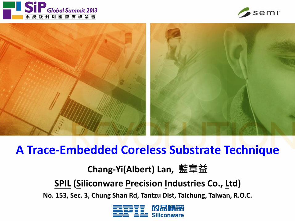
A Trace-Embedded Coreless Substrate Technique
Chang-Yi(Albert) Lan, 藍章益
SPIL (Siliconware Precision Industries Co., Ltd) No. 153, Sec. 3, Chung Shan Rd, Tantzu Dist, Taichung, Taiwan, R.O.C.
Outline
• Introduction of Embedded Technology
• Package Features & KEY Drivers
• Challenges & its Solutions
• Future Developing Roadmap
• Conclusions
Outline
• Introduction of Embedded Technology
• Package Features & KEY Drivers
• Challenges & its Solutions
• Future Developing Roadmap
• Conclusions
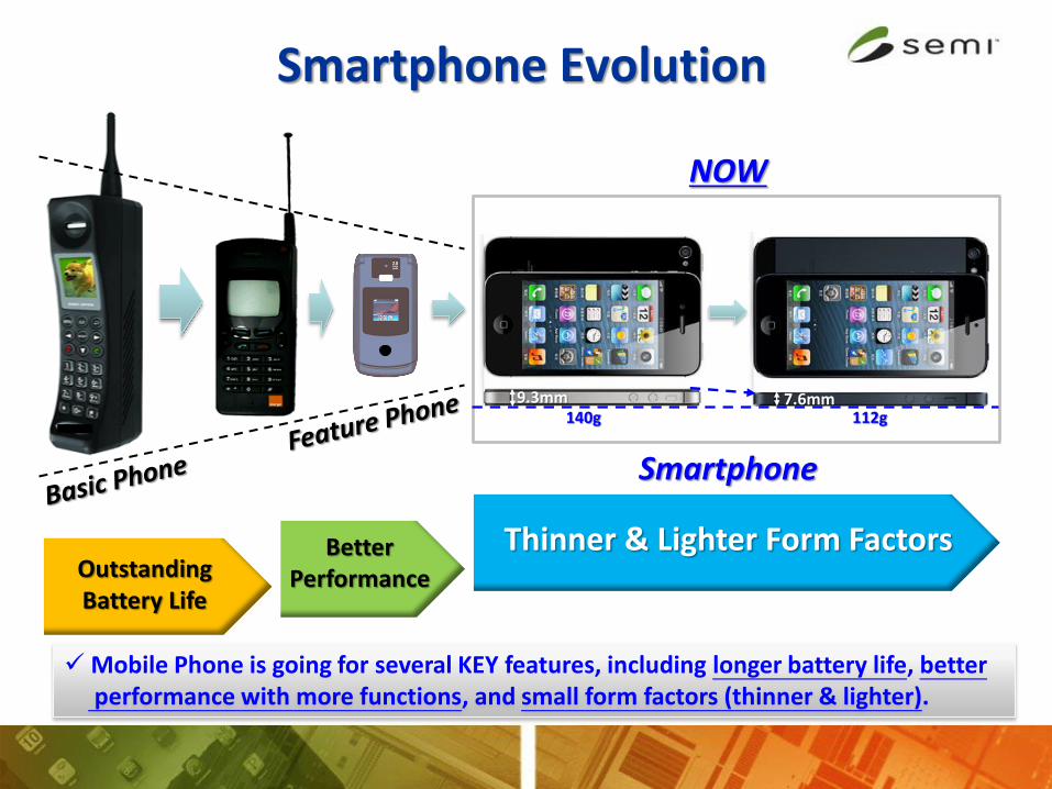
NOW
Thinner & Lighter Form Factors Outstanding Battery Life
Better Performance
Smartphone Evolution
Smartphone
9.3mm 7.6mm 140g 112g
Mobile Phone is going for several KEY features, including longer battery life, better performance with more functions, and small form factors (thinner & lighter).
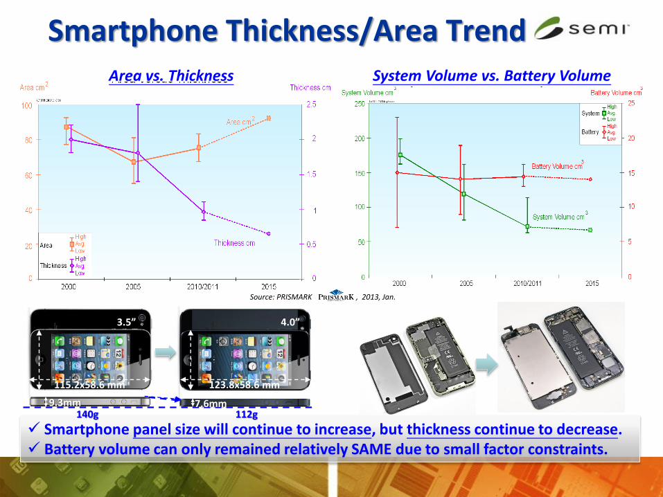
Smartphone panel size will continue to increase, but thickness continue to decrease. Battery volume can only remained relatively SAME due to small factor constraints.
9.3mm 7.6mm 140g 112g
System Volume vs. Battery Volume Area vs. Thickness
Smartphone Thickness/Area Trend
Source: PRISMARK , 2013, Jan.
115.2x58.6 mm 123.8x58.6 mm
3.5” 4.0”
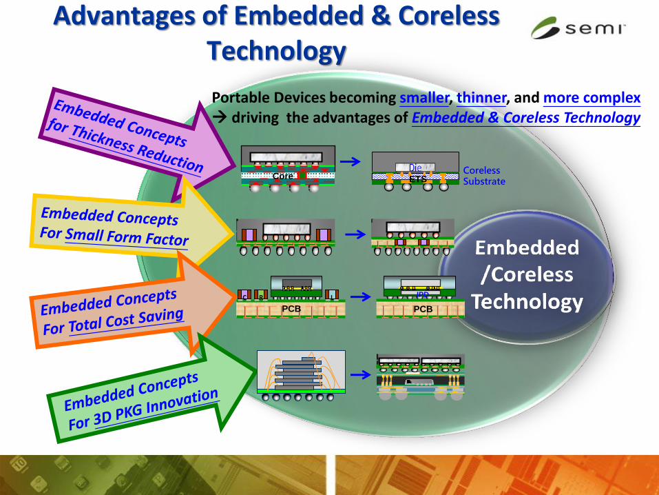
Advantages of Embedded & Coreless Technology
Portable Devices becoming smaller, thinner, and more complex driving the advantages of Embedded & Coreless Technology
PCB
C R L
PCB
IPD
Core ETS Coreless Substrate
Embedded Technology
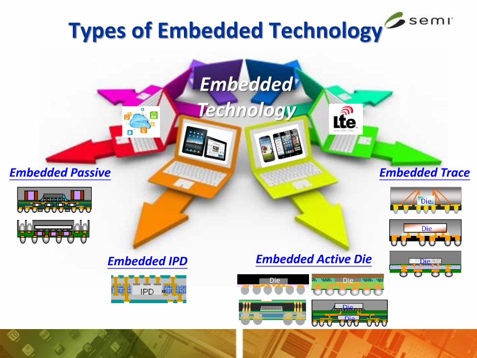
Types of Embedded Technology
Embedded Passive
Embedded Active Die
Die Die
Embedded IPD
Embedded Trace
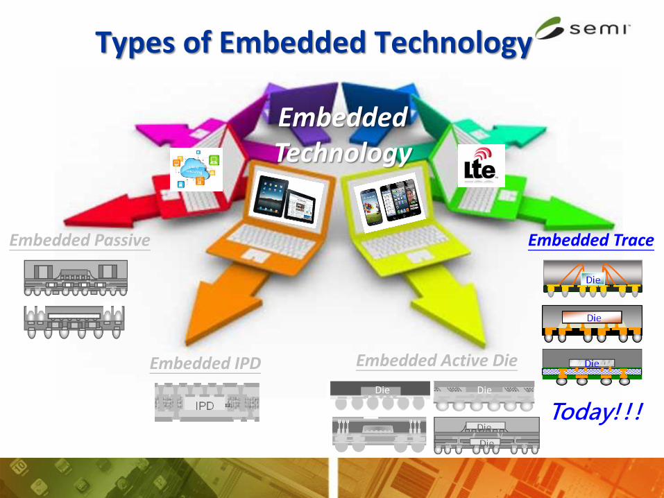
Embedded Technology
Types of Embedded Technology
Embedded Passive
Embedded Active Die
Die Die
Embedded IPD
Embedded Trace
Today!!!
4
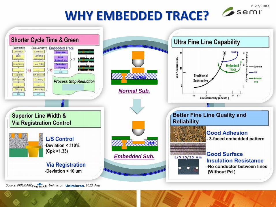
Source: PRISMARK , Unimicron , 2013, Aug.
WHY EMBEDDED TRACE? 612.3/018KK
CORE
Normal Sub.
Embedded Sub.
PP
Outline
• Introduction of Embedded Technology
• Package Features & KEY Drivers
• Challenges & its Solutions
• Future Developing Roadmap
• Conclusions
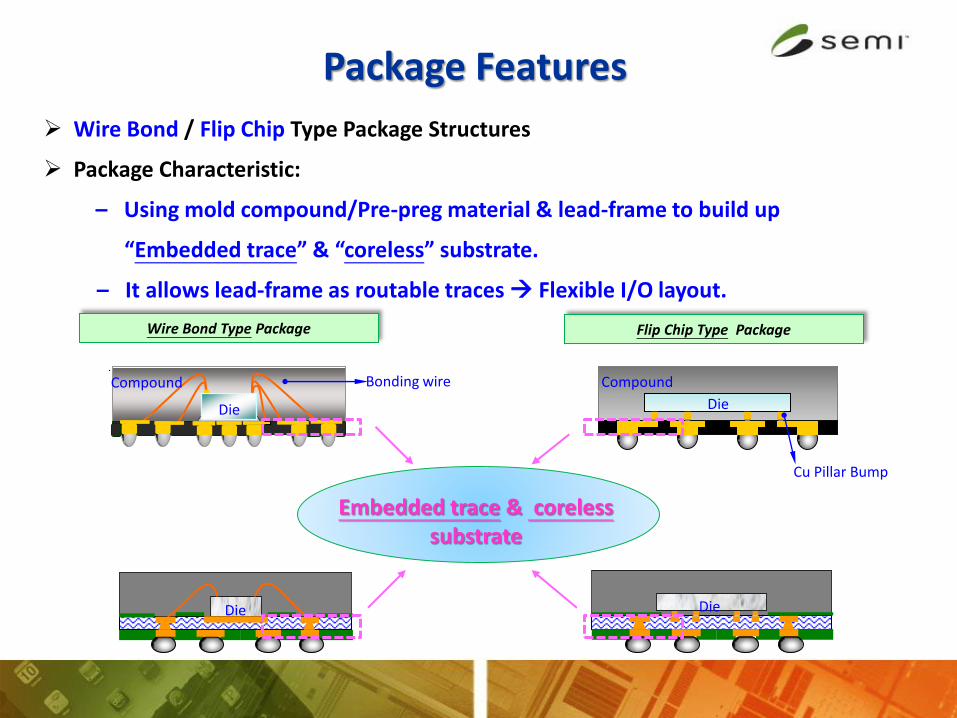
Wire Bond / Flip Chip Type Package Structures
Package Characteristic:
– Using mold compound/Pre-preg material & lead-frame to build up
“Embedded trace” & “coreless” substrate.
– It allows lead-frame as routable traces Flexible I/O layout.
Wire Bond Type Package Flip Chip Type Package
Die
Bonding wire Compound
Package Features
Embedded trace & coreless substrate
Cu Pillar Bump
Die
Compound
Die
Die

Shrink PKG size by Design
– Design capability can shrink package size for low cost and small form factor
128 IO : TQFP 14X14 10x10 ( Due to Routable Trace)
256 IO : LQFP 24X24 12X12 or 13x13
– Flexible I/O layout and package outline as same as TFBGA.
TQFP 128, 14x14 DR-QFN 128, 12x12 Embedded Trace
128, 10x10
Product Drivers
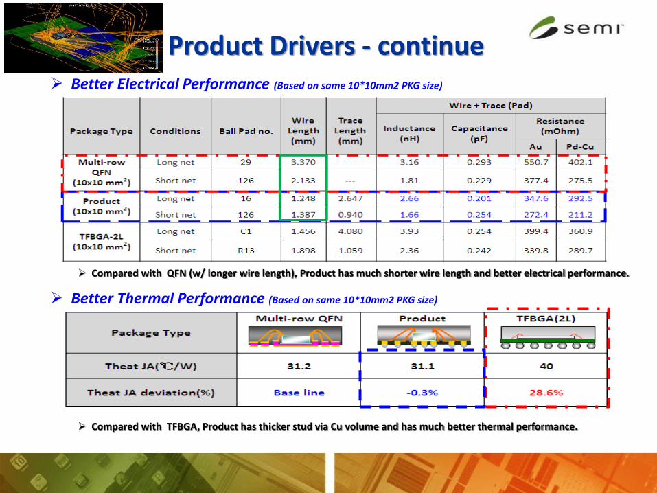
Better Electrical Performance (Based on same 10*10mm2 PKG size)
Better Thermal Performance (Based on same 10*10mm2 PKG size)
Compared with QFN (w/ longer wire length), Product has much shorter wire length and better electrical performance.
Compared with TFBGA, Product has thicker stud via Cu volume and has much better thermal performance.
Product Drivers - continue
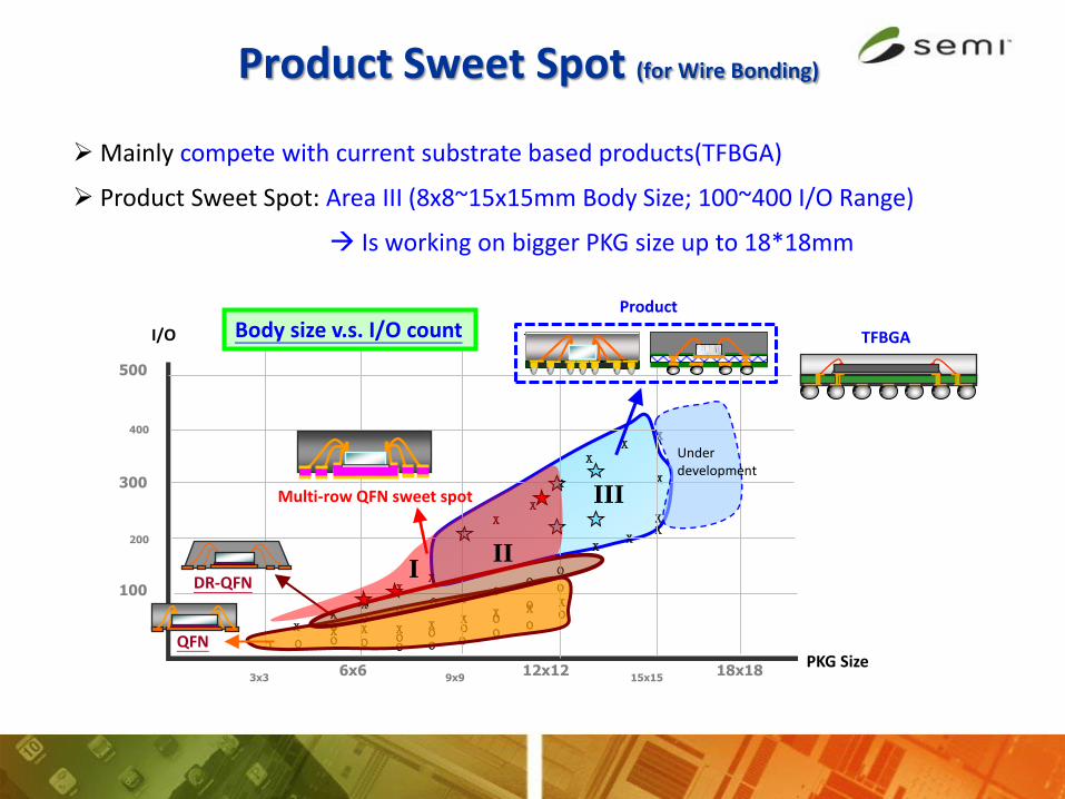
Product Sweet Spot (for Wire Bonding)
Mainly compete with current substrate based products(TFBGA)
Product Sweet Spot: Area III (8x8~15x15mm Body Size; 100~400 I/O Range)
Is working on bigger PKG size up to 18*18mm
PKG Size
I/O
100
200
300
6x6 12x12 18x18 3x3 9x9 15x15
400
500
x x x x x x x x
x x
x
x
x
x x
x x
x x
x
x x
x x
o o o x
o
o o
o
o o o
o o
o o o o
o
o o
o o
o o
o
Multi-row QFN sweet spot
DR-QFN
Body size v.s. I/O count Product
QFN
Under development
TFBGA
III
II I
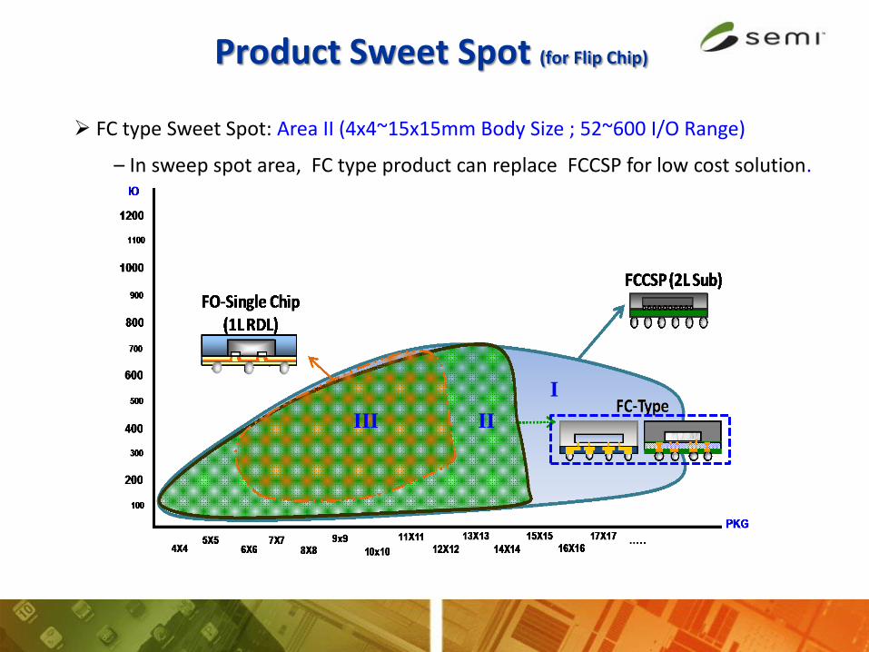
FC type Sweet Spot: Area II (4x4~15x15mm Body Size ; 52~600 I/O Range)
– In sweep spot area, FC type product can replace FCCSP for low cost solution.
III II
I
Product Sweet Spot (for Flip Chip)
Outline
• Introduction of Embedded Technology
• Package Features & KEY Drivers
• Challenges & its Solutions
• Future Developing Roadmap
• Conclusions
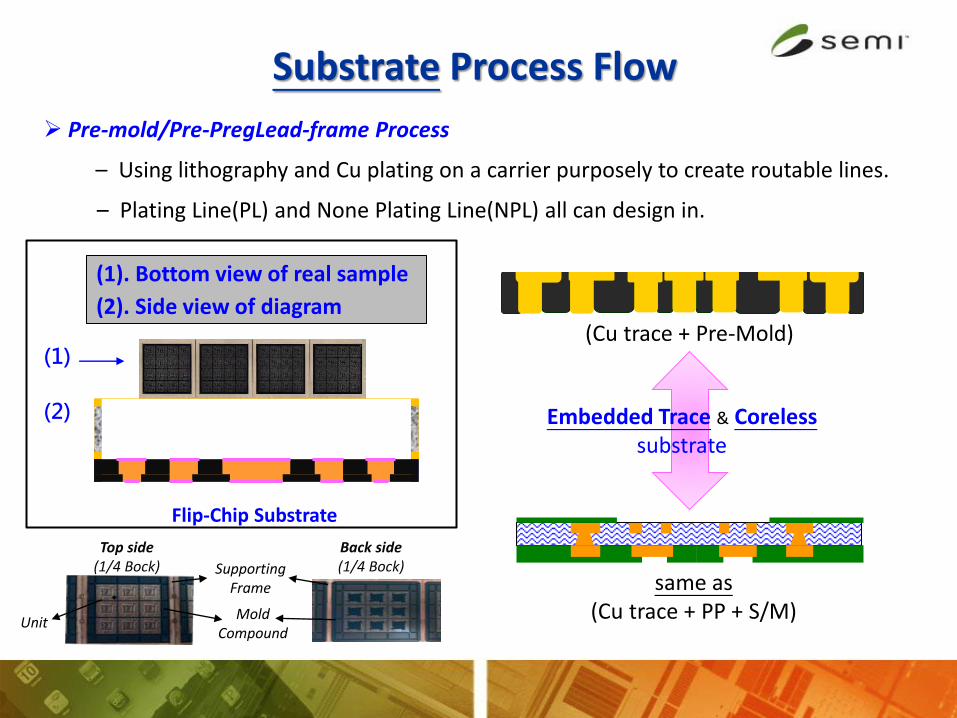
Flip-Chip Substrate
(1)
(2)
Metal Carrier Pre-treatment
(Cu plating) Image transfer (For top trace)
Cu plating (1st layer)
Image transfer (For ball pad)
Cu plating (2nd Cu layer)
Dry Film Stripping Molding Window Etching and OSP coating
(1). Bottom view of real sample
(2). Side view of diagram
Pre-mold/Pre-PregLead-frame Process
– Using lithography and Cu plating on a carrier purposely to create routable lines.
– Plating Line(PL) and None Plating Line(NPL) all can design in.
Substrate Process Flow
(Cu trace + Pre-Mold)
same as (Cu trace + PP + S/M)
Embedded Trace & Coreless substrate
Supporting Frame
Mold Compound
Unit
Top side (1/4 Bock)
Back side (1/4 Bock)
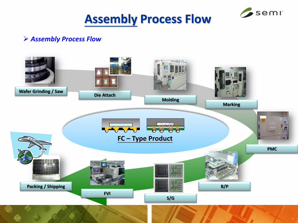
Assembly Process Flow
Assembly Process Flow
FC – Type Product
Wafer Grinding / Saw Die Attach
PMC
B/P
S/G FVI
Packing / Shipping
Molding Marking
Confidential
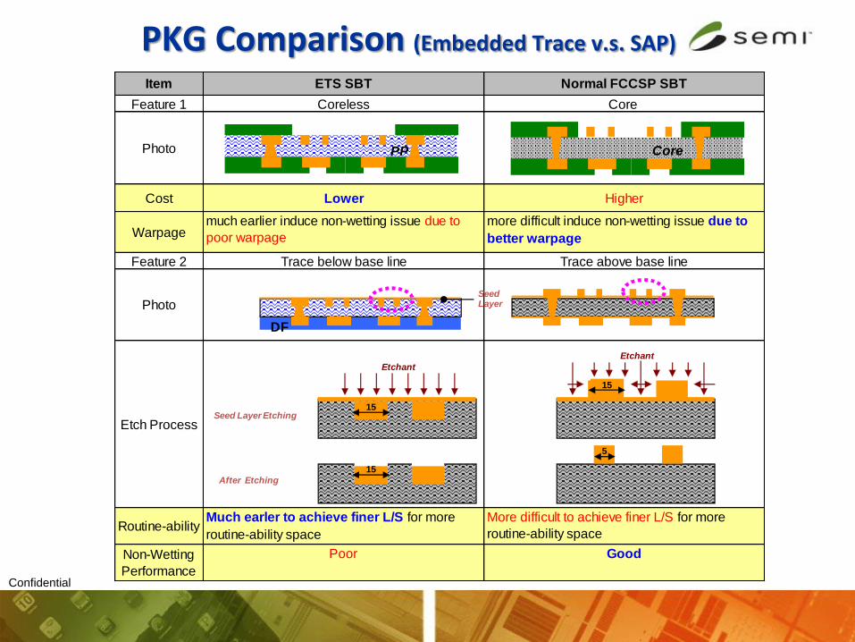
PKG Comparison (Embedded Trace v.s. SAP)
ETS SBT Normal FCCSP SBT
Coreless Core
Lower Higher
much earlier induce non-wetting issue due to
poor warpage
more difficult induce non-wetting issue due to
better warpage
Trace below base line Trace above base line
Much earler to achieve finer L/S for more
routine-ability space
More difficult to achieve finer L/S for more
routine-ability space
Poor GoodNon-Wetting
Performance
Etch Process
Routine-ability
Photo
Item
Feature 1
Photo
Feature 2
Warpage
Cost
DF
Seed Layer
Seed Layer Etching
After Etching
Etchant
Etchant
15
15
15
5
PP Core
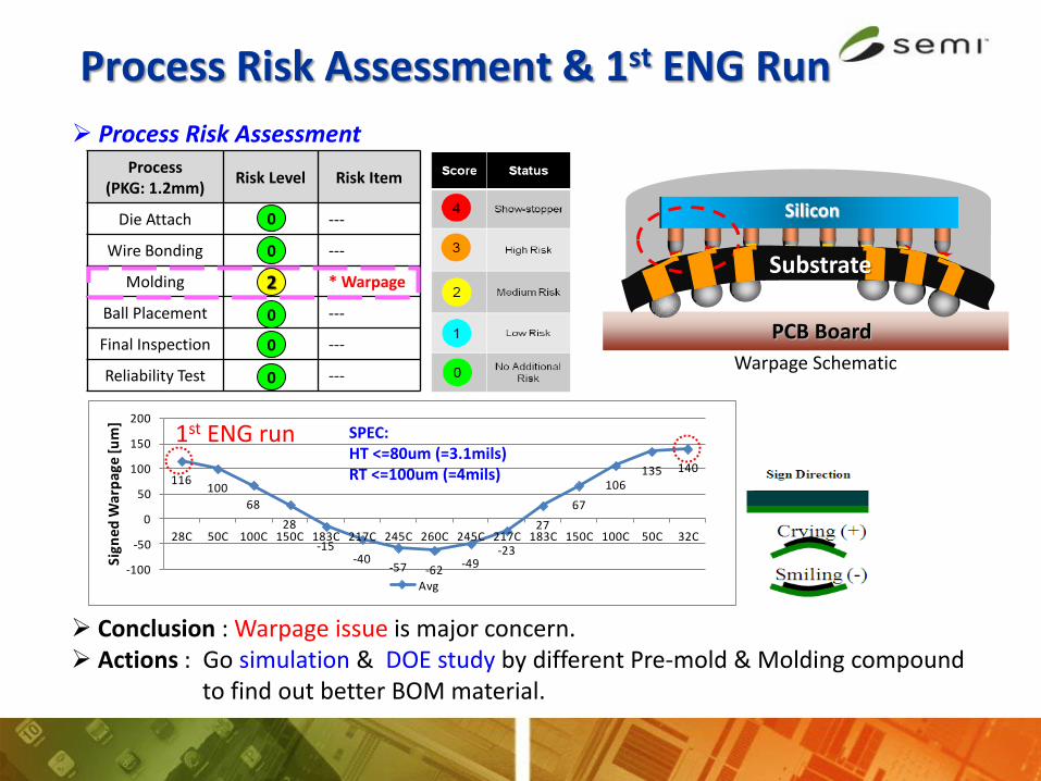
Process (PKG: 1.2mm)
Risk Level Risk Item
Die Attach ---
Wire Bonding ---
Molding * Warpage
Ball Placement ---
Final Inspection ---
Reliability Test ---
0
Process Risk Assessment & 1st ENG Run
Process Risk Assessment
Conclusion : Warpage issue is major concern. Actions : Go simulation & DOE study by different Pre-mold & Molding compound to find out better BOM material.
0
2
0
0
0 PCB Board
Warpage Schematic
Silicon
Substrate
116100
68
28
-15-40
-57 -62-49
-23
27
67
106135 140
-100
-50
0
50
100
150
200
28C 50C 100C 150C 183C 217C 245C 260C 245C 217C 183C 150C 100C 50C 32C
Sign
ed
War
pag
e [
um
]
Avg
SPEC: HT <=80um (=3.1mils) RT <=100um (=4mils)
1st ENG run
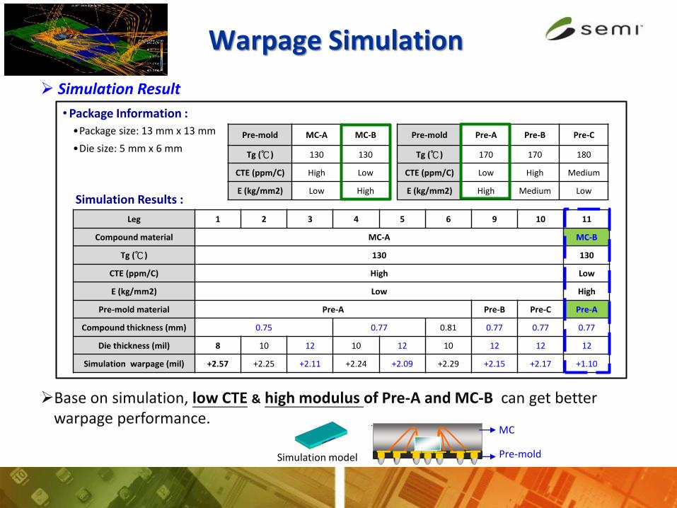
Warpage Simulation
Simulation Result
Simulation Results :
•Package Information :
•Package size: 13 mm x 13 mm
•Die size: 5 mm x 6 mm
Leg 1 2 3 4 5 6 9 10 11
Compound material MC-A MC-B
Tg (℃) 130 130
CTE (ppm/C) High Low
E (kg/mm2) Low High
Pre-mold material Pre-A Pre-B Pre-C Pre-A
Compound thickness (mm) 0.75 0.77 0.81 0.77 0.77 0.77
Die thickness (mil) 8 10 12 10 12 10 12 12 12
Simulation warpage (mil) +2.57 +2.25 +2.11 +2.24 +2.09 +2.29 +2.15 +2.17 +1.10
Pre-mold Pre-A Pre-B Pre-C
Tg (℃) 170 170 180
CTE (ppm/C) Low High Medium
E (kg/mm2) High Medium Low
Base on simulation, low CTE & high modulus of Pre-A and MC-B can get better warpage performance.
Simulation model
Pre-mold MC-A MC-B
Tg (℃) 130 130
CTE (ppm/C) High Low
E (kg/mm2) Low High
MC
Pre-mold
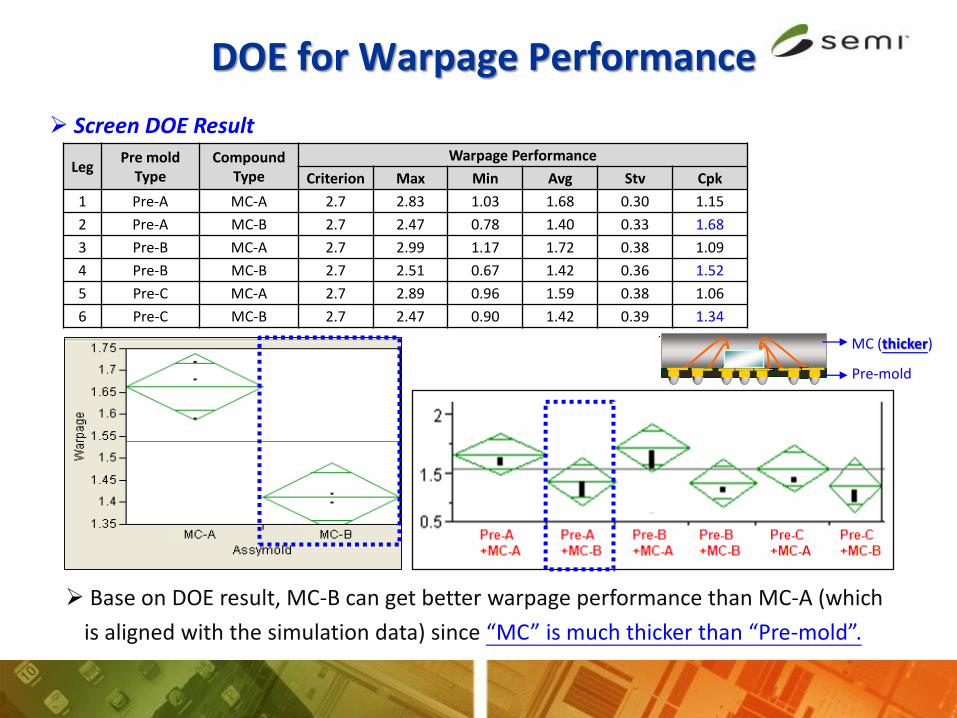
DOE for Warpage Performance
Screen DOE Result
Leg Pre mold
Type Compound
Type
Warpage Performance
Criterion Max Min Avg Stv Cpk
1 Pre-A MC-A 2.7 2.83 1.03 1.68 0.30 1.15
2 Pre-A MC-B 2.7 2.47 0.78 1.40 0.33 1.68
3 Pre-B MC-A 2.7 2.99 1.17 1.72 0.38 1.09
4 Pre-B MC-B 2.7 2.51 0.67 1.42 0.36 1.52
5 Pre-C MC-A 2.7 2.89 0.96 1.59 0.38 1.06
6 Pre-C MC-B 2.7 2.47 0.90 1.42 0.39 1.34
Base on DOE result, MC-B can get better warpage performance than MC-A (which
is aligned with the simulation data) since “MC” is much thicker than “Pre-mold”.
MC (thicker)
Pre-mold
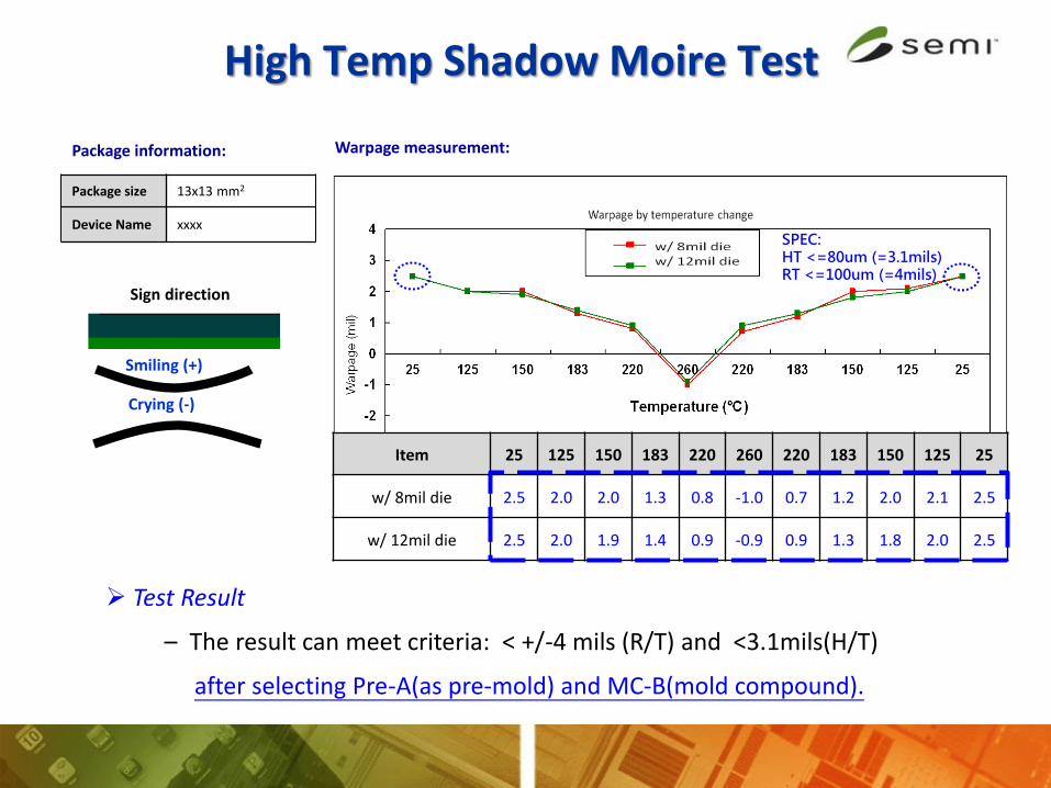
Item 25 125 150 183 220 260 220 183 150 125 25
w/ 8mil die 2.5 2.0 2.0 1.3 0.8 -1.0 0.7 1.2 2.0 2.1 2.5
w/ 12mil die 2.5 2.0 1.9 1.4 0.9 -0.9 0.9 1.3 1.8 2.0 2.5
Crying (-)
Smiling (+)
Sign direction
Package information:
Package size 13x13 mm2
Device Name xxxx
Warpage measurement:
Test Result
– The result can meet criteria: < +/-4 mils (R/T) and <3.1mils(H/T)
after selecting Pre-A(as pre-mold) and MC-B(mold compound).
High Temp Shadow Moire Test
SPEC: HT <=80um (=3.1mils) RT <=100um (=4mils)
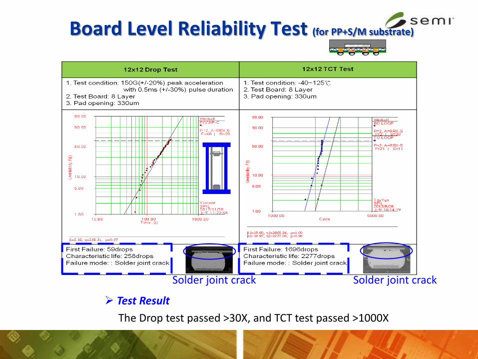
Board Level Reliability Test (for PP+S/M substrate)
Solder joint crack Solder joint crack
Test Result
The Drop test passed >30X, and TCT test passed >1000X
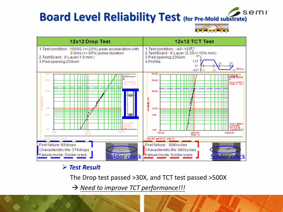
Board Level Reliability Test (for Pre-Mold substrate)
Solder crack
Test Result
The Drop test passed >30X, and TCT test passed >500X
Need to improve TCT performance!!!
Solder crack
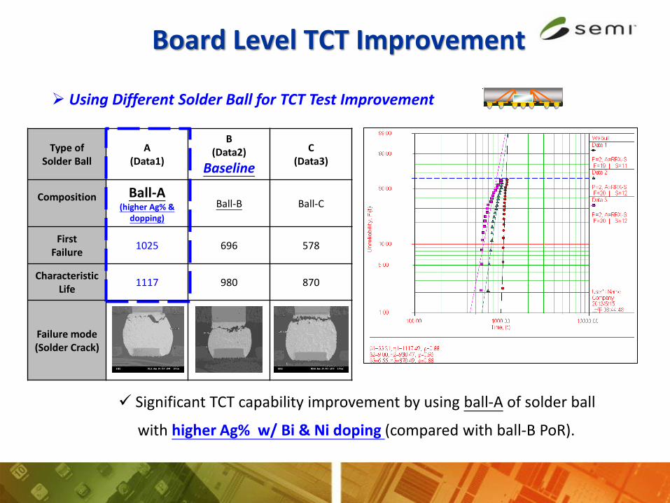
Board Level TCT Improvement
Using Different Solder Ball for TCT Test Improvement
Type of Solder Ball
A (Data1)
B (Data2)
Baseline
C (Data3)
Composition
Ball-A (higher Ag% &
dopping)
Ball-B Ball-C
First Failure
1025 696 578
Characteristic Life
1117 980 870
Failure mode (Solder Crack)
Significant TCT capability improvement by using ball-A of solder ball
with higher Ag% w/ Bi & Ni doping (compared with ball-B PoR).
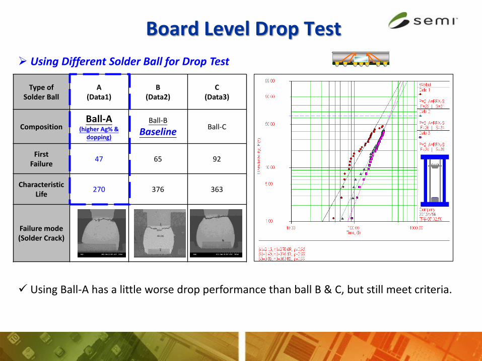
Board Level Drop Test
Using Different Solder Ball for Drop Test
Type of Solder Ball
A (Data1)
B (Data2)
C (Data3)
Composition Ball-A
(higher Ag% & dopping)
Ball-B
Baseline Ball-C
First Failure
47 65 92
Characteristic Life
270 376 363
Failure mode (Solder Crack)
Using Ball-A has a little worse drop performance than ball B & C, but still meet criteria.
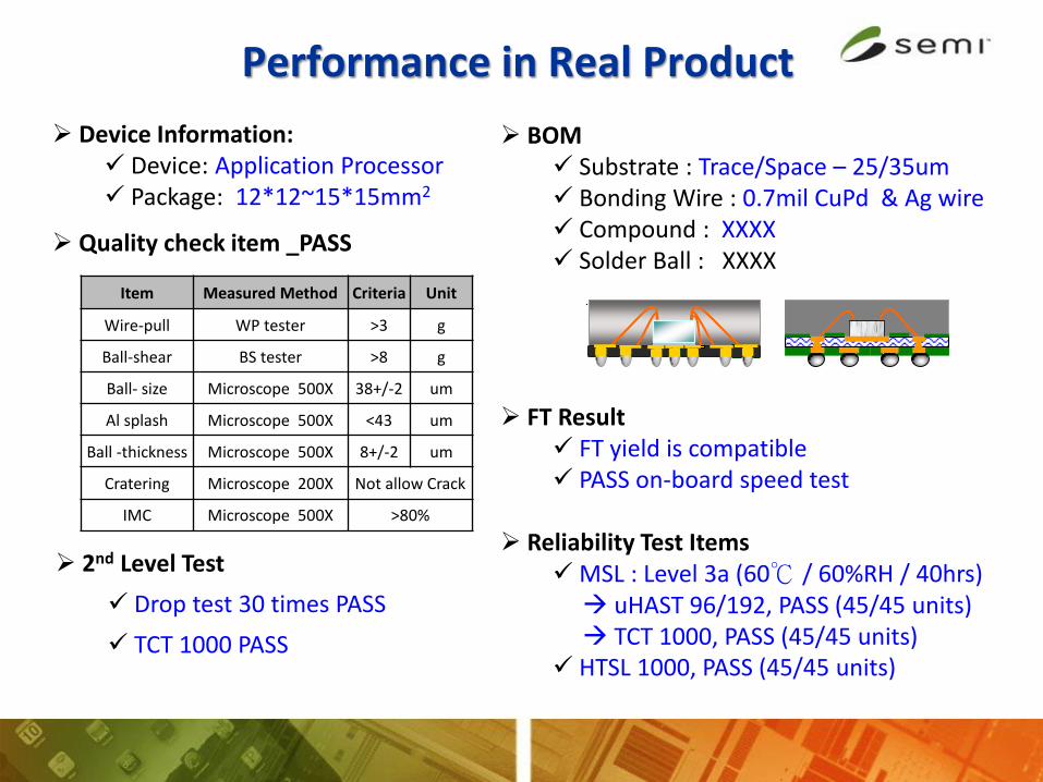
Performance in Real Product
Device Information: Device: Application Processor Package: 12*12~15*15mm2
Quality check item _PASS
Item Measured Method Criteria Unit
Wire-pull WP tester >3 g
Ball-shear BS tester >8 g
Ball- size Microscope 500X 38+/-2 um
Al splash Microscope 500X <43 um
Ball -thickness Microscope 500X 8+/-2 um
Cratering Microscope 200X Not allow Crack
IMC Microscope 500X >80%
2nd Level Test
Drop test 30 times PASS
TCT 1000 PASS
BOM Substrate : Trace/Space – 25/35um Bonding Wire : 0.7mil CuPd & Ag wire Compound : XXXX Solder Ball : XXXX
FT Result
FT yield is compatible PASS on-board speed test
Reliability Test Items
MSL : Level 3a (60℃ / 60%RH / 40hrs) uHAST 96/192, PASS (45/45 units) TCT 1000, PASS (45/45 units) HTSL 1000, PASS (45/45 units)
Outline
• Introduction of Embedded Technology
• Package Features & KEY Drivers
• Challenges & its Solutions
• Future Developing Roadmap
• Conclusions
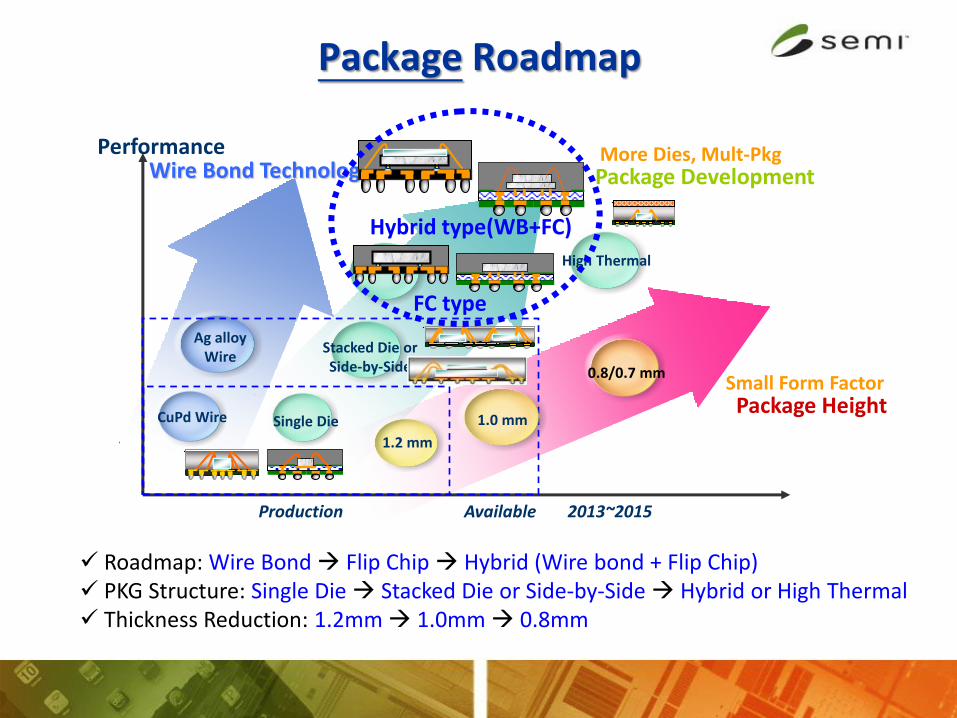
Package Roadmap
Roadmap: Wire Bond Flip Chip Hybrid (Wire bond + Flip Chip) PKG Structure: Single Die Stacked Die or Side-by-Side Hybrid or High Thermal Thickness Reduction: 1.2mm 1.0mm 0.8mm
Package Development Wire Bond Technology Performance
2013~2015 Production
CuPd Wire
Ag alloy Wire
Package Height
0.8/0.7 mm
1.0 mm
1.2 mm
Single Die
Stacked Die or Side-by-Side
More Dies, Mult-Pkg
Small Form Factor
Available
Hybrid type(WB+FC)
High Thermal
FC type
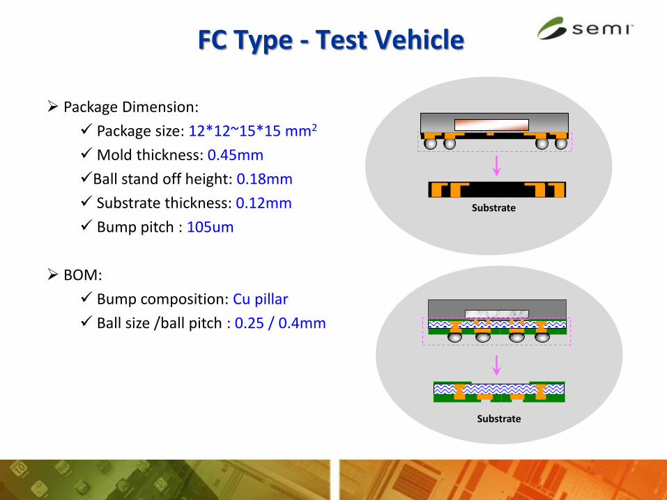
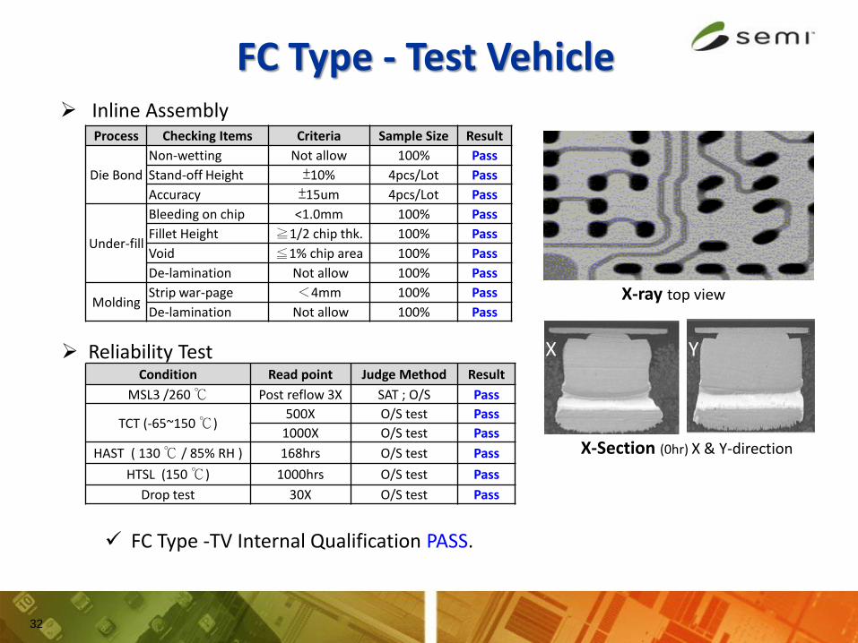
FC Type - Test Vehicle
Package Dimension:
Package size: 12*12~15*15 mm2
Mold thickness: 0.45mm
Ball stand off height: 0.18mm
Substrate thickness: 0.12mm
Bump pitch : 105um
BOM:
Bump composition: Cu pillar
Ball size /ball pitch : 0.25 / 0.4mm
Substrate
Substrate
32
Process Checking Items Criteria Sample Size Result
Die Bond
Non-wetting Not allow 100% Pass
Stand-off Height ±10% 4pcs/Lot Pass
Accuracy ±15um 4pcs/Lot Pass
Under-fill
Bleeding on chip <1.0mm 100% Pass
Fillet Height ≧1/2 chip thk. 100% Pass
Void ≦1% chip area 100% Pass
De-lamination Not allow 100% Pass
Molding Strip war-page <4mm 100% Pass
De-lamination Not allow 100% Pass
Inline Assembly
Reliability Test
FC Type -TV Internal Qualification PASS.
Condition Read point Judge Method Result
MSL3 /260 ℃ Post reflow 3X SAT ; O/S Pass
TCT (-65~150 ℃) 500X O/S test Pass
1000X O/S test Pass
HAST ( 130 ℃ / 85% RH ) 168hrs O/S test Pass
HTSL (150 ℃) 1000hrs O/S test Pass
Drop test 30X O/S test Pass
X-ray top view
X-Section (0hr) X & Y-direction
Y X
FC Type - Test Vehicle
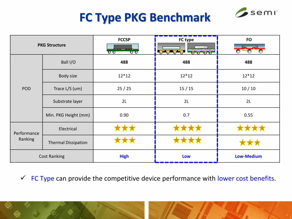
PKG Structure FCCSP FC type FO
POD
Ball I/O 488 488 488
Body size 12*12 12*12 12*12
Trace L/S (um) 25 / 25 15 / 15 10 / 10
Substrate layer 2L 2L 2L
Min. PKG Height (mm) 0.90 0.7 0.55
Performance Ranking
Electrical
Thermal Dissipation
Cost Ranking High Low Low-Medium
FC Type PKG Benchmark
FC Type can provide the competitive device performance with lower cost benefits.
Outline
• Introduction of Embedded Technology
• Package Features & KEY Drivers
• Challenges & its Solutions
• Future Developing Roadmap
• Conclusions
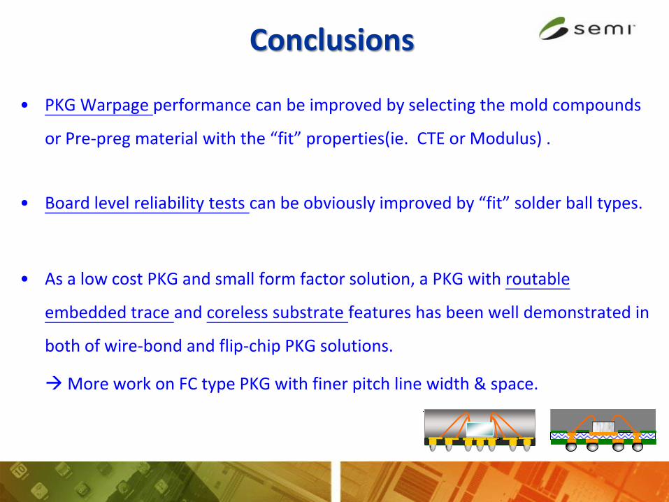
Conclusions
• PKG Warpage performance can be improved by selecting the mold compounds
or Pre-preg material with the “fit” properties(ie. CTE or Modulus) .
• Board level reliability tests can be obviously improved by “fit” solder ball types.
• As a low cost PKG and small form factor solution, a PKG with routable
embedded trace and coreless substrate features has been well demonstrated in
both of wire-bond and flip-chip PKG solutions.
More work on FC type PKG with finer pitch line width & space.

Contact Information:
藍章益
Solution Providing Innovative Leader


![Warpage Issues and Assembly Challenges Using …. Timoshenko et al. [12] ... structure is modified to bilayer structure. Coreless substrate is easily varied from smile to cry shape](https://img.pdfslide.net/doc/110x75/5ae2465b7f8b9a097a8cb8db/warpage-issues-and-assembly-challenges-using-timoshenko-et-al-12-structure.jpg)


![Magnetic quasi-static simulation [coreless liquid-cooled motor]](https://img.pdfslide.net/doc/110x75/56816864550346895ddeb859/magnetic-quasi-static-simulation-coreless-liquid-cooled-motor.jpg)