Embed Size (px)
Citation preview
A view on the Silicon Photonics trends and Market prospective
Jean Louis Malinge2nd Summer School on INtelligent signal processing for FrontIEr Research and Industry July 22nd 2014
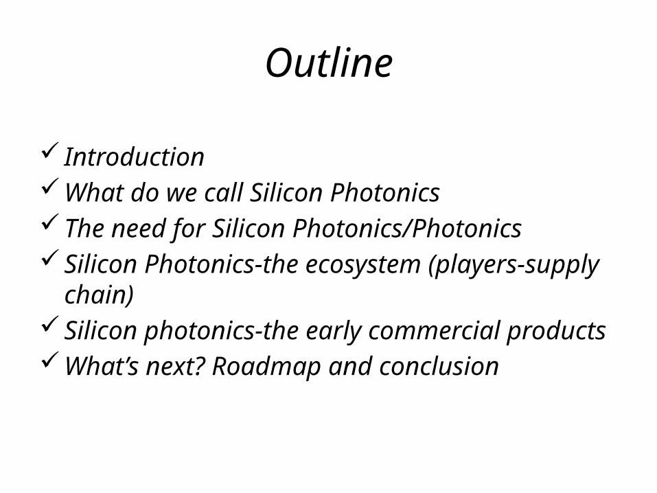
Outline
IntroductionWhat do we call Silicon PhotonicsThe need for Silicon Photonics/Photonics Silicon Photonics-the ecosystem (players-supply
chain) Silicon photonics-the early commercial productsWhat’s next? Roadmap and conclusion
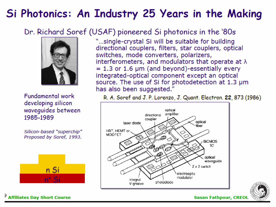
Introduction My objective is to give you a broad overview of the Silicon
Photonics trends and Market/application prospective Although the Silicon Photonics platform has been pioneered for
25 years this is still a technology in its infancy with a broad worldwide academic effort, numerous start-ups founded around the world and large corporations spending large R&D budget.
This presentation was built from my experience as CEO of Kotura in California which I recently sold to Mellanox technologies www.mellanox.com and a contribution done in the last few months to a market analysis published by Yole Development www.yole.fr – www.i-micronews.com
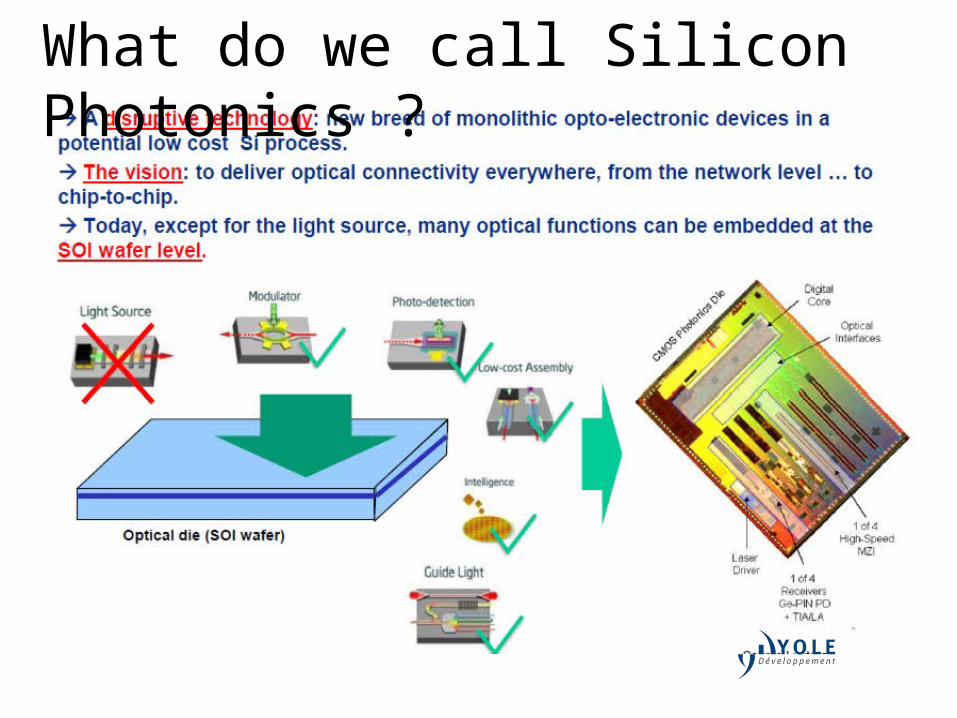
What do we call Silicon Photonics ?
Kotura Company Proprietary
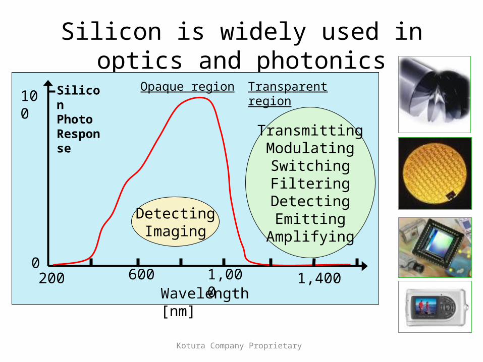
Silicon is widely used in optics and photonics
Silicon Photo Response
Wavelength [nm]
0
100
200 1,400600 1,000
DetectingImaging
TransmittingModulatingSwitchingFiltering
DetectingEmitting
Amplifying
Transparent regionOpaque region
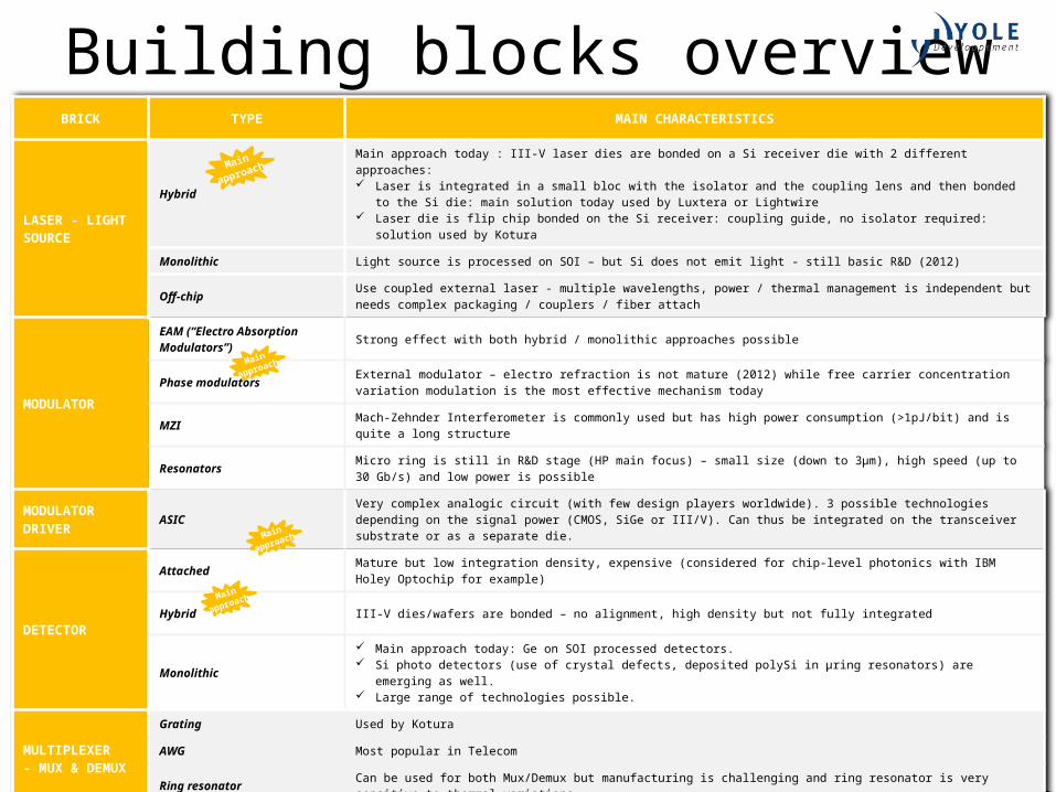
Building blocks overviewBRICK TYPE MAIN CHARACTERISTICS
LASER - LIGHT SOURCE
HybridMain approach today : III-V laser dies are bonded on a Si receiver die with 2 different approaches: Laser is integrated in a small bloc with the isolator and the coupling lens and then bonded to the Si die: main solution today used by
Luxtera or Lightwire Laser die is flip chip bonded on the Si receiver: coupling guide, no isolator required: solution used by Kotura
Monolithic Light source is processed on SOI – but Si does not emit light - still basic R&D (2012)
Off-chip Use coupled external laser - multiple wavelengths, power / thermal management is independent but needs complex packaging / couplers / fiber attach
MODULATOR
EAM (“Electro Absorption Modulators”) Strong effect with both hybrid / monolithic approaches possible
Phase modulators External modulator – electro refraction is not mature (2012) while free carrier concentration variation modulation is the most effective mechanism today
MZI Mach-Zehnder Interferometer is commonly used but has high power consumption (>1pJ/bit) and is quite a long structure
Resonators Micro ring is still in R&D stage (HP main focus) – small size (down to 3µm), high speed (up to 30 Gb/s) and low power is possible
MODULATOR DRIVER ASIC Very complex analogic circuit (with few design players worldwide). 3 possible technologies depending on the signal power (CMOS, SiGe or
III/V). Can thus be integrated on the transceiver substrate or as a separate die.
DETECTOR
Attached Mature but low integration density, expensive (considered for chip-level photonics with IBM Holey Optochip for example)
Hybrid III-V dies/wafers are bonded – no alignment, high density but not fully integrated
Monolithic Main approach today: Ge on SOI processed detectors. Si photo detectors (use of crystal defects, deposited polySi in µring resonators) are emerging as well. Large range of technologies possible.
MULTIPLEXER- MUX & DEMUX
Grating Used by Kotura
AWG Most popular in Telecom
Ring resonator Can be used for both Mux/Demux but manufacturing is challenging and ring resonator is very sensitive to thermal variations
COUPLERS Evanescent, grating, inverted taper etc … Allows fiber-to-chip or intra-chip coupling. Gratings on Si are today mostly used.
OTHERS Waveguides, splitters, Trans Impedance Amplifier (TIA)…
SOI is well suited for waveguide because of high difference in refractive index. Different technologies: Rib/ridge WG, Strip/Wire WG, photonic crystal WG, Slot WG Different waveguide dimensions/technologies:
3 µm x 3µm with Kotura. Bigger waveguide meaning higher signal power handled. Interesting approach for transceivers. Electronic and Optics functions are independent, need for bonding or via technology to connect both.
0.4 µm x 0.4 µm by Luxtera. Historically for better electronic & photonic integration and easier manufacturing
Main
approach
Main
approach
Main
approach
Main
approach
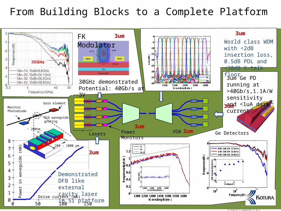
From Building Blocks to a Complete Platform
01
23
45
67
8
0 50 100 150Drive current (mA)
Pow
er in
wav
egui
de (m
W)
Monitor Photodiode
Gain element
Rib waveguidegrating
~ 200nm
200 - 1000 µm
108 109 1010-9
-6
-3
0
Frequncy(Hz)
Res
pons
e(dB
)
-0.0V: 3dB BW 17.5GHz-1.0V: 3dB BW 32.6GHz-3.0V: 3dB BW 36.8GHz
0 1 2 310
20
30
40
Voltage(V)
3dB
Ban
dwid
th(G
Hz)
1300 1350 1400 1450 1500 1550 16000
0.2
0.4
0.6
0.8
1
1.2
Wavelength(nm)
Res
pons
ivity
(A/W
)
TETMLimit
1300 1400 1500 1600-2
-1
0
1
2
Wavelength(nm)
PDR
(dB
)
1520 1540 1560 1580 1600-40
-35
-30
-25
-20
-15
-10
-5
0
Wavelength(nm)
Loss
(dB
)
TETM
Demonstrated DFB like external cavity laser in Si platform
Ge DetectorsVOALasers Power Monitors
3um Ge PD running at >40Gb/s,1.1A/W sensitivity and <1uA dark current
World class WDM with <2dB insertion loss, 0.5dB PDL and <30dB X-talk floor
3um
3um
3um
3um3um
FK Modulator3um
30GHz demonstratedPotential: 40Gb/s at 3V
7 strictly private and confidential
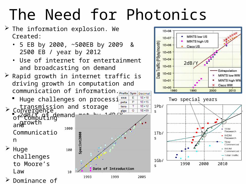
The Need for Photonics: Root Cause The information explosion. We Created:
• 5 EB by 2000, ~500EB by 2009 & 2500 EB / year by 2012
• Use of internet for entertainment and broadcasting on demand
Rapid growth in internet traffic is driving growth in computation and communication of information. Huge challenges on processing, transmission and
storage 2dB/Y of demand met by 1dB/Y growth
2dB/Y
1Gb/s
1Tb/s
1Pb/s
1990 20102000
Two special years
10
100
1000
Date of Introduction
Spec
Int2
000
1993 1999 2005
Convergence of Computing and Communication
Huge challenges to Moore’s Law
Dominance of power and energy!
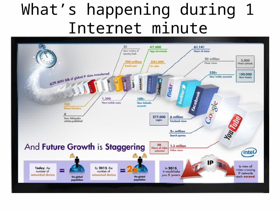
What’s happening during 1 Internet minute
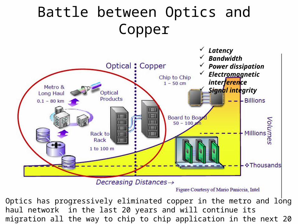
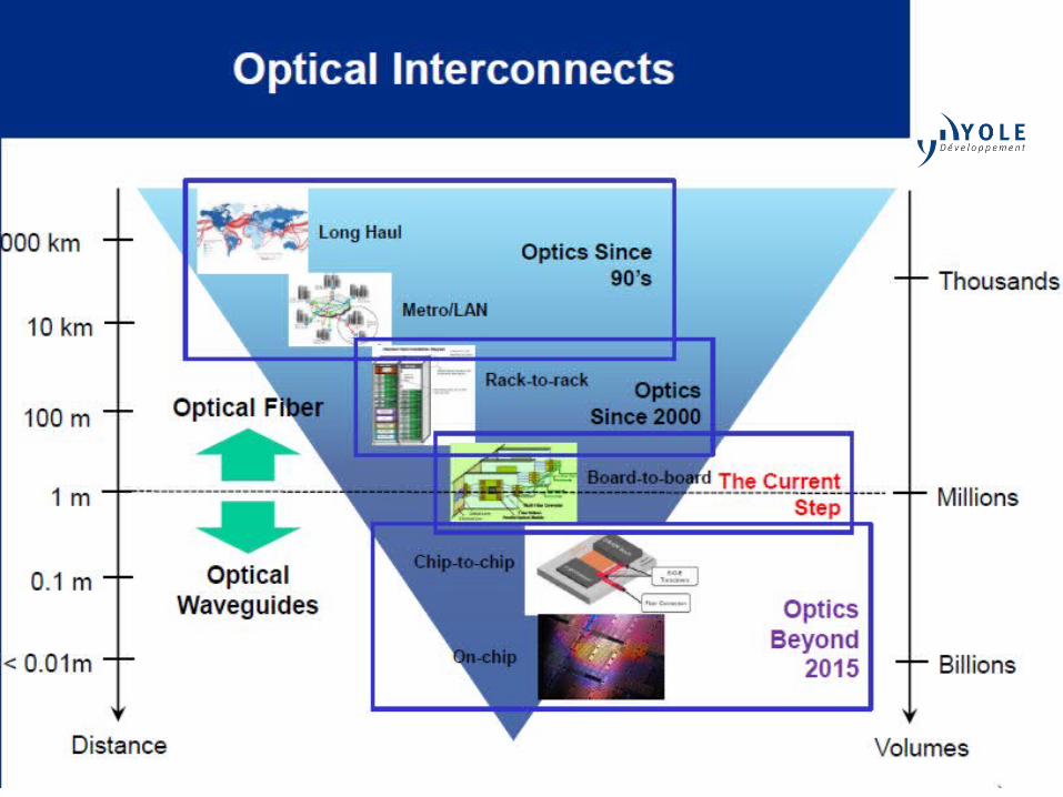
Battle between Optics and Copper
Optics has progressively eliminated copper in the metro and long haul network in the last 20 years and will continue its migration all the way to chip to chip application in the next 20 years
Latency Bandwidth Power dissipation Electromagnetic interference Signal integrity
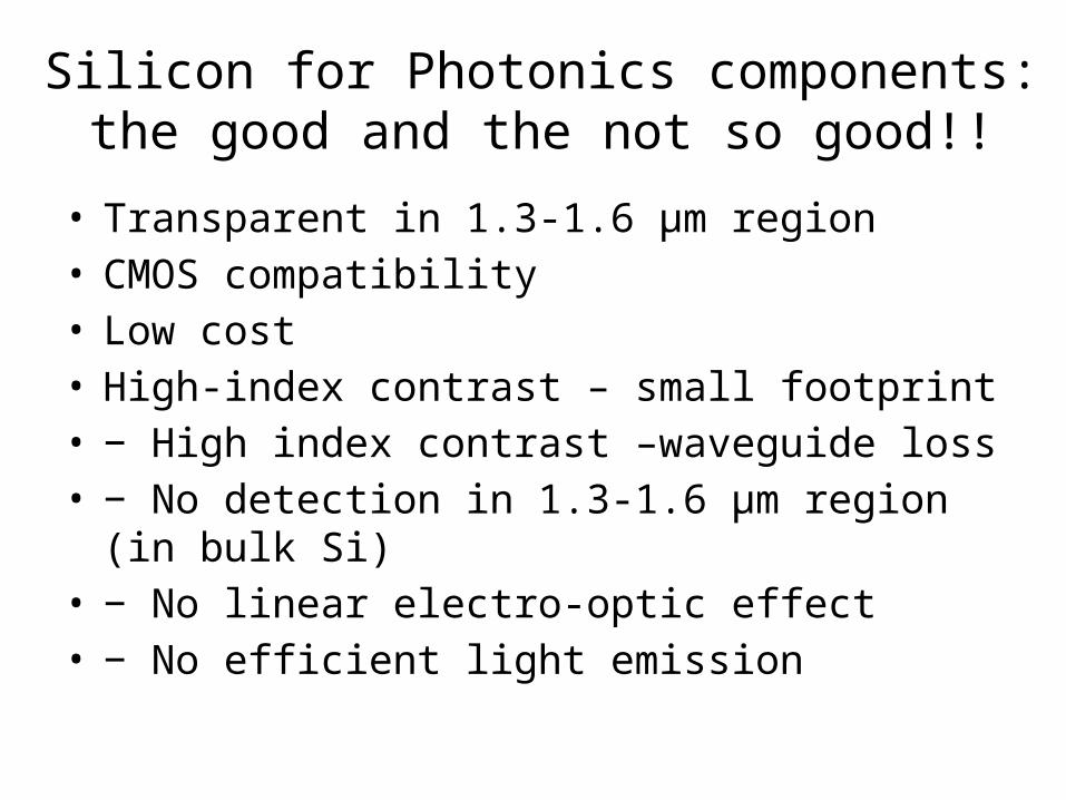
Silicon for Photonics components: the good and the not so good!!
• Transparent in 1.3-1.6 µm region• CMOS compatibility • Low cost• High-index contrast – small footprint• − High index contrast –waveguide loss• − No detection in 1.3-1.6 µm region (in bulk Si)• − No linear electro-optic effect• − No efficient light emission
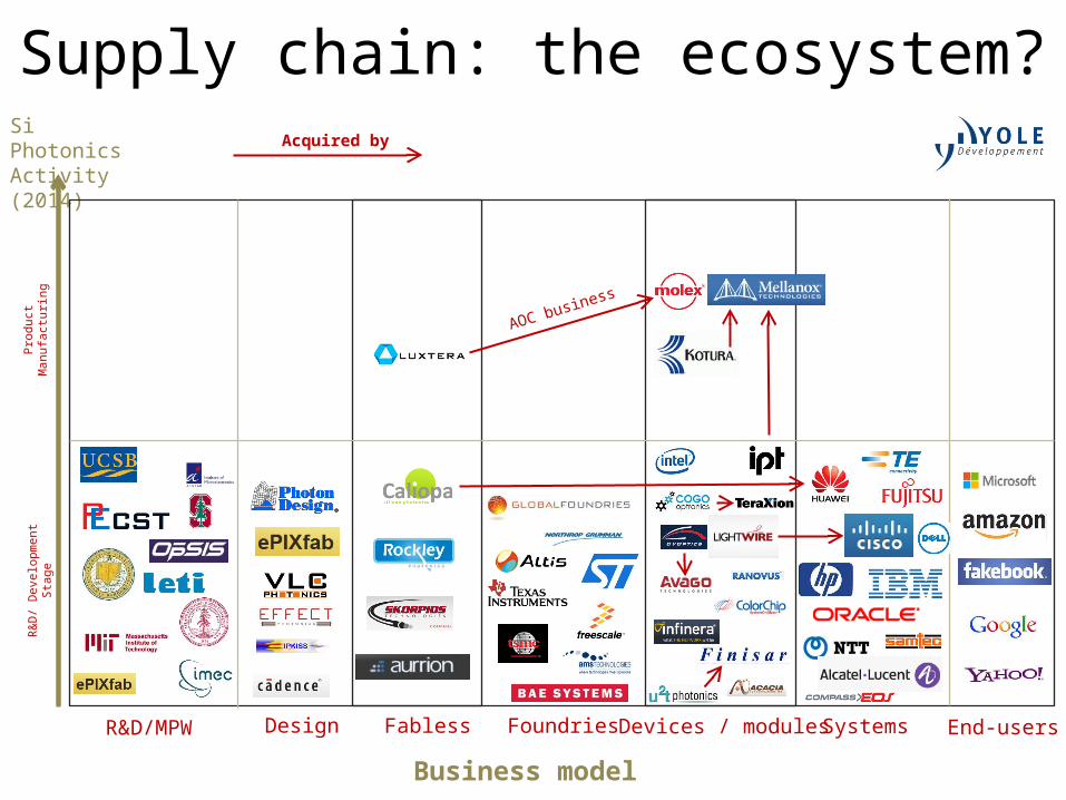
Supply chain: the ecosystem?Si Photonics Activity (2014)
Business model
Prod
uct M
anuf
actu
ring
R&D/
Dev
elop
men
t St
age
R&D/MPW Devices / modulesFoundriesFabless Systems End-usersDesign
Acquired by
AOC business
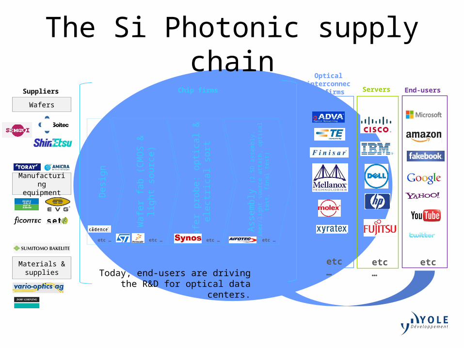
The Si Photonic supply chainSuppliers Chip firms
Optical interconnects
firms Servers End-users
Wafers
Manufacturing equipment
Materials & supplies
Desig
n
Waf
er fa
b (C
MO
S &
ligh
t sou
rce)
Waf
er p
robe
: opti
cal &
ele
ctric
al
sort
Asse
mbl
y (2
.5D
asse
mbl
y, fi
ber/
light
sour
ce
attac
h, o
ptica
l tes
t, fin
al te
st)
v
etc … etc … etc …Today, end-users are driving the R&D for
optical data centers.
etc … etc … etc … etc …
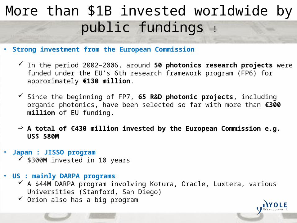
More than $1B invested worldwide by public fundings !
• Strong investment from the European Commission
In the period 2002–2006, around 50 photonics research projects were funded under the EU’s 6th research framework program (FP6) for approximately €130 million.
Since the beginning of FP7, 65 R&D photonic projects, including organic photonics, have been selected so far with more than €300 million of EU funding.
Þ A total of €430 million invested by the European Commission e.g. US$ 580M
• Japan : JISSO program $300M invested in 10 years
• US : mainly DARPA programs A $44M DARPA program involving Kotura, Oracle, Luxtera, various Universities (Stanford, San Diego) Orion also has a big program
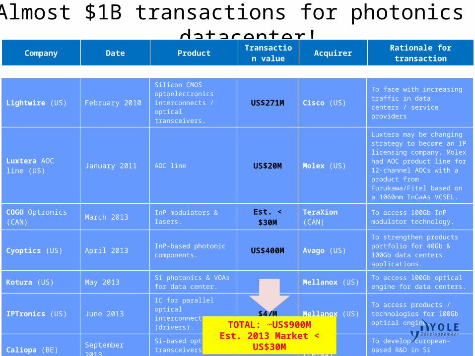
Almost $1B transactions for photonics in datacenter!
Lightwire (US) February 2010Silicon CMOS optoelectronics interconnects / optical transceivers.
US$271M Cisco (US) To face with increasing traffic in data centers / service providers
Luxtera AOC line (US) January 2011 AOC line US$20M Molex (US)
Luxtera may be changing strategy to become an IP licensing company. Molex had AOC product line for 12-channel AOCs with a product from Furukawa/Fitel based on a 1060nm InGaAs VCSEL.
COGO Optronics (CAN) March 2013 InP modulators & lasers. Est. < $30M TeraXion (CAN) To access 100Gb InP modulator technology.
Cyoptics (US) April 2013 InP-based photonic components. US$400M Avago (US)
To strengthen products portfolio for 40Gb & 100Gb data centers applications.
Kotura (US) May 2013 Si photonics & VOAs for data center. $82M Mellanox (US) To access 100Gb optical engine for
data centers.
IPTronics (US) June 2013 IC for parallel optical interconnects (drivers). $47M Mellanox (US) To access products / technologies
for 100Gb optical engine.
Caliopa (BE) September 2013 Si-based optical transceivers for datacoms. $20M Huawei (CHINA) To develop European-based R&D in
Si photonics.
Company Date Product Transaction value Acquirer Rationale for transaction
TOTAL: ~US$900MEst. 2013 Market < US$30M
© 2014• 18
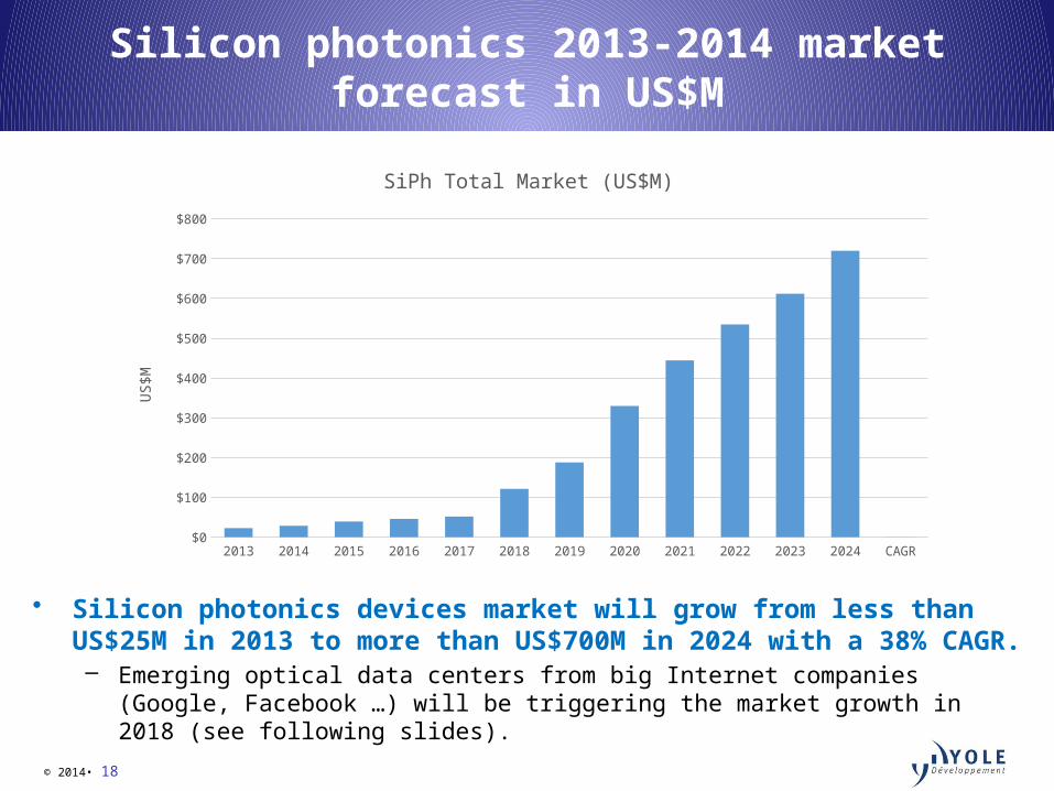
Silicon photonics 2013-2014 market forecast in US$M
• Silicon photonics devices market will grow from less than US$25M in 2013 to more than US$700M in 2024 with a 38% CAGR.– Emerging optical data centers from big Internet companies (Google, Facebook …) will
be triggering the market growth in 2018 (see following slides).
2013 2014 2015 2016 2017 2018 2019 2020 2021 2022 2023 2024 CAGR$0
$100
$200
$300
$400
$500
$600
$700
$800
SiPh Total Market (US$M)
US$M
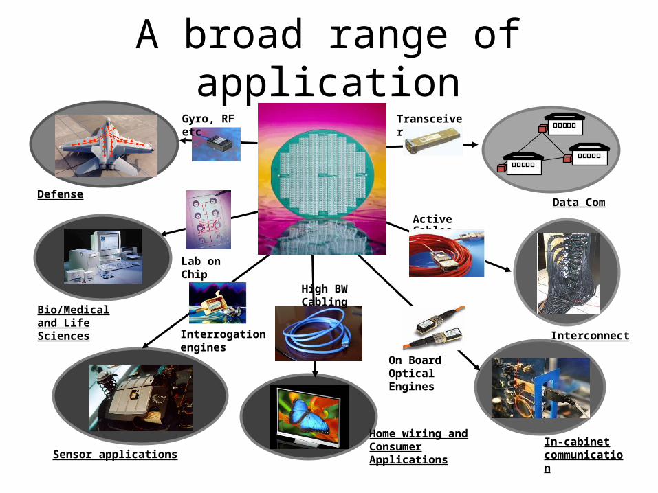
A broad range of application
Data Com
Interconnect
Transceivers
Active Cables
Sensor applicationsIn-cabinet communication
Home wiring and Consumer Applications
High BW Cabling
Interrogation engines
On Board Optical Engines
Lab on Chip
Bio/Medical and Life Sciences
Gyro, RF etc
Defense
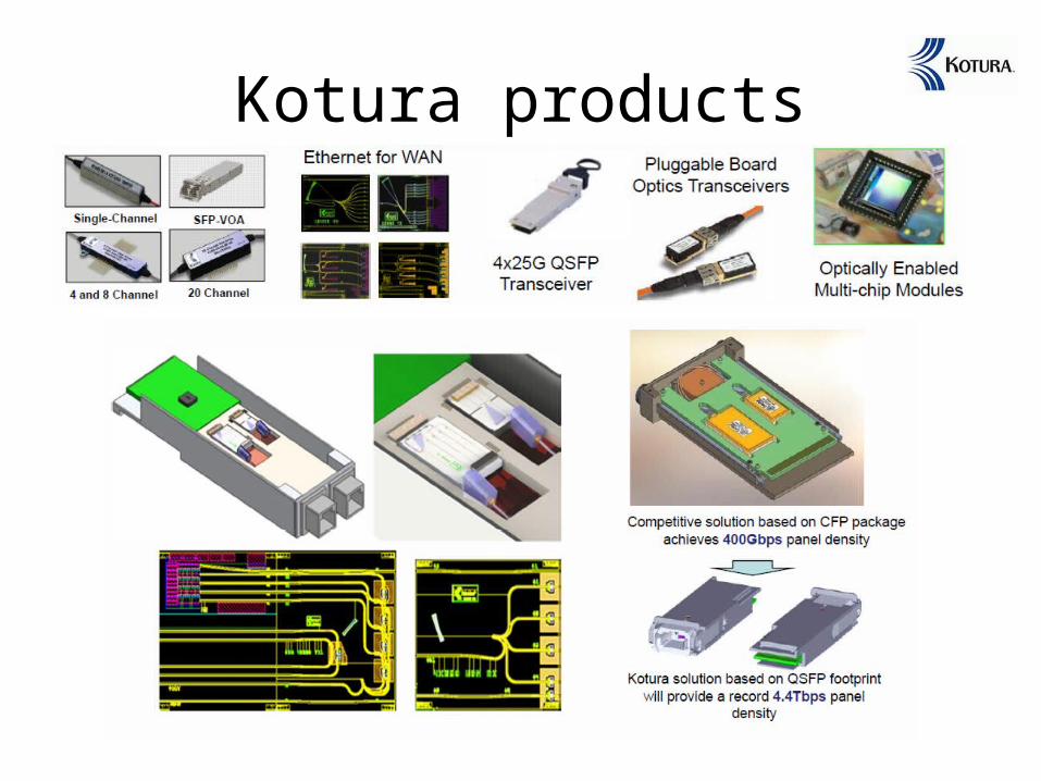
Kotura products
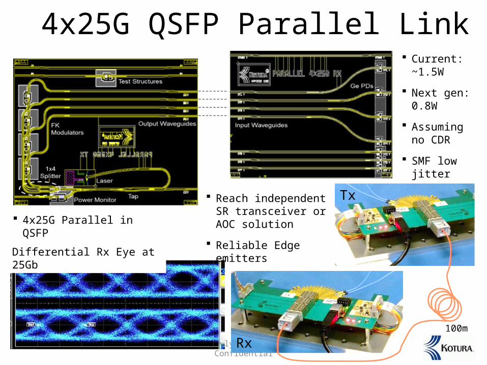
4x25G QSFP Parallel Link
Strictly Private and Confidential
Differential Rx Eye at 25Gb
Rx
Tx
100m
Reach independent SR transceiver or AOC solution
Reliable Edge emitters
Current: ~1.5W
Next gen: 0.8W
Assuming no CDR
SMF low jitter
4x25G Parallel in QSFP
22
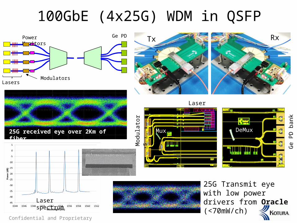
100GbE (4x25G) WDM in QSFP
Confidential and Proprietary
RxTx
25G Transmit eye with low power drivers from Oracle (<70mW/ch)
25G received eye over 2Km of fiber
Ge PD
Lasers
Power Monitors
Modulators
Laser bank
Mod
ulat
ors
Mux DeMux
Ge P
D ba
nk
Laser spectrum
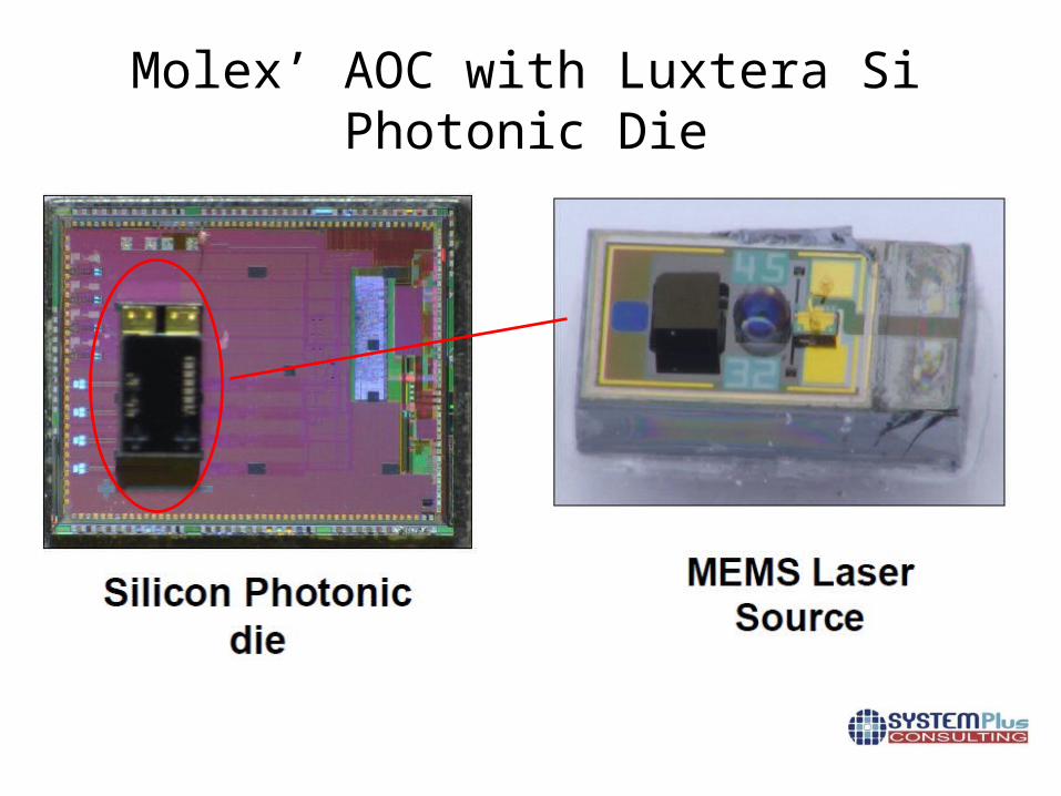
Molex’ AOC with Luxtera Si Photonic Die
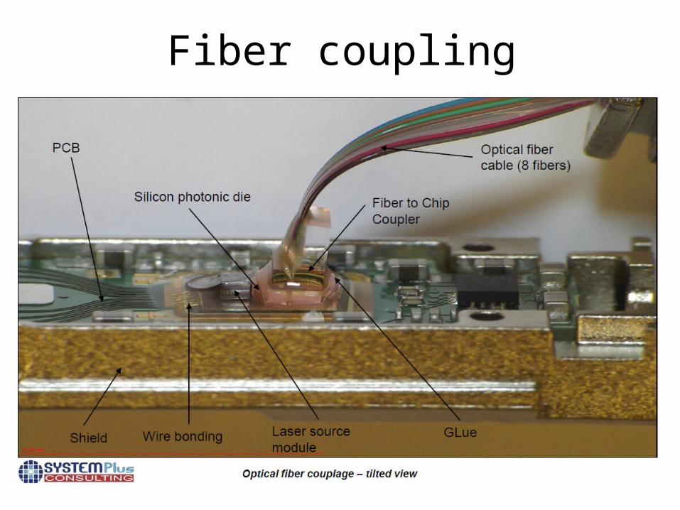
Fiber coupling
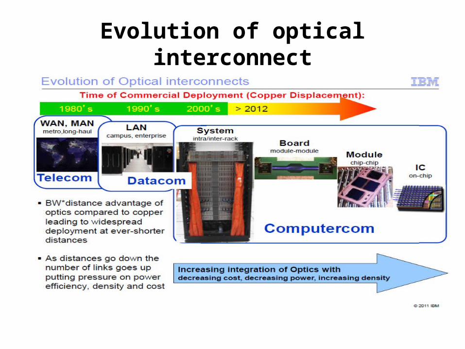
Evolution of optical interconnect
Summary Clear need/technology gap created by the explosive growth of
Data/image communication
Photonics /Silicon Photonics will be the platform of choice for interconnect resolving the major current technological issues: latency, bandwidth, power dissipation and signal integrity.
A world wide ecosystem has developed over the last 10 years to generate the supply chain
This is still a market in its infancy with challenges to be resolved: laser integration, low cost integration/ packaging/ standardization….