Embed Size (px)
Citation preview
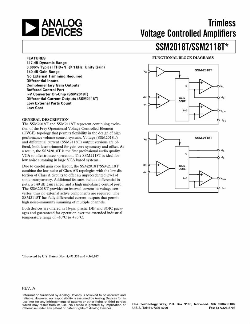
FUNCTIONAL BLOCK DIAGRAMS
GENERAL DESCRIPTIONThe SSM2018T and SSM2118T represent continuing evolu-tion of the Frey Operational Voltage Controlled Element(OVCE) topology that permits flexibility in the design of highperformance volume control systems. Voltage (SSM2018T)and differential current (SSM2118T) output versions are of-fered, both laser-trimmed for gain core symmetry and offset. Asa result, the SSM2018T is the first professional audio qualityVCA to offer trimless operation. The SSM2118T is ideal forlow noise summing in large VCA based systems.
Due to careful gain core layout, the SSM2018T/SSM2118Tcombine the low noise of Class AB topologies with the low dis-tortion of Class A circuits to offer an unprecedented level ofsonic transparency. Additional features include differential in-puts, a 140 dB gain range, and a high impedance control port.The SSM2018T provides an internal current-to-voltage con-verter; thus no external active components are required. TheSSM2118T has fully differential current outputs that permithigh noise-immunity summing of multiple channels.
Both devices are offered in 16-pin plastic DIP and SOIC pack-ages and guaranteed for operation over the extended industrialtemperature range of –40°C to +85°C.
*Protected by U.S. Patent Nos. 4,471,320 and 4,560,947.
FEATURES
117 dB Dynamic Range
0.006% Typical THD+N (@ 1 kHz, Unity Gain)
140 dB Gain Range
No External Trimming Required
Differential Inputs
Complementary Gain Outputs
Buffered Control Port
I–V Converter On-Chip (SSM2018T)
Differential Current Outputs (SSM2118T)
Low External Parts Count
Low Cost
TrimlessVoltage Controlled Amplifiers
SSM2018T/SSM2118T*
Information furnished by Analog Devices is believed to be accurate andreliable. However, no responsibility is assumed by Analog Devices for itsuse, nor for any infringements of patents or other rights of third partieswhich may result from its use. No license is granted by implication orotherwise under any patent or patent rights of Analog Devices.
One Technology Way, P.O. Box 9106, Norwood. MA 02062-9106,
U.S.A. Tel: 617/329-4700 Fax: 617/326-8703
REV. A
a
VC
–IN
+IN
VG
V1–G
–IG
–I1–G
GAINCORE
G
1–G
SSM-2018T
VC
–IN
+IN
+IG
V1–G
–IG
–I1–G
GAINCORE
G
1–G
SSM-2118T
REV. A–2–
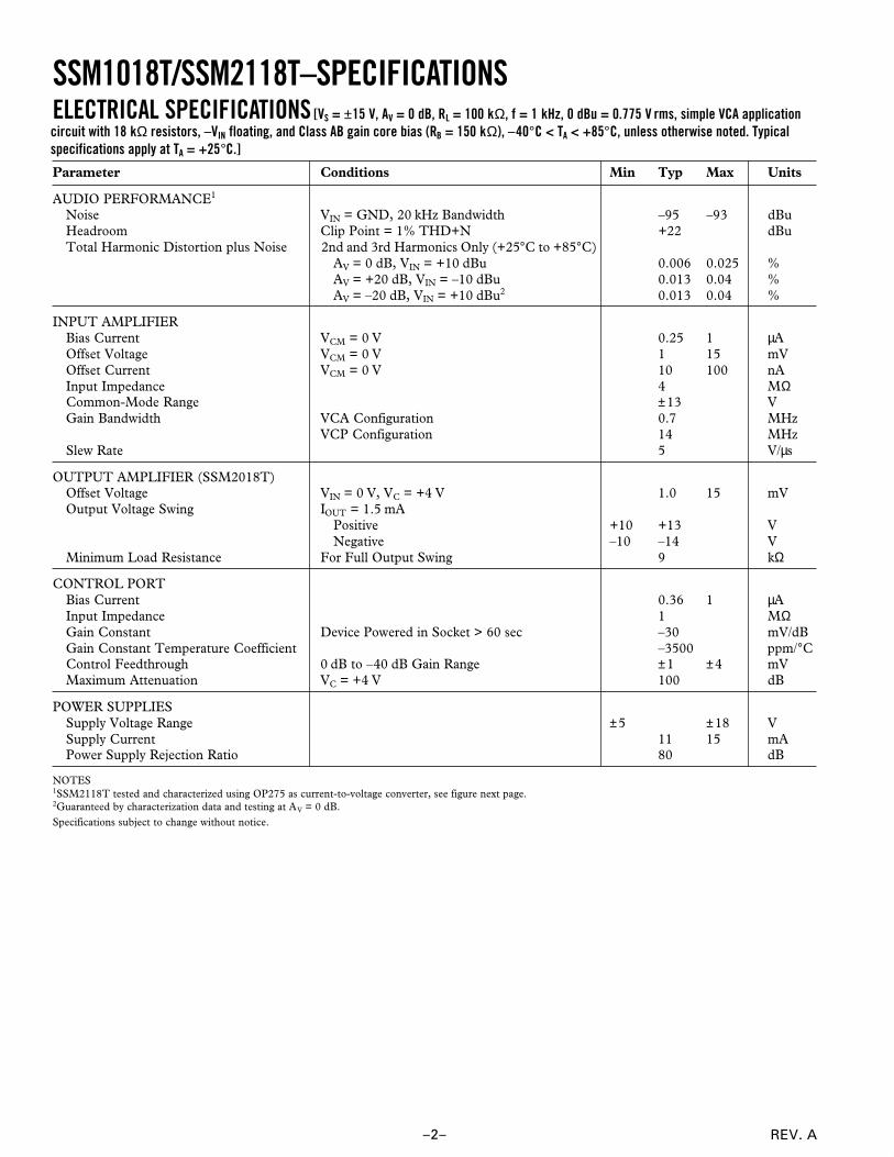
SSM1018T/SSM2118T–SPECIFICATIONSELECTRICAL SPECIFICATIONS
Parameter Conditions Min Typ Max Units
AUDIO PERFORMANCE1
Noise VIN = GND, 20 kHz Bandwidth –95 –93 dBuHeadroom Clip Point = 1% THD+N +22 dBuTotal Harmonic Distortion plus Noise 2nd and 3rd Harmonics Only (+25°C to +85°C)
AV = 0 dB, VIN = +10 dBu 0.006 0.025 %AV = +20 dB, VIN = –10 dBu 0.013 0.04 %AV = –20 dB, VIN = +10 dBu2 0.013 0.04 %
INPUT AMPLIFIERBias Current VCM = 0 V 0.25 1 µAOffset Voltage VCM = 0 V 1 15 mVOffset Current VCM = 0 V 10 100 nAInput Impedance 4 MΩCommon-Mode Range ±13 VGain Bandwidth VCA Configuration 0.7 MHz
VCP Configuration 14 MHzSlew Rate 5 V/µs
OUTPUT AMPLIFIER (SSM2018T)Offset Voltage VIN = 0 V, VC = +4 V 1.0 15 mVOutput Voltage Swing IOUT = 1.5 mA
Positive +10 +13 VNegative –10 –14 V
Minimum Load Resistance For Full Output Swing 9 kΩ
CONTROL PORTBias Current 0.36 1 µAInput Impedance 1 MΩGain Constant Device Powered in Socket > 60 sec –30 mV/dBGain Constant Temperature Coefficient –3500 ppm/°CControl Feedthrough 0 dB to –40 dB Gain Range ±1 ±4 mVMaximum Attenuation VC = +4 V 100 dB
POWER SUPPLIESSupply Voltage Range ±5 ±18 VSupply Current 11 15 mAPower Supply Rejection Ratio 80 dB
NOTES1SSM2118T tested and characterized using OP275 as current-to-voltage converter, see figure next page.2Guaranteed by characterization data and testing at AV = 0 dB.
Specifications subject to change without notice.
[VS = ±15 V, AV = 0 dB, RL = 100 kΩ, f = 1 kHz, 0 dBu = 0.775 V rms, simple VCA applicationcircuit with 18 kΩ resistors, –VIN floating, and Class AB gain core bias (RB = 150 kΩ), –40°C < TA < +85°C, unless otherwise noted. Typicalspecifications apply at TA = +25°C.]
REV. A –3–
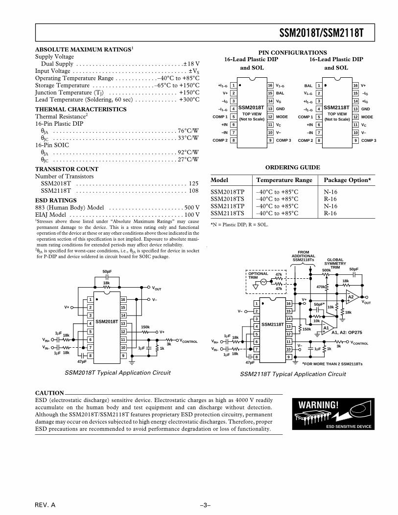
SSM2018T/SSM2118TABSOLUTE MAXIMUM RATINGS1
Supply VoltageDual Supply . . . . . . . . . . . . . . . . . . . . . . . . . . . . . . . . .±18 V
Input Voltage . . . . . . . . . . . . . . . . . . . . . . . . . . . . . . . . . . . ±VS
Operating Temperature Range . . . . . . . . . . . . . –40°C to +85°CStorage Temperature . . . . . . . . . . . . . . . . . . . –65°C to +150°CJunction Temperature (TJ) . . . . . . . . . . . . . . . . . . . . . +150°CLead Temperature (Soldering, 60 sec) . . . . . . . . . . . . . +300°CTHERMAL CHARACTERISTICSThermal Resistance2
16-Pin Plastic DIPθJA . . . . . . . . . . . . . . . . . . . . . . . . . . . . . . . . . . . . . . 76°C/WθJC . . . . . . . . . . . . . . . . . . . . . . . . . . . . . . . . . . . . . . 33°C/W
16-Pin SOICθJA . . . . . . . . . . . . . . . . . . . . . . . . . . . . . . . . . . . . . . 92°C/WθJC . . . . . . . . . . . . . . . . . . . . . . . . . . . . . . . . . . . . . . 27°C/W
TRANSISTOR COUNTNumber of Transistors
SSM2018T . . . . . . . . . . . . . . . . . . . . . . . . . . . . . . . . . . 125SSM2118T . . . . . . . . . . . . . . . . . . . . . . . . . . . . . . . . . . 108
ESD RATINGS883 (Human Body) Model . . . . . . . . . . . . . . . . . . . . . . . 500 VEIAJ Model . . . . . . . . . . . . . . . . . . . . . . . . . . . . . . . . . . . 100 V1Stresses above those listed under “Absolute Maximum Ratings” may causepermanent damage to the device. This is a stress rating only and functionaloperation of the device at these or any other conditions above those indicated in theoperation section of this specification is not implied. Exposure to absolute maxi-mum rating conditions for extended periods may affect device reliability.
2θJA is specified for worst-case conditions, i.e., θJA is specified for device in socketfor P-DIP and device soldered in circuit board for SOIC package.
ORDERING GUIDE
Model Temperature Range Package Option*
SSM2018TP –40°C to +85°C N-16SSM2018TS –40°C to +85°C R-16SSM2118TP –40°C to +85°C N-16SSM2118TS –40°C to +85°C R-16
*N = Plastic DIP; R = SOL.
PIN CONFIGURATIONS16-Lead Plastic DIP
and SOL16-Lead Plastic DIP
and SOL
+I1–G
V+ BAL
COMP 1
+IN
–IN
MODE
VC
V–
–I1–G
–IG VG
GND
COMP 2 COMP 3
1
2
16
15
5
6
7
12
11
10
3
4
14
13
8 9
TOP VIEW(Not to Scale)
SSM2018T
V1–G
+I1–G
V+BAL
COMP 1
+IN
–IN
MODE
VC
V–
–I1–G GND
COMP 2 COMP 3
1
2
16
15
5
6
7
12
11
10
3
4
14
13
8 9
TOP VIEW(Not to Scale)
SSM2118T
V1–G –IG
+IG
SSM2018T Typical Application Circuit SSM2118T Typical Application Circuit
1µF 18kVIN+
V–
150k A1
10k
10k
18k
18k
500k 50pF
VOUT
GLOBALSYMMETRY
TRIM
FROMADDITIONALSSM2118Ts
V–
1µF 18kVIN–
47pF
1µF3k
VCONTROL
V+50pF*
470k
OPTIONAL TRIM
47k
47k
A1, A2: OP275
1
2
5
6
7
3
4
8
16
15
12
11
10
14
13
9
SSM2118T
A2
1k
*FOR MORE THAN 2 SSM2118Ts
WARNING!
ESD SENSITIVE DEVICE
CAUTIONESD (electrostatic discharge) sensitive device. Electrostatic charges as high as 4000 V readilyaccumulate on the human body and test equipment and can discharge without detection.Although the SSM2018T/SSM2118T features proprietary ESD protection circuitry, permanentdamage may occur on devices subjected to high energy electrostatic discharges. Therefore, properESD precautions are recommended to avoid performance degradation or loss of functionality.
V+1µF
150k
18k
V+
18kVIN+
1µF 18kVIN–
47pF
1µF
50pF
1k
VCONTROL3k
VOUT
V–1
2
16
15
5
6
7
12
11
10
3
4
14
13
8 9
SSM2018T
–4–
SSM2018T/SSM2118T–Typical Characteristics
REV. A
0.1
0.010
0.001
TH
D +
N –
%
20 100 1k 10k 20kFREQUENCY – Hz
AV = +20dB
AV = –20dB
AV = 0dB
TA = +25°C VS = ±15V RF = 18kΩ
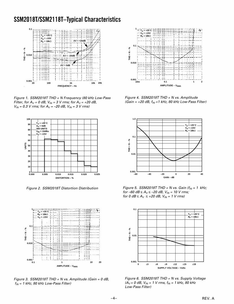
Figure 1. SSM2018T THD + N Frequency (80 kHz Low-Pass
Filter, for AV = 0 dB, VIN = 3 V rms; for AV = +20 dB,
VIN = 0.3 V rms; for AV = –20 dB, VIN = 3 V rms)
100
00.025
30
10
20
0.000
60
40
50
70
80
90
0.0200.0150.0100.005
DISTORTION – %
UN
ITS
TA = +25°CAV = 0dB300 UNITSVIN = 10dBuVS = ±15V
Figure 2. SSM2018T Distortion Distribution
1
0.1
0.010
0.001
TH
D +
N –
%
0.1 1 10 20
AMPLITUDE – VRMS
TA = +25°CRF = 18kΩVS = ±15V
Figure 3. SSM2018T THD + N vs. Amplitude (Gain = 0 dB,
fIN = 1 kHz, 80 kHz Low-Pass Filter)
1
0.1
0.010
0.001
TH
D +
N –
%
10m 0.1 1 2
AMPLITUDE – VRMS
TA = +25°CVS = ±15VRF = 18kΩ
Figure 4. SSM2018T THD + N vs. Amplitude
(Gain = +20 dB, fIN =1 kHz, 80 kHz Low-Pass Filter)
1.0
0.01
0.001–60 –40 20–20
0.1
0 40
TA = +25°C VS = ±15V RF = 18kΩ
GAIN – dB
TH
D +
N –
%
Figure 5. SSM2018T THD + N vs. Gain (fIN = 1 kHz;
for –60 dB ≤ AV ≤ –20 dB, VIN = 10 V rms;
for 0 dB ≤ AV ≤ +20 dB, VIN = 1 V rms)
TH
D +
N –
%
0.1
0.0010 ±12
0.01
TA = +25°CRF = 18kΩ
±3 ±6 ±9 ±15 ±18
SUPPLY VOLTAGE – Volts
Figure 6. SSM2018T THD + N vs. Supply Voltage
(AV = 0 dB, VIN = 1 V rms, fIN = 1 kHz, 80 kHz
Low-Pass Filter)
REV. A –5–
SSM2018T/SSM2118T
LOAD RESISTANCE – Ω
MA
XIM
UM
OU
TP
UT
SW
ING
– V
PE
AK
±15
±12
0100 1k 100k10k
±9
±6
±3
RF = 18kΩTA = +25°CVS = ±15V
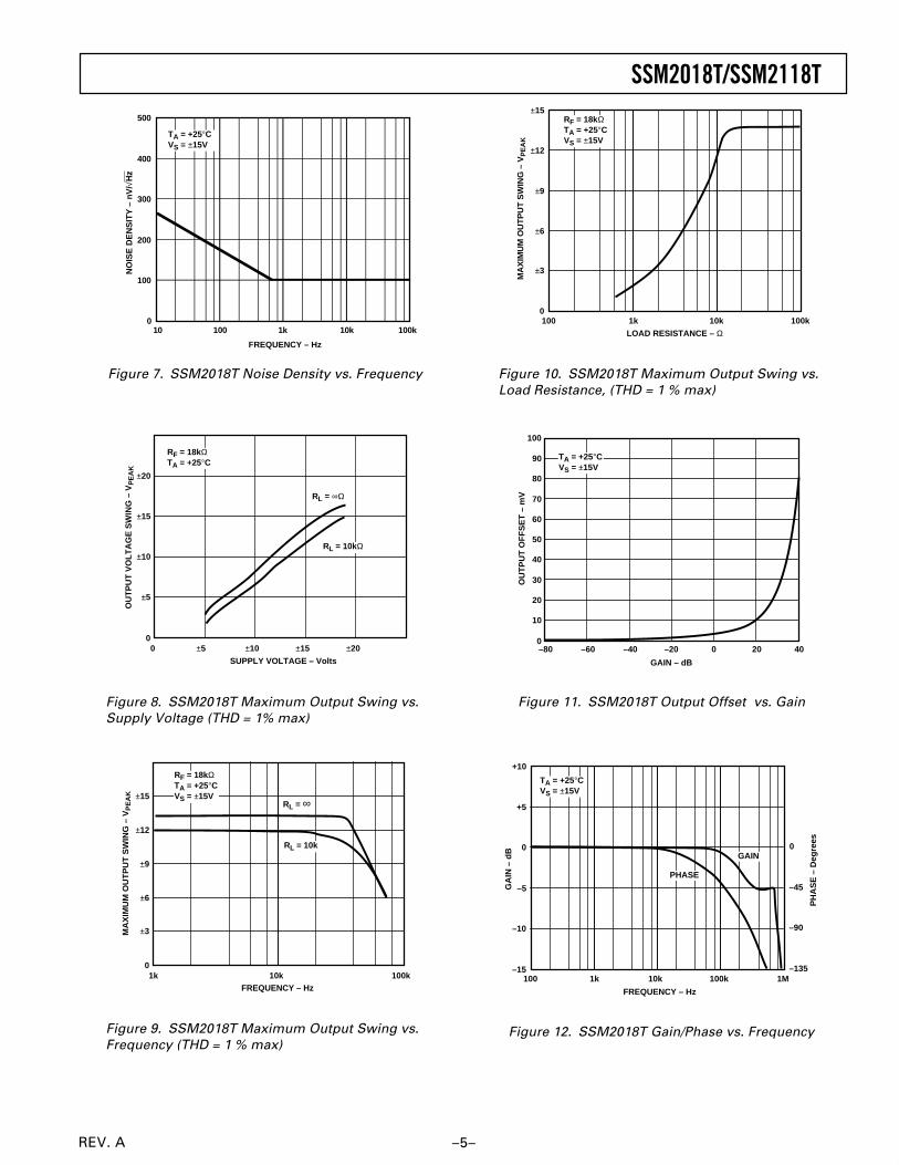
Figure 10. SSM2018T Maximum Output Swing vs.
Load Resistance, (THD = 1 % max)
100
040
30
10
–60
20
–80
60
40
50
70
80
90
200–20–40
TA = +25°CVS = ±15V
GAIN – dB
OU
TP
UT
OF
FS
ET
– m
V
Figure 11. SSM2018T Output Offset vs. Gain
+10
0
–151k 1M100k10k100
–5
–10
+5
FREQUENCY – Hz
TA = +25°CVS = ±15V
GA
IN –
dB 0
–135
–45
–90
PH
AS
E –
Deg
rees
GAIN
PHASE
Figure 12. SSM2018T Gain/Phase vs. Frequency
Figure 7. SSM2018T Noise Density vs. Frequency
0
±15
±5
±5
±10
0
±20
±20±15±10
SUPPLY VOLTAGE – Volts
OU
TP
UT
VO
LT
AG
E S
WIN
G –
VP
EA
K
RL = ∞Ω
RL = 10kΩ
RF = 18kΩTA = +25°C
Figure 8. SSM2018T Maximum Output Swing vs.
Supply Voltage (THD = 1% max)
FREQUENCY – Hz
MA
XIM
UM
OU
TP
UT
SW
ING
– V
PE
AK
RL = ∞
RL = 10k
RF = 18kΩTA = +25°CVS = ±15V
±9
01k 10k 100k
±3
±6
±12
±15
Figure 9. SSM2018T Maximum Output Swing vs.
Frequency (THD = 1 % max)
500
300
0100 100k10k1k10
200
100
400
FREQUENCY – Hz
NO
ISE
DE
NS
ITY
– n
V/√
Hz
TA = +25°CVS = ±15V
REV. A–6–
SSM2018T/SSM2118T–Typical Characteristics60
40
–80100 1k 10M1M100k10k
20
0
–20
–40
–60
FREQUENCY – Hz
TA = +25°CVS = ±15V
GA
IN –
dB
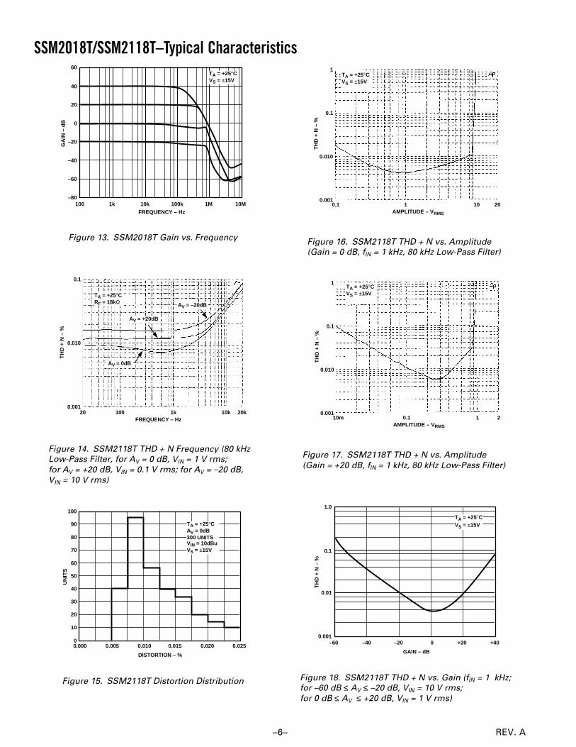
Figure 13. SSM2018T Gain vs. Frequency
TH
D +
N –
%
0.1
0.010
0.00120 100 1k 10k 20k
FREQUENCY – Hz
TA = +25°CRF = 18kΩ
AV = 0dB
AV = +20dB
AV = –20dB
Figure 14. SSM2118T THD + N Frequency (80 kHz
Low-Pass Filter, for AV = 0 dB, VIN = 1 V rms;
for AV = +20 dB, VIN = 0.1 V rms; for AV = –20 dB,
VIN = 10 V rms)
100
00.025
30
10
20
0.000
60
40
50
70
80
90
0.0200.0150.0100.005
DISTORTION – %
UN
ITS
TA = +25°CAV = 0dB300 UNITSVIN = 10dBuVS = ±15V
Figure 15. SSM2118T Distortion Distribution
AMPLITUDE – VRMS
TA = +25°CVS = ±15V
0.1 1 10 20
1
0.1
0.010
0.001
TH
D +
N –
%
Figure 16. SSM2118T THD + N vs. Amplitude
(Gain = 0 dB, fIN = 1 kHz, 80 kHz Low-Pass Filter)
AMPLITUDE – VRMS
TA = +25°CVS = ±15V
10m 0.1 1 2
1
0.1
0.010
0.001
TH
D +
N –
%
Figure 17. SSM2118T THD + N vs. Amplitude
(Gain = +20 dB, fIN = 1 kHz, 80 kHz Low-Pass Filter)
1.0
0.001–60 –40 –20 0 +20 +40
0.1
0.01
GAIN – dB
TH
D +
N –
%
TA = +25°CVS = ±15V
Figure 18. SSM2118T THD + N vs. Gain (fIN = 1 kHz;
for –60 dB ≤ AV ≤ –20 dB, VIN = 10 V rms;
for 0 dB ≤ AV ≤ +20 dB, VIN = 1 V rms)
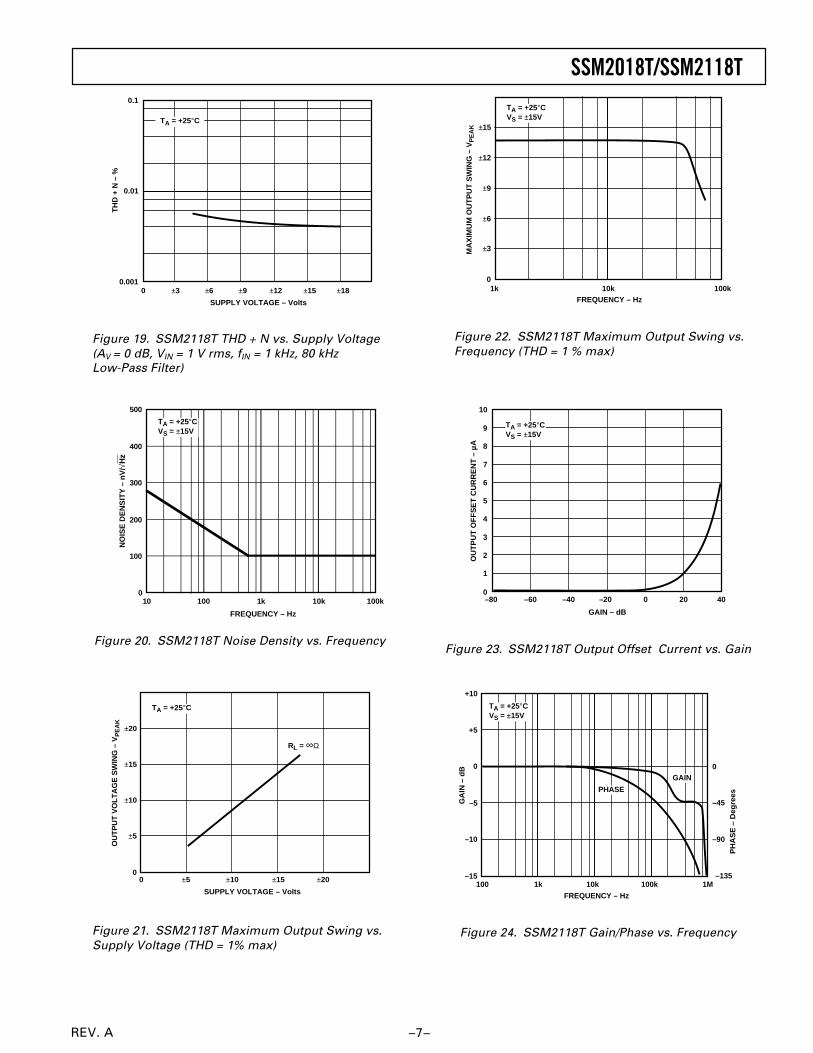
REV. A –7–
SSM2018T/SSM2118T
SUPPLY VOLTAGE – Volts
TH
D +
N –
%TA = +25°C
0.1
0.01
0.0010 ±3 ±6 ±9 ±12 ±15 ±18
Figure 19. SSM2118T THD + N vs. Supply Voltage
(AV = 0 dB, VIN = 1 V rms, fIN = 1 kHz, 80 kHz
Low-Pass Filter)
Figure 20. SSM2118T Noise Density vs. Frequency
0
±15
±5
±10
0 ±5 ±10 ±15 ±20
±20
SUPPLY VOLTAGE – Volts
OU
TP
UT
VO
LT
AG
E S
WIN
G –
VP
EA
K
RL = ∞Ω
±20
TA = +25°C
Figure 21. SSM2118T Maximum Output Swing vs.
Supply Voltage (THD = 1% max)
±9
01k 10k 100k
±3
±6
±12
±15
FREQUENCY – Hz
MA
XIM
UM
OU
TP
UT
SW
ING
– V
PE
AK
TA = +25°CVS = ±15V
Figure 22. SSM2118T Maximum Output Swing vs.
Frequency (THD = 1 % max)
10
040
3
1
–60
2
–80
6
4
5
7
8
9
200–20–40
GAIN – dB
OU
TP
UT
OF
FS
ET
CU
RR
EN
T –
µA
TA = +25°CVS = ±15V
Figure 23. SSM2118T Output Offset Current vs. Gain
+10
0
–151k 1M100k10k100
–5
–10
+5
FREQUENCY – Hz
GA
IN –
dB 0
–135
–45
–90
PH
AS
E –
Deg
rees
TA = +25°CVS = ±15V
PHASE
GAIN
Figure 24. SSM2118T Gain/Phase vs. Frequency
500
300
010 100 1k 10k 100k
200
100
400
TA = +25°CVS = ±15V
FREQUENCY – Hz
NO
ISE
DE
NS
ITY
– n
V/√
Hz
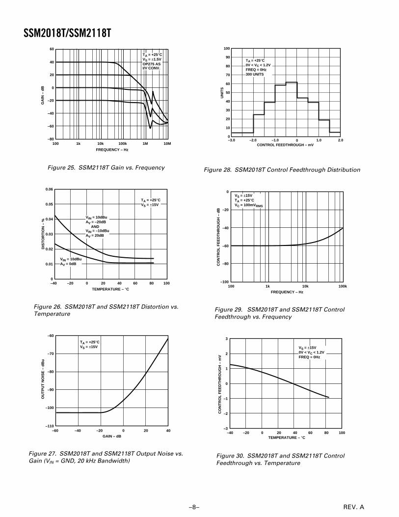
REV. A–8–
SSM2018T/SSM2118T60
40
–80100 1k 10M1M100k10k
20
0
–20
–40
–60
FREQUENCY – Hz
GA
IN –
dB
TA = +25°CVS = ±1.5VOP275 ASI/V CONV.
Figure 25. SSM2118T Gain vs. Frequency
0.06
0100
0.03
0.01
–20
0.02
–40
0.05
0.04
8040200 60
TEMPERATURE – °C
DIS
TO
RT
ION
– %
TA = +25°CVS = ±15V
VIN = 10dBuAV = –20dB
ANDVIN = –10dBuAV = 20dB
VIN = 10dBuAV = 0dB
Figure 26. SSM2018T and SSM2118T Distortion vs.
Temperature
–60
–11040
–80
–100
–40
–90
–60
–70
200–20
GAIN – dB
OU
TP
UT
NO
ISE
– d
Bu
TA = +25°CVS = ±15V
Figure 27. SSM2018T and SSM2118T Output Noise vs.
Gain (VIN = GND, 20 kHz Bandwidth)
100
0
30
10
20
60
40
50
70
80
90
UN
ITS
CONTROL FEEDTHROUGH – mV
TA = +25°C0V < VC < 1.2VFREQ = 0Hz300 UNITS
–3.0 –2.0 –1.0 0 1.0 2.0
Figure 28. SSM2018T Control Feedthrough Distribution
0
–20
–100100 1k 100k10k
–40
–60
–80
FREQUENCY – Hz
VS = ±15VTA = +25°CVC = 100mVRMS
CO
NT
RO
L F
EE
DT
HR
OU
GH
– d
B
Figure 29. SSM2018T and SSM2118T Control
Feedthrough vs. Frequency
3
–3100
0
–2
–20
–1
–40
2
1
8040200 60TEMPERATURE – °C
CO
NT
RO
L F
EE
DT
HR
OU
GH
– m
V
VS = ±15V0V < VC < 1.2VFREQ = 0Hz
Figure 30. SSM2018T and SSM2118T Control
Feedthrough vs. Temperature
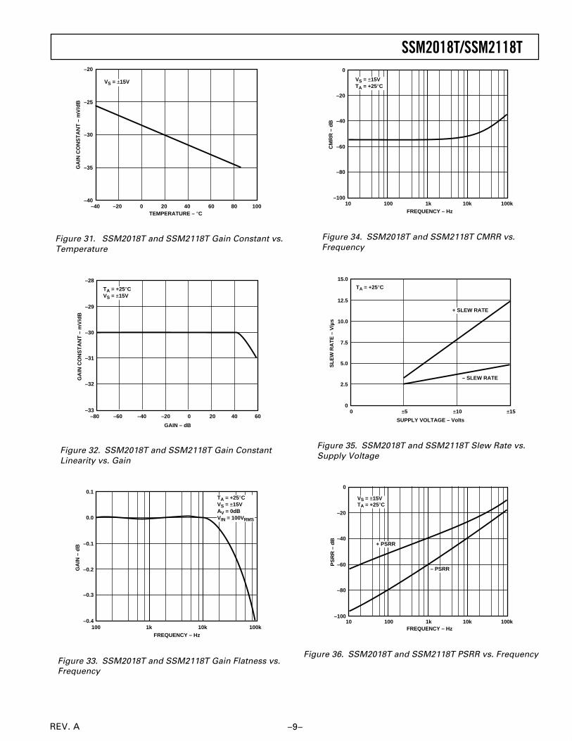
REV. A –9–
SSM2018T/SSM2118T–20
–40–40 100
–25
–35
–20
–30
60 8040200TEMPERATURE – °C
GA
IN C
ON
ST
AN
T –
mV
/dB
VS = ±15V
Figure 31. SSM2018T and SSM2118T Gain Constant vs.
Temperature
–28
–3360
–30
–32
–60
–31
–80
–29
40200–20–40
GAIN – dB
GA
IN C
ON
ST
AN
T –
mV
/dB
TA = +25°CVS = ±15V
Figure 32. SSM2018T and SSM2118T Gain Constant
Linearity vs. Gain
0.1
0.0
–0.4100 1k 100k10k
–0.1
–0.2
–0.3
FREQUENCY – Hz
GA
IN –
dB
TA = +25°CVS = ±15VAV = 0dBVIN = 100VRMS
Figure 33. SSM2018T and SSM2118T Gain Flatness vs.
Frequency
0
–40
–100100 100k10k1k10
–60
–80
–20
FREQUENCY – Hz
CM
RR
– d
B
VS = ±15VTA = +25°C
Figure 34. SSM2018T and SSM2118T CMRR vs.
Frequency
TA = +25°C15.0
0±15
7.5
2.5
±5
5.0
0
12.5
10.0
±10
SUPPLY VOLTAGE – Volts
SL
EW
RA
TE
– V
/µs
+ SLEW RATE
– SLEW RATE
Figure 35. SSM2018T and SSM2118T Slew Rate vs.
Supply Voltage
0
–40
–100100 100k10k1k10
–60
–80
–20
FREQUENCY – Hz
+ PSRR
– PSRR
VS = ±15VTA = +25°C
PS
RR
– d
B
Figure 36. SSM2018T and SSM2118T PSRR vs. Frequency
REV. A–10–
SSM2018T/SSM2118Tto run it in the noninverting single-ended mode. If either inputis unused, the associated 18 kΩ resistor and coupling capacitorshould be removed to prevent any additional noise.
The common-mode rejection in balanced mode is typically55 dB up to 1 kHz, decreasing at higher frequencies as shown inFigure 34. To ensure good CMRR in the balanced configura-tion, the input resistors must be balanced. For example, a 1%mismatch results in a CMRR of 40 dB. To achieve 55 dB,these resistors should have an absolute tolerance match of 0.1%.
The output of the basic VCA is taken from Pin 14, which is theoutput of an internal amplifier. Notice that the second voltageoutput (Pin 16) is connected to the negative supply. This isnormal and actually disables that output amplifier ensuring thatit will not oscillate and cause interference problems. Shortingthe output to the negative supply does not cause the supply cur-rent to increase. This amplifier is only used in the “OVCE” ap-plication explained later.
The control port follows a 30 mV/dB control law. The applica-tion circuit shows a 3 kΩ and 1 kΩ resistor divider from a con-trol voltage. The choice of these resistors is arbitrary and couldbe any values to properly scale the control voltage. In fact, theseresistors could be omitted if the control voltage is already prop-erly scaled. The 1 µF capacitor is in place to provide some fil-tering of the control signal. Although the control feedthrough istrimmed at the factory, the feedthrough increases with fre-quency (Figure 29). Thus, high frequency noise canfeedthrough and add to the noise of the VCA. Filtering thecontrol signal helps minimize this source of noise.
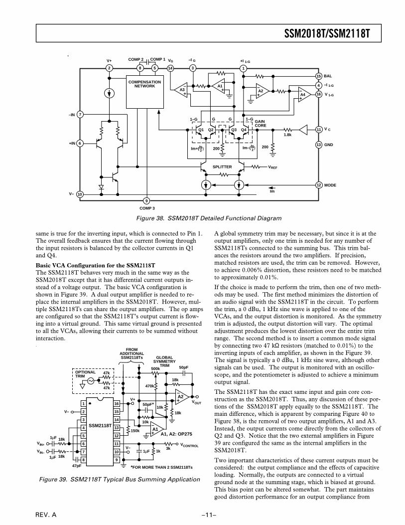
Theory of Operation of the SSM2018TThe SSM2018T has the same internal circuitry as the originalSSM2018. The detailed diagram in Figure 38 shows the maincomponents of the VCA. The essence of the SSM2018T is thegain core, which is comprised of two differential pairs (Q1–Q4).When the control voltage, VC, is adjusted, current through thegain core is steered to one side or the other of the two differen-tial pairs. The tail current for these differential pairs is set bythe mode bias of the VCA (Class A or AB), which is labeled asIM in the diagram. IM is then modulated by a current propor-tional to the input voltage, labeled IS. For a positive input volt-age, more current is steered (by the “Splitter”) to the leftdifferential pair, and the opposite is true for a negative input.
To understand how the gain control works, a simple example isbest. Take the case of a positive control voltage on Pin 11. No-tice that the bases of Q2 and Q3 are connected to ground via a200 Ω resistor. A positive control voltage produces a positivevoltage on the bases of Q1 and Q4. Concentrating on the leftmost differential pair, this raises the base voltage of Q1 abovethat of Q2. Thus, more of the tail current is steered through Q1than through Q2. The current from the collector of Q2 flowsthrough the external 18 kΩ feedback resistor around amplifierA3. When this current is reduced, the output voltage is also re-duced. Thus, a positive control voltage results in an attenuationof the input signal, which explains why the gain constant isnegative.
The collector currents of Q2 and Q3 produce the output volt-age. The output of Q3 is mirrored by amplifier A1 to add to theoverall output voltage. On the other hand, the collector cur-rents of Q1 and Q4 are used for feedback to the differential in-puts. Because Pins 6 and 4 are shorted together, any inputvoltage produces an input current which flows into Pin 4. The
APPLICATIONSThe SSM2018T is a trimless Voltage Controlled Amplifier(VCA) for volume control in audio systems. The SSM2018T isidentical to the original SSM2018 in functionality and pinout;however, it is the first professional quality audio VCAin the marketplace that does not require an external trim-ming potentiometer to minimize distortion. Instead, theSSM2018T is laser trimmed before it is packaged to ensure thespecified THD and control feedthrough performance. This hasa significant savings in not only the cost of external trimmingpotentiometers, but also the manufacturing cost of performingthe trimming during production.
The SSM2118T is identical to the SSM2018T except that dif-ferential current outputs are provided as opposed to a voltageoutput. This output configuration is ideal for bus summing ap-plications where multiple audio signals are summed together.These signals often require long lead lengths or cable runs toreach the summing stage. Transmitting the signals in a differen-tial current mode minimizes the chance for noise pickup and forline impedances to upset the balance of the system. TheSSM2118T is also factory trimmed to minimize distortion andcontrol feedthrough. Thus, no individual trim is required foreach part. One global trim at the summing amplifier stage maybe necessary to properly balance the resistors in this stage, as ex-plained later.
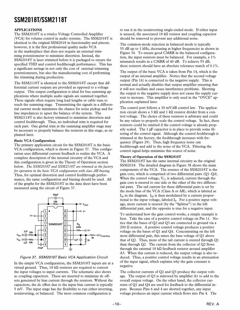
Basic VCA ConfigurationThe primary application circuit for the SSM2018T is the basicVCA configuration, which is shown in Figure 37. This configu-ration uses differential current feedback to realize the VCA. Acomplete description of the internal circuitry of the VCA andthis configuration is given in the Theory of Operation sectionbelow. The SSM2018T and SSM2118T are trimmed at the factoryfor operation in the basic VCA configuration with class AB biasing.Thus, for optimal distortion and control feedthrough perfor-mance, the same configuration and biasing should be used. Allof the graphs for the SSM2018T in the data sheet have beenmeasured using the circuit of Figure 37.
V+1µF
RB150k
18k
V+
18kVIN+
1µF 18kVIN–
47pF
1µF
50pF
1k
VCONTROL3k
VOUT
V–1
2
16
15
5
6
7
12
11
10
3
4
14
13
8 9
SSM2018T
Figure 37. SSM2018T Basic VCA Application Circuit
In the simple VCA configuration, the SSM2018T inputs are at avirtual ground. Thus, 18 kΩ resistors are required to convertthe input voltages to input currents. The schematic also showsac coupling capacitors. These are inserted to minimize dc off-sets generated by bias current through the resistors. Without thecapacitors, the dc offset due to the input bias current is typically5 mV. The input stage has the flexibility to run either inverting,noninverting, or balanced. The most common configuration is
REV. A –11–
SSM2018T/SSM2118T
same is true for the inverting input, which is connected to Pin 1.The overall feedback ensures that the current flowing throughthe input resistors is balanced by the collector currents in Q1and Q4.
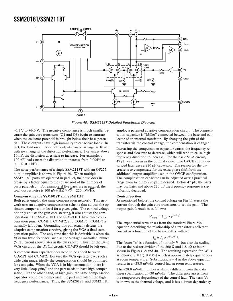
Basic VCA Configuration for the SSM2118TThe SSM2118T behaves very much in the same way as theSSM2018T except that it has differential current outputs in-stead of a voltage output. The basic VCA configuration isshown in Figure 39. A dual output amplifier is needed to re-place the internal amplifiers in the SSM2018T. However, mul-tiple SSM2118Ts can share the output amplifiers. The op ampsare configured so that the SSM2118T’s output current is flow-ing into a virtual ground. This same virtual ground is presentedto all the VCAs, allowing their currents to be summed withoutinteraction.
1µF 18kVIN+
V–
150k A1
10k
10k
18k
18k
500k 50pF
VOUT
GLOBALSYMMETRY
TRIM
FROMADDITIONALSSM2118Ts
V–
1µF 18kVIN–
47pF
1µF3k
VCONTROL
V+50pF*
470k
OPTIONAL TRIM
47k
47k
A1, A2: OP275
1
2
5
6
7
3
4
8
16
15
12
11
10
14
13
9
SSM2118T
A2
1k
*FOR MORE THAN 2 SSM2118Ts
Figure 39. SSM2118T Typical Bus Summing Application
A global symmetry trim may be necessary, but since it is at theoutput amplifiers, only one trim is needed for any number ofSSM2118Ts connected to the summing bus. This trim bal-ances the resistors around the two amplifiers. If precision,matched resistors are used, the trim can be removed. However,to achieve 0.006% distortion, these resistors need to be matchedto approximately 0.01%.
If the choice is made to perform the trim, then one of two meth-ods may be used. The first method minimizes the distortion ofan audio signal with the SSM2118T in the circuit. To performthe trim, a 0 dBu, 1 kHz sine wave is applied to one of theVCAs, and the output distortion is monitored. As the symmetrytrim is adjusted, the output distortion will vary. The optimaladjustment produces the lowest distortion over the entire trimrange. The second method is to insert a common mode signalby connecting two 47 kΩ resistors (matched to 0.01%) to theinverting inputs of each amplifier, as shown in the Figure 39.The signal is typically a 0 dBu, 1 kHz sine wave, although othersignals can be used. The output is monitored with an oscillo-scope, and the potentiometer is adjusted to achieve a minimumoutput signal.
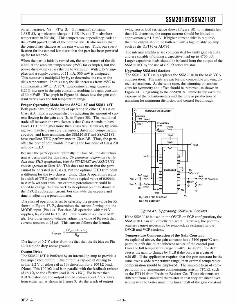
The SSM2118T has the exact same input and gain core con-struction as the SSM2018T. Thus, any discussion of these por-tions of the SSM2018T apply equally to the SSM2118T. Themain difference, which is apparent by comparing Figure 40 toFigure 38, is the removal of two output amplifiers, A1 and A3.Instead, the output currents come directly from the collectors ofQ2 and Q3. Notice that the two external amplifiers in Figure39 are configured the same as the internal amplifiers in theSSM2018T.
Two important characteristics of these current outputs must beconsidered: the output compliance and the effects of capacitiveloading. Normally, the outputs are connected to a virtualground node at the summing stage, which is biased at ground.This bias point can be altered somewhat. The part maintainsgood distortion performance for an output compliance from
A4
Q3 Q4Q1 Q2
200
1–G GG 1–G
200
1.8k
GAINCORE
148 52
COMP 1
COMPENSATIONNETWORK
9
VREF
Im
SPLITTER
A1A3
VG +I 1-G
3 1
15
4
16
11
13
12
BAL
–I 1-G
V 1-G
V C
GND
MODE
–I G
COMP 3
COMP 2V+
7
6
10V–
+IN
–IN
Im+(Is)2Im–(Is)
2
A2A4
Figure 38. SSM2018T Detailed Functional Diagram
REV. A–12–
SSM2018T/SSM2118T
A2A4
Q3 Q4Q1 Q2
200
1–G GG 1–G
200
1.8k
GAINCORE
148 5
16
COMP 2 COMP 1
9
VREF
Im
SPLITTER
+IG
3
1
15
4
2
11
13
12
BAL
–I1–G
V1–G
VC
GND
MODE
–IG
COMP 3
7
6
10V–
+IN
–IN
+I1–G
V+COMPENSATION
NETWORK
Im–(Is)2Im+(Is)
2
A4
–0.1 V to +6.0 V. The negative compliance is much smaller be-cause the gain core transistors (Q1 and Q3) begin to saturatewhen the collector potential is brought below their base poten-tial. These outputs have high immunity to capacitive loads. Infact, the load on either or both outputs can be as large as 10 nFwith no change in the distortion performance. For values above10 nF, the distortion does start to increase. For example, a100 nF load causes the distortion to increase from 0.006% to0.02% at 1 kHz.
The noise performance of a single SSM2118T with an OP275output amplifier is shown in Figure 20. When multipleSSM2118T parts are operated in parallel, the noise does in-crease by a factor equal to the square root of the number ofparts paralleled. For example, if five parts are in parallel, thetotal output noise is 100 nV√(Hz) × √5 = 220 nV/√Hz.
Compensating the SSM2018T and SSM2118TBoth parts employ the same compensation network. This net-work uses an adaptive compensation scheme that adjusts the op-timum compensation level for a given gain. The control voltagenot only adjusts the gain core steering, it also adjusts the com-pensation. The SSM2018T and SSM2118T have three com-pensation pins: COMP1, COMP2, and COMP3. COMP3 isnormally left open. Grounding this pin actually defeats theadaptive compensation circuitry, giving the VCA a fixed com-pensation point. The only time that this is desirable is when theVCA has fixed feedback, such as the Voltage Controlled Panner(VCP) circuit shown later in the data sheet. Thus, for the BasicVCA circuit or the OVCE circuit, COMP3 should be left open.
A compensation capacitor does need to be added betweenCOMP1 and COMP2. Because the VCA operates over such awide gain range, ideally the compensation should be optimizedfor each gain. When the VCA is in high attenuation, there isvery little “loop gain,” and the part needs to have high compen-sation. On the other hand, at high gain, the same compensationcapacitor would overcompensate the part and roll off the highfrequency performance. Thus, the SSM2018T and SSM2118T
employ a patented adaptive compensation circuit. The compen-sation capacitor is “Miller” connected between the base and col-lector of an internal transistor. By changing the gain of thistransistor via the control voltage, the compensation is changed.
Increasing the compensation capacitor causes the frequency re-sponse and slew rate to decrease, which will tend to cause highfrequency distortion to increase. For the basic VCA circuit,47 pF was chosen as the optimal value. The OVCE circuit de-scribed later uses a 220 pF capacitor. The reason for the in-crease is to compensate for the extra phase shift from theadditional output amplifier used in the OVCE configuration.The compensation capacitor can be adjusted over a practicalrange from 47 pF to 220 pF, if desired. Below 47 pF, the partsmay oscillate, and above 220 pF the frequency response is sig-nificantly degraded.
Control SectionAs mentioned before, the control voltage on Pin 11 steers thecurrent through the gain core transistors to set the gain. Theoutput gain formula is as follows:
V OUT = V IN × e(–aVC )
The exponential term arises from the standard Ebers-Mollequation describing the relationship of a transistor’s collectorcurrent as a function of the base-emitter voltage:
IC = IS × e(V BE /VT ).
The factor “a” is a function of not only VT but also the scalingdue to the resistor divider of the 200 Ω and 1.8 kΩ resistorsshown in Figures 38 and 40. The resulting expression for “a” isas follows: a = 1/(10 × VT) which is approximately equal to fourat room temperature. Substituting a = 4 in the above equationresults in a –28.8 mV/dB control law at room temperature.
The –28.8 mV/dB number is slightly different from the datasheet specification of –30 mV/dB. The difference arises fromthe temperature dependency of the control law. The term VT
is known as the thermal voltage, and it has a direct dependency
Figure 40. SSM2118T Detailed Functional Diagram
REV. A –13–
SSM2018T/SSM2118Ton temperature: VT = kT/q (k = Boltzmann’s constant =1.38E-23, q = electron charge = 1.6E-19, and T = absolutetemperature in Kelvin). This temperature dependency leads tothe –3500 ppm/°C drift of the control law. It also means thatthe control law changes as the part warms up. Thus, our speci-fication for the control law states that the part has been poweredup for 60 seconds.
When the part is initially turned on, the temperature of the dieis still at the ambient temperature (25°C for example), but thepower dissipation causes the die to warm up. With ±15 V sup-plies and a supply current of 11 mA, 330 mW is dissipated.This number is multiplied by θJA to determine the rise in thedie’s temperature. In this case, the die increases from 25°C toapproximately 50°C. A 25°C temperature change causes a8.25% increase in the gain constant, resulting in a gain constantof 30 mV/dB. The graph in Figure 31 shows how the gain con-stant varies over the full temperature range.
Proper Operating Mode for the SSM2018T and SSM2118TBoth parts have the flexibility of operating in either Class A orClass AB. This is accomplished by adjusting the amount of cur-rent flowing in the gain core (IM in Figure 38). The traditionaltrade-off between the two classes is that Class A tends to havelower THD but higher noise than Class AB. However, by utiliz-ing well matched gain core transistors, distortion compensationcircuitry, and laser trimming, the SSM2018T and SSM2118Thave excellent THD performance in Class AB. Thus, the partsoffer the best of both worlds in having the low noise of Class ABwith low THD.
Because the parts operate optimally in Class AB, the distortiontrim is performed for this class. To guarantee conformance to thedata sheet THD specifications, both the SSM2018T and SSM2118Tmust be operated in Class AB. This does not mean that the partscannot be operated in Class A, but the optimal THD trim pointis different for the two classes. Using Class A operation resultsin a shift of THD performance from a typical value of 0.006%to 0.05% without trim. An external potentiometer could beadded to change the trim back to its optimal point as shown inthe OVCE application circuit, but this adds the expense andtime in adjusting a potentiometer.
The class of operation is set by selecting the proper value for RB
shown in Figure 37. RB determines the current flowing into theMODE input (Pin 12). For class AB operation with ±15 Vsupplies, RB should be 150 kΩ. This results in a current of 95µA. For other supply voltages, adjust the value of RB such thatcurrent remains at 95 µA. This current follows the formula:
IMODE = (VCC – 0.7V )
RB
The factor of 0.7 V arises from the fact that the dc bias on Pin12 is a diode drop above ground.
Output DriveThe SSM2018T is buffered by an internal op amp to provide alow impedance output. This output is capable of driving towithin 1.2 V of either rail at 1% distortion for a 100 kΩ load.(Note: This 100 kΩ load is in parallel with the feedback resistorof 18 kΩ, so the effective load is 15.3 kΩ.) For better than0.01% distortion, the output should remain about 3.5 V awayfrom either rail as shown in Figure 3. As the graph of output
swing versus load resistance shows (Figure 10), to maintain lessthan 1% distortion, the output current should be limited toapproximately ±1.3 mA. If higher current drive is required,then the output should be buffered with a high quality op ampsuch as the OP176 or AD797.
The internal amplifiers are compensated for unity gain stabilityand are capable of driving a capacitive load up to 4700 pF.Larger capacitive loads should be isolated from the output of theSSM2018T by the use of a 50 Ω series resistor.
Upgrading SSM2018 SocketsThe SSM2018T easily replaces the SSM2018 in the basic VCAconfiguration. The parts are pin for pin compatible allowing di-rect replacement. At the same time, the trimming potentiom-eters for symmetry and offset should be removed, as shown inFigure 41. Upgrading to the SSM2018T immediately saves theexpense of the potentiometers and the time in production oftrimming for minimum distortion and control feedthrough.
18kΩ
50pF
V+
VOUT
47pFNC
1µF1kΩ
3kΩ
V–
V+1µF 18kΩ
1µF 18kΩ
RB: 150kΩ FOR CLASS AB
NC = NO CONNECT
RB
VCONTROLVIN+
VIN–
1
2
3
4
5
6
7
8
16
15
14
13
12
10
9
SSM2018T
11
470kΩ
500kΩ
100kΩ
10MΩOFFSETTRIM
V+
V–
SYMMETRYTRIM
REMOVE FOR SSM2018T
Figure 41. Upgrading SSM2018 Sockets
If the SSM2018 is used in the OVCE or VCP configuration, theSSM2018T can still directly replace it. However, the potenti-ometers cannot necessarily be removed, as explained in theOVCE and VCP sections.
Temperature Compensation of the Gain ConstantAs explained above, the gain constant has a 3500 ppm/°C tem-perature drift due to the inherent nature of the control port.Over the full temperature range of –40°C to +85°C, the driftcauses the gain to change by 7 dB if the part is in a gain of±20 dB. If the application requires that the gain constant be thesame over a wide temperature range, then external temperaturecompensation should be employed. The simplest form of com-pensation is a temperature compensating resistor (TCR), suchas the PT146 from Precision Resistor Co. These elements aredifferent from a standard thermistor in that they are linear overtemperature to better match the linear drift of the gain constant.
REV. A–14–
SSM2018T/SSM2118Tsuch that full scale produces 80 dB of attenuation. The resistordivider can be adjusted to provide other attenuation ranges. If aparallel interface is needed, then the DAC8562 may be used, orfor a dual DAC, the AD8582.
0.1µF
+15V
18kΩVIN
6DAC8512 8
7
CS
CLR
2
1
0.1µF
18kΩ
50pF
47pF
VOUT
150kΩ+15V
–15V
0.1µF
+5V
CCON
1µF
R6825Ω
R71kΩ
0V ≤ VC ≤ +2.24V
5LD
3SCLK
4SDI
1
2
3
4
5
6
7
8
16
15
14
13
12
11
10
9
SSM2018T
NC
NC
NC
NC
NC = NO CONNECT
Figure 44. 12-Bit DAC Controls the VCA Gain
Supply Considerations and Single Supply OperationThe SSM2018T and SSM2118T have a wide operating supplyrange. Many of the graphs in this data sheet show the perfor-mance of the part from ±5 V to ±18 V. These graphs offer typi-cal performance specifications and are a good indication of theparts capabilities. The minimum operating supply voltage is±4.5 V. Below this voltage, the parts are inoperable. Thus, toaccount for supply variations, the recommended minimum sup-ply is ±5 V.
The circuits in the data sheet do not show supply decoupling forsimplicity; however, to ensure best performance, each supplypin should be decoupled with a 0.1 µF ceramic (or other low re-sistance and inductance type) capacitor as close to the packageas possible. This minimizes the chance of supply noise feedingthrough the part and causing excessive noise in the audio fre-quency range.
The SSM2018T and SSM2118T can be operated in single sup-ply mode as long as the circuit is properly biased. Figure 45shows the proper configuration, which includes an amplifier tocreate a false ground node midway between the supplies. Ahigh quality, wide bandwidth audio amplifier such as the OP176or AD797 should be used to ensure a very low impedanceground over the full audio frequency range. The minimum op-erating supply for the SSM2018 is ±5 V, which gives a mini-mum single supply of +10 V and ground. The performance ofthe circuit with +10 V is identical to graphs that show operationof the SSM2018T with ±5 V supplies.
1µF
2kΩVC (PIN 11)
SSM2018T OR SSM2118T1kΩ*3500ppm/°C
1kΩ*3500ppm/°C
CONTROLVOLTAGE
*PRECISION RESISTOR CO.10601 75TH ST. NORTHLARGO, FL 34647(813) 541-5771
Figure 42. Two TCRs Compensate for Temperature Drift
of Gain Constant
+15V
–15V
R3
10kΩ
50pF
R41kΩ
R5
9kΩ
R1
10kΩ
OP176
R210kΩ
1kΩ*3500ppm/°C
VC (PIN 11)SSM2018T OR SSM2118T
CONTROLVOLTAGE
Figure 43. Current Source Allows Temperature Compen-
sation with One TCR
One of the resistors in the divider to the control port can be sub-stituted with an appropriately chosen TCR to compensate theSSM2018T or the SSM2118T as shown in Figure 42. Becausethe resistor divider effectively cuts the temperature coefficient inhalf, two TCRs must be used. The combined drift of the two is7000 ppm/°C, given an effective drift for to the control voltageof –3500 ppm/°C. Of course, a single TCR with the appropriatecoefficient can be used. The 3500 ppm parts were chosen be-cause they are a standard item and do not need to be specialordered.
In many applications, an op amp is used to drive the controlvoltage. If this is the case, it may be more economical to use theop amp and a single TCR for temperature compensation. Theop amp is configured as a Howland current source as shown inFigure 43. The current then flows through a single TCR tocreate the control voltage. Because the resistor divider is notpresent, the temp coefficient is equivalent to the TCR’s coef-ficient. Using this technique, the drift was reduced from–3500 ppm/°C to –150 ppm/°C, which results in a total com-pensated gain shift of 0.4 dB over the full temperature range at again of ±20 dB.
Digital Control of the GainA common method of controlling the gain of a VCA is to use adigital-to-analog converter to set the control voltage. Figure 44shows a 12-bit DAC, the DAC8512, controlling the SSM2018T(or SSM2118T). The DAC8512 is a complete 12-bit converterin an 8-pin package. It includes an on board reference and aoutput amplifier to produce an output voltage from 0 V to+4.095 V, which is 1 mV/bit. Since the voltage is always posi-tive, this circuit only provides attenuation. The resistor divideron the output of the DAC8512 is set to scale the output voltage
REV. A –15–
SSM2018T/SSM2118T
V+1µF
RB
18k
V+
18kVIN+
1µF 18kVIN–
47pF
1µF
50pF
1k
VCONTROL3k
VOUT
1
2
16
15
5
6
7
12
11
10
3
4
14
13
8 9
SSM2018T
V+
OP176
100k
100k
V+
10µF
Figure 45. Single Supply Operation of SSM2018T
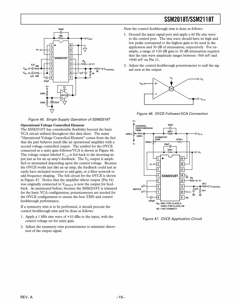
Operational Voltage Controlled ElementThe SSM2018T has considerable flexibility beyond the basicVCA circuit utilized throughout this data sheet. The name“Operational Voltage Controlled Element” comes from the factthat the part behaves much like an operational amplifier with asecond voltage controlled output. The symbol for the OVCEconnected as a unity gain follower/VCA is shown in Figure 46.The voltage output labeled V1–G is fed back to the inverting in-put just as for an op amp’s feedback. The VG output is ampli-fied or attenuated depending upon the control voltage. Becausethe OVCE works just like an op amp, the feedback could just aseasily have included resistors to add gain, or a filter network toadd frequency shaping. The full circuit for the OVCE is shownin Figure 47. Notice that the amplifier whose output (Pin 16)was originally connected to VMINUS is now the output for feed-back. As mentioned before, because the SSM2018T is trimmedfor the basic VCA configuration, potentiometers are needed forthe OVCE configuration to ensure the best THD and controlfeedthrough performance.
If a symmetry trim is to be performed, it should precede thecontrol feedthrough trim and be done as follows:
1. Apply a 1 kHz sine wave of +10 dBu to the input, with thecontrol voltage set for unity gain.
2. Adjust the symmetry trim potentiometer to minimize distor-tion of the output signal.
Next the control feedthrough trim is done as follows:
1. Ground the input signal port and apply a 60 Hz sine waveto the control port. The sine wave should have its high andlow peaks correspond to the highest gain to be used in theapplication and 30 dB of attenuation, respectively. For ex-ample, a range of +20 dB gain to 30 dB attenuation requiresthat the sine wave amplitude ranges between –560 mV and+840 mV on Pin 11.
2. Adjust the control feedthrough potentiometer to null the sig-nal seen at the output.
VIN
VC VG
V1–G
Figure 46. OVCE Follower/VCA Connection
18kΩ
50pF
470kΩ500kΩ
V+
100kΩ10MΩ
CONTROLFEEDTHROUGHTRIM
V+
V–
V1–G
VG
INPUTS
220pFNC
V–
1µF1kΩ
3kΩVCONTROL
RB: 30kΩ FOR CLASS A 150kΩ FOR CLASS ABNC = NO CONNECT
SYMMETRYTRIM
V+RB
1
2
3
4
5
6
7
8
16
15
14
13
12
11
10
9
SSM2018T
18kΩ
50pF
Figure 47. OVCE Application Circuit
REV. A–16–
SSM2018T/SSM2118T
PR
INT
ED
IN
U.S
.A.
C1
93
7–5
–7
/94
OUTLINE DIMENSIONSDimensions shown in inches and (mm).
16-Pin Plastic DIP (N-16) Package
PIN 10.280 (7.11)0.240 (6.10)
916
1 8
0.210(5.33)MAX
0.160 (4.06)0.115 (2.93)
0.022 (0.558)0.014 (0.356)
0.100 (2.54)BSC
SEATINGPLANE
0.060 (1.52)0.015 (0.38)
0.130(3.30)MIN
0.070 (1.77)0.045 (1.15)
0.840 (21.33)0.745 (18.93)
0.325 (8.25)0.300 (7.62)
0.015 (0.381)0.008 (0.204)
0.195 (4.95)0.115 (2.93)
16-Pin SOIC (R-16) Package
PIN 1
0.2992 (7.60)0.2914 (7.40)
0.4193 (10.65)0.3937 (10.00)
1
16 9
8
0.0192 (0.49)0.0138 (0.35)
0.0500 (1.27)BSC
0.1043 (2.65)0.0926 (2.35)
0.4133 (10.50) 0.3977 (10.00)
0.0118 (0.30)0.0040 (0.10)
0.0500 (1.27)0.0157 (0.40)
8°0°
0.0291 (0.74)0.0098 (0.25)
x 45°
0.0125 (0.32)0.0091 (0.23)
Voltage Controlled PannerAn interesting circuit that is built with the OVCE building blockis a voltage controlled panner. Figure 48 shows the feedbackconnection for the circuit. Notice that the average of both out-puts is fed back to the input. Thus, the average must be equalto the input voltage. When the control voltage is set for gain atVG, this causes V1-G to attenuate (to keep the average the same).On the other hand, when VG is attenuated, V1-G is amplified.The result is that the control voltage causes the input to “pan”from one output to the other. The following expressions showhow this circuit works mathematically:
VG = 2 K ×V IN and V I –G = 2(1– K )×V IN
where K varies between 0 and 1 as the control voltage ischanged from full attenuation to full gain respectively. WhenVC = 0, then K = 0.5 and VG = V1-G = VIN. Again, trimming isrequired for best performance. Pin 9 should be grounded. Thisis possible because the feedback is constant and the adaptivenetwork is not needed. The VCP is the only application shownin this data sheet where Pin 9 is grounded.
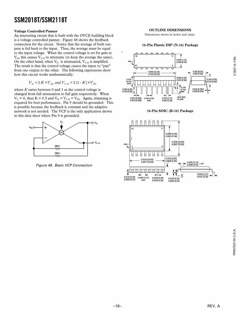
VIN
VC VG
V1–G
18kΩ
18kΩ
Figure 48. Basic VCP Connection