Embed Size (px)
Citation preview
This is an electronic reprint of the original article.This reprint may differ from the original in pagination and typographic detail.
Powered by TCPDF (www.tcpdf.org)
This material is protected by copyright and other intellectual property rights, and duplication or sale of all or part of any of the repository collections is not permitted, except that material may be duplicated by you for your research use or educational purposes in electronic or print form. You must obtain permission for any other use. Electronic or print copies may not be offered, whether for sale or otherwise to anyone who is not an authorised user.
Sharma, Vishal; Vishvakarma, Santosh; Chouhan, Shailesh Singh; Halonen, KariA write-improved low-power 12T SRAM cell for wearable wireless sensor nodes
Published in:International Journal of Circuit Theory and Applications
DOI:10.1002/cta.2555
Published: 01/12/2018
Document VersionPeer reviewed version
Please cite the original version:Sharma, V., Vishvakarma, S., Chouhan, S. S., & Halonen, K. (2018). A write-improved low-power 12T SRAMcell for wearable wireless sensor nodes. International Journal of Circuit Theory and Applications, 46(12), 2314-2333. https://doi.org/10.1002/cta.2555
Received: 26 December 2017 Revised: 16 May 2018 Accepted: 23 July 2018
DOI: 10.1002/cta.2555
R E S E A R C H A R T I C L E
A write-improved low-power 12T SRAM cell for wearablewireless sensor nodes
Vishal Sharma1 Santosh Vishvakarma1 Shailesh Singh Chouhan2 Kari Halonen3
1Nanoscale Devices, VLSI Circuit &System Design Lab, Department ofElectrical Engineering, Indian Institute ofTechnology, Indore, India2EISLAB, Department of ComputerScience, Electrical and Space Engineering,Lulea University of Technology, Lulea,Sweden3Electronic Circuit Design Lab,Department of Electronics and NanoEngineering, Aalto University, Espoo,Finland
CorrespondenceSantosh Vishvakarma, Nanoscale Devices,VLSI Circuit & System Design Lab,Department of Electrical Engineering,Indian Institute of Technology, Indore, MP453552, India.Email: [email protected]
Funding informationCenter for International Mobility (CIMO),Grant/Award Number: Intia-1-2016-03;Aalto University, Finland; SpecialManpower Development Program forChips to System Design (SMDP-C2SD)
Summary
In this work, a data-dependent feedback-cutting–based bit-interleaved 12T staticrandom access memory (SRAM) cell is proposed, which enhances the write mar-gin in terms of write trip point (WTP) and write static noise margin (WSNM) by2.14× and 8.99× whereas read stability in terms of dynamic read noise margin(DRNM) and read static noise margin (RSNM) by 1.06× and 2.6 ×, respectively,for 0.4 V when compared with a conventional 6T SRAM cell. The standby powerhas also been reduced to 0.93× with an area overhead of 1.49× as that of 6T.Monte Carlo simulation results show that the proposed cell offers a robust writemargin when compared with the state-of-the-art memory cells available in theliterature. An analytical model of WSNM for 12T operating in subthresholdregion is also proposed, which has been verified using the simulation results.Finally, a small SRAM macro along with its independent memory controller hasbeen designed.
KEYWORDS
circuit design, low-power, SRAM, stability, write ability
1 INTRODUCTION
With the aggressive growth of semiconductor market, the usage of on-site static random access memory (SRAM) is alsoincreasing. The key design parameters for SRAM, which needs to be improved, vary according to its applications. Forexample, Internet of Things (IoTs), body sensor nodes (BSNs), wearable electronics, and image processing applicationsdemand robustness and energy efficiency1; while for recent artificial neural networks (ANNs) applications, graphics(GPU) processors, servers, and other high end applications, the energy is traded off to achieve high performance.2 More-over, in case of wearable IoT applications (such as Google Glass, Fitbit, and Pebble), detecting and reacting to the mobileand ambient context (like speech, occupancy, and motion) from the wireless IoT sensor data has been the key enablerof research. All of these sensors capture and analyze the run time data by temporarily storing it into a memory, andthus, SRAM has been the repetitive architecture of this data storage and occupies the major portion of the system area.3
Therefore, the power consumed by SRAM plays the crucial role in overall power consumed by the system.Various methods have been implemented in the literature for minimizing the power consumption in which the voltage
scaling has always been the preferred choice to reduce both the switching and leakage power for CMOS VLSI.4 How-ever, designing a resilient SRAM operating in near-threshold or subthreshold region is extremely challenging due to the
Int J Circ Theor Appl. 2018;1–20. wileyonlinelibrary.com/journal/cta © 2018 John Wiley & Sons, Ltd. 1
2 SHARMA ET AL.
increased effect of process, voltage, and temperature (PVT) variations.5 Therefore, the use of conventional 6T SRAM cell ata low-supply voltage (< 2VTH) operation is not preferable due to the reduced noise margin, which leads towards a higherprobability of the cell malfunctioning.6 Read disturb, half-select destruction, and read-write conflict are other major issuesof conventional 6T cell at low-supply voltage.
Moreover, in order to implement a large on-chip functionality, the designs are migrating towards the advanced technol-ogy nodes. However, with these decreasing technology nodes, the memory failure probability is increasing.7 To addressthese issues, various bit cells have been proposed. Verma and Chandrakasan8 and Kim et al9 proposed an approach toremove read disturbance and thus to improve the read static noise margin (RSNM) of SRAM cells by decoupling the stor-age nodes from the bit lines, which is termed as read decoupling. However, any effective strategy to improve the writeability was absent in this solution. Static random access memory cells in Chang et al10 and Kushwah and Vishvakarma11
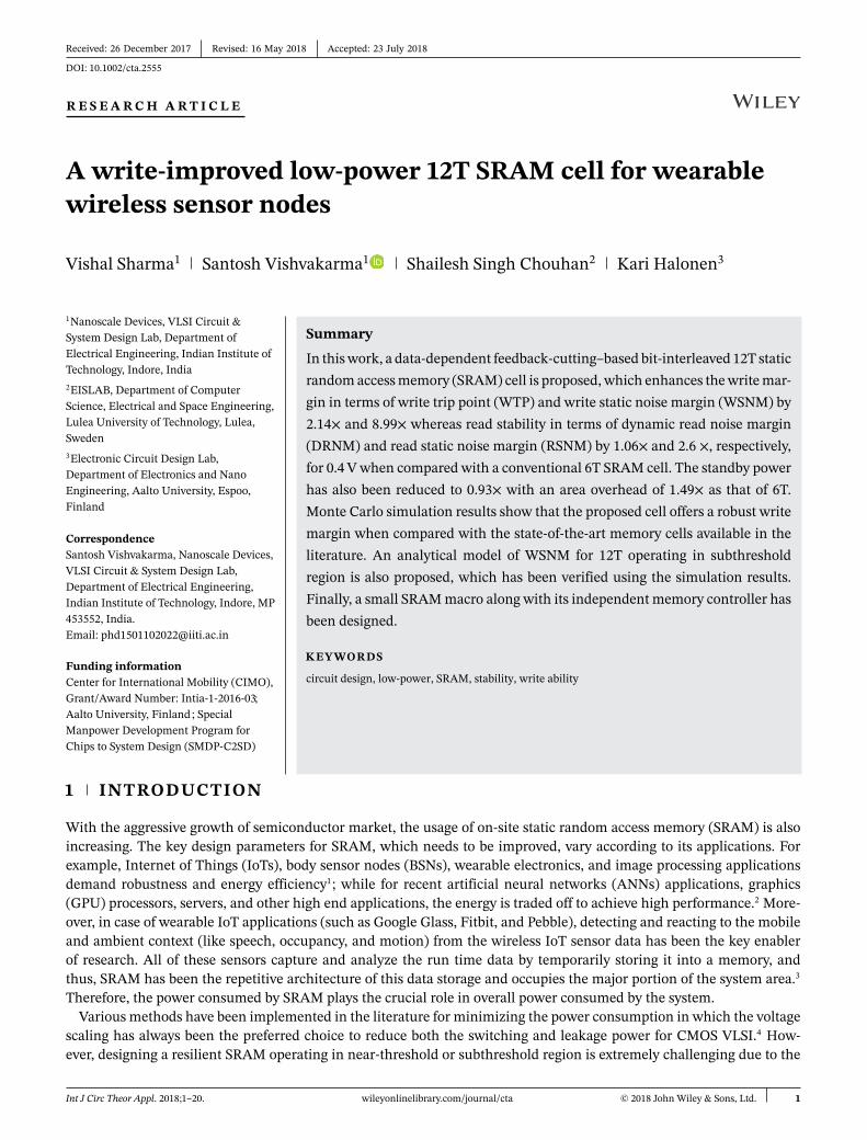
proposed the feedback-cutting–based methodology for the inverter pair used in SRAM to enhance the write margin anddynamic read decoupling to reduce the read disturb. A provision to reduce the leakage power was also incorporatedwhereby the stacking devices in each of the inverter. However, feedback cutting through NMOS devices causes the stor-age nodes to be floating. Hence, the cells become prone towards the leakage current and noise occurrence.5 In addition,these implementations also demand for additional circuitry to generate the data-dependent control signals. A PPN10Tcell designed in Lo and Huang12 uses a latch formed by a cross coupled P-P-N inverter pair for ultralow cell leakage andhigh immunity to data-dependent bit-line leakage. However, the cell has lower write ability. Saeidi et al13 proposed a dif-ferential 8T cell by cutting off the feedback loop of the cell during read operation and thus to expand the read margin.But it required the use of wider access devices for improved write ability, and therefore, results in the area overhead. InMoghaddam et al,14 a 9T cell was proposed that is based on the threshold voltage variation technique, where the dynamicthreshold voltage (VTH) effect and drain-induced barrier lowering (DIBL) concepts were implemented to suppress theleakage issues. Wang et al15 proposed a method for energy efficient SRAM cell by the strategic use of multi-VTH devices.But it demands for an additional boosted supply and also involved extra processing steps during fabrication. In Maroofet al,16 a 10T cell using the charge sharing mechanism between the bit lines has been proposed, which avoids the needof bit line to be precharged up to complete VDD voltage. It results in the improved low-power memory cell, but there isno specific strategy incorporated to improve the write stability. The half-select issues are also not addressed by the work.Therefore, all of the aforementioned discussed cells either contributed to improve the read stability or to control the leak-age power. In practice, along with the leakage reduction and read data stability, write ability of SRAM is equally importantfor the present wearable and mobile IoT systems to record and process the data successfully. Figure 1 shows differentpublished cells, which have been considered in this work.
The work published in Chiu et al5 proposed a 12T SRAM cell, which has incorporated the data-aware power-cutoffscheme to improve the write operation at low-supply voltage. But the use of two data-dependent word line signal of thecell demands an additional signal generating circuitry, which has resulted into the area and power overhead for the overallmemory array. Another single write port bit cell based on cutting off the supply voltage to improve the write ability wasproposed in Jain et al.17 But the power cutoff is recovered back once the current write clock cycle is completed, and hence,the written data may be disturbed by the noise interference during the next clock transition. In Kim and Mazumder,18
another 12T memory cell has been proposed for write margin improvement. However, no consideration for the impact ofmemory half-select issues has been made.
In this work, we propose a new cross-point selection based 12T SRAM memory cell. The contributions of this work canbe summarized as follows:
1) Stacked combination incorporated with the pull down networks of inverter pair, controlled by the bit lines, supportsto enhance the write ability, and thus enlarges the write noise margin.
(D) (A) (B) (C)
FIGURE 1 Published SRAM bitcell structures from literature. A, conventional 6T; B, PPN10T12; C, DAWA12T5; and D, 12T J.Kim.18 RWL,read word line; SRAM, static random access memory; WL, word line; WWL, write word line
SHARMA ET AL. 3
2) Isolated read path of proposed cell removes the probability of any noise occurrence and thus produces the readstability in terms of RSNM equivalent to that of hold SNM (HSNM).
3) Column-wise selection through additional NMOS in the write access path enables bit-interleaving structure andcompletely solves the half-select issues during write operation.
4) Stacking effect in cross-coupled inverters reduces the leakage power.5) The proposed cell demonstrates its robustness towards the PVT variations.6) A small size (256 bits) memory with its independent controller has been designed and implemented in a standard
180-nm technology.
Rest of this paper is organized as follows: In section 2, we discuss the proposed 12T SRAM cell and its operation com-paring the post-layout simulation results with the state-of-the-art memory cells. Also, we propose an analytical modelingfor the write static noise margin (WSNM) of the proposed cell when operating in subthreshold region. Then after, thedesign and analysis of memory array is discussed in section 3. Section 4 concludes the paper.
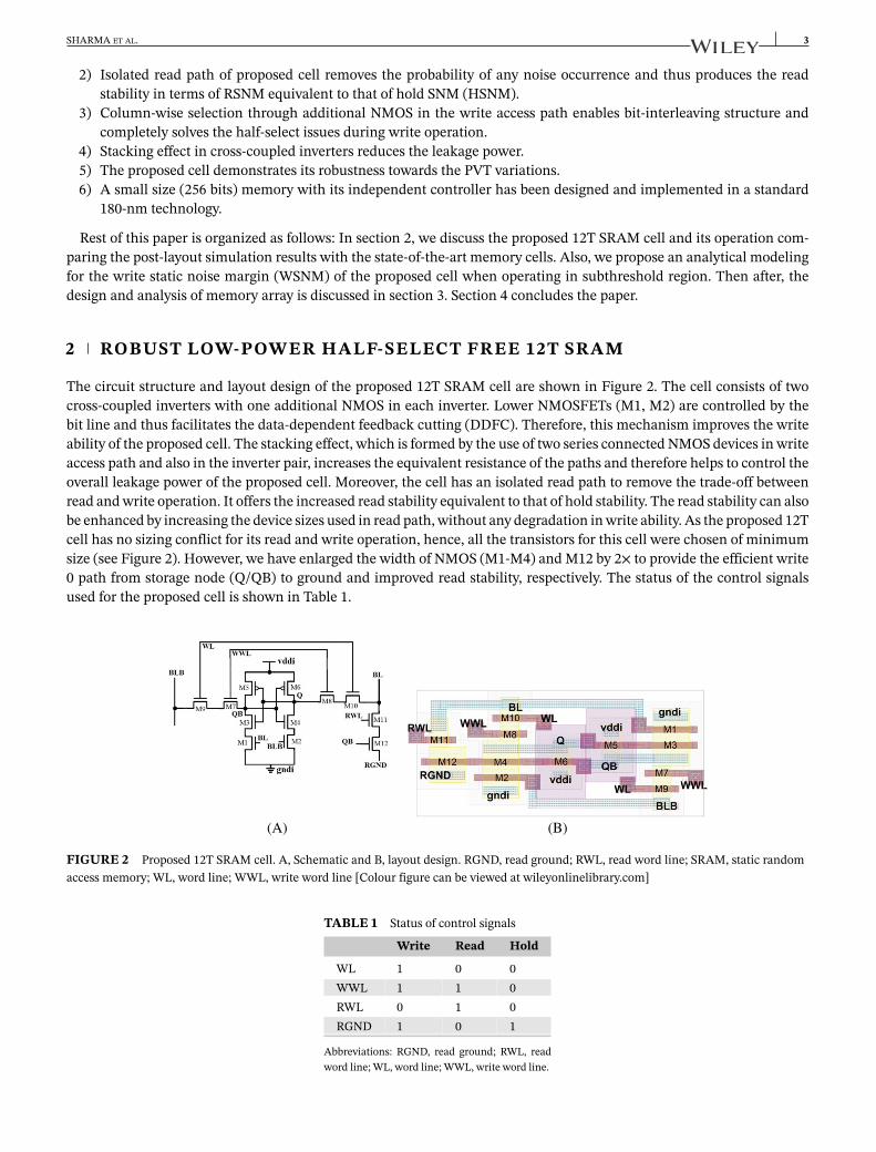
2 ROBUST LOW-POWER HALF-SELECT FREE 12T SRAM
The circuit structure and layout design of the proposed 12T SRAM cell are shown in Figure 2. The cell consists of twocross-coupled inverters with one additional NMOS in each inverter. Lower NMOSFETs (M1, M2) are controlled by thebit line and thus facilitates the data-dependent feedback cutting (DDFC). Therefore, this mechanism improves the writeability of the proposed cell. The stacking effect, which is formed by the use of two series connected NMOS devices in writeaccess path and also in the inverter pair, increases the equivalent resistance of the paths and therefore helps to control theoverall leakage power of the proposed cell. Moreover, the cell has an isolated read path to remove the trade-off betweenread and write operation. It offers the increased read stability equivalent to that of hold stability. The read stability can alsobe enhanced by increasing the device sizes used in read path, without any degradation in write ability. As the proposed 12Tcell has no sizing conflict for its read and write operation, hence, all the transistors for this cell were chosen of minimumsize (see Figure 2). However, we have enlarged the width of NMOS (M1-M4) and M12 by 2× to provide the efficient write0 path from storage node (Q/QB) to ground and improved read stability, respectively. The status of the control signalsused for the proposed cell is shown in Table 1.
(B) (A)
FIGURE 2 Proposed 12T SRAM cell. A, Schematic and B, layout design. RGND, read ground; RWL, read word line; SRAM, static randomaccess memory; WL, word line; WWL, write word line [Colour figure can be viewed at wileyonlinelibrary.com]
TABLE 1 Status of control signals
Write Read Hold
WL 1 0 0WWL 1 1 0RWL 0 1 0RGND 1 0 1
Abbreviations: RGND, read ground; RWL, readword line; WL, word line; WWL, write word line.
4 SHARMA ET AL.
To evaluate the performance of proposed 12T SRAM cell, we have chosen state-of-the-art SRAM cells from the lit-erature those that share the similar implementation strategy and compared the proposed 12T with those cells. All thestate-of–the-art SRAM cells considered in this work have been redesigned as per the information provided in the relatedresearch papers.5,12,18 Table 2 provides the structural comparison of different SRAM cells.
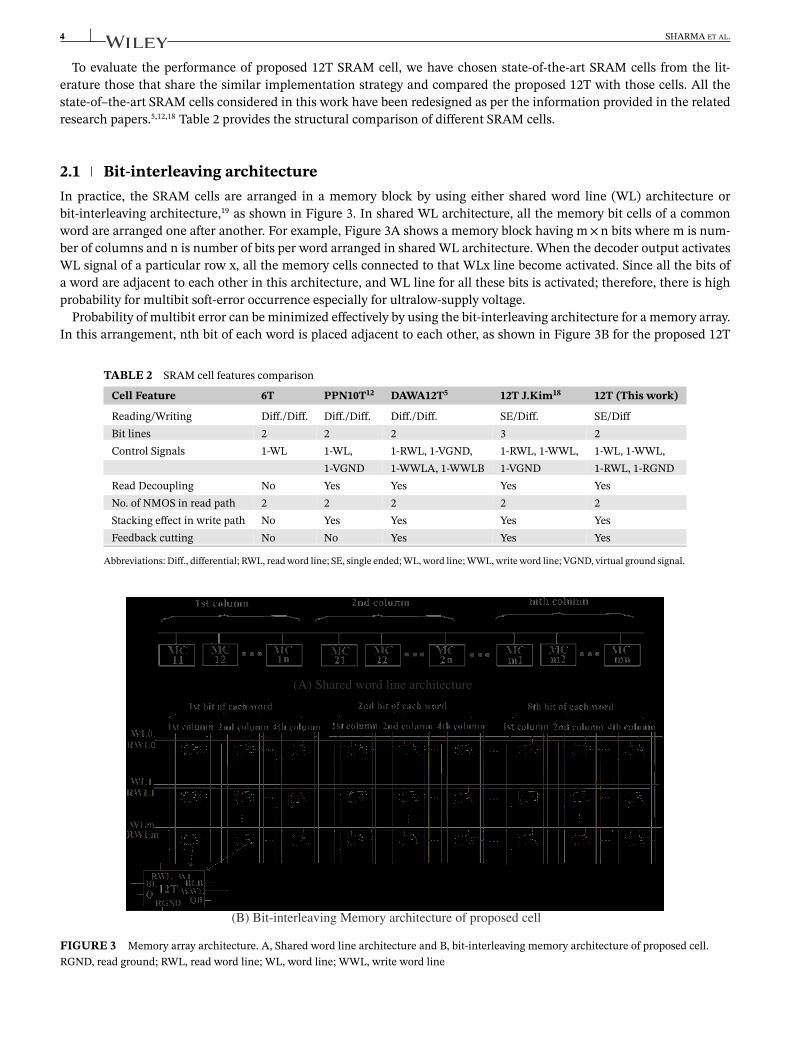
2.1 Bit-interleaving architectureIn practice, the SRAM cells are arranged in a memory block by using either shared word line (WL) architecture orbit-interleaving architecture,19 as shown in Figure 3. In shared WL architecture, all the memory bit cells of a commonword are arranged one after another. For example, Figure 3A shows a memory block having m×n bits where m is num-ber of columns and n is number of bits per word arranged in shared WL architecture. When the decoder output activatesWL signal of a particular row x, all the memory cells connected to that WLx line become activated. Since all the bits ofa word are adjacent to each other in this architecture, and WL line for all these bits is activated; therefore, there is highprobability for multibit soft-error occurrence especially for ultralow-supply voltage.
Probability of multibit error can be minimized effectively by using the bit-interleaving architecture for a memory array.In this arrangement, nth bit of each word is placed adjacent to each other, as shown in Figure 3B for the proposed 12T
TABLE 2 SRAM cell features comparison
Cell Feature 6T PPN10T12 DAWA12T5 12T J.Kim18 12T (This work)
Reading/Writing Diff./Diff. Diff./Diff. Diff./Diff. SE/Diff. SE/DiffBit lines 2 2 2 3 2Control Signals 1-WL 1-WL, 1-RWL, 1-VGND, 1-RWL, 1-WWL, 1-WL, 1-WWL,
1-VGND 1-WWLA, 1-WWLB 1-VGND 1-RWL, 1-RGNDRead Decoupling No Yes Yes Yes YesNo. of NMOS in read path 2 2 2 2 2Stacking effect in write path No Yes Yes Yes YesFeedback cutting No No Yes Yes Yes
Abbreviations: Diff., differential; RWL, read word line; SE, single ended; WL, word line; WWL, write word line; VGND, virtual ground signal.
(A) Shared word line architecture
(B) Bit-interleaving Memory architecture of proposed cell
FIGURE 3 Memory array architecture. A, Shared word line architecture and B, bit-interleaving memory architecture of proposed cell.RGND, read ground; RWL, read word line; WL, word line; WWL, write word line
SHARMA ET AL. 5
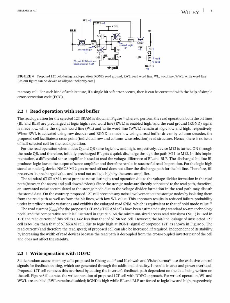
FIGURE 4 Proposed 12T cell during read operation. RGND, read ground; RWL, read word line; WL, word line; WWL, write word line[Colour figure can be viewed at wileyonlinelibrary.com]
memory cell. For such kind of architecture, if a single bit soft error occurs, then it can be corrected with the help of simpleerror correction code (ECC).
2.2 Read operation with read bufferThe read operation for the selected 12T SRAM is shown in Figure 4 where to perform the read operation, both the bit lines(BL and BLB) are precharged at logic high; read word line (RWL) is enabled high; and the read ground (RGND) signalis made low, while the signals word line (WL) and write word line (WWL) remain at logic low and high, respectively.When RWL is activated using row decoder and RGND is made low using a read buffer driven by column decoder, theproposed cell facilitates a cross point (individual row and column-wise selection) read structure. Hence, there is no issueof half-selected cell for the read operation.
For the read operation when nodes Q and QB store logic low and high, respectively, device M12 is turned ON throughthe node QB, and therefore, initially precharged BL gets a quick discharge through the path M11 to M12. In this imple-mentation, a differential sense amplifier is used to read the voltage difference of BL and BLB. The discharged bit line BLproduces logic low at the output of sense amplifier and therefore results in successful read 0 operation. For the logic highstored at node Q, device NMOS M12 gets turned off and does not allow the discharge path for the bit line. Therefore, BLpreserves its precharged value and is read out as logic high by the sense amplifier.
The standard 6T SRAM is most prone to noise during its read operation due to the voltage divider formation in the readpath (between the access and pull down devices). Since the storage nodes are directly connected to the read path, therefore,an unwanted noise accumulated at the storage node due to the voltage divider formation in the read path may disturbthe stored data. On the contrary, proposed 12T cell prevents any noise involvement at the storage nodes by isolating themfrom the read path as well as from the bit lines, with low WL value. This approach results in reduced failure probabilityunder interdie/intradie variations and exhibits the enlarged read SNM, which is equivalent to that of hold mode value.20
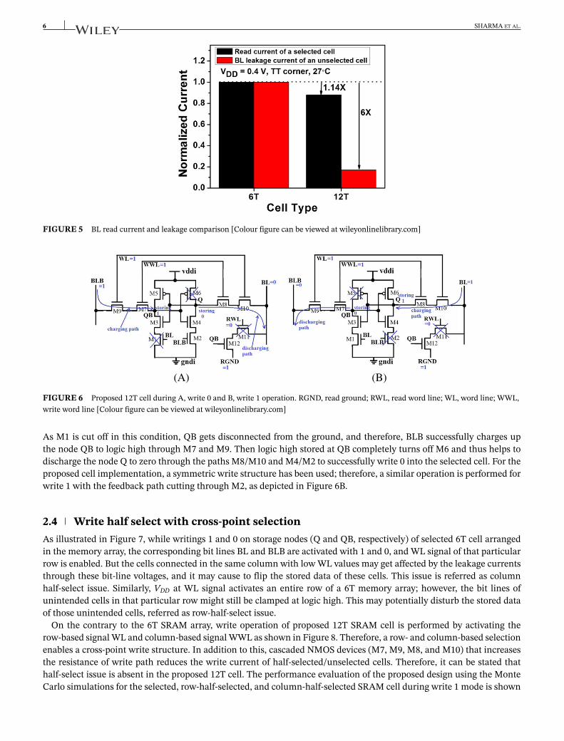
The read current (IRead) for the proposed 12T and 6T SRAM cells have been estimated using standard 65-nm technologynode, and the comparative result is illustrated in Figure 5. As the minimum-sized access read transistor (M11) is used in12T, the read current of this cell is 1.14× less than that of 6T SRAM cell. However, the bit-line leakage of unselected 12Tcell is 6× less than that of 6T SRAM cell, due to logic high at RGND signal of proposed 12T, as shown in Figure 5. Theread current (and therefore the read speed) of proposed cell can also be increased, if required, independent of its stabilityby increasing the width of read devices because the read path is decoupled from the cross-coupled inverter pair of the celland does not affect the stability.
2.3 Write operation with DDFCStatic random access memory cells proposed in Chang et al10 and Kushwah and Vishvakarma11 use the exclusive controlsignals for feedback cutting, which are generated through the additional circuitry. It results in area and power overhead.Proposed 12T cell removes this overhead by cutting the inverter's feedback path dependent on the data being written onthe cell. Figure 6 illustrates the write operation of proposed 12T cell with DDFC approach. For write 0 operation, WL andWWL are enabled; RWL remains disabled; RGND is high while BL and BLB are forced to logic low and high, respectively.
6 SHARMA ET AL.
FIGURE 5 BL read current and leakage comparison [Colour figure can be viewed at wileyonlinelibrary.com]
(A) (B)
FIGURE 6 Proposed 12T cell during A, write 0 and B, write 1 operation. RGND, read ground; RWL, read word line; WL, word line; WWL,write word line [Colour figure can be viewed at wileyonlinelibrary.com]
As M1 is cut off in this condition, QB gets disconnected from the ground, and therefore, BLB successfully charges upthe node QB to logic high through M7 and M9. Then logic high stored at QB completely turns off M6 and thus helps todischarge the node Q to zero through the paths M8/M10 and M4/M2 to successfully write 0 into the selected cell. For theproposed cell implementation, a symmetric write structure has been used; therefore, a similar operation is performed forwrite 1 with the feedback path cutting through M2, as depicted in Figure 6B.
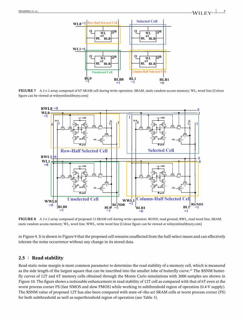
2.4 Write half select with cross-point selectionAs illustrated in Figure 7, while writings 1 and 0 on storage nodes (Q and QB, respectively) of selected 6T cell arrangedin the memory array, the corresponding bit lines BL and BLB are activated with 1 and 0, and WL signal of that particularrow is enabled. But the cells connected in the same column with low WL values may get affected by the leakage currentsthrough these bit-line voltages, and it may cause to flip the stored data of these cells. This issue is referred as columnhalf-select issue. Similarly, VDD at WL signal activates an entire row of a 6T memory array; however, the bit lines ofunintended cells in that particular row might still be clamped at logic high. This may potentially disturb the stored dataof those unintended cells, referred as row-half-select issue.
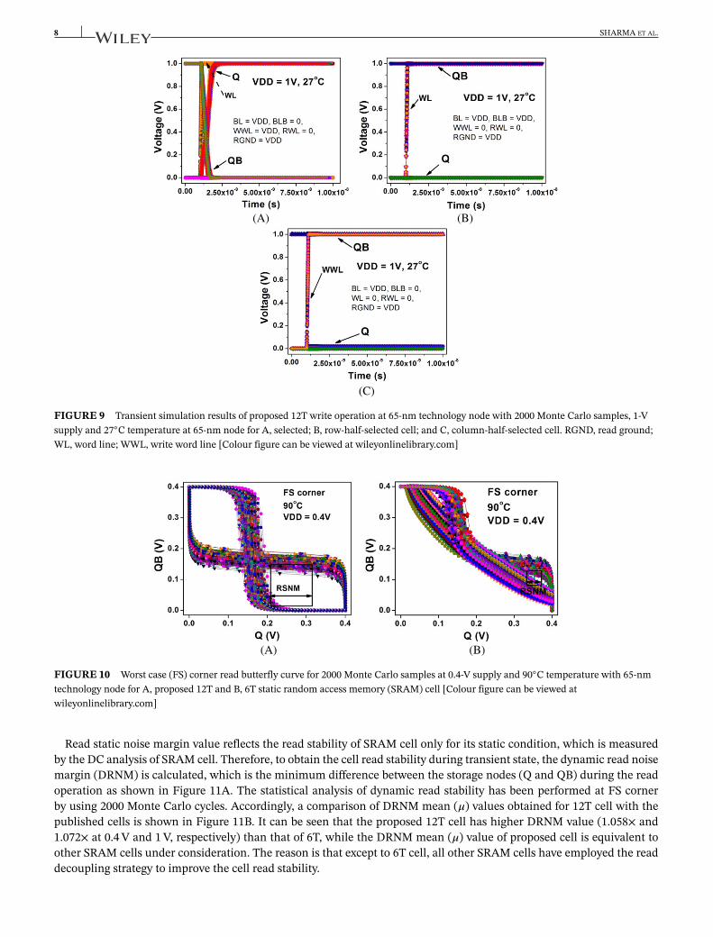
On the contrary to the 6T SRAM array, write operation of proposed 12T SRAM cell is performed by activating therow-based signal WL and column-based signal WWL as shown in Figure 8. Therefore, a row- and column-based selectionenables a cross-point write structure. In addition to this, cascaded NMOS devices (M7, M9, M8, and M10) that increasesthe resistance of write path reduces the write current of half-selected/unselected cells. Therefore, it can be stated thathalf-select issue is absent in the proposed 12T cell. The performance evaluation of the proposed design using the MonteCarlo simulations for the selected, row-half-selected, and column-half-selected SRAM cell during write 1 mode is shown
SHARMA ET AL. 7
FIGURE 7 A 2× 2 array composed of 6T SRAM cell during write operation. SRAM, static random access memory; WL, word line [Colourfigure can be viewed at wileyonlinelibrary.com]
FIGURE 8 A 2× 2 array composed of proposed 12 SRAM cell during write operation. RGND, read ground; RWL, read word line; SRAM,static random access memory; WL, word line; WWL, write word line [Colour figure can be viewed at wileyonlinelibrary.com]
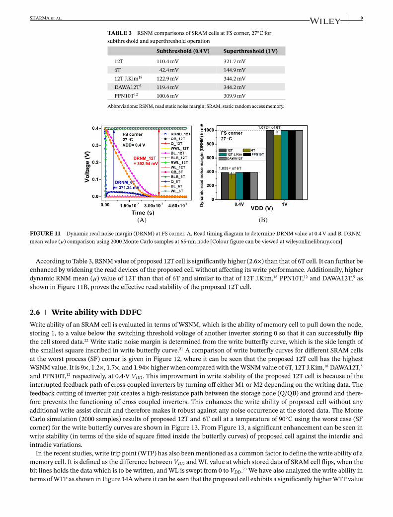
in Figure 9. It is shown in Figure 9 that the proposed cell remains unaffected from the half-select issues and can effectivelytolerate the noise occurrence without any change in its stored data.
2.5 Read stabilityRead static noise margin is most common parameter to determine the read stability of a memory cell, which is measuredas the side length of the largest square that can be inscribed into the smaller lobe of butterfly curve.21 The RSNM butter-fly curves of 12T and 6T memory cells obtained through the Monte Carlo simulations with 2000 samples are shown inFigure 10. The figure shows a noticeable enhancement in read stability of 12T cell as compared with that of 6T even at theworst process corner FS (fast NMOS and slow PMOS) while working in subthreshold region of operation (0.4-V supply).The RSNM value of proposed 12T has also been compared with state-of–the-art SRAM cells at worst process corner (FS)for both subthreshold as well as superthreshold region of operation (see Table 3).
8 SHARMA ET AL.
(B)(A)
(C)
FIGURE 9 Transient simulation results of proposed 12T write operation at 65-nm technology node with 2000 Monte Carlo samples, 1-Vsupply and 27◦C temperature at 65-nm node for A, selected; B, row-half-selected cell; and C, column-half-selected cell. RGND, read ground;WL, word line; WWL, write word line [Colour figure can be viewed at wileyonlinelibrary.com]
(A) (B)
FIGURE 10 Worst case (FS) corner read butterfly curve for 2000 Monte Carlo samples at 0.4-V supply and 90◦C temperature with 65-nmtechnology node for A, proposed 12T and B, 6T static random access memory (SRAM) cell [Colour figure can be viewed atwileyonlinelibrary.com]
Read static noise margin value reflects the read stability of SRAM cell only for its static condition, which is measuredby the DC analysis of SRAM cell. Therefore, to obtain the cell read stability during transient state, the dynamic read noisemargin (DRNM) is calculated, which is the minimum difference between the storage nodes (Q and QB) during the readoperation as shown in Figure 11A. The statistical analysis of dynamic read stability has been performed at FS cornerby using 2000 Monte Carlo cycles. Accordingly, a comparison of DRNM mean (𝜇) values obtained for 12T cell with thepublished cells is shown in Figure 11B. It can be seen that the proposed 12T cell has higher DRNM value (1.058× and1.072× at 0.4 V and 1 V, respectively) than that of 6T, while the DRNM mean (𝜇) value of proposed cell is equivalent toother SRAM cells under consideration. The reason is that except to 6T cell, all other SRAM cells have employed the readdecoupling strategy to improve the cell read stability.
SHARMA ET AL. 9
TABLE 3 RSNM comparisons of SRAM cells at FS corner, 27◦C forsubthreshold and superthreshold operation
Subthreshold (0.4 V) Superthreshold (1 V)
12T 110.4 mV 321.7 mV6T 42.4 mV 144.9 mV12T J.Kim18 122.9 mV 344.2 mVDAWA12T5 119.4 mV 344.2 mVPPN10T12 100.6 mV 309.9 mV
Abbreviations: RSNM, read static noise margin; SRAM, static random access memory.
(A) (B)
FIGURE 11 Dynamic read noise margin (DRNM) at FS corner. A, Read timing diagram to determine DRNM value at 0.4 V and B, DRNMmean value (𝜇) comparison using 2000 Monte Carlo samples at 65-nm node [Colour figure can be viewed at wileyonlinelibrary.com]
According to Table 3, RSNM value of proposed 12T cell is significantly higher (2.6×) than that of 6T cell. It can further beenhanced by widening the read devices of the proposed cell without affecting its write performance. Additionally, higherdynamic RNM mean (𝜇) value of 12T than that of 6T and similar to that of 12T J.Kim,18 PPN10T,12 and DAWA12T,5 asshown in Figure 11B, proves the effective read stability of the proposed 12T cell.
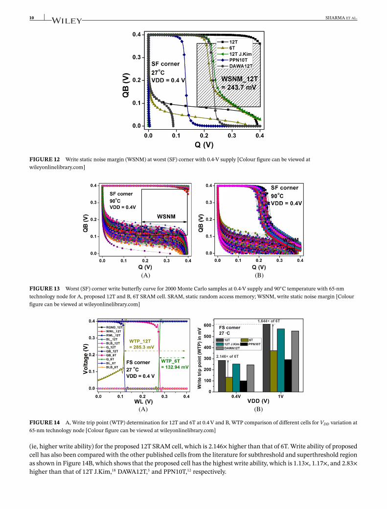
2.6 Write ability with DDFCWrite ability of an SRAM cell is evaluated in terms of WSNM, which is the ability of memory cell to pull down the node,storing 1, to a value below the switching threshold voltage of another inverter storing 0 so that it can successfully flipthe cell stored data.22 Write static noise margin is determined from the write butterfly curve, which is the side length ofthe smallest square inscribed in write butterfly curve.21 A comparison of write butterfly curves for different SRAM cellsat the worst process (SF) corner is given in Figure 12, where it can be seen that the proposed 12T cell has the highestWSNM value. It is 9×, 1.2×, 1.7×, and 1.94× higher when compared with the WSNM value of 6T, 12T J.Kim,18 DAWA12T,5
and PPN10T,12 respectively, at 0.4-V VDD. This improvement in write stability of the proposed 12T cell is because of theinterrupted feedback path of cross-coupled inverters by turning off either M1 or M2 depending on the writing data. Thefeedback cutting of inverter pair creates a high-resistance path between the storage node (Q/QB) and ground and there-fore prevents the functioning of cross coupled inverters. This enhances the write ability of proposed cell without anyadditional write assist circuit and therefore makes it robust against any noise occurrence at the stored data. The MonteCarlo simulation (2000 samples) results of proposed 12T and 6T cell at a temperature of 90◦C using the worst case (SFcorner) for the write butterfly curves are shown in Figure 13. From Figure 13, a significant enhancement can be seen inwrite stability (in terms of the side of square fitted inside the butterfly curves) of proposed cell against the interdie andintradie variations.
In the recent studies, write trip point (WTP) has also been mentioned as a common factor to define the write ability of amemory cell. It is defined as the difference between VDD and WL value at which stored data of SRAM cell flips, when thebit lines holds the data which is to be written, and WL is swept from 0 to VDD.23 We have also analyzed the write ability interms of WTP as shown in Figure 14A where it can be seen that the proposed cell exhibits a significantly higher WTP value
10 SHARMA ET AL.
FIGURE 12 Write static noise margin (WSNM) at worst (SF) corner with 0.4-V supply [Colour figure can be viewed atwileyonlinelibrary.com]
(A) (B)
FIGURE 13 Worst (SF) corner write butterfly curve for 2000 Monte Carlo samples at 0.4-V supply and 90◦C temperature with 65-nmtechnology node for A, proposed 12T and B, 6T SRAM cell. SRAM, static random access memory; WSNM, write static noise margin [Colourfigure can be viewed at wileyonlinelibrary.com]
(A) (B)
FIGURE 14 A, Write trip point (WTP) determination for 12T and 6T at 0.4 V and B, WTP comparison of different cells for VDD variation at65-nm technology node [Colour figure can be viewed at wileyonlinelibrary.com]
(ie, higher write ability) for the proposed 12T SRAM cell, which is 2.146× higher than that of 6T. Write ability of proposedcell has also been compared with the other published cells from the literature for subthreshold and superthreshold regionas shown in Figure 14B, which shows that the proposed cell has the highest write ability, which is 1.13×, 1.17×, and 2.83×higher than that of 12T J.Kim,18 DAWA12T,5 and PPN10T,12 respectively.
SHARMA ET AL. 11
(A) (B)
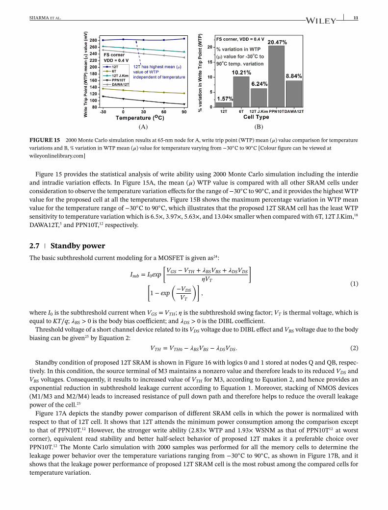
FIGURE 15 2000 Monte Carlo simulation results at 65-nm node for A, write trip point (WTP) mean (𝜇) value comparison for temperaturevariations and B, % variation in WTP mean (𝜇) value for temperature varying from −30◦C to 90◦C [Colour figure can be viewed atwileyonlinelibrary.com]
Figure 15 provides the statistical analysis of write ability using 2000 Monte Carlo simulation including the interdieand intradie variation effects. In Figure 15A, the mean (𝜇) WTP value is compared with all other SRAM cells underconsideration to observe the temperature variation effects for the range of −30◦C to 90◦C, and it provides the highest WTPvalue for the proposed cell at all the temperatures. Figure 15B shows the maximum percentage variation in WTP meanvalue for the temperature range of −30◦C to 90◦C, which illustrates that the proposed 12T SRAM cell has the least WTPsensitivity to temperature variation which is 6.5×, 3.97×, 5.63×, and 13.04× smaller when compared with 6T, 12T J.Kim,18
DAWA12T,5 and PPN10T,12 respectively.
2.7 Standby powerThe basic subthreshold current modeling for a MOSFET is given as24:
Isub = I0exp[
VGS − VTH + 𝜆BSVBS + 𝜆DSVDS
𝜂VT
][
1 − exp(−VDS
VT
)],
(1)
where I0 is the subthreshold current when VGS = VTH; 𝜂 is the subthreshold swing factor; VT is thermal voltage, which isequal to KT∕q; 𝜆BS > 0 is the body bias coefficient; and 𝜆DS > 0 is the DIBL coefficient.
Threshold voltage of a short channel device related to its VDS voltage due to DIBL effect and VBS voltage due to the bodybiasing can be given25 by Equation 2:
VTH = VTH0 − 𝜆BSVBS − 𝜆DSVDS. (2)
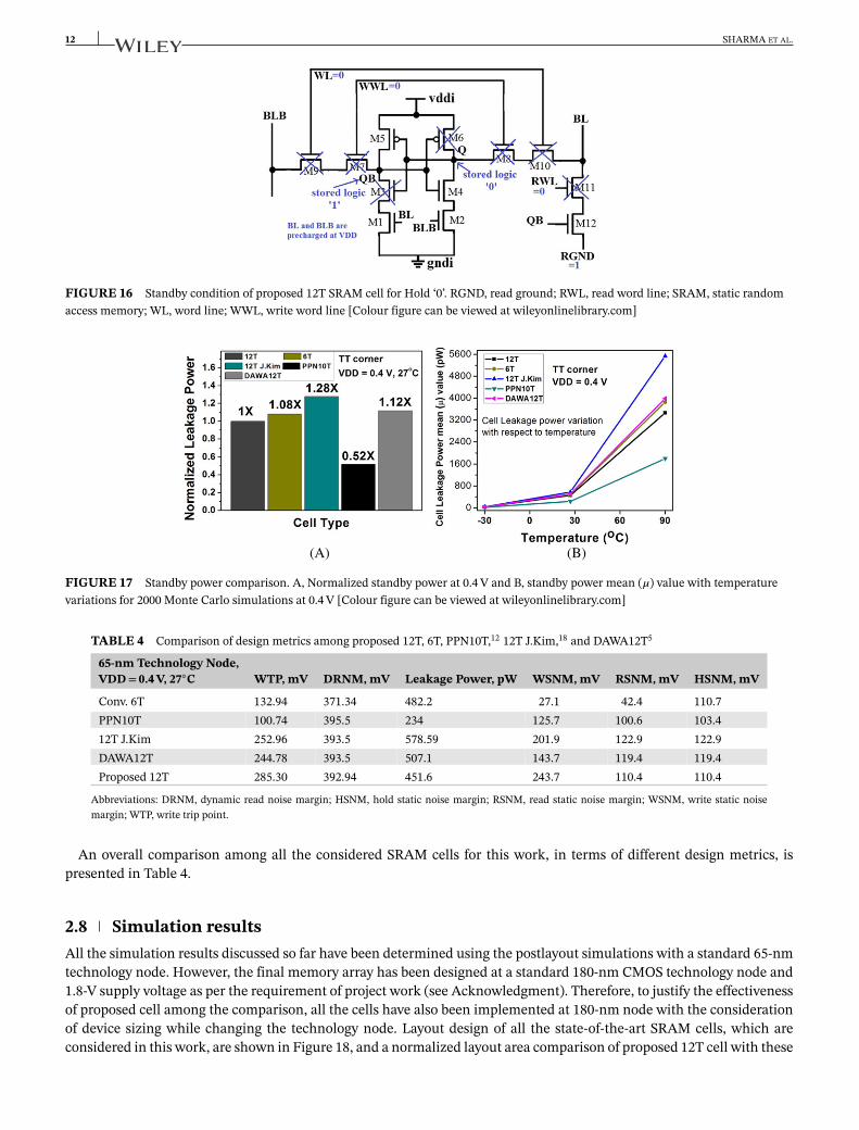
Standby condition of proposed 12T SRAM is shown in Figure 16 with logics 0 and 1 stored at nodes Q and QB, respec-tively. In this condition, the source terminal of M3 maintains a nonzero value and therefore leads to its reduced VDS andVBS voltages. Consequently, it results to increased value of VTH for M3, according to Equation 2, and hence provides anexponential reduction in subthreshold leakage current according to Equation 1. Moreover, stacking of NMOS devices(M1/M3 and M2/M4) leads to increased resistance of pull down path and therefore helps to reduce the overall leakagepower of the cell.23
Figure 17A depicts the standby power comparison of different SRAM cells in which the power is normalized withrespect to that of 12T cell. It shows that 12T attends the minimum power consumption among the comparison exceptto that of PPN10T.12 However, the stronger write ability (2.83× WTP and 1.93× WSNM as that of PPN10T12 at worstcorner), equivalent read stability and better half-select behavior of proposed 12T makes it a preferable choice overPPN10T.12 The Monte Carlo simulation with 2000 samples was performed for all the memory cells to determine theleakage power behavior over the temperature variations ranging from −30◦C to 90◦C, as shown in Figure 17B, and itshows that the leakage power performance of proposed 12T SRAM cell is the most robust among the compared cells fortemperature variation.
12 SHARMA ET AL.
FIGURE 16 Standby condition of proposed 12T SRAM cell for Hold ‘0’. RGND, read ground; RWL, read word line; SRAM, static randomaccess memory; WL, word line; WWL, write word line [Colour figure can be viewed at wileyonlinelibrary.com]
(A) (B)
FIGURE 17 Standby power comparison. A, Normalized standby power at 0.4 V and B, standby power mean (𝜇) value with temperaturevariations for 2000 Monte Carlo simulations at 0.4 V [Colour figure can be viewed at wileyonlinelibrary.com]
TABLE 4 Comparison of design metrics among proposed 12T, 6T, PPN10T,12 12T J.Kim,18 and DAWA12T5
65-nm Technology Node,VDD= 0.4 V, 27◦C WTP, mV DRNM, mV Leakage Power, pW WSNM, mV RSNM, mV HSNM, mV
Conv. 6T 132.94 371.34 482.2 27.1 42.4 110.7PPN10T 100.74 395.5 234 125.7 100.6 103.412T J.Kim 252.96 393.5 578.59 201.9 122.9 122.9DAWA12T 244.78 393.5 507.1 143.7 119.4 119.4Proposed 12T 285.30 392.94 451.6 243.7 110.4 110.4
Abbreviations: DRNM, dynamic read noise margin; HSNM, hold static noise margin; RSNM, read static noise margin; WSNM, write static noisemargin; WTP, write trip point.
An overall comparison among all the considered SRAM cells for this work, in terms of different design metrics, ispresented in Table 4.
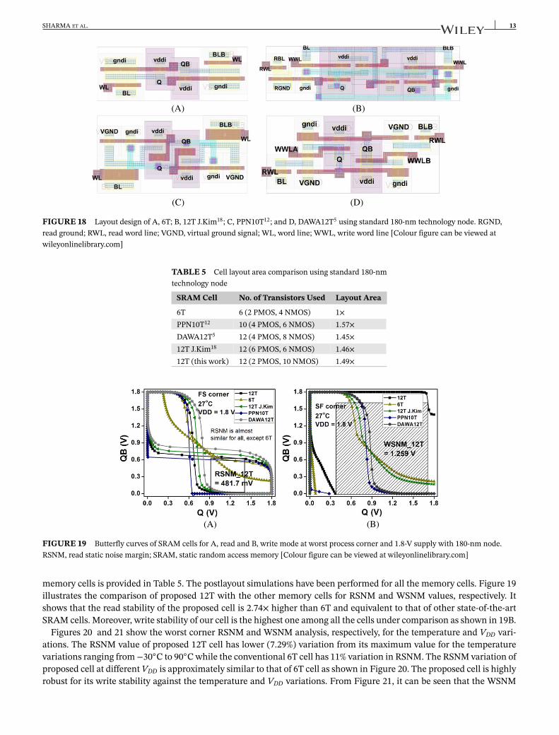
2.8 Simulation resultsAll the simulation results discussed so far have been determined using the postlayout simulations with a standard 65-nmtechnology node. However, the final memory array has been designed at a standard 180-nm CMOS technology node and1.8-V supply voltage as per the requirement of project work (see Acknowledgment). Therefore, to justify the effectivenessof proposed cell among the comparison, all the cells have also been implemented at 180-nm node with the considerationof device sizing while changing the technology node. Layout design of all the state-of-the-art SRAM cells, which areconsidered in this work, are shown in Figure 18, and a normalized layout area comparison of proposed 12T cell with these
SHARMA ET AL. 13
(A) (B)
(C) (D)
FIGURE 18 Layout design of A, 6T; B, 12T J.Kim18; C, PPN10T12; and D, DAWA12T5 using standard 180-nm technology node. RGND,read ground; RWL, read word line; VGND, virtual ground signal; WL, word line; WWL, write word line [Colour figure can be viewed atwileyonlinelibrary.com]
TABLE 5 Cell layout area comparison using standard 180-nmtechnology node
SRAM Cell No. of Transistors Used Layout Area
6T 6 (2 PMOS, 4 NMOS) 1×PPN10T12 10 (4 PMOS, 6 NMOS) 1.57×DAWA12T5 12 (4 PMOS, 8 NMOS) 1.45×12T J.Kim18 12 (6 PMOS, 6 NMOS) 1.46×12T (this work) 12 (2 PMOS, 10 NMOS) 1.49×
(A) (B)
FIGURE 19 Butterfly curves of SRAM cells for A, read and B, write mode at worst process corner and 1.8-V supply with 180-nm node.RSNM, read static noise margin; SRAM, static random access memory [Colour figure can be viewed at wileyonlinelibrary.com]
memory cells is provided in Table 5. The postlayout simulations have been performed for all the memory cells. Figure 19illustrates the comparison of proposed 12T with the other memory cells for RSNM and WSNM values, respectively. Itshows that the read stability of the proposed cell is 2.74× higher than 6T and equivalent to that of other state-of-the-artSRAM cells. Moreover, write stability of our cell is the highest one among all the cells under comparison as shown in 19B.
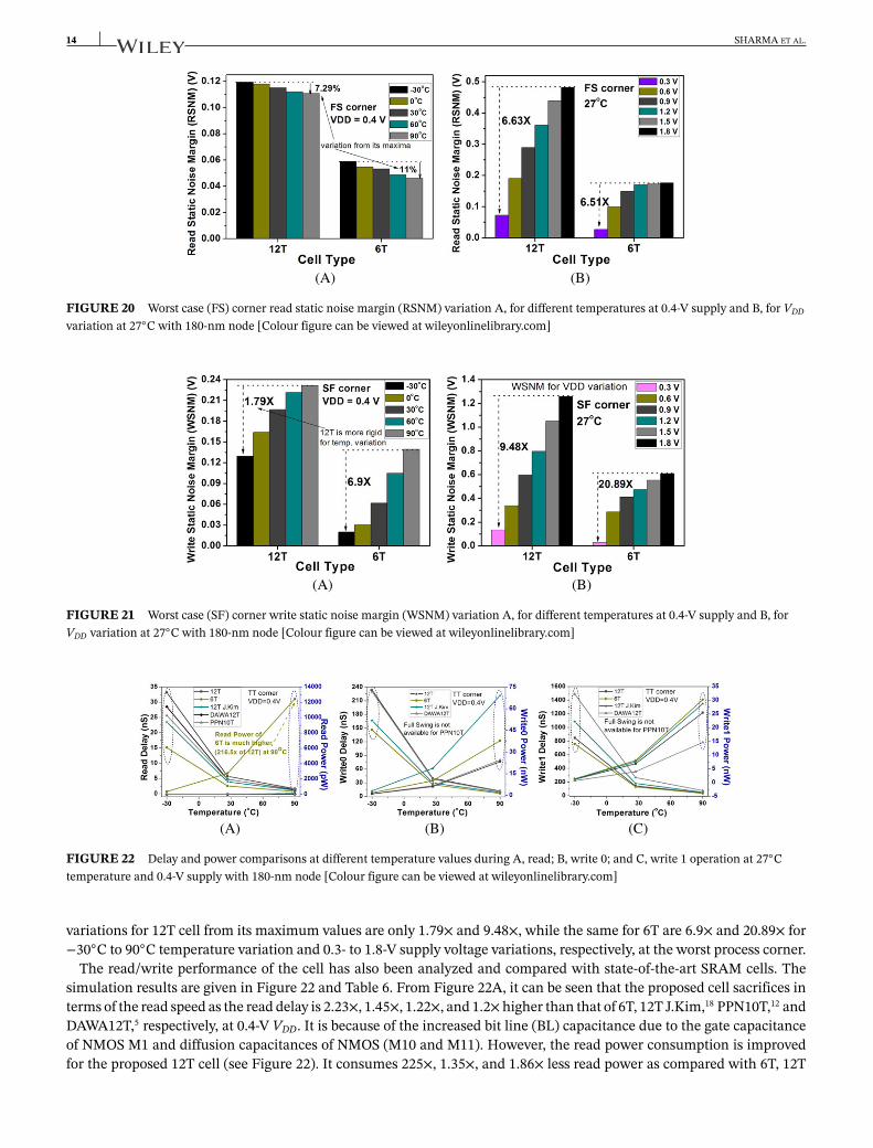
Figures 20 and 21 show the worst corner RSNM and WSNM analysis, respectively, for the temperature and VDD vari-ations. The RSNM value of proposed 12T cell has lower (7.29%) variation from its maximum value for the temperaturevariations ranging from −30◦C to 90◦C while the conventional 6T cell has 11% variation in RSNM. The RSNM variation ofproposed cell at different VDD is approximately similar to that of 6T cell as shown in Figure 20. The proposed cell is highlyrobust for its write stability against the temperature and VDD variations. From Figure 21, it can be seen that the WSNM
14 SHARMA ET AL.
(A) (B)
FIGURE 20 Worst case (FS) corner read static noise margin (RSNM) variation A, for different temperatures at 0.4-V supply and B, for VDD
variation at 27◦C with 180-nm node [Colour figure can be viewed at wileyonlinelibrary.com]
(A) (B)
FIGURE 21 Worst case (SF) corner write static noise margin (WSNM) variation A, for different temperatures at 0.4-V supply and B, forVDD variation at 27◦C with 180-nm node [Colour figure can be viewed at wileyonlinelibrary.com]
(A) (B) (C)
FIGURE 22 Delay and power comparisons at different temperature values during A, read; B, write 0; and C, write 1 operation at 27◦Ctemperature and 0.4-V supply with 180-nm node [Colour figure can be viewed at wileyonlinelibrary.com]
variations for 12T cell from its maximum values are only 1.79× and 9.48×, while the same for 6T are 6.9× and 20.89× for−30◦C to 90◦C temperature variation and 0.3- to 1.8-V supply voltage variations, respectively, at the worst process corner.
The read/write performance of the cell has also been analyzed and compared with state-of-the-art SRAM cells. Thesimulation results are given in Figure 22 and Table 6. From Figure 22A, it can be seen that the proposed cell sacrifices interms of the read speed as the read delay is 2.23×, 1.45×, 1.22×, and 1.2×higher than that of 6T, 12T J.Kim,18 PPN10T,12 andDAWA12T,5 respectively, at 0.4-V VDD. It is because of the increased bit line (BL) capacitance due to the gate capacitanceof NMOS M1 and diffusion capacitances of NMOS (M10 and M11). However, the read power consumption is improvedfor the proposed 12T cell (see Figure 22). It consumes 225×, 1.35×, and 1.86× less read power as compared with 6T, 12T
SHARMA ET AL. 15
TABLE 6 Power delay product (PDP) comparison during read, write 0, and write 1 operation
180-nm technology node,VDD= 0.4 V, 27◦C 12T 6T 12T J.Kim18 PPN10T12 DAWA12T5
Write 0 PDP (10−18) 242.946 263.934 558.154 Full swing is not available 254.37Write 1 PDP (10−18) 981.274 1047.08 1378.79 Full swing is not available 1057.34Read PDP (10−21) 69.34 6992.62 64.52 106.08 61.41
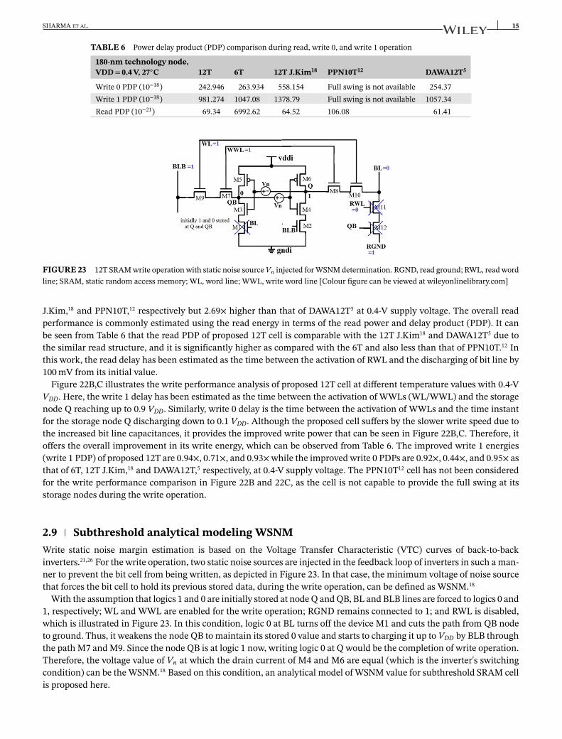
FIGURE 23 12T SRAM write operation with static noise source Vn injected for WSNM determination. RGND, read ground; RWL, read wordline; SRAM, static random access memory; WL, word line; WWL, write word line [Colour figure can be viewed at wileyonlinelibrary.com]
J.Kim,18 and PPN10T,12 respectively but 2.69× higher than that of DAWA12T5 at 0.4-V supply voltage. The overall readperformance is commonly estimated using the read energy in terms of the read power and delay product (PDP). It canbe seen from Table 6 that the read PDP of proposed 12T cell is comparable with the 12T J.Kim18 and DAWA12T5 due tothe similar read structure, and it is significantly higher as compared with the 6T and also less than that of PPN10T.12 Inthis work, the read delay has been estimated as the time between the activation of RWL and the discharging of bit line by100 mV from its initial value.
Figure 22B,C illustrates the write performance analysis of proposed 12T cell at different temperature values with 0.4-VVDD. Here, the write 1 delay has been estimated as the time between the activation of WWLs (WL/WWL) and the storagenode Q reaching up to 0.9 VDD. Similarly, write 0 delay is the time between the activation of WWLs and the time instantfor the storage node Q discharging down to 0.1 VDD. Although the proposed cell suffers by the slower write speed due tothe increased bit line capacitances, it provides the improved write power that can be seen in Figure 22B,C. Therefore, itoffers the overall improvement in its write energy, which can be observed from Table 6. The improved write 1 energies(write 1 PDP) of proposed 12T are 0.94×, 0.71×, and 0.93× while the improved write 0 PDPs are 0.92×, 0.44×, and 0.95× asthat of 6T, 12T J.Kim,18 and DAWA12T,5 respectively, at 0.4-V supply voltage. The PPN10T12 cell has not been consideredfor the write performance comparison in Figure 22B and 22C, as the cell is not capable to provide the full swing at itsstorage nodes during the write operation.
2.9 Subthreshold analytical modeling WSNMWrite static noise margin estimation is based on the Voltage Transfer Characteristic (VTC) curves of back-to-backinverters.21,26 For the write operation, two static noise sources are injected in the feedback loop of inverters in such a man-ner to prevent the bit cell from being written, as depicted in Figure 23. In that case, the minimum voltage of noise sourcethat forces the bit cell to hold its previous stored data, during the write operation, can be defined as WSNM.18
With the assumption that logics 1 and 0 are initially stored at node Q and QB, BL and BLB lines are forced to logics 0 and1, respectively; WL and WWL are enabled for the write operation; RGND remains connected to 1; and RWL is disabled,which is illustrated in Figure 23. In this condition, logic 0 at BL turns off the device M1 and cuts the path from QB nodeto ground. Thus, it weakens the node QB to maintain its stored 0 value and starts to charging it up to VDD by BLB throughthe path M7 and M9. Since the node QB is at logic 1 now, writing logic 0 at Q would be the completion of write operation.Therefore, the voltage value of Vn at which the drain current of M4 and M6 are equal (which is the inverter's switchingcondition) can be the WSNM.18 Based on this condition, an analytical model of WSNM value for subthreshold SRAM cellis proposed here.
16 SHARMA ET AL.
By equating the subthreshold drain current of M4 and M6 to estimate the WSNM value,
ISDM6 = IDSM4 . (3)
After substituting the values of ISDM6 and IDSM4 and then solving the equation (the detailed derivation is given in theAppendix A), finally, we get the WSNM analytical model as follows:
WSNMsub = Vn = 12
[VDD − VTHn + VTHp
+𝜂VTloge
[𝜇n
𝜇p
(WL)M4
(WL)M6
]].
(4)
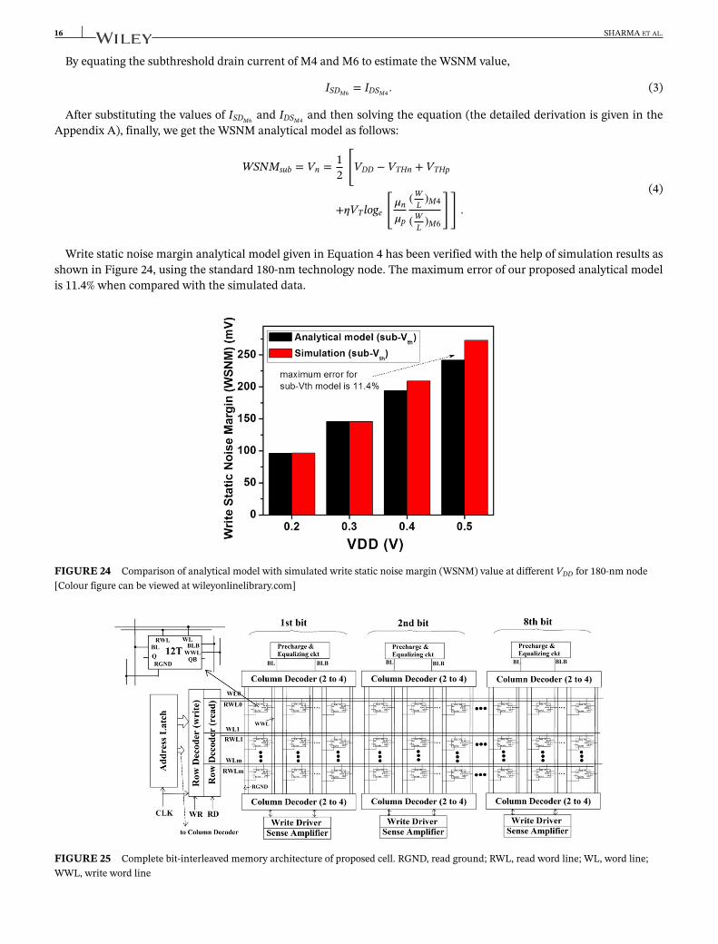
Write static noise margin analytical model given in Equation 4 has been verified with the help of simulation results asshown in Figure 24, using the standard 180-nm technology node. The maximum error of our proposed analytical modelis 11.4% when compared with the simulated data.
FIGURE 24 Comparison of analytical model with simulated write static noise margin (WSNM) value at different VDD for 180-nm node[Colour figure can be viewed at wileyonlinelibrary.com]
FIGURE 25 Complete bit-interleaved memory architecture of proposed cell. RGND, read ground; RWL, read word line; WL, word line;WWL, write word line
SHARMA ET AL. 17
(A) (B)
FIGURE 26 A, Custom layout design of 256-bits memory array with its independent memory controller and B, memory placed in the ring.SRAM, static random access memory [Colour figure can be viewed at wileyonlinelibrary.com]
FIGURE 27 Transient simulation results of memory array
3 MEMORY ARRAY DESIGN
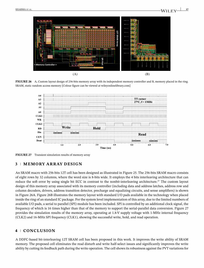
An SRAM macro with 256-bits 12T cell has been designed as illustrated in Figure 25. The 256-bits SRAM macro consistsof eight rows by 32 columns, where the word size is 8-bits wide. It employs the 4 bits interleaving architecture that canreduce the soft error by using single bit ECC in contrast to the nonbit-interleaving architecture.27 The custom layoutdesign of this memory array associated with its memory controller (including data and address latches, address row andcolumn decoders, drivers, address transition detector, precharge and equalizing circuits, and sense amplifiers) is shownin Figure 26A. Figure 26B illustrates the memory layout with standard I/O pads available in the technology when placedinside the ring of an standard IC package. For the system level implementation of this array, due to the limited numbers ofavailable I/O pads, a serial to parallel (SPI) module has been included. SPI is controlled by an additional clock signal, thefrequency of which is 16 times higher than that of the memory to support the serial-parallel data conversion. Figure 27provides the simulation results of the memory array, operating at 1.8-V supply voltage with 1-MHz internal frequency(CLK2) and 16-MHz SPI frequency (CLK1), showing the successful write, hold, and read operation.
4 CONCLUSION
A DDFC-based bit-interleaving 12T SRAM cell has been proposed in this work. It improves the write ability of SRAMmemory. The proposed cell eliminates the read disturb and write half-select issues and significantly improves the writeability by cutting its feedback path during the write operation. The cell shows its robustness against the PVT variations for
18 SHARMA ET AL.
both subthreshold and superthreshold operating region, which has been verified by using the Monte Carlo simulations.The leakage power and read stability of proposed cell is also improved as compared with that of standard 6T cell. Moreover,an analytical model of WSNM for subthreshold 12T SRAM is proposed, and it fits within the maximum error of 11.4% at180-nm technology node. Furthermore, a 256-bits SRAM macro has been designed for 32-kHz operating frequency and1.8-V supply, considering all the factors required for its fabrication using a standard IC package. The simulated powerconsumption of the macro during its standby, read, and write mode at above specified VDD and frequency is 24.44, 28.62,and 35.09 nW, respectively. The above-mentioned characteristics make the proposed SRAM cell useful to be deployed asa part of memory in BSNs, on-chip computations, and movable IoT applications.
ACKNOWLEDGMENTS
The authors are thankful to Center for International Mobility (CIMO grant no Intia-1-2016-03) and Aalto University,Finland, for their financial support. Also, the authors are thankful to Special Manpower Development Program for Chipsto System Design (SMDP-C2SD) research project of Department of Electronics and Information Technology (DEITY)under Ministry of Communication and Information Technology, Government of India for providing the lab facilities.
ORCID
Santosh Vishvakarma http://orcid.org/0000-0003-4223-0077
REFERENCES1. Patel HN, Yahya FB, Calhoun BH. Optimizing SRAM bitcell reliability and energy for IoT applications. 17th International Symposium on
Quality Electronic Design (ISQED). Santa Clara, CA: IEEE; 2016:12-17.2. Chen Y-H, Krishna T, Emer JS, Sze V. Eyeriss: An energy-efficient reconfigurable accelerator for deep convolutional neural networks.
IEEE J Solid-State Circuits. 2017;52(1):127-138.3. Lane ND, Bhattacharya S, Georgiev P, Forlivesi C, Kawsar F. An early resource characterization of deep learning on wearables, smart-
phones and internet-of-things devices. Proceedings of the 2015 International Workshop on Internet of Things towards Applications. Seoul,South Korea: ACM; 2015:7-12.
4. Sharma V, Kumar S. Design of low-power CMOS cell structures using subthreshold conduction region. Int J Sci Eng Res. 2011:29.5. Chiu Y-W, Hu Y-H, Tu M-H, et al. 40 nm bit-interleaving 12T subthreshold SRAM with data-aware write-assist. IEEE Trans Circuits Syst
I: Regul Pap. 2014;61(9):2578-2585.6. Chang M-F, Chen M-P, Chen L-F, et al. A sub-0.3 V area-efficient L-shaped 7T SRAM with read bitline swing expansion schemes based on
boosted read-bitline, asymmetric-vth read-port, and offset cell VDD biasing techniques. IEEE J Solid-State Circuits. 2013;48(10):2558-2569.7. Raychowdhury A, Mukhopadhyay S, Roy K. A feasibility study of subthreshold SRAM across technology generations. Proceedings of IEEE
International Conference on Computer Design: VLSI in Computers and Processors (ICCD). San Jose, CA: IEEE; 2005:417-422.8. Verma N, Chandrakasan AP. A 256kb 65 nm 8T subthreshold SRAM employing sense-amplifier redundancy. IEEE J Solid-State Circuits.
2008;43(1):141-149.9. Kim T-H, Liu J, Keane J, Kim CH. A 0.2 V, 480kb subthreshold SRAM with 1 k cells per bitline for ultra-low-voltage computing. IEEE J
Solid-State Circuits. 2008;43(2):518-529.10. Chang M-F, Chang S-W, Chou P-W, Wu W-C. A 130 mV SRAM with expanded write and read margins for subthreshold applications.
IEEE J Solid-State Circuits. 2011;46(2):520-529.11. Kushwah C, Vishvakarma SK. A single-ended with dynamic feedback control 8T subthreshold SRAM cell. IEEE Trans Very Large Scale
Integr (VLSI) Syst. 2016;24(1):373-377.12. Lo C-H, Huang S-Y. PPN based 10T SRAM cell for low-leakage and resilient subthreshold operation. IEEE J Solid-State Circuits.
2011;46(3):695-704.13. Saeidi R, Sharifkhani M, Hajsadeghi K. A subthreshold symmetric SRAM cell with high read stability. IEEE Trans Circuits Syst II: Express
Briefs. 2014;61(1):26-30.14. Moghaddam M, Timarchi S, Moaiyeri MH, Eshghi M. An ultra-low-power 9T SRAM cell based on threshold voltage techniques. Circuits,
Syst, Signal Process. 2016;35(5):1437-1455.15. Wang B, Nguyen TQ, Do AT, Zhou J, Je M, Kim TT-H. Design of an ultra-low voltage 9T SRAM with equalized bitline leakage and
cam-assisted energy efficiency improvement. IEEE Trans Circuits Syst I: Regul Pap. 2015;62(2):441-448.16. Maroof N, Sohail M, Shin H. Charge-sharing read port with bitline pre-charging and sensing scheme for low-power SRAMs. Int J Circuit
Theory Appls. 2017;45(9):1231-1248.17. Jain S, Khare S, Yada S, et al. A 280mV-to-1.2 V wide-operating-range IA-32 processor in 32nm CMOS. IEEE International Solid-State
Circuits Conference Digest of Technical Papers (ISSCC). San Francisco, CA: IEEE; 2012:66-68.18. Kim J, Mazumder P. A robust 12T SRAM cell with improved write margin for ultra-low power applications in 40nm CMOS. Integr, VLSI
J. 2017;57:1-10.
SHARMA ET AL. 19
19. Pal S, Islam A. 9-T SRAM cell for reliable ultralow-power applications and solving multibit soft-error issue. IEEE Trans Device Mater Reliab.2016;16(2):172-182.
20. Kushwah C, Vishvakarma SK. Ultra-low power sub-threshold SRAM cell design to improve read static noise margin. Progress in VLSIDesign and Test. Berlin, Heidelberg: Springer; 2012:139-146.
21. Seevinck E, List FJ, Lohstroh J. Static-noise margin analysis of MOS SRAM cells. IEEE J solid-state circuits. 1987;22(5):748-754.22. Islam A, Hasan M. A technique to mitigate impact of process, voltage and temperature variations on design metrics of SRAM cell.
Microelectron Reliab. 2012;52(2):405-411.23. Ahmad S, Gupta MK, Alam N, Hasan M. Single-ended Schmitt-trigger-based robust low-power SRAM cell. IEEE Trans Very Large Scale
Integr (VLSI) Syst. 2016;24(8):2634-2642.24. Alioto M. Understanding DC behavior of subthreshold CMOS logic through closed-form analysis. IEEE Trans Circuits Syst I: Regul Pap.
2010;57(7):1597-1607.25. Narendra S, De V, Borkar S, Antoniadis DA, Chandrakasan AP. Full-chip subthreshold leakage power prediction and reduction techniques
for sub-0.18-/spl mu/m CMOS. IEEE J Solid-State Circuits. 2004;39(3):501-510.26. Bhavnagarwala A, Kosonocky S, Radens C, Stawiasz K, Mann R, Ye Q, Chin K. Fluctuation limits & scaling opportunities for CMOS SRAM
cells. IEDM Technical Digest. IEEE International Electron Devices Meeting, 2005. Washington, DC: IEEE; 2005:659-662.27. Baeg S, Wen S, Wong R. SRAM interleaving distance selection with a soft error failure model. IEEE Trans Nucl Sci. 2009;56(4):2111-2118.
How to cite this article: Sharma V, Vishvakarma S, Chouhan SS, Halonen K. A write-improved low-power 12TSRAM cell for wearable wireless sensor nodes. Int J Circ Theor Appl. 2018;1–20. https://doi.org/10.1002/cta.2555
APPENDIX A: DERIVATION OF SUBTHRESHOLD ANALYTICAL MODEL OF WSNM
The subthreshold drain current for a MOS device is given as4,24:
IDS = I0exp[
VGS − VTH
𝜂VT
] [1 − exp
(−VDS
VT
)],
where I0 = 𝜇Cox(W∕L)(𝜂 − 1)V 2T .
For this analysis, we have not considered the drain-induced barrier lowering (DIBL) and body bias effect for the sim-plicity. Moreover, since 1 >> exp
(−VDS
VT
), the term exp
(−VDS
VT
)can be ignored. Hence, the subthreshold drain current of
NMOS M4 and M6 in the proposed cell can be written as
IDSM4 = I0M4 exp[VGSM4 − VTHn
𝜂VT
],
ISDM6 = I0M6 exp[VSGM6 − VTHp
𝜂VT
].
By equating these current (IDSM4 and ISDM6 ) to determine the write static noise margin (WSNM) value we get
𝜇n
(WL
)M4
exp[VGSM4 − VTHn
𝜂VT
]=
𝜇p
(WL
)M6
exp[VSGM6 − VTHp
𝜂VT
].
(A1)
Figure 23 shows that BLB is connected to logic 1 for the write 0 operation, so M2 is on, and hence, the drain of M2 is 0.Therefore, VSGM6 = (VDD + Vn − VQB),VGSM4 = (VQB − Vn), and VQB = VDD. By putting these values in Equation A1 andthen solving, we get
𝜇n
(WL
)M4
exp[
VDD − Vn − VTHn
𝜂VT
]=
𝜇p
(WL
)M6
exp[Vn − VTHp
𝜂VT
].
(A2)
20 SHARMA ET AL.
Now using this Equation A2, the value of Vn that is equal to the WSNM value can be written as
WSNMsub = Vn = 12
[VDD − VTHn + VTHp
+ 𝜂VTloge
[𝜇n
𝜇p
(WL)M4
(WL)M6
]].
(A3)


![A robust 12T SRAM cell with improved write margin for ...web.eecs.umich.edu/~mazum/PAPERS-MAZUM/12T SRAM.pdfJun 27, 2015 · additional read transistors [11]. These additional devices](https://img.pdfslide.net/doc/110x75/6063a7081962ba71ca2d97b2/a-robust-12t-sram-cell-with-improved-write-margin-for-webeecsumichedumazumpapers-mazum12t.jpg)