Embed Size (px)
Citation preview
A zero charge-pump mismatch current tracking loop for reference spurreduction in PLLs
R.R. Manikandan n, Bharadwaj AmruturElectrical Communication Engineering Department, Indian Institute of Science, Bangalore 560012, India
a r t i c l e i n f o
Article history:Received 12 March 2014Received in revised form25 November 2014Accepted 10 March 2015
Keywords:Phase-locked loop (PLL)Charge-pumpCurrent mismatchReference spurDeterministic jitterStatic phase offset
a b s t r a c t
The charge-pump (CP) mismatch current is a dominant source of static phase error and reference spur inthe nano-meter CMOS PLL implementations due to its worsened channel length modulation effect. Thispaper presents a charge-pump (CP) mismatch current reduction technique utilizing an adaptive bodybias tuning of CP transistors and a zero CP mismatch current tracking PLL architecture for reference spursuppression. A chip prototype of the proposed circuit was implemented in 0:13 μm CMOS technology.The frequency synthesizer consumes 8.2 mA current from a 1.3 V supply voltage and achieves a phasenoise of �96.01 dBc/Hz @ 1 MHz offset from a 2.4 GHz RF carrier. The charge-pump measurementsusing the proposed calibration technique exhibited a mismatch current of less than 0.3 μA (0.55%) overthe VCO control voltage range of 0.3–1.0 V. The closed loop measurements show a minimized staticphase error of within 770 ps and a C9 dB reduction in reference spur level across the PLL outputfrequency range 2.4–2.5 GHz. The presented CP calibration technique compensates for the DC currentmismatch and the mismatch due to channel length modulation effect and therefore improves theperformance of CP-PLLs in nano-meter CMOS implementations.
& 2015 Elsevier Ltd. All rights reserved.
1. Introduction
Charge-pump phase locked loops (CP-PLLs) are widely used forfrequency synthesis, up conversion and down conversion of base-band signals in RF transceivers, and clock generation in digitalsystems [1]. Fig. 1 shows the block level description of a conven-tional CP-PLL. Implementation of CP-PLLs with high spectral purityand wide frequency tuning range in nano-scaled CMOS process isquite challenging [2–4]. Severely deteriorated channel lengthmodulation effect of nano-scaled CMOS process affects the match-ing between the charge-pump currents (Iup and Idn) and hencedegrades the performance of PLL by introducing a static phaseerror between the phase frequency detector (PFD) input signalsand reference spurs in the frequency spectrum of its output signal[5,6] as shown in Fig. 1.
The static phase error (Te) and the reference spur level (Pspur)(using narrow-band frequency modulation approximation) due toCP mismatch current can be expressed as [7,8]
Te ¼ Tpfd �ΔiIcp
ð1Þ
Pspur ðdBcÞ ¼ 20 logIcp � Rz � Kvco � Tpfdffiffiffi
2p �ΔI
Icp
� ��20 log
f reff pl
!ð2Þ
where Tpfd is the PFD reset delay,Δi is the CP mismatch current, Icpis the CP output current, Rz is the resistor value in the loop filter,Kvco is the VCO gain, fref is the reference frequency and fpl is thefrequency of pole in the loop filter given by ðCzþCpÞ=2π�Rz � Cz � Cp.
VCO architectures with low gain (Kvco) and wide frequencytuning range using switched capacitor banks [9] and dual pathcontrol techniques [10–13] are presented in the literature tominimize reference spurs. These techniques either require com-plex digital frequency calibration schemes [9] or suffer due tocoarse-path leakage current and charge injection issues [11].Randomization techniques in the charge distribution mechanismto the loop filter are proposed in [14–17] to minimize themagnitude of reference spurs. However, the performance of thesetechniques are limited due to the open loop generation of equaldelays and increased in-band phase noise performance.
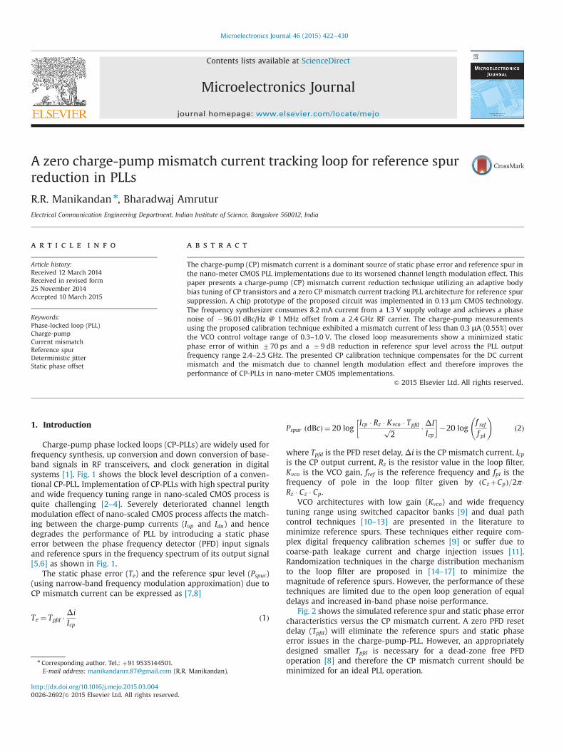
Fig. 2 shows the simulated reference spur and static phase errorcharacteristics versus the CP mismatch current. A zero PFD resetdelay (Tpfd) will eliminate the reference spurs and static phaseerror issues in the charge-pump-PLL. However, an appropriatelydesigned smaller Tpfd is necessary for a dead-zone free PFDoperation [8] and therefore the CP mismatch current should beminimized for an ideal PLL operation.
Contents lists available at ScienceDirect
journal homepage: www.elsevier.com/locate/mejo
Microelectronics Journal
http://dx.doi.org/10.1016/j.mejo.2015.03.0040026-2692/& 2015 Elsevier Ltd. All rights reserved.
n Corresponding author. Tel.: þ91 9535144501.E-mail address: [email protected] (R.R. Manikandan).
Microelectronics Journal 46 (2015) 422–430
Several CP mismatch current calibration schemes are presentedin the literature to minimize the pump current mismatch [18–26].A replica CP based mismatch current calibration scheme waspresented in [18]. However, Ref. [18] calibrates the CPs underdifferent control voltages and hence difficult to compensate for themismatch due to channel length modulation effect. A digitalmismatch current calibration approach was presented in[5,18,19]. However, the CP circuit implementations in thesereported works consume a larger current of 3nIcp, which is notsuitable for high output current (Icp) applications. Charge-pumparchitectures with negative feedback using high gain OPAMPs tominimize the mismatch current are presented in [22–26], but thenon-ideal effects of OPAMPs such as stability and offset voltagelimit the performance of CP.
Bulk-driven circuit techniques are highly useful in the design ofultra low voltage analog circuits [27–30] and to compensate forvariation effects (PVT, die-to-die and within-die), and to reducethe leakage power in digital circuits [31,32]. In this paper, wepresent a charge-pump mismatch current calibration techniqueutilizing an adaptive body bias tuning of its current sourcetransistors which provide a very fine resolution in the mismatchcurrent calibration and a zero CP mismatch current tracking PLLarchitecture to minimize the static phase error and referencespurs. The proposed technique compensates for the DC currentmismatch and the mismatch current due to channel length
modulation effect and hence improves the performance of CP-PLLs in the nano-scaled CMOS process implementations.
This paper is organized as follows. Section 2 describes theproposed CP mismatch current calibration scheme. The zero CPmismatch current tracking loop operation and its measured resultsare presented in Sections 3 and 4, respectively. Finally, theconclusions are given in Section 5.
2. Charge-pump mismatch current calibration technique
The current steering charge-pump circuit used in the PLL isshown in Fig. 3a. M7 and M3 are the up and down current sourcetransistors in the charge-pump, respectively, and their saturationcurrents can be expressed as
Iup ¼12μpCox;p
WL
� �pðVgs;p�VT ;pÞ2ð1þλVds;pÞ ð3Þ
Idn ¼12μnCox;n
WL
� �nðVgs;n�VT ;nÞ2ð1þλVds;nÞ ð4Þ
Fig. 4 shows the measured output current characteristics of theCP. As the CP output voltage (Vctrl or VCO control voltage)increases, Vds;n increases and Vds;p decreases, and hence Idn (NMOScurrent) increases and Iup (PMOS current) decreases due to thechannel length modulation effect. Therefore, the CP currents Iupand Idn are matched only for a single voltage point (zero mismatchcurrent point) and the mismatch current (Iup� Idn ¼ΔIa0) existsfor all other control voltages. This mismatch between charge-pump currents creates ripple on VCO control voltage as shownin Fig. 3b.
2.1. Proposed CP mismatch current calibration technique
The threshold voltage of a PMOS transistor (M7 in Fig. 3a) isgiven by
VT ;p ¼ VT0;pþγðffiffiffiffiffiffiffiffiffiffiffiffiffiffiffiffiffiffiϕþVbs;p
q�
ffiffiffiffiϕ
qÞ ð5Þ
In a conventional CP case, the body terminal of PMOS transistoris connected to the supply voltage (Vb ¼ Vs ¼ Vdd) and its thresh-old voltage is equal to VT0;p. Forward body biasing of PMOStransistor (M7) with VboVdd reduces its threshold voltage(VT ;poVT0;p) and increases the magnitude of UP current (Iup) asshown in Fig. 5.Fig. 1. Conventional Type II, 3rd order integer-N charge-pump PLL.
Fig. 2. Simulation conditions: Icp¼100 μA, Kvco¼300 MHz/V, Rz ¼ 28:18 KΩ, Cz¼84.58 pF, Cp¼6.51 pF, and fref¼5 MHz.
R.R. Manikandan, B. Amrutur / Microelectronics Journal 46 (2015) 422–430 423

Fig. 6a shows the measured output current characteristics ofthe charge-pump circuit (Fig. 3a). In this design, the CP currents Iupand Idn are matched for a lower VCO control voltage to emulate theIupo Idn mismatch current scenario, when Vb ¼ Vs ¼ Vdd. Forwardbody biasing of UP current source transistor increases the PMOScurrent (Iup) and shifts the zero mismatch current point to a higherVCO control voltage as shown in Fig. 6a. Therefore, by adaptivelyadjusting the body bias voltage of PMOS current source transistorwith respect to VCO control voltage, the zero mismatch currentpoint can be shifted to all VCO control voltages as demonstratedin Fig. 6a. Thus minimizing the mismatch between CP currents Iupand Idn generated due to the channel length modulation effect.
Fig. 6b shows the CP mismatch current characteristics(ΔI ¼ Idn� Iup) measured across the VCO control voltage range 0.3–1 V. Measurements show a CP mismatch current of less than 0.3 μA(0.55%) and 9.44 μA (17.2%), with the body bias tuning enabled and
disabled, respectively. The obtained matching performance betweenthe CP currents with a mismatch of less than 0.55% using body biastuning is comparable to those reported in [23–26] and the presentedtechnique is extremely useful in reducing the channel lengthmodulation effects on PLL performance.
3. Zero charge-pump mismatch current tracking PLLarchitecture
The PLL architecture with the CP mismatch current reductionloop is shown in Fig. 7. For an automatic charge-pump mismatchcurrent calibrationwith respect to VCO control voltage, we used anauxiliary loop based calibration method [12,18,19]. The mismatchcurrent reduction loop monitors the polarity of static phase error
LPFCP
Fig. 3. Current steering charge-pump circuit and its transient wave-forms for Iupo Idn .
Fig. 4. Measured charge-pump output current characteristics.
Fig. 5. Simulated ID;VT dependence on body voltage (Vb) of PMOS transistor (W¼30 μm, L¼3 μm). Fig. 6. Measured CP currents with the PMOS transistor body voltage varied
between 1.3 V and 1.2 V (4 bit control, Iupo Idn).
R.R. Manikandan, B. Amrutur / Microelectronics Journal 46 (2015) 422–430424

between the reference and feedback signals and calibrates the CPmismatch current by adjusting the body bias voltage of UP currentsource transistor.
The mismatch current reduction loop consists of a phase errormonitor, lock detector, 4-bit successive approximation register(SAR) controlled logic and a digital to analog converter (DAC):
� The lock detector enables the mismatch current reduction loopand is implemented using standard digital logic circuits [10–17].
� The phase error monitor outputs the lead/lag status of thereference signal over the feedback signal and is implementedusing conventional D-type flip-flop based symmetric bang–bang phase detector [33].
� The SAR controller is implemented using conventional digitallogic circuits [34] and the DAC uses a charge-sharing capacitiveDAC architecture [35]. The SAR controller along with the DACperforms body bias tuning based on the lead/lag status outputof the phase detector.
Fig. 7. Zero charge-pump mismatch current tracking PLL architecture.
Fig. 8. Simulated step response of VCO control voltage (2.4–2.5 GHz).
Fig. 9. Charge-pump output current characteristics: SAR algorithm.
Fig. 10. VCO control voltage in the zero CP mismatch current tracking mode.
Fig. 11. SAR controller operation: PMOS bulk voltage and CP mismatch current.
R.R. Manikandan, B. Amrutur / Microelectronics Journal 46 (2015) 422–430 425

The PLL operates in three modes: 1. initial coarse locking mode,2. zero CP mismatch current tracking mode, and 3. steady statemode. The step response of VCO control voltage explaining thedifferent modes of operation of PLL is shown in Fig. 8. In thisdesign, the charge pump currents are matched for a lower VCOcontrol voltage (point C in Fig. 9) and for higher voltages Iup islesser than Idn.
Coarse locking mode: In this mode, the PLL operates in itsconventional closed loop architecture and tries to acquire lock toan output frequency set by the reference signal (Fref) and dividervalue (in the case of Fig. 8, Fout¼2.5 GHz and Fref¼1 MHz). The lockdetector output is low with the SAR controller digital bits set tohigh (1111) and the DAC output controlling the PMOS currentsource transistor's body voltage is held at VDD (1.3 V).
For a VCO control voltage of 0.912 V (Fout¼2.5 GHz), thecharge-pump currents are Iup¼52.44 μA and Idn¼56.12 μA (pointsA and B in Fig. 9, respectively). This mismatch between the CPcurrents creates ripple on VCO control voltage and frequencymodulates the VCO output signal.
Zero CP mismatch current tracking mode: The lock detectorenables the mismatch current reduction loop on the detection ofphase lock between the reference and feedback signals. Initially,the reference signal leads the feedback signal (Iupo Idn, Vb¼1.3 V)and the phase error is positive. A calibration clock generated bydividing down the reference signal is used to trigger the 4 bit-SARcontroller. The charge-pump current characteristics demonstrating
the SAR controller operation in minimizing the mismatch betweenIup and Idn are shown in Fig. 9 and are explained as follows:
Transition 1: On the 1st rising edge of the calibration clock, SARcontroller calibrates its MSB (“1111” to “0111”) and forward bodybiases the UP current source transistor (Vb¼1.25 V in Fig. 11) toincrease the magnitude of its output current, shifting the zeromismatch current point to a higher VCO control voltage.
Transition 2: On the 2nd clock rising edge, the charge-pumpcurrent Iup is lesser than Idn, phase error is positive and the SARcontroller adjusts its output bits from “0111” to “0011” to furtherincrease the magnitude of Iup (Vb¼1.225 V).
Transition 3: On the 3rd rising transition of calibration clock,Iup4 Idn with the phase error negative and the SAR controllerreduces the magnitude of forward body biasing of PMOS transistorand the magnitude of UP current (“0011” to “0101” andVb¼1.2375 V).
Transition 4: On the 4th clock rising edge, Iupo Idn and thephase error is positive. The SAR controller calibrates its LSB (”0101”to ”0100” and Vb¼1.23125 V) increasing the magnitude of UPcurrent.
At the end of nth calibration cycle of a n-bit SAR controller, thecurrent points A, B and C in Fig. 9 almost coincide with each otherminimizing the charge-pump mismatch current and the magni-tude of ripple on the VCO control voltage. This is a simple firstorder loop operation and auxiliary loop added forms an uncondi-tionally stable system. Figs. 10 and 11 show the effect of SAR
Fig. 12. Simulation conditions: Icp¼100 μA, Kvco¼300 MHz/V, Rz¼28.18 kΩ, Cz¼84.58 pF, Cp¼6.51 pF, fref¼5 MHz, and Tpfd¼5 ns.
R.R. Manikandan, B. Amrutur / Microelectronics Journal 46 (2015) 422–430426

controller operation on the VCO control voltage and PMOStransistor body voltage (Vb), respectively, during the zero charge-pump mismatch current tracking mode.
Steady state mode: After n cycles of mismatch current calibra-tion (for a n-bit SAR controller, in this design n¼ 4), PLL operatesin its steady state mode with the SAR controller and DAC holdingthe optimized body voltage for a minimum CP mismatch currentcondition. The magnitude of CP mismatch current and pk–pkripple on VCO control voltage in this mode are 0.013 μA and0.6 mV, and 3.68 μA and 5.9 mV with the mismatch currentreduction loop enabled and disabled, respectively, as shownin Figs. 10 and 11.
Fig. 12 shows the static phase error and reference spur levelssimulated across the PLL output frequency range 2.4–2.5 GHz, for a Tpfdof 5 ns. In this simulation, the PFD reset delay is assumed larger thanthe optimum value to emulate the experimental conditions used inthe implementation (described in Section 4). The static phase errorand reference spur levels observed at 2.5 GHz output frequency are423 ps and�66.46 dBc, and 9.3 ps and �86.8 dBc, respectively, withthe mismatch current reduction loop disabled and enabled, respec-tively, thus demonstrating the efficiency of proposed technique inimproving the reference spur and static phase error performance ofPLL. The results can be further improved by having an optimum resetdelay in the phase frequency detector design.
The overall settling time of the synthesizer is less than 120 μs fora 100 MHz frequency step (2.4–2.5 GHz shown in Fig. 8) and it can beimproved by increasing the frequency at which the mismatch currentreduction loop operates or by increasing the loop bandwidth of PLL.The DAC and other digital circuits in the mismatch current reductionloop operate at a lower frequency of f ref =16 and the performance ofDAC is also relaxed in terms of speed, noise, and matching. Therefore,the additional power consumption from the mismatch currentreduction loop is negligible.
In the steady state mode of frequency synthesizer, the capaci-tive DAC holds the optimum body voltage for the minimum CPmismatch current condition and therefore its decay voltage must
be kept within its LSB step. Simulations show a worst case DACdecay of 1.32 mV over a 50 ms time duration (FF, 100 1C) which ismuch lesser than the unit step voltage used in this implementa-tion. In frequency hopping wireless communication applicationswhere the frequency is reset more often, this is not an issue andfor other applications, DAC architectures immune to leakage suchas R-2R DAC can be used [36].
4. Experimental setup and measurements
A chip prototype containing an integer-N charge-pump PLLwith the CP mismatch current reduction loop was fabricated in aUMC 0.13 μm Mixed-Mode and RF CMOS 1.2 V/3.3 V 1P8Mprocess. The buffer A shown in Fig. 7 was not integrated on-chip and as a result, the bulk leakage current disrupted thenormal operation of capacitive DAC. Consequently, we imple-mented the CP mismatch current reduction loop (enclosed bydashed lines in Fig. 7) off-chip to demonstrate the proposedconcept. Fig. 13 shows the die photograph of the PLL chip and thetest setup used in the experiment.
4.1. Frequency synthesizer
The type-II, 3rd order integer-N charge-pump PLL used in theexperiment is shown in Fig. 7. The PLL does frequency synthesis at alower operating frequency of 800 MHz to reduce the power con-sumption from its VCO and divider circuits [37–40]. A digital logicgate based edge combiner generates the 2.4 GHz RF carrier bycombining the output signals from different stages of a ring oscillatorVCO used in the PLL [41]. The reference signal frequency was chosenas 1.667 MHz, so that the channel spacing in the up-converted2.4 GHz frequency band is 5 MHz (for Zig-bee applications).
Fig. 13. Die photograph of the fabricated test chip in 0.13 μm CMOS process andthe experimental setup used to demonstrate the proposed concept.
Fig. 14. Measured VCO transfer characteristics (VCO þ EC output, PVT calibrationbits, B5 to B0).
Fig. 15. Measured phase noise characteristics of 2.4 GHz signal.
R.R. Manikandan, B. Amrutur / Microelectronics Journal 46 (2015) 422–430 427

The phase frequency detector (PFD) and divider are implementedusing standard digital logic circuits with tri-state dead zone freephase detector and down counter architectures, respectively. Thecurrent steering charge-pump circuit with adaptive body bias tuning(Fig. 3a) was designed to source or sink programmable currents inthe range of 3–100 μA from a reference current source of 10 μA. Theloop filter parameters are Rz ¼ 60 kΩ;Cz ¼ 200 pF;Cp ¼ 15:2 pF
designed for a PLL loop bandwidth of 100 kHz and phase margin601. The loop filter capacitors are implemented using the gatecapacitance of NMOS transistors to reduce the area occupied bylarge capacitors on-chip.
A pseudo-differential voltage controlled ring oscillator (VCO)with varactor and bias current tuning is used in the PLL. TheVCO and edge combiner covers an operating frequency range of
Fig. 16. Measured reference and feedback signals with the PLL operating in its steady state mode.
Fig. 17. Measured static phase error and reference spur with the CP mismatch current reduction loop disabled and enabled (Fout¼2.4 GHz, Fref¼1.667 MHz).
R.R. Manikandan, B. Amrutur / Microelectronics Journal 46 (2015) 422–430428

2.35–2.55 GHz and the measured VCO transfer characteristics fordifferent PVT calibration settings (B5 to B0) are shown in Fig. 14.The frequency synthesizer achieves a phase noise of �96.01 dBc/Hz at 1 MHz offset from a 2.4 GHz RF carrier consuming 8.2 mAcurrent from a 1.3 V supply voltage. Fig. 15 shows the measuredphase noise characteristics of the 2.4 GHz signal generated by thefrequency synthesizer. The measured phase noise performance iscomparable to the other ring oscillator based frequency synthesi-zer implementations reported in [39,42] and can be improved byburning additional power in the ring oscillator.
4.2. Zero charge-pump mismatch current tracking loop
The designed frequency synthesizer chip has test points thatbring out the PFD input signals (Fref and Ffb) and the CP PMOStransistor body terminal to the chip package pins and the zero CPmismatch current tracking loop are implemented off-chip to demon-strate the working of proposed concept. The digital circuits in themismatch current reduction loop are implemented in the FPGA usingconventional circuit techniques and the DAC is implemented from adigitally controlled variable resistor chip AD8304. Fig. 13c shows theexperimental setup used in the demonstration.
The non-ideal effects such as undesired coupling throughsubstrate, supply voltage, and other parasitic interactions alsocontributed to the reference spurs [7,19,43,44]. Therefore, wehave used a larger PFD reset delay in the implementation tosense smaller CP mismatch currents through static phase errormeasured off-chip and to observe the effects of CP mismatchcurrent on the reference spur performance of PLL over the othernon-ideal effects.
The measured charge-pump current characteristics and theeffect of body biasing in minimizing the CP mismatch current areshown in Fig. 6. The measured transient response of reference andfeedback signals with the PLL operating in its steady state modeare shown in Fig. 16:
� In this implementation, the CP mismatch current and the PLLoutput frequency increase with the VCO control voltage(Figs. 6b and 14). Hence the static phase error between thereference and feedback signals also increases with the PLLoutput frequency as shown in Fig. 16a.
� Forward body biasing of PMOS transistor reduces the CPmismatch current and hence the static phase error also reducesas demonstrated in Fig. 16b. At the zero mismatch current pointwhere Iup ¼ Idn, the static phase error reaches C0 ps. Beyondthis body voltage, Iup becomes greater than Idn with thereference signal lagging behind the feedback signal as shownin Fig. 16b.
Fig. 17a shows the measured static phase error between the PFDinput signals (Fout¼2.4 GHz) with the mismatch current reductionloop disabled (2.215 ns) and enabled (41.09 ps). The correspondingmeasured PLL output frequency spectrum (2.4 GHz) with the refer-ence spur levels �22.42 dBc (loop disabled) and �31.47 dBc (loopenabled) is shown in Fig. 17b. The measured spur levels are large dueto the undesired parasitic coupling from reference and feedbacksignal buffers to the sensitive nodes of PLL through substrate, supplyand other non-ideal effects. Similar undesired parasitical effectsresulting in large spurious tones are also been reported in theliterature [43,45]. The static phase error and reference spur levels
Fig. 18. Measurements across PLL operating frequency range 2.4–2.5 GHz.
Table 1Performance summary and comparison.
[19] [11] [21] [29] [14] This worka
Process, (μm) 0.18 0.25 0.09 0.065 0.18 0.13Supply voltage (V) 1.8 2.5 1 0.4 1.8 1.3Output frequency (GHz) 5.2 4.5 0.8 0.35 2.4 2.4Reference frequency (MHz) 10 4 100 21.875 1 1.667Loop Bandwidth (KHz) 200 90 – – – 100Power consumption (mW) 19.8 117.5 15 0.109 18 10.7Phase noise �110 �87 �112 �90 �110 �96.01(dBc/Hz) @ 1 MHz @ 1 MHz @ 0.2 MHz @ 1 MHz @ 1 MHz @ 1 MHzReference spur (dBc) �68.5 �45 �48 �55.3 �55 b�31.47Static phase error (ps) – – o740 – – co770Area (mm2) 0.64 – 0.048 0.0081 0.9 0.31
a Mismatch current reduction loop implemented off-chip.b The reference spurs are large due to undesired parasitic coupling through substrate and supply in this implementation A C9 dB reduction in spur level was
demonstrated with the CP mismatch current calibration.c Limited due to the use of large PFD reset delay.
R.R. Manikandan, B. Amrutur / Microelectronics Journal 46 (2015) 422–430 429

measured across the synthesizer output frequency range 2.4–2.5 GHzare shown in Fig. 18a and b, respectively. Table 1 presents thesummary of measured performance from the frequency synthesizerand its comparison with other designs.
5. Conclusion
A charge-pump mismatch current reduction technique usingan adaptive body bias tuning of PMOS transistors in the CP wasdemonstrated. The proposed technique compensates for the DCcurrent mismatch and the mismatch due to channel lengthmodulation effect and hence improves the static phase error andreference spur performance of CP-PLLs in the nano-meter CMOSimplementations.
Chip prototype of a 2.4 GHz, integer-N charge-pump PLL wasfabricated in 0.13 μm CMOS process. Measurements show a CPmismatch current of less than 0.3 μA (0.55%) and 9.44 μA (17.2%)with and without body bias tuning, respectively, in the VCOcontrol voltage range 0.3–1 V. A zero CP mismatch current track-ing loop was implemented off-chip for an automatic mismatchcurrent calibration with respect to VCO control voltage and toimprove the PLL performance. The closed loop measurementsshow a C9 dB improvement in the reference spur performanceand a static phase error of within770 ps across the PLL outputfrequency range (2.4–2.5 GHz).
References
[1] F.M. Gardner, Charge-pump phase-lock loops, IEEE Trans. Commun. 28 (1980)1849–1858.
[2] B. Razavi, Challenges in the design of frequency synthesizers for wirelessapplications, in: Proceedings of the IEEE 1997 Custom Integrated CircuitsConference, 1997, pp. 395–402.
[3] C.-C. Hung, S.-I. Liu, A leakage-compensated PLL in 65-nm CMOS technology,IEEE Trans. Circuits Syst. II: Express Briefs 56 (2009) 525–529.
[4] I.-T. Lee, Y.-T. Tsai, S.-I. Liu, A leakage-current-recycling phase-locked loop in65nm cmos technology, in: 2011 IEEE Asian Solid State Circuits Conference (A-SSCC), pp. 137–140.
[5] Y.-W. Chen, Y.-H. Yu, Y.-J. Chen, A 0.18-μm CMOS dual-band frequencysynthesizer with spur reduction calibration, IEEE Microw. Wirel. ComponentsLett. 23 (2013) 551–553.
[6] Y.-S. Choi, D.-H. Han, Gain-boosting charge pump for current matching inphase-locked loop, IEEE Trans. Circuits Syst. II: Express Briefs 53 (2006)1022–1025.
[7] W. Rhee, Design of high-performance cmos charge pumps in phase-lockedloops, in: Proceedings of the 1999 IEEE International Symposium on Circuitsand Systems, 1999. ISCAS'99, vol. 2, pp. 545–548.
[8] C. Charles, D. Allstot, A calibrated phase/frequency detector for reference spurreduction in charge-pump PLLs, IEEE Trans. Circuits Syst. II: Express Briefs 53(2006) 822–826.
[9] A. Kral, F. Behbahani, A. Abidi, RF-CMOS oscillators with switched tuning, in:Proceedings of the IEEE 1998 Custom Integrated Circuits Conference, 1998,pp. 555–558.
[10] S. Bruss, R. Spencer, A 5-GHz CMOS type-II PLL with low kVCO and extendedfine-tuning range, IEEE Trans. Microw. Theory Tech. 57 (2009) 1978–1988.
[11] F. Herzel, G. Fischer, H. Gustat, An integrated CMOS RF synthesizer for 802.11awireless LAN, IEEE J. Solid-State Circuits 38 (2003) 1767–1770.
[12] C.-Y. Kuo, J.-Y. Chang, S.-I. Liu, A spur-reduction technique for a 5-GHzfrequency synthesizer, IEEE Trans. Circuits Syst. I: Reg. Pap. 53 (2006)526–533.
[13] S. Cho, H. Lee, K.D. Kim, S. Ryu, J.K. Kwon, Dual-mode VCO gain topology forreducing in-band noise and reference spur of PLL in 65 nm CMOS, Electron.Lett. 46 (2010) 335–337.
[14] T.-C. Lee, W.-L. Lee, A spur suppression technique for phase-locked frequencysynthesizers, in: IEEE International Solid-State Circuits Conference, 2006(ISSCC 2006), Digest of Technical Papers, pp. 2432–2441.
[15] C.-F. Liang, H.-H. Chen, S.-I. Liu, Spur-suppression techniques for frequencysynthesizers, IEEE Trans. Circuits Syst. II: Express Briefs 54 (2007) 653–657.
[16] J. Choi, W. Kim, K. Lim, A spur suppression technique using an edge-interpolator for a charge-pump PLL, IEEE Trans. Very Large Scale Integr. Syst.20 (2012) 969–973.
[17] C. Thambidurai, N. Krishnapura, On pulse position modulation and itsapplication to PLLs for spur reduction, IEEE Trans. Circuits Syst. I: Reg. Pap.58 (2011) 1483–1496.
[18] H. Huh, Y. Koo, K.-Y. Lee, Y. Ok, S. Lee, D. Kwon, J. Lee, J. Park, K. Lee, D.-K. Jeong, W.Kim, A cmos dual-band fractional-n synthesizer with reference doubler andcompensated charge pump, in: 2004 IEEE International Solid-State CircuitsConference, 2004. Digest of Technical Papers. ISSCC, vol. 1, pp. 100–516.
[19] C.-F. Liang, S.-H. Chen, S.-I. Liu, A digital calibration technique for chargepumps in phase-locked systems, IEEE J. Solid-State Circuits 43 (2008)390–398.
[20] J.-S. Lee, M.-S. Keel, S.-I. Lim, S. Kim, Charge pump with perfect currentmatching characteristics in phase-locked loops, Electron. Lett. 36 (2000)1907–1908.
[21] S.L.J. Gierkink, Low-spur, low-phase-noise clock multiplier based on a combi-nation of PLL and recirculating DLL with dual-pulse ring oscillator and self-correcting charge pump, IEEE J. Solid-State Circuits 43 (2008) 2967–2976.
[22] M.-S. Hwang, J. Kim, D.-K. Jeong, Reduction of pump current mismatch incharge-pump PLL, Electron. Lett. 45 (2009) 135–136.
[23] A. Tsitouras, F. Plessas, M. Birbas, G. Kalivas, A 1 V CMOS programmableaccurate charge pump with wide output voltage range, Microelectron. J. 42(2011) 1082–1089.
[24] M.K. Hati, T.K. Bhattacharyya, A high o/p resistance, wide swing and perfectcurrent matching charge pump having switching circuit for PLL, Microelec-tron. J. 44 (2013) 649–657.
[25] L.-F. Tanguay, M. Sawan, Y. Savaria, A very-high output impedance chargepump for low-voltage low-power PLLs, Microelectron. J. 40 (2009) 1026–1031.
[26] M.-S. Shiau, H.-S. Hsu, C.-H. Cheng, H.-H. Weng, H.-C. Wu, D.-G. Liu, Reductionof current mismatching in the switches-in-source CMOS charge pump,Microelectron. J. 44 (2013) 1296–1301.
[27] S. Chatterjee, Y. Tsividis, P. Kinget, 0.5-V analog circuit techniques and theirapplication in OTA and filter design, IEEE J. Solid-State Circuits 40 (2005)2373–2387.
[28] Y.-L. Lo, W.-B. Yang, T.-S. Chao, K.-H. Cheng, Designing an ultralow-voltagephase-locked loop using a bulk-driven technique, IEEE Trans. Circuits Syst. II:Express Briefs 56 (2009) 339–343.
[29] J.-W. Moon, K.-C. Choi, W.-Y. Choi, A 0.4-V, 90 350-MHz PLL with an activeloop-filter charge pump, IEEE Trans. Circuits Syst. II: Express Briefs 61 (2014)319–323.
[30] H. Rashtian, A.H.M. Shirazi, S. Mirabbasi, On the use of body biasing toimprove linearity in low LO-power CMOS active mixers, Microelectron. J. 45(2014) 1026–1032.
[31] J. Tschanz, J. Kao, S. Narendra, R. Nair, D. Antoniadis, A. Chandrakasan, V. De,Adaptive body bias for reducing impacts of die-to-die and within-die para-meter variations on microprocessor frequency and leakage, IEEE J. Solid-StateCircuits 37 (2002) 1396–1402.
[32] J. Tschanz, S. Narendra, Y. Ye, B. Bloechel, S. Borkar, V. De, Dynamic sleeptransistor and body bias for active leakage power control of microprocessors,IEEE J. Solid-State Circuits 38 (2003) 1838–1845.
[33] R.-J. Yang, S.-I. Liu, A 2.5 GHz all-digital delay-locked loop in 0.13 μm CMOStechnology, IEEE J. Solid-State Circuits 42 (2007) 2338–2347.
[34] G.-K. Dehng, J.-M. Hsu, C.-Y. Yang, S.-I. Liu, Clock-deskew buffer using a SAR-controlled delay-locked loop, IEEE J. Solid-State Circuits 35 (2000) 1128–1136.
[35] M. Saberi, R. Lotfi, K. Mafinezhad, W. Serdijn, Analysis of power consumptionand linearity in capacitive digital-to-analog converters used in successiveapproximation ADCs, IEEE Trans. Circuits Syst. I: Reg. Pap. 58 (2011)1736–1748.
[36] S. Cho, H. Lee, K.-D. Kim, S. Ryu, J.-K. Kwon, Dual-mode VCO gain topology forreducing in-band noise and reference spur of PLL in 65 nm CMOS, Electron.Lett. 46 (2010) 335–337.
[37] B. Razavi, J. Sung, A 6 GHz 68 mW BiCMOS phase-locked loop, IEEE J. Solid-State Circuits 29 (1994) 1560–1565.
[38] G. Chien, P. Gray, A 900-MHz local oscillator using a DLL-based frequencymultiplier technique for PCS applications, IEEE J. Solid-State Circuits 35 (2000)1996–1999.
[39] S. Verma, J. Xu, T. Lee, A multiply-by-3 coupled-ring oscillator for low-powerfrequency synthesis, IEEE J. Solid-State Circuits 39 (2004) 709–713.
[40] J. Pandey, S. Kudva, B. Amrutur, A low power frequency multiplicationtechnique for zigbee transceiver, in: 20th International Conference on VLSIDesign, 2007. Held jointly with the Sixth International Conference onEmbedded Systems, pp. 150–155.
[41] R. Manikandan, A. Kumar, B. Amrutur, A digital frequency multiplicationtechnique for energy efficient transmitters, IEEE Very Large Scale Integr. Syst.(2014) 1.
[42] S. Verma, J. Xu, M. Hamada, T. Lee, A 17-mW 0.66-mm2 direct-conversionreceiver for 1-Mb/s cable replacement, IEEE J. Solid-State Circuits 40 (2005)2547–2554.
[43] W.-M. Lin, S.-I. Liu, C.-H. Kuo, C.-H. Li, Y.-J. Hsieh, C.-T. Liu, A phase-locked loopwith self-calibrated charge pumps in 3-μm LTPS-TFT technology, IEEE Trans.Circuits Syst. II: Express Briefs 56 (2009) 142–146.
[44] R. Manikandan, B. Amrutur, Experimental study on substrate noise effects of apulsed clocking scheme on PLL performance, IEEE Trans. Circuits Syst. II:Express Briefs 60 (2013) 852–856.
[45] F.-R. Liao, S.-S. Lu, A programmable edge-combining DLL with a current-splitting charge pump for spur suppression, IEEE Trans. Circuits Syst. II:Express Briefs 57 (2010) 946–950.
R.R. Manikandan, B. Amrutur / Microelectronics Journal 46 (2015) 422–430430