Embed Size (px)
Citation preview
MAX16956 36V, 300mA, Mini Buck Converter with 1.1µA IQ
General DescriptionThe MAX16956 is a small, synchronous buck converter with integrated high-side and low-side switches. The device is designed to deliver up to 300mA with input voltages from 3.5V to 36V, while using only 1.1µA quiescent current at no load (fixed-output versions). Voltage quality can be monitored by observing the RESET signal. The device can operate near dropout by running at 97% duty cycle, making it ideal for automotive applications under cold-crank.The device offers fixed-output voltages of 5V and 3.3V, as well as an adjustable version. The adjustable version allows the user to program the output voltage between 1V and 10V by using a resistor-divider. Frequency is fixed at 2.1MHz, which allows for small external components, reduced output ripple, and minimized AM radio interfer-ence. The device offers both forced-PWM and skip modes of operation, with ultra-low quiescent current of 1.1µA in skip mode. The device can be ordered with spread-spectrum frequency modulation designed to minimize EMI-radiated emissions due to the switching frequency.The MAX16956 is available in a small (3mm x 3mm) 10-pin µMAX® package and operates across the full auto-motive temperature range of -40°C to +125°C. The device is AEC-Q100 qualified.
Applications Automotive Body ECUs Point-of-Load Applications Distributed DC Power Systems
Benefits and Features Integration and High-Switching Frequency Saves
Space • DC-DC Converter Up to 300mA Capability
• Fixed 5V/3.3V or Programmable Output-Voltage Options (1V to 10V) • Current-Mode-Control Architecture • 2.1MHz Operating Frequency • Fixed 5.4ms Internal Soft-Start
Spread-Spectrum Frequency Modulation Reduces EMI Emissions
Low IQ Enables Designers to Meet Stringent OEM Module Power-Consumption Requirements
• 1.1µA Quiescent Current in Standby Mode (Fixed-Output-Voltage Versions Only)
Wide Input Voltage Range Supports Automotive Applications
• Operating VIN Range: 3.5V to 36V (42V Tolerant) • 97% (Max) Duty-Cycle Operation with Low Dropout
Robust Performance Supports Wide Range of Automotive Applications
• Short-Circuit, Thermal Protections • -40°C to +125°C Automotive Temperature Range
• AEC-Q100 Qualified
19-6737; Rev 5; 10/15
µMAX is a registered trademark of Maxim Integrated Products, Inc.
Typical Application Circuits, Ordering Information, and Selector Guide appear at end of data sheet.
EVALUATION KIT AVAILABLE
MAX16956 36V, 300mA, Mini Buck Converter with 1.1µA IQ
www.maximintegrated.com Maxim Integrated 2
Electrical Characteristics(VSUP = VEN = 14V, VMODE = 0V, TA = TJ = -40°C to +125°C, unless otherwise noted. Typical values are at TA = +25°C, unless otherwise noted.) (Note 2)
Note 1: Package thermal resistances were obtained using the method described in JEDEC specification JESD51-7, using a four-layer board. For detailed information on package thermal considerations, refer to www.maximintegrated.com/thermal-tutorial.
(Voltages Referenced to PGND)SUP .......................................................................-0.3V to +42VEN.............................................................. -0.3V to VSUP + 0.3VBST to LX ..............................................................................+6VBST............................................. ...........................-0.3V to +47VMODE, OUT/FB, RESET................. ........ -0.3V to VBIAS + 0.3VAGND................................................................ ...-0.3V to +0.3VBIAS.................... .................................................-0.3V to +6.0VOUT/FB Short-Circuit Duration..................................Continuous
Continuous Power Dissipation (TA = +70°C) (derate 12.9mW/ºC above +70°C) ............................1031mW
Operating Temperature Range ......................... -40°C to +125°CJunction Temperature ......................................................+150°CStorage Temperature Range ............................ -65°C to +150°CLead Temperature (soldering, 10s) ...................................300°CSoldering Temperature (reflow) ....................................... +260ºC
Package Thermal Characteristics(Note 1)µMAX
Junction-to-Ambient Thermal Resistance (BJA)....... 77.6°C/W Junction-to-Case Thermal Resistance (BJC) .................... 5°C/W
Absolute Maximum Ratings
PARAMETER SYMBOL CONDITIONS MIN TYP MAX UNITS
Supply Voltage VSUP 3.5 36 V
Supply Voltage VSUP T < 500ms (Note 3) 42 V
Supply Current ISUP
VEN = 0V 0.75 3.0
µANo load, fixed 3.3V VOUT 1.1 3.0
No load, fixed 5V VOUT 1.8 5.0
No load, adjustable VOUT 32 70
VMODE = VBIAS , no load, FPWM, no switching 0.5 1 1.5 mA
UV LockoutVBIAS rising 3.0 3.2 3.4
VHysteresis 0.4
BIAS Regulator Voltage VBIAS VSUP = 5.5V to 36V (MAX16956C/F only) 5 V
BIAS Current Limit 10 mA
BUCK CONVERTER
Voltage AccuracyVOUT,5V VOUT = 5V 6V ≤ VSUP ≤
36V, ILOAD = 0 to 300mA
4.9 5.0 5.2V
VOUT,3.3V VOUT = 3.3V 3.2 3.3 3.4
Output Voltage Range VOUT Adjustable output versions 1 10 V
FB Voltage Accuracy VFB Adjustable output versions, 6V ≤ VSUP ≤ 36V 0.98 1.0 1.03 V
FB Input Current IFB VFB = 1V 0.02 µA
FB Load Regulation ΔVLOAD ILOAD = 0.3mA to 300mA 1 %
MAX16956 36V, 300mA, Mini Buck Converter with 1.1µA IQ
www.maximintegrated.com Maxim Integrated 3
Electrical Characteristics (continued)(VSUP = VEN = 14V, VMODE = 0V, TA = TJ = -40°C to +125°C, unless otherwise noted. Typical values are at TA = +25°C, unless otherwise noted.) (Note 2)
PARAMETER SYMBOL CONDITIONS MIN TYP MAX UNITSFB Line Regulation ΔVLINE 6V ≤ VSUP ≤ 36V 0.02 %/V
High-Side DMOS RDSON RON,HS VBIAS = 5V, ILX = 200mA 1000 2200 mΩ
Low-Side DMOS RDSON RON,LS VBIAS = 5V, ILX = 200mA 500 1200 mΩ
DMOS High-Side Current-Limit Threshold IMAX 0.425 0.5 0.575 A
DMOS High-Side Skip-Mode Peak-Current Threshold ISKIP 70 100 130 mA
DMOS Low-Side Zero-Crossing Threshold IZX 40 mA
DMOS Low-Side Negative Current-Limit Threshold INEG FPWM mode -0.320 A
Soft-Start Ramp Time tSS 5.4 ms
LX Rise Time tRISE,LX (Note 3) 6 ns
Minimum On-Time tON_MIN 60 ns
Maximum Duty Cycle DCMAX 97 %
PWM Switching Frequency fSW 1.95 2.1 2.25 MHz
Spread-Spectrum Range SS Spread-spectrum option only ±6 %
RESET OUTPUT (RESET)
RESET ThresholdVTHR_RES VOUT rising 90 92 94
%VOUTVTHF_RES VOUT falling 88 90 92
RESET Debounce tDEB 12 µs
RESET High Leakage Current ILEAK,RES TA = +25°C 1 µA
RESET Low Level VOUT,RES Sinking 1mA 0.4 V
LOGIC LEVELSEN Input High Threshold VIH,EN 2.4 V
EN Input Low Threshold VIL,EN 0.4 V
EN Input Current IIN,EN 0.1 µA
MODE Input High Threshold VIH,MODE 1.4 V
MODE Input Low Threshold VIL,MODE 0.4 V
MODE Internal Pulldown RPD,MODE 1000 kΩ
THERMAL PROTECTIONThermal Shutdown TSHDN (Note 3) +175 °C
Thermal-Shutdown Hysteresis TSHDN,HYS (Note 3) +15 °C
Note 2: Limits are 100% tested at TA = +25°C (and/or TA = +125°C). Limits over the operating temperature range and relevant supply voltage range are guaranteed by design and characterization.
Note 3: Guaranteed by design; not production tested.Note 4: When the typical minimum on-time of 80ns is violated, the device skips pulses.
MAX16956 36V, 300mA, Mini Buck Converter with 1.1µA IQ
www.maximintegrated.com Maxim Integrated 4
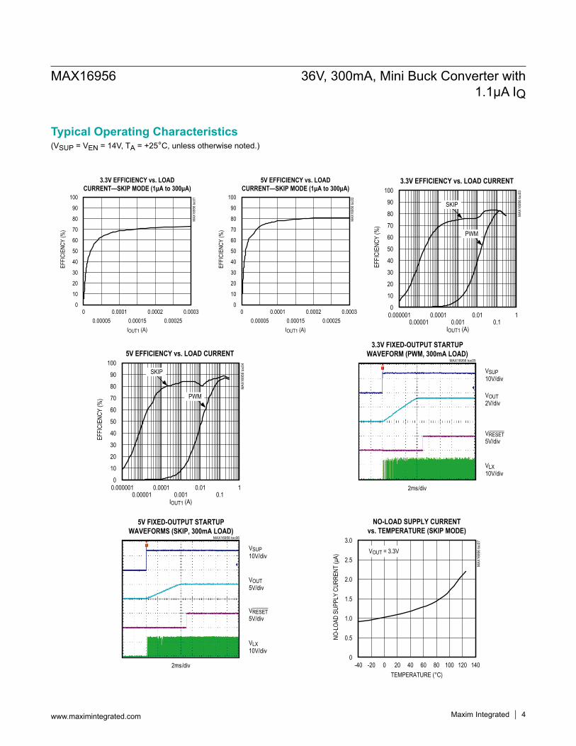
Typical Operating Characteristics(VSUP = VEN = 14V, TA = +25°C, unless otherwise noted.)
3.3V EFFICIENCY vs. LOADCURRENT—SKIP MODE (1μA to 300μA)
MAX
1695
6 to
c01
EFFI
CIEN
CY (%
)
10
20
30
40
50
60
70
80
90
100
0
IOUT1 (A)
0 0.00030.000250.00015
0.00020.00010.00005
5V EFFICIENCY vs. LOADCURRENT—SKIP MODE (1μA to 300μA)
MAX
1695
6 to
c02
IOUT1 (A)
0 0.0003
EFFI
CIEN
CY (%
)
10
20
30
40
50
60
70
80
90
100
0
0.000250.000150.00020.0001
0.00005
3.3V EFFICIENCY vs. LOAD CURRENT
MAX
1695
6 to
c03
EFFI
CIEN
CY (%
)
10
20
30
40
50
60
70
80
90
100
0
SKIP
PWM
IOUT1 (A)
0.000001 10.10.001
0.010.00010.00001
5V EFFICIENCY vs. LOAD CURRENT
MAX
1695
6 to
c04
EFFI
CIEN
CY (%
)
10
20
30
40
50
60
70
80
90
100
0
IOUT1 (A)
0.000001 10.10.001
0.010.00010.00001
SKIP
PWM
5V FIXED-OUTPUT STARTUPWAVEFORMS (SKIP, 300mA LOAD)
MAX16956 toc06
VLX10V/div
VRESET5V/div
VSUP10V/div
VOUT5V/div
2ms/div
3.3V FIXED-OUTPUT STARTUPWAVEFORM (PWM, 300mA LOAD)
MAX16956 toc05
VLX10V/div
VRESET5V/div
VSUP10V/div
VOUT2V/div
2ms/div
NO-LOAD SUPPLY CURRENTvs. TEMPERATURE (SKIP MODE)
MAX
1695
6 to
c07
TEMPERATURE (°C)
NO-L
OAD
SUPP
LY C
URRE
NT (μ
A)
120100806040200-20
0.5
1.0
1.5
2.0
2.5
3.0
0-40 140
VOUT = 3.3V
MAX16956 36V, 300mA, Mini Buck Converter with 1.1µA IQ
Maxim Integrated 5www.maximintegrated.com
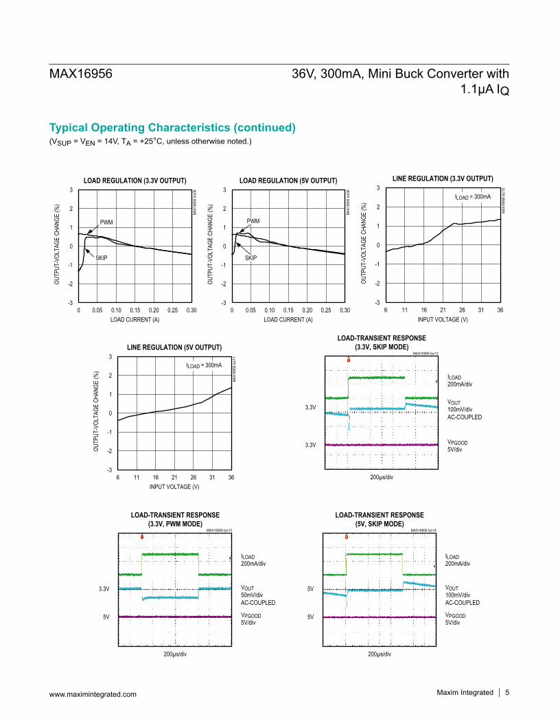
Typical Operating Characteristics (continued)(VSUP = VEN = 14V, TA = +25°C, unless otherwise noted.)
LOAD REGULATION (3.3V OUTPUT)M
AX16
956
toc0
8
LOAD CURRENT (A)
OUTP
UT-V
OLTA
GE C
HANG
E (%
)
0.250.200.150.100.05
-2
-1
0
1
2
3
-30 0.30
PWM
SKIP
LOAD REGULATION (5V OUTPUT)
MAX
1695
6 to
c09
LOAD CURRENT (A)
OUTP
UT-V
OLTA
GE C
HANG
E (%
)
0.250.200.150.100.05
-2
-1
0
1
2
3
-30 0.30
PWM
SKIP
LINE REGULATION (3.3V OUTPUT)
MAX
1695
6 to
c10
INPUT VOLTAGE (V)
OUTP
UT-V
OLTA
GE C
HANG
E (%
)
3126211611
-2
-1
0
1
2
3
-36 36
ILOAD = 300mA
LINE REGULATION (5V OUTPUT)
MAX
1695
6 to
c11
INPUT VOLTAGE (V)
OUTP
UT-V
OLTA
GE C
HANG
E (%
)
3126211611
-2
-1
0
1
2
3
-36 36
ILOAD = 300mA
LOAD-TRANSIENT RESPONSE(3.3V, PWM MODE)
MAX16956 toc13
VPGOOD5V/div
ILOAD200mA/div
3.3V
5V
VOUT50mV/divAC-COUPLED
200µs/div
LOAD-TRANSIENT RESPONSE(3.3V, SKIP MODE)
MAX16956 toc12
VPGOOD5V/div
ILOAD200mA/div
3.3V
3.3V
VOUT100mV/divAC-COUPLED
200µs/div
LOAD-TRANSIENT RESPONSE(5V, SKIP MODE)
MAX16956 toc14
VPGOOD5V/div
ILOAD200mA/div
5V
5V
VOUT100mV/divAC-COUPLED
200µs/div
MAX16956 36V, 300mA, Mini Buck Converter with 1.1µA IQ
Maxim Integrated 6www.maximintegrated.com
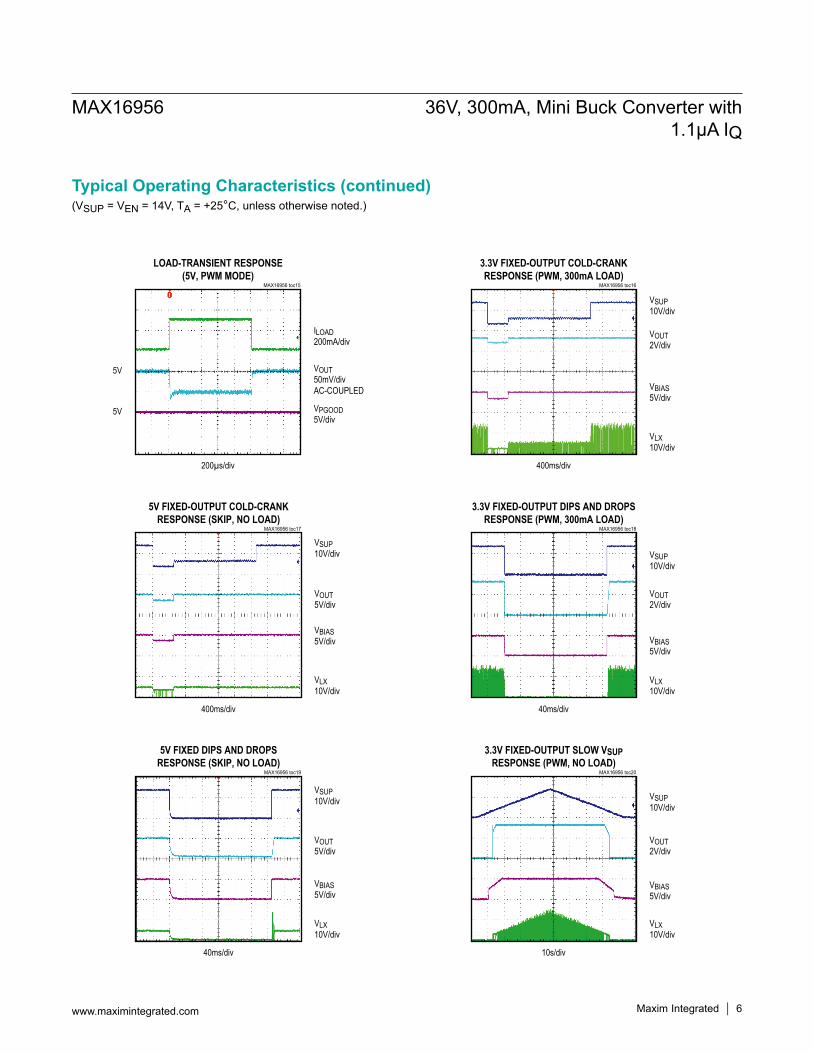
Typical Operating Characteristics (continued)(VSUP = VEN = 14V, TA = +25°C, unless otherwise noted.)
LOAD-TRANSIENT RESPONSE(5V, PWM MODE)
MAX16956 toc15
VPGOOD5V/div
ILOAD200mA/div
5V
5V
VOUT50mV/divAC-COUPLED
200µs/div
5V FIXED-OUTPUT COLD-CRANKRESPONSE (SKIP, NO LOAD)
MAX16956 toc17
VLX10V/div
VSUP10V/div
VOUT5V/div
VBIAS5V/div
400ms/div
5V FIXED DIPS AND DROPSRESPONSE (SKIP, NO LOAD)
MAX16956 toc19
VLX10V/div
VSUP10V/div
VOUT5V/div
VBIAS5V/div
40ms/div
3.3V FIXED-OUTPUT COLD-CRANKRESPONSE (PWM, 300mA LOAD)
MAX16956 toc16
VLX10V/div
VSUP10V/div
VOUT2V/div
VBIAS5V/div
400ms/div
3.3V FIXED-OUTPUT DIPS AND DROPSRESPONSE (PWM, 300mA LOAD)
MAX16956 toc18
VLX10V/div
VSUP10V/div
VOUT2V/div
VBIAS5V/div
40ms/div
3.3V FIXED-OUTPUT SLOW VSUPRESPONSE (PWM, NO LOAD)
MAX16956 toc20
VLX10V/div
VSUP10V/div
VOUT2V/div
VBIAS5V/div
10s/div
MAX16956 36V, 300mA, Mini Buck Converter with 1.1µA IQ
Maxim Integrated 7www.maximintegrated.com
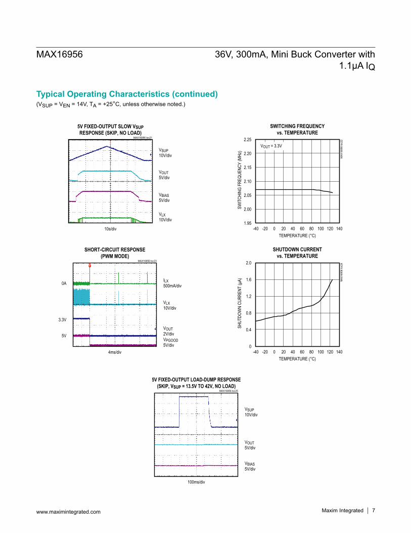
Typical Operating Characteristics (continued)(VSUP = VEN = 14V, TA = +25°C, unless otherwise noted.)
5V FIXED-OUTPUT SLOW VSUPRESPONSE (SKIP, NO LOAD)
MAX16956 toc21
VLX10V/div
VSUP10V/div
VOUT5V/div
VBIAS5V/div
10s/div
SHORT-CIRCUIT RESPONSE(PWM MODE)
MAX16956 toc23
VLX10V/div
ILX500mA/div
VOUT2V/divVPGOOD5V/div
4ms/div
3.3V
5V
0A
5V FIXED-OUTPUT LOAD-DUMP RESPONSE(SKIP, VSUP = 13.5V TO 42V, NO LOAD)
MAX16956 toc25
VSUP10V/div
VOUT5V/div
VBIAS5V/div
100ms/div
SWITCHING FREQUENCYvs. TEMPERATURE
MAX
1695
6 to
c22
TEMPERATURE (°C)SW
ITCH
ING
FREQ
UENC
Y (M
Hz)
120100806040200-20
2.00
2.05
2.10
2.15
2.20
2.25
1.95-40 140
VOUT = 3.3V
SHUTDOWN CURRENTvs. TEMPERATURE
MAX
1695
6 to
c24
TEMPERATURE (°C)
SHUT
DOW
N CU
RREN
T (μ
A)
120100806040200-20
0.4
0.8
1.2
1.6
2.0
0-40 140
MAX16956 36V, 300mA, Mini Buck Converter with 1.1µA IQ
www.maximintegrated.com Maxim Integrated 8
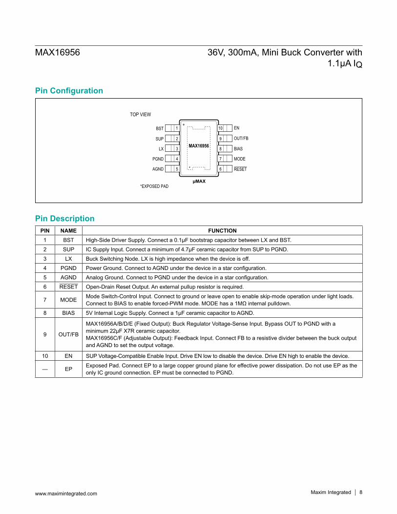
Pin Configuration
Pin DescriptionPIN NAME FUNCTION1 BST High-Side Driver Supply. Connect a 0.1µF bootstrap capacitor between LX and BST.
2 SUP IC Supply Input. Connect a minimum of 4.7µF ceramic capacitor from SUP to PGND.
3 LX Buck Switching Node. LX is high impedance when the device is off.
4 PGND Power Ground. Connect to AGND under the device in a star configuration.
5 AGND Analog Ground. Connect to PGND under the device in a star configuration.
6 RESET Open-Drain Reset Output. An external pullup resistor is required.
7 MODE Mode Switch-Control Input. Connect to ground or leave open to enable skip-mode operation under light loads. Connect to BIAS to enable forced-PWM mode. MODE has a 1MΩ internal pulldown.
8 BIAS 5V Internal Logic Supply. Connect a 1µF ceramic capacitor to AGND.
9 OUT/FB
MAX16956A/B/D/E (Fixed Output): Buck Regulator Voltage-Sense Input. Bypass OUT to PGND with a minimum 22µF X7R ceramic capacitor.MAX16956C/F (Adjustable Output): Feedback Input. Connect FB to a resistive divider between the buck output and AGND to set the output voltage.
10 EN SUP Voltage-Compatible Enable Input. Drive EN low to disable the device. Drive EN high to enable the device.
— EP Exposed Pad. Connect EP to a large copper ground plane for effective power dissipation. Do not use EP as the only IC ground connection. EP must be connected to PGND.
EN
OUT/FB
BIAS
MODE
RESET
SUP
BST
LX
PGND
AGND
+
MAX16956
µMAX
TOP VIEW
*EXPOSED PAD
*
10
9
8
7
6
1
2
3
4
5
MAX16956 36V, 300mA, Mini Buck Converter with 1.1µA IQ
www.maximintegrated.com Maxim Integrated 9
Block Diagram
CURRENT SENSE+
SLOPE COMP
LOGICCONTROL BIAS
CLK
BST
SUP
EN
BIAS
OUT/FB
SW1
SW2
RESET AGND
LX
NOTE 1: FOR INTERNAL FEEDBACK VERSION, SW1 IS OPEN AND SW2 CLOSED. EXTERNAL PIN IS CALLED OUT.
NOTE 2: FOR EXTERNAL FEEDBACK VERSION, SW1 IS CLOSED AND SW2 OPEN. EXTERNAL PIN IS CALLED FB.
PGND
HVLDO
MODE
BANDGAP OSCREF
SOFTSTART
OUTOUTORFB FB
VGOOD COMP
EAMPPWM
MAX16956
MAX16956 36V, 300mA, Mini Buck Converter with 1.1µA IQ
www.maximintegrated.com Maxim Integrated 10
Detailed DescriptionThe MAX16956 is a small, current-mode buck converter that features synchronous rectification and requires no external compensation network. The device operates from a 3.5V to 36V supply voltage and can deliver up to 300mA output current. Frequency is fixed at 2.1MHz, which allows for small external components, reduced output ripple, and guarantees no AM-band interference.The device offers fixed output voltages of 5V and 3.3V. The device also offers adjustable output-voltage versions that can be set between 1V and 10V by using an exter-nal resistive divider. Voltage quality can be monitored by observing the RESET signal. The device offers both forced-PWM and skip mode, with ultra-low-quiescent cur-rent of 1.1µA in skip mode.
DC-DC Converter Control ArchitectureThe device step-down converter uses a PWM peak current-mode control scheme, with a load-line architecture. Peak current-mode control provides several advantages over voltage-mode control, including precise control of the induc-tor current on a cycle-by-cycle basis, simpler compensa-tion, and inherent compensation for line voltage variation.An internal transconductance amplifier establishes an integrated error voltage. The heart of the PWM control-ler is an open-loop comparator: one input is the inte-grated voltage-feedback signal; the other consists of the amplified current-sense signal plus slope-compensation ramp. Integrated high-side current sensing is used, which reduces component count and layout risk by eliminating the need to carefully route sensitive external signals. Error-amplifier compensation is also integrated, once again simplifying the power-supply designer’s task while eliminating external components.At each rising edge of the internal clock, the high-side MOSFET turns on until the PWM comparator trips, the maximum duty cycle is reached, or the peak current limit is reached (see the Current Limit /Short-Circuit Protection section). During this on-time, current ramps up through the inductor, storing energy in a magnetic field and sourcing current to the output. The current-mode feed-back system regulates the peak inductor current as a function of the output-voltage error signal. During the second-half of the cycle, the high-side MOSFET turns off and the low-side MOSFET turns on. The inductor releases the stored energy as the current ramps down,
providing current to the output. The output capacitor stores charge when the inductor current exceeds the required load current and discharges when the inductor current is lower, smoothing the voltage across the load.The device features load-line architecture to reduce the output capacitance needed, potentially saving system cost and size. The output voltage is positioned slightly positive at no load, still within the tolerance window, to take advantage of the fact that any load disturbance is a load step only. This increases the amount of margin available to the undershoot that occurs on a load step, allowing a reduction in the required output capacitance. As the load increases, a small but controlled amount of load regulation (“load-line”) error occurs, so that at heavier loads the voltage is positioned slightly below nominal. This takes advantage of the fact that any load disturbance is load released, increasing the amount of margin available to the overshoot that occurs.The device can operate in either forced-PWM or skip mode. In forced-PWM mode, the converter maintains a constant switching frequency, regardless of load, to allow for easier filtering of the switching noise. The device includes proprietary circuitry that dramatically reduces quiescent current consumption in skip mode, improving light-load efficiency. See the Forced PWM/Skip Modes section for further details.
System Enable (EN)An enable control input (EN) activates the device from its low-power shutdown mode. EN is compatible with inputs from automotive battery level down to 3.5V. The high-voltage compatibility allows EN to be connected to SUP, KEY/KL30, or the inhibit pin (INH) of a CAN transceiver.
Linear Regulator Output (BIAS)The device includes a 5V linear regulator output (BIAS) that provides power to the internal circuit blocks. Connect a 1µF ceramic capacitor from BIAS to AGND. Do not load this pin externally.
Undervoltage LockoutWhen VBIAS drops below the undervoltage-lockout (UVLO) level of VUVLO = 2.8V (typ), the device assumes that the supply voltage is too low for proper operation, so the UVLO circuitry inhibits switching. When VBIAS rises above the UVLO rising threshold, the controller enters the startup sequence and then resumes normal operation.
MAX16956 36V, 300mA, Mini Buck Converter with 1.1µA IQ
www.maximintegrated.com Maxim Integrated 11
Startup and Soft-StartThe device features an internal soft-start timer. The output-voltage soft-start ramp time is 5.4ms (typ). If a short circuit or undervoltage is encountered after the soft-start timer has expired, the device is disabled for 13.4ms (typ) and then reattempts soft-start again. This pattern repeats until the short circuit has been removed.
RESET OutputThe device features an open-drain RESET output to monitor the output voltage. The RESET output requires an external pullup resistor. RESET goes high (high impedance) after the regulator output increases above 92% of the nominal regulated voltage. RESET goes low when the regulator output drops to below 90% of the nominal regulated voltage.
Forced PWM/Skip ModesThe device features a logic-level input (MODE) to switch between forced-PWM and skip modes. Connecting MODE to BIAS enables the forced-PWM operation. Connecting MODE to ground, or leaving unconnected, enables skip-mode operation with ultra-low-quiescent current of 1.1µA. In skip-mode operation, the converter’s switching frequen-cy is load dependent until the output load reaches the skip threshold. At higher load current, the switching frequency does not change and the operating mode is similar to the forced-PWM mode. Skip mode helps improve efficiency in light-load applications by allowing the converter to turn on the high-side switch only when the output voltage falls below a set threshold. As such, the converter does not switch the MOSFETs on and off as often as is the case in the forced-PWM mode. Consequently, the gate charge and switching losses are much lower in skip mode.
Current Limit /Short-Circuit ProtectionThe device has fault protection designed to protect itself from abnormal conditions. If the output is soft shorted (meaning the output is overloaded but over 50% of regulation), cycle-by-cycle current limit limits how high the inductor current goes for any cycle. If the output is hard shorted to ground and the output falls to less than 50% of regulation, the part goes into a mode where it switches until 15 cycles are ended by current limit, then waits for 13.4ms before trying to soft-start again. This mode of operation limits the amount of power dissipated by the device under these conditions. The device also has overtemperature protection. If the die temperature
exceeds approximately 175°C, the device stops switching until the die temperature drops by approximately 15°C and then resumes operation, including going through soft-start again.
Spread-Spectrum OptionThe device has an internal spread-spectrum option to optimize EMI performance. This is factory set on the D, E, and F variants of the device. For spread-spectrum-enabled variants of the device, the operating frequency is varied ±6% centered on 2.1MHz. The modulation signal is a trian gular wave with a period of 230µs at 2.1MHz. Therefore, fSW ramps down 6% and back to 2.1MHz in 115µs and also ramps up 6% and back to 2.1MHz in 115µs. The cycle repeats.
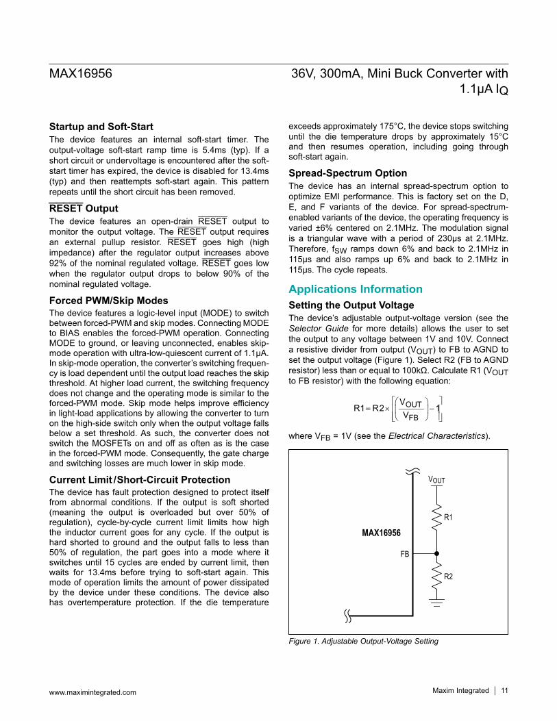
Applications InformationSetting the Output VoltageThe device’s adjustable output-voltage version (see the Selector Guide for more details) allows the user to set the output to any voltage between 1V and 10V. Connect a resistive divider from output (VOUT) to FB to AGND to set the output voltage (Figure 1). Select R2 (FB to AGND resistor) less than or equal to 100kΩ. Calculate R1 (VOUT to FB resistor) with the following equation:
OUT
FB
VR1 R2 1
V
= × −
where VFB = 1V (see the Electrical Characteristics).
Figure 1. Adjustable Output-Voltage Setting
R1
R2
FB
VOUT
MAX16956
MAX16956 36V, 300mA, Mini Buck Converter with 1.1µA IQ
www.maximintegrated.com Maxim Integrated 12
Inductor SelectionThree key inductor parameters must be specified for operation with the device: inductance value (L), inductor saturation current (ISAT), and DC resistance (RDCR). To select inductance value, the ratio of inductor peak-to-peak AC current to DC average current (LIR) must be selected first. A good compromise between size and loss is a 30% peak-to-peak ripple current to average current ratio (LIR = 0.3). The switching frequency, input voltage, output voltage, and selected LIR then determines the inductor value as follows:
OUT SUP OUT
SUP SW OUT
V (V V )L
V f I LIR× −
=× × ×
where VSUP, VOUT, and IOUT are typical values (so that efficiency is optimum for typical conditions). The switching frequency is 2.1MHz. Table 1 lists some of the inductor val-ues for 300mA output current and several output voltages.
Input CapacitorThe input filter capacitor reduces peak currents drawn from the power source and reduces noise and voltage ripple on the input caused by the circuit’s switching. The input capacitor RMS current requirement (IRMS) is defined by the following equation:
OUT SUP OUTRMS LOAD(MAX)
SUP
V (V V )I I
V× −
=
IRMS has a maximum value when the input voltage equals twice the output voltage (VSUP = 2VOUT), so IRMS(MAX) = ILOAD(MAX)/2.Choose an input capacitor that exhibits less than +10°C self-heating temperature rise at the RMS input current for optimal long-term reliability.The input voltage ripple is composed of ΔVQ (caused by the capacitor discharge) and ΔVESR (caused by the ESR of the capacitor). Use low-ESR ceramic capacitors with high ripple current capability at the input. Assume
the contribution from the ESR and capacitor discharge equal to 50%. Calculate the input capacitance and ESR required for a specified input voltage ripple using the following equations:
ESRIN
LOUT
VESR
II
2
∆=
∆+
where:
SUP OUT OUTL
SUP SW
(V V ) VI
V f L− ×
∆ =× ×
and:
OUT OUTIN
Q SW SUP
I D(1 D) VC and D
V f V× −
= =∆ ×
where IOUT is the maximum output current and D is the duty cycle.
Output CapacitorThe output filter capacitor must have low enough ESR to meet output ripple and load transient requirements. The output capacitance must be high enough to absorb the inductor energy while transitioning from full-load to no-load conditions. When using high-capacitance, low-ESR capacitors, the filter capacitor’s ESR dominates the out-put voltage ripple. Therefore, the size of the output capac-itor depends on the maximum ESR required to meet the output voltage ripple (VRIPPLE(P-P)) specifications:
RIPPLE(P P) LOAD(MAX)V ESR I LIR− = × ×
The actual capacitance value required relates to the physical size needed to achieve low ESR, as well as to the chemistry of the capacitor technology. Therefore, the capacitor is usually selected by ESR and voltage rating rather than by capacitance value.When using low-capacity filter capacitors, such as ceram-ic capacitors, size is usually determined by the capacity needed to prevent voltage droop and voltage rise from causing problems during load transients. Generally, once enough capacitance is added to meet the overshoot requirement, undershoot at the rising-load edge is no longer a problem.
Table 1. Inductor Values for 300mA Output Current
VSUP/VOUT (V) 14V/5V 14V/3.3V
INDUCTOR (µH) ILOAD = 300mA 10µH (typ)22µH (max)
10µH (typ)22µH (max)
MAX16956 36V, 300mA, Mini Buck Converter with 1.1µA IQ
www.maximintegrated.com Maxim Integrated 13
PCB Layout GuidelinesCareful PCB layout is critical to achieve low-switching power losses and clean, stable operation. Use a multi-layer board whenever possible for better noise immunity and power dissipation. Follow these guidelines for good PCB layout:1) The input capacitor (4.7µF, see Figures 3 and 4) should
be placed immediately next to the SUP pin of the device. Since the device operates at 2.1MHz switch-ing frequency, this placement is critical for effective decoupling of high-frequency noise from the SUP pin.
2) Solder the exposed pad to a large copper plane area under the device. To effectively use this copper area as heat exchanger between the PCB and ambient, expose the copper area on the top and bottom sides. Add a few small vias or one large via on the copper pad for
efficient heat transfer. Connect the exposed pad to PGND, ideally at the return terminal of the output capacitor.
3) Isolate the power components and high-current path from the sensitive analog circuitry. Doing so is essential to prevent any noise coupling into the analog signals.
4) Keep the high-current paths short, especially at the ground terminals. This practice is essential for stable, jitter-free operation.
5) Connect PGND and AGND together at the return terminal of the output capacitor. Do not connect them anywhere else.
6) Keep the power traces and load connections short. This practice is essential for high efficiency.
7) Place the BIAS capacitor ground next to the AGND pin and connect with a short and wide trace.
MAX16956 36V, 300mA, Mini Buck Converter with 1.1µA IQ
www.maximintegrated.com Maxim Integrated 14
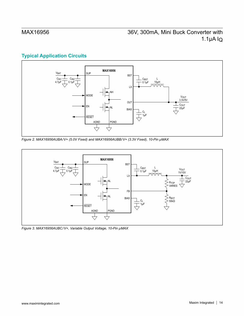
Figure 2. MAX16956AUBA/V+ (5.0V Fixed) and MAX16956AUBB/V+ (3.3V Fixed), 10-Pin µMAX
Figure 3. MAX16956AUBC/V+, Variable Output Voltage, 10-Pin µMAX
Typical Application Circuits
VBAT
CIN14.7µF
CBST0.1µF
COUT22µF
CL1µF
CIN20.1µF
MODE
SUP
EN
RESET
AGND
L10µH
VOUT3.3V/5V
MAX16956
PGND
NL
NH
BIAS
OUT
LX
BST
VBAT
CIN14.7µF
CBST0.1µF
COUT22µF
CL1µF
RTOPVARIES
RBOT50kΩ
CIN20.1µF
MODE
SUP
EN
RESET
AGND
L10µH VOUT
1V/10V
MAX16956
PGND
NL
NL
BIAS
FB
LX
BST
MAX16956 36V, 300mA, Mini Buck Converter with 1.1µA IQ
www.maximintegrated.com Maxim Integrated 15
Package InformationFor the latest package outline information and land patterns (footprints), go to www.maximintegrated.com/packages. Note that a “+”, “#”, or “-” in the package code indicates RoHS status only. Package drawings may show a different suffix character, but the drawing pertains to the package regardless of RoHS status.
Note: Insert the desired suffix letter (from the Selector Guide) into the blank to indicate the output voltage and spread-spectrum option./V denotes an automotive qualified part.+Denotes a lead(Pb)-free/RoHS-compliant package.*EP = Exposed pad.
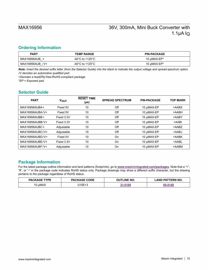
Ordering Information
Selector Guide
PART TEMP RANGE PIN-PACKAGEMAX16956AUB_+ -40°C to +125°C 10 µMAX-EP*
MAX16956AUB_/V+ -40°C to +125°C 10 µMAX-EP*
PACKAGE TYPE PACKAGE CODE OUTLINE NO. LAND PATTERN NO.10 µMAX U10E+3 21-0109 90-0148
PART VOUTRESET TIME
(µs) SPREAD SPECTRUM PIN-PACKAGE TOP MARK
MAX16956AUBA+ Fixed 5V 10 Off 10 µMAX-EP +AABX
MAX16956AUBA/V+ Fixed 5V 10 Off 10 µMAX-EP +AABH
MAX16956AUBB+ Fixed 3.3V 10 Off 10 µMAX-EP +AABY
MAX16956AUBB/V+ Fixed 3.3V 10 Off 10 µMAX-EP +AABI
MAX16956AUBC+ Adjustable 10 Off 10 µMAX-EP +AABZ
MAX16956AUBC/V+ Adjustable 10 Off 10 µMAX-EP +AABJ
MAX16956AUBD/V+ Fixed 5V 10 On 10 µMAX-EP +AABK
MAX16956AUBE/V+ Fixed 3.3V 10 On 10 µMAX-EP +AABL
MAX16956AUBF/V+ Adjustable 10 On 10 µMAX-EP +AABM
Maxim Integrated cannot assume responsibility for use of any circuitry other than circuitry entirely embodied in a Maxim Integrated product. No circuit patent licenses are implied. Maxim Integrated reserves the right to change the circuitry and specifications without notice at any time. The parametric values (min and max limits) shown in the Electrical Characteristics table are guaranteed. Other parametric values quoted in this data sheet are provided for guidance.
Maxim Integrated and the Maxim Integrated logo are trademarks of Maxim Integrated Products, Inc.
MAX16956 36V, 300mA, Mini Buck Converter with 1.1µA IQ
© 2015 Maxim Integrated Products, Inc. 16
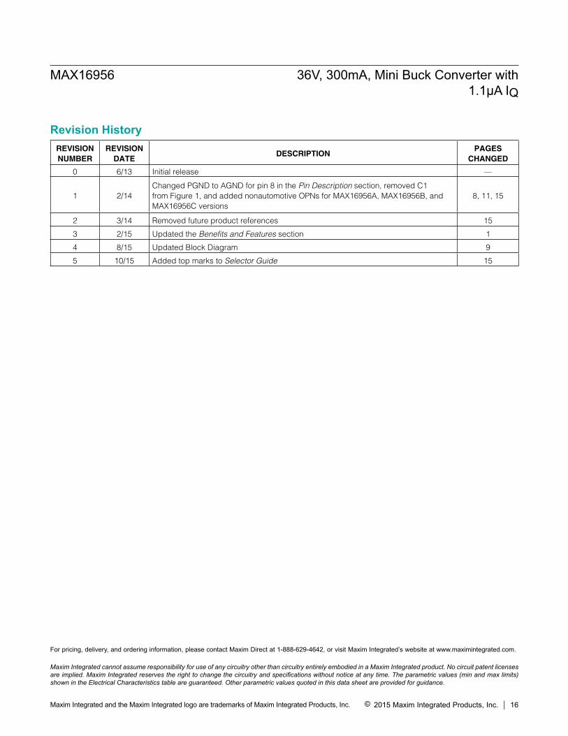
Revision HistoryREVISIONNUMBER
REVISIONDATE
DESCRIPTIONPAGES
CHANGED
0 6/13 Initial release —
1 2/14Changed PGND to AGND for pin 8 in the Pin Description section, removed C1 from Figure 1, and added nonautomotive OPNs for MAX16956A, MAX16956B, and MAX16956C versions
8, 11, 15
2 3/14 Removed future product references 15
3 2/15 Updated the Benefits and Features section 1
4 8/15 Updated Block Diagram 9
5 10/15 Added top marks to Selector Guide 15
For pricing, delivery, and ordering information, please contact Maxim Direct at 1-888-629-4642, or visit Maxim Integrated’s website at www.maximintegrated.com.


![A note on UP-hyperalgebrasjahla.hatef.ac.ir/article_107891_a478986374d101cc340b08a...the relationship between hyper BCK-ideals and weak hyper BCK-ideals. Borzooei et al. [4] introduced](https://img.pdfslide.net/doc/110x75/5fb480fc2d407341e0019dd5/a-note-on-up-the-relationship-between-hyper-bck-ideals-and-weak-hyper-bck-ideals.jpg)