Embed Size (px)
Citation preview

General DescriptionThe MAX16833, MAX16833B, MAX16833C, MAX16833D, and MAX16833G are peak current-mode-controlled LED drivers for boost, buck-boost, SEPIC, flyback, and high-side buck topologies. A dimming driver designed to drive an external p-channel in series with the LED string pro-vides wide-range dimming control. This feature provides extremely fast PWM current switching to the LEDs with no transient overvoltage or undervoltage conditions. In addition to PWM dimming, the ICs provide analog dimming using a DC input at ICTRL. The ICs sense the LED current at the high side of the LED string.A single resistor from RT/SYNC to ground sets the switching frequency from 100kHz to 1MHz, while an external clock signal capacitively coupled to RT/SYNC allows the ICs to synchronize to an external clock. In the MAX16833/C/G, the switching frequency can be dithered for spread-spectrum applications. The MAX16833B/D instead provide a 1.64V reference voltage with a 2% tolerance.The ICs operate over a wide 5V to 65V supply range and include a 3A sink/source gate driver for driving a power MOSFET in high-power LED driver applications. Additional features include a fault-indicator output (FLT) for short or overtemperature conditions and an overvolt-age-protection sense input (OVP) for overvoltage protec-tion. High-side current sensing combined with a p-channel dimming MOSFET allow the positive terminal of the LED string to be shorted to the positive input terminal or to the negative input terminal without any damage. This is a unique feature of the ICs.
Applications Automotive Exterior Lighting:
High-Beam/Low-Beam/Signal/Position Lights Daytime Running Lights (DRLs) Fog Light and Adaptive Front Light Assemblies
Commercial, Industrial, and Architectural Lighting
Benefits and Features Integration Minimizes BOM for High-Brightness LED
Driver with a Wide Input Range Saving Space and Cost• +5V to +65V Wide Input Voltage Range with a
Maximum 65V Boost Output• Integrated High-Side pMOS Dimming MOSFET
Driver (Allows Single-Wire Connection to LEDs)• ICTRL Pin for Analog Dimming• Integrated High-Side Current-Sense Amplifier• Full-Scale, High-Side, Current-Sense Voltage of
200mV Simple to Optimize for Efficiency, Board Space, and
Input Operating Range• Boost, SEPIC, and Buck-Boost Single-Channel
LED Drivers• 2% Accurate 1.64V Reference (MAX16833B/D)• Programmable Operating Frequency (100kHz to
1MHz) with Synchronization Capability• Frequency Dithering for Spread-Spectrum
Applications (MAX16833/C/G)• Thermally Enhanced 5mm x 4.4mm, 16-Pin
TSSOP Package with Exposed Pad Protection Features and Wide Temperature Range
Increase System Reliability• Short-Circuit, Overvoltage, and Thermal Protection• Fault-Indicator Output• -40°C to +125°C Operating Temperature Range
19-5187; Rev 12; 8/17
Ordering Information appears at end of data sheet.
PWMDIM
IN NDRV
CS
OVP
ISENSE+ISENSE-
PGND
6V TO 18VWITH LOAD
DUMP UPTO 70V
LED+
LED-
PWMDIM
DIMOUT
MAX16833
Simplified Operating Circuit
MAX16833/MAX16833B/C/D/G High-Voltage HB LED Drivers with Integrated High-Side Current Sense
EVALUATION KIT AVAILABLE

IN to PGND .......................................................... -0.3V to +70VISENSE+, ISENSE-, DIMOUT to PGND .............. -0.3V to +80VDIMOUT to ISENSE+ ..............................................-9V to +0.3VISENSE- to ISENSE+ ...........................................-0.6V to +0.3VPGND to SGND ....................................................-0.3V to +0.3VVCC to PGND ..........................................................-0.3V to +9VNDRV to PGND ........................................ -0.3V to (VCC + 0.3V)OVP, PWMDIM, COMP, LFRAMP, REF, ICTRL,
RT/SYNC, FLT to SGND ..................................-0.3V to +6.0VCS to PGND .........................................................-0.3V to +6.0VContinuous Current on IN ................................................100mA
Peak Current on NDRV ........................................................ Q3AContinuous Current on NDRV ....................................... Q100mAShort-Circuit Duration on VCC ...................................ContinuousContinuous Power Dissipation (TA = +70NC) 16-Pin TSSOP (derate 26.1mW/NC above +70NC) .....2089mWOperating Temperature Range ....................... -40NC to +125NCJunction Temperature ......................................................+150NCStorage Temperature Range ............................ -65NC to +150NCLead Temperature (soldering, 10s) .................................+300NCSoldering Temperature (reflow) .......................................+260NC
16 TSSOP Junction-to-Ambient Thermal Resistance (qJA) .......38.3°C/W Junction-to-Case Thermal Resistance (qJC) .................3°C/W
(VIN = 12V, RRT = 12.4kI, CIN = CVCC = 1µF, CLFRAMP/CREF = 0.1µF, NDRV = COMP = DIMOUT = PWMDIM = FLT = unconnected, VOVP = VCS = VPGND = VSGND = 0V, VISENSE+ = VISENSE- = 45V, VICTRL = 1.40V, TA = TJ = -40NC to +125NC, unless otherwise noted. Typical values are at TA = +25NC.) (Note 2)
PARAMETER SYMBOL CONDITIONS MIN TYP MAX UNITS
SYSTEM SPECIFICATIONSOperational Supply Voltage VIN 5 65 V
Supply Current IINQPWMDIM = 0, no switching 1.5 2.5
mASwitching 2.5 4
Undervoltage Lockout (UVLO)UVLORIN VIN rising 4.2 4.55 4.85
VUVLOFIN VIN falling, IVCC = 35mA 4.05 4.3 4.65
UVLO Hysteresis 250 mVStartup Delay tSTART_DELAY During power-up 410 FsUVLO Falling Delay tFALL_DELAY During power-down 3.3 FsVCC LDO REGULATOR
Regulator Output Voltage VCC0.1mA P IVCC P 50mA, 9V P VIN P 14V
6.75 6.95 7.15 V14V P VIN P 65V, IVCC = 10mA
Dropout Voltage VDOVCC IVCC = 50mA, VIN = 5V 0.15 0.35 VShort-Circuit Current IMAXVCC VCC = 0V, VIN = 5V 55 100 150 mAOSCILLATOR (RT/SYNC)Switching Frequency Range fSW 100 1000 kHzBias Voltage at RT/SYNC VRT 1 V
Maximum Duty Cycle DMAX
VCS = 0V; MAX16833/MAX16833B only 87.5 88.5 89.5%VCS = 0V; MAX16833C/MAX16833D/
MAX16833G only 93 94 95
Oscillator Frequency Accuracy -5 +5 %
Stresses beyond those listed under “Absolute Maximum Ratings” may cause permanent damage to the device. These are stress ratings only, and functional opera-tion of the device at these or any other conditions beyond those indicated in the operational sections of the specifications is not implied. Exposure to absolute maximum rating conditions for extended periods may affect device reliability.
Electrical Characteristics
Absolute Maximum Ratings
Note 1: Package thermal resistances were obtained using the method described in JEDEC specification JESD51-7, using a four-layer board. For detailed information on package thermal considerations, refer to www.maximintegrated.com/thermal-tutorial.
Package Thermal Characteristics (Note 1)
www.maximintegrated.com Maxim Integrated 2
MAX16833/MAX16833B/C/D/G High-Voltage HB LED Drivers with Integrated High-Side Current Sense
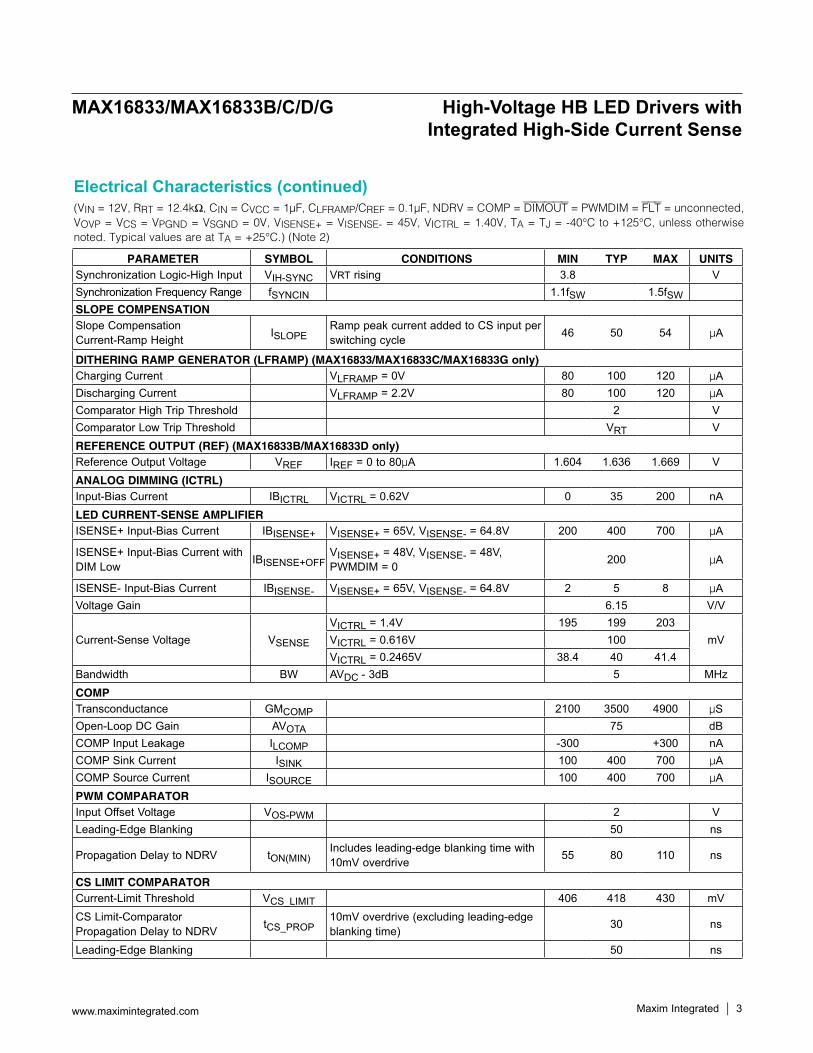
(VIN = 12V, RRT = 12.4kI, CIN = CVCC = 1µF, CLFRAMP/CREF = 0.1µF, NDRV = COMP = DIMOUT = PWMDIM = FLT = unconnected, VOVP = VCS = VPGND = VSGND = 0V, VISENSE+ = VISENSE- = 45V, VICTRL = 1.40V, TA = TJ = -40NC to +125NC, unless otherwise noted. Typical values are at TA = +25NC.) (Note 2)
PARAMETER SYMBOL CONDITIONS MIN TYP MAX UNITSSynchronization Logic-High Input VIH-SYNC VRT rising 3.8 VSynchronization Frequency Range fSYNCIN 1.1fSW 1.5fSWSLOPE COMPENSATIONSlope CompensationCurrent-Ramp Height ISLOPE
Ramp peak current added to CS input per switching cycle 46 50 54 FA
DITHERING RAMP GENERATOR (LFRAMP) (MAX16833/MAX16833C/MAX16833G only)Charging Current VLFRAMP = 0V 80 100 120 FADischarging Current VLFRAMP = 2.2V 80 100 120 FAComparator High Trip Threshold 2 VComparator Low Trip Threshold VRT VREFERENCE OUTPUT (REF) (MAX16833B/MAX16833D only)Reference Output Voltage VREF IREF = 0 to 80FA 1.604 1.636 1.669 VANALOG DIMMING (ICTRL)Input-Bias Current IBICTRL VICTRL = 0.62V 0 35 200 nALED CURRENT-SENSE AMPLIFIERISENSE+ Input-Bias Current IBISENSE+ VISENSE+ = 65V, VISENSE- = 64.8V 200 400 700 FA
ISENSE+ Input-Bias Current with DIM Low IBISENSE+OFF
VISENSE+ = 48V, VISENSE- = 48V,PWMDIM = 0 200 FA
ISENSE- Input-Bias Current IBISENSE- VISENSE+ = 65V, VISENSE- = 64.8V 2 5 8 FAVoltage Gain 6.15 V/V
Current-Sense Voltage VSENSE
VICTRL = 1.4V 195 199 203mVVICTRL = 0.616V 100
VICTRL = 0.2465V 38.4 40 41.4Bandwidth BW AVDC - 3dB 5 MHzCOMPTransconductance GMCOMP 2100 3500 4900 FSOpen-Loop DC Gain AVOTA 75 dBCOMP Input Leakage ILCOMP -300 +300 nACOMP Sink Current ISINK 100 400 700 FACOMP Source Current ISOURCE 100 400 700 FAPWM COMPARATORInput Offset Voltage VOS-PWM 2 VLeading-Edge Blanking 50 ns
Propagation Delay to NDRV tON(MIN)Includes leading-edge blanking time with 10mV overdrive 55 80 110 ns
CS LIMIT COMPARATORCurrent-Limit Threshold VCS_LIMIT 406 418 430 mVCS Limit-ComparatorPropagation Delay to NDRV tCS_PROP
10mV overdrive (excluding leading-edge blanking time) 30 ns
Leading-Edge Blanking 50 ns
Electrical Characteristics (continued)
www.maximintegrated.com Maxim Integrated 3
MAX16833/MAX16833B/C/D/G High-Voltage HB LED Drivers with Integrated High-Side Current Sense
(VIN = 12V, RRT = 12.4kI, CIN = CVCC = 1µF, CLFRAMP/CREF = 0.1µF, NDRV = COMP = DIMOUT = PWMDIM = FLT = unconnected, VOVP = VCS = VPGND = VSGND = 0V, VISENSE+ = VISENSE- = 45V, VICTRL = 1.40V, TA = TJ = -40NC to +125NC, unless otherwise noted. Typical values are at TA = +25NC.) (Note 2)
PARAMETER SYMBOL CONDITIONS MIN TYP MAX UNITS
GATE DRIVER (NDRV)Peak Pullup Current INDRVPU VCC = 7V, VNDRV = 0V 3 APeak Pulldown Current INDRVPD VCC = 7V, VNDRV = 7V 3 ARise Time tr CNDRV = 10nF 30 nsFall Time tf CNDRV = 10nF 30 nsRDSON Pulldown nMOS RNDRVON VCOMP = 0V, ISINK = 100mA 0.25 0.6 1.1 I
PWM DIMMING (PWMDIM)ON Threshold VPWMON 1.19 1.225 1.26 VHysteresis VPWMHY 70 mVPullup Resistance RPWMPU 1.7 3 4.5 MI
PWMDIM to LED Turn-Off Time PWMDIM falling edge to rising edge on DIMOUT, CDIMOUT = 7nF 2 Fs
PWMDIM to LED Turn-On Time PWMDIM rising edge to falling edge on DIMOUT, CDIMOUT = 7nF 3 Fs
pMOS GATE DRIVER (DIMOUT)
Peak Pullup Current IDIMOUTPUVPWMDIM = 0V,VISENSE+ - VDIMOUT = 7V 25 50 80 mA
Peak Pulldown Current IDIMOUTPD VISENSE+ - VDIMOUT = 0V 10 25 45 mA
DIMOUT Low Voltage with Respect to VISENSE+
-8.7 -7.4 -6.3 V
OVERVOLTAGE PROTECTION (OVP)Threshold VOVPOFF VOVP rising 1.19 1.225 1.26 VHysteresis VOVPHY 70 mVInput Leakage ILOVP VOVP = 1.235V -300 +300 nASHORT-CIRCUIT HICCUP MODE (not present in the MAX16833G)Short-Circuit Threshold VSHORT-HIC (VISENSE+ - VISENSE-) rising 285 298 310 mV
Hiccup Time tHICCUP 8192 Clock Cycles
Delay in Short-Circuit Hiccup Activation 1 Fs
BUCK-BOOST SHORT-CIRCUIT DETECTBuck-Boost Short-Circuit Threshold VSHORT-BB (VISENSE+ - VIN) falling, VIN = 12V 1.15 1.55 1.9 V
Delay in FLT Assertion from Buck-Boost Short-Circuit Condition
tDEL-BB-SHRTCounter increments only when VPWMDIM > VPWMON
8192 Clock Cycles
Delay in FLT Deassertion After Buck-Boost Short Circuit is Removed (Consecutive Clock-Cycle Count)
Counter increments only when VPWMDIM > VPWMON
8192 Clock Cycles
Electrical Characteristics (continued)
www.maximintegrated.com Maxim Integrated 4
MAX16833/MAX16833B/C/D/G High-Voltage HB LED Drivers with Integrated High-Side Current Sense

(VIN = 12V, RRT = 12.4kI, CIN = CVCC = 1µF, CLFRAMP/CREF = 0.1µF, NDRV = COMP = DIMOUT = PWMDIM = FLT = unconnected, VOVP = VCS = VPGND = VSGND = 0V, VISENSE+ = VISENSE- = 45V, VICTRL = 1.40V, TA = TJ = -40NC to +125NC, unless otherwise noted. Typical values are at TA = +25NC.) (Note 2)
(VIN = +12V, CVIN = CVCC = 1FF, CLFRAMP/CREF = 0.1FF, TA = +25NC, unless otherwise noted.)
Note 2: All devices are 100% tested at TA = +25NC. Limits over temperature are guaranteed by design.
PARAMETER SYMBOL CONDITIONS MIN TYP MAX UNITS
OPEN-DRAIN FAULT (FLT)Output Voltage Low VOL-FLT VIN = 4.75V, VOVP = 2V, and ISINK = 5mA 40 200 mVOutput Leakage Current VFLT = 5V 1 FATHERMAL SHUTDOWNThermal-Shutdown Temperature Temperature rising +160 NCThermal-Shutdown Hysteresis 10 NC
IN RISING/FALLING UVLO THRESHOLDvs. TEMPERATURE
MAX
1683
3 to
c01
TEMPERATURE (°C)
IN R
ISIN
G/FA
LLIN
G UV
LO T
HRES
HOLD
(V)
11085603510-15
4.3
4.4
4.5
4.6
4.7
4.8
4.2-40 125
VIN RISING
VIN FALLING
QUIESCENT CURRENTvs. TEMPERATURE
MAX
1683
3 to
c02
TEMPERATURE (°C)
QUIE
SCEN
T CU
RREN
T (m
A)
11085603510-15
1
2
3
4
0-40 125
VPWMDIM = 0V
QUIESCENT CURRENT vs. VIN
MAX
1683
3 to
c03
VIN (V)
QUIE
SCEN
T CU
RREN
T (m
A)
10
0.5
1.0
1.5
2.0
2.5
01 100
VIN ~ 4.6V
VPWMDIM = 0V
VCC vs. IVCC
MAX
1683
3 to
c04
IVCC (mA)
V CC
(V)
45403530252015105
6.80
6.85
6.90
6.95
7.00
6.750 50
VCC vs. TEMPERATURE
MAX
1683
3 to
c05
TEMPERATURE (°C)
V CC
(V)
11085603510-15
6.80
6.85
6.90
6.95
7.00
7.05
7.10
6.75-40 125
MAX
1683
3 to
c06
TEMPERATURE (°C)
11085603510-15
-8.2
-7.7
-7.2
-6.7
-6.2
-8.7-40 125
DIMOUT (WITH RESPECT TO ISENSE+)vs. TEMPERATURE
DIM
OUT
(WIT
H RE
SPEC
T TO
ISEN
SE+)
(V)
Electrical Characteristics (continued)
Typical Operating Characteristics
www.maximintegrated.com Maxim Integrated 5
MAX16833/MAX16833B/C/D/G High-Voltage HB LED Drivers with Integrated High-Side Current Sense
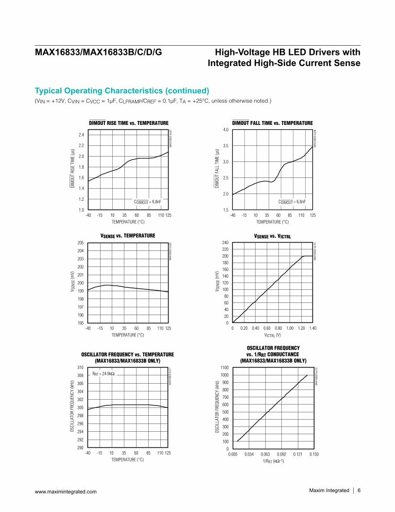
(VIN = +12V, CVIN = CVCC = 1FF, CLFRAMP/CREF = 0.1FF, TA = +25NC, unless otherwise noted.)
MAX
1683
3 to
c07
TEMPERATURE (°C)
DIM
OUT
RISE
TIM
E (µ
s)
11085-15 10 35 60
1.2
1.4
1.6
1.8
2.0
2.2
2.4
1.0-40 125
DIMOUT RISE TIME vs. TEMPERATURE
CDIMOUT = 6.8nF
MAX
1683
3 to
c08
TEMPERATURE (°C)
11085603510-15
2.0
2.5
3.0
3.5
4.0
1.5-40 125
DIMOUT FALL TIME vs. TEMPERATURE
DIM
OUT
FALL
TIM
E (µ
s)
CDIMOUT = 6.8nF
VSENSE vs. TEMPERATURE
MAX
1683
3 to
c09
TEMPERATURE (°C)
V SEN
SE (m
V)
1108535 6010-15
196
197
198
199
200
201
202
203
204
205
195-40 125
VSENSE vs. VICTRL
MAX
1683
3 to
c10
VICTRL (V)
V SEN
SE (m
V)
1.201.000.60 0.800.400.20
20
40
60
80
100
120
140
160
180
200
220
240
00 1.40
OSCILLATOR FREQUENCYvs. 1/RRT CONDUCTANCE
(MAX16833/MAX16833B ONLY)
MAX
1683
3 to
c12
1/RRT (kI-1)
OSCI
LLAT
OR F
REQU
ENCY
(kHz
)
0.1210.0920.0630.034
100
200
300
400
500
600
700
800
900
1000
1100
00.005 0.150
OSCILLATOR FREQUENCY vs. TEMPERATURE(MAX16833/MAX16833B ONLY)
MAX
1683
3 to
c11
TEMPERATURE (°C)
OSCI
LLAT
OR F
REQU
ENCY
(kHz
)
1108535 6010-15
292
294
296
298
300
302
304
306
308
310
290-40 125
RRT = 24.9kI
Typical Operating Characteristics (continued)
Maxim Integrated 6www.maximintegrated.com
MAX16833/MAX16833B/C/D/G High-Voltage HB LED Drivers with Integrated High-Side Current Sense
(VIN = +12V, CVIN = CVCC = 1FF, CLFRAMP/CREF = 0.1FF, TA = +25NC, unless otherwise noted.)
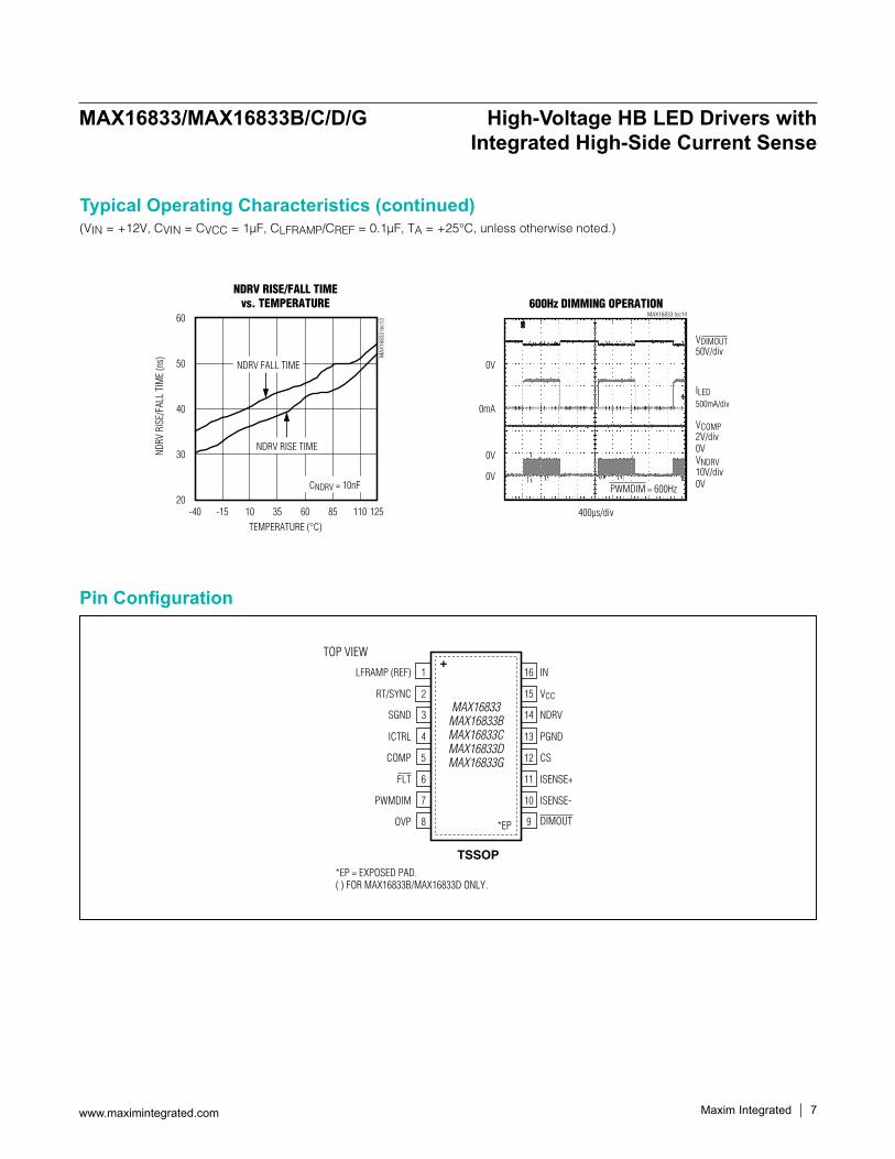
NDRV RISE/FALL TIMEvs. TEMPERATURE
MAX
1683
3 to
c13
TEMPERATURE (°C)
NDRV
RIS
E/FA
LL T
IME
(ns)
11085603510-15
30
40
50
60
20-40 125
NDRV RISE TIME
CNDRV = 10nF
NDRV FALL TIME
600Hz DIMMING OPERATIONMAX16833 toc14
ILED500mA/div
0V
0V
0V
0V
0mA
0V
VCOMP2V/div
VNDRV10V/div
400µs/div
VDIMOUT50V/div
PWMDIM = 600Hz
16
15
14
13
12
11
10
1
2
3
4
5
6
7
IN
VCC
NDRV
PGNDICTRL
SGND
RT/SYNC
LFRAMP (REF)
TOP VIEW
MAX16833MAX16833BMAX16833CMAX16833DMAX16833G CS
ISENSE+
ISENSE-PWMDIM
98OVP *EP
*EP = EXPOSED PAD.( ) FOR MAX16833B/MAX16833D ONLY.
COMP
TSSOP
+
FLT
DIMOUT
Typical Operating Characteristics (continued)
Pin Configuration
Maxim Integrated 7www.maximintegrated.com
MAX16833/MAX16833B/C/D/G High-Voltage HB LED Drivers with Integrated High-Side Current Sense
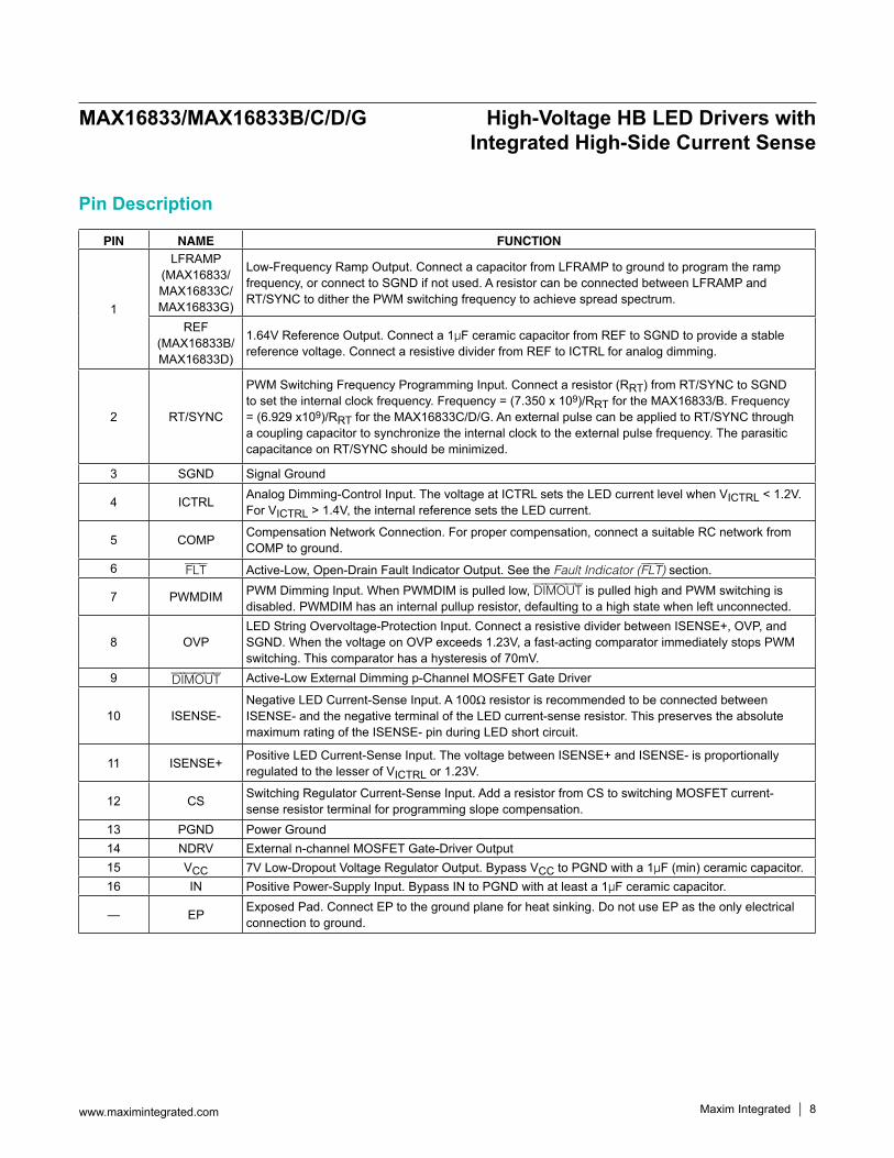
PIN NAME FUNCTION
1
LFRAMP(MAX16833/MAX16833C/MAX16833G)
Low-Frequency Ramp Output. Connect a capacitor from LFRAMP to ground to program the ramp frequency, or connect to SGND if not used. A resistor can be connected between LFRAMP and RT/SYNC to dither the PWM switching frequency to achieve spread spectrum.
REF(MAX16833B/MAX16833D)
1.64V Reference Output. Connect a 1FF ceramic capacitor from REF to SGND to provide a stable reference voltage. Connect a resistive divider from REF to ICTRL for analog dimming.
2 RT/SYNC
PWM Switching Frequency Programming Input. Connect a resistor (RRT) from RT/SYNC to SGND to set the internal clock frequency. Frequency = (7.350 x 10⁹)/RRT for the MAX16833/B. Frequency = (6.929 x10⁹)/RRT for the MAX16833C/D/G. An external pulse can be applied to RT/SYNC through a coupling capacitor to synchronize the internal clock to the external pulse frequency. The parasitic capacitance on RT/SYNC should be minimized.
3 SGND Signal Ground
4 ICTRL Analog Dimming-Control Input. The voltage at ICTRL sets the LED current level when VICTRL < 1.2V. For VICTRL > 1.4V, the internal reference sets the LED current.
5 COMP Compensation Network Connection. For proper compensation, connect a suitable RC network from COMP to ground.
6 FLT Active-Low, Open-Drain Fault Indicator Output. See the Fault Indicator (FLT) section.
7 PWMDIM PWM Dimming Input. When PWMDIM is pulled low, DIMOUT is pulled high and PWM switching is disabled. PWMDIM has an internal pullup resistor, defaulting to a high state when left unconnected.
8 OVPLED String Overvoltage-Protection Input. Connect a resistive divider between ISENSE+, OVP, and SGND. When the voltage on OVP exceeds 1.23V, a fast-acting comparator immediately stops PWM switching. This comparator has a hysteresis of 70mV.
9 DIMOUT Active-Low External Dimming p-Channel MOSFET Gate Driver
10 ISENSE-Negative LED Current-Sense Input. A 100I resistor is recommended to be connected between ISENSE- and the negative terminal of the LED current-sense resistor. This preserves the absolute maximum rating of the ISENSE- pin during LED short circuit.
11 ISENSE+ Positive LED Current-Sense Input. The voltage between ISENSE+ and ISENSE- is proportionally regulated to the lesser of VICTRL or 1.23V.
12 CS Switching Regulator Current-Sense Input. Add a resistor from CS to switching MOSFET current- sense resistor terminal for programming slope compensation.
13 PGND Power Ground14 NDRV External n-channel MOSFET Gate-Driver Output15 VCC 7V Low-Dropout Voltage Regulator Output. Bypass VCC to PGND with a 1FF (min) ceramic capacitor.16 IN Positive Power-Supply Input. Bypass IN to PGND with at least a 1FF ceramic capacitor.
— EP Exposed Pad. Connect EP to the ground plane for heat sinking. Do not use EP as the only electrical connection to ground.
Pin Description
www.maximintegrated.com Maxim Integrated 8
MAX16833/MAX16833B/C/D/G High-Voltage HB LED Drivers with Integrated High-Side Current Sense

MAX16833MAX16833C
IN
CS
REF
ICTRL
ISENSE+
ISENSE-
PWMDIM
OVP
RT/SYNC
VCC
VCC
NDRV
PGND
RESETDOMINANT
PWMCOMP
MAXDUTY CYCLE
S
R
Q
S
R
Q
UVLO
UVLO
RT OSCILLATOR
SLOPECOMPENSATION
1.64V (80µA)REFERENCE
CS/PWMBLANKING
0.42V
6.15
6.15 x 0.3V
1µs DELAY
8192 x tOSCHICCUP TIMER
VISENSE+ - 7V
ISENSE+SYNC
BUCK-BOOSTSHORT DETECTION
TSHDN
SGND
FLT
DIMOUT
COMP
VBG
3.3V
VBG
3MI
GM
VBG
LPFMINOUT
2V
THERMALSHUTDOWN
LVSH
TSHDN
5.7V
5V5V VBG
5V REG BG 7V LDO
200kI
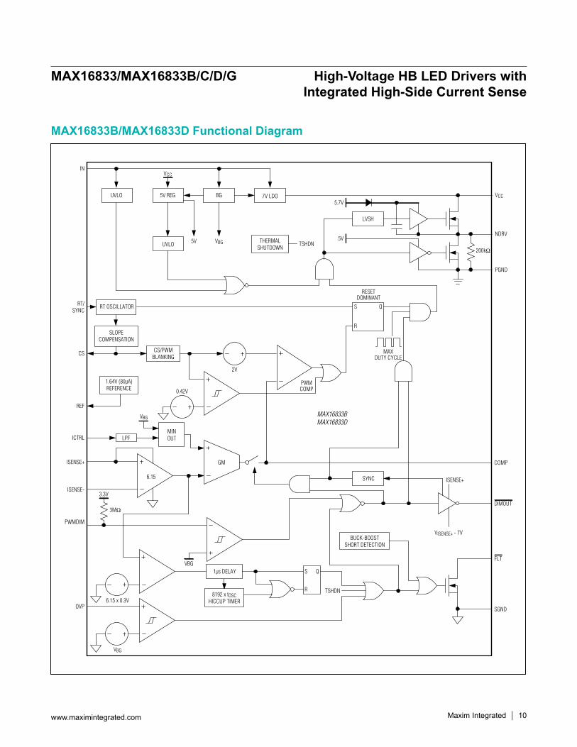
MAX16833/MAX16833C Functional Diagram
www.maximintegrated.com Maxim Integrated 9
MAX16833/MAX16833B/C/D/G High-Voltage HB LED Drivers with Integrated High-Side Current Sense
MAX16833BMAX16833D
IN
CS
REF
ICTRL
ISENSE+
ISENSE-
PWMDIM
OVP
RT/SYNC
VCC
VCC
NDRV
PGND
RESETDOMINANT
PWMCOMP
MAXDUTY CYCLE
S
R
Q
S
R
Q
UVLO
UVLO
RT OSCILLATOR
SLOPECOMPENSATION
1.64V (80µA)REFERENCE
CS/PWMBLANKING
0.42V
6.15
6.15 x 0.3V
1µs DELAY
8192 x tOSCHICCUP TIMER
VISENSE+ - 7V
ISENSE+SYNC
BUCK-BOOSTSHORT DETECTION
TSHDN
SGND
FLT
DIMOUT
COMP
VBG
3.3V
VBG
3MI
GM
VBG
LPFMINOUT
2V
THERMALSHUTDOWN
LVSH
TSHDN
5.7V
5V5V VBG
5V REG BG 7V LDO
200kI
MAX16833B/MAX16833D Functional Diagram
www.maximintegrated.com Maxim Integrated 10
MAX16833/MAX16833B/C/D/G High-Voltage HB LED Drivers with Integrated High-Side Current Sense
MAX16833G
IN
CS
LFRAMP
ICTRL
ISENSE+
ISENSE-
PWMDIM
OVP
RT/SYNC
VCC
VCC
NDRV
PGND
RESETDOMINANT
PWMCOMP
MAXDUTY CYCLE
S
R
Q
UVLO
UVLO
RT OSCILLATOR
SLOPECOMPENSATION
RAMPGENERATION
CS/PWMBLANKING
0.42V
6.15
VISENSE+ - 7V
ISENSE+SYNC
BUCK-BOOSTSHORT DETECTION
SGND
FLT
DIMOUT
COMP
VBG
3.3V
VBG
3MI
GM
VBG
LPFMINOUT
2V
THERMALSHUTDOWN
LVSH
TSHDN
5.7V
5V5V VBG
5V REG BG 7V LDO
200kI
TSHDN
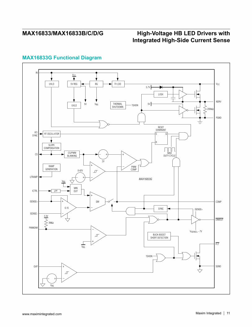
MAX16833G Functional Diagram
www.maximintegrated.com Maxim Integrated 11
MAX16833/MAX16833B/C/D/G High-Voltage HB LED Drivers with Integrated High-Side Current Sense

Detailed DescriptionThe MAX16833, MAX16833B, MAX16833C, MAX16833D, and MAX16833G are peak current-mode-controlled LED drivers for boost, buck-boost, SEPIC, flyback, and high-side buck topologies. A low-side gate driver capable of sinking and sourcing 3A can drive a power MOSFET in the 100kHz to 1MHz frequency range. Constant-frequency peak current-mode control is used to control the duty cycle of the PWM controller that drives the power MOSFET. Externally programmable slope compensation prevents subharmonic oscillations for duty cycles exceeding 50% when the inductor is operating in continuous conduction mode. Most of the power for the internal control circuitry inside the ICs is provided from an internal 5V regulator. The gate drive for the low-side switching MOSFET is provided by a separate VCC regulator. A dimming driver designed to drive an external p-channel in series with the LED string provides wide-range dimming control. This dimming driver is powered by a separate unconnected reference -7V regulator. This feature provides extremely fast PWM current switching to the LEDs with no transient overvoltage or undervoltage conditions. In addition to PWM dimming, the ICs provide analog dimming using a DC input at the ICTRL input.A single resistor from RT/SYNC to ground sets the switching frequency from 100kHz to 1MHz, while an external clock signal capacitively coupled to RT/SYNC allows the ICs to synchronize to an external clock. The switching frequency can be dithered for spread-spectrum applications by connecting the LFRAMP output to RT/SYNC through an external resistor in the MAX16833/C/G. In the MAX16833B/D, the LFRAMP output is replaced by a REF output, which provides a regulated 1.64V, 2% accurate reference that can be used with a resistive divider from REF to ICTRL to set the LED current. The maximum cur-rent from the REF output cannot exceed 80FA.Additional features include a fault-indicator output (FLT) for short, overvoltage, or overtemperature conditions and an overvoltage-protection (OVP) sense input for overvoltage protection. In case of LED string short, for a buck-boost configuration, the short-circuit current is equal to the programmed LED current. In the case of boost configuration, the ICs enter hiccup mode with automatic recovery from short circuit. In the MAX16833G, the hiccup mode is disabled. The MAX16833G should not be used in boost applications.
UVLOThe ICs feature undervoltage lockout (UVLO) using the positive power-supply input (IN). The ICs are enabled when VIN exceeds the 4.6V (typ) threshold and are dis-abled when VIN drops below the 4.35V (typ) threshold. The UVLO is internally fixed and cannot be adjusted. There is a startup delay of 300µs (typ) + 64 switching clock cycles on power-up after the UVLO threshold is crossed. There is a 3.3Fs delay on power-down on the falling edge of the UVLO.
Dimming MOSFET Driver (DIMOUT)The ICs require an external p-channel MOSFET for PWM dimming. For normal operation, connect the gate of the MOSFET to the output of the dimming driver (DIMOUT). The dimming driver can sink up to 25mA or source up to 50mA of peak current for fast charging and discharging of the p-MOSFET gate. When the PWMDIM signal is high, this driver pulls the p-MOSFET gate to 7V below the ISENSE+ pin to completely turn on the p-channel dim-ming MOSFET.
n-Channel MOSFET Switch Driver (NDRV)The ICs drive an external n-channel switching MOSFET. NDRV swings between VCC and PGND. NDRV can sink/source 3A of peak current, allowing the ICs to switch MOSFETs in high-power applications. The average cur-rent demanded from the supply to drive the external MOSFET depends on the total gate charge (QG) and the operating frequency of the converter, fSW. Use the follow-ing equation to calculate the driver supply current INDRV required for the switching MOSFET:
INDRV = QG x fSW
Pulse-Dimming Input (PWMDIM)The ICs offer a dimming input (PWMDIM) for pulse-width modulating the output current. PWM dimming can be achieved by driving PWMDIM with a pulsating voltage source. When the voltage at PWMDIM is greater than 1.23V, the PWM dimming p-channel MOSFET turns on and the gate drive to the n-channel switching MOSFET is also enabled. When the voltage on PWMDIM drops 70mV below 1.23V, the PWM dimming MOSFET turns off and the n-channel switching MOSFET is also turned off. The COMP capacitor is also disconnected from the internal transconductance amplifier when PWMDIM is low. When left unconnected, a weak internal pullup resistor sets this input to logic-high.
www.maximintegrated.com Maxim Integrated 12
MAX16833/MAX16833B/C/D/G High-Voltage HB LED Drivers with Integrated High-Side Current Sense

Analog Dimming (ICTRL)The ICs offer an analog dimming control input (ICTRL). The voltage at ICTRL sets the LED current level when VICTRL < 1.2V. The LED current can be linearly adjusted from zero with the voltage on ICTRL. For VICTRL > 1.4V, an internal reference sets the LED current. The maximum withstand voltage of this input is 5.5V.
Low-Side Linear Regulator (VCC)The ICs feature a 7V low-side linear regulator (VCC). VCC powers up the switching MOSFET driver with sourcing capability of up to 50mA. Use a 1FF (min) low-ESR ceramic capacitor from VCC to PGND for stable operation. The VCC regulator goes below 7V if the input voltage falls below 7V. The dropout voltage for this regulator at 50mA is 0.2V. This means that for an input volt-age of 5V, the VCC voltage is 4.8V. The short-circuit current on the VCC regulator is 100mA (typ). Connect VCC to IN if VIN is always less than 7V.
LED Current-Sense Inputs (ISENSE±)The differential voltage from ISENSE+ to ISENSE- is fed to an internal current-sense amplifier. This ampli-fied signal is then connected to the negative input of the transconductance error amplifier. The voltage-gain factor of this amplifier is 6.15.The offset voltage for this amplifier is P 1mV.
Internal Transconductance Error AmplifierThe ICs have a built-in transconductance amplifier used to amplify the error signal inside the feedback loop. When the dimming signal is low, COMP is disconnected from the output of the error amplifier and DIMOUT goes high. When the dimming signal is high, the output of the error amplifier is connected to COMP and DIMOUT goes low. This enables the compensation capacitor to hold the charge when the dimming signal has turned off the internal switching MOSFET gate drive. To maintain the charge on the compensation capacitor CCOMP (C4 in the Typical Operating Circuits), the capacitor should be a low-leakage ceramic type. When the internal dim-ming signal is enabled, the voltage on the compensation capacitor forces the converter into steady state almost instantaneously.
Internal Oscillator (RT/SYNC)The internal oscillators of the ICs are programmable from 100kHz to 1MHz using a single resistor at RT/SYNC. Use the following formula to calculate the switching frequency:
( )
( )
Ω=
Ω
Ω=
Ω
OSCRT
OSCRT
7350 kf (kHz) for the MAX16833 B
R (k )
6929 kf (kHz) for the MAX16833C D/G
R (k )
where RRT is the resistor from RT/SYNC to SGND.Synchronize the oscillator with an external clock by AC-coupling the external clock to the RT/SYNC input. For fOSC between 200kHz and 1MHz, the capacitor used for the AC-coupling should satisfy the following relation:
-6-9
SYNCRT
9.8624 10C 0.144 10 farads
R×
≤ − ×
where RRT is in kω. For fOSC below 200GHz, CSYNC ≤ 268nF.The pulse width for the synchronization pulse should sat-isfy the following relations:
CLKPW PW
CLK S CLK OSC
1.05 tt t0.5and 1-
t V t t
×< <
PWS S
CLK
t3.4V 0.8 - V V 5V
t
< + <
where tPW is the synchronization source pulse width, tCLK is the synchronization clock time period, tOSC is the free-running oscillator time period, and VS is the synchronization pulse-voltage level.Ensure that the external clock signal frequency is at least 1.1 x fOSC, where fOSC is the oscillator frequency set by RRT. A typical pulse width of 200ns can be used for proper synchronization of a frequency up to 250kHz. A rising external clock edge (sync) is interpreted as a syn-chronization input. If the sync signal is lost, the internal oscillator takes control of the switching rate returning the switching frequency to that set by RRT. This maintains output regulation even with intermittent sync signals.
www.maximintegrated.com Maxim Integrated 13
MAX16833/MAX16833B/C/D/G High-Voltage HB LED Drivers with Integrated High-Side Current Sense

Figure 1 shows the frequency-synchronization circuit suitable for applications where a 5V amplitude pulse with 20% to 80% duty cycle is available as the synchronization source. This circuit can be used for SYNC frequencies in the 100kHz to 1MHz range. C1 and R2 act as a differentia-tor that reduces the input pulse width to suit the ICs’ RT/SYNC input. D2 bypasses the negative current through C1 at the falling edge of the SYNC source to limit the mini-mum voltage at the RT/SYNC pin. The differentiator output is AC-coupled to the RT/SYNC pin through C2.The output impedance of the SYNC source should be low enough to drive the current through R2 on the rising edge. The rise/fall times of the SYNC source should be less than 50ns to avoid excessive voltage drop across C1 during the rise time. The amplitude of the SYNC source can be between 4V and 5V. If the SYNC source amplitude is 5V and the rise time is less than 20ns, then the maximum peak voltage at RT/SYNC pin can get close to 6V. Under such conditions, it is desirable to use a resistor in series with C1 to reduce the maximum voltage at the RT/SYNC pin. For proper synchronization, the peak SYNC pulse voltage at RT/SYNC pin should exceed 3.8V.
Frequency Dithering (LFRAMP/MAX16833/ MAX16833C/MAX16833G)The MAX16833/MAX16833C/MAX16833G feature a low-frequency ramp output. Connect a capacitor from LFRAMP to ground to program the ramp frequency. Connect to SGND if not used. A resistor can be connected between LFRAMP and RT/SYNC to dither the PWM switching fre-quency to achieve spread spectrum. A lower value resis-tor provides a larger amount of frequency dithering. The LFRAMP voltage is a triangular waveform between 1V (typ) and 2V (typ). The ramp frequency is given by:
LFRAMPLFRAMP
50 Af (Hz)
C (F)=
F
Voltage-Reference Output (REF/MAX16833B/MAX16833D)The MAX16833B/D have a 2% accurate 1.64V refer-ence voltage on the REF output. Connect a 1FF ceramic capacitor from REF to SGND to provide a stable refer-ence voltage. This reference can supply up to 80µA. This output can drive a resistive divider to the ICTRL input for analog dimming. The resistance from REF to ground should be greater than 20.5kI.
Switching MOSFET Current-Sense Input (CS)CS is part of the current-mode control loop. The switch-ing control uses the voltage on CS, set by RCS (R4 in the Typical Operating Circuits) and RSLOPE (R1 in the Typical Operating Circuits), to terminate the on pulse width of the switching cycle, thus achieving peak current-mode control. Internal leading-edge blanking of 50ns is provided to pre-vent premature turn-off of the switching MOSFET in each switching cycle. Resistor RCS is connected between the source of the n-channel switching MOSFET and PGND.During switching, a current ramp with a slope of 50FA x fSW is sourced from the CS input. This current ramp, along with resistor RSLOPE, programs the amount of slope com-pensation.
Overvoltage-Protection Input (OVP)OVP sets the overvoltage-threshold limit across the LEDs. Use a resistive divider between ISENSE+ to OVP and SGND to set the overvoltage-threshold limit. An internal overvoltage-protection comparator senses the dif-ferential voltage across OVP and SGND. If the differential voltage is greater than 1.23V, NDRV goes low, DIMOUT goes high, and FLT asserts. When the differential voltage drops by 70mV, NDRV is enabled, DIMOUT goes low, and FLT deasserts.
Fault Indicator (FLT)The ICs feature an active-low, open-drain fault indicator (FLT). FLT goes low when one of the following conditions occur:U Overvoltage across the LED stringU Short-circuit condition across the LED stringU Overtemperature conditionFLT goes high when the fault condition ends.
Figure 1. SYNC Circuit
R222I
D2SD103AWS
RRT24.9I
C21000pF
RT PIN
GND GND
C1680pFSYNC
www.maximintegrated.com Maxim Integrated 14
MAX16833/MAX16833B/C/D/G High-Voltage HB LED Drivers with Integrated High-Side Current Sense
Thermal ProtectionThe ICs feature thermal protection. When the junction temperature exceeds +160NC, the ICs turn off the external power MOSFETs by pulling the NDRV low and DIMOUT high. External MOSFETs are enabled again after the junc-tion temperature has cooled by 10°C. This results in a cycled output during continuous thermal-overload condi-tions. Thermal protection protects the ICs in the event of fault conditions.
Short-Circuit ProtectionBoost Configuration (MAX16833/B/C/D only)In the boost configuration, if the LED string is shorted it causes the (ISENSE+ to ISENSE-) voltage to exceed 300mV. If this condition occurs for R 1Fs, the ICs activates the hiccup timer for 8192 clock cycles during which:U NDRV goes low and DIMOUT goes high.U The error amplifier is disconnected from COMP.U FLT is pulled to SGND.After the hiccup time has elapsed, the ICs retry. During this retry period, FLT is latched and is reset only if there is no short detected after 20Fs of retrying. The MAX16833G does not have the hiccup protection and should not be used for boost applications.
Buck-Boost ConfigurationIn the case of the buck-boost configuration, once an LED string short occurs the behavior is different. The ICs maintain the programmed current across the short. In this case, the short is detected when the voltage between ISENSE+ and IN falls below 1.5V. A buck-boost short fault starts an up counter and FLT is asserted only after the counter has reached 8192 clock cycles consecutively. If for any reason (VISENSE+ - VIN > 1.5V), the counter starts down counting, resulting in FLT being deasserted only after 8192 consecutive clock cycles of (VISENSE+ - VIN > 1.5V) condition.
Exposed PadThe ICs’ package features an exposed thermal pad on its underside that should be used as a heatsink. This pad lowers the package’s thermal resistance by providing a direct heat-conduction path from the die to the PCB. Connect the exposed pad and GND to the system ground using a large pad or ground plane, or multiple vias to the ground plane layer.
Applications InformationSetting the Overvoltage ThresholdThe overvoltage threshold is set by resistors R5 and R11 (see the Typical Operating Circuits). The overvoltage cir-cuit in the ICs is activated when the voltage on OVP with respect to GND exceeds 1.23V. Use the following equa-tion to set the desired overvoltage threshold:
VOV = 1.23V (R5 + R11)/R11
Programming the LED CurrentNormal sensing of the LED current should be done on the high side where the LED current-sense resistor is connect-ed to the boost output. The other side of the LED current-sense resistor goes to the source of the p-channel dimming MOSFET if PWM dimming is desired. The LED current is programmed using R7. When VICTRL > 1.23V, the internal reference regulates the voltage across R7 to 200mV:
LED200mV
IR7
=
The LED current can also be programmed using the volt-age on ICTRL when VICTRL < 1.2V (analog dimming). The voltage on ICTRL can be set using a resistive divider from the REF output in the case of the MAX16833B/D. The current is given by:
ICTRLLED
VI
R7 6.15=
×
where:
( )REF
ICTRLV R8
VR8 R9
×=
+
where VREF is 1.64V and resistors R8 and R9 are in ohms. At higher LED currents there can be noticeable ripple on the voltage across R7. High-ripple voltages can cause a noticeable difference between the programmed value of the LED current and the measured value of the LED current. To minimize this error, the ripple voltage across R7 should be less than 40mV.
www.maximintegrated.com Maxim Integrated 15
MAX16833/MAX16833B/C/D/G High-Voltage HB LED Drivers with Integrated High-Side Current Sense
Inductor SelectionBoost ConfigurationIn the boost converter (see the Typical Operating Circuits), the average inductor current varies with the line voltage. The maximum average current occurs at the lowest line voltage. For the boost converter, the average inductor current is equal to the input current. Calculate maximum duty cycle using the following equation:
LED D INMINMAX
LED D FET
V V - VD
V V - V+
=+
where VLED is the forward voltage of the LED string in volts, VD is the forward drop of rectifier diode D1 in volts (approximately 0.6V), VINMIN is the minimum input-supply voltage in volts, and VFET is the average drain-to-source voltage of the MOSFET Q1 in volts when it is on. Use an approximate value of 0.2V initially to calculate DMAX. A more accurate value of the maximum duty cycle can be calculated once the power MOSFET is selected based on the maximum inductor current.Use the following equations to calculate the maxi-mum average inductor current ILAVG, peak-to-peak inductor current ripple DIL, and peak inductor current ILP in amperes:
LEDAVG
MAX
IIL
1- D=
Allowing the peak-to-peak inductor ripple to be DIL, the peak inductor current is given by:
LP AVG
IIL IL
2∆
= +
The inductance value (L) of inductor L1 in henries (H) is calculated as:
( )INMIN FET MAX
SW L
V - V DL
f I
×=
× ∆
where fSW is the switching frequency in hertz, VINMIN and VFET are in volts, and DIL is in amperes.Choose an inductor that has a minimum inductance greater than the calculated value. The current rating of the inductor should be higher than ILP at the operating temperature.
Buck-Boost ConfigurationIn the buck-boost LED driver (see the Typical Operating Circuits), the average inductor current is equal to
the input current plus the LED current. Calculate the maximum duty cycle using the following equation:
LED DMAX
LED D INMIN FET
V V D
V V V - V+
=+ +
where VLED is the forward voltage of the LED string in volts, VD is the forward drop of rectifier diode D1 (approxi-mately 0.6V) in volts, VINMIN is the minimum input supply voltage in volts, and VFET is the average drain-to-source voltage of the MOSFET Q1 in volts when it is on. Use an approximate value of 0.2V initially to calculate DMAX. A more accurate value of maximum duty cycle can be calculated once the power MOSFET is selected based on the maximum inductor current.Use the equations below to calculate the maximum aver-age inductor current ILAVG, peak-to-peak inductor current ripple DIL, and peak inductor current ILP in amperes:
LEDAVG
MAX
IIL
1- D=
Allowing the peak-to-peak inductor ripple to be DIL:
LP AVG
IIL IL
2∆
= +
where ILP is the peak inductor current.The inductance value (L) of inductor L1 in henries is calculated as:
( )INMIN FET MAX
SW L
V - V DL
f I
×=
× ∆
where fSW is the switching frequency in hertz, VINMIN and VFET are in volts, and DIL is in amperes. Choose an inductor that has a minimum inductance greater than the calculated value.
Peak Current-Sense Resistor (R4)The value of the switch current-sense resistor R4 for the boost and buck-boost configurations is calculated as fol-lows:
SC
P
0.418V - VR4
IL= Ω
where ILP is the peak inductor current in amperes and VSC is the peak slope compensation voltage.
www.maximintegrated.com Maxim Integrated 16
MAX16833/MAX16833B/C/D/G High-Voltage HB LED Drivers with Integrated High-Side Current Sense
Slope CompensationSlope compensation should be added to converters with peak current-mode control operating in continuous-conduction mode with more than 50% duty cycle to avoid current-loop instability and subharmonic oscillations. The minimum amount of slope compensation that is required for stability is:
VSCMIN = 0.5 (inductor current downslope - inductor current upslope) x R4
In the ICs, the slope-compensating ramp is added to the current-sense signal before it is fed to the PWM com-parator. Connect a resistor (R1) from CS to the inductor current-sense resistor terminal to program the amount of slope compensation.The ICs generate a current ramp with a slope of 50FA/tOSC for slope compensation. The current-ramp signal is forced into the external resistor (R1) connected between CS and the source of the external MOSFET, thereby adding a programmable slope compensating voltage (VSCOMP) at the current-sense input CS. Therefore:
dVSC/dt = (R1 x 50FA)/tOSC in V/sThe minimum value of the slope-compensation voltage that needs to be added to the current-sense signal at peak current and at minimum line voltage is:
MAX LED INMINMIN
MIN SW
(D (V - 2V ) R4)SC (V)Boost
2 L f× ×
=× ×
MAX LED INMINMIN
MIN SW
(D (V - V ) R4)SC (V)Buck-boost
2 L f× ×
=× ×
where fSW is the switching frequency, DMAX is the maximum duty cycle, which occurs at low line, VINMIN is the minimum input voltage, and LMIN is the minimum value of the selected inductor. For adequate margin, the slope-compensation voltage is multiplied by a factor of 1.5. Therefore, the actual slope-compensation voltage is given by:
VSC = 1.5SCMIN
From the previous formulas, it is possible to calculate the value of R4 as:For boost configuration:
LED INMINP MAX
MIN SW
0.418VR4
V 2VIL 0.75D
L f−
=+
For buck-boost configuration:
LED INMINP MAX
MIN SW
0.418VR4
V VIL 0.75D
L f−
=+
The minimum value of the slope-compensation resistor (R1) that should be used to ensure stable operation at minimum input supply voltage can be calculated as:For boost configuration:
LED INMIN
MIN SW
(V 2V ) R4 1.5R1
2 L f 50 A− × ×
=× × × µ
For buck-boost configuration :
LED INMIN
MIN SW
(V V ) R4 1.5R1
2 L f 50 A− × ×
=× × × µ
where fSW is the switching frequency in hertz, VINMIN is the minimum input voltage in volts, VLED is the LED volt-age in volts, DMAX is the maximum duty cycle, ILP is the peak inductor current in amperes, and LMIN is the mini-mum value of the selected inductor in henries.
Output CapacitorThe function of the output capacitor is to reduce the out-put ripple to acceptable levels. The ESR, ESL, and the bulk capacitance of the output capacitor contribute to the output ripple. In most applications, the output ESR and ESL effects can be dramatically reduced by using low-ESR ceramic capacitors. To reduce the ESL and ESR effects, connect multiple ceramic capacitors in parallel to achieve the required bulk capacitance. To minimize audible noise generated by the ceramic capacitors dur-ing PWM dimming, it could be necessary to minimize the number of ceramic capacitors on the output. In these cases, an additional electrolytic or tantalum capacitor provides most of the bulk capacitance.
Boost and Buck-Boost ConfigurationsThe calculation of the output capacitance is the same for both boost and buck-boost configurations. The output rip-ple is caused by the ESR and the bulk capacitance of the output capacitor if the ESL effect is considered negligible. For simplicity, assume that the contributions from ESR and the bulk capacitance are equal, allowing 50% of the ripple for the bulk capacitance. The capacitance is given by:
LED MAXOUT
OUTRIPPLE SW
I 2 DC
V f× ×
≥×
www.maximintegrated.com Maxim Integrated 17
MAX16833/MAX16833B/C/D/G High-Voltage HB LED Drivers with Integrated High-Side Current Sense
where ILED is in amperes, COUT is in farads, fSW is in hertz, and VOUTRIPPLE is in volts. The remaining 50% of allowable ripple is for the ESR of the output capacitor. Based on this, the ESR of the output capacitor is given by:
OUTRIPPLECOUT
P
VESR ( )
(IL 2)< Ω
×
where ILP is the peak-inductor current in amperes. Use the equation below to calculate the RMS current rating of the output capacitor:
( )2COUT(RMS) AVG MAX MAXI IL D 1 D−=
Input CapacitorThe input-filter capacitor bypasses the ripple current drawn by the converter and reduces the amplitude of high-frequency current conducted to the input supply. The ESR, ESL, and the bulk capacitance of the input capacitor contribute to the input ripple. Use a low-ESR input capacitor that can handle the maximum input RMS ripple current from the converter. For the boost configuration, the input current is the same as the inductor current. For buck-boost configuration, the input current is the inductor current minus the LED current. However, for both configurations, the ripple current that the input filter capacitor has to supply is the same as the inductor ripple current with the condition that the output filter capacitor should be connected to ground for buck-boost configuration. This reduces the size of the input capacitor, as the input current is continuous with maxi-mum QDIL/2. Neglecting the effect of LED current ripple, the calculation of the input capacitor for boost, as well as buck-boost configurations is the same.Neglecting the effect of the ESL, the ESR, and the bulk capacitance at the input contribute to the input-voltage ripple. For simplicity, assume that the contributions from the ESR and the bulk capacitance are equal. This allows 50% of the ripple for the bulk capacitance. The capacitance is given by:
LIN
IN SW
IC
4 V f∆
≥× ∆ ×
where DIL is in amperes, CIN is in farads, fSW is in hertz, and DVIN is in volts. The remaining 50% of allowable ripple is for the ESR of the input capacitor. Based on this, the ESR of the input capacitor is given by:
INCIN
L
VESR
I 2∆
<∆ ×
where DIL is in amperes, ESRCIN is in ohms, and DVIN is in volts. Use the equation below to calculate the RMS current rating of the input capacitor:
LCIN
II (RMS)
2 3
∆=
Selection of Power SemiconductorsSwitching MOSFETThe switching MOSFET (Q1) should have a voltage rating sufficient to withstand the maximum output voltage together with the diode drop of rectifier diode D1 and any possible overshoot due to ringing caused by parasitic inductances and capacitances. Use a MOSFET with a drain-to-source voltage rating higher than that calculated by the following equations.
Boost ConfigurationVDS = (VLED + VD) x 1.2
where VDS is the drain-to-source voltage in volts and VD is the forward drop of rectifier diode D1. The factor of 1.2 provides a 20% safety margin.
Buck-Boost ConfigurationVDS = (VLED + VINMAX + VD) x 1.2
where VDS is the drain-to-source voltage in volts and VD is the forward drop of rectifier diode D1. The factor of 1.2 provides a 20% safety margin.The RMS current rating of the switching MOSFET Q1 is calculated as follows for boost and buck-boost configura-tions:
2DRMS AVG MAXI 1.3 ( (IL ) D )= × ×
where IDRMS is the MOSFET Q1’s drain RMS current in amperes.The MOSFET Q1 dissipates power due to both switch-ing losses, as well as conduction losses. The conduction losses in the MOSFET are calculated as follows:
PCOND = (ILAVG)2 x DMAX x RDSONwhere RDSON is the on-resistance of Q1 in ohms, PCOND is in watts, and ILAVG is in amperes. Use the following equations to calculate the switching losses in the MOSFET.
www.maximintegrated.com Maxim Integrated 18
MAX16833/MAX16833B/C/D/G High-Voltage HB LED Drivers with Integrated High-Side Current Sense
Boost Configuration
2AVG LED GD SW
SW
ON OFF
IL V C fP
2
1 1IG IG
× × × =
× +
Buck-Boost Configuration
2AVG LED INMAX GD SW
SW
ON OFF
IL (V V ) C fP
2
1 1IG IG
× + × × =
× +
where IGON and IGOFF are the gate currents of the MOSFET Q1 in amperes when it is turned on and turned off, respectively, VLED and VINMAX are in volts, ILAVG is in amperes, fSW is in hertz, and CGD is the gate-to-drain MOSFET capacitance in farads.
Rectifier DiodeUse a Schottky diode as the rectifier (D1) for fast switch-ing and to reduce power dissipation. The selected Schottky diode must have a voltage rating 20% above the maximum converter output voltage. The maximum converter output voltage is VLED in boost configuration and VLED + VINMAX in buck-boost configuration.The current rating of the diode should be greater than ID in the following equation:
ID = ILAVG x (1 - DMAX) x 1.5
Dimming MOSFETSelect a dimming MOSFET (Q2) with continuous current rating at the operating temperature higher than the LED current by 30%. The drain-to-source voltage rating of the dimming MOSFET must be higher than VLED by 20%.
Feedback CompensationThe LED current control loop comprising the switching converter, the LED current amplifier, and the error ampli-fier should be compensated for stable control of the LED current. The switching converter small-signal transfer function has a right-half-plane (RHP) zero for both boost and buck-boost configurations as the inductor current is in continuous conduction mode. The RHP zero adds a
20dB/decade gain together with a 90-degree phase lag, which is difficult to compensate. The easiest way to avoid this zero is to roll off the loop gain to 0dB at a frequency less than 1/5 the RHP zero frequency with a -20dB/decade slope.The worst-case RHP zero frequency (fZRHP) is calculated as follows:
Boost Configuration2
LED MAXZRHP
LED
V (1- D )f
2 L I×
=π × ×
Buck-Boost Configuration2
LED MAXZRHP
LED MAX
V (1- D )f
2 L I D××
=π × ×
where fZRHP is in hertz, VLED is in volts, L is the inductance value of L1 in henries, and ILED is in amperes.The switching converter small-signal transfer function also has an output pole for both boost and buck-boost configurations. The effective output impedance that deter-mines the output pole frequency together with the output filter capacitance is calculated as follows:
Boost Configuration
LED LEDOUT
LED LED LED
(R R7) VR
(R R7) I V+ ×
=+ × +
Buck-Boost ConfigurationLED LED
OUTLED LED MAX LED
(R R7) VR
(R R7) I D V+ ×
=+ × × +
where RLED is the dynamic impedance of the LED string at the operating current in ohms, R7 is the LED current-sense resistor in ohms, VLED is in volts, and ILED is in amperes.
The output pole frequency for both boost and buck-boost configurations is calculated as below:
P2OUT OUT
1f
2 C R=
π × ×
where fP2 is in hertz, COUT is the output filter capacitance in farads, and ROUT is the effective output impedance in ohms calculated above.
www.maximintegrated.com Maxim Integrated 19
MAX16833/MAX16833B/C/D/G High-Voltage HB LED Drivers with Integrated High-Side Current Sense

The feedback loop compensation is done by connecting resistor R10 and capacitor C4 in series from the COMP pin to GND. R10 is chosen to set the high-frequency gain of the integrator to set the crossover frequency at fZRHP/5 and C4 is chosen to set the integrator zero frequency to maintain loop stability. For optimum performance, choose the components using the following equations:
ZRHP
C MAX COMP
2 f R4R10
F (1 D ) R7 6.15 GM−
× ×=
× × × ×
The value of C4 can be calculated as below:
ZRHP
25C4
R10 f=
π × ×
where R10 is the compensation resistor in ohms, fZRHP and fP2 are in hertz, R4 is the inductor current-sense resistor in ohms, R7 is the LED current-sense resistor in ohms, factor 6.15 is the gain of the LED current-sense amplifier, and GMCOMP is the transconductance of the error amplifier in amps/volts.
Layout RecommendationsTypically, there are two sources of noise emission in a switching power supply: high di/dt loops and high dV/dt surfaces. For example, traces that carry the drain current often form high di/dt loops. Similarly, the heatsink of the MOSFET connected to the device drain presents a dV/dt source; therefore, minimize the surface area of the heatsink as much as is compatible with the MOSFET power dissipation or shield it. Keep all PCB traces carrying switching currents as short as possible to mini-mize current loops. Use ground planes for best results.
Careful PCB layout is critical to achieve low switching losses and clean, stable operation. Use a multilayer board whenever possible for better noise immunity and power dissipation. Follow these guidelines for good PCB layout:U Use a large contiguous copper plane under the ICs’
package. Ensure that all heat-dissipating components have adequate cooling.
U Isolate the power components and high-current paths from the sensitive analog circuitry.
U Keep the high-current paths short, especially at the ground terminals. This practice is essential for stable, jitter-free operation. Keep switching loops short such that:
a) The anode of D1 must be connected very close to the drain of the MOSFET Q1.
b) The cathode of D1 must be connected very close to COUT.
c) COUT and current-sense resistor R4 must be connected directly to the ground plane.
U Connect PGND and SGND at a single point.U Keep the power traces and load connections short. This
practice is essential for high efficiency. Use thick copper PCBs (2oz vs. 1oz) to enhance full-load efficiency.
U Route high-speed switching nodes away from the sensitive analog areas. Use an internal PCB layer for the PGND and SGND plane as an EMI shield to keep radiated noise away from the device, feedback dividers, and analog bypass capacitors.
www.maximintegrated.com Maxim Integrated 20
MAX16833/MAX16833B/C/D/G High-Voltage HB LED Drivers with Integrated High-Side Current Sense
PWMDIM
BOOST HEADLAMP DRIVER
R3
R1
R2
R4
R10
R5
C3
R9R8
C1IN NDRV
CS
OVP
ISENSE+
ISENSE-
FLTCOMP
C4
C2
LFRAMP
RT/SYNC
VCC
ICTRL
SGND PGND EP
VIN6V TO 18V WITH LOAD
DUMP UP TO 70V
R11 LED+
LED-
PWMDIM
Q1
D1L1
Q2DIMOUT
R7
MAX16833MAX16833C
PWMDIM
BUCK-BOOST HEADLAMP DRIVER
R3
R1
R2
R4
R10
R5
C3
R9R8
C1IN NDRV
CS
OVP
ISENSE+
ISENSE-
FLTCOMP
C4
C2
REF
RT/SYNC
VCC
ICTRL
SGND PGND EP
VIN6V TO 18V WITH LOAD
DUMP UP TO 70V
R11 LED+
LED-
PWMDIM
Q1
D1L1
Q2DIMOUT
R7
MAX16833BMAX16833D
Typical Operating Circuits
www.maximintegrated.com Maxim Integrated 21
MAX16833/MAX16833B/C/D/G High-Voltage HB LED Drivers with Integrated High-Side Current Sense
PWMDIM
BUCK-BOOST HEADLAMP DRIVER
R3
R1
R2
R4
R10
R5
C3
R9R8
C1IN NDRV
CS
OVP
ISENSE+
ISENSE-
FLTCOMP
C4
C2
LFRAMP
RT/SYNC
VCC
ICTRL
SGND PGND EP
VIN6V TO 18V WITH LOAD
DUMP UP TO 70V
R11 LED+
LED-
PWMDIM
Q1
D1L1
Q2DIMOUT
R7
MAX16833G
Typical Operating Circuits (continued)
www.maximintegrated.com Maxim Integrated 22
MAX16833/MAX16833B/C/D/G High-Voltage HB LED Drivers with Integrated High-Side Current Sense
+Denotes a lead(Pb)-free/RoHS-compliant package. /V denotes an automotive qualified part.*EP = Exposed pad.
PART TEMP RANGE PIN-PACKAGE FUNCTIONALITY MAX DUTY CYCLE (%)
MAX16833AUE+ -40°C to +125°C 16 TSSOP-EP* Frequency Dithering 88.5MAX16833AUE/V+ -40°C to +125°C 16 TSSOP-EP* Frequency Dithering 88.5MAX16833BAUE+ -40°C to +125°C 16 TSSOP-EP* Reference Voltage Output 88.5MAX16833BAUE/V+ -40°C to +125°C 16 TSSOP-EP* Reference Voltage Output 88.5MAX16833CAUE+ -40°C to +125°C 16 TSSOP-EP* Frequency Dithering 94MAX16833CAUE/V+ -40°C to +125°C 16 TSSOP-EP* Frequency Dithering 94MAX16833DAUE+ -40°C to +125°C 16 TSSOP-EP* Reference Voltage Output 94MAX16833DAUE/V+ -40°C to +125°C 16 TSSOP-EP* Reference Voltage Output 94MAX16833GAUE/V+ -40°C to +125°C 16 TSSOP-EP* Frequency Dithering 94
Ordering Information
Chip InformationPROCESS: BiCMOS-DMOS
Package InformationFor the latest package outline information and land patterns (footprints), go to www.maximintegrated.com/packages. Note that a “+”, “#”, or “-” in the package code indicates RoHS status only. Package drawings may show a different suffix character, but the drawing pertains to the package regardless of RoHS status.
PACKAGE TYPE
PACKAGE CODE
OUTLINENO.
LAND PATTERN NO.
16 TSSOP-EP U16E+3 21-0108 90-0120
www.maximintegrated.com Maxim Integrated 23
MAX16833/MAX16833B/C/D/G High-Voltage HB LED Drivers with Integrated High-Side Current Sense
REVISIONNUMBER
REVISION DATE
DESCRIPTIONPAGES
CHANGED
0 6/10 Initial release —
1 11/10 Added MAX16833AUE 1, 21, 22
2 12/10 Added MAX16833C and MAX16833D 22
3 7/11 Added MAX16833E 1–4, 6–14, 20, 21
4 8/12 Removed MAX16833E 1–22
5 4/13 Updated startup delay time and its description 2, 11
6 8/13Updated Functional Diagrams and the MAX16833B/MAX16833D Typical Operating Circuit
9, 10, 20
7 2/15 Updated the Benefits and Features section 1
8 11/15 Added MAX16833G 1–22
9 6/16 Updated MAX16833G Functional Diagram 11
10 6/16Added MAX16833G to Frequency Dithering (LFRAMP/MAX16833/ MAX16833C/MAX16833G) section
14
11 6/16 Added new MAX16833G Typical Operating Circuit diagram 22
12 8/1 Changed fSYNCIN max in Electrical Characteristics from 1.7fsw to 1.5fsw 3
Revision History
Maxim Integrated cannot assume responsibility for use of any circuitry other than circuitry entirely embodied in a Maxim Integrated product. No circuit patent licenses are implied. Maxim Integrated reserves the right to change the circuitry and specifications without notice at any time. The parametric values (min and max limits) shown in the Electrical Characteristics table are guaranteed. Other parametric values quoted in this data sheet are provided for guidance.
Maxim Integrated and the Maxim Integrated logo are trademarks of Maxim Integrated Products, Inc. © 2017 Maxim Integrated Products, Inc. 24
MAX16833/MAX16833B/C/D/G High-Voltage HB LED Drivers with Integrated High-Side Current Sense
For pricing, delivery, and ordering information, please contact Maxim Direct at 1-888-629-4642, or visit Maxim Integrated’s website at www.maximintegrated.com.


![1].pdf · UNLIMITED WEALTH By Paul Zane Piker ... Real estate whiz Paul Zane Pilzer also writes and teaches ... has ne rrent r e amo](https://img.pdfslide.net/doc/110x75/5abb5c0e7f8b9a297f8cc806/1pdfunlimited-wealth-by-paul-zane-piker-real-estate-whiz-paul-zane-pilzer.jpg)