Embed Size (px)
Citation preview

NOTE: For detailed information on purchasing options, contact your local Allegro field applications engineer or sales representative.
Allegro MicroSystems, LLC reserves the right to make, from time to time, revisions to the anticipated product life cycle plan for a product to accommodate changes in production capabilities, alternative product availabilities, or market demand. The information included herein is believed to be accurate and reliable. However, Allegro MicroSystems, LLC assumes no respon-sibility for its use; nor for any infringements of patents or other rights of third parties which may result from its use.
Recommended Substitutions: no direct replacement
Fixed Frequency High Current Synchronous Buck Regulator With Fault Warnings and Power OK
A8672
For existing customer transition, and for new customers or new appli-cations, contact Allegro Sales.
Date of status change: September 1, 2016
This device is no longer in production. The device should not be purchased for new design applications. Samples are no longer available.
Discontinued Product
DescriptionThe A8672 is a synchronous buck converter capable of delivering up to 8 A. The A8672 utilizes valley current mode control, allowing very short on-times to be achieved. This makes it ideal for applications that require very low output voltages relative to the input voltage, combined with high switching frequencies. Valley current mode control inherently provides improved transient response over traditional switcher schemes, through the use of a voltage feedforward loop and frequency modulation during large signal load changes.
The A8672 includes a comprehensive set of diagnostic flags, allowing the host platform to react to a myriad of different conditions. A fault output indicates when either the temp-erature is becoming unusually high, or a single point failure has occurred; for example, the switching node (LX) shorted to ground, or the timing resistor going open-circuit. A Power OK (POK) output is also provided after a fixed delay, to indicate when the output voltage is within regulation. The selectable pulse-by-pulse current limit avoids the requirement to oversize the inductor to cope with large fault currents.
The device package (EG) is a 28-contact, 4 mm × 5 mm, 0.75 mm nominal overall height QFN with exposed thermal pad. The package is lead (Pb) free, with 100% matte tin leadframe plating.
A8672-DS, Rev. 3MCO-0000466
Features and Benefits•HighefficiencyintegratedFETsoptimizedforlowerdutycyclevoltageconversion:27mΩhighside,12mΩlowside
•Powerinputvoltagerange:3to16V•Controlinputvoltagerange:4.5to16V•Adjustableoutputvoltage,downto0.6V•5VLDORegulator•Extremelyshortminimumcontrollableon-time; example:allows12Vconversionto0.6Vat>1MHz
•Referenceaccuracyof±1%throughouttemperaturerange• F A U L T and Power OK pins for operating and
protection modes•Lowpowermode(LPM)orfixedcontinuousconductionmode(FCCM)operation
•Programmablesoft-start/hiccupshutdownperiod•Ultra-fasttransientresponse
Applications•Servers•Pointofloadsupplies
Fixed Frequency High Current Synchronous Buck Regulator With Fault Warnings and Power OK
Package: 28-contact QFN with exposed thermal pad (suffix EG)
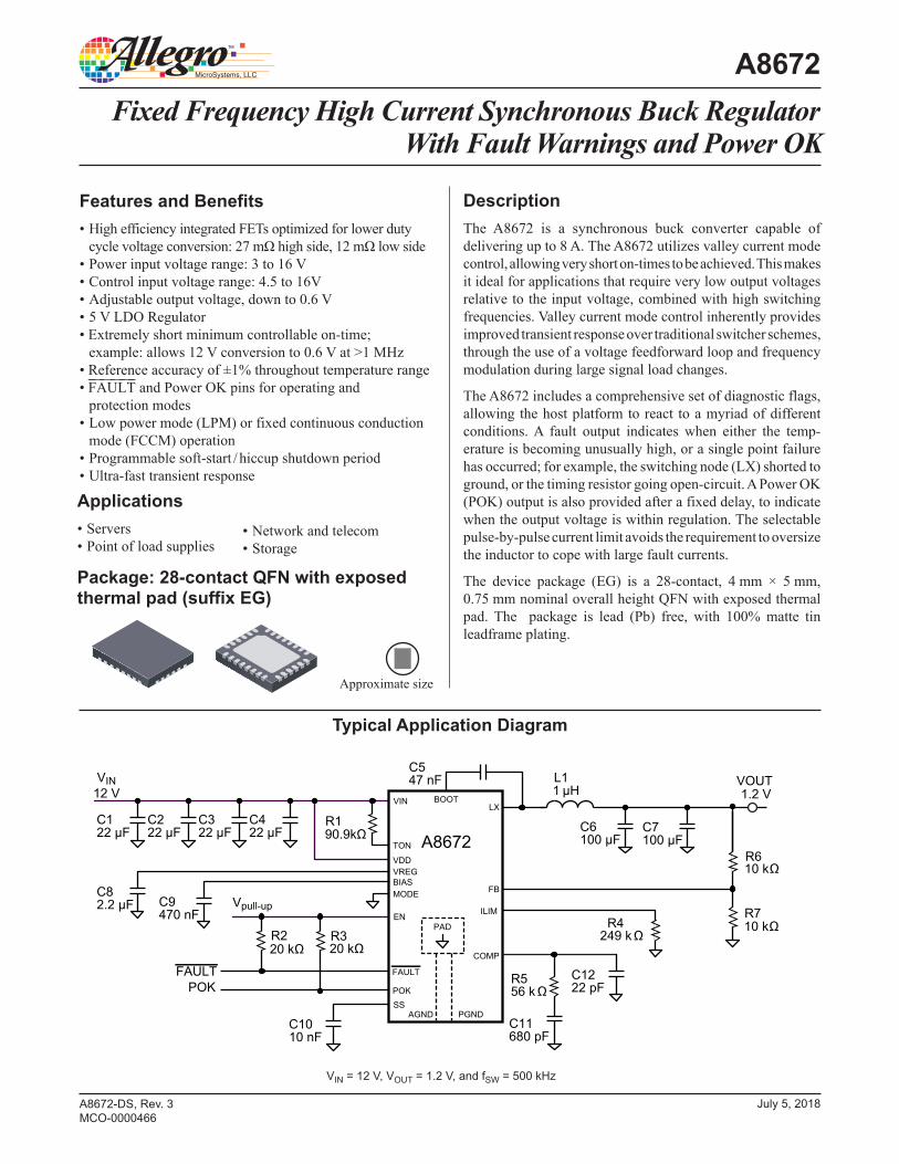
Typical Application Diagram
VIN = 12 V, VOUT = 1.2 V, and fSW = 500 kHz
A8672
Approximate size
VIN 12 V BOOTVIN
TON
VDDVREGBIASMODE
LXC422 µF
C547 nF
SS
VOUT 1.2 V
R7
L11 µH
R190.9kΩ A8672
EN
POKFAULT
Vpull-up
AGND PGND
POK
FAULT
R610 kΩ
10 kΩR3 20 kΩ
R2 20 kΩ
R556 kΩ
R4249 kΩ
COMP
FB
ILIM
C322 µF
C7
100 µF
C6100 µF
C1222 pF
C11680 pF
C222 µF
C122 µF
C82.2 µF C9
470 nF
C1010 nF
PAD
•Networkandtelecom•Storage
July 5, 2018
Fixed Frequency High Current Synchronous Buck Regulator With Fault Warnings and Power OKA8672
2Allegro MicroSystems, LLC 955 Perimeter Road Manchester, NH 03103-3353 U.S.A.www.allegromicro.com
Absolute Maximum RatingsCharacteristic Symbol Notes Rating Unit
VIN, VDD, TON, VREG, BIAS and EN Pin Voltage VI With respect to GND –0.3 to 18 V
LX Pin Voltage VLXWith respect to GND –0.6 to VIN + 0.3 V
t < 50 ns, with respect to GND –2.0 V
BOOT Pin Voltage VBOOT With respect to GND VLX – 0.3 to VLX + 8.0 V
All Other Pins – –0.3 to 7.0 V
Operating Ambient Temperature TA E temperature range –40 to 85 ºC
Maximum Junction Temperature TJ(max) 150 ºC
Storage Temperature Tstg –55 to 150 ºC
Selection GuidePart Number Packing*
A8672EEGTR-T 7000 pieces per 13-inch reel*Contact Allegro™ for additional packing options
Table of Contents
Specifications 2Thermal Characteristics 3Functional Block Diagram 3Pin-out Diagram and Terminal List 4Electrical Characteristics 5
Functional Description 7Basic Operation 7Output Voltage Selection 7Switch On-Time and Switching Frequency 7Valley Current Limit 8Inductor Selection 8
Output Capacitor Selection 9Input Capacitor Selection 9Soft-Start and Output Overloads 10Fault Handling and Reporting 12Control Loop 14Control Loop Design Approach 15Thermal Considerations 18Regulator Efficiency 19
Layout 20Package Outline Drawing 21
Fixed Frequency High Current Synchronous Buck Regulator With Fault Warnings and Power OKA8672
3Allegro MicroSystems, LLC 955 Perimeter Road Manchester, NH 03103-3353 U.S.A.www.allegromicro.com
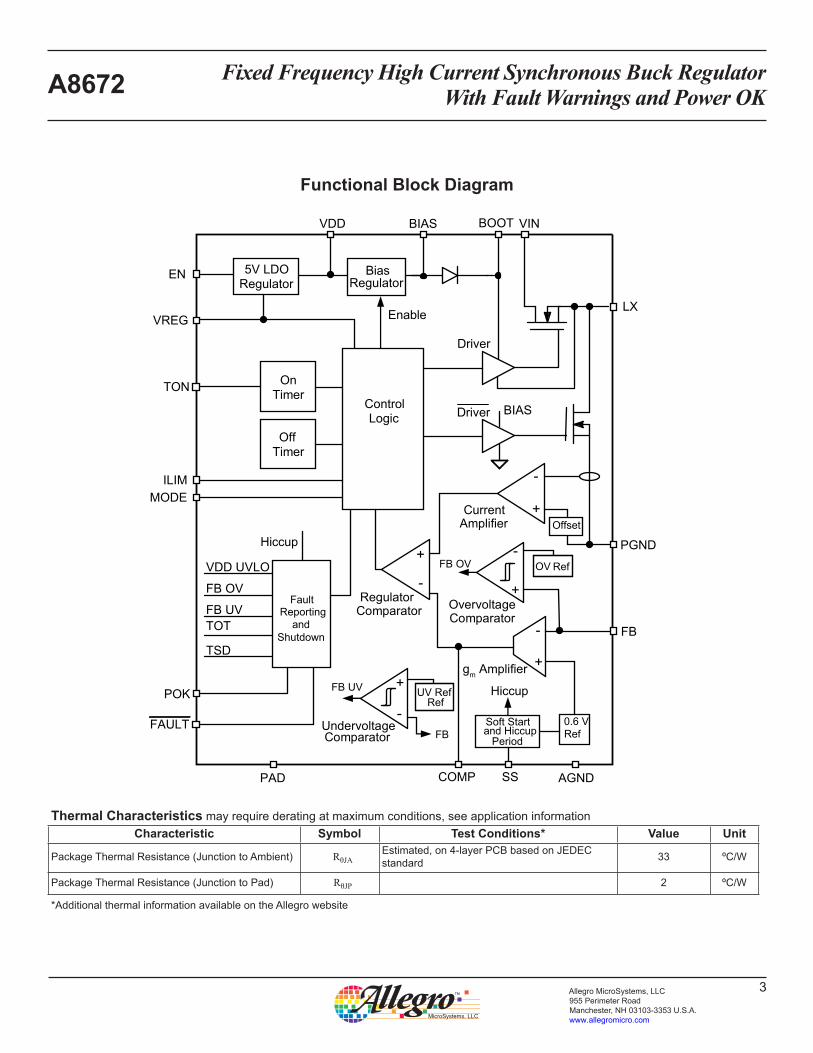
0.6 VRef
+
-
Control Logic
On Timer
Regulator Comparator
OffTimer
Soft Start
Period and Hiccup
Driver
Enable
BiasRegulator
Fault Reporting
and Shutdown
VDD UVLO
TSD
FB OV
VDD VIN
VREG
PGND
AGND
TON
BOOT
SS
EN 5V LDORegulator
+
-
gm Amplifier
BIASDriver
+
-
Current Amplifier
Overvoltage Comparator
Hiccup
Hiccup
OV Ref
FB UV TOT
FB OV
PAD
+
-
COMP
POK FB UV +
-
FB
FB
LX
BIAS
ILIMMODE
Undervoltage Comparator
Offset
UV RefRef
FAULT
Functional Block Diagram
Thermal Characteristics may require derating at maximum conditions, see application informationCharacteristic Symbol Test Conditions* Value Unit
Package Thermal Resistance (Junction to Ambient) RθJAEstimated, on 4-layer PCB based on JEDEC standard 33 ºC/W
Package Thermal Resistance (Junction to Pad) RθJP 2 ºC/W
*Additional thermal information available on the Allegro website
Fixed Frequency High Current Synchronous Buck Regulator With Fault Warnings and Power OKA8672
4Allegro MicroSystems, LLC 955 Perimeter Road Manchester, NH 03103-3353 U.S.A.www.allegromicro.com
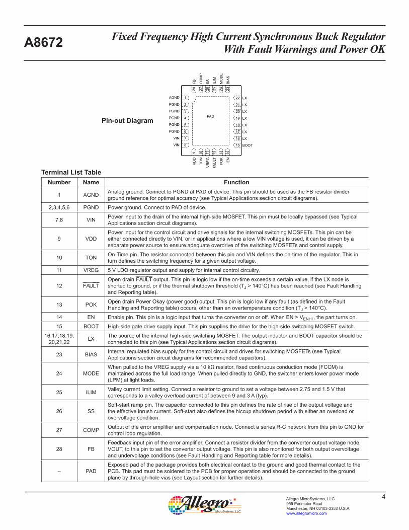
Terminal List TableNumber Name Function
1 AGND Analog ground. Connect to PGND at PAD of device. This pin should be used as the FB resistor divider ground reference for optimal accuracy (see Typical Applications section circuit diagrams).
2,3,4,5,6 PGND Power ground. Connect to PAD of device.
7,8 VIN Power input to the drain of the internal high-side MOSFET. This pin must be locally bypassed (see Typical Applications section circuit diagrams).
9 VDDPower input for the control circuit and drive signals for the internal switching MOSFETs. This pin can be either connected directly to VIN, or in applications where a low VIN voltage is used, it can be driven by a separate power source to ensure adequate overdrive of the switching MOSFETs and control supply.
10 TON On-Time pin. The resistor connected between this pin and VIN defines the on-time of the regulator. This in turn defines the switching frequency for a given output voltage.
11 VREG 5 V LDO regulator output and supply for internal control circuitry.
12 F A U ¯L T Open drain F A U ¯L T output. This pin is logic low if the on-time exceeds a certain value, if the LX node is shorted to ground, or if the thermal shutdown threshold (TJ > 140°C) has been reached (see Fault Handling and Reporting table).
13 POK Open drain Power Okay (power good) output. This pin is logic low if any fault (as defined in the Fault Handling and Reporting table) occurs, other than an overtemperature condition (TJ > 140°C).
14 EN Enable pin. This pin is a logic input that turns the converter on or off. When EN > VENHI , the part turns on.
15 BOOT High-side gate drive supply input. This pin supplies the drive for the high-side switching MOSFET switch.
16,17,18,19, 20,21,22 LX The source of the internal high-side switching MOSFET. The output inductor and BOOT capacitor should be
connected to this pin (see Typical Applications section circuit diagrams).
23 BIAS Internal regulated bias supply for the control circuit and drives for switching MOSFETs (see Typical Applications section circuit diagrams for recommended capacitors).
24 MODEWhen pulled to the VREG supply via a 10 kΩ resistor, fixed continuous conduction mode (FCCM) is maintained across the full load range. When pulled directly to GND, the switcher enters lower power mode (LPM) at light loads.
25 ILIM Valley current limit setting. Connect a resistor to ground to set a voltage between 2.75 and 1.5 V that corresponds to a valley overload current of between 9 and 3 A (typ).
26 SSSoft-start ramp pin. The capacitor connected to this pin defines the rate of rise of the output voltage and the effective inrush current. Soft-start also defines the hiccup shutdown period with either an overload or overvoltage condition.
27 COMP Output of the error amplifier and compensation node. Connect a series R-C network from this pin to GND for control loop regulation.
28 FBFeedback input pin of the error amplifier. Connect a resistor divider from the converter output voltage node, VOUT, to this pin to set the converter output voltage. This pin is also monitored for both output overvoltage and undervoltage conditions (see Fault Handling and Reporting table for more details).
– PADExposed pad of the package provides both electrical contact to the ground and good thermal contact to the PCB. This pad must be soldered to the PCB for proper operation and should be connected to the ground plane by through-hole vias (see Layout section for further details).
Pin-out DiagramPAD
22
21
20
19
18
17
16
15
1
2
3
4
5
6
7
8
9 10 11 12 13 14
28 27 26 25 24 23
FB CO
MP
SS
ILIM
MO
DE
BIA
S
VD
D
TON
VR
EG
FAU
LT
PO
K
EN
LX
LX
LX
LX
LX
LX
LX
BOOT
AGND
PGND
PGND
PGND
PGND
PGND
VIN
VIN
Fixed Frequency High Current Synchronous Buck Regulator With Fault Warnings and Power OKA8672
5Allegro MicroSystems, LLC 955 Perimeter Road Manchester, NH 03103-3353 U.S.A.www.allegromicro.com
Continued on the next page…
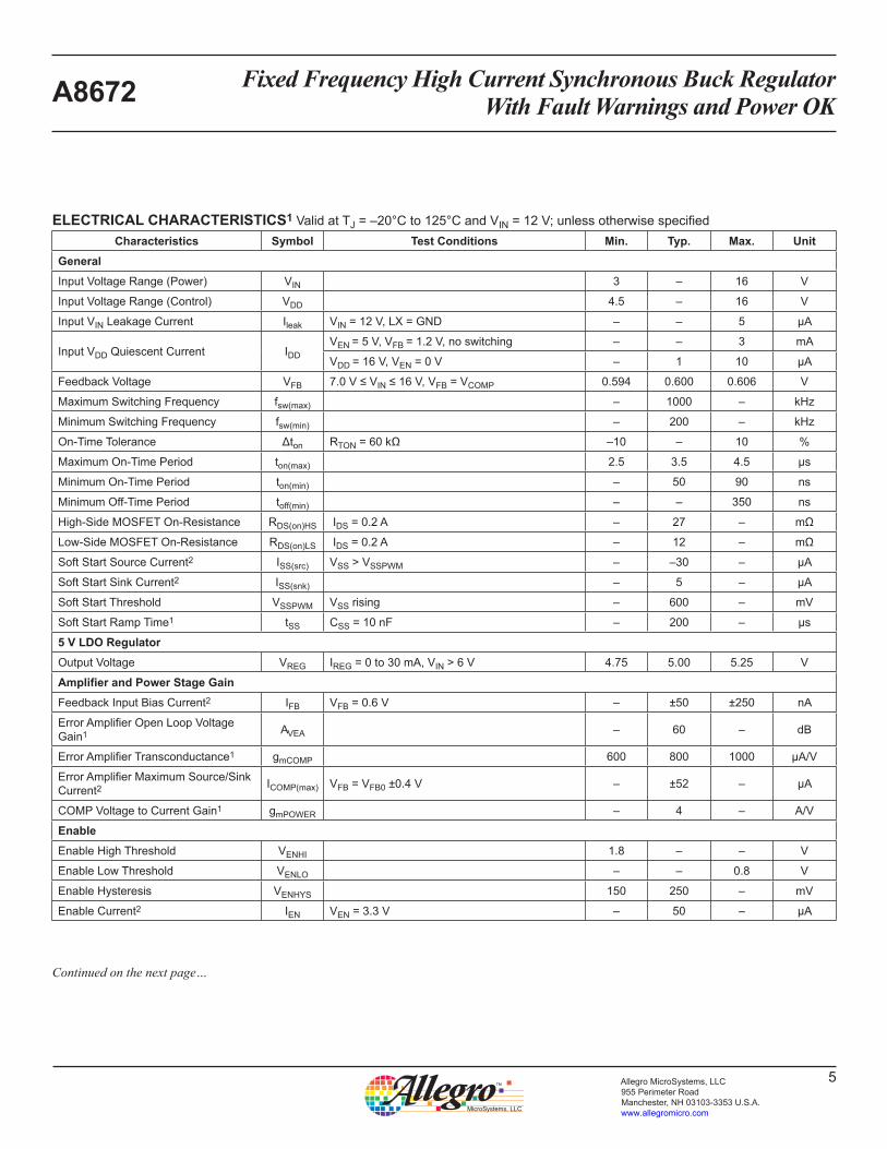
ELECTRICAL CHARACTERISTICS1 Valid at TJ = –20°C to 125°C and VIN = 12 V; unless otherwise specifiedCharacteristics Symbol Test Conditions Min. Typ. Max. Unit
GeneralInput Voltage Range (Power) VIN 3 – 16 V
Input Voltage Range (Control) VDD 4.5 – 16 V
Input VIN Leakage Current Ileak VIN = 12 V, LX = GND – – 5 μA
Input VDD Quiescent Current IDDVEN = 5 V, VFB = 1.2 V, no switching – – 3 mA
VDD = 16 V, VEN = 0 V – 1 10 µA
Feedback Voltage VFB 7.0 V ≤ VIN ≤ 16 V, VFB = VCOMP 0.594 0.600 0.606 V
Maximum Switching Frequency fsw(max) – 1000 – kHz
Minimum Switching Frequency fsw(min) – 200 – kHz
On-Time Tolerance Δton RTON = 60 kΩ –10 – 10 %
Maximum On-Time Period ton(max) 2.5 3.5 4.5 µs
Minimum On-Time Period ton(min) – 50 90 ns
Minimum Off-Time Period toff(min) – – 350 ns
High-Side MOSFET On-Resistance RDS(on)HS IDS = 0.2 A – 27 – mΩ
Low-Side MOSFET On-Resistance RDS(on)LS IDS = 0.2 A – 12 – mΩ
Soft Start Source Current2 ISS(src) VSS > VSSPWM – –30 – µA
Soft Start Sink Current2 ISS(snk) – 5 – µA
Soft Start Threshold VSSPWM VSS rising – 600 – mV
Soft Start Ramp Time1 tSS CSS = 10 nF – 200 – µs
5 V LDO RegulatorOutput Voltage VREG IREG = 0 to 30 mA, VIN > 6 V 4.75 5.00 5.25 V
Amplifier and Power Stage GainFeedback Input Bias Current2 IFB VFB = 0.6 V – ±50 ±250 nA
Error Amplifier Open Loop Voltage Gain1 AVEA – 60 – dB
Error Amplifier Transconductance1 gmCOMP 600 800 1000 µA/V
Error Amplifier Maximum Source/Sink Current2 ICOMP(max) VFB = VFB0 ±0.4 V – ±52 – µA
COMP Voltage to Current Gain1 gmPOWER – 4 – A/V
EnableEnable High Threshold VENHI 1.8 – – V
Enable Low Threshold VENLO – – 0.8 V
Enable Hysteresis VENHYS 150 250 – mV
Enable Current2 IEN VEN = 3.3 V – 50 – µA
Fixed Frequency High Current Synchronous Buck Regulator With Fault Warnings and Power OKA8672
6Allegro MicroSystems, LLC 955 Perimeter Road Manchester, NH 03103-3353 U.S.A.www.allegromicro.com
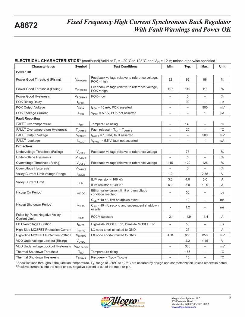
ELECTRICAL CHARACTERISTICS1 (continued) Valid at TJ = –20°C to 125°C and VIN = 12 V; unless otherwise specifiedCharacteristics Symbol Test Conditions Min. Typ. Max. Unit
Power OK
Power Good Threshold (Rising) VPOK(HI)Feedback voltage relative to reference voltage, POK = high 92 95 98 %
Power Good Threshold (Falling) VPOK(LO)Feedback voltage relative to reference voltage, POK = high 107 110 113 %
Power Good Hysteresis VPOKHYS POK= low – 5 – %
POK Rising Delay tdPOK – 90 – µs
POK Output Voltage VPOK IPOK = 10 mA, POK asserted – – 500 mV
POK Leakage Current IPOK VPOK = 5.5 V, POK not asserted – – 1 μA
Fault ReportingF A U ¯L T Overtemperature TOT Temperature rising – 140 – °C
F A U ¯L T Overtemperature Hysteresis TOTHYS Fault release = TOT – TOTHYS – 20 – °C
F A U ¯L T Output Voltage VFAULT IFAULT = 10 mA, fault asserted – – 500 mV
F A U ¯L T Leakage IFAULT VFAULT = 5.5 V, fault not asserted – – 1 µA
ProtectionUndervoltage Threshold (Falling) VUVFB Feedback voltage relative to reference voltage – 75 – %
Undervoltage Hysteresis VUVHYS – 5 – %
Overvoltage Threshold (Rising) VOVFB Feedback voltage relative to reference voltage 115 120 125 %
Overvoltage Hysteresis VOVHYS – 5 – %
Valley Current Limit Voltage Range ILIMVR 1.0 – 2.75 V
Valley Current Limit ILIMILIM resistor = 169 kΩ 3.0 4.0 5.0 A
ILIM resistor = 249 kΩ 6.0 8.0 10.0 A
Hiccup On Period1 tHICOCEither valley current limit or overvoltage condition reached – 50 – µs
Hiccup Shutdown Period1 tHICSD
CSS = 10 nF, first shutdown event – 10 – ms
CSS = 10 nF, second and subsequent shutdown events - 1.2 - ms
Pulse-by-Pulse Negative Valley Current Limit INLIM FCCM selected –2.4 –1.9 –1.4 A
FB Overvoltage Duration tUVFB High-side MOSFET off, low-side MOSFET on – 50 – μs
High-Side MOSFET Protection Current IHIPRO LX node short-circuited to GND – 25 – A
High-Side MOSFET Protection Voltage VHIPRO LX node short-circuited to GND 450 650 850 mV
VDD Undervoltage Lockout (Rising) VUVLO – 4.2 4.45 V
VDD Undervoltage Lockout Hysteresis VUVLOHYS – 300 – mV
Thermal Shutdown Threshold TSD Temperature rising – 165 – °C
Thermal Shutdown Hysteresis TSDHYS Recovery = TSD – TSDHYS – 15 – °C1Specifications throughout the junction temperature, TJ , range of –20ºC to 125ºC are assured by design and characterization unless otherwise noted.2Positive current is into the node or pin, negative current is out of the node or pin.
Fixed Frequency High Current Synchronous Buck Regulator With Fault Warnings and Power OKA8672
7Allegro MicroSystems, LLC 955 Perimeter Road Manchester, NH 03103-3353 U.S.A.www.allegromicro.com
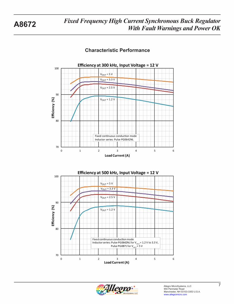
Characteristic Performance
70
80
90
100
0 1 2 3 4 5 6
Effici
ency
(%
)
Load Current (A)
Efficiency at 300 kHz, Input Voltage = 12 V
VOUT = 5 V
VOUT = 3.3 V
VOUT = 2.5 V
VOUT = 1.2 V
Fixed continuous conduction mode Inductor series: Pulse PG0642NL
70
80
90
100
0 1 2 3 4 5 6
Effici
ency
(%
)
Load Current (A)
Efficiency at 500 kHz, Input Voltage = 12 V
VOUT = 5 V
VOUT = 3.3 V
VOUT = 2.5 V
VOUT = 1.2 V
Fixed continuous conduction mode Inductor series: Pulse PG0642NL for VOUT = 1.2 V to 3.3 V, Pulse PG0871 for VOUT = 5 V
Fixed Frequency High Current Synchronous Buck Regulator With Fault Warnings and Power OKA8672
8Allegro MicroSystems, LLC 955 Perimeter Road Manchester, NH 03103-3353 U.S.A.www.allegromicro.com
Functional Description
Basic OperationAt the beginning of a switching cycle, the high-side switch is turned on for a duration determined by the current flowing into TON. The magnitude of current is determined by the value of the inputvoltageandthevalueoftheon-timeresistor(RTON,R1inthe Typical Applications section circuit diagrams).
Duringtheon-timeperiod,thecurrentbuildsupthroughtheinductor at a rate determined by the voltage developed across it and the inductance value. When the on-time period elapses, the outputofanRSlatchresets,turningoffthehigh-sideswitch.After a small dead-time delay, the low-side switch is turned on.
The current through the inductor decays at a rate determined by the output voltage and the inductance value. The current is sensed through the low-side switch and is compared to the cur-rent demand signal. The current demand signal is generated by comparing the output voltage (stepped down to the FB pin) with an accurate reference voltage.
When the current through the low-side switch drops to the current demand level, the low-side switch is turned off. After a further dead-time delay, the high-side switch is turned on again, and the process is repeated.
Output Voltage Selection The output voltage (VOUT) of the converter is set by selecting the appropriate feedback resistors using the following formula:
VOUT VFB IFB1+ +=R6R7
R6 R7R6 + R7
(1)
where:
VFB is the reference voltage,
R6andR7areasshownintheTypicalApplicationssectioncircuit diagrams, and
IFB is the reference bias current.
It is important to consider the tolerance of the feedback resistors, because they directly affect the overall setpoint accuracy of the output voltage.
It is also important to consider the actual resistor values selected andconsiderthetrade-offs.Highvalueresistorswillminimizethe shunt current flowing through the feedback network, enhanc-ingefficiency.However,theoffseterrorproducedbytherefer-
ence bias current will increase, affecting the regulation. In addi-tion, high value resistors are more prone to noise pick-up effects which may affect performance. As some kind of compromise, it isrecommendedthatR7beintheregionof10kΩ.
Switch On-Time and Switching Frequency The switching frequency of the converter is selected by choosing the appropriate on-time. The on-time can be estimated to a first order by using the following formula:
tonVOUT 1VIN
= fSW (2)
where:
VOUT is the output voltage,
fSW is the switching frequency, and
VIN is the nominal input voltage.
To factor-in the effects of resistive voltage drops in the converter circuit, the following formula can be used to produce a more accurate estimate of what the on-time has to be for a required switching frequency:
tonVOUT + (RDS(on)LS + DCRL ) VIN + (RDS(on)LS – RDS(on)HS )
IOUT 1= IOUT fSW (3)
where:
RDS(on)LSisthelow-sideMOSFETon-resistance,
RDS(on)HSisthehigh-sideMOSFETresistance,and
DCRL is the inductive resistance.
The switching frequency will vary slightly as the resistive voltage drops in the circuit change, either due to temperature effects or to input voltage variations.
Note that when selecting the switching frequency, care should be taken to ensure the converter does not operate near either the minimum on-time (50 ns) or the minimum off-time (250 ns). Minimum on-times will typically occur in combinations of maximum input voltage, minimum output voltage with minimum load, and maximum switching frequency. Minimum off-times will typically occur in combinations of minimum input voltage, maximum output voltage with maximum load, and maximum switching frequency.
Fixed Frequency High Current Synchronous Buck Regulator With Fault Warnings and Power OKA8672
9Allegro MicroSystems, LLC 955 Perimeter Road Manchester, NH 03103-3353 U.S.A.www.allegromicro.com
The ton from either of the above formulae can be used to deter-minetheTONresistorvalue,RTON(R1inTypicalApplicationssection circuit drawings):
RTONton – 8 ×10⁻⁹
25 ×10–12 (VIN – 0.67) – 500=
(4)
Table 1 provides preferred resistor values for a given output voltageattargetswitchingfrequenciesof500kHz,700kHz,and1MHz:
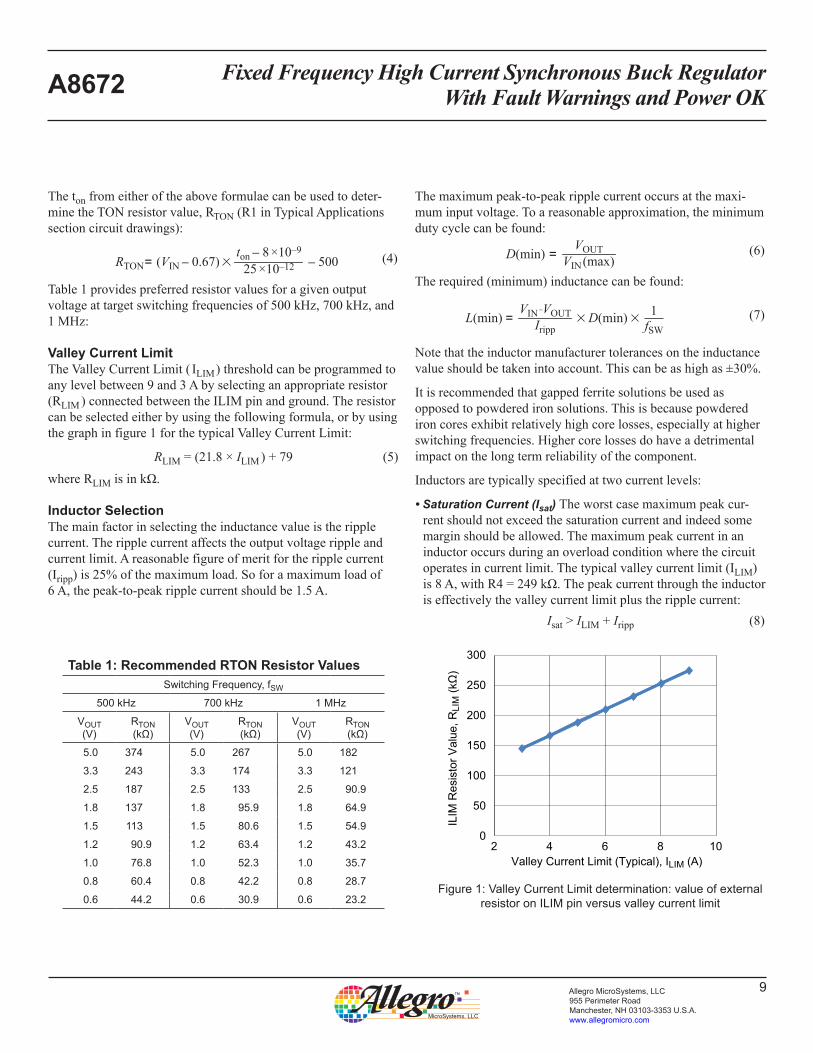
Valley Current Limit TheValleyCurrentLimit(ILIM ) threshold can be programmed to anylevelbetween9and3Abyselectinganappropriateresistor(RLIM ) connected between the ILIM pin and ground. The resistor can be selected either by using the following formula, or by using thegraphinfigure1forthetypicalValleyCurrentLimit:
RLIM = (21.8 × ILIM ) + 79 (5)whereRLIMisinkΩ.
Inductor Selection The main factor in selecting the inductance value is the ripple current. The ripple current affects the output voltage ripple and current limit. A reasonable figure of merit for the ripple current (Iripp)is25%ofthemaximumload.Soforamaximumloadof6 A, the peak-to-peak ripple current should be 1.5 A.
The maximum peak-to-peak ripple current occurs at the maxi-mum input voltage. To a reasonable approximation, the minimum duty cycle can be found:
D(min)VOUT
VIN (max)=
(6)
The required (minimum) inductance can be found:
L(min) D(min)VIN –VOUT
Iripp= 1
fSW (7)
Note that the inductor manufacturer tolerances on the inductance valueshouldbetakenintoaccount.Thiscanbeashighas±30%.
It is recommended that gapped ferrite solutions be used as opposed to powdered iron solutions. This is because powdered iron cores exhibit relatively high core losses, especially at higher switchingfrequencies.Highercorelossesdohaveadetrimentalimpact on the long term reliability of the component.
Inductors are typically specified at two current levels:
• Saturation Current (Isat) The worst case maximum peak cur-rent should not exceed the saturation current and indeed some margin should be allowed. The maximum peak current in an inductor occurs during an overload condition where the circuit operates in current limit. The typical valley current limit (ILIM) is8A,withR4=249kΩ.Thepeakcurrentthroughtheinductoris effectively the valley current limit plus the ripple current:
Isat > ILIM + Iripp (8)
ILIM
Res
isto
r Val
ue, R
LIM
(kΩ
)
2 4 6 8 10
300
250
200
150
100
50
0
Valley Current Limit (Typical), ILIM (A)
Figure 1: Valley Current Limit determination: value of external resistor on ILIM pin versus valley current limit
Table 1: Recommended RTON Resistor ValuesSwitching Frequency, fSW
500 kHz 700 kHz 1 MHz
VOUT (V)
RTON (kΩ)
VOUT (V)
RTON (kΩ)
VOUT (V)
RTON (kΩ)
5.0 374 5.0 267 5.0 182
3.3 243 3.3 174 3.3 121
2.5 187 2.5 133 2.5 90.9
1.8 137 1.8 95.9 1.8 64.9
1.5 113 1.5 80.6 1.5 54.9
1.2 90.9 1.2 63.4 1.2 43.2
1.0 76.8 1.0 52.3 1.0 35.7
0.8 60.4 0.8 42.2 0.8 28.7
0.6 44.2 0.6 30.9 0.6 23.2
Fixed Frequency High Current Synchronous Buck Regulator With Fault Warnings and Power OKA8672
10Allegro MicroSystems, LLC 955 Perimeter Road Manchester, NH 03103-3353 U.S.A.www.allegromicro.com
•Rms Current (Irms) It is important to understand how the rms currentlevelisspecifiedintermsofambienttemperature.Somemanufacturers quote an ambient whilst others quote a tempera-ture that includes a self-temperature rise. For example, if an inductorisratedfor85°Candincludesaself-temperatureriseof25°Catmaximumload,thentheinductorcannotbesafelyoper-atedbeyondanambienttemperatureof60°Catfullload. The rms current through the inductor should not exceed the rat-ing for the inductor, taking into account the maximum ambient temperature. The maximum rms current is effectively the valley current limit (ILIM) plus half of the ripple current:
Irms(max) > ILIM + Iripp/2 (9)
A final consideration in the selection of the inductor is the series resistance(DCR).AlowerDCRwillreducethepowerlossandenhance power efficiency. The trade-off in using an inductor with arelativelylowDCRisthephysicalsizeistypicallylarger.
Recommendedinductor:PIMC065T-XXMN-11 (XX is value) seriesmanufacturedbyCyntecorthePG0871seriesmanufac-tured by Pulse Electronics. Table 2 provides preferred inductor values for a given output voltage, 2 A output at target switching frequenciesof500kHz,700kHz,and1MHz.
Output Capacitor SelectionThe output capacitor has two main functions: influence the con-trolloopresponse(seetheControlLoopsection),anddeterminethe magnitude of the output voltage ripple.
The output voltage ripple can be approximated to:
VrippIripp
COUTfSW8= (10)
where:
Iripp is the peak-to-peak current in the inductor (see the Inductor Selectionsection),and
COUT is the output capacitance.
It is recommended that ceramic capacitors be used, taking into account: size, cost, reliability, and performance. It is imperative thatceramictypeX5RorX7Rareused.OnnoaccountshouldY5V, Y5U, Z5U, or similar be used, because the capacitance tolerance and the temperature stability is very poor.
There is generally no need to consider the effects of heating caused by the ripple current flowing into the output capacitor. Thisisbecausetheequivalentseriesresistance(ESR)ofceramiccapacitors is extremely low.
When using ceramic capacitors, it is important to consider the effects of capacitance reduction due to the E-field. To avoid this voltage bias effect, it is recommended that the capacitor rated voltagebeatleasttwicethatoftheactualoutputvoltage.Soforexample, with a 5 V output, the capacitor should be rated to 10 V.
Forthemajorityofapplications,acapacitanceof200µFisrec-ommended to ensure good transient response.
Input Capacitor SelectionThe function of the input capacitor is to provide a low impedance shunt path for the current drawn by the A8672 when the high-side switch is on. This minimizes the amount of ripple current reflected back into the source supply. This reduces the potential for higher conducted electromagnetic interference (EMI).
In a correctly designed system, with a quality capacitor posi-tionedadjacenttotheVINpinandthePGNDpin,thiscapacitorshould supply the high-side switch current minus the average inputcurrent.Duringthehigh-sideswitchoff-cycle,thecapacitoris charged by the average input current.
Table 2: Recommended Inductor ValuesSwitching Frequency, fSW
500 kHz 700 kHz 1 MHz
VOUT (V)
L (µH)
VOUT (V)
L (µH)
VOUT (V)
L (µH)
5.0 3.7 5.0 2.6 5.0 2.2
3.3 3.7 3.3 2.2 3.3 1.7
2.5 2.6 2.5 1.7 2.5 1.2
1.8 2.2 1.8 1.7 1.8 1
1.5 1.7 1.5 1.2 1.5 1
1.2 1.2 1.2 1 1.2 0.8
1.0 1.2 1.0 1 1.0 0.54
0.8 1 0.8 0.8 0.8 0.47
0.6 0.8 0.6 0.47 0.6 0.47
Fixed Frequency High Current Synchronous Buck Regulator With Fault Warnings and Power OKA8672
11Allegro MicroSystems, LLC 955 Perimeter Road Manchester, NH 03103-3353 U.S.A.www.allegromicro.com
The effective rms current that flows in the input filter capaci-tor is:
IrmsVOUT
VOUT
IOUTVIN
VIN – 11/2
=
(11)
The amount of ripple voltage (Vripp ) that appears across the inputterminals(VINwithrespecttoGND)isdeterminedbytheamount of charge removed from the input capacitor during the high-side switch conduction time. If a capacitor technology such asanelectrolyticisused,thentheeffectsoftheESRshouldalsobe taken into account.
Theamountofinputcapacitance(CIN) required for a given ripple voltage can be found:
CINIrms ton
Vripp=
(12)
where:
tonistheon-timeofthehigh-sideswitch(seetheSwitchOn-TimeandSwitchingFrequencysection;notethatmaximumtonoccurs at minimum input voltage), and
CINistheinputfiltercapacitance.
AsmentionedintheOutputCapacitorSelectionsection,theeffects of voltage biasing should be taken into account when choosing the capacitor voltage rating. If ceramic capacitors are being used, then there is generally no need to consider the effects ofESRheating.
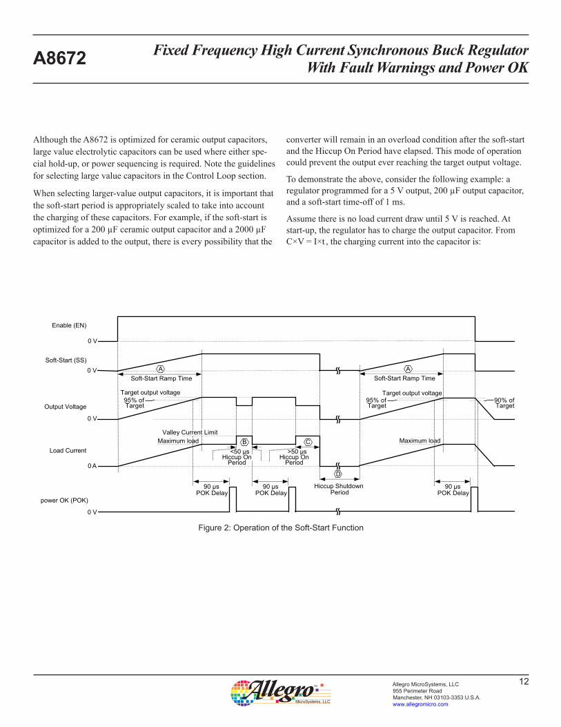
Soft-Start, Output Overloads and OvervoltagesThe soft-start routine controls the rate of rise of the reference voltage, which in turn controls the FB pin, and thereby the out-put voltage (VOUT )(see figure 2). This function minimizes the amount of inrush current drawn from the input voltage (VIN ) and potential voltage overshoot on the output rail (VOUT ).
A soft-start routine is initiated when the enable pin (EN) is high, no overvoltage exists on the output, the thermal protec-tion circuitry is not activated, and VIN is above the undervoltage threshold. Immediately after EN goes high, the soft-start capaci-torischargedviaaninternal10µAsourceandPWMswitchingaction occurs.
TheSoft-StartRampTime,tss , can be found from the following formula:
tSSCSS 0.630 ×10 –6=
(13)
whereCSSisC11intheTypicalApplicationcircuitdiagrams.
DuringtheSoft-Start Ramp Time (see A in figure 2), the refer-ence is ramped from 0 up to 0.6 V, and the output voltage ( VOUT ) tracks the reference voltage. The POK flag is held low until the output voltage reaches 95% (typical) of the target voltage and a delayof90µs(typical)occurs.
When an output overcurrent event occurs, the regulator imme-diately limits the valley current at a constant level on a pulse-by pulse basis. The output voltage will tend to fold back, depending on how low the output impedance is. When the output voltage drops below 90% (typical) of the target voltage, the POK flag goes low. If the overload occurs for shorter than the Hiccup On Period(<50µs;Binfigure2),theoutputwillautomaticallyrecover to the target level. If the overload occurs for longer than theHiccupOnPeriod(>50µs;Cinfigure2),theregulatorwill shut down, the soft-start capacitor will be discharged, and (assuming no other fault conditions exist and the enable pin is still high) the regulator will be delayed by the Hiccup Shutdown Period(Dinfigure2).
TheHiccupShutdownPeriodensuresthatprolongedoverloadconditionsdonotcauseexcessivejunctiontemperaturestooccur.AftertheHiccupShutdownPeriodhaselapsed,theoutputvolt-age is again brought up, controlled by the soft-start function. However,iftheoverloadconditionstillexistsandstillremainsaftertheSoft-StartRampTimehaselapsed,theregulatorwillshut down and the process will repeat until the fault is removed.
TheHiccupShutdownPeriodisdeterminedbythedischargeofthesoft-startcapacitortozerovoltage.Duringnormaloperation,thesoft-startcapacitorCSS is charged to 5 V. In the event of an overloadwheretheHiccupOnPeriodexceeds50µs,thelengthofthefirstHiccupShutdownPeriodeventcanbefound:
tSS(first)=(CSS ×5)/5× 10–6 (14)
Soforexample,withaCSSof10nF,thefirstHiccupShutdownPeriod event is 10 ms.
Assuming the overload is still applied, the length of the second andsubsequentHiccupShutdownPeriodsdependsontheloadresistance applied and how far the soft-start capacitor is charged beforeswitchingactionoccurs.TheHiccupShutdownPeriodisapproximately ten times the length of the switching period.
The overvoltage protection operates in a similar way to the over-currentprotectionusingthesameHiccupCircuitry.
Fixed Frequency High Current Synchronous Buck Regulator With Fault Warnings and Power OKA8672
12Allegro MicroSystems, LLC 955 Perimeter Road Manchester, NH 03103-3353 U.S.A.www.allegromicro.com
Figure 2: Operation of the Soft-Start Function
Enable (EN)
Soft-Start (SS)
Output Voltage
Load Current
0 V
0 V
power OK (POK)
0 V
0 A
0 VSoft-Start Ramp Time
<50 µs
90 µsPOK Delay
90 µsPOK Delay
90 µsPOK Delay
Valley Current LimitMaximum load
>50 µs Hiccup On
PeriodHiccup On
Period
Target output voltage95% of Target
Soft-Start Ramp Time
Maximum load
Target output voltage
Hiccup Shutdown Period
A A
B C
D
95% of Target
90% of Target
Although the A8672 is optimized for ceramic output capacitors, large value electrolytic capacitors can be used where either spe-cial hold-up, or power sequencing is required. Note the guidelines forselectinglargevaluecapacitorsintheControlLoopsection.
When selecting larger-value output capacitors, it is important that the soft-start period is appropriately scaled to take into account the charging of these capacitors. For example, if the soft-start is optimizedfora200µFceramicoutputcapacitoranda2000µFcapacitor is added to the output, there is every possibility that the
converter will remain in an overload condition after the soft-start andtheHiccupOnPeriodhaveelapsed.Thismodeofoperationcould prevent the output ever reaching the target output voltage.
To demonstrate the above, consider the following example: a regulatorprogrammedfora5Voutput,200µFoutputcapacitor,and a soft-start time-off of 1 ms.
Assume there is no load current draw until 5 V is reached. At start-up, the regulator has to charge the output capacitor. From C×V=I×t,thechargingcurrentintothecapacitoris:
Fixed Frequency High Current Synchronous Buck Regulator With Fault Warnings and Power OKA8672
13Allegro MicroSystems, LLC 955 Perimeter Road Manchester, NH 03103-3353 U.S.A.www.allegromicro.com
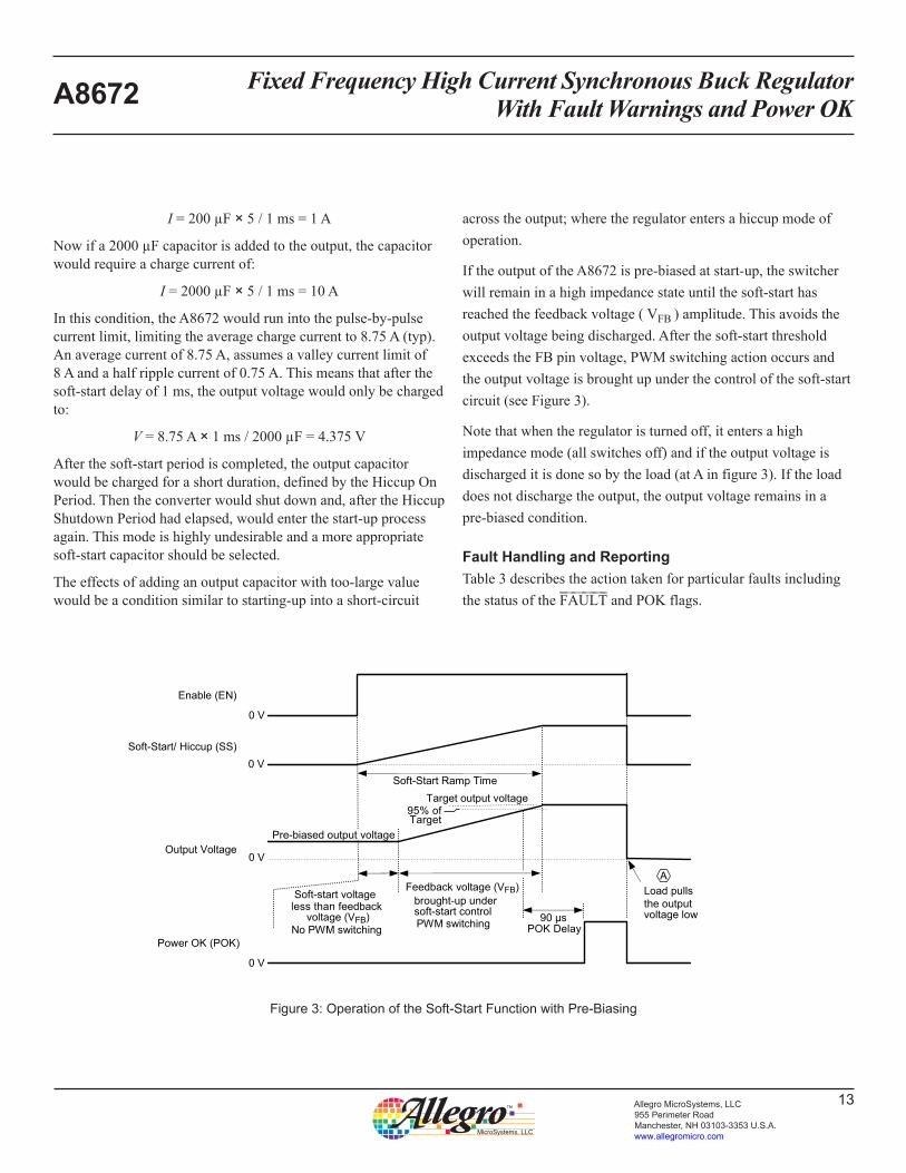
I=200µF×5/1ms=1A
Nowifa2000µFcapacitorisaddedtotheoutput,thecapacitorwould require a charge current of:
I=2000µF×5/1ms=10A
In this condition, the A8672 would run into the pulse-by-pulse current limit, limiting the average charge current to 8.75 A (typ). An average current of 8.75 A, assumes a valley current limit of 8 A and a half ripple current of 0.75 A. This means that after the soft-start delay of 1 ms, the output voltage would only be charged to:
V = 8.75 A ×1ms/2000µF=4.375V
After the soft-start period is completed, the output capacitor wouldbechargedforashortduration,definedbytheHiccupOnPeriod.Thentheconverterwouldshutdownand,aftertheHiccupShutdownPeriodhadelapsed,wouldenterthestart-upprocessagain. This mode is highly undesirable and a more appropriate soft-start capacitor should be selected.
The effects of adding an output capacitor with too-large value would be a condition similar to starting-up into a short-circuit
across the output; where the regulator enters a hiccup mode of operation.
If the output of the A8672 is pre-biased at start-up, the switcher will remain in a high impedance state until the soft-start has reached the feedback voltage ( VFB ) amplitude. This avoids the output voltage being discharged. After the soft-start threshold exceeds the FB pin voltage, PWM switching action occurs and the output voltage is brought up under the control of the soft-start circuit(seeFigure3).
Note that when the regulator is turned off, it enters a high impedance mode (all switches off) and if the output voltage is dischargeditisdonesobytheload(atAinfigure3).Iftheloaddoes not discharge the output, the output voltage remains in a pre-biased condition.
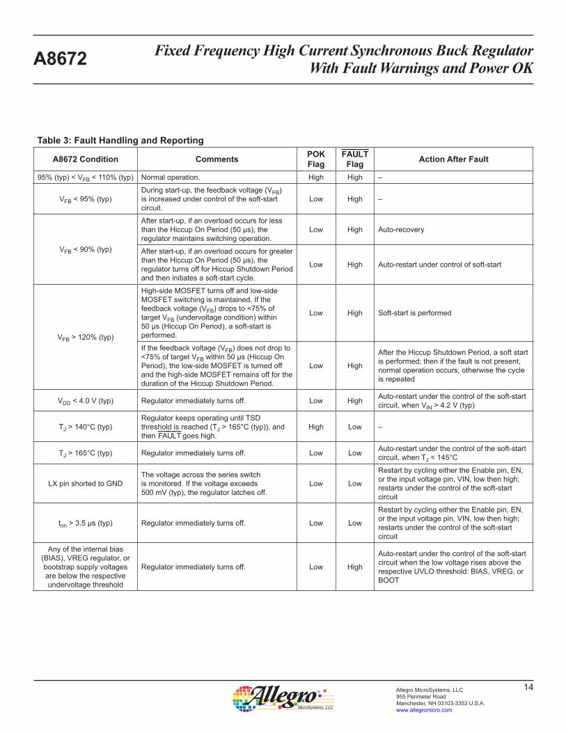
Fault Handling and ReportingTable3describestheactiontakenforparticularfaultsincludingthe status of the F A U L T and POK flags.
95% of Target
90 µsPOK Delay
Soft-start voltage less than feedback
voltage (VFB)No PWM switching
Enable (EN)
Soft-Start/ Hiccup (SS)
Output Voltage
0 V
Power OK (POK)
0 V
0 V
0 VSoft-Start Ramp Time
Target output voltage
Pre-biased output voltage
Feedback voltage (VFB) brought-up under
soft-start control PWM switching
Load pulls the output voltage low
A
Figure 3: Operation of the Soft-Start Function with Pre-Biasing
Fixed Frequency High Current Synchronous Buck Regulator With Fault Warnings and Power OKA8672
14Allegro MicroSystems, LLC 955 Perimeter Road Manchester, NH 03103-3353 U.S.A.www.allegromicro.com
Table 3: Fault Handling and Reporting
A8672 Condition Comments POK Flag
F AU ¯L T Flag Action After Fault
95% (typ) < VFB < 110% (typ) Normal operation. High High –
VFB < 95% (typ)During start-up, the feedback voltage (VFB) is increased under control of the soft-start circuit.
Low High –
VFB < 90% (typ)
After start-up, if an overload occurs for less than the Hiccup On Period (50 μs), the regulator maintains switching operation.
Low High Auto-recovery
After start-up, if an overload occurs for greater than the Hiccup On Period (50 μs), the regulator turns off for Hiccup Shutdown Period and then initiates a soft-start cycle.
Low High Auto-restart under control of soft-start
VFB > 120% (typ)
High-side MOSFET turns off and low-side MOSFET switching is maintained. If the feedback voltage (VFB) drops to <75% of target VFB (undervoltage condition) within 50 μs (Hiccup On Period), a soft-start is performed.
Low High Soft-start is performed
If the feedback voltage (VFB) does not drop to <75% of target VFB within 50 μs (Hiccup On Period), the low-side MOSFET is turned off and the high-side MOSFET remains off for the duration of the Hiccup Shutdown Period.
Low High
After the Hiccup Shutdown Period, a soft start is performed; then if the fault is not present, normal operation occurs, otherwise the cycle is repeated
VDD < 4.0 V (typ) Regulator immediately turns off. Low High Auto-restart under the control of the soft-start circuit, when VIN > 4.2 V (typ)
TJ > 140°C (typ)Regulator keeps operating until TSD threshold is reached (TJ > 165°C (typ)), and then F AU ¯L T goes high.
High Low –
TJ > 165°C (typ) Regulator immediately turns off. Low Low Auto-restart under the control of the soft-start circuit, when TJ < 145°C
LX pin shorted to GNDThe voltage across the series switch is monitored. If the voltage exceeds 500 mV (typ), the regulator latches off.
Low Low
Restart by cycling either the Enable pin, EN, or the input voltage pin, VIN, low then high; restarts under the control of the soft-start circuit
ton > 3.5 μs (typ) Regulator immediately turns off. Low Low
Restart by cycling either the Enable pin, EN, or the input voltage pin, VIN, low then high; restarts under the control of the soft-start circuit
Any of the internal bias (BIAS), VREG regulator, or bootstrap supply voltages are below the respective undervoltage threshold
Regulator immediately turns off. Low High
Auto-restart under the control of the soft-start circuit when the low voltage rises above the respective UVLO threshold: BIAS, VREG, or BOOT
Fixed Frequency High Current Synchronous Buck Regulator With Fault Warnings and Power OKA8672
15Allegro MicroSystems, LLC 955 Perimeter Road Manchester, NH 03103-3353 U.S.A.www.allegromicro.com
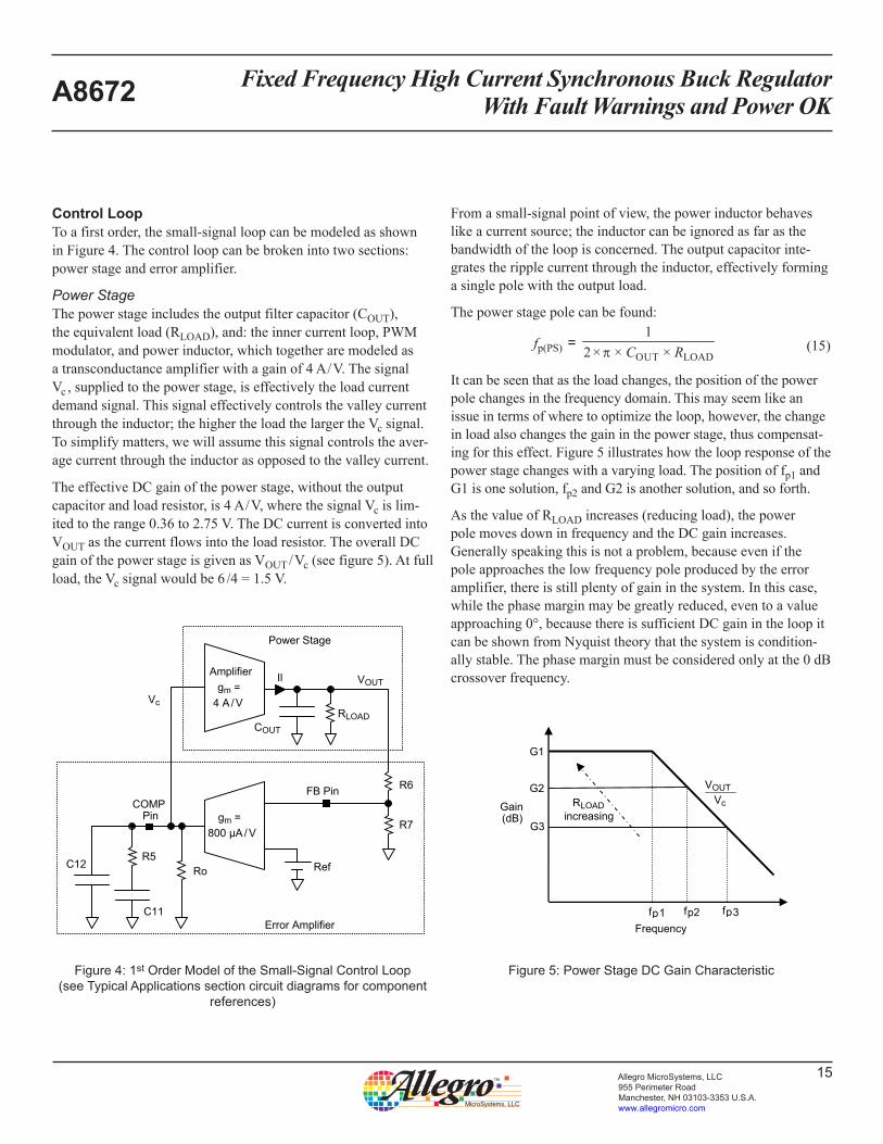
Control LoopTo a first order, the small-signal loop can be modeled as shown in Figure 4. The control loop can be broken into two sections: power stage and error amplifier.
Power StageThepowerstageincludestheoutputfiltercapacitor(COUT), theequivalentload(RLOAD), and: the inner current loop, PWM modulator, and power inductor, which together are modeled as atransconductanceamplifierwithagainof4A/V.ThesignalVc , supplied to the power stage, is effectively the load current demand signal. This signal effectively controls the valley current through the inductor; the higher the load the larger the Vc signal. To simplify matters, we will assume this signal controls the aver-age current through the inductor as opposed to the valley current.
TheeffectiveDCgainofthepowerstage,withouttheoutputcapacitorandloadresistor,is4A/V,wherethesignalVc is lim-itedtotherange0.36to2.75V.TheDCcurrentisconvertedintoVOUTasthecurrentflowsintotheloadresistor.TheoverallDCgain of the power stage is given as VOUT/Vc (see figure 5). At full load, the Vcsignalwouldbe6/ 4 = 1.5 V.
From a small-signal point of view, the power inductor behaves like a current source; the inductor can be ignored as far as the bandwidth of the loop is concerned. The output capacitor inte-grates the ripple current through the inductor, effectively forming a single pole with the output load.
The power stage pole can be found:
fp(PS)1
= 2 × × COUT × RLOAD (15)
It can be seen that as the load changes, the position of the power pole changes in the frequency domain. This may seem like an issue in terms of where to optimize the loop, however, the change in load also changes the gain in the power stage, thus compensat-ing for this effect. Figure 5 illustrates how the loop response of the power stage changes with a varying load. The position of fp1 and G1 is one solution, fp2 and G2 is another solution, and so forth.
AsthevalueofRLOAD increases (reducing load), the power polemovesdowninfrequencyandtheDCgainincreases.Generally speaking this is not a problem, because even if the pole approaches the low frequency pole produced by the error amplifier, there is still plenty of gain in the system. In this case, while the phase margin may be greatly reduced, even to a value approaching0°,becausethereissufficientDCgainintheloopitcan be shown from Nyquist theory that the system is condition-ally stable. The phase margin must be considered only at the 0 dB crossover frequency.
Figure 4: 1st Order Model of the Small-Signal Control Loop(see Typical Applications section circuit diagrams for component
references)
Figure 5: Power Stage DC Gain Characteristic
COUT
RLOAD
R6
R7
COMPPin
C11
C12R5
FB Pin
Vc
Il
Power Stage
VOUT
Error Amplifier
Amplifier gm =
4 A / V
gm = 800 µA / V
RefRo
Vc
VOUT
RLOAD increasing
Gain (dB)
G1
G3
G2
fp1 fp2 fp3Frequency
Fixed Frequency High Current Synchronous Buck Regulator With Fault Warnings and Power OKA8672
16Allegro MicroSystems, LLC 955 Perimeter Road Manchester, NH 03103-3353 U.S.A.www.allegromicro.com
ItisrecommendedthatX5R/X7Rceramiccapacitorsbeused,however, large-value capacitors such as electrolytic types can beused.Careshouldbetakenwhenselectingthevalueofanelectrolytic capacitor. As this capacitance is increased, the power pole is pushed to such a low frequency that the gain can fall off sufficiently to cause a loop instability.
If using an electrolytic capacitor, consideration should also be giventotheequivalentseriesresistance(ESR)value,becausethis introduces a zero with the capacitance itself. It is important tousealow-ESRtypecapacitor.ItshouldbenotedthatcapacitormanufacturersusuallyquoteanESRwhichisamaximumataparticularfrequency(suchas100kHz)andtemperature(20°C).TheESRdoesvarywithfrequencyandtemperature,plustherearetoleranceeffectsaswell.IfthezeroproducedbytheESRof the output capacitor features in the control loop, it is strongly recommended that a large tolerance be allowed. If necessary, the high frequency pole in the error amplifier can be used to negate the effects of this pole (see the Error Amplifier section).
Error Amplifier
Theerroramplifierisatransconductanceamplifier.TheDCgain of the amplifier is 60 dB (1000) and, with a gm value of 800µA/V,theeffectiveoutputimpedanceoftheamplifiercanbemodeled as:
RO 1.25 MΩ1000
= =800 ×10–6
(16)
ThetransconductanceamplifierhasahighDCgaintoensuregood regulation. The gain is rolled off with a single pole posi-tioned at a low frequency. A zero is positioned at higher frequen-cies to cancel the effects of the main power stage pole. A second pole can be introduced which should have minimal effect on the loop response, but is useful for reducing the effects of switching noise.
The low frequency pole occurs at:
fp1(EA)1
= 2 × × RO × C11 (17)
The zero occurs at:
fz(EA)1
= 2 × × R5 × C11 (18)
The high frequency pole occurs at:
fp2(EA)1
= 2 × × R5 × C12 (19)
ThepotentialdividerformedbyR6andR7infigure4effec-tivelyintroducesaDCoffsettotheloop.Thiscanbefoundfrom:VFB/VOUT .
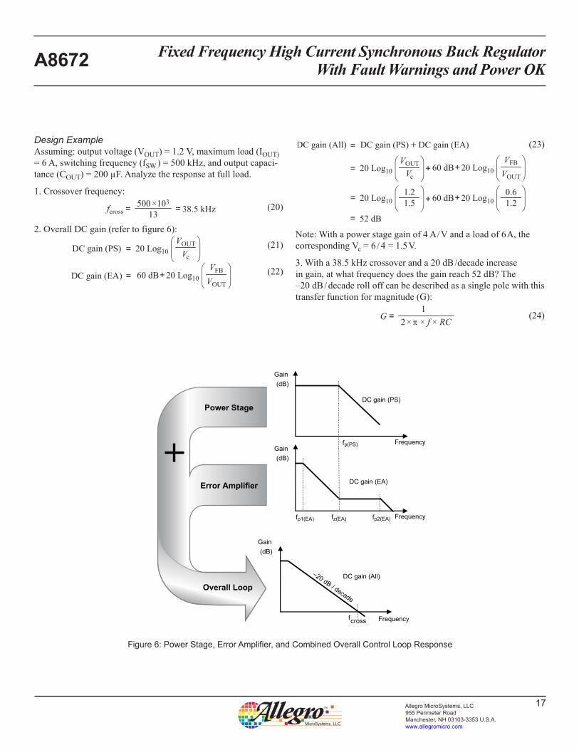
Control Loop Design ApproachThere are many different approaches to designing the feedback loop. The optimum solution is to select a target phase margin and bandwidth for optimum transient response. This typically requires either simulation software or detailed Bode plot analysis to generate a solution.
The particular approach described here derives a solution through a series of basic calculations. This approach aims for a simple –20dB/decaderolloff,fromthelowfrequencyerroramplifierpole (fp1(EA) ) to the 0 dB crossover point (fcross ). The 0 dB cross-over point is aimed at a thirteenth of the switching frequency (fSW). This factor is chosen as a compromise between good band-width and minimizing the phase lag introduced by the second power pole, which occurs between 1/3 and 1/6 of the switching frequency. In theory, this should introduce a phase margin of 90°, however, in practice it will be slightly less, due to the effects of the second power pole. The introduction of this second pole reduces the phase margin below 90°.
It is recommended that the error amplifier high frequency pole should be positioned one octave below the switching frequency. This provides some attenuation of the switching ripple whilst having minimum impact on the closed loop response.
Toachievea–20dB/decaderolloff,theerroramplifierzeroispositioned to coincide with the power pole at maximum load.
Figure 6 illustrates the power stage gain, the error amplifier gain, and then the combined overall loop response (power stage and error amplifier).
Fixed Frequency High Current Synchronous Buck Regulator With Fault Warnings and Power OKA8672
17Allegro MicroSystems, LLC 955 Perimeter Road Manchester, NH 03103-3353 U.S.A.www.allegromicro.com
Design Example Assuming: output voltage (VOUT) = 1.2 V, maximum load (IOUT) = 6 A, switching frequency (fSW)=500kHz,andoutputcapaci-tance(COUT)=200µF.Analyzetheresponseatfullload.
1.Crossoverfrequency:
38.5 kHzfcross 13 == 500 ×103
(20)
2.OverallDCgain(refertofigure6):
20 Log10 Vc=
VOUTDC gain (PS)
(21)
= 60 dB+20 Log10 VOUT
VFBDC gain (EA)
(22)
=
20 Log10 Vc=
VOUT 60 dB+20 Log10 VOUT
VFB
60 dB20 Log10
DC gain (All) DC gain (PS) + DC gain (EA)
=
52 dB=
+
+ +1.21.5
0.61.220 Log10
(23)
Note:Withapowerstagegainof4A/Vandaloadof6A,thecorresponding Vc=6/4=1.5V.
3.Witha38.5kHzcrossoveranda20dB/decadeincreasein gain, at what frequency does the gain reach 52 dB? The –20dB/decaderolloffcanbedescribedasasinglepolewiththistransfer function for magnitude (G):
G
1= 2 × × f × RC
(24)
Figure 6: Power Stage, Error Amplifier, and Combined Overall Control Loop Response
Gain(dB)
Gain(dB)
Gain(dB)
fp(PS)
fp1(EA) fp2(EA)fz(EA)
fcross
–20 dB / decade
Frequency
Frequency
Frequency
Power Stage
Error Amplifier
Overall Loop
DC gain (PS)
DC gain (EA)
DC gain (All)
Fixed Frequency High Current Synchronous Buck Regulator With Fault Warnings and Power OKA8672
18Allegro MicroSystems, LLC 955 Perimeter Road Manchester, NH 03103-3353 U.S.A.www.allegromicro.com
3a.Weknowthatat38.5kHzthegainis0dB(1).ThereforetheconstantRCcanbeworkedout:
RC1
= 2 × × 38.5 ×103 × 1= 4.13 ×10 – 6
(25)
3b.Amagnitudeof52dBrequiresagainof398.Theerrorampli-fier pole (fp1(EA)),thefrequencyatwhich398isreached,is:
fp1(EA)1
96.8 Hz
= 2 × × 4.13 ×10 – 6 × 398=
(26)
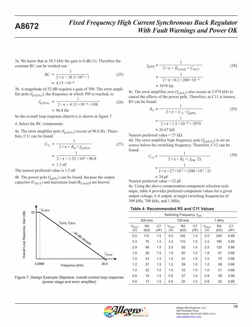
Sotheoverallloopresponseobjectiveisshowninfigure7.
4.SelecttheRCcomponents.
4a. The error amplifier pole (fp1(EA))occursat96.8Hz.There-fore,C11canbefound:
1= 2 × × 1.25 ×10 6 × 96.8
C111
= 2 × × RO × fp1(EA)
1.3 nF=
(27)
The nearest preferred value is 1.5 nF.4b. The power pole (fp(PS) ) can be found, because the output capacitor(COUT)andmaximumload(RLOAD) are known:
1= 2 × × 0.2 × 200 ×10 –6
fp(PS)1
= 2 × × RLOAD × COUT
3979 Hz=
(28)
4c. The error amplifier zero (fz(EA) )alsooccursat3.979kHztocanceltheeffectsofthepowerpole.Therefore,asC11isknown,R5canbefound:
1= 2 × × 1.5 ×10 –9 × 3979
R51
= 2 × × C11 × fp(PS)
26.67 kΩ=
(29)
Nearestpreferredvalue=27kΩ.4d. The error amplifier high frequency pole (fp2(EA) ) is set an octavebelowtheswitchingfrequency.Therefore,C12canbefound:
1= 2 × × 27 ×10 3 × (500 ×10 3 / 2)
C121
= 2 × × R5 × ( fSW /2)
24 pF=
(30)
Nearest preferred value = 22 pF.4e. Using the above compensation component selection tech-nique, table 4 provides preferred component values for a given output voltage, 6 A output, at target switching frequencies of 500kHz,700kHz,and1MHz.
Table 4: Recommended R5 and C11 ValuesSwitching Frequency, fSW
500 kHz 700 kHz 1 MHz
VOUT (V)
R4 (kΩ)
C7 (nF)
VOUT (V)
R4 (kΩ)
C7 (nF)
VOUT (V)
R4 (kΩ)
C7 (nF)
5.0 110 1.5 5.0 162 1.0 5.0 240 0.68
3.3 75 1.5 3.3 110 1.0 3.3 160 0.68
2.5 56 1.5 2.5 82 1.0 2.5 120 0.68
1.8 39 1.5 1.8 62 1.0 1.8 91 0.68
1.5 33 1.5 1.5 51 1.0 1.5 75 0.68
1.2 27 1.5 1.2 39 1.0 1.2 59 0.68
1.0 22 1.5 1.0 33 1.0 1.0 51 0.68
0.8 18 1.5 0.8 27 1.0 0.8 39 0.68
0.6 13 1.5 0.6 20 1.0 0.6 20 0.68
fcross
38.5
–20 dB / decade
Ove
rall
Loop
Res
pons
e, G
ain
(dB
)
0.0968
52fp1(EA)
fp(PS), fz(EA)
Frequency (kHz)
Figure 7: Design Example Objective: overall control loop response (power stage and error amplifier)
Fixed Frequency High Current Synchronous Buck Regulator With Fault Warnings and Power OKA8672
19Allegro MicroSystems, LLC 955 Perimeter Road Manchester, NH 03103-3353 U.S.A.www.allegromicro.com
Thermal ConsiderationsForagivensetofconditions,thejunctiontemperatureoftheA8672 can be estimated by carrying out a few calculations. This is important to ensure an adequate safety margin with respect to themaximumjunctiontemperature(150°C)toenhancereliabil-ity. This exercise also helps to understand the overall efficiency of the regulator.
The general approach is to work out what thermal impedance (RθJ-A)isrequiredtomaintainthejunctiontemperatureatagivenlevel, for a particular power dissipation. It should be noted that this process is usually iterative to achieve the optimum solution.
The following steps can be used as a guideline for determining a suitable thermal solution. First, estimate the maximum ambient temperature (TA)oftheapplication.Second,definethemaximumjunctiontemperature(TJ ). Note that the absolute maximum is 150°C.Third,determinetheworstcasepowerdissipation.Thiswill typically occur at maximum load and minimum VIN.
Design Example Assuming: input voltage (VIN ) = 12 V, output voltage (VOUT) = 1.2 V, maximum load (IOUT) = 6 A, switching frequency (fSW ) =500kHz,targetjunctiontemperature(TJ)≤125ºC,maximumambient temperature (TA)=85°C,andinductiveresistance(DCRL)=6.7mΩ.
1. The main power loss contributors are calculated separately:
•Switch static losses
a.EstimatetheRDS(on) of the high-side switch at the maximum targetjunctiontemperature:
=125 – 25
200
200
20 × 10 –3
= 0.03 Ω
=TJ – 25
RDS(on)HS(TJ) RDS(on)HS(25C) 1 +
1 +
(31)
whereRDS(on)HS(25C)istheRDS(on)HSvalue that can be found fromtheElectricalCharacteristicstableinthisdatasheet.
b.EstimatetheRDS(on)ofthelowsideswitchatthegivenjunc-tion temperature:
=125 – 25
200
200
8 × 10 –3
= 0.012 Ω
=TJ – 25
RDS(on)LS(TJ) RDS(on)LS(25C) 1 +
1 +
(32)
whereRDS(on)LS(25C)istheRDS(on)LSvalue that can be found from
theElectricalCharacteristicstableinthisdatasheet.
c.Estimatethedutycycle(D)byapplyingequation3(ton ):
1.2 + (0.012 + 0.0067 )
0.11
1=
=
12 + (0.012 – 0.03 ) 500 103500 1036
6
VOUT + (RDS(on)LS + DCRL ) VIN + (RDS(on)LS – RDS(on)HS )
IOUT 1=
=
IOUT fSWfSW
D ton × fSW
(33)
d. The high side static loss can be determined:
= 62 × 0.11 × 0.03= 0.119 W
PstaticHI = I 2OUT × D × RDS(on)HS(TJ)
(34)
e. The low side static loss can be determined:
= 62 × (1 – 0.11) × 0.012= 0.385 W
PstaticLO = I 2OUT × 1 – D × RDS(on)LS(TJ)
(35)
•Switching losses The combined turn on and turn off losses for
both switches are calculated as:
122
= × 6 × 6 ×10 –9 × 500 ×103 × 2
= 0.216 W
PswitchVIN
2= × I OUT × 6 ×10 –9 × fSW × 2
(36)
Fixed Frequency High Current Synchronous Buck Regulator With Fault Warnings and Power OKA8672
20Allegro MicroSystems, LLC 955 Perimeter Road Manchester, NH 03103-3353 U.S.A.www.allegromicro.com
•Recirculation diode losses The recirculation diode losses (low-side switch) are calculated as:
==
0.8 × 6 × 6 ×10 –9 × 500 ×103
= 0.014 W
Precirc 0.8 × I OUT × 6 ×10 –9 × fSW
(37)
•Diode transit losses The recirculation diode losses (low-side switch) are calculated as:
== 12 × 6 × 3 ×10 –9 × 500 ×103
= 0.108 W
Ptransit VIN × I OUT × 3 ×10 –9 × fSW
(38)
•BIAS losses The supply bias losses are calculated as:
==
0.24 WPbias VIN × 20 × 10 –3
(39)
2. The total losses in the A8672 can be estimated:
Ptotal = PstaticHI + PstaticLO + Pswitch + Precirc + Ptransit + Pbias (40) =0.119+0.385 + 0.216 + 0.014 + 0.108 + 0.24 = 1.082 W3.Thethermalimpedancerequiredforthesolutioncanbefound:
=
=
RθJA TJ – TA Ptotal
125 – 85 1.082
= 37 °C/W
(41)
For this particular solution, a high thermal efficiency board is requiredtoensurethejunctiontemperatureiskeptbelow125°C.ItisrecommendedtouseaPCBwithatleastfourlayers.TheA8672 should be mounted onto a thermal pad. A number of vias should connect the thermal pad to at least one of the internal lay-ersandthebottomsideofthePCB.Bothoftheselayersshouldbeagroundplane.SeetheLayoutsectionformoreinformation.
Regulator EfficiencyThe overall regulator efficiency can be determined by including the inductor loss. In the above thermal characteristics example, theinductorresistance,DCRL=6.7mΩ.Thereforetheinductorpower loss can be found::
==
PL DCRL × I 2OUT 0.0067 × 62
= 0.241 W
(42)
The overall regulator efficiency can be found:
=
=
η VOUT × IOUT
(VOUT × IOUT ) + Ptotal+ PL 1.2 × 6
(1.2 × 6) + 1.082 + 0.241
= 84.5 %
(43)
Fixed Frequency High Current Synchronous Buck Regulator With Fault Warnings and Power OKA8672
21Allegro MicroSystems, LLC 955 Perimeter Road Manchester, NH 03103-3353 U.S.A.www.allegromicro.com
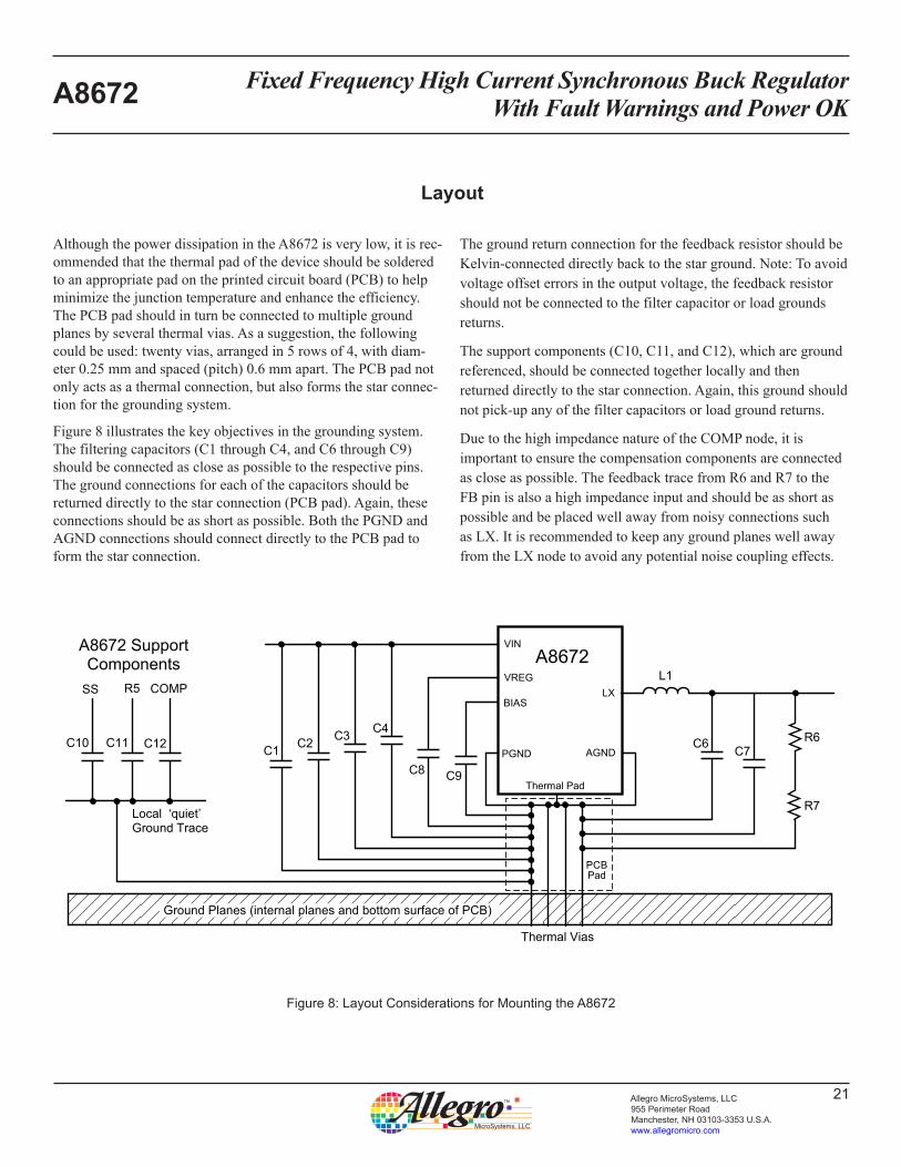
Layout
Although the power dissipation in the A8672 is very low, it is rec-ommended that the thermal pad of the device should be soldered toanappropriatepadontheprintedcircuitboard(PCB)tohelpminimizethejunctiontemperatureandenhancetheefficiency.ThePCBpadshouldinturnbeconnectedtomultiplegroundplanes by several thermal vias. As a suggestion, the following could be used: twenty vias, arranged in 5 rows of 4, with diam-eter0.25mmandspaced(pitch)0.6mmapart.ThePCBpadnotonly acts as a thermal connection, but also forms the star connec-tion for the grounding system.
Figure8illustratesthekeyobjectivesinthegroundingsystem.Thefilteringcapacitors(C1throughC4,andC6throughC9)should be connected as close as possible to the respective pins. The ground connections for each of the capacitors should be returneddirectlytothestarconnection(PCBpad).Again,theseconnectionsshouldbeasshortaspossible.BoththePGNDandAGNDconnectionsshouldconnectdirectlytothePCBpadtoform the star connection.
The ground return connection for the feedback resistor should be Kelvin-connected directly back to the star ground. Note: To avoid voltage offset errors in the output voltage, the feedback resistor should not be connected to the filter capacitor or load grounds returns.
Thesupportcomponents(C10,C11,andC12),whicharegroundreferenced, should be connected together locally and then returned directly to the star connection. Again, this ground should not pick-up any of the filter capacitors or load ground returns.
DuetothehighimpedancenatureoftheCOMPnode,itisimportant to ensure the compensation components are connected ascloseaspossible.ThefeedbacktracefromR6andR7totheFB pin is also a high impedance input and should be as short as possible and be placed well away from noisy connections such as LX. It is recommended to keep any ground planes well away from the LX node to avoid any potential noise coupling effects.
Figure 8: Layout Considerations for Mounting the A8672
A8672
Ground Planes (internal planes and bottom surface of PCB)
Thermal Vias
A8672 Support Components
Local ‘quiet’ Ground Trace
SS
C11 PGND
Thermal Pad
PCBPad
VREG
VIN
LXBIAS
C12 C10
R5 COMP
AGNDR6
R7
C1 C2
C9 C8
C4 C3
L1
C6 C7
Fixed Frequency High Current Synchronous Buck Regulator With Fault Warnings and Power OKA8672
22Allegro MicroSystems, LLC 955 Perimeter Road Manchester, NH 03103-3353 U.S.A.www.allegromicro.com
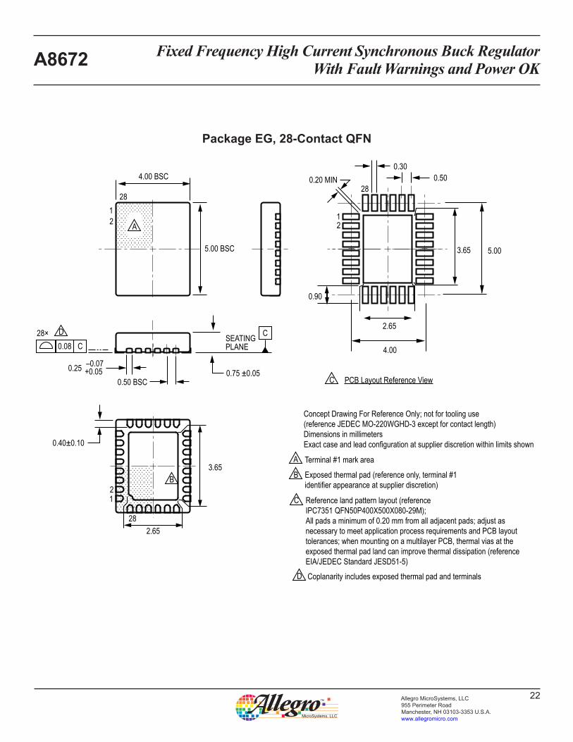
Package EG, 28-Contact QFN
28
28
21
21
A
A Terminal #1 mark area
B Exposed thermal pad (reference only, terminal #1 identifier appearance at supplier discretion)
Concept Drawing For Reference Only; not for tooling use(reference JEDEC MO-220WGHD-3 except for contact length)Dimensions in millimetersExact case and lead configuration at supplier discretion within limits shown
C Reference land pattern layout (reference IPC7351 QFN50P400X500X080-29M); All pads a minimum of 0.20 mm from all adjacent pads; adjust as necessary to meet application process requirements and PCB layout tolerances; when mounting on a multilayer PCB, thermal vias at the exposed thermal pad land can improve thermal dissipation (reference EIA/JEDEC Standard JESD51-5)
B
28
21
PCB Layout Reference View0.50 BSC
4.00 BSC
5.00 BSC
0.75 ±0.050.25
0.40±0.10
0.300.20 MIN 0.50
0.90
5.00
4.00
C
3.65
2.65
2.65
3.65
C0.0828× SEATING
PLANECD
D Coplanarity includes exposed thermal pad and terminals
–0.07+0.05
Fixed Frequency High Current Synchronous Buck Regulator With Fault Warnings and Power OKA8672
23Allegro MicroSystems, LLC 955 Perimeter Road Manchester, NH 03103-3353 U.S.A.www.allegromicro.com
For the latest version of this document, visit our website:www.allegromicro.com
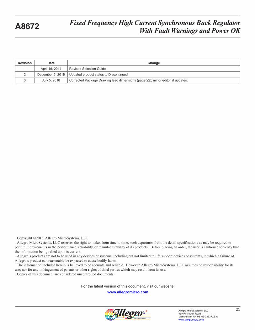
Revision Date Change1 April 16, 2014 Revised Selection Guide
2 December 5, 2016 Updated product status to Discontinued
3 July 5, 2018 Corrected Package Drawing lead dimensions (page 22); minor editorial updates.
Copyright ©2018, Allegro MicroSystems, LLCAllegro MicroSystems, LLC reserves the right to make, from time to time, such departures from the detail specifications as may be required to
permit improvements in the performance, reliability, or manufacturability of its products. Before placing an order, the user is cautioned to verify that the information being relied upon is current.
Allegro’s products are not to be used in any devices or systems, including but not limited to life support devices or systems, in which a failure of Allegro’s product can reasonably be expected to cause bodily harm.
The information included herein is believed to be accurate and reliable. However, Allegro MicroSystems, LLC assumes no responsibility for its use; nor for any infringement of patents or other rights of third parties which may result from its use.
Copies of this document are considered uncontrolled documents.