Embed Size (px)
Citation preview
AB32 Transistor Series Voltage Regulator
Analog LabExperiment Board
Ver. 1.0
QUALITY POLICY
To be a Global Provider of Innovative and Affordable Electronic Equipments for Technology Training by enhancing Customer Satisfaction based on Research, Modern manufacturing techniques and continuous improvement in Quality of the products and Services with active participation of employees.
An ISO 9001: 2000 company
94-101, Electronic Complex, Pardesipura INDORE-452010, India.Tel.: 91-731-2570301 Fax: 91-731-2555643Email: [email protected] Web: www.scientech.bz
AB32
Scientech Technologies Pvt. Ltd. 2

AB32
Transistor Series Voltage RegulatorAB32
TABLE OF CONTENTS
1.Introduction 4
2. Theory 6
3.Experiments
• Experiment 1 10To study transistor series voltage regulator, when
input voltage Vin is fixed while Load resistance RL
is variable.
• Experiment 2 13To study transistor series voltage regulator, wheninput voltage Vin is variable while Load resistance RL
is fixed.
4.Datasheet 15
5.Warranty 16
6.List of Service Centers 17
7.List of Accessories with AB32 18
8. Notes 19
Scientech Technologies Pvt. Ltd. 3
AB32
INTRODUCTION
AB32 is a compact, ready to use Transistor Series Voltage Regulator experiment board. This is useful for students to study the operation of Transistor as a voltage regulator when it is connected in series. It can be used as stand alone unit with external DC power supply or can be used with SCIENTECH Analog Lab ST2612 which has built in DC power supply, AC power supply, function generator, modulation generator, continuity tester, toggle switches, and potentiometer.
List of Boards :
Model Name
AB01 Diode characteristics (Si, Zener, LED)AB02 Transistor characteristics (CB NPN)AB03 Transistor characteristics (CB PNP)AB04 Transistor characteristics (CE NPN)AB05 Transistor characteristics (CE PNP)AB06 Transistor characteristics (CC NPN)AB07 Transistor characteristics (CC PNP)AB08 FET characteristicsAB09 Rectifier CircuitsAB10 Wheatstone BridgeAB11 Maxwell’s BridgeAB14 Darlington PairAB15 Common Emitter AmplifierAB16 Common Collector AmplifierAB17 Common Base AmplifierAB18 Cascode AmplifierAB19 RC-Coupled AmplifierAB20 Direct Coupled AmplifierAB21 Class a AmplifierAB22 Class B Amplifier (push pull emitter follower)AB23 Class C Tuned AmplifierAB25 Phase Locked Loop (FM Demodulator & Frequency
Divider / Multiplier)AB28 Multivibrator ( Mono stable / Astable)AB29 F-V and V-F ConverterAB30 V-I and I-V ConverterAB31 Zener Voltage Regulator AB33 Transistor Shunt Voltage Regulator
Scientech Technologies Pvt. Ltd. 4
AB32
AB41 Differential Amplifier (Transistorized)AB42 Operational Amplifier (Inverting / Non-inverting /
Differentiator)AB43 Operational Amplifier (Adder/Scalar)AB44 Operational Amplifier (Integrator/ Differentiator)AB45 Schmitt Trigger and ComparatorAB51 Active filters (Low Pass and High Pass)AB52 Active Band Pass Filter AB53 Notch Filter AB54 Tschebyscheff FilterAB56 Fiber Optic Analog LinkAB65 Phase Shift OscillatorAB66 Wien Bridge OscillatorsAB67 Colpitt OscillatorAB68 Hartley OscillatorAB80 RLC Series and RLC Parallel Resonance AB81 Kirchoff’s Laws (Kirchhoff’s Current Law & Kirchhoff’s
Voltage Law)AB82 Thevenin’s and Maximum power Transfer TheoremAB83 Reciprocity and Superposition TheoremAB84 Tellegen’s TheoremAB85 Norton’s theoremAB88 Diode ClipperAB89 Diode ClampersAB90 Two port network parameterAB91 Optical Transducer (Photovoltaic cell)AB92 Optical Transducer (Photoconductive cell/LDR)AB93 Optical Transducer (PhotoTransistor)AB96 Temperature Transducer (RTD & IC335)AB97 Temperature Transducer (Thermocouple)AB101 DSB Modulator and DemodulatorAB102 SSB Modulator and DemodulatorAB106 FM Modulator and Demodulator
………… and many more
Scientech Technologies Pvt. Ltd. 5
AB32
THEORY
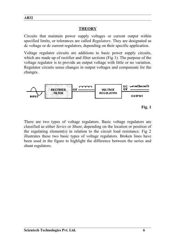
Circuits that maintain power supply voltages or current output within specified limits, or tolerances are called Regulators. They are designated as dc voltage or dc current regulators, depending on their specific application.
Voltage regulator circuits are additions to basic power supply circuits, which are made up of rectifier and filter sections (Fig 1). The purpose of the voltage regulator is to provide an output voltage with little or no variation. Regulator circuits sense changes in output voltages and compensate for the changes.
Fig. 1
There are two types of voltage regulators. Basic voltage regulators are classified as either Series or Shunt, depending on the location or position of the regulating element(s) in relation to the circuit load resistance. Fig 2 illustrates these two basic types of voltage regulators. Broken lines have been used in the figure to highlight the difference between the series and shunt regulators.
Scientech Technologies Pvt. Ltd. 6

AB32
Fig. 2
The schematic drawing in view B is that of a series regulator. It is called series regulator because the regulating device is connected in series with the load resistance. Fig 2 illustrates the principle of series voltage regulation. From the figure it is clear that the regulator is in series with the load resistance (RL) and that the fixed resistor (RS) is in series with the load resistance. You already know the voltage drop across affixed resistor remains constant unless the current flowing through it varies (increases or decreases).
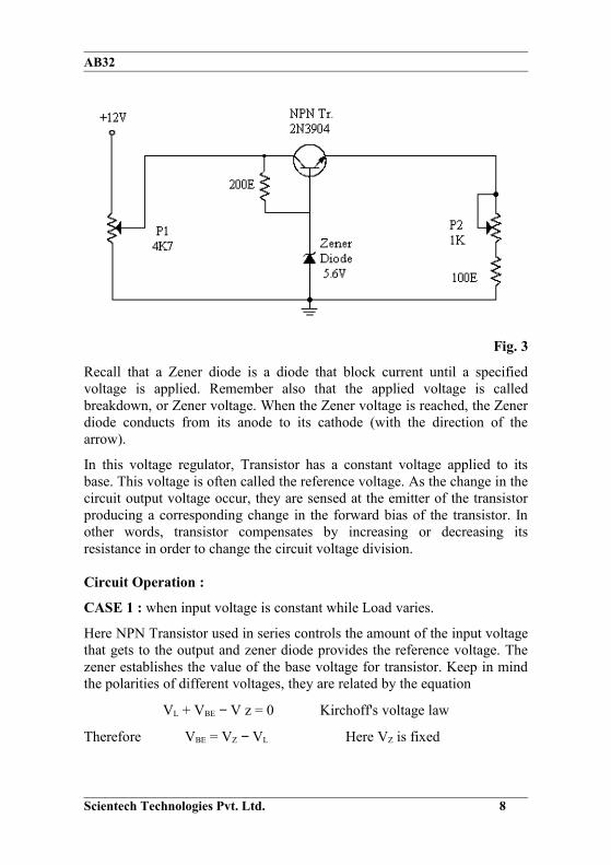
The schematic for a typical series voltage regulator is shown in Fig3. Notice that this regulator has a NPN transistor 2N3904 in place of the variable resistor found in Fig 2.
Because the total load current passes through this transistor, it is sometimes called a ‘‘pass transistor’’. Other components, which make up the circuit, are the current limiting resistor of 200Ω and the Zener diode of 5.6V
Scientech Technologies Pvt. Ltd. 7
AB32
Fig. 3
Recall that a Zener diode is a diode that block current until a specified voltage is applied. Remember also that the applied voltage is called breakdown, or Zener voltage. When the Zener voltage is reached, the Zener diode conducts from its anode to its cathode (with the direction of the arrow).
In this voltage regulator, Transistor has a constant voltage applied to its base. This voltage is often called the reference voltage. As the change in the circuit output voltage occur, they are sensed at the emitter of the transistor producing a corresponding change in the forward bias of the transistor. In other words, transistor compensates by increasing or decreasing its resistance in order to change the circuit voltage division.
Circuit Operation :
CASE 1 : when input voltage is constant while Load varies.
Here NPN Transistor used in series controls the amount of the input voltage that gets to the output and zener diode provides the reference voltage. The zener establishes the value of the base voltage for transistor. Keep in mind the polarities of different voltages, they are related by the equation
VL + VBE − V z = 0 Kirchoff's voltage law
Therefore VBE = VZ − VL Here VZ is fixed
Scientech Technologies Pvt. Ltd. 8
AB32
The output voltage across load will equal the zener voltage minus a 0.7-volt drop across the forward biased base-emitter junction of transistor, or 4.9V (5.6 − 0.7).
When current demand is increased by decreasing RL, VL tends to decrease. It will increase VBE because VZ is fixed. This will increase forward bias of the transistor thereby increasing its level of conduction. This will lead to decrease in the collector-emitter resistance of the transistor which will slightly increase the input current to compensate for decrease in RL so that VL = ILRL will remain at constant value.
CASE 2 : when input voltage varies while Load remains constant.
When the input voltage increases, output voltage across increases momentarily. This momentarily deviation or variation, from the required regulated output voltage of 4.9 volts is a result of a rise in the input voltage. Since the base voltage of transistor is held at 5.6V by zener, that's why the forward bias of transistor decreases. Because this bias voltage is less than the normal 0.7 volts, the resistance of transistor increases, thereby increasing the voltage drop across the transistor.
This voltage drop restores the output voltage to the required regulated voltage of 4.9V.
Note :
1. Regulated output voltage might be slightly higher than the expected voltage due to tolerance of Zener diode.
Scientech Technologies Pvt. Ltd. 9
AB32
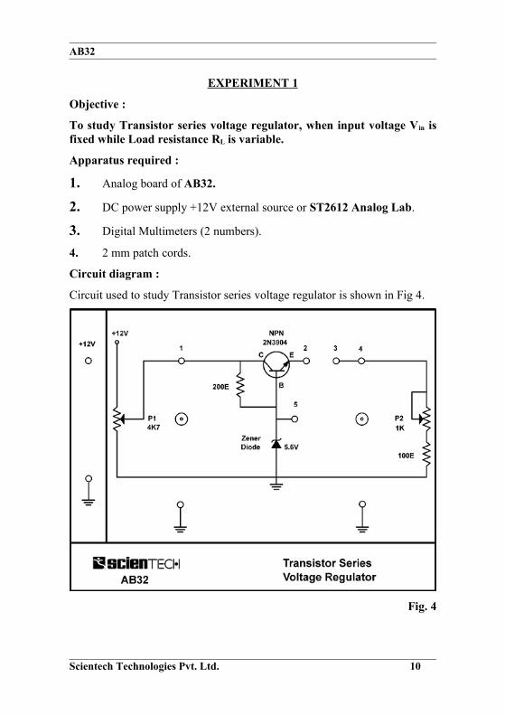
EXPERIMENT 1
Objective :
To study Transistor series voltage regulator, when input voltage Vin is fixed while Load resistance RL is variable.
Apparatus required :
1. Analog board of AB32.
2. DC power supply +12V external source or ST2612 Analog Lab.
3. Digital Multimeters (2 numbers).
4. 2 mm patch cords.
Circuit diagram :
Circuit used to study Transistor series voltage regulator is shown in Fig 4.
Fig. 4
Scientech Technologies Pvt. Ltd. 10
AB32
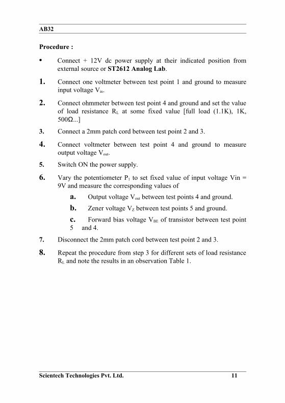
Procedure :
• Connect + 12V dc power supply at their indicated position from external source or ST2612 Analog Lab.
1. Connect one voltmeter between test point 1 and ground to measure input voltage Vin.
2. Connect ohmmeter between test point 4 and ground and set the value of load resistance RL at some fixed value [full load (1.1K), 1K, 500Ω...]
3. Connect a 2mm patch cord between test point 2 and 3.
4. Connect voltmeter between test point 4 and ground to measure output voltage Vout.
5. Switch ON the power supply.
6. Vary the potentiometer P1 to set fixed value of input voltage Vin = 9V and measure the corresponding values of
a. Output voltage Vout between test points 4 and ground.
b. Zener voltage VZ between test points 5 and ground.
c. Forward bias voltage VBE of transistor between test point 5 and 4.
7. Disconnect the 2mm patch cord between test point 2 and 3.
8. Repeat the procedure from step 3 for different sets of load resistance RL and note the results in an observation Table 1.
Scientech Technologies Pvt. Ltd. 11
AB32
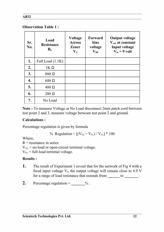
Observation Table 1 :
Sr.No.
LoadResistance
RL
VoltageAcrossZener
VZ
Forwardbias
voltageVBE
Output voltageVout at constantInput voltage
Vin = 9 volt
1. Full Load (1.1K)2. 1K Ω3. 800 Ω
4. 600 Ω
5. 400 Ω6. 200 Ω
7. No Load
Note : To measure Voltage at No Load disconnect 2mm patch cord between test point 2 and 3, measure voltage between test point 2 and ground.
Calculations :
Percentage regulation is given by formula
% Regulation = [(VNL − VFL) / VFL] * 100Where,R = resistance in seriesVNL = no-load or open-circuit terminal voltage. VFL = full-load terminal voltage.
Results :
1. The result of Experiment 1 reveal that for the network of Fig 4 with a fixed input voltage Vin the output voltage will remain close to 4.9 V for a range of load resistance that extends from ______ to _______ .
2. Percentage regulation = _______% .
Scientech Technologies Pvt. Ltd. 12

AB32
EXPERIMENT 2
Objective :
To study Transistor series voltage regulator, when input voltage Vin is variable while Load resistance RL is fixed.
Apparatus required :
1. Analog board of AB32.
2. DC power supply +12V external source or ST2612 Analog Lab.
3. Digital Multimeters (2 numbers).
4. 2 mm patch cords.
Circuit diagram :
Circuit used to study Transistor series voltage regulator is shown in Fig 5.
Fig. 5
Scientech Technologies Pvt. Ltd. 13
AB32
Procedure :
• Connect +12V dc power supply at their indicated position from external source or ST2612 Analog Lab.
1. Connect one voltmeter between test point 1 and ground to measure input voltage Vin
2. Connect ohmmeter between test point 4 and ground and set the value of load resistance RL at maximum value.
3. Connect a 2mm patch cord between test point 2 and 3.
4. Connect voltmeter between test point 4 and ground to measure output voltage Vout.
5. Switch ON the power supply.
6. Vary the potentiometer P1 to set fixed value of input voltage Vin = 7V, 8V, 9V… and measure the corresponding values of
a. Output voltage Vout between test points 4 and ground. b. Zener voltage Vz between test points 5 and ground. c. Forward bias voltage VBE of transistor between test point 5 and 4.
7. Repeat the procedure from step 7 for different sets of input voltage Vin and note the results in an observation Table 2.
Observation Table 2 :
Sr.No.
InputVoltage
Vin
VoltageAcross
Zener VZ
Forwardbias
voltage VBE
Output voltageVout at fixed load
resistance RL = Max1. 7 V2. 8 V3. 9 V4. 10 V5. 11 V
Results :
Scientech Technologies Pvt. Ltd. 14
AB32
1. The result of Experiment 2 reveal that for the network of Fig 5 with a fixed Load resistance, the output voltage will remain close to 4.9V for a range of input voltage Vin that extends from _____ to_____ .
Scientech Technologies Pvt. Ltd. 15
AB32
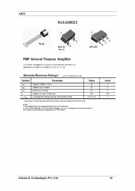
DATASHEET
Scientech Technologies Pvt. Ltd. 16
AB32
WARRANTY
1) We guarantee the instrument against all manufacturing defects during 24 months from the date of sale by us or through our dealers.
2) The guarantee covers manufacturing defects in respect of indigenous components and material limited to the warranty extended to us by the original manufacturer, and defect will be rectified as far as lies within our control.
3) The guarantee will become INVALID.a)If the instrument is not operated as per instruction given in the
instruction manual. b)If the agreed payment terms and other conditions of sale are not
followed.c) If the customer resells the instrument to another party.d)Provided no attempt have been made to service and modify the
instrument.4) The non-working of the instrument is to be communicated to us
immediately giving full details of the complaints and defects noticed specifically mentioning the type and sr. no. of the instrument, date of purchase etc.
5) The repair work will be carried out, provided the instrument is dispatched securely packed and insured with the railways. To and fro charges will be to the account of the customer.
DESPATCH PROCEDURE FOR SERVICEShould it become necessary to send back the instrument to factory please observe the following procedure:1) Before dispatching the instrument please write to us giving full
details of the fault noticed.2) After receipt of your letter our repairs dept. will advise you whether
it is necessary to send the instrument back to us for repairs or the adjustment is possible in your premises.
Dispatch the instrument (only on the receipt of our advice) securely packed in original packing duly insured and freight paid along with accessories and a copy of the details noticed to us at our factory address.
Scientech Technologies Pvt. Ltd. 17
AB32
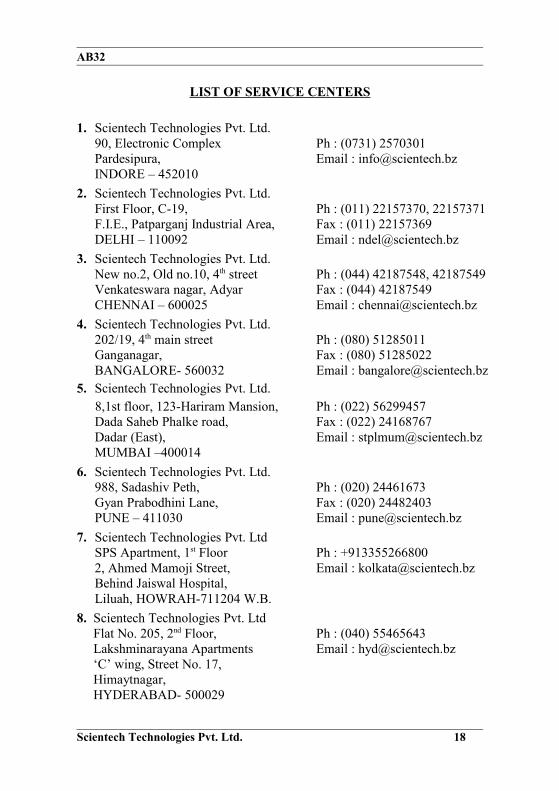
LIST OF SERVICE CENTERS
1. Scientech Technologies Pvt. Ltd.90, Electronic Complex Ph : (0731) 2570301Pardesipura, Email : [email protected] INDORE – 452010
2. Scientech Technologies Pvt. Ltd.First Floor, C-19, Ph : (011) 22157370, 22157371F.I.E., Patparganj Industrial Area, Fax : (011) 22157369DELHI – 110092 Email : [email protected]
3. Scientech Technologies Pvt. Ltd.New no.2, Old no.10, 4th street Ph : (044) 42187548, 42187549
Venkateswara nagar, Adyar Fax : (044) 42187549CHENNAI – 600025 Email : [email protected]
4. Scientech Technologies Pvt. Ltd. 202/19, 4th main street Ph : (080) 51285011 Ganganagar, Fax : (080) 51285022 BANGALORE- 560032 Email : [email protected]. Scientech Technologies Pvt. Ltd.
8,1st floor, 123-Hariram Mansion, Ph : (022) 56299457 Dada Saheb Phalke road, Fax : (022) 24168767 Dadar (East), Email : [email protected] MUMBAI –400014 6. Scientech Technologies Pvt. Ltd. 988, Sadashiv Peth, Ph : (020) 24461673 Gyan Prabodhini Lane, Fax : (020) 24482403 PUNE – 411030 Email : [email protected]. Scientech Technologies Pvt. Ltd SPS Apartment, 1st Floor Ph : +913355266800 2, Ahmed Mamoji Street, Email : [email protected]
Behind Jaiswal Hospital, Liluah, HOWRAH-711204 W.B.8. Scientech Technologies Pvt. Ltd Flat No. 205, 2nd Floor, Ph : (040) 55465643 Lakshminarayana Apartments Email : [email protected] ‘C’ wing, Street No. 17, Himaytnagar, HYDERABAD- 500029
Scientech Technologies Pvt. Ltd. 18

AB32
LIST OF ACCESSORIES
1. 2mm Patch cord (red) .........................................................1 Nos.
2. 2mm Patch cord (black) ......................................................1 Nos.
3. 2mm Patch cord (blue) .....................................................1 Nos.
Scientech Technologies Pvt. Ltd. 19

AB32
NOTES
Scientech Technologies Pvt. Ltd. 20
AB32
NOTES
Scientech Technologies Pvt. Ltd. 21