Embed Size (px)
Citation preview

A Bipolar 16K ROMUtilizing Schottky Diode Cells
J. F. Gunn, D. J. Lynes, and R. L. PritchettBell Telephone Laboratories
Introduction
As bipolar circuits assume more of a role in microprocessororiented systems, it becomes advantageous to extend theapplication of bipolar technology to a large mask program-mable ROM. This paper will describe a 16K bipolar ROM,organized as 2K x 8 bits, which utilizes for its basic memorycell a simple and compact Schottky diode.Our specific choice of bipolar chip fabrication technology
is the triple-diffused GIMIC' structure which providesgood speed-power performance and high packing density.By combining the Schottky diode cell with this technology,we have achieved access times of 150 nsec at a power dissi-pation of 175 mW from a single 5V supply.
Why a bipolar ROM? With so many good NMOS read-only memories available today, why choose a bipolarstructure for a large ROM? The reason for our choice isthat a bipolar ROM has the potential for higher speed forthe same power, chip size, and cost as its NMOS counter-part. Additionally, because GIMIC circuits have all theusual bipolar attributes, this ROM easily meets the fullTTL fan-out requirement and can thus reduce systempackage count by eliminating buffer circuits. Inputs, onthe other hand, are designed for very low current, NMOS-compatible operation.
It should be emphasized that the present level of speedperformance was chosen simply to be somewhat fasterthan current MOS circuits, so that in no present-dayMOS microprocessor applications would the speed of the16K ROM be a limiting factor for system designs. Withincreased usage of even faster microprocessors, there maybe a need for an even higher speed ROM. Within the con-text of the present design, significantly higher speedsthan the present 150 nsec can be achieved with additionalchip fabrication complexity, but with no penalty in chipsize or power.
As chip fabrication technology improves, particularlyphotolithographic tolerances, the lower limit of ROMaccess time will easily keep pace with new microprocessordevelopments. Increased photolithographic capability will,of course, also make the design of 32K and 65K bipolarROMs feasible while keeping chip size (cost) down, andstill retaining high performance levels.
The Schottky diode cell. Initially our choice of a Schottkydiode cell was based only on small size and simplicity;it is, after all, only a single contact window registeredsomewhere on an n-type silicon region. This makes aSchottky diode the smallest bipolar circuit element.Another advantage of the Schottky diode cell, however,soon became obvious: it is immune to emitter-collectorshorts. These shorts or "pipes" are randomly formedduring the emitter fabrication step of many bipolar pro-cesses, and the presence of these defects limits the yield oflarge bipolar circuits. Since most bipolar ROMs employemitter-follower cells, which are sensitive to emitter-collector shorts, the Schottky diode cell should-and webelieve does-offer a significant improvement in chip yield.The simplicity of the Schottky diode cell also lends itself
to higher yield because defects in some of the maskinglevels used to fabricate the ROM chip will not be fatal tothe cell. The diode window area, for instance, can vary bya factor of two and still provide a perfectly functional cell.
The triple-diffused technology, GIMIC. Of the manyfactors that went into the selection of the GIMIC bipolartechnology, size was again given the highest importance.In the triple-diffused structure shown in Figure 1, alllayers (emitter, base, and collector) are formed from thetop surface of the silicon by implantation and/or diffusion.In other bipolar technologies, the collector is formed as a*buried layer in the silicon. One of the properties of thetriple-diffused structure is that fewer dimensional toler-
COMPUTER14
ances are required to fabricate isolated collector (n-) regions.This means that the Schottky diode cells which are formedin n- regions can be packed more densely by utilizing atriple-diffused structure than would be possible with aburied-collector technology. Since the access circuits con-tain many isolated transistors, they also would have ahigher packing density because transistor isolation spacingis small.
Since only bulk silicon is used in the GIMIC technology,the defects associated with growing the epitaxial layersover buried collectors are simply not present. This featurebenefits the ROM in two ways. First, the Schottky diodeyield is improved because we don't try to form diodes overepitaxial defects. Secondly, emitter-collector "pipe" forma-tion is greatly inhibited for bulk Si, and this leads toimproved yield in the access circuits which are sensitiveto emitter-collector shorts.A triple-diffused technology generally offers other yield
advantages because fewer masking steps are required forchip fabrication, and this simplicity in manufacturing leadsdirectly to a lower cost per processed silicon wafer. Thus,high packing density and low defect fatality rate enhancethe number of good chips per wafer, while the simplicityof the GIMIC process lowers the cost per wafer.From the circuit point of view, however, the versatility
of this bipolar technology allows the designer a wide choiceof ECL, TTL, Schottky TTL, and other circuit forms. Thismeans that circuits totally internal to the chip and externalinterface circuits can each be separately optimized to dothe job required. In the present circuit, for instance, theinternal gates are mostly ECL, while to the outside world,the ROM looks like Schottky TTL at the outputs and hascurrent levels similar to NMOS on the inputs.
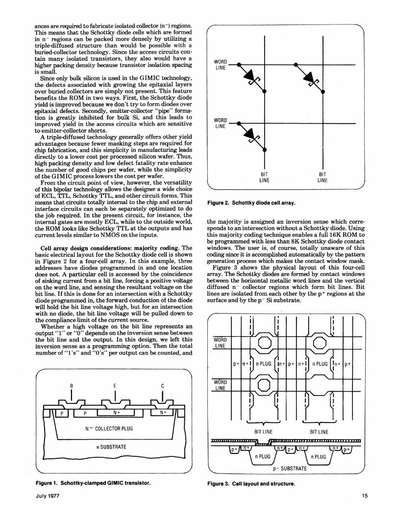
Cell array design considerations: majority coding. Thebasic electrical layout for the Schottky diode cell is shownin Figure 2 for a four-cell array. In this example, threeaddresses have diodes programmed in and one locationdoes not. A particular cell is accessed by the coincidenceof sinking current from a bit line, forcing a positive voltageon the word line, and sensing the resultant voltage on thebit line. If this is done for an intersection with a Schottkydiode programmed in, the forward conduction of the diodewill hold the bit line voltage high, but for an intersectionwith no diode, the bit line voltage will be pulled down tothe compliance limit of the current source.Whether a high voltage on the bit line represents an
output "1" or "0" depends on the inversion sense betweenthe bit line and the output. In this design, we left thisinversion sense as a programming option. Then the totalnumber of "l's" and "0's" per output can be counted, and
Figure 1. Schottky-clamped GIMIC transistor.
July 1977
Figure 2. Schottky diode cell array.
the majority is assigned an inversion sense which corre-sponds to an intersection without a Schottky diode. Usingthis majority coding technique enables a full 16K ROM tobe programmed with less than 8K Schottky diode contactwindows. The user is, of course, totally unaware of thiscoding since it is accomplished automatically by the patterngeneration process which makes the contact window mask.Figure 3 shows the physical layout of this four-cell
array. The Schottky diodes are formed by contact windowsbetween the horizontal metallic word lines and the verticaldiffused n- collector regions which form bit lines. Bitlines are isolated from each other by the p+ regions at thesurface and by the p- Si substrate.
Figure 3. Cell layout and structure.
15
WORDLINE
WORD In,
LINE
BIT BITLINE LINE
K
1-.1-1

Since the physical array is 128 word lines by 128 bitlines, the n- bit lines are long and narrow and would, bythemselves, lead to intolerably high series resistance. Forthis reason, an n+ emitter region is added to the bit linesto reduce resistance. Even with this added conductivity,however, the total bit line resistance is 5000 Q, and thisresistance in combination with the n+ - p+ sidewallcapacitance along the edge of the bit line creates an RCconstant of approximately 70 nsec that dominates the150-nsec access time of the ROM.Of course, a two-level metal system employed at this
point would eliminate much of this time constant, but itwas felt that the performance was adequate for all presentapplications without adding the additional cost of two-levelmetal processing. Furthermore, since two-level metalprocessing comes at the end of chip fabrication and aftercontact window coding, this would add to the turnaroundtime required to implement new program codes.
Access circuits-the key to high performance. Ratherthan trying to reduce the bit line RC constants, ourapproach is to minimize their effect by assuring that thebit lines make only small, well-controlled voltage excursions.This is done by driving the bit lines and word lines withECL-like access circuits powered from temperature-com-pensated, internally regulated supplies. Figure 4 shows aschematic layout of the access circuits. The low voltage onthe bit line, for instance, is set by the compliance of thetransistor current source, and this compliance limit isdetermined directly by the output voltage of the 1:16decoder. This decoder is entirely an ECL circuit whoseoutput "1" is 1.5 VBE (1 VBE = emitter-base forwardvoltage). Similarly, the base of the emitter-follower worddriver is driven from the 1:32 decoder whose output isderived from an NxVBE internal power supply. Finally,the sense amplifier is an ECL-like gate whose thresholdclosely tracks the minimum and maximum bit line voltages.Like other ECL gates, the sense amplifier has both outputand output complement readily available, and this is wherethe majority coding sense is selected. By selecting theoutput sense in this fashion, a minimum of extra circuitryis required and no extra stages of delay are incurred.
All internal ECL logic levels are generated by the ECLinput buffers shown in Figure 5. The voltage levels of the
Figure 4. Schematic access circuits.
16
3 VBE
INPUT
Vcc
ECL-LIKELOGIC LEVELS
I
Figure 5. Input buffer circuit.
emitter-follower outputs (for wired or logic) are directlyderived from the 3 VBE supply, as is the input threshold,VREF. VREF is simply set to a normal TTL threshold value,but the input current is not typical for a TTL gate. Theinput current is determined by the value of current sourcefor the differential pair divided by P of the input transistor.Typically, this yields an input current of 1-2 MA, worst-case.
Summary
Figure 6 is a photomicrograph of the 16K ROM. Althoughthe largest part of the chip is occupied by the cell arrayitself, a significant fraction of the area is taken up withdecoder wiring channels and decoder/drivers. This is aresult of the single level metal. The long horizontal wordlines are spaced so closely that the relatively larger worddrivers would not fit on the same periodic spacing. Thisnecessitated placing half of the drivers on each side of thearray, but it also made the second level 1:4 word linedecoding easier to implement. With the layout tolerancesused, this ROM occupies 23,000 mil2 of silicon, and the chipis packaged in a standard 24-pin DIP.The small size and high performance of this ROM are
directly attributable to the choice of a Schottky diode celland bipolar GIMIC technology; Operating characteristicsare given in Table 1. The potential for this type of ROMhas not yet been fully explored, and we believe that asmore bipolar high-speed microprocessor systems evolve,
Table 1. Operating characterstics for bipolar 16K ROM.
SUPPLY-VOLTAGE: 5± .5VSUPPLY CURRENT: 33 MA TYPICALOPERATING TEMPERATURE: O-1250CACCESSTIMES: FROM ADDRESS 150 nsecTYPICAL
FROM CHIP ENABLE 50 nsec TYPICALINPUTS: TTL THRESHOLD
LEAKAGE OR SOURCING CURRENT LESS THAN 1 OpAOUTPUTS: FANOUT 10 LOW POWER TTL
TRI-STATE OUTPUT, WIRED 'OR" CAPABILITYCHIP SELECT: THREE INPUTS PROGRAMMABLE FOR
1:8 SELECTION
COMPUTER
\ 2-l/
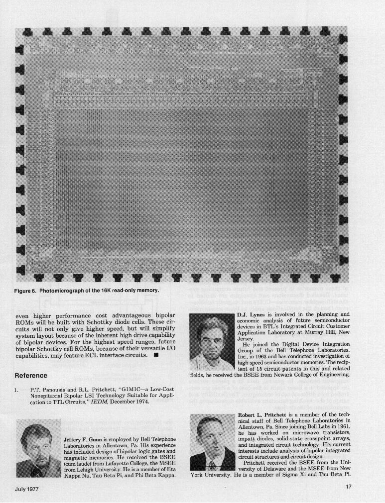
Figure 6. Photomicrograph of the 16K read-only memory.
even higher performance cost advantageous bipolarROMs will be built with Schottky diode cells. These cir-cuits will not only give higher speed, but will simplifysystem layout because of the inherent high drive capabilityof bipolar devices. For the highest speed ranges, futurebipolar Schottky cell ROMs, because of their versatile I/Ocapabilities, may feature ECL interface circuits. U
Reference
D.J. Lynes is involved in the planning andeconomic analysis of future semiconductordevices in BTL's Integrated Circuit CustomerApplication Laboratory at Murray Hill, New
_ I _ ~~Jersey.He joined the Digital Device Integration
Group of the BeU Telephone Laboratories,Inc., in 1963 and has conducted investigation ofhigh-speed semiconductor memories. The recip-iient of 15 circuit patents in this and related
fields, he received the BSEE from Newark College of Engineering.
1. P.T. Panousis and R.L. Pritchett, "GIMIC-a Low-CostNonepitaxial Bipolar LSI Technology Suitable for Appli-cation to TTL Circuits," IEDM, December 1974.
Jeffery F. Gunn is employed by Bell TelephoneLaboratories in Allentown, Pa. His experiencehas included design of bipolar logic gates andmagnetic memories. He received the BSEE(cum laude) from Lafayette College, the MSEEfrom Lehigh University. He is a member of EtaKappa Nu, Tau Beta Pi, and Phi Beta Kappa.
Robert L. Pritchett is a member of the tech-rnical staff of Bell Telephone Laboratories inAllentown, Pa. Since joining Bell Labs in 1961,he has worked on microwave transistors,impatt diodes, solid-state crosspoint arrays,and integrated circuit technology. His currentinterests include analysis of bipolar integratedcircuit structures and circuit design.
Pritchett received the BSEE from the Uni-versity of Delaware and the MSEE from New
York University. He is a member of Sigma Xi and Tau Beta Pi.
17July 1977