Embed Size (px)
Citation preview
ABSTRACT
HARDWARE IMPLEMENTATION OF HEVC INVERSE TRANSFORM
The High Efficiency Video Coding (HEVC) standard relies on the use of the inverse
discrete cosine transform (IDCT) to perform video decompression. During encoding, the
transform takes residual data and transforms it from the spatial domain to the frequency domain.
This frequency domain representation can then be compressed, using quantization, while still
retaining a high level of video quality when decoded and presented to the user. HEVC has
increased the complexity of the decoder and the inverse transform lends itself well to hardware
acceleration due to repeated addition and multiplication on unit blocks. With 4K video
emerging as the successor to HD, hardware implementations will be critical to the performance
of real time video applications. A hardware implementation of the inverse quantization and
inverse transform, compliant to the HEVC standard, will be presented. The design targets the
4x4 inverse quantization and transform, synthesis, and place & route using the Nangate
FreePDK45 Open Cell Library. An analysis of speed, area, and throughput will be presented
and compared to similar ASIC designs. The operational frequency of this design will support 4K
video at up to 30 frames/sec. The core area of this design takes up 14664 µm2 and can operate
at max. frequency of 367 MHz.
Richard Calusdian
May 2019


HARDWARE IMPLEMENTATION OF HEVC INVERSE TRANSFORM
by
Richard Calusdian
A thesis
submitted in partial
fulfillment of the requirements for the degree of
Master of Science in Engineering, Electrical Engineering Option
in the Lyles College of Engineering
California State University, Fresno
May 2019
APPROVED
For the Department of Electrical and Computer Engineering:
We, the undersigned, certify that the thesis of the following student meets the required standards of scholarship, format, and style of the university and the student's graduate degree program for the awarding of the master's degree. Richard Calusdian
Thesis Author
Aaron Stillmaker (Chair) Electrical and Computer Engineering
Reza Raeisi Electrical and Computer Engineering
Hovannes Kulhandjian Electrical and Computer Engineering
For the University Graduate Committee:
Dean, Division of Graduate Studies

AUTHORIZATION FOR REPRODUCTION
OF MASTER’S THESIS
Yes I grant permission for the reproduction of this thesis in part or in its entirety without further authorization from me, on the condition that the person or agency requesting reproduction absorbs the cost and provides proper acknowledgment of authorship.
Permission to reproduce this thesis in part or in its entirety must be
obtained from me.
Signature of thesis author:

ACKNOWLEDGMENTS
It has been a long journey for me. I was an undergraduate student here quite a few years
ago and can remember that the thought of pursuing a graduate degree was far from my thoughts.
While working at Pelco by Schneider Electric, I was given the opportunity to attend graduate
school and so I enrolled in my first graduate class after a long absence from the halls of the Lyles
Building.
Working at Pelco I was given much flexibility in my schedule and to that I must thank
my supervisor at that time, Mr. Mark Kawakami, for his support and encouragement.
The first graduate class I attended was taught by a familiar face and one that I have
admired since I was an undergraduate student. I would like to thank Dr. Daniel Bukofzer for his
always present energy and enthusiasm for his students and his teaching.
Continuing on, I must thank Dr. Aaron Stillmaker, without whom I very likely would not
be writing these words. His guidance, patience, and enthusiasm for the work I was undertaking
are greatly appreciated. I also want to thank the thesis panel members, Dr. Reza Raeisi and Dr.
Hovannes Kulhandjian, who so graciously accepted my invitation even with their very full
schedules.
Lastly, I would like to thank my family. My brother who attended as an undergraduate
himself, paved the way for his younger sibling. I must thank my wife, who encouraged me at
just the right moments and my amazing parents who gave me the opportunity to attend an
institution of higher learning at the very beginning of this long journey.

TABLE OF CONTENTS Page
LIST OF TABLES ............................................................................................................ vii
LIST OF FIGURES ......................................................................................................... viii
1. INTRODUCTION ........................................................................................................... 1
1.1 Video Compression Standards ............................................................................... 1
1.2 Encoder Tools and Techniques .............................................................................. 3
2. RELATED WORK .......................................................................................................... 8
2.1 Inverse Transform Designs .................................................................................... 8
3. BACKGROUND WORK .............................................................................................. 10
3.1 Signed Arithmetic ................................................................................................ 10
3.2 Memory Architecture .......................................................................................... 11
3.3 Codec and ME Engine ......................................................................................... 13
4. DESIGN ......................................................................................................................... 15
4.1 RTL Design ......................................................................................................... 16
4.2 Simulation ............................................................................................................ 22
4.3 Synthesis .............................................................................................................. 23
4.4 Place and Route ................................................................................................... 25
5. RESULTS ...................................................................................................................... 39
6. CONCLUSION ............................................................................................................. 42
REFERENCES .................................................................................................................. 44
APPENDICES ................................................................................................................... 47
APPENDIX A: VERILOG FILES .................................................................................... 48
APPENDIX B: VERILOG TESTBENCH ........................................................................ 59
APPENDIX C: MATLAB FILES ..................................................................................... 64
APPENDIX D: SYNTHESIS TCL FILE .......................................................................... 68

vi
APPENDIX E: PLACE & ROUTE COMMANDS .......................................................... 72
APPENDIX F: VERIFICATION REPORTS .................................................................... 74
APPENDIX G: HOLD TIMING SUMMARY ................................................................. 76

LIST OF TABLES
Page
Table 1. Signed features used in RTL code ....................................................................... 11
Table 2. Floorplan Parameters ........................................................................................... 27
Table 3. Architecture and Performance Comparison ........................................................ 40
LIST OF FIGURES
Page
Figure 1. HEVC encoder-decoder signal path [21] ............................................................. 2
Figure 2. 2D DCT of 4x4 block of constant values ............................................................. 5
Figure 3. Zig-zag pattern of entropy encoding .................................................................... 7
Figure 4. Example of casting and signed value ................................................................. 11
Figure 5. Transpose cell design ......................................................................................... 13
Figure 6. Block diagram of proposed design ..................................................................... 15
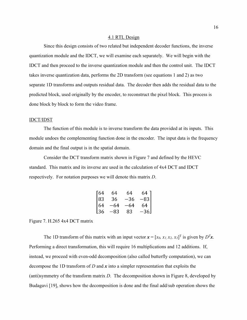
Figure 7. H.265 4x4 DCT matrix ...................................................................................... 16
Figure 8. Even-odd decomposition for 1D IDCT .............................................................. 17
Figure 9. H.265 4x4 DST matrix ....................................................................................... 17
Figure 10. Two stage IDCT showing scaling [8] .............................................................. 19
Figure 11. State machine from control module ................................................................. 21
Figure 12. Simulation showing writing to ram module in dequantizer ............................. 22
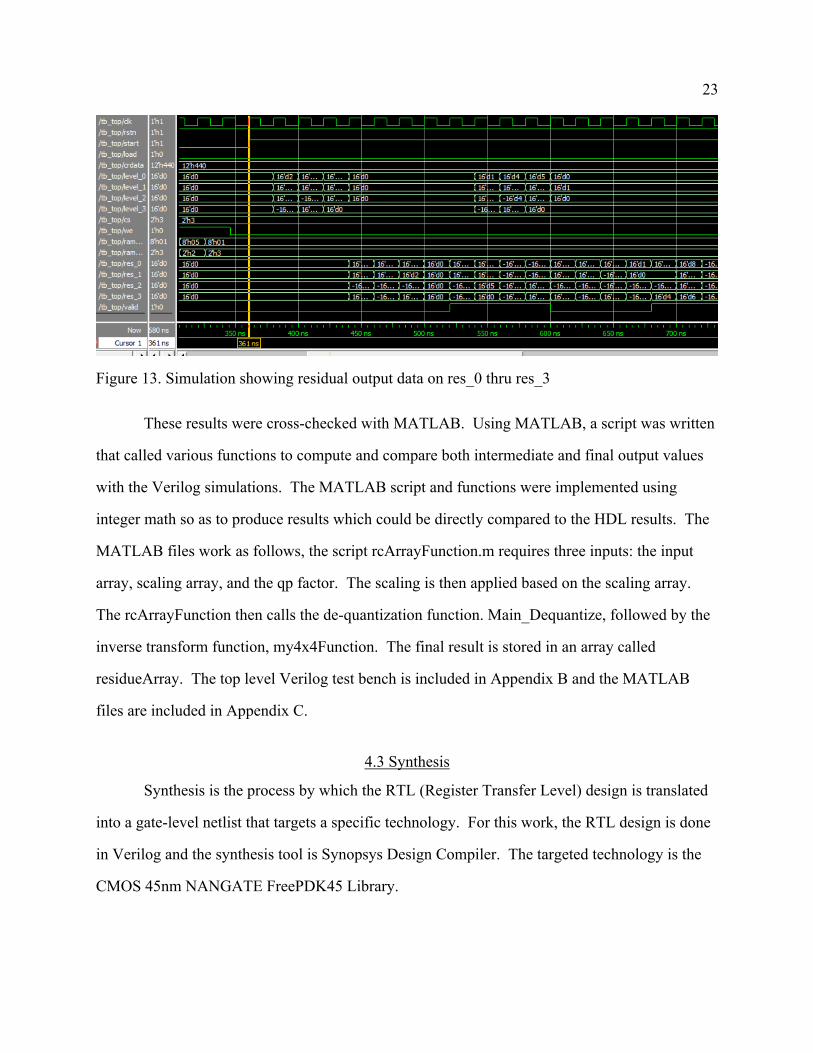
Figure 13. Simulation showing residual output data on res_0 thru res_3 ......................... 23
Figure 14. Area, synthesis results ...................................................................................... 24
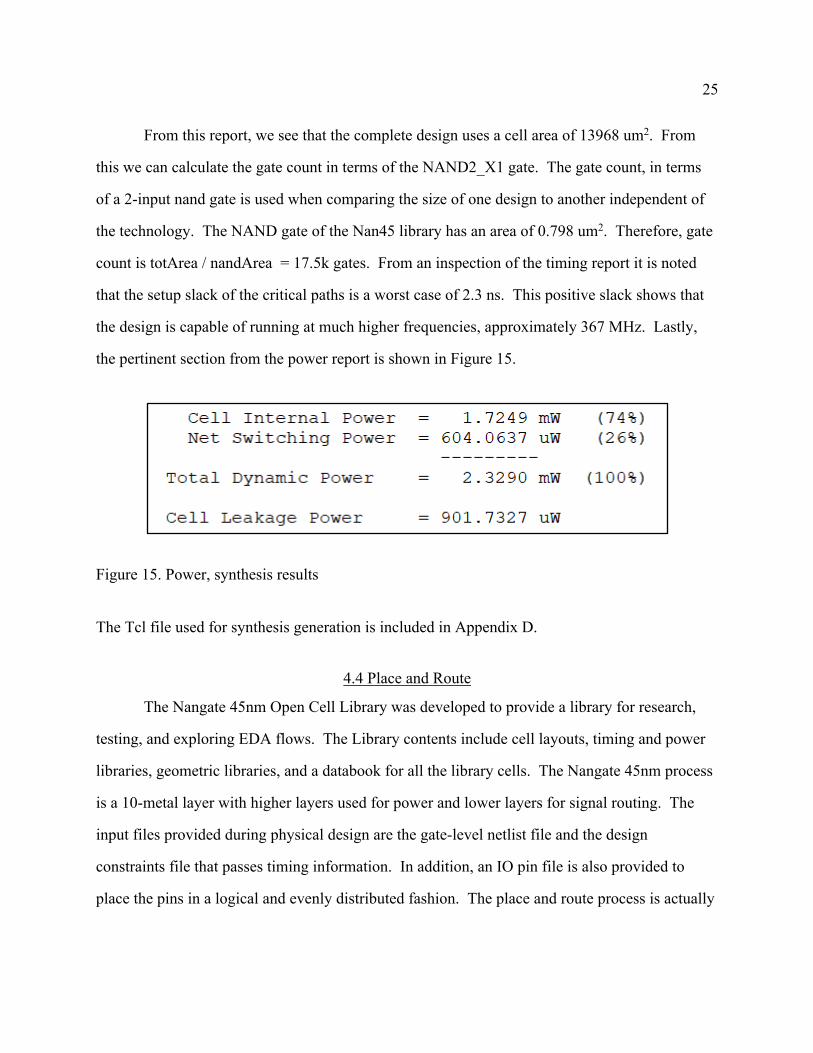
Figure 15. Power, synthesis results ................................................................................... 25
Figure 16. Power network ................................................................................................. 29
Figure 17. Cell placement with 0.95 core utilization ........................................................ 31
Figure 18. Zoomed in view of section of cell placement .................................................. 32
Figure 19. Clock tree ......................................................................................................... 33
Figure 20. Example of clock buffer insertion .................................................................... 34
Figure 21. Map of setup margin ........................................................................................ 35
Figure 22. Map of hold margin .......................................................................................... 36
Figure 23. Complete design ............................................................................................... 37

1. INTRODUCTION
1.1 Video Compression Standards
One of the most widely adopted video compression standards today [1], is the
H.264/MPEG-AVC standard [2], commonly referred to as H.264. Its goal, when initially
conceived, was to provide a compression method that provided bit rates approximately halved
from previous standards such as H.263 and MPEG-4 (part 2) while still providing good
video [3]. The H.264 standard was the work of an international group, the Joint Collaborative
Team on Video Coding (JCT-VC), consisting of the ITU-T Video Coding Experts Group and
ISO/IEC Moving Picture Experts Group. The standard was released in 2003.
The same group that released H.264 has also recently developed a follow-up, the
H.265/MPEG-HEVC standard [4], which is commonly referred to as H.265 or HEVC. This
latest standard builds on the framework of H.264 and expands and extends the tools and features
of the standard. It was the goal of the JCT-VC to develop a standard that improved upon the
existing coding efficiency while specifically addressing the needs of the proliferation of HD
video and UHD while also adding significant support for parallel processing architectures [1].
The HEVC/H.265 standard was released in 2013.
In order to effectively compress digital video, HEVC and H.264 use similar tools and
processes to produce an efficient bitstream. The input video frames are first partitioned into
smaller blocks in preparation for predictive encoding. Each of these blocks is then encoded
using a block that is in the same frame or in another frame that has been previously encoded and
transmitted.
2
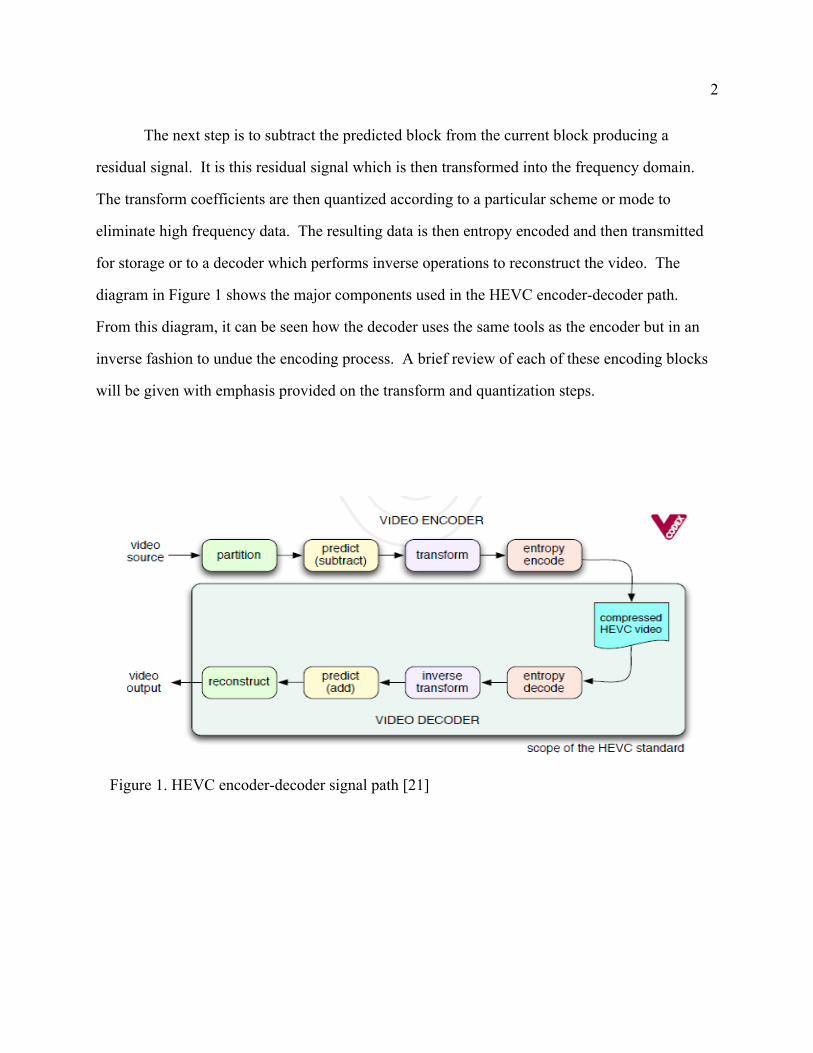
The next step is to subtract the predicted block from the current block producing a
residual signal. It is this residual signal which is then transformed into the frequency domain.
The transform coefficients are then quantized according to a particular scheme or mode to
eliminate high frequency data. The resulting data is then entropy encoded and then transmitted
for storage or to a decoder which performs inverse operations to reconstruct the video. The
diagram in Figure 1 shows the major components used in the HEVC encoder-decoder path.
From this diagram, it can be seen how the decoder uses the same tools as the encoder but in an
inverse fashion to undue the encoding process. A brief review of each of these encoding blocks
will be given with emphasis provided on the transform and quantization steps.
Figure 1. HEVC encoder-decoder signal path [21]
3
1.2 Encoder Tools and Techniques
Frame Partitioning
In order to process a video sequence, each frame of the sequence is partitioned into non-
overlapping square blocks of pixels. The actual dimensions of the primary block size vary from
the HEVC and H.264 standards, however the concept is similar. These primary blocks can then
be sub-divided further down into smaller blocks, called coding blocks, for eventual spatial or
temporal coding. Simply put, the encoder algorithm will encode large blocks where possible to
reduce the bit rate and leave the small blocks only where needed to retain detail. The H.264
standard calls its primary block a macroblock and is of size 16x16 pixels, whereas HEVC uses
the CTU, which can be as small as 16x16 and as large as 64x64. In all cases these initial blocks
may be recursively reduced in size to make coding decisions, e.g. intra vs inter. An advantage of
the larger block size of 32x32 or 64x64, is that for large flat areas, the HEVC standard can offer
better efficiency as compared to the smaller 16x16 macroblock of H.264 [1].
Intra-Frame Prediction
The very first frame in a sequence will always rely solely on redundancy within the frame
and a frame solely using this prediction mode is termed an I-frame. This type of prediction takes
advantage of the spatial redundancy within a frame of video and this redundancy can be
exploited to help compress the video. H.264 provides for up to nine intra prediction modes [5],
whereas HEVC supports up to 35 intra prediction modes [1]. The intra mode which minimizes
some metric, such as Sum of Absolute Differences, SAD, is used to determine which mode will
be used on the current block. This information is sent in the bitstream where it is received by the
decoder for reconstruction of the picture signal.

4
Inter-Frame Prediction & Sub-Pixel Compensation
In addition to the I-frames mentioned earlier there are also Predictive or P-frames which
use redundancy from one or more previous frames, and Bidirectional or B-frames which use
redundancy from both previous and future frames.
Just as neighboring pixels within a frame show similarity, so also do neighboring
frames [6]. This temporal redundancy is reliant on having stored reference frames to use in
finding candidate blocks to compare to the original. A metric, for example SAD, is then used to
determine which candidate block gives the smallest error. A motion vector, which provides the
location of the prediction block, is then inserted into the bitstream.
The simplest realization of motion vector accuracy would be to limit vectors to integer
deltas of the picture grid, however, it is often the case that the best candidate will not reside on
an integer delta of the grid. Interpolation of sub-pixel candidates is done using interpolation
filters. The use of sub-pixel motion vector accuracy allows for better motion estimation.
Transform
Similar to previous video compression standards, HEVC defines a 2D transform for sizes
4x4, 8x8, 16x16, and 32x32. The transform is used to change the representation of the residual
signal from the spatial domain to the frequency domain. In HEVC this is accomplished by using
a finite approximation to the discrete cosine transform (DCT). HEVC explicitly defines the
matrix values of the DCT as integer values to make the math more amenable to digital systems
and to produce consistent results. Also, the integer values avoid encoder/decoder mismatches
due to differing precision of representations of the DCT matrix values. The equations for the
HEVC DCT and IDCT for an input residual block U and transform matrix D are shown in (1)
and (2). One thing to note is that the transform is a lossless operation.
5
!"#(%) = ! ∗ % ∗ !) = * (1)
+!"#(*) = !) ∗ * ∗ ! = % (2)
In actual implementation the inverse transform is computed by separating the equation in
(2) into two one-dimensional transformations in succession. This will be discussed further in
Chapter 4. Once the DCT is performed, the coefficients of the resulting matrix represent
increasing frequency components of the image, starting with a DC coefficient in the upper-left
corner and increasing as we move down and to either side, with the highest frequency component
in the lower-right corner. Consider the case of a flat residual block, such that the residual block
has all entries equal the same value. After transformation, such a block will yield a set of
coefficients with only one non-zero element as show in Figure 2. The interpretation of this
follows from the fact that the coefficients arranged with the lowest frequency term positioned in
the upper left corner and increasing frequencies are placed below and to the right as we move
away from this term. The highest frequency is thus positioned at the lower right corner.
In the resulting transformed block, the upper-left corner term is called the DC coefficient
and represents the average value of the residual block of pixels. It tends to be the case that video
has most of its energy in the lower frequency components, and interestingly, the human eye is
not sensitive to high frequency contrasts. Both of these facts, allow video to be compressed by
Figure 2. 2D DCT of 4x4 block of constant values
6
discarding the higher frequency content with little loss of detail as perceived by the human
eye [7].
Quantization
The transformation of the video signal into frequency components is key to video
compression. Once transformed, the resulting coefficients are quantized by dividing them by an
integer and rounding down. The divisor is called the quantization step and is derived from the
encoded parameter, quantization parameter (QP). As a result of the division and rounding, some
coefficients will be rounded down to zero. For larger values of the quantization step, more
zeroes will be produced in the quantized block. Typically, the higher frequency components
have less energy to begin with and dividing them down, further reduces their values. The larger
this divisor, the more coefficients are thrown away and more compression is achieved at the cost
of picture detail in the reconstructed picture. This process of quantization is a lossy step since
data is being thrown away, and provided only the higher frequency components are removed, the
resulting picture will appear to be as detailed as the original, to the observer. The previous
standard, H.264, exclusively relies on DCT, but in the case of HEVC, the use of the DCT is
augmented by use of the DST for 4x4 luma intra-prediction blocks [4]. From research, it was
found that using the DST on luma intra-prediction blocks improved the bitsream compression by
about 1% [8].
7
Entropy Encoding
Finally, the resulting bitstream undergoes entropy encoding to further reduce the bit rate.
Entropy encoding compresses the data by encoding frequently occurring symbols with shorter
length symbols and reserving longer length symbols for those input symbols that occur less
frequently. If we consider the case of a 4x4 block as shown in Figure 3, the encoding process
will encode in a zig-zag pattern. This zig-zag pattern will find, with quantization, runs of zeroes
as we move from the upper left corner to the lower right corner. This grouping of zeroes will
allow for efficient compression with the use of shorter symbol words. Typically, a Huffman
coding or Arithmetic coding method is used for compressing the HEVC bitstream that may then
be stored or transmitted.
The remainder of this paper is organized as follows. Chapter 2 discusses previous work
on the IDCT transform. Chapter 3 provides background research done to prepare for the design.
Chapter 4 provides information on the design of the inverse quantization and IDCT. Chapter 5
compares the results of the design to other works and Chapter 6 provides concluding remarks
and some thoughts on follow-on work.
Figure 3. Zig-zag pattern of entropy encoding

2. RELATED WORK
2.1 Inverse Transform Designs
In the work done by Ma [9], a unique approach to the IDCT is proposed involving
decomposing the matrix into sub-matrices. As has been done by many works, the authors exploit
the (anti)symmetry property of the DCT matrix, however Ma continues the decomposition into
multiple factors using sparse matrices to significantly reduce the number of multiplications and
additions when compared to the direct method. The design was done using combinational
circuits only, thus no clock frequency is provided. The design also appears to use two IDCT
blocks which will negatively affect circuit area and power.
In one of the most unique approaches, Porto [10], proposes a fast 4-point IDCT that uses
statistical information of the transformed residual data. Their analysis found that for large values
of QP, a very high percentages of the input columns consist of a non-zero term in the top
position and all other terms equal to zero. For this special case, the 4-point IDCT simplifies to
setting all four values to one-half the value of the top coefficient. Further analysis by Porto
found that if the first 1-D transform treats all input columns as a special case followed by a
second regular 1-D transform, that the cost to quality is maintained per the PSNR measurement
along with a small but desirable decrease in bit rate. The benefits of using this approach are
reduced circuit complexity and high pixel throughput. The PSNR parameter used to assess
quality is one accepted measurement but research is still on-going looking for objective metrics
to better reflect human perception of video quality [11]. Also, low QP values were not tested nor
were larger transforms which statistically may or may not be similar to the 4x4 blocks.
In the work done by Ziyou [12], the IDCT is again tackled by splitting the 2D transform
into two 1D transforms. However, instead of using a decomposition approach, Ziyou exploits
the (anti)symmetry exhibited by the HEVC transform matrix to minimize the physical quantity
of multipliers. Each multiplier is then reduced to a series of shifts and additions, reducing the
complexity of the multipliers. With this in mind, the design then proceeds by inputting only one

9
transformed pixel sample at a time. Each sample is then multiplied, in parallel, with every
matrix coefficient required to produce the 1D transform outputs dependent on the particular
input. This continues cycle by cycle, for every input block. What this means, is that to compute
the 1D 4-point transform would require 4 cycles and for an 8-point would require 8 clocks, etc.
In order to process one pixel per cycle, the design doubles the transpose memory and IDCT
engine count. While the bit count for the transpose memory is 2x what a typical shared IDCT
design uses, the gate count for the Ziyou design is smaller than most. The Ziyou design does
have a significant requirement that the clock frequency must operate at the pixel rate of the video
input.
3. BACKGROUND WORK
Prior to beginning the RTL design, there were a number of questions that remained
regarding how to design certain aspects of the inverse transform. In this section a discussion of
preliminary work will be presented and discussed.
3.1 Signed Arithmetic
The video data encountered in many applications is typically represented by 8-bit data
samples. The HEVC standard was initially released with support for 8-bit data only and this
work supports that bit depth. The 8-bit data samples range from 0-255 and are thus non-negative
values. Once this residual pixel data undergoes transformation, it is no longer made up solely of
non-negative numbers. Therefore, the data arriving at the inputs to this work’s module will
consist of negative and positive numbers. Accounting for these signed numbers during math
operations would appear to be an arduous task. Fortunately, Verilog introduced a set of new data
types to address signed number math in 2001 [13]. However, with the use of these new types
also comes pitfalls and complications. It is the user’s responsibility to understand the
complexities associated with the signed data types.
In this work, a number of math operations are repeatedly performed on the input data. In
order to effectively perform these operations, it is critical that data types be declared as signed
when first created. A potential pitfall to be aware of, if an operand involved in an expression is
unsigned then the operation is also considered to be unsigned. In addition to the signed data
type, the 2001 version of Verilog also introduced two new signed shift operators. These new
shift operator sign extend the operand, thus preserving both the sign and the size of the operand.
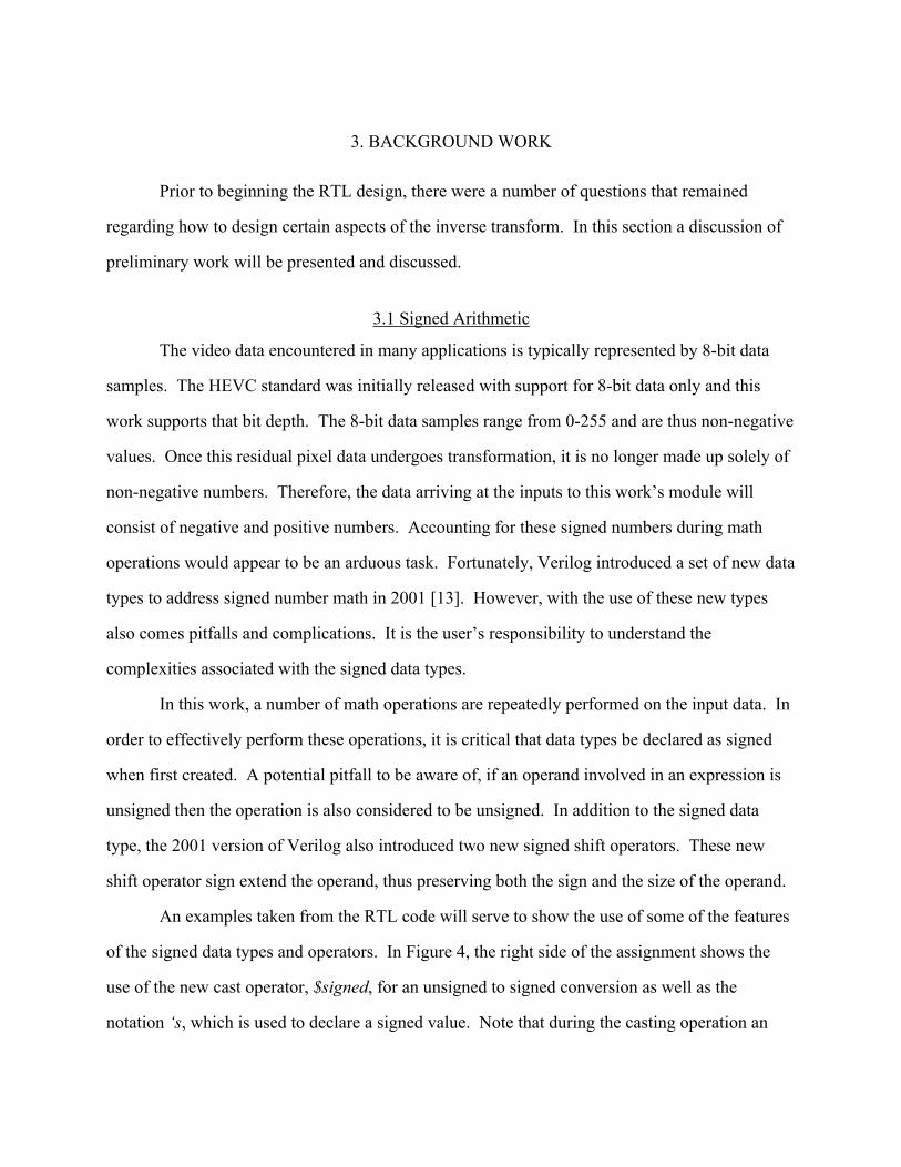
An examples taken from the RTL code will serve to show the use of some of the features
of the signed data types and operators. In Figure 4, the right side of the assignment shows the
use of the new cast operator, $signed, for an unsigned to signed conversion as well as the
notation ‘s, which is used to declare a signed value. Note that during the casting operation an
11
additional bit was inserted on the left side of the input signal. This is actually not required but
used to eliminate some warnings during synthesis.
Figure 4. Example of casting and signed value
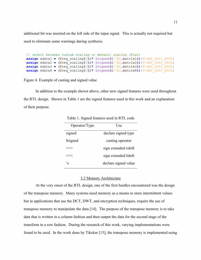
In addition to the example shown above, other new signed features were used throughout
the RTL design. Shown in Table 1 are the signed features used in this work and an explanation
of their purpose.
Table 1. Signed features used in RTL code
Operator/Type Use
signed declare signed type
$signed casting operator
>>> sign extended rshift
<<< sign extended lshift
‘s declare signed value
3.2 Memory Architecture
At the very onset of the RTL design, one of the first hurdles encountered was the design
of the transpose memory. Many systems need memory as a means to store intermittent values
but in applications that use the DCT, DWT, and encryption techniques, require the use of
transpose memory to manipulate the data [14]. The purpose of the transpose memory is to take
data that is written in a column fashion and then output the data for the second stage of the
transform in a row fashion. During the research of this work, varying implementations were
found to be used. In the work done by Tikekar [15], the transpose memory is implemented using
12
parallel banks which allow for writing a column into one bank location and reading a row from a
different bank location. This would be very useful when processing different size transform
blocks. The SRAM memory is area efficient but comes with the overhead of row/column
decoding, sense amp, etc. needed for SRAM. In the work proposed by Hsia [16], a shift-register
based design with custom VLSI circuitry is employed. The custom design allows for smaller
size flip-flops and reduced power. This design achieves a quoted max frequency of 120 MHz in
0.35 um technology. This max frequency is a bit lower than that required for real-time video
processing done in this work, it should be noted that using 45nm technology could improve the
quoted frequency.
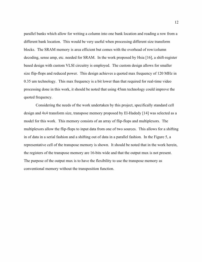
Considering the needs of the work undertaken by this project, specifically standard cell
design and 4x4 transform size, transpose memory proposed by El-Hadedy [14] was selected as a
model for this work. This memory consists of an array of flip-flops and multiplexors. The
multiplexors allow the flip-flops to input data from one of two sources. This allows for a shifting
in of data in a serial fashion and a shifting out of data in a parallel fashion. In the Figure 5, a
representative cell of the transpose memory is shown. It should be noted that in the work herein,
the registers of the transpose memory are 16-bits wide and that the output mux is not present.
The purpose of the output mux is to have the flexibility to use the transpose memory as
conventional memory without the transposition function.

13
Figure 5. Transpose cell design
One additional comment to make about data width sizes regards the use of 16-bit wide
register and memory. The HEVC standard specified 16-bit wide memory and operands for input
into the inverse transform. This, however, would result in erroneous intermittent calculations
during the inverse transform arithmetic. For example, when multiplying any two binary
numbers, the resulting product may be up to twice as wide as the individual operands. An
analysis done by the JCT-VC on the range requirements for HEVC inverse transform
operations [17], was used as the guide for setting bit widths for the inverse transform engine.
Specifically, for this work, a width of 24 bits is required prior to any shifting operations. After
shifting, as specified by the HEVC standard, the results may be stored in 16-bit registers.
3.3 Codec and ME Engine
A review of complete HEVC encoders as well as a motion estimation engine was also
performed in order gain some understanding of how the entire encoder functions as well as the
integration of a sub-module within a larger encoder design.
In the work done by Pastuszak [6], an intra encoder that can support 4K video at 30
frames/sec is proposed. The proposed encoder also employs Rate Distortion Optimization,
RDO, to determine the best coding mode to use on segmented blocks. The RDO is a process by

14
which every coding decision can benefit from a distortion and bit-rate analysis. This process is
computationally intensive since in order to make the most accurate decision on coding mode,
every block of pixels would need to be evaluated against all possible coding modes, transformed,
and entropy encoded. At this point the bit-rate cost and distortion could then be evaluated to
determine the coding mode that minimizes distortion while also keeping the bit-rate below a
threshold. This computation would negate support for realtime use as elaborated by Pastuszak.
The encoder uses a simplified RDO process that leaves out inter coding and pre-selects a
smaller set intra modes in order to reduce the sheer number of calculations that must be
evaluated. Another simplification is relying on a table of values used to estimate the bit-rate cost
of coding modes as opposed to performing actual entropy encoding.
Another sub-module that was reviewed is the motion estimator accelerator done by
Braly [18]. This motion estimator targets realtime 4K video encoding in a multicore platform,
AsAP. The motion estimator is a sub-module within the encoder that is used to determine the
best inter coding mode based on a distortion calculation, in this case, SAD. The motion
estimator supports all 35 inter modes and block sizes as defined by the HEVC standard. The
work was entered in Verilog RTL, modeled using Matlab, and placed and routed using standard
cell techniques. The HEVC standard has introduced a new structure called slices. These are
structures that can be decoded independently of other slices in the same picture [1]. These
structures are meant to support parallel processing platforms. It may be that the AsAP could be a
platform well suited for video compression.
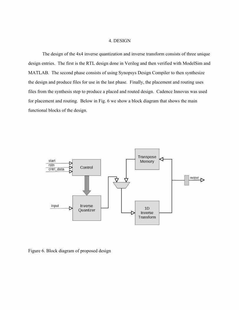
4. DESIGN
The design of the 4x4 inverse quantization and inverse transform consists of three unique
design entries. The first is the RTL design done in Verilog and then verified with ModelSim and
MATLAB. The second phase consists of using Synopsys Design Compiler to then synthesize
the design and produce files for use in the last phase. Finally, the placement and routing uses
files from the synthesis step to produce a placed and routed design. Cadence Innovus was used
for placement and routing. Below in Fig. 6 we show a block diagram that shows the main
functional blocks of the design.
Figure 6. Block diagram of proposed design
16
4.1 RTL Design
Since this design consists of two related but independent decoder functions, the inverse
quantization module and the IDCT, we will examine each separately. We will begin with the
IDCT and then proceed to the inverse quantization module and then the control unit. The IDCT
takes inverse quantization data, performs the 2D transform (see equations 1 and 2) as two
separate 1D transforms and outputs residual data. The decoder then adds the residual data to the
predicted block, used originally by the encoder, to reconstruct the pixel block. This process is
done block by block to form the video frame.
IDCT/IDST
The function of this module is to inverse transform the data provided at its inputs. This
module undoes the complementing function done in the encoder. The input data is the frequency
domain and the final output is in the spatial domain.
Consider the DCT transform matrix shown in Figure 7 and defined by the HEVC
standard. This matrix and its inverse are used in the calculation of 4x4 DCT and IDCT
respectively. For notation purposes we will denote this matrix D.
The 1D transform of this matrix with an input vector x = [x0, x1, x2, x3]T is given by DTx.
Performing a direct transformation, this will require 16 multiplications and 12 additions. If,
instead, we proceed with even-odd decomposition (also called butterfly computation), we can
decompose the 1D transform of D and x into a simpler representation that exploits the
(anti)symmetry of the transform matrix D. The decomposition shown in Figure 8, developed by
Budagavi [19], shows how the decomposition is done and the final add/sub operation shows the
Figure 7. H.265 4x4 DCT matrix

17
output y which represents the 1D inverse transform result. From the equations for y, it can be
observed that even-odd decomposition needs only six multiplications and eight additions. To
compute the 2D transform will require 48 multiplications and 64 additions versus 128
multiplications and 96 additions for the direct method.
Figure 8. Even-odd decomposition for 1D IDCT
The development shown in Figure 8 is dependent on the matrix exhibiting
(anti)symmetry properties. The DST matrix does not have these properties but some savings in
multiplications and additions can still be achieved. By computing the equations for the direct
method, it may be observed that certain patterns emerge in the resulting sums. The DST matrix
is shown Figure 9. Note that the IDST matrix is simply the transpose of the DST.
Figure 9. H.265 4x4 DST matrix

18
Observe that the term 84 is the sum of (29 + 55) and that there are many repeated terms
in the matrix. By performing a direct 1D transform and taking the above observations into
account, we can be used to reduce the number of multiplications and additions. If we pre-assign
common sums and one product as shown collectively in (3), then the equations for the output
vector y may be simplified as shown in (4) and (5). This reduction was taken from the Kvazaar
HEVC encoder project [20].
,0 = .0 + .2,1 = .2 + .3,2 = .0 − .3,3 = 74 ∗ .1 (3)
70 = 29 ∗ ,0 + 55 ∗ ,1 + ,371 = 55 ∗ ,2 − 29 ∗ ,1 + ,3 (4)
72 = 74 ∗ (.0 − .2 + .3)73 = 55 ∗ ,0 + 29 ∗ ,2 − ,3 (5)
Using this approach, we can reduce the operations to eight multiplications and 11
additions versus 16 multiplications and 12 additions for the direct method.
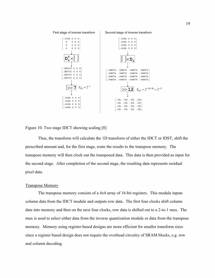
The HEVC standard also requires scaling of the output data after each 1D transform
stage. This scaling serves both to maintain the norm through the transform process and also to
scale the resultant data to 16 bits wide, including the sign bit. The choice of 16 bits was made as
a trade-off between accuracy and implementation costs [4], [8]. The Figure 10 from Sze, shows
the two stages of the inverse transform and the intermediate scaling for video with 8-bit depth.
19
Figure 10. Two stage IDCT showing scaling [8]
Thus, the transform will calculate the 1D transform of either the IDCT or IDST, shift the
prescribed amount and, for the first stage, route the results to the transpose memory. The
transpose memory will then clock out the transposed data. This data is then provided as input for
the second stage. After completion of the second stage, the resulting data represents residual
pixel data.
Transpose Memory
The transpose memory consists of a 4x4 array of 16-bit registers. This module inputs
column data from the IDCT module and outputs row data. The first four clocks shift column
data into memory and then on the next four clocks, row data is shifted out to a 2-to-1 mux. The
mux is used to select either data from the inverse quantization module or data from the transpose
memory. Memory using register-based designs are more efficient for smaller transform sizes
since a register based design does not require the overhead circuitry of SRAM blocks, e.g. row
and column decoding.
20
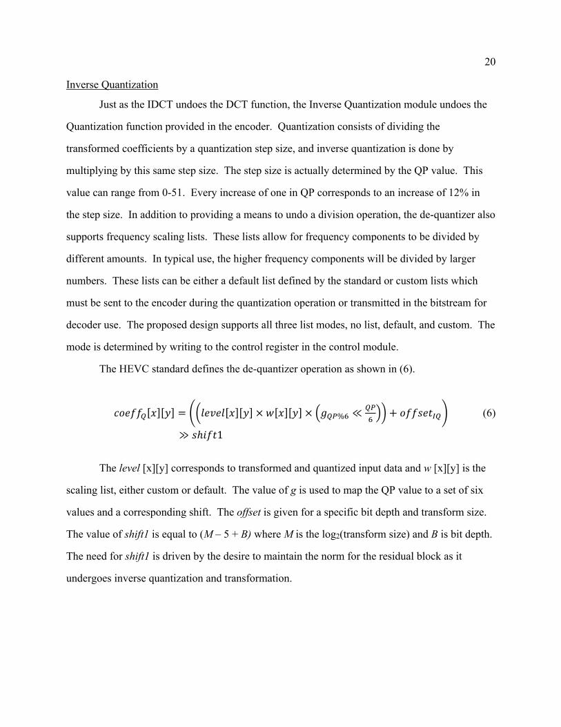
Inverse Quantization
Just as the IDCT undoes the DCT function, the Inverse Quantization module undoes the
Quantization function provided in the encoder. Quantization consists of dividing the
transformed coefficients by a quantization step size, and inverse quantization is done by
multiplying by this same step size. The step size is actually determined by the QP value. This
value can range from 0-51. Every increase of one in QP corresponds to an increase of 12% in
the step size. In addition to providing a means to undo a division operation, the de-quantizer also
supports frequency scaling lists. These lists allow for frequency components to be divided by
different amounts. In typical use, the higher frequency components will be divided by larger
numbers. These lists can be either a default list defined by the standard or custom lists which
must be sent to the encoder during the quantization operation or transmitted in the bitstream for
decoder use. The proposed design supports all three list modes, no list, default, and custom. The
mode is determined by writing to the control register in the control module.
The HEVC standard defines the de-quantizer operation as shown in (6).
,:;<<=[.][7] = @AB;C;B[.][7] × E[.][7] × FG=H%J ≪=H
JLM + :<<N;OP=Q (6)
≫ NℎT<O1
The level [x][y] corresponds to transformed and quantized input data and w [x][y] is the
scaling list, either custom or default. The value of g is used to map the QP value to a set of six
values and a corresponding shift. The offset is given for a specific bit depth and transform size.
The value of shift1 is equal to (M – 5 + B) where M is the log2(transform size) and B is bit depth.
The need for shift1 is driven by the desire to maintain the norm for the residual block as it
undergoes inverse quantization and transformation.
21
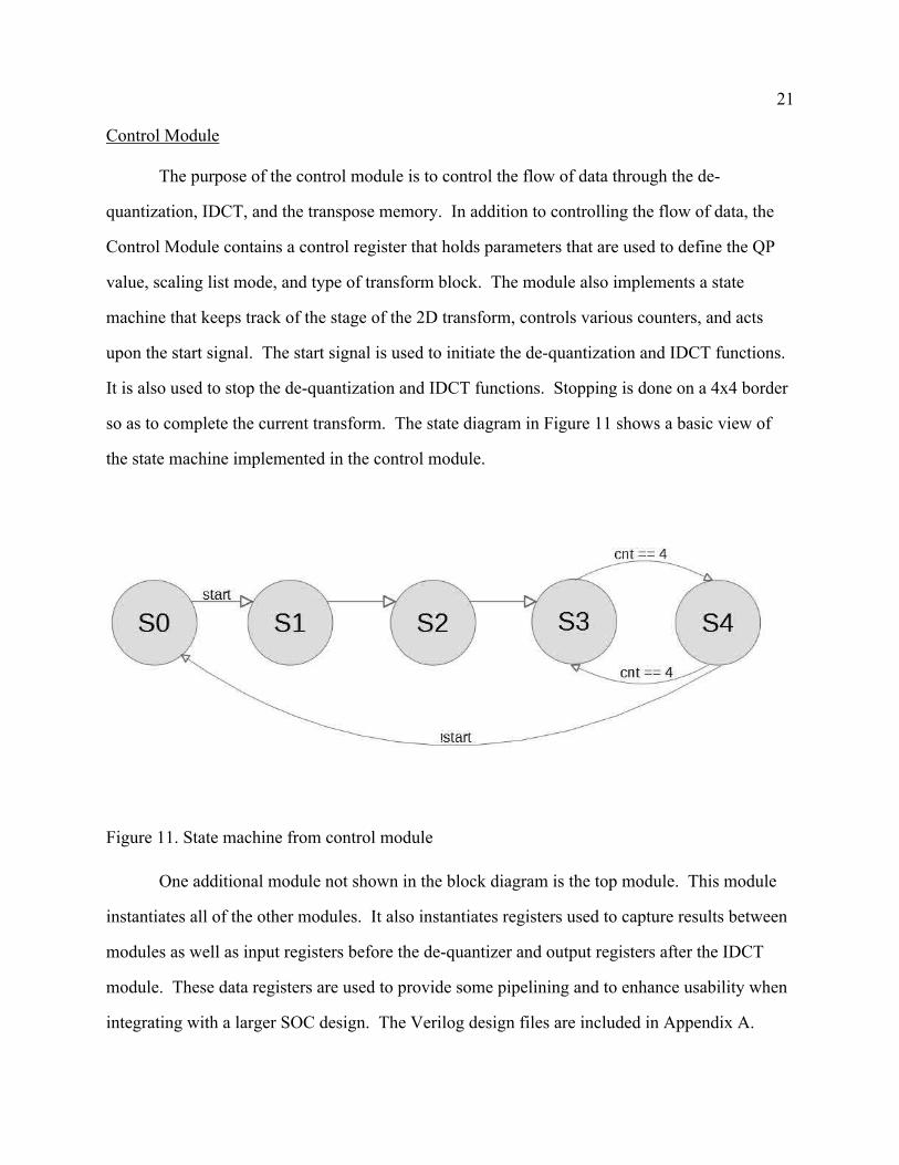
Control Module
The purpose of the control module is to control the flow of data through the de-
quantization, IDCT, and the transpose memory. In addition to controlling the flow of data, the
Control Module contains a control register that holds parameters that are used to define the QP
value, scaling list mode, and type of transform block. The module also implements a state
machine that keeps track of the stage of the 2D transform, controls various counters, and acts
upon the start signal. The start signal is used to initiate the de-quantization and IDCT functions.
It is also used to stop the de-quantization and IDCT functions. Stopping is done on a 4x4 border
so as to complete the current transform. The state diagram in Figure 11 shows a basic view of
the state machine implemented in the control module.
Figure 11. State machine from control module
One additional module not shown in the block diagram is the top module. This module
instantiates all of the other modules. It also instantiates registers used to capture results between
modules as well as input registers before the de-quantizer and output registers after the IDCT
module. These data registers are used to provide some pipelining and to enhance usability when
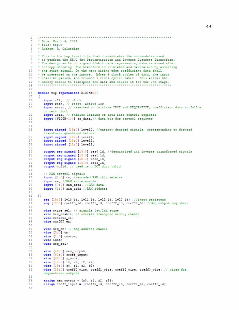
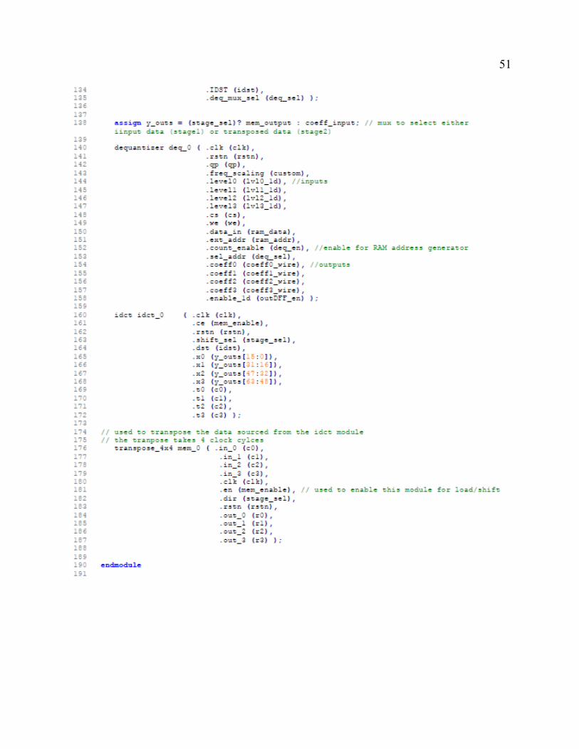
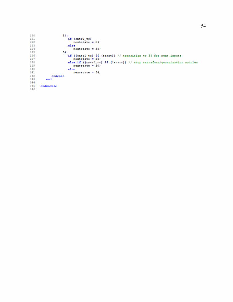
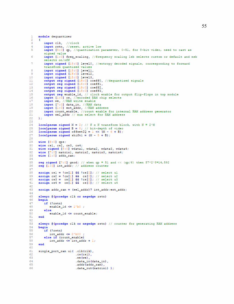
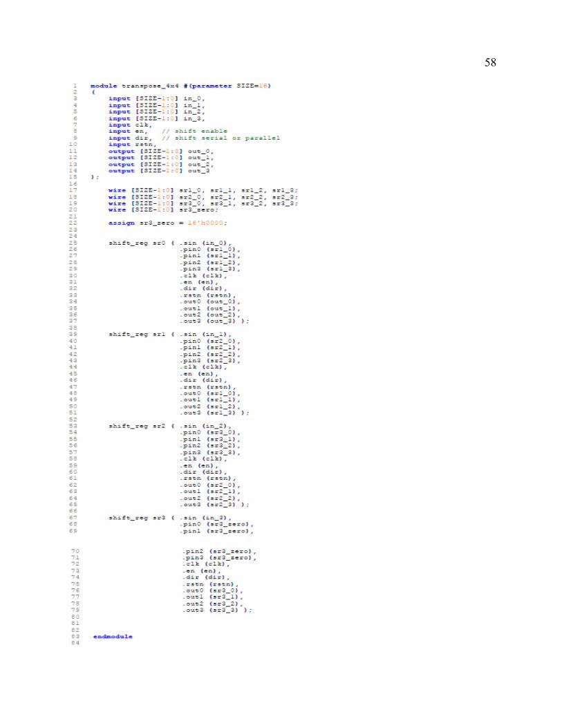
integrating with a larger SOC design. The Verilog design files are included in Appendix A.

22
4.2 Simulation
Each Verilog module has a corresponding test bench that was used to verify proper
functionality using ModelSim. A top level test bench was then used to instantiate all the
modules and test end to end. This top level test bench was then simulated to verify functionality
for various modes of operation including custom frequency scaling lists, QP values, and other
supported modes. The first step in processing 4x4 blocks is to configure the various parameters
of the inverse quantization and transform. This is done by writing to the control register, and if
enabled, writing to the ram module with a custom scaling list.
Figure 12. Simulation showing writing to ram module in dequantizer
In Figure 12, the custom scaling list is shown being written into RAM memory. These
stored values will then be used to scale the coefficient data on a one for one basis, provided the
control register is setup to use the scaling list. Thus, for a 4x4 inverse operation, sixteen values
are written into memory. The actual inverse quantization and transformation are initiated by
asserting the start signal high. In Figure 13 this assertion event is shown, along with the input
data being driven on the level_0-3 signals. The output data is shown on the res_0-3 signals and
represents the residual pixel data. The valid signal is also output and validates the data for a
succeeding decoding step.
23
Figure 13. Simulation showing residual output data on res_0 thru res_3
These results were cross-checked with MATLAB. Using MATLAB, a script was written
that called various functions to compute and compare both intermediate and final output values
with the Verilog simulations. The MATLAB script and functions were implemented using
integer math so as to produce results which could be directly compared to the HDL results. The
MATLAB files work as follows, the script rcArrayFunction.m requires three inputs: the input
array, scaling array, and the qp factor. The scaling is then applied based on the scaling array.
The rcArrayFunction then calls the de-quantization function. Main_Dequantize, followed by the
inverse transform function, my4x4Function. The final result is stored in an array called
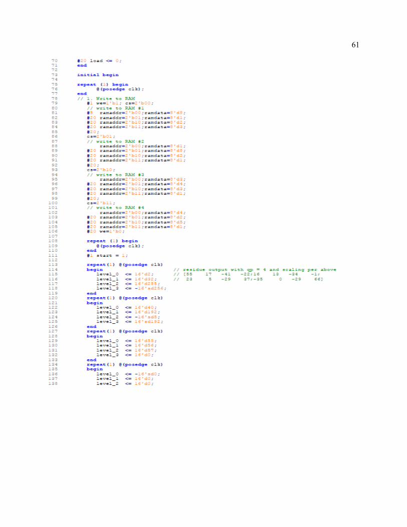
residueArray. The top level Verilog test bench is included in Appendix B and the MATLAB
files are included in Appendix C.
4.3 Synthesis
Synthesis is the process by which the RTL (Register Transfer Level) design is translated
into a gate-level netlist that targets a specific technology. For this work, the RTL design is done
in Verilog and the synthesis tool is Synopsys Design Compiler. The targeted technology is the
CMOS 45nm NANGATE FreePDK45 Library.

24
Results
The compilation of the Verilog modules to a gate-level netlist was aided by the use of the
make utility and a Tcl script file. The use of a make file and Tcl script ensure repeatability of the
compilation steps while also serving to capture the compiler/tool settings. The target clock
frequency of 200 MHz (5 ns) was chosen to provide adequate margin to meet the processing
needs of 4K UHD (3840 x 2160) at 30 frames/sec. For the ubiquitous 4:2:0 video format, the
total pixel rate for chroma and luma is 3840 x 2160 x 30 x 1.5 = 373,284,000 pixels/sec. This
design processes 2 pixels per clock, thus 200 MHz x 2 > 373,284,000 thus providing margin for
real time 4K video. The output files provided by the synthesis step are the gate level netlist,
top.vg, and the top.sdc file, which contains timing related information. Both of these files are
inputs to the place & route tool. The synthesis tool is also used to generate numerous reports
concerning power, timing, area, cell usage, etc. It is important to note that the reports produced
at the synthesis step are preliminary only, and do not take into account interconnect wiring.
However, it is still useful to review this information and verify if the design can meet
preliminary constraints or design goals. The following figures are used to show a key portion of
a particular report, highlighting the most relevant information. In Figure 14 a pertinent section
from the area report is shown.
Figure 14. Area, synthesis results
25
From this report, we see that the complete design uses a cell area of 13968 um2. From
this we can calculate the gate count in terms of the NAND2_X1 gate. The gate count, in terms
of a 2-input nand gate is used when comparing the size of one design to another independent of
the technology. The NAND gate of the Nan45 library has an area of 0.798 um2. Therefore, gate
count is totArea / nandArea = 17.5k gates. From an inspection of the timing report it is noted
that the setup slack of the critical paths is a worst case of 2.3 ns. This positive slack shows that
the design is capable of running at much higher frequencies, approximately 367 MHz. Lastly,
the pertinent section from the power report is shown in Figure 15.
The Tcl file used for synthesis generation is included in Appendix D.
4.4 Place and Route
The Nangate 45nm Open Cell Library was developed to provide a library for research,
testing, and exploring EDA flows. The Library contents include cell layouts, timing and power
libraries, geometric libraries, and a databook for all the library cells. The Nangate 45nm process
is a 10-metal layer with higher layers used for power and lower layers for signal routing. The
input files provided during physical design are the gate-level netlist file and the design
constraints file that passes timing information. In addition, an IO pin file is also provided to
place the pins in a logical and evenly distributed fashion. The place and route process is actually
Figure 15. Power, synthesis results

26
made up of a number of steps, and the granularity of these steps is dependent on the complexity
of the design. For this work, the following basic steps and their key issues are shown below.
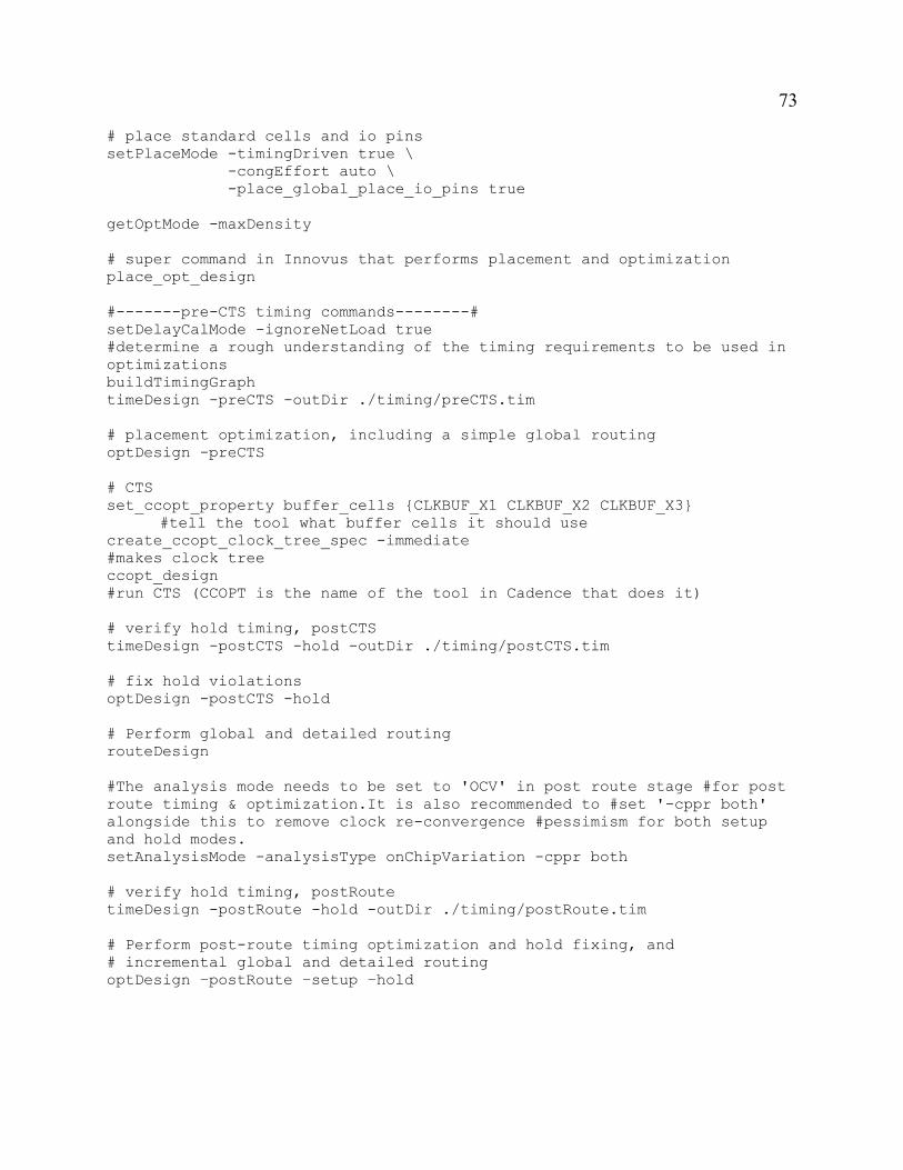
Floor Planning: Aspect Ratio, Core Utilization, I/O file, I/O to core clearances, double
back
Power Planning: Ring design, stripe design, local power rails
Placement: pre-placement and optimization of standard cells, post-placement and
optimization
Clock Tree Synthesis: Buffer selection, clock tree specification, clock tree routing
Routing: Global and detailed routing of all nets using timing and congestion driven
modes, post-route optimization.
Design Verification: DRC, Geometry, Connectivity
Floor Planning:
The floor planning step defines the size and shape of the die or core area. The shape is
typically a rectangle but can also take on recti-linear shapes if advantageous. The aspect ratio,
which is the ratio of die width / die height controls the shape and a value of ‘1’ indicates a square
rectangle. In addition, the core utilization is stipulated during this step and directly affects the
size of the core area. The utilization factor defines the percentage of area that will be used for
standard cell placement. For example, a value of 0.70 indicates that 70% of the die area will be
used for standard cell placement and the remaining 30% will be reserved and used as needed for
post-placement optimization. Most designs will begin with a utilization value of 0.70 and only
after successfully placed and routed, progressively increase this value to minimize core area. At
some point, as utilization increases, the design will take longer and longer to optimize as the area
for inserting optimization cells such as buffers will be limited.
Most designs allow for the placement of the cells in a row-by-row fashion. This,
however, places a limit on how closely the rows may be placed, due to the shorting that can
27
occur between the VDD pins of one row and the VSS pins of the abutting row. In order to avoid
this issue, double-back row placement is utilized in most designs. This simply means that every
other row is flipped so that the VSS of one row is adjacent to the next row. This not only allows
for tighter placement of rows but also results in more efficient routing of the local power rails
since the cell pins of adjacent rows can now be shorted together. The parameters used for the
floorplan in this work are summarized in Table 2.
Table 2. Floorplan Parameters
Parameter Value
Utilization 0.95
Aspect Ratio 1
Double Back True
Flip 1st Row True
IO to Core Space 20 um
The utilization factor was initially started at 0.70 and progressively increased until a final
value of 0.95 was achieved. A higher utilization value resulted in violations with parallel runs of
metal to metal within the IO to core spacing area. This spacing area has wide power rings which
introduce specific metal rules that must be adhered to.
Power Planning
In order to provide the necessary power required by a core area, a structure called a
power ring is utilized. The power ring is placed in the higher layer metals around the periphery
of the core area. The higher layer metals are thicker and also wider than the lower level metal
layers, and thus provide better conduction paths. The power ring is then supplemented with
straps or stripes that run in a vertical direction. In addition to the stripes, rails may also be
utilized. Finally, local power is carried to the standard cells by horizontal rails which connect to
28
the power and ground pins of the cells and then extend out to the power rings. The current that
the power rings carry can be roughly estimated by using the max power and then dividing by the
cell voltage and then by four, since each segment of the ring will carry approximately one-fourth
of the total power. The post-route analysis showed a power usage of 1.776 mW, which
corresponds to a current of 0.467 mA. Using this figure for current, one can determine a value
for current density based on the cross-sectional area of the power ring wires. For a wire width of
5 um and a thickness of 2 um on layers 9 and 10, this gives a current density of approximately
46.7 A/mm2. In an actual fabrication process, this figure should be compared to the foundry’s
guidance on maximum current density in a metal layer. The power mesh that results from the
placement of the power ring, stripes, and rails, makes up the power distribution network. The
picture in Figure 16 shows the network created during this design. The inner power ring is tied
to VDD while the outer power ring is tied to VSS. The power rings use metal layers 9 and 10,
with layer 10 providing the vertical segments and layer 9 horizontal segments. The vertical
stripes shown in light blue are placed on layer 8 and come in a pair, with one-half of each pair
supporting VDD or VSS. Finally, the horizontal rails shown in dark blue are at the lowest level,
metal 1, since the cell power pins are in metal 1.
29
Figure 16. Power network
30
Placement
The initial placement of the standard cells is done early in the design to asses timing and
congestion issues. This first step will use the constraints set forth during floor planning to guide
the placement of the cells listed in the gate-level netlist. Additionally, the IO pin file guides the
placement of cells so as to place cells close to their respective input or output pin. The
placement process has numerous switches that can be turned on or off as best determined by the
designer. For this design, timing driven placement was turned on and congestion effort was set
to ‘Auto’ which adjusts the effort level based on local areas of congestion. After this initial
placement and throughout the design process, timing information is generated using the
‘timeDesign’ command. This command will generate a series of reports that can be viewed to
find setup and hold violations as wells as design rule violations. The command is used with
switches to indicate either a pre or post phase of the design. The initial placement will also
generate global routing that is not fixed at this point but serves as a first pass routing of all the
nets. Following this step, optimization is performed and again after the clock tree is built and
then again after detail routing. The optimization command is ‘optDesign’ and it may be utilized
to correct design rule violations, correct hold time violations, optimize setup time, and
additionally the command utilizes certain techniques such as buffer insertion and area re-
claiming based on the design stage and options switched on or off. The following picture in
Figure 17 shows the cell placement of the finalized design.
31
Figure 17. Cell placement with 0.95 core utilization
As can be seen, the core area is highly utilized without any noticeable sparse areas. This view
shows the cell layout with a core utilization of 0.95.

32
In Figure 18 a zoomed in view of the cell placement with names of cell instances is
shown. It can be seen that the cells are closely packed together and abutted to each other in most
cases.
Figure 18. Zoomed in view of section of cell placement
Clock Tree Synthesis
Once the initial placement and optimization is performed, the clock tree synthesis (CTS)
step can begin. The purpose of the clock tree synthesis step is to provide a clock network that
reaches every flip-flop with minimal skew and latency. Latency or insertion delay is the delay
from the clock source to the sinks, and skew is the delay between the nearest sink and farthest
sink, in terms of time. Obviously, controlling the skew of the clock tree is critical to meeting
setup and hold time requirements. In addition to minimizing skew and latency, the clock tree
must also take into account such things as maximum allowed fanout, load capacitance, and
transition times. In order to meet these design requirements, the CTS process may use
techniques such as buffer insertion, upsizing driver cells, moving cells, and the use of wider
wires. One other key step in the CTS process is the identification of the buffers to be used in the
33
creation of the clock tree. The choice to use clock buffers as opposed to regular buffers is
recommended since they provide for balanced rise and fall times. This design specified that only
the NAN45 clock buffers be used for the clock tree. The picture in Figure 19 shows the
complete clock tree. The clock tree has numerous clock buffers that are used to balance the tree
and provide the drive strength to support the numerous sinks served by the branches.
Figure 19. Clock tree
34
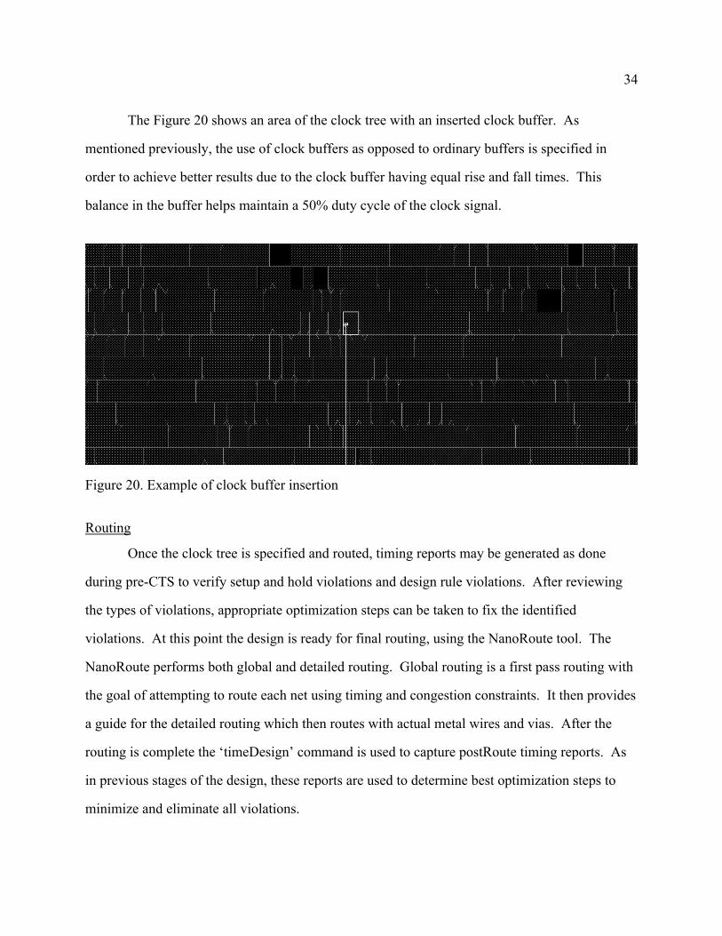
The Figure 20 shows an area of the clock tree with an inserted clock buffer. As
mentioned previously, the use of clock buffers as opposed to ordinary buffers is specified in
order to achieve better results due to the clock buffer having equal rise and fall times. This
balance in the buffer helps maintain a 50% duty cycle of the clock signal.
Figure 20. Example of clock buffer insertion
Routing
Once the clock tree is specified and routed, timing reports may be generated as done
during pre-CTS to verify setup and hold violations and design rule violations. After reviewing
the types of violations, appropriate optimization steps can be taken to fix the identified
violations. At this point the design is ready for final routing, using the NanoRoute tool. The
NanoRoute performs both global and detailed routing. Global routing is a first pass routing with
the goal of attempting to route each net using timing and congestion constraints. It then provides
a guide for the detailed routing which then routes with actual metal wires and vias. After the
routing is complete the ‘timeDesign’ command is used to capture postRoute timing reports. As
in previous stages of the design, these reports are used to determine best optimization steps to
minimize and eliminate all violations.

35
In Figure 21 a timing map showing the distribution of setup margin is shown, with red
showing areas with less margin and blue showing more margin.
Figure 21. Map of setup margin
To go along with the setup map, Figure 22 shows a map of hold margin for the design.
These maps can be used to find areas with timing concerns that can be addressed. For example,

36
if the timing map shows setup issues in a localized region, this may be an opportunity to
introduce additional pipelining.
Figure 22. Map of hold margin

37
In Figure 23 we see the complete design with all layers turned on and IO grouped
logically together.
Figure 23. Complete design

38
Design Verification
Once the design is fully routed and all timing violations have been eliminated, the next
step is to perform verification steps on the design. These verification steps ensure that the design
does not have any errors in the placement or routing. These errors, if left unchecked, may delay
the fabrication of the chip and in the worst case, render the design unusable. All three
verification tests passed with zero violations. The tests and a brief description of their scope is
provided below:
DRC: This verification step checks for basic checks such as required widths of shapes on
a layer, spacing between objects on a layer, and enclosure requirements of a feature such
as a via.
Geometry: Verifies internal geometries of wires and objects.
Connectivity: Checks for antennas, opens, loops and unconnected pins.
The Tcl commands used during the place and route are included in Appendix E.
Summary reports of the DRC, Geometry, and Connectivity verification reports are included in
Appendix F. As mentioned earlier, setup slack or margin was more than 2 ns from initial
placement and it was the hold margin that the optimization efforts were focused on to meet
timing. In Appendix G the post-route hold timing report summary is included.
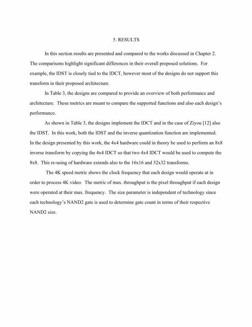
5. RESULTS
In this section results are presented and compared to the works discussed in Chapter 2.
The comparisons highlight significant differences in their overall proposed solutions. For
example, the IDST is closely tied to the IDCT, however most of the designs do not support this
transform in their proposed architecture.
In Table 3, the designs are compared to provide an overview of both performance and
architecture. These metrics are meant to compare the supported functions and also each design’s
performance.
As shown in Table 3, the designs implement the IDCT and in the case of Ziyou [12] also
the IDST. In this work, both the IDST and the inverse quantization function are implemented.
In the design presented by this work, the 4x4 hardware could in theory be used to perform an 8x8
inverse transform by copying the 4x4 IDCT so that two 4x4 IDCT would be used to compute the
8x8. This re-using of hardware extends also to the 16x16 and 32x32 transforms.
The 4K speed metric shows the clock frequency that each design would operate at in
order to process 4K video. The metric of max. throughput is the pixel throughput if each design
were operated at their max. frequency. The size parameter is independent of technology since
each technology’s NAND2 gate is used to determine gate count in terms of their respective
NAND2 size.
40
Table 3. Architecture and Performance Comparison
Design Tech. IDCT IDST Inverse Quant.
Size (gate count)
Max. Speed (MHz)
4K Speed (MHz)
Max Throughput (pixels/s)
[9] 130nm 8x8 no no 8.2ka comb. na unkown
[10] FPGA 28nm
4x4 no no na 78.31 23.3 835M
[12] 65nm 4x4-32x32 yes no 145.4k 500 412 410M
this work 45nm 4x4 yes yes 17.5k 367b 200 690M a NAND2 gate area of 5.0922 um2 b Based on setup margin

41
The design of Ma [9] is purely combinational logic and thus has no clock. The gate count
of Ma only includes one 1D transform and does not include the transpose memory. If we
estimate expected memory size using the design of this work, a register based 8x8 memory
would require approximately 9.5k gates and would bump the total gate count to roughly 25k
gates for a serially processed design, i.e. the transpose memory in between two IDCT modules.
In this work, the design re-uses the 1D transform to perform the 2D transform and thus achieves
some area savings.
The design of Porto [10] operates at a very high throughput due to the discarding of
columns of data and only performing one 1D inverse transform. It is unclear how effective this
technique would be when paired with lower QP values as the proposed design only discusses
high QP values. As mentioned previously, it also difficult to assess human perceived quality
from objective metrics. It is also unclear how effective the discarding of columns of data would
be with larger transform sizes.
The proposal of Ziyou [12] does implement the full range of transform sizes but does so
at a hefty gate count. Also, the design processes one coefficient at a time and so relies on a
higher clock speed than the other designs. This high clock speed would likely come with higher
power dissipation and possible emc issues.
6. CONCLUSION
In this work an HEVC compliant inverse quantization and transform has been presented
capable of processing 4K video at 30 frames/s. The design was entered in Verilog HDL,
synthesized, and then placed and routed in 45nm technology using industry standard tools. The
main components of video compression were discussed to give the reader a brief introduction to
how compression is achieved. The proposed design was then discussed at the various stages,
beginning with the RTL design and then proceeding to the synthesis and finally the place &
route. As the previous chapter demonstrated, the proposed design compares well with other
related works. It is the hope that the work undertaken herein will serve as a starting point for
other video compression projects. The HEVC standard will slowly but surely supplant the older
AVC standard. Newer standards will emerge and present new challenges that will need to be
solved in order to make them usable by video recording and imaging devices. Hopefully other
students at CSU, Fresno will find the subject of video compression interesting and will look for
opportunities within this technology to do their project and thesis work.
Moving forward, the support for larger transform sizes is one very obvious future work
that could be undertaken. Support for 8x8, 16x16, and 32x32 can be added to the existing
design. This would involve copying the 4x4 design and including an addition/subtraction
module to create an 8x8 transform circuit. Doing the same to this 8x8 circuit would then
produce a 16x16 transform circuit. This could again be applied to produce a 32x32 transform
circuit. This is a simplified view, but in principal is accurate. Another source for future
development is the transpose memory. Presently it is sized to support the 4x4 transform, this
would need to be increased in size to support 32x32. Specifically, the memory would need to be
32x32x16 bits in size. With this larger size, it would likely be beneficial, from an area
perspective, to design the memory to target SRAM memory instead of the simpler register based
design that was employed by this work.
43
It would be interesting to explore some throughput and power saving measures.
Specifically, zero-column skipping and data gating would be worth investigating and
implementing. The idea behind zero-column skipping is that for larger values of QP and in
particular for larger transforms, there is a higher probability of columns with all zero
coefficients, and thus identifying these columns and not performing the inverse transform on
these columns would increase throughput. As the design is extended to handle larger transform
sizes, the IDCT engine will process a mix of transform sizes and when the engine is handling
smaller transforms the unused circuitry will benefit from data-gating by preventing these paths
from toggling. Zero-column skipping and data gating have been reported in to increase
throughput by a minimum of 27% and reduce power by 18% [8].

REFERENCES
REFERENCES
[1] J. Ohm, W. Han, T. Wiegand and G. J. Sullivan, "Overview of the High Efficiency Video Coding (HEVC) Standard," IEEE Transactions on Circuits and Systems for Video Technology, vol. 22, no. 12, pp. 1649-1668, 2012.
[2] ITU-T and ISO/IEC, "ITU-T Rec. H.264 and ISO/IEC 14496-10 : Advanced Video Coding for Generic Audio-Visual Services," ITU-T and ISO/IEC, 2003.
[3] T. Wiegand, G. Sullivan, G. Bjontegaard and A. Luthra, "Overview of the H.264/AVC Video Coding Standard," IEEE Transactions on Circuits and Systems for Video Technology, vol. 13, no. 7, pp. 560-576, 2003.
[4] ITU-T and ISO/IEC, "ITU-T Rec. H.265 and ISO/IEC 23008-2: High Efficiency Video Coding," ITU-T and ISO/IEC, 2013.
[5] B. Juurlink, M. Alvarez-Mesa and C. Chi, "Understanding the Application: An Overview of the H.264 Standard," in Scalable Parrallel Programming Applied to H.264/AVC Decoding, Springer, 2012, pp. 5-15.
[6] G. Pastuszak and A. Abramowski, "Algorithm and Architecture Design of the H.265/HEVC Intra Encoder," IEEE Transactions on Circuits and Systems for Video Technology, vol. 26, no. 1, pp. 210-222, 2016.
[7] R. Bahirat and A. Kolhe, "Video Compression using H.264 AVC Standard," Intl Journal Emerg Rsrch Mngmnt & Tech, vol. 3, no. 2, pp. 31-37, 2014.
[8] V. Sze, M. Budagavi and G. J. Sullivan, High Efficiency Video Coding (HEVC): Algorithms and Architectures, London: Springer, 2014.
[9] T. Ma, C. Liu, Y. Fan and X. Zeng, "A Fast 8×8 IDCT Algorithm for HEVC," in 2013 IEEE 10th International Conference on ASIC, Shenzhen, 2013.
[10] M. Porto et al, "Hardware Design of Fast HEVC 2-D IDCT Targeting Real-Time UHD 4K Applications," in 2015 IEEE 6th Latin American Symposium on Circuits & Systems (LASCAS), Montevideo, 2015.
[11] H. B. A. Sheikh, "Image Information and Visual Quality," IEEE Transactions on Image Processing, vol. 15, no. 2, pp. 430-444, 2006.
[12] Y. Ziyou et al, "Area and Throughput Efficient IDCT/IDST Architecture for HEVC Standard," in 2014 IEEE International Symposium on Circuits and Systems, Melbourne, 2014.

46
[13] G. Tumbush, "Tumbush Enterprises," 14 February 2005. [Online]. Available: www.tombush.com. [Accessed 22 January 2019].
[14] M. El-Hadedy, S. Purohit, M. Margala and S. Knapskog, "Performance and Area Efficient Transpose Memory Arch. for High Throughput Adaptive Signal Proc. Systs.," in 2010 NASA/ESA Conf. on Adaptive Hardware and Systems, Anaheim, 2010.
[15] M. Tikekar, C. Huang, V. Sze and A. Chandrakasan, "Energy and Area-Efficient Hardware Implementation of HEVC Inverse Transform and Dequantization," in 2014 IEEE ICIP, Paris, 2014.
[16] S. Hsia and S. Wang, "Shift-Register-Based Data Transposition for Cost-Effective Discrete Cosine-Transform," IEEE Trans. on VLSI Systems, vol. 15, no. 6, pp. 725-728, 2015.
[17] L. Kerofsky and S. Riabtsev, "Dynamic Range Analysis of HEVC/H.265 Inverse Transform Operations," JCT-VC, Geneva, 2013.
[18] M. Braly, A. Stillmaker and B. Baas, "A Configurable H.265-compatible Motion Estimation Accelerator Architecture for Realtime 4K Video Encoding in 65 nm CMOS," in 2017 IEEE Conference on Dependable and Secure Computing, Taipei, 2017.
[19] M. Budagavi et al, "Core Transform Design in the HEVC Standard," IEEE Journal of Selected Topics in Signal Processing, vol. 7, no. 6, pp. 1029-1041, 2013.
[20] U. V. Group, "Kvazaar HEVC Encoder," 28 1 2014. [Online]. Available: ultravideo.cs.tut.fi. [Accessed 2 3 2019].
[21] I. Richardson, "An Overview of H.264 Advanced Video Coding," vcodex, 2019. [Online]. Available: www.vcodex.com/an-overview-of-h264-advanced-video-coding/. [Accessed 14 March 2019].

APPENDICES

APPENDIX A: VERILOG FILES
49

50
51

52

53
54
55

56

57
58

APPENDIX B: VERILOG TESTBENCH

60
61
62

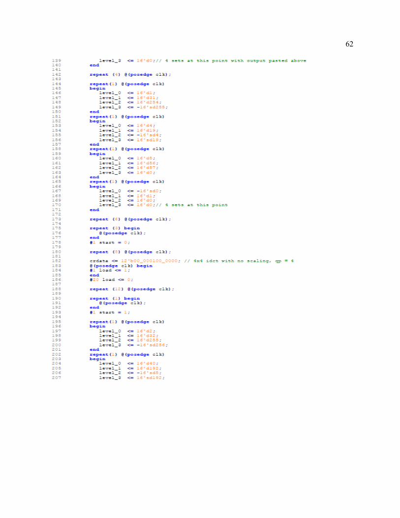
63

APPENDIX C: MATLAB FILES

65
function [ residueArray ] = rcArrayFunction(qp, levelArray, freqArray) % rcArrayFunction This function accepts an array of level values and % a scaling array of any size and the scalar value called qp. % On each element of the input array, the "main_Dequantization" % function is performed and the results are stored in an output array % of the same size as the input array. Finally we inverse transform and return % results in residueArray. [rows, cols] = size(levelArray); outputArray = int32(zeros(rows,cols)); % makes an array of zeros to store result tempArray = int32(levelArray .* freqArray); % performs freq. scaling of input array disp(tempArray); % these nested for-loops take each element in the input array one value at % a time and pass it through the "main_Dequantize" function. The reslt is % stored in "outputArray." for ix = 1:rows for jx = 1:cols outputArray(ix,jx) = main_Dequantize(qp, tempArray(ix,jx)); end end % the outputArray stores the dequantized values. Next we call function % that performs inverse transform and store result in residueArray residueArray = my4x4Function(double(outputArray)); end

66
function [coeff] = main_Dequantize(qp, level) qp = int8(qp); level = int32(level); offsetIQ = int32(16); shift1 = int32(-5); switch mod(qp,int8(6)) case 0 gmod = int8(40); case 1 gmod = int8(45); case 2 gmod = int8(51); case 3 gmod = int8(57); case 4 gmod = int8(64); case 5 gmod = int8(72); otherwise gmod = int8(40); end gmod = int16(gmod); exp = idivide(qp,6); step = int32(bitshift(gmod,exp)); %coeff = step; temp = (level*step + offsetIQ); %disp(temp); coeff = bitshift(temp, shift1); end

67
function [resArray] = my4x4Function(coeffArray) d1 = [64,64,64,64]; d2 = [83,36,-36,-83]; d3 = [64,-64,-64,64]; d4 = [36,-83,83,-36]; %--------- Matrix Declaration ---------% % 4x4 DCT matrix DCT4 = [d1;d2;d3;d4]; %Bit Depth B B = 8; %Matrix Size M4 = 4; %---------- Offset Factors -----------% %Inverse Stage Offset %OIT1 = SIT1/2; %OIT2 = SIT2/2; %---------- Scaling Factors -----------% %Inverse Stage Scaling SIT1 = 2^7; SIT2 = 2^(20-B); %Forward Stage Scaling ST4 = 2^-(B+log2(M4)-9); ST42 = 2^-8; %--------- Input Declaration ---------% %random input % 4 point input %in4 = randi(256,4); in4 = coeffArray; %--------------- OUTPUT ---------------% %---------------- 4 X 4 1st Stage ---------------% inv4_s1 = (transpose(DCT4)*in4) / SIT1; % uses 1st array rnd1 = floor(inv4_s1); % rounding down 1st array %---------------- 4 X 4 2nd Stage ---------------% inv4 = ((inv4_s1*DCT4)) / SIT2; % unrounded array #1, standard DCT equation rnd2 = (transpose(DCT4)*transpose(rnd1)) / SIT2; % rounded array #1, Verilog math resArray = floor(rnd2); % final rounding array #1

APPENDIX D: SYNTHESIS TCL FILE
69
# dc-top.tcl script # # 2018/02/15 Added *_ANALYZE_SECTION comments to new Makefile can automatically # add .v files to dc-*.tcl. Also updated some comments. # 2017/02/14 Reduced output_delay to 4% and input_delay to 3% of the clock # cycle time so very short critical paths are visible in timing # reports. Also changed clock_skew from 250ps to 5% of cycle time # so it will scale with clock frequency. # 2017/02/10 Uncommented "analyze -format verilog ./proc.v" line. It seems to # be needed only the first time synthesis is run. # 2017/02/04 Changes for NanGate 45 nm library including new timing parameters # 2012/02/22 Changed: # ungroup -all -flatten -simple_names # to: # if { [sizeof_collection [get_cells * -filter # "is_hierarchical==true"]] > 0 } { # ungroup -all -flatten -simple_names # } # 2010/02/16 Updated commented path to vtvtlib25.db # 2009/02/12 Many parts re-written in new tcl version by Zhibin Xiao # 2006/01/30 Updated /afs/.../vtvtlib25.db path to this quarter's path. # 2004/02/05 Updated /afs/.../vtvtlib25.db path to this quarter's path. # 2003/05/22 Increased input_setup from 500 to 6000 (external input delay # now 6ns instead of 9.5ns) so input paths don't show up at the # top of timing reports so often. # 2003/05/15 Cleaned up a little # 2003/05/14 Written # # Debugging # list -designs # list -libraries # list -files # # Add if you like: # Annotates inputs, but doesn't propagate through design to clear warnings. # set_switching_activity -toggle_rate 0.25 -clock "clk" { "in31a" } # More power info # report_power -net # report_power -hier # set_max_delay # write -format db -output top.db # # Doesn't work quite the way I expect # NameDesign = top Set variable ok, but how to concatenate? # write_rtl -format verilog -output top.vg

70
#===== Set: make sure you change design name elsewhere in this file set NameDesign "top" #===== Set some timing parameters set CLK "clk" #===== All values are in units of ns for NanGate 45 nm library set clk_period 5 #set clock_skew [expr {$clk_period} * 0.05 ] set clock_skew 0.050 set input_setup [expr {$clk_period} * 0.97 ] set output_delay [expr {$clk_period} * 0.04 ] set input_delay [expr {$clk_period} - {$input_setup}] # It appears one "analyze" command is needed for each .v file. This works best # (only?) with one command line per module. analyze -format verilog top.v analyze -format verilog control.v analyze -format verilog transpose_4x4.v analyze -format verilog shift_reg.v analyze -format verilog idct.v analyze -format verilog dequantizer.v analyze -format verilog single_port_ram.v elaborate $NameDesign current_design $NameDesign link uniquify if { [sizeof_collection [get_cells * -filter "is_hierarchical==true"]] > 0 } { ungroup -all -flatten -simple_names } set_max_area 0.0 #===== Timing and input/output load constraints create_clock $CLK -name $CLK -period $clk_period -waveform [list 0.0 [expr {$clk_period} / 2.0 ] ] set_clock_uncertainty $clock_skew $CLK #set_clock_skew -plus_uncertainty $clock_skew $CLK #set_clock_skew -minus_uncertainty $clock_skew $CLK set_input_delay $input_delay -clock $CLK [all_inputs] #remove_input_delay -clock $CLK [all_inputs] set_output_delay $output_delay -clock $CLK [all_outputs] #disable reset from timing constraints, incorrectly flagged by tools set_false_path -from rstn
71
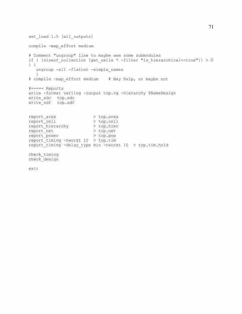
set_load 1.5 [all_outputs] compile -map_effort medium # Comment "ungroup" line to maybe see some submodules if { [sizeof_collection [get_cells * -filter "is_hierarchical==true"]] > 0 } { ungroup -all -flatten -simple_names } # compile -map_effort medium # May help, or maybe not #===== Reports write -format verilog -output top.vg -hierarchy $NameDesign write_sdc top.sdc write_sdf top.sdf report_area > top.area report_cell > top.cell report_hierarchy > top.hier report_net > top.net report_power > top.pow report_timing -nworst 10 > top.tim report_timing -delay_type min -nworst 10 > top.tim.hold check_timing check_design exit

APPENDIX E: PLACE & ROUTE COMMANDS
73
# place standard cells and io pins setPlaceMode -timingDriven true \ -congEffort auto \ -place_global_place_io_pins true getOptMode -maxDensity # super command in Innovus that performs placement and optimization place_opt_design #-------pre-CTS timing commands--------# setDelayCalMode -ignoreNetLoad true #determine a rough understanding of the timing requirements to be used in optimizations buildTimingGraph timeDesign -preCTS -outDir ./timing/preCTS.tim # placement optimization, including a simple global routing optDesign -preCTS # CTS set_ccopt_property buffer_cells {CLKBUF_X1 CLKBUF_X2 CLKBUF_X3} #tell the tool what buffer cells it should use create_ccopt_clock_tree_spec -immediate #makes clock tree ccopt_design #run CTS (CCOPT is the name of the tool in Cadence that does it) # verify hold timing, postCTS timeDesign -postCTS -hold -outDir ./timing/postCTS.tim # fix hold violations optDesign -postCTS -hold # Perform global and detailed routing routeDesign #The analysis mode needs to be set to 'OCV' in post route stage #for post route timing & optimization.It is also recommended to #set '-cppr both' alongside this to remove clock re-convergence #pessimism for both setup and hold modes. setAnalysisMode -analysisType onChipVariation -cppr both # verify hold timing, postRoute timeDesign -postRoute -hold -outDir ./timing/postRoute.tim # Perform post-route timing optimization and hold fixing, and # incremental global and detailed routing optDesign –postRoute –setup –hold

74
APPENDIX F: VERIFICATION REPORTS
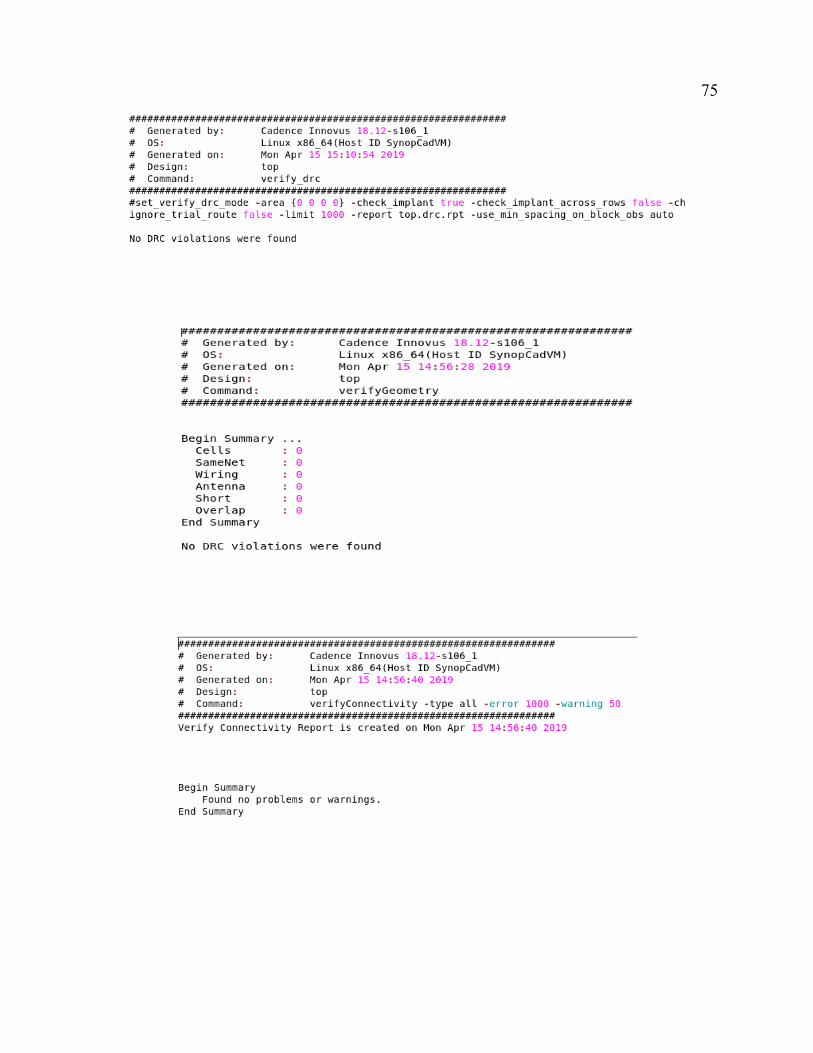
75

APPENDIX G: HOLD TIMING SUMMARY

77