Embed Size (px)
Citation preview
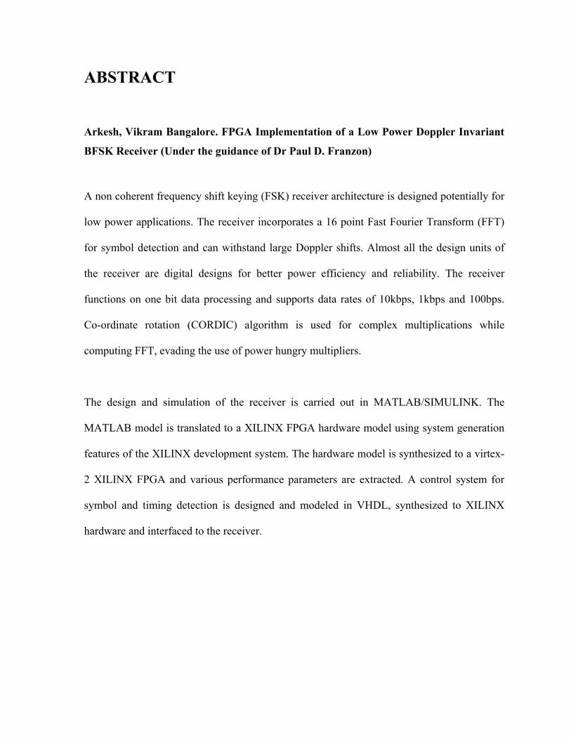
ABSTRACT
Arkesh, Vikram Bangalore. FPGA Implementation of a Low Power Doppler Invariant
BFSK Receiver (Under the guidance of Dr Paul D. Franzon)
A non coherent frequency shift keying (FSK) receiver architecture is designed potentially for
low power applications. The receiver incorporates a 16 point Fast Fourier Transform (FFT)
for symbol detection and can withstand large Doppler shifts. Almost all the design units of
the receiver are digital designs for better power efficiency and reliability. The receiver
functions on one bit data processing and supports data rates of 10kbps, 1kbps and 100bps.
Co-ordinate rotation (CORDIC) algorithm is used for complex multiplications while
computing FFT, evading the use of power hungry multipliers.
The design and simulation of the receiver is carried out in MATLAB/SIMULINK. The
MATLAB model is translated to a XILINX FPGA hardware model using system generation
features of the XILINX development system. The hardware model is synthesized to a virtex-
2 XILINX FPGA and various performance parameters are extracted. A control system for
symbol and timing detection is designed and modeled in VHDL, synthesized to XILINX
hardware and interfaced to the receiver.

FPGA IMPLEMETATION OF A LOW POWER DOPPLER INVARIANT BFSK RECEIVER
by Vikram B Arkesh
A thesis submitted to the Graduate Faculty of
North Carolina State University in partial fulfillment of the requirements for the degree in
Master of Science in Electrical Engineering
Department of Electrical and Computer Engineering
Raleigh 2003
Approved by:
________________________
Dr. Paul D. Franzon Chairman, Advisory Committee
_____________________ _____________________
Dr. Rhett Davis Dr. J Keith Townsend

ii
DEDICATION
To my parents, Arkesh and Sudha

iii
BIOGRAPHY
Vikram Arkesh was born in Secunderabad, India in January 1978. He graduated from
Bangalore University, Bangalore, India with a Bachelor’s degree in Electronics and
Communication in August 2000. He worked at Robert Bosch, Bangalore, India from
September 2000 to August 2001 as software engineer in the area of communication
applications. In the fall of 2001, he enrolled in North Carolina State University as a graduate
student to pursue M.S in Electrical Engineering. He worked on his MS thesis under the
guidance of Dr Paul Franzon from May 2002 to August 2003.

iv
ACKNOWLEDGEMENTS
First of all I would like to thank my thesis advisor, Dr Paul Franzon for having given me
such a wonderful opportunity. It was truly a very interesting and exciting experience to have
worked on my thesis topic. I would like to thank Dr Rhett Davis for all his support and
guidance on the XILINX tool set. I would like to thank Dr Keith Townsend for all his time
and support. This thesis work would have been impossible without the help and guidance of
my friends John Damiano, Mehmet Yuce, and Bhaskar Bharat; thank you very much.
Last but not the least, I would like to thank my parents, Arkesh and Sudha and my sister,
Chitra for being a constant source of inspiration and motivation for the entire tenure of my
Masters course.

v
TABLE OF CONTENTS
List of Figures vii
List of Tables viii
1 Introduction…………………………………………………………………………… 1 1.1 Organization of the thesis………………………………………………………. 2
2 FSK Systems, an Overview…………………………………………………………... 3
2.1 Frequency Shift Keying………………………………………………………… 3 2.2 Binary FSK System…………………………………………………………….. 4 2.3 FSK Detection………………………………………………………………….. 6
2.3.1 Coherent Binary FSK Detector…………………………………………. 7 2.3.2 Non Coherent Binary FSK Detector……………………………………. 8 2.3.3 Introduction to FFT based Detectors………………………………….... 9
2.4 Co-ordinate Rotation Algorithm (CORDIC)………………………………….... 10
3 FSK Receiver Architecture…………………………………………………………… 12 3.1 Motivation…………………………………………………………………….... 12 3.2 Overview of the Receiver Architecture………………………………………… 13 3.3 The need of Sub Sampling……………………………………………………… 15 3.4 Noise Effects due to 1-bit quantization……………………………………….... 17 3.5 Detection Mechanism………………………………………………………....... 18 3.6 Control System…………………………………………………………………. 21
4 SIMULINK Model……………………………………………………………………. 22
4.1 Introduction to SIMULINK…………………………………………………….. 22 4.2 SIMULINK Model of the Receiver…………………………………………….. 24 4.3 Simulations……………………………………………………………………... 26 4.4 Verification……………………………………………………………………... 33
4.4.1 Receiver Performance to Doppler Shifts……………………………….. 33 4.4.2 Receiver BER Performance…………………………………………….. 34 4.4.3 Receiver performance to variations in A/D clock……………………… 36
5 XILINX Implementation of the Receiver……………………………………………. 37
5.1 Introduction to System Generation in XILINX………………………………... 37 5.1.1 System Generation Design Flow………………………………………. 38
5.2 XILINX Model - Top level system……………………………………………. 39 5.3 XILINX Model - Down Conversion…………………………………………… 41 5.4 XILINX Model – FFT Detector……………………………………………….. 43 5.5 Synthesis to XILINX FPGA…………………………………………………… 47

vi
6 Conclusion and Future Work………………………………………………………… 48 6.1 Future Work……………………………………………………………………. 48
7 Bibliography………………………………………………………………………….. 49
8 Appendix……………………………………………………………………………… 50

vii
List of Figures 2.1 Binary FSK waveform…………………………………………………………….. 4
2.2 Signal Space of BFSK……………………………………………………………… 5
2.3 Coherent BFSK Receiver…………………………………………………………. 7
2.4 Quadrature Receiver for non coherent Detection………………………………. 8
3.1 FSK Receiver System Diagram ………………………………………………….. 13
3.2 Effect of Sub Sampling……………………………………………………………. 15
3.3 FFT Detector………………………………………………………………………. 19
3.4 Control System Block Diagram…………………………………………………... 20
4.1 SIMULINK Model of the FSK Receiver…………………………………………. 23
4.2 Transmitted waveform and Received Digitized Waveform…………………….. 26
4.3 Down Conversion Waveform……………………………………………………... 27
4.4 Decimated Waveform……………………………………………………………… 28
4.5 Input data matrix to the FFT Detector…………………………………………… 29
4.6 Output data matrix after FFT Computation…………………………………….. 30
4.7 Receiver output after symbol detection…………………………………………… 31
4.8 Output of the Bernoulli Transmitter……………………………………………… 31
4.9 FFT Detector output after Doppler shift of 5 KHz………………………………. 32
4.10 BER plot for the three data rates………………………………………………... 35
5.1 XILINX System Generation Design Flow………………………………………… 38
5.2 XILINX Model top level system diagram………………………………………… 39
5.3 Receiver Model Implemented in XILINX………………………………………… 40
5.4 XILINX hardware model of the down conversion operation………………….... 41
5.5 XILINX hardware model of the FFT Detector…………………………………... 43
5.6 Subsystem to implement the sum of real and imaginary parts for
FFT computation…………………………………………………………………… 44
5.7 Subsystem to implement a rotation of 45o for FFT computation……………….. 45
5.8 Subsystem to implement a rotation of 22.5o for FFT computation……………… 45
5.9 Waveforms displayed after symbol detection……………………………………. 46

viii
List of Tables
3.1 Receiver Specification………………………………………………………………. 13
4.1 Performance of the Receiver to Doppler Shifts…………………………………… 34
4.2 BER Performance of the Receiver…………………………………………………. 34
4.3 Receiver performance to clock variation at A/D converter………………………. 36

1
Chapter 1
Introduction
Wireless communication is one of the fastest growing fields owing to its length and breadth
of applications. Deep space communication is one such field where the use of wireless
systems is indispensable. The most important issue in space communication is power and
happens to be one of the major driving forces in the quest for low power wireless systems.
We focus on the design of a low power FSK receiver intended specifically for deep space
communications that involves an orbiter and a lander.
A typical set up in space explorations will involve an orbiter, orbiting a planet or a satellite
and a lander which is on the planet or satellite and which is in communication with the
orbiter. In such a scenario, there exists a relative displacement between the orbiter and
lander. This results in Doppler shifts in the transmitted/received signal and could potentially
introduce detection errors in the receiver. Hence, the receiver designed for such applications
should be invariant to Doppler changes in frequency.
A receiver architecture based on frequency shift keying is proposed by Grayver [1] which
uses an FFT detection scheme. The receiver can take care of Doppler shifts and has almost
all digital architecture intended for low power applications. We explore this architecture for
the FSK receiver design. The FFT computation in the receiver involves non trivial complex
multiplications suggesting the need to use power consuming multipliers. The FFT algorithm
proposed by Bertazonni [2] uses co-ordinate rotation algorithm (CORDIC) in place of
complex multiplications. CORDIC algorithm works on the principle of rotating the complex
phasors instead of multiplying them and uses adders/shifters. We explore a CORDIC
approach for FFT computation to improve power efficiency.

2
The receiver is designed and modeled in MATLAB and SIMULINK. We simulate the
receiver and test it for data rates of 10kbps, 1kbps and 100bps. We design an FSK transmitter
and introduce additive white Gaussian noise and Doppler shifts in the transmitted signal and
test the receiver for such conditions.
We port the SIMULINK model to a XILINX hardware model using the system generation
features and block sets of SIMULINK. The block set contains various building blocks for
digital signal processing, communication and math operations. We simulate the XILINX
model in SIMULINK and synthesize the model to a VIRTEX-2 FPGA using XILINX’s
optimized logiCOREs. Then we perform static timing analysis and power analysis of the
synthesized design. A control system is designed and developed in VHDL to take care of
symbol and timing detection of the receiver. The system is tested, synthesized to XILINX
hardware and interfaced to the receiver.
1.1 Organization of the thesis
Chapter 2 gives an introduction to FSK systems and the design entities used in the receiver.
Chapter 3 describes the FSK receiver design and control system design in detail. Chapter 4
describes the MATLAB model, the simulation results, waveforms and analysis. Chapter 5
describes the XILINX hardware model and synthesis results. Chapter 6 gives a summary of
the thesis and suggests future work that can be done in the direction of this thesis.

3
Chapter 2
FSK Systems, an Overview
Digital modulation is the process by which digital symbols are transformed into waveforms
that are compatible with the characteristics of the channel. In the case of baseband
modulation these waveforms are pulses, but in the case of band pass modulation, the desired
information signal is modulated to a sinusoid called a carrier wave. FSK modulation is a
class of band pass modulation in which the frequency of the carrier varies in accordance with
the information signal.
2.1 Frequency shift keying (FSK):
Frequency Shift Keying (FSK) system is a class of wireless systems that is very popular
today and has widespread applications. An FSK system carries its information in the
instantaneous frequency of the received signal. For e.g. a binary FSK system which transmits
the symbols 0 and 1 have one frequency corresponding to the symbol 0 and another
frequency to the symbol 1.
FSK systems are broadly classified into Coherent and Non-coherent systems. A coherent
system requires carrier or phase synchronization at the receiver end in order to detect the
signals whereas non coherent detection does not require any sort of synchronization.
Consequently the design of non coherent systems is much simpler when compared to
coherent systems making them more popular when power is an important concern. But non
coherent systems have a BER performance of 3db less than the traditional coherent receiver
at a BER of 10E-5.

4
The general analytic expression for FSK modulation is
( ) ( )φω += tTEts ii cos2
where si(t) is the modulated carrier, E is the energy content of si(t) over each information
symbol of duration T, ωi is the frequency term with M discrete values, and the phase term, ф
is an arbitrary constant. (ωi+1 - ωi) is typically assumed to be an integral multiple of Π/T
since FSK is implemented as orthogonal signaling where each tone in the signal set cannot
interfere with any other tones. In case of binary FSK, the value of M is two, representing
binary information symbols and a carrier with two possible frequencies.
2.2 BINARY FSK SYSTEM:
Fig 2.1: Binary FSK waveform
The binary FSK waveform displayed in Fig 2.1 illustrates the typical abrupt frequency
changes at the symbol transitions. The top waveform represents the information symbols and
the bottom waveform represents the modulated carrier signal. It can be seen that symbol ‘1’
0 ≤ t ≤ T i = 1,…., M
BIT 0 BIT 1
INFORMATION WAVE
BFSK WAVE
5
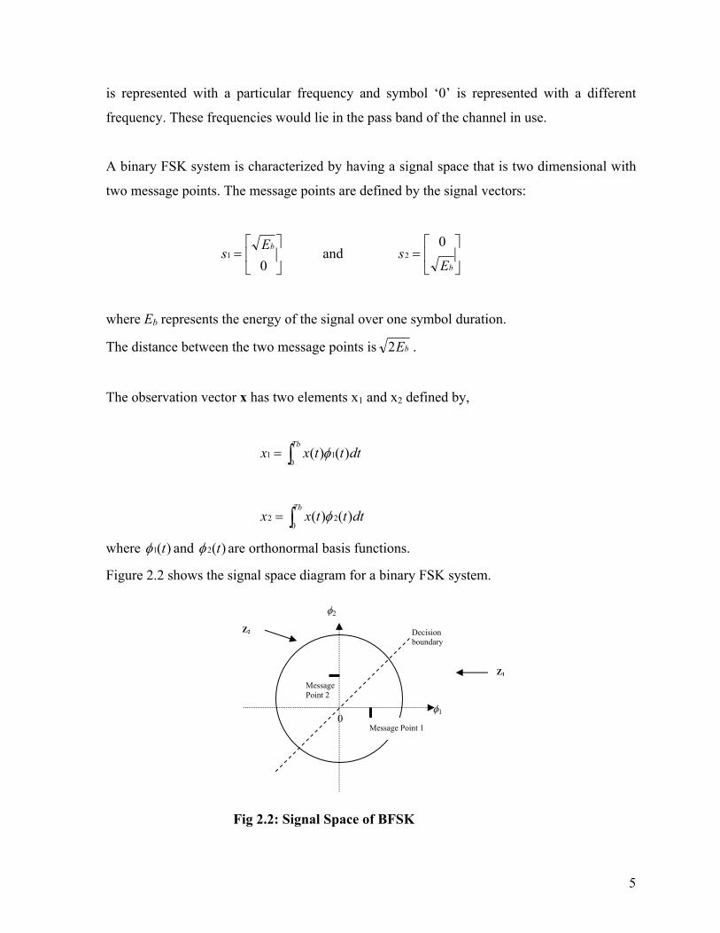
φ2
is represented with a particular frequency and symbol ‘0’ is represented with a different
frequency. These frequencies would lie in the pass band of the channel in use.
A binary FSK system is characterized by having a signal space that is two dimensional with
two message points. The message points are defined by the signal vectors:
=
01
bEs and
=
bEs
02
where Eb represents the energy of the signal over one symbol duration.
The distance between the two message points is bE2 .
The observation vector x has two elements x1 and x2 defined by,
∫=Tb
dtttxx0
11 )()( φ
∫=Tb
dtttxx0
22 )()( φ
where )(1 tφ and )(2 tφ are orthonormal basis functions.
Figure 2.2 shows the signal space diagram for a binary FSK system.
Fig 2.2: Signal Space of BFSK
Message Point 2
0φ1
Decision boundary
Message Point 1
Z1
Z2

6
The observation space is partitioned into two decision regions, labeled as Z1 and Z2.
Accordingly the receiver decides in favor of symbol 1 if the received signal point represented
by the observation vector x falls inside region Z1 i.e. when x1>x2 else the receiver decides in
favor of symbol 0.
2.3 FSK DETECTION:
FSK detection is the process of extracting the information symbols from a modulated carrier
wave. The detection process is mainly categorized into two types namely; coherent detection
and non coherent detection. In the case of coherent detection, the receiver exploits the
knowledge of the carrier’s phase in order to detect the symbols whereas in the case of non
coherent detection, the receiver does not utilize any phase reference information from the
carrier. Coherent based receivers are usually complex to design but have the best BER
performances. Also, coherent designs consume a lot of power. Non coherent receivers have
simple design, consume less power but have reduced BER performances.
In the context of the present receiver design for deep space exploration, the receiver power is
a very important issue and since the transmitter power can be elevated, power is traded for
reduced BER performance.

7
2.3.1 Coherent binary FSK detector:
Figure 2.3 shows the block diagram of a coherent binary FSK receiver which is used
commonly. As mentioned in the previous section a coherent receiver needs to be in phase
synchronization with the transmitter. It consists of two correlators with a common input and
which are supplied with two locally generated reference signals )(1 tφ and )(2 tφ . The
correlator outputs are then subtracted one from another and the resulting difference ‘d’ is
compared with a threshold of zero volts. If d>0, the receiver decides in favor of 1 else in
favor of 0. The transmitted signal consists of both the frequencies f1 and f2. The reference
signals )(1 tφ and )(2 tφ are extracted by applying the received signal to a pair of narrow band
filters, one tuned to f1 and the other tuned f2. Hence the reference signals are in phase
coherence with the transmitted signals.
Fig 2.3: Coherent BFSK receiver
INTEGRATORx
+ DECISION
INTEGRATORx
x(t)
Φ1(t)
Φ2(t)
+
_d
1 if d>00 if d<0

8
2.3.2 Non Coherent binary FSK detector:
Fig 2.4: Quadrature receiver for non coherent detection
Figure 2.4 depicts the block diagram of a non coherent binary FSK detector. Since phase
information of the carrier is absent, the detector is implemented as an energy detector. As we
can see, the receiver consists of two channels namely; the in phase (I) channel and the
quadrature phase (Q) channel. The two branches of the I channel are configured to detect the
signal with frequency w1; the reference signals being T/2 cos(w1t) for the ‘I’ branch and
T/2 sin(w1t) for the ‘Q’ branch. A similar arrangement exists for the detection of signal
with frequency w2 as can be seen from the two branches of the Q channel. The blocks
following the product integrators perform a squaring operation to prevent the appearance of
any negative values. A difference of the energies of the channels I and Q is calculated and
fed to the decision stage which decides in favor of w1 if the difference is greater than zero
else in favor of w2. The quadrature non coherent detector requires twice as many branches as
the coherent detector and is not very power efficient.
INTx SQU
INTx SQU
+
INTx SQU
INTx SQU
+
+ DECISION
fc1
fs1
fc2
fs2
x(t)
I CHANNEL
Q CHANNEL
I CHANNEL
Q CHANNEL
+
_
z

9
Another common implementation for non-coherent detection is the envelope detector where
band pass filters and envelope detectors are used. An envelope detector consists of a rectifier
and a low pass filter. The detectors are matched to the signal envelopes rather than the
signals themselves and a decision as to whether a one or a zero was transmitted is made on
the basis of which two envelope detectors have the largest amplitude. Although the envelope
detector has a simpler design as compared to the quadrature detector, the fact that quadrature
detectors can be implemented digitally as VLSI circuits and also the use of filters and
rectifiers in the envelope detectors increase their power requirement and cost than the
quadrature detector.
2.3.3 Introduction to FAST FOURIER TRANSFORM (FFT) based detectors
Speaking of energy detection in non-coherent FSK systems, the Discrete Fourier Transform
(DFT) based detection is another method which is gaining importance today. The DFT is a
powerful tool used to perform spectrum analysis of discrete time signals. The N point DFT of
a sequence x(n) of length N is given by the formula,
∑−
=
=1
0)()(
N
n
knNWnxkX 0 ≤ k ≤ N-1
The sequence X(k) can be thought of as a bank of N correlators, each representing the energy
of the signal for a particular frequency which is used for analysis and detection. The
advantage of using DFT for detection lies in its capability to handle Doppler shifts in the
received signal. But, DFT computation as it is requires N2 complex multiplications and N2–N
complex additions which make DFT impossible to implement especially for large values of
N.
Fast Fourier Transform (FFT) algorithms [3] are a set of computationally efficient algorithms
used to compute the DFT and have made the implementation of DFT a reality. These

10
algorithms work on the basis of a divide and conquer approach, by decomposing an N point
DFT into successively smaller DFT computations and finally aggregating the result. The FFT
algorithms bring about a phenomenal improvement in speed and computational efficiency of
the DFT. For e.g. the radix 2 FFT algorithm [3] which is one of the most widely used FFT
algorithms, requires a total number of (N/2)log2N complex multiplications and Nlog2N
complex additions. The speed improvement factor by using the radix 2 FFT algorithms for
sequences of size 1024 is about 200 and is better for larger sequences. The introduction of
CORDIC algorithms to perform complex multiplications in FFT has improved the power
efficiency of FFT computation to a very large extent and has made FFT based detection a
very attractive choice for low power FSK receivers.
2.6 CO-ORDINATE ROTATION ALGORITHM (CORDIC):
The CORDIC (Co-ordinate Rotation Digital Computing) algorithm is a time and space
efficient algorithm mainly used to calculate the Sine and Cosine of a given angle. The
algorithm replaces multiplication/division by shift operations resulting in time and space
efficiency. The only expensive operation in the computation is addition. The algorithm is
commonly used in sine and cosine generation, polar-Cartesian conversions, and vector
rotation.
An illustration of the CORDIC algorithm is given here. In FFT computations, a complex
number is multiplied by the factor iNW which corresponds to a phase rotation of 2пi / N. For
e.g. let A = x + jy and iNW = ej26.56
Therefore A ej26.56 = (x + jy)(cos(26.56) + jsin(26.56))
We could write the above product as,
A ej26.56 = X1 + jY1

11
Where
X1 = cos(26.56) ( x - ytan(26.56))
And
Y1 = cos(26.56) ( y + xtan(26.56))
But tan(26.56) ≈ 21
And cos(26.56) ≈ 21 + 22
1 + 321 + 62
1
As we can see, the “tan” and “cos” can be implemented as shift operations and the rest of the
computations are simple additions. Shifters and adders are relatively simple to implement
and have better space and time efficiency.

12
CHAPTER 3
FSK RECEIVER ARCHITECTURE
3.1 Motivation:
There are a lot of FSK detectors in the market today depending upon the application of
interest. As mentioned previously, coherent receivers are the best in terms of BER
performances but have complex system design and consume more power. Also, coherent
designs require fine frequency tracking making them very sensitive to Doppler shifts and
require a longer frequency acquisition time. The non coherent receivers currently used do not
meet the power requirement and Doppler shift requirement demanded by the application of
interest.
The objective of the receiver design is to have an all digital architecture. Digital designs are
preferred over their analog counterparts mainly for the following reasons:
a) CMOS digital circuits consume very less power than their analog counterparts. They
can have sleep modes that allow the system to be completely shut off when no
processing is done.
b) Digital designs have no portability issues when it comes to fabricating the design
using a better fabrication process that consumes lesser power and size.
c) Digital circuits are less sensitive to changes in temperature, pressure and aging.
As mentioned earlier, the receiver is targeted for communications between an orbiting ship
and a planetary landing vehicle. This scenario has important ramifications that motivate to
optimize the receiver architecture and they are:
a) The power consumption of the receiver of the planetary lander is more critical than
the transmission power of the orbiting vehicle.
b) There is no adjacent channel interference, hence the noise is additive white Gaussian.

13
Since power is an important concern at the receiver of the lander, the design trades off
transmit power against the receiver power. Since noise is only additive white Gaussian, the
design trades off BER performance to power consumption by implementing a non coherent
architecture.
3.2 Overview of the receiver architecture:
Fig 3.1: FSK receiver system diagram
Table 3.1: Receiver Specification
Modulation type Binary Frequency Shift Keying
Carrier Frequency 473.1 MHz
Data rates 100bps, 1kbps and 10kbps
Doppler Shift ± 10 KHz
AMPSAW
A/D X 24
10
10 MUX FFT SYMBOLDECISION
DATA
RECEIVEDSIGNAL
ej

14
Table 3.1 shows the receiver specifications and Fig 3.1 shows the proposed receiver
architecture. The received signal is amplified by a power efficient, low noise amplifier. The
amplified signal is filtered with a surface acoustic wave filter. The filtered signal is sub
sampled and digitized to 1-bit precision using a 1-bit A/D converter. The carrier frequency of
the received signal is 473.1 MHz and this signal is subsampled at 1.2 MHz. Sub sampling is
an excellent way to reduce power consumption since the circuit is made to operate at a much
lower frequency even though the received signal frequency is centered at a higher value. The
reason to choose a sampling frequency of 1.2MHz is dealt with in the succeeding sections.
The process of 1 bit A/D conversion also leads to a simple and power efficient detector
design. Moreover 1 bit quantization is a highly non linear operation which means that the
preceding analog components need not be linear and no AGC circuit is needed. Non-linear
amplifiers and samplers use considerably less power than their analog counter parts.
The one bit digitized signal is downconverted and decimated to baseband by first multiplying
the signal with a complex exponential. The multiplication is done in order to shift the
message part closer to DC before decimating it to a lower data rate so that the required
information is not lost. Careful choice of the sub sampling frequency reduces the
multiplication of the signal by i, 1, -i and -1, in effect eliminating the need for a hardware
multiplier. The complex multiplication process also produces the ‘I’ and ‘Q’ signals and calls
for separate processing of each of these paths. The 1.2 Mbps signal is now decimated by 24
to obtain a signal rate of 50kpbs. The 50kpbs signal is further decimated by 10 to obtain data
rates of 5kbps and 500bps.
As seen from the receiver architecture block diagram, the three decimated signals available at
the input of the MUX correspond to the data rates of 10kbps, 1kbps and 100bps. One of the
three signals is selected which is appropriate with the data rate transmitted and fed into a 16-
point FFT detector. The detector requires only 5 samples of the signal and the rest 11
samples are zeros. This approach eliminates one of the four stages of FFT computation
reducing circuit complexity. A control block designed to take care of detecting the data rate
transmitted controls the select line of the MUX. This block also analyzes the output of the
FFT detector and takes care of symbol decision.
15
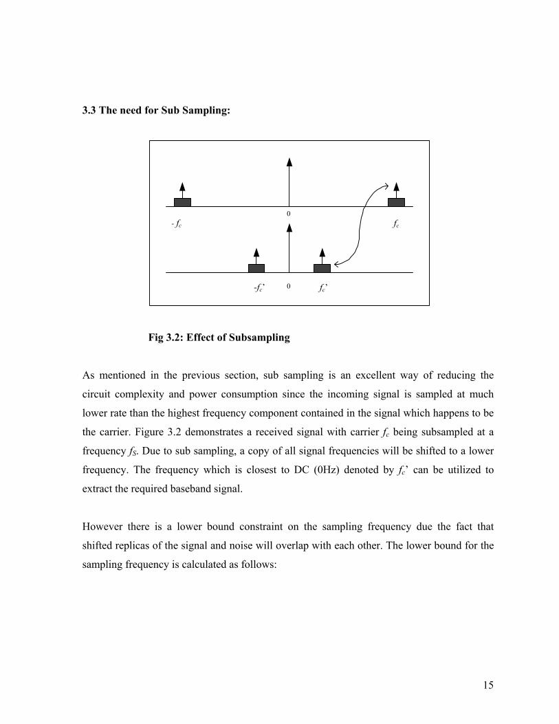
3.3 The need for Sub Sampling:
Fig 3.2: Effect of Subsampling
As mentioned in the previous section, sub sampling is an excellent way of reducing the
circuit complexity and power consumption since the incoming signal is sampled at much
lower rate than the highest frequency component contained in the signal which happens to be
the carrier. Figure 3.2 demonstrates a received signal with carrier fc being subsampled at a
frequency fS. Due to sub sampling, a copy of all signal frequencies will be shifted to a lower
frequency. The frequency which is closest to DC (0Hz) denoted by fc’ can be utilized to
extract the required baseband signal.
However there is a lower bound constraint on the sampling frequency due the fact that
shifted replicas of the signal and noise will overlap with each other. The lower bound for the
sampling frequency is calculated as follows:
0fc - fc
0 fc’ -fc’

16
From sub sampling theory, the frequency component fc’ is given by
fc = α fc’ -(1/2) < α < (1/2)
In order to prevent the out of band noise from aliasing into the signal band, band pass
filtering is done after the amplifier stage. The SAW filter which servers the purpose has a
bandwidth of about fsaw = fc/1000. From the figure, consider the image at – fc’. The noise
within this image should be attenuated before reaching the signal band at fc’. This constraint
is satisfied by
fsaw < 2|α| fc – ∆F ≈ 2|α| fc where ∆F = hfb << fc
fb: data rate of the information source
h: modulation index of FSK
Hence fc > ||2
fsaw
α
It appears that Fs can be selected to down convert fc to DC, but this is not the case. Since the
signal is real valued such a down conversion would make it impossible to distinguish
between fc + ∆F and fc – ∆F and thus prevent detection. Thus fc is shifted to a frequency
closer to DC and then downconverted to DC by multiplying the signal with a complex
exponential exp(-iпn fc’/Fs). If fc’ = ± fS /4, the down conversion reduces to multiplication by
(i, 1, -i, -1) eliminating the need for power hungry multipliers. Further fS has to be an integer
multiple of the data rate in order to facilitate the decimation ratios and reduce power
consumption. Thus fS is chosen to be 1.2 MHz.

17
3.4 Noise effects due to 1 bit quantization:
One bit data processing used in the receiver allows for maximum power savings since the
operation is entirely non-linear. This allows the preceding analog components also to be non-
linear. Non linear analog components like amplifiers and samplers have comparatively
simpler design and hence more power efficient. However the quantization process severely
raises the noise floor as it introduces a large quantization error. Simulation and analytical
results show that an SNR loss of 2 dB is incurred due to one bit quantization. Analytical
treatment follows:
SNRloss =
+−
q
bb
NNE
NE
00loglog10
=
+
0
0log10N
NN q
=
+
01log10
NNq
≈ )10ln(
100N
Nq
The noise power introduced due to B bit quantization is given by,
σ2q =
122 1)--2(B
Since B = 1 in the present case,
σ2q =
121
and Nq = s
q
F
2σ = sF12
1
18
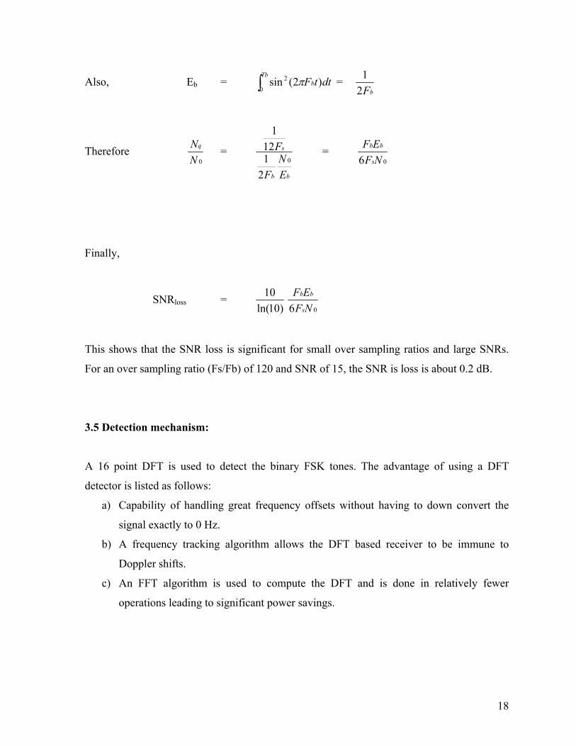
Also, Eb = ∫Tb
b dttF0
2 )2(sin π = bF2
1
Therefore 0N
Nq =
bb
s
EN
F
F0
2112
1
= 06 NF
EFs
bb
Finally,
SNRloss = )10ln(
1006 NF
EFs
bb
This shows that the SNR loss is significant for small over sampling ratios and large SNRs.
For an over sampling ratio (Fs/Fb) of 120 and SNR of 15, the SNR is loss is about 0.2 dB.
3.5 Detection mechanism:
A 16 point DFT is used to detect the binary FSK tones. The advantage of using a DFT
detector is listed as follows:
a) Capability of handling great frequency offsets without having to down convert the
signal exactly to 0 Hz.
b) A frequency tracking algorithm allows the DFT based receiver to be immune to
Doppler shifts.
c) An FFT algorithm is used to compute the DFT and is done in relatively fewer
operations leading to significant power savings.

19
Fig 3.3: FFT Detector
Figure 3.3 shows a block diagram implementation of the FFT detector. The input register to
the FFT engine stores 5 samples from the signal and 11 zeros. It has been proved in [1] that 5
signal samples are sufficient to keep the performance loss below 0.25 dB. The contents of the
register are then fed into the FFT engine. The output of the FFT is a bank of 16 values
referred to as ‘bins’. Each of these bins represents the energy content of the signal in
different frequency intervals. Data detection is done by analyzing the 16 bins. One out of the
16 bins is regarded to be the ‘decision bin’. The output of the decision bin is compared with a
known threshold value using a comparator circuit. Decision is in favor of symbol 1 if the
value of the ‘decision bin’ is greater than the threshold value; else decision is in favor of
symbol 0.
X(5) X(4) X(3) X(2) X(1) 0 0 0 0 0 0 0 0 0 0 0
16 POINTFFT
16 15 14 13 12 11 10 9 8 7 6 5 4 3 2 1
DECISIONBLOCK
Data Samples
Data from MUX
INPUT REGISTER
FFT BIN REGISTER

20
Fig 3.4: Control System block diagram
16:1MUX
DELAY 1 DELAY 2BIN RESBLOCK
TEMP_BINCOUNTER
DEMODBLOCK
CONTROLCOUNTER
CLKCOUNTER
3:1MUX
tem
p_bi
n
bin_out
enable
clk_count
clk
bin_out
enable
en_temp_bin
bin 1
bin 2
bin 16
clk_10k
clk_1k
clk_100
checkenable
temp_bin
en_temp_bin
sig_out
clk
en_t
emp_
bin
clk
demod

21
3.6 Control System:
Figure 3.4 depicts the block diagram of the control circuit. The output of the DFT
detector is captured by a 16 to 1 multiplexer. The purpose of the control circuit is to
determine the “decision bin” out of the 16 bins and to decide the symbol rate. In order to
facilitate bin resolution and data detection a pilot signal is first transmitted from the
transmitter which consists of a series of alternate ones and zeros. To start with, the very
first bin is selected and the data rate is assumed to be 10kbps. The output of the 16:1
MUX is passed through two registers each serving the purpose of delaying the data by
one clock cycle. This is done so that two subsequent symbols can be compared with each
other. The bin resolution block compares the values of the registers DELAY1 and
DELAY2 with a threshold value. The following decision algorithm is used:
Current bin = Decision bin if DELAY1 < Threshold value < DELAY2 or
DELAY2 < Threshold value < DELAY1
The threshold value in the bin resolution can be adjusted allowing for variations in the
output of the DFT block. If decision fails on the current bin then the next bin is selected
by incrementing the ‘temp_bin’ line. This process is repeated until a decision bin is found
with the present clock rate. Once the value of ‘temp_bin’ reaches 16 and still a “decision
bin” hasn’t been found, it implies that the data rate is different is from the one assumed.
Hence the clock rate is reduced to 1kbps and then the process is repeated starting with the
first bin. The ‘CONTROL COUNTER’ block is used to assert the ‘check’ signal which
enables the “BIN_RES BLOCK’. After obtaining the right decision bin, control is
transferred to the demodulation block which takes care of converting the output of the
DFT to binary symbols.
22
CHAPTER 4
SIMULINK MODEL
4.1 Introduction to SIMULINK:
MATLAB or “Matrix laboratory” is one of the most popular technical computing
environments today that provides mathematical and engineering functions for system
simulations, data analysis and algorithm development. MATLAB operates as an
interactive programming environment and has support for graphical output to supplement
numerical results. SIMULINK is a simulation and prototyping environment, part of
MATLAB for modeling, simulating and analyzing dynamic systems. SIMULINK
provides a block diagram interface that is built on the core MATLAB numeric, graphics,
and programming functionality. MATLAB has a collection of highly optimized
application specific functions called “toolboxes”. Toolbox functions are built in
MATLAB language and can be easily incorporated into a MATLAB program, viewed
and modified. “Block sets” are collections of application specific blocks built on the
functionality of toolboxes and can be directly included in SIMULINK models.
SIMULINK uses a graphical user interface (GUI) for solving process simulations. Instead
of writing MATLAB code, we simply connect the necessary “icons'” together to
construct the block diagram. SIMULINK is an icon-driven state of the art dynamic
simulation package that allows the user to specify a block diagram representation of a
dynamic process. Assorted sections of the block diagram are represented by icons which
are available via various "windows" that the user opens (through double clicking on the
icon). The block diagram is composed of icons representing different sections of the
process (inputs, state-space models, transfer functions, outputs, etc.) and connections
between the icons (which are made by "drawing" a line connecting the icons). Once the
block diagram is "built", one has to specify the parameters in the various blocks, for
example the gain of a transfer function. Once these parameters are specified, then the user
can simulate the model.

23
Fig 4.1: SIMULINK model of the FSK receiver
TRANSMITTER
RECEVIER

24
4.2 SIMULINK model of the receiver:
Fig 4.1 shows the block diagram of the FSK receiver modeled in SIMULINK. Obviously a
receiver cannot be tested without a transmitter indicating the presence of a transmitter and an
AWGN channel in the block diagram. The transmitter is modeled with a Bernoulli random
number generator as its information source. The random generator is configured to output
either a one or a zero with a specific probability and at a rate of 10kbps. There are two signal
sources acting as the two carriers of BFSK. One of the sources operates with a frequency of
437.1 MHz while the other operates at 437.12 MHz. The tone separation is thus 20 KHz.
Two product modulators are used, the upper one for modulating symbol 1 and the lower one
for symbol zero. Finally outputs of the modulators are summed to simulate a BFSK signal
with an information rate of 10kbps. The signal is passed through an additive white Gaussian
noise channel (AWGN) to add white noise to the transmitted signal. This completes
modeling the transmitter and the channel.
The receiver part of the block diagram starts with a sign block that basically functions like a
1-bit A/D converter. The sign block outputs a one if the input value is greater than zero else a
negative one if the input is less than zero. The convention is, symbol one is represented by
value one while symbol zero with value negative one. This is done in order to distinguish
symbol zero from the value zero. The sign block is operated at a sampling rate of 1.2 MHz.
The output of the sign block is down converted to base band by multiplying the signal with a
complex exponential. As we have discussed before, complex multiplication is reduced to
multiplication with 1, i,-1 and –i by proper choice of sampling frequencies. 1 and -1
represents the real part while i and –i represents the imaginary part. Since the quantities are
complex in nature, the real part and the imaginary part should be processed separately.
Consequently the data path this point onwards branches out to two paths; the real path and
the imaginary part as witnessed in the diagram. The upper branch denotes the real part with
the received signal being multiplied by cos(Πn/2N) and the lower branch is the imaginary
part being multiplied by sin(Πn/2N). The processing blocks for real data and imaginary data
are the same. The down converted signal is now decimated by 24 to reduce the data rate to
25
50kbps. We now have a signal that can be processed by the FFT detector. As we have
discussed before, the FFT block uses only 5 samples of the signal for DFT computations. The
rest 11 inputs to the detector are zeros. This process results in an additional decimation of the
data rate by 5, bringing down the rate to 10kbps which should be the final data rate. As we
can see there is an inherent timing synchronization in the design resulting from proper choice
of the sampling frequency of the A/D converter and the decimation ratios. For lesser data
rates such as 1kpbs and 100bps, additional stages of decimation are required. For instance,
for a data rate of 1kpbs, the 50kpbs signal is decimated by 10 to reduce the rate to 5kpbs.
This signal incurs an additional decimation of 5 from FFT processing finally yielding a data
rate of 1kpbs.
The SIMULINK model of the receiver does not include the FFT detector block as well as the
control circuit block. We found it more convenient to capture the output of the decimated
signal to a workspace (which basically stores all the data values as a matrix) and then writing
a MATLAB script to apply the FFT on the captured data. The program also does the
additional task of stripping the first five bits from the data and padding the bits with eleven
zeros and feeding them to the FFT algorithm. The MATLAB script is included in the
Appendix for reference. Generally, it is very difficult to model a control circuit in
SIMULINK. Hence we decided that the easiest way was to write a VERILOG or VHDL
program capturing the functional or gate level description of the control circuit and then
simulating it. Since the final objective is to reduce the entire receiver model to hardware, this
method saves an additional step of converting the SIMULINK model to a VHDL/VERILOG
model. The control block which was explained in the previous chapter is written in VHDL
and is included in the Appendix for reference.

26
4.3 SIMULATIONS
Fig 4.2: Transmitted waveform and Received Digitized waveform
We simulated the SIMULINK model for all the three data rates and found that the model was
performing as expected. The wave forms obtained at various points in the design when the
model is run with a bit rate of 10kpbs are indicated in this section. The simulation is run for
0.02 seconds so that 200 symbols are emitted by the Bernoulli source. Figure 4.2 shows a
section of three different waveforms. The first waveform is the output of the FSK transmitter.
The first half of the waveform represents symbol 1 and the second half represents symbol 0.
The frequency of the signal associated with symbol 1 is 473.12 MHz and the frequency of
symbol 0 is 473.1 MHz. The second waveform is the result of the FSK waveform being
passed though the additive white Gaussian channel with an SNR of 5db and a noise power of
100mW. As we can see, the transmitted signal is highly corrupted by noise in the channel.
This signal is input to the 1-bit A/D converter of the receiver which basically converts the
received signal to a rectangular waveform as witnessed in waveform 3. We can also see a
clear distinction between symbol 0 and symbol 1 in their frequency representations.
SYMBOL 1 SYMBOL 0
FSK WAVE
OUPUT OF AWGN CHANNEL
OUTPUT OF 1-BIT A/D

27
Fig 4.3: Down conversion waveforms
Figure 4.3 shows the waveforms resulting from the down conversion operation. These
waveforms are specific to data processing in the real path. The first waveform is the 1 bit
digitized waveform from the A/D converter. The second waveform is the cosine waveform
that alternates between 1 and -1 with 0 interspersed. The cosine signal servers the purpose of
the in-phase function required for real part multiplication. The third waveform is real part of
the down converted wave which is the product of the first and the second waveforms.
SYMBOL 0 SYMBOL 1
1 BIT DIGITIZED SIGNAL
COSINE WAVEFORM FOR REAL PART OF DOWNCONVERSION
DOWNCONVERTED WAVE

28
Fig 4.4: Decimated waveform
Figure 4.4 depicts the results of data rate decimation. The first waveform is the down
converted wave which we have seen before, and the second waveform is the result of
decimation by the order 24. We can see that the decimated waveform has a clear distinction
between the symbols 0 and 1.
SYMBOL 0 SYMBOL 1
DOWNCONVERTED WAVE
WAVE DECIMATED BY 24
29
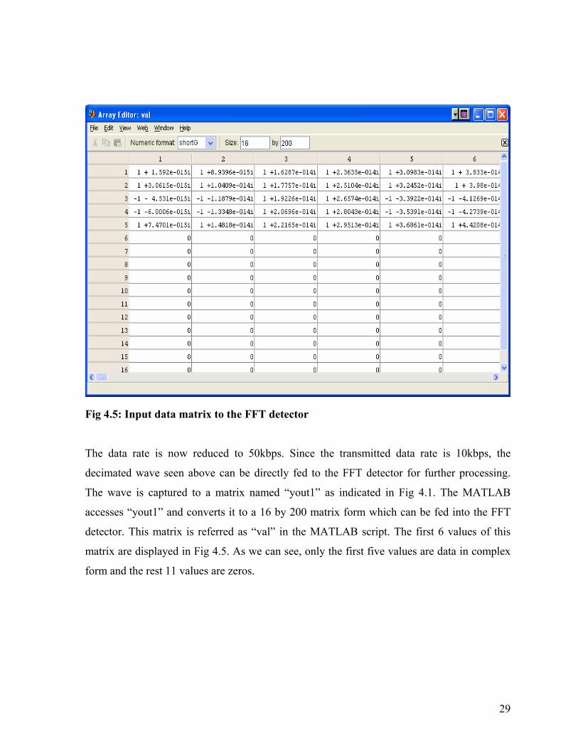
Fig 4.5: Input data matrix to the FFT detector
The data rate is now reduced to 50kbps. Since the transmitted data rate is 10kbps, the
decimated wave seen above can be directly fed to the FFT detector for further processing.
The wave is captured to a matrix named “yout1” as indicated in Fig 4.1. The MATLAB
accesses “yout1” and converts it to a 16 by 200 matrix form which can be fed into the FFT
detector. This matrix is referred as “val” in the MATLAB script. The first 6 values of this
matrix are displayed in Fig 4.5. As we can see, only the first five values are data in complex
form and the rest 11 values are zeros.

30
Fig 4.6: Output data matrix after FFT computation
The formatted data as seen in the matrix “val” is fed to the FFT detector which is basically
implemented by invoking the MATLAB “fft” inbuilt function. Fig 4.6 displays the absolute
value of the output of the FFT operation stored in a matrix named “res1”. The column
numbers represent the symbol instants and the rows represent the 16 bin output for each
symbol. The first eleven symbols transmitted by the Bernoulli source are 1, 1, 0, 0, 1, 1, 1, 1,
0, 0 and 0. With theses symbols in view, we can see from fig 4.6 that there are quite a few
bins which can be regarded as a “decision bin” for symbol detection. We select bin number 5
to be our decision bin and set a threshold value of 2. Hence the decision algorithm now
becomes,
Symbol = 1 if bin (5) > 2
0 if bin (5) < 2

31
Fig 4.7: Receiver output after symbol detection
Fig 4.8: Output of the Bernoulli transmitter

32
Fig 4.7 shows the final detected waveform plotted in MATLAB and fig 4.8 shows the input
waveform. As we can see, the transmitted waveform and the detected waveform match with
each other.
Fig 4.9: FFT detector output after Doppler shift of 5 KHz
To test the receiver for Doppler invariance, we increased the carrier frequencies of the
transmitter by 5 KHz and ran the model. Fig 4.9 displays the output of the FFT detector for
the first eleven time instants. As we can see, the decision bin is no longer bin 5 and is
displaced to a different bin. Then, the task is to change the decision bin from bin 5 to another
suitable bin. In this case we choose, bin 8. A frequency tracking algorithm will help keep
track of the changes in magnitude of the decision bin. As we see a decrease in the magnitude
of the decision bin, we also see a proportional increase in the magnitude of the bin adjacent
to the decision bin. Thus the function of the frequency tracking algorithm is to
increment/decrement the bin number when the decision bin magnitude falls below a certain
level.

33
4.4 VERIFICATION
In order to test whether the receiver was working, we sent a string of 10 bits from the
transmitter and observed the bit string at the receiver after detection. The test case is give
below,
TEST CASE FOR 10KBPS DATA RATE
TRANSMITTED BIT SEQUENCE : 1,0,1,1,1,0,0,0,0,1
CARRIER FREQUENCY 1 : 473.12MHZ
CARRIER FREQUENCY 2 : 473.1MHZ
INPUT SIGNAL : 100mW
SNR : 15dB
DATA OBSERVED AT THE RECEIVER
RECEIVED BIT SEQUENCE : 1,0,1,1,1,0,0,0,0,1
DECISION BIN : BIN 7
MAXIMUM VALUE (BIT 1) : 3.17
MINIMUM VALUE (BIT 0) : 0.566
THRESHOLD VALUE : 2
These results imply that the receiver is working as expected. Similar tests were conducted for
data rates of 1kbps and 100bps and found that the receiver was working properly.
4.4.1 Receiver Performance to Doppler Shifts
We tested the receiver for Doppler changes in frequency by varying the frequency of the
transmitted signal by different proportions. We found that the receiver was working
satisfactorily for Doppler shifts up to 10 KHz. Table 4.1 shows the simulation results.
Transmitted data rate : 10kbps
Decision bin without Doppler shift : Bin 8

34
CHANGE IN
FREQUENCY 100HZ 200HZ 500HZ 1KHZ 1.5KHZ 3KHZ
DECISION
BIN 8 8 7 7 6 6
Table 4.1: Performance of the receiver to Doppler Shift
Similar tests were conducted for data rates of 1kbps and 100bps and found satisfactory
performance.
4.4.2 Receiver BER Performance
Table 4.2: BER performance of the receiver
We tested the model for a variety of noise conditions by varying the SNR of the transmitted
signal in the AWGN channel. We set the input signal power at a constant 100mW. Table 4.2
displays the results obtained for different values of SNR. The BER was measured by
transmitting 1000 information symbols at the transmitter end and measured the no of
10KBPS 1KBPS 100BPS SNR
(dB) DETECTION
ERRORS BER
DETECTION
ERRORS BER
DETECTION
ERRORS BER
1 290 0.29 135 0.135 130 0.13
5 250 0.25 110 0.11 108 0.108
10 120 0.12 85 0.085 80 0.08
15 1 0.001 0 10e-5 0 10e-5
20 0 ≈0 0 ≈0 0 ≈0
25 0 ≈0 0 ≈0 0 ≈0

35
symbols that were detected erroneously. After comparing these results with the BER
performance of an optimal un-coded non coherent FSK receiver, we found that the FFT
based receiver has a performance degradation of approximately 2.5 db at a BER of 10e-3.
The difference in performance is lesser for better BER. The results also indicate consistency
in the performance of the receiver to the three data rates.
Figure 4.10 displays a logarithmic plot of BER v/s SNR. The y axis corresponds to BER
values and is in logarithmic scale while the x axis corresponds to SNR values (dB) and is in
linear scale.
Fig 4.10: BER plot for the three data rates

36
4.4.3 Receiver performance to variations in A/D clock
Original Clock Frequency : 1.2 MHz
Data rate : 10 kbps
SNR : 15 dB
Table 4.3: Receiver performance to clock variation at A/D converter
We tested the receiver by varying the clock frequency by small amounts at the A/D
converter. Table 4.3 indicates the simulation results obtained. Such frequency variations are
restricted to ± 0.5% of the original clock rate. As we can see, the performance of the receiver
degrades as the variation in clock frequency increases and is highest at 0.5% variation.
Frequency Variation (%) BER
0.1 0.008
0.2 0.012
0.3 0.017
0.4 0.024
0.5 0.036
37
CHAPTER 5
XINLINX IMPLEMENTATION OF THE RECEIVER
5.1 Introduction to System Generation in XILINX
The receiver model developed in SIMULINK is useful to validate the functionality of the
receiver design at a system level. In order to get a power estimate of the receiver, the
SIMULINK model has to be reduced to hardware. As mentioned before, SIMULINK’s
XILINX block set allows us to develop a XILINX hardware model of the receiver using the
XILINX building blocks. This process basically reduces to translation of the SIMULINK
model to a XILINX model provided a one to one correspondence exists between each and
every block. The hardware model is developed and tested in SIMULINK and the system
generator tools of XILINX is used to synthesize the model by generating .bit file targeted to a
particular XILINX FPGA. A .bit file contains all the configuration information defining all
the internal logic and interconnections in the FPGA.
The System Generator in XILINX is a very convenient method for electronic designs to be
created, tested, and translated into hardware for XILINX FPGAs. The tool extends
SIMULINK to support bit and cycle accurate system level simulation, and automatic code
generation for XILINX FPGAs. System Generator co-simulation interfaces extend
SIMULINK to incorporate FPGA hardware and HDL simulation into the system-level
environment as naturally as other library blocks. System Generator presents a high level and
abstract view of the design, but also exposes key features in the underlying silicon, making it
possible to build extremely high-performance FPGA implementations.

38
System Generator designs are built and simulated within the SIMULINK block editor. Each
block produces results that make sense for the setting in which it is used. For example, a
multiplier whose inputs are signed fixed point numbers produces a signed result having an
appropriate width and binary point position. Signal types are propagated automatically, so
when one block is updated, System Generator adjusts downstream blocks accordingly.
5.1.1 System Generation DESIGN FLOW
Fig 5.1: XILINX System Generation Design Flow
Figure 5.1 illustrates the various processes involved in transforming a high level design
created in SIMULINK to a low level FGPA implementation. A brief description of all the
steps follows:
STEP1: A high level system design of the model is developed and tested in
MATLAB/SIMULINK using the XILINX block set provided in SIMULINK.
SYSTEM MODELING IN MATLAB/SIMULINK
XILINX SYSTEM GENERATOR
HDL SYNTHESIS(XILINX XST, SYNPLIFY PRO,MENTOR GRAPHICS)
SIMULATION(MENTOR GRAPHICS FPGA ADVANTAGE)
FPGA IMPLEMENTATION(XILINX ISE)
STEP 1
STEP 2
STEP 3
STEP 4
STEP 5

39
STEP2: System Generation is invoked in SIMULINK using the “XILINX System
Generation” icon in the SIMULINK model. This process generates VHDL code for
all the XILINX blocks in the SIMULINK design. FPGA designs are generated using
XILINX’s LogiCOREs to produce the most efficient implementation.
STEP3: The VHDL design is synthesized to FPGA using one of the three most popular
synthesis tools namely XILINX’s XST, SYNPLICITY’s SYNPLIFY PRO and
MENTOR GRAPHICS’s FPGA Advantage.
STEP4: This step is optional and can be used to simulate the VHDL design using MENTOR
GRAPHICS’s FPGA Advantage. A test bench and data vectors can be created using
the System Generator. The data vectors represent the input and the expected outputs
as simulated in the SIMULINK design.
STEP5: The synthesized design is loaded into a XILINX FPGA using place and route tools
of XILINX’s ISE.
5.2 XILINX Model: Top level system
Fig 5.2: XILINX Model top level system diagram
TRANSMITTER AND CHANNEL IMPLEMTEDIN SIMULINK
RECEIVER IMPLENTED USING XILINX BLOCK SET

40
The XLINX model looks pretty much alike the SIMULINK model as we can see from fig
5.2. The transmitter and channel blocks are modeled using the SIMULINK block set while
the receiver is modeled using the XILINX block set and included in “Subsystem2”. A
provision is made to generate the pilot sequence for an initial period of 0.01 sec in the
transmitter block. As mentioned before, the pilot sequence consists of a series of alternating
0s and 1s and is used to facilitate the control system of the receiver to detect the transmitted
data rate and to configure one of the FFT bins as the “decision bin”. The pilot signal needs to
be transmitted every time the data rate changes, as this is the only way the receiver can detect
a change in the transmitted data rate.
Fig 5.3: Receiver Model implemented in XILINX

41
The subsystem2 seen in Fig 5.2 is composed to two subsystems demarcated mainly due to
their functionalities. The first subsystem takes care of down conversion of the digitized signal
and decimation. The second subsystem takes care of FFT detection. As we can see from Fig
5.3, the red block named “System Generator” is used to translate the XILINX design to
XILINX hardware targeted to a particular FPGA. The System Generator block has various
parameters that can be set to generate XILINX hardware for a specific device and speed.
Some of these parameters are:
a) Product Family. E.g. SPARTAN, VIRTEX, VIRTEX2 etc
b) Package. E.g. fg676, bg575 etc
c) Synthesis tool. E.g. XST, SYNPLIFY etc
d) FPGA System clock period
5.3 XILINX MODEL: Down conversion
Fig 5.4: XILINX hardware model of the Down conversion operation

42
Figure 5.4 depicts the hardware design of the down conversion sub system of the receiver.
All the blocks used in the design are provided in the XILINX block set and can be readily
synthesized to XILINX hardware. The input signal to the block is the 1 bit digitized signal
from the A/D converter. The input signal has to pass though the “Gateway In” block that
converts values of type “double” to the “XILINX fixed point” type. The number of bits for
each data value is 20 and the data type is signed (2s complement). The binary point of the
data is located at 0. As we can see, there exist two identical data paths in the design. The first
one represents the real path and the second one represents the imaginary part. A direct digital
synthesizer (DDS) is used to generate the required sine and cosine waveforms for down
conversion. Then, the signal is down sampled by 24, 10 and 10 and all the outputs are fed
into a 3:1 MUX. The select line of this MUX is controlled by the control system as
mentioned before. The output of the MUX is passed to a serial to parallel converter which
takes 5 serial 20 bit data values and converts it into one data value of bit length 100 which is
basically a concatenation of all the data values. This is done in order to stack five signal
samples per symbol for FFT detection. The parallel bit is sliced back into 20 bits each using
the “slice” blocks. Finally the output of the “slice” block is type converted to signed (2s
complement) data type and fed into the FFT detector.

43
5.4 XILINX Model: FFT Detector
Fig 5.5: XILINX Hardware Model of the FFT Detector
As mentioned before, the FFT detector is modeled based on the algorithm proposed by
Bertazzoni [2]. Figure 5.5 depicts the XILINX hardware model of the FFT detector which
consists of various interconnected subsystems. Each subsystem has two kinds of inputs; real
and imaginary. The purpose of these subsystems is to add and shift the complex data
according to the FFT algorithm and thus implementing the CORDIC algorithm.

44
Fig 5.6: Subsystem to implement the sum of real and imaginary parts for FFT
computation

45
Fig 5.7: Subsystem to implement a rotation of 45o for FFT computation
Fig 5.8: Subsystem to implement a rotation of 22.5o for FFT computation

46
Figures 5.6, 5.7 and 5.8 represent the internal hardware block diagram of the subsystems
used in the FFT detector based on the CORDIC algorithm. Figure 5.6 shows the hardware
block used for summing the real and imaginary parts of complex input data. The hardware
depicted in figures 5.7 and 5.8 are used to rotate a complex vector by angles 45o and 22.5o
respectively as proposed in [2].
Fig 5.9: Waveforms displayed after symbol detection
The output of the FFT detector is fed to the control system that takes care of symbol decision
based on the threshold value. The XILINX model was tested in SIMULINK for a data rate of
10kbps in presence of the AWGN channel. Figure 5.9 displays the results of the detected
waveform. The top waveform is the transmitted data from the Bernoulli random generator.
The bottom wave is the detected wave by the receiver. The transmitted and the received
waves match with each other indicating successful operation of the XILINX hardware model
of the receiver. Note a delay of one clock cycle in the received waveform.

47
5.5 Synthesis to XILINX FPGA
We synthesized the XILINX hardware model to a XILINX FPGA using the system generator
tool. The product family used was Virtex2, deice used was xc2v1500 (anticipating around
1000 million gates) and the XILINX system clock period was set to 100ns. The model was
synthesized successfully and following is timing report as indicated in the synthesis report of
XILINX:
Timing Summary:
---------------
Speed Grade: -6
Minimum period: 6.841ns (Maximum Frequency: 146.178MHz)
Minimum input arrival time before clock (Critical Path Delay): 4.282ns
Following is the MAP report obtained from XILINX for the receiver model indicating the
total gate count and number of slices used in the FPGA.
Design Summary
--------------
Number of Slices: 2,633 out of 7,680 34%
Total equivalent gate count for design: 85,456
We ran XPOWER utility of XILINX and found that the total power usage of the receiver is
280mW.
48
CHAPTER 6
CONCLUSION AND FUTURE WORK
We have successfully designed and simulated a low power BFSK receiver intended for future
deep space missions. The receiver is implemented with a 16 point FFT detector for Doppler
invariance and tests show that frequency shifts of up to 10 KHz are tolerated by the receiver.
We have tested the receiver for data rates of 10kbps, 1kbps and 100bps. The worst case BER
performance of the receiver is about 2.5db less than the optimal non coherent FSK receiver at
a BER of 10E-3 and data rate of 10kbps. We have successfully understood the design flow of
XILINX system generation. The SIMULINK model of the receiver is used to develop a
XILINX model of the receiver and synthesized to VIRTEX-2 FPGA using system generation
and XILINX ISE tools. Power estimation of the receiver as per the XPOWER utility of
XILINX is 280mW.
6.1 Future Work
The power consumption of the receiver can be further reduced by making a few design
modifications. The FFT Detector can be implemented using a radix-4 FFT algorithm instead
of the existing radix-2 algorithm for better power and space efficiency. The hardware
multiplier and the digital frequency synthesizer at the down conversion stage could be
substituted by simpler circuits. A frequency tracking circuit can be implemented in the
control system to track the change in decision bins due to Doppler shifts.

49
BIBLIOGRAPHY
[1] E. Grayver and B. Daneshrad, “A low power all digital FSK receiver for space
applications”, IEEE Trans. Communications, Volume: 49 Issue: 5, May 2001,
Page(s): 911 -921
[2] S. Bertazzoni et al., “16-point high speed (I)FFT for OFDM modulation”, Proceedings of
the 1998 IEEE International Symposium on Circuits and Systems, Volume: 5, 31 May-3 June
1998, Page(s): 210 -212.
[3] J. G. Proakis and D. G. Manolakis, Digital Signal Processing. Englewood Cliffs, NJ:
Prentice-Hall, 1997.
[4] S. Hara, A.Wannasarnmaytha, Y. Tsuchida and N. Morinaga, “A novel FSK
demodulation method using short-time DFT analysis for LEO satellite communication
systems”, IEEE Trans. Veh. Technol., Volume: 46, Aug. 1997, Page(s) 625–633.
[5] E. Grayver and B. Daneshrad, “VLSI implementation of a 100-µW multirate FSK
receiver”, IEEE J. Solid-State Circuits, Volume: 36 Issue: 11, Nov. 2001,
Page(s): 1821 -1828.
[6] Bernard Sklar, Digital Communication, Fundamentals and Applications. Englewood
Cliffs, NJ: Prentice-Hall, 1988.
[7] Martin. S. Roden, Digital Communication System Design. Englewood Cliffs, NJ:
Prentice-Hall, 1988.
[8] H.-C. Liu, J. S. Min and H. Samueli, “A low-power baseband receiver IC for frequency-
hopped spread spectrum communications”, IEEE J. Solid-State Circuits, Volume: 31, March
1996, Page(s) 384–394.
[9] E. Grayver and B. Daneshrad, “Low power, area efficient programmable filter and
variable rate decimator”, The 2000 IEEE International Symposium on Circuits and Systems,
Volume: 5, 28-31 May 2000, Page(s): 341 -344.
[10] M. K. Lee, K. W. Shin, J. K. Lee, “A VLSI Array processor for 16-point FFT”, IEEE J.
Solid-State Circuits, Volume: 26, No. 9, Nov. 1996, Page(s): 1286-1292.

50
APPENDIX
1. MATLAB script for FFT computation and symbol decision
% Strip 5 data values from the received signal compute = 1 if compute == 1 n_symbols = 1000 count = 1 for n = 1:n_symbols for j = 1:5 val(j,n) = complex(yout1(count+j,2),yout1(count+j,1)) end count = count + 5 end %Pad the remaining 11 values with zeros for n = 1:n_symbols for j = 6:16 val(j,n) = 0 end end % Compute the FFT res = fft(val,16); res1 = abs(res); end % Symbol decision threshold = 2 decision_bin = 7 for n = 1:n_symbols if res1(decision_bin,n) > threshold wave(n) = 1 else wave(n) = 0 end end

51
%Compute error for BER analysis error = 0 for n = 1:n_symbols if wave(n) ~= yout4(n) error = error +1 end end

52
2. VHDL code implementing the control system for bin resolution and rate detection
library ieee; use ieee.std_logic_1164.all; use ieee.numeric_std.all; -- Definition of entity called control Entity control is port(bin1,bin2,bin3,bin4,bin5,bin6,bin7,bin8,bin9,bin10,bin11,bin12,bin13,bin14,bin15, Bin 16 : in std_logic_vector(19 downto 0); clk_10k, clk_1k, clk_100, rst : in std_logic; rate : out std_logic_vector(0 to 1); sig_out : out std_logic); end control; -- Architecture definition of the entity control architecture structure of control is type states is (binresolution, demodulation); signal currentstate, nextstate : states; signal bin_val1, bin_val2, bin_out : std_logic_vector(19 downto 0); signal count, count_clk : unsigned(0 to 1) := "00"; signal temp_bin : unsigned(0 to 3) := "0000"; signal clk : std_logic := clk_10k; signal demod, enable, en_temp_bin, check : std_logic; begin -- Select one of the three clocks SELECTCLK : process(clk_10k, clk_1k, clk_100) begin case count_clk is when "00" => rate <= "00"; clk <= clk_10k; when "01" => rate <= "01"; clk <= clk_1k; when "10" => rate <= "10"; clk <= clk_100; when others => rate <= "00"; clk <= clk_10k; end case; end process;

53
-- State register STREG : process(clk, rst) begin if rst = '1' then currentstate <= binresolution; elsif rising_edge(clk) then currentstate <= nextstate; end if; end process; -- Select one of the 16 bins BINMUX : process(temp_bin,bin1, bin2, bin3, bin4, bin5, bin6, bin7, bin8, bin9, bin10, bin11, bin12, bin13, bin14, bin15, bin16) begin case temp_bin is when "0000" => bin_out <= bin1; when "0001" => bin_out <= bin2; when "0010" => bin_out <= bin3; when "0011" => bin_out <= bin4; when "0100" => bin_out <= bin5; when "0101" => bin_out <= bin6; when "0110" => bin_out <= bin7; when "0111" => bin_out <= bin8; when "1000" => bin_out <= bin9; when "1001" => bin_out <= bin10; when "1010" => bin_out <= bin11; when "1011" => bin_out <= bin12; when "1100" => bin_out <= bin13; when "1101" => bin_out <= bin14;

54
when "1110" => bin_out <= bin15; when "1111" => bin_out <= bin16; when others => bin_out <= bin_out; end case; end process; -- Bin decision STTRANS : process(currentstate, check) begin case currentstate is when binresolution => demod <= '0'; enable <= '1'; en_temp_bin <= '0'; if check = '1' then
if ((signed(bin_val1) > 7 and signed(bin_val2) <-7 ) or (signed(bin_val2) > 7 and signed(bin_val1) < -7 )) then
nextstate <= demodulation; enable <= '0'; en_temp_bin <= '0'; else enable <= '1'; en_temp_bin <= '1'; end if; end if; when demodulation => demod <= '1'; end case; end process; -- count register MYCOUNTER : process(clk, enable, rst) begin if rst = '1' then count <= "00"; elsif rising_edge(clk) and enable = '1' then count <= count + 1; else count <= count; end if; end process;

55
-- Registers for storing two successive samples of a particular bin BINVAL : process(clk, enable, rst) begin if rst = '1' then bin_val1 <= "00000000000000000000"; bin_val2 <= "00000000000000000000"; elsif rising_edge(clk) and enable = '1' then bin_val1 <= bin_out; bin_val2 <= bin_val1; else bin_val1 <= bin_val1; bin_val2 <= bin_val2; end if; end process; -- The check signal CHECKSIG : process(clk, rst, enable, count) begin if rst = '1' then check <= '0'; elsif rising_edge(clk) and count = "11" then check <= '1'; else check <= check; end if; end process; -- The temp_bin register for the select line of 16:1 Mux TEMPBIN : process(clk, en_temp_bin, rst) begin if rst = '1' then temp_bin <= "0000"; count_clk <= "00"; elsif rising_edge(clk) and en_temp_bin = '1' then if temp_bin = "1111" then count_clk <= count_clk + 1; end if; temp_bin <= temp_bin + 1; end if; end process;

56
-- The demodulation proces STDEMOD : process(clk, demod) begin if rising_edge(clk) and demod = '1' then if signed(bin_out) > 7 then sig_out <= '1'; else sig_out <= '0'; end if; end if; end process; end structure;