Embed Size (px)
Citation preview
• SoC (System on a Chip) designs are now becoming very prevalent because of the design and IP reuse, and to enable design implementation across multiple groups and geographies. This introduces a lot more challenges at the full chip integration level which includes checking for design-methodology consistency, connectivity of complex IPs that may have mixed signal behavior, chiplet connectivity that includes test and functional signals.
• SoC designs follow a hierarchical chip implementation approach to enable physical design and module level verifi cation. Generally because of the complexity of the module level verifi cation a lot of the verifi cation cycles are spent at that level, with very little attention to the full chip view early in the design phase. With technology node shrinking, more of the physical design challenges are at the full chip level, and nailing down the full chip and inter block connectivity becomes a critical element for route resource allocation and timing. So there is a need to validate the design intent which supplements simulation based verifi cation.
• This paper will describe a structural SoC connectivity based solution using Atrenta’s SpyGlass tool to validate the design-intent in a multi-million ASIC design fl ow used in a high-end networking product. A few design examples will be used to demonstrate the power and scope of such a validation fl ow. The simplic-ity and abstraction of the rule deck enables easy portability of methodology across design groups/product lines. Future enhancements with respect to preamble support will be discussed. We conclude with a set of recommendations for managing the mix of connectivity based validation and dynamic techniques during product development.
Capturing the Design-Intent• Multitude of IPs from different sources• Validating Design Methodology consistency across blocks
Supplementing Simulation Based Verifi cation• Quickly fi nd basic bugs, mixed-signal block connectivity• Regression support• Detailed reporting for independent analysis
The Feature Support• Abstracted connectivity check - spec match• Value, Path, Structure Check• Quick synthesis & Tcl support for custom checks
Goal• Static verifi cation of Memory BIST connectivity for all memories in a design – consistent with a design methodology
Challenges• ~4000 physical memory cuts of different types (SRAM, TCAMs, RFs..)• ~100 Physical design blocks, done across geographies• Constant design changes requiring memory modifi cations
Detailed Validation Requirements• Consistent integration fl ow across memories (including custom point–point checks)• Extraction of design elements prior to the execution of checks – supports automation and regress-ability• Be able to look for connectivity to a certain type of registers (by instance name)• Ability to trace through combo and check for uniqueness of logic implemented• Ability to fl ag unwanted logic and pipelining
Runtime• Less than 20 mins of runtime for a million gate design• Dashboarding support
Reporting Structure• Easy text based reporting• GUI based design analysis
Examples of violation types• Pipelining on the connection path which violates handshake requirements• Wrong tie-off values during incremental memory changes• Missing memory connectivity at different levels of hierarchy
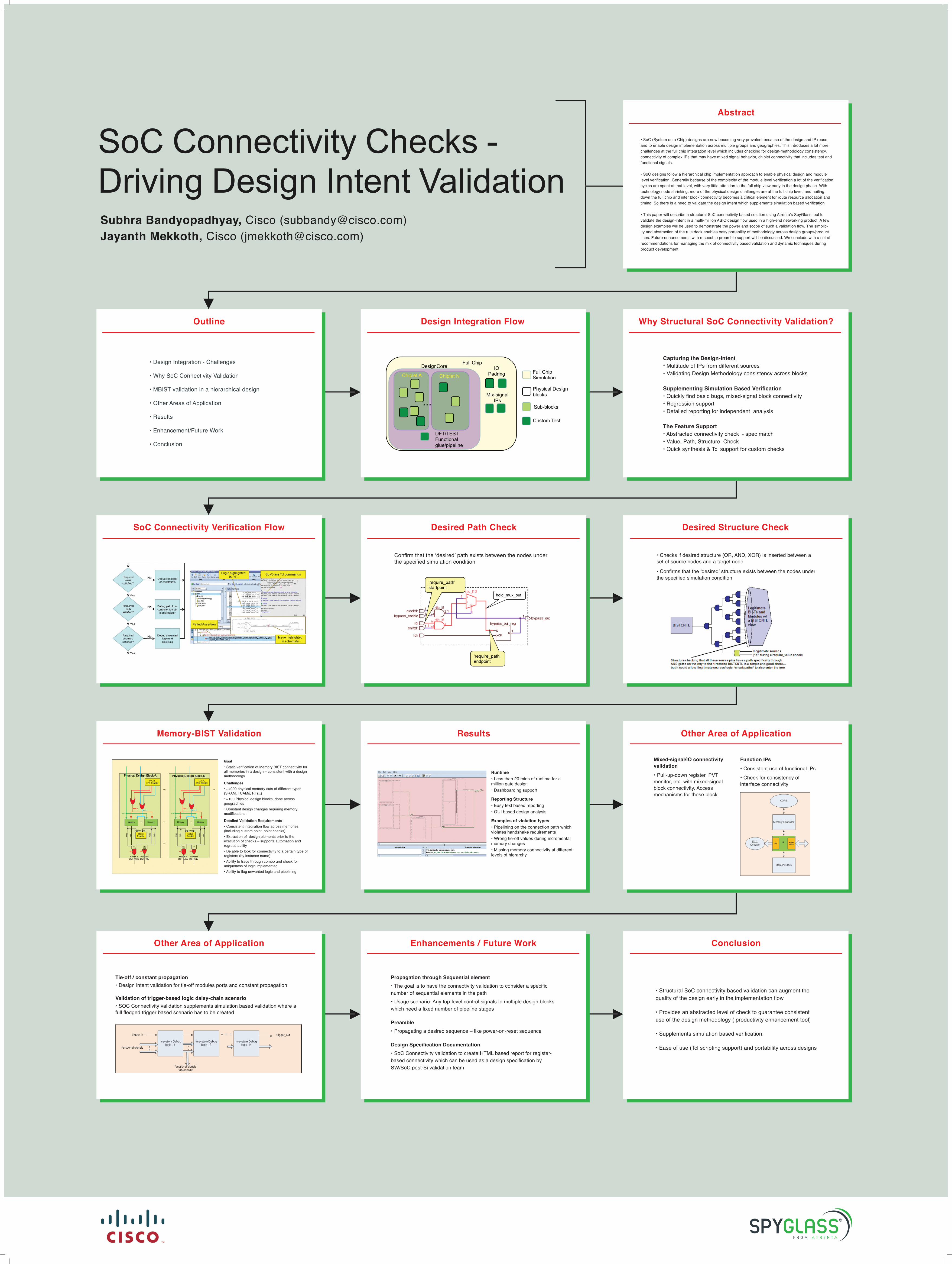
• Checks if desired structure (OR, AND, XOR) is inserted between a set of source nodes and a target node
• Confi rms that the ‘desired’ structure exists between the nodes under the specifi ed simulation condition
• Design Integration - Challenges
• Why SoC Connectivity Validation
• MBIST validation in a hierarchical design
• Other Areas of Application
• Results
• Enhancement/Future Work
• Conclusion
Confi rm that the ‘desired’ path exists between the nodes under the specifi ed simulation condition
Tie-off / constant propagation• Design intent validation for tie-off modules ports and constant propagation
Validation of trigger-based logic daisy-chain scenario• SOC Connectivity validation supplements simulation based validation where a full fl edged trigger based scenario has to be created
Propagation through Sequential element• The goal is to have the connectivity validation to consider a specifi c number of sequential elements in the path• Usage scenario: Any top-level control signals to multiple design blocks which need a fi xed number of pipeline stages
Preamble• Propagating a desired sequence – like power-on-reset sequence
Design Specifi cation Documentation• SoC Connectivity validation to create HTML based report for register-based connectivity which can be used as a design specifi cation by SW/SoC post-Si validation team
• Structural SoC connectivity based validation can augment the quality of the design early in the implementation fl ow
• Provides an abstracted level of check to guarantee consistent use of the design methodology ( productivity enhancement tool)
• Supplements simulation based verifi cation.
• Ease of use (Tcl scripting support) and portability across designs
Mixed-signal/IO connectivity validation• Pull-up-down register, PVT monitor, etc. with mixed-signal block connectivity. Access mechanisms for these block
Function IPs• Consistent use of functional IPs
• Check for consistency of interface connectivity
SoC Connectivity Checks - Driving Design Intent ValidationSubhra Bandyopadhyay, Cisco ([email protected])Jayanth Mekkoth, Cisco ([email protected])
Outline Design Integration Flow
Desired Path CheckSoC Connectivity Verification Flow
Memory-BIST Validation
Other Area of Application Enhancements / Future Work Conclusion
Results Other Area of Application
Desired Structure Check
Why Structural SoC Connectivity Validation?
Abstract