Embed Size (px)
Citation preview

ABSTRACT
Title of Document: LINEARIZED OPTICALLY PHASE-MODULATED FIBER OPTIC LINKS FOR MICROWAVE SIGNAL TRANSPORT
Author: Bryan Michael HaasDoctor of Philosophy2009
Directed By: Professor Thomas E. MurphyDepartment of Electrical and Computer Engineering
Several novel phase-modulated fiber optic links for analog or microwave signal
transport up to at least 20 GHz frequency are theoretically developed and
experimentally demonstrated. Each link uses a linearization technique exploiting the
Lithium Niobate modulator's electro-optic anisotropy between orthogonal
crystallographic axes that has not previously been applied to phase-modulated links.
This technique and its variants suppress the dominant third-order distortion product to
extend the sub-octave spur-free dynamic range of the systems, and does so passively
using the modulator instead of with processing at the receiver. Two of the links
incorporate frequency downconversion, with one of them employing a new method to
spectrally filter the local oscillator and signal sidebands together. This both down-
converts the signal to an appropriate intermediate frequency and causes the phase
modulation to appear as intensity modulation for photodetection with a low-speed
detector. This technique does not require a separate optical oscillator source and can
be implemented with commercial hardware.

LINEARIZED OPTICALLY PHASE-MODULATED FIBER OPTIC LINKS FOR MICROWAVE SIGNAL TRANSPORT
By
Bryan Michael Haas
Dissertation submitted to the Faculty of the Graduate School of the University of Maryland, College Park, in partial fulfillment
of the requirements for the degree ofDoctor of Philosophy
2009
Advisory Committee:Professor Thomas E. Murphy, ChairProfessor Mario DagenaisProfessor Christopher C. DavisProfessor Rajarshi Roy, Dean's RepresentativeDr. Timothy Horton

© Copyright byBryan Michael Haas
2009

Preface
He said that there was only one good, namely, knowledge; and only one evil, namely,
ignorance.
–Diogenes Laërtius, Socrates
This has been a rather unconventional journey. I count myself among the extremely
fortunate few who have had the opportunity to complete a Doctoral Dissertation in a
context so far removed from the traditional graduate school track. It is very rare to
find oneself in a “place” that allows one to simultaneously raise a family, support
them in a reasonable manner, serve the Nation, and complete a Doctorate. A lot of
determination, with some good fortune and not a little support and patience by those
around me, coalesced to grant me the chance to satisfy a what in the end is largely a
selfish desire: to earn this degree and contribute to the body of human knowledge in a
tangible way. I am grateful for all the opportunities afforded me, for the support of
everyone around me who helped expose them, and for the self-confidence and
capability I somehow acquired through life to keep stepping off the ledge and grasp at
those opportunities, even when I repeatedly missed and fell.
ii

Dedication
To my wife, Celina, and to my children, Christopher and Emma, for their unending
support and patience while I was in school... again. Guys, I'm done, for now.
iii

Acknowledgements
I thank my advisor, Professor Tom Murphy, for his support and continuous tutelage
during this process. Tom's original idea for this project took root and continues to
grow in many ways and places. I also thank the members of the Defense Committee
for their time and feedback while writing this dissertation.
This work could not have been completed without the indulgences of, and
funding from, the leadership at the Laboratory for Physical Sciences, specifically: Mr.
William Klomparens, Dr. Barry Barker, and Dr. Ken Ritter. I also thank Dr. Tim
Horton, Dr. Paul Petruzzi, Dr. Mark Plett, and Dr. Chris Richardson of LPS for their
technical assistance and innumerable discussions about various parts of my work.
This journey would not have continued to this particular conclusion without
Dr. Norm Moulton's recognition that I was “looking for a home” and Ms. Bernadette
Preston's concurrence to bring me onboard LPS back in 2004.
I also thank, for their technical assistance, advice, and collaboration on certain
experiments, Dr. Jason McKinney, Dr. Vince Urick, and Dr. Keith Williams of the
Naval Research Laboratory, and Dr. Ron Esman and Dr. Steve Pappert of DARPA.
Reaching further into my past, there are several people who provided critical
motivation at just the right points in my life. I thank Dr. Jenny Heimberg, for her
“push” at Corvis and afterwards, Professor Steven Montgomery, for getting me
excited about optics while I was a Midshipman, Mr. Dennis Kedjierski, who gave me
the tools in 11th grade physics to ask the right question and then answer it from first
principles, and finally, Mrs. Blair, who in third grade incubated my desire for learning
such that it achieved a critical mass and could not later be suppressed.
iv

Finally, I would be remiss in not saving my greatest thanks for my parents,
Richard and Cheryl Haas. They very patiently instilled in me that it is good to always
learn more. My father, particularly, deserves thanks for making sure I kept working
on my math homework, despite my protests, until it was correct. I think I got it right
this time.
v

Table of ContentsPreface ........................................................................................................................... ii
Dedication ..................................................................................................................... iii
Acknowledgements ....................................................................................................... iv
1 Introduction ................................................................................................................. 1
1.1 Statement of engineering problem ....................................................................... 3
1.2 Overview of the work .......................................................................................... 4
2 Microwave photonics .................................................................................................. 6
2.1 Limitations of RoF links ...................................................................................... 7
2.2 Current uses for RoF links ................................................................................... 8
2.2.1 Cable television ............................................................................................. 9
2.2.2 Military ....................................................................................................... 13
2.3 Noise and spur-free dynamic range ................................................................... 14
2.3.1 Noise in RoF systems .................................................................................. 14
2.3.2 Defining SFDR ........................................................................................... 20
2.4 Typical antenna remoting transmitter technologies ........................................... 24
2.4.1 Direct modulation ....................................................................................... 24
2.4.2 Mach Zehnder modulators ......................................................................... 25
2.4.3 Electro-Absorption modulators ................................................................... 32
2.4.4 Y-Branch directional coupler modulators ................................................... 32
2.5 Phase modulation ............................................................................................... 32
2.5.1 DSP assisted linearization ........................................................................... 35
vi

2.5.2 Linearized detector ...................................................................................... 35
3 Linearized optical phase modulation by polarization combining ............................. 36
3.1 Third-order IMD suppression: ........................................................................... 36
3.1.1 Theory ......................................................................................................... 38
3.1.2 Experimental setup and results ................................................................... 43
3.2 Second-order / harmonic suppression: ............................................................... 48
3.2.1 Harmonic suppression with a single phase modulator ................................ 48
3.2.2 Experimental results .................................................................................... 49
4 Dual-wavelength linearized phase modulated link .................................................. 52
4.1 Transition from the previous method ................................................................. 52
4.2 Theory ................................................................................................................ 53
4.3 Beyond fifth-order limited operation and linearization tolerances .................... 64
4.4 Experiment ......................................................................................................... 66
4.5 Results ................................................................................................................ 69
4.6 Conclusions ........................................................................................................ 73
5 Dual-wavelength link with downconversion ............................................................ 74
5.1 Original dual-wavelength scheme ...................................................................... 74
5.1.1 Theoretical analysis .................................................................................... 74
5.1.2 Experimental setup ...................................................................................... 78
5.1.3 Results and lessons learned ......................................................................... 80
6 Alternate method for a linearized phase-modulated fiber optic link with
downconversion, for K-band microwave signals ......................................................... 85
6.1 Concept .............................................................................................................. 87
vii

6.2 Nonlinearized (TM-only) link characteristics .................................................... 89
6.2.1 Optimizing the signal .................................................................................. 94
6.2.2 Link metrics: gain and conversion loss ....................................................... 95
6.2.3 Link metrics: noise ...................................................................................... 98
6.2.4 Optimizing noise figure .............................................................................. 99
6.2.5 Link metrics: filtering ............................................................................... 101
6.2.6 Link metrics: SFDR .................................................................................. 103
6.3 Linearized Link Characteristics ....................................................................... 103
6.4 Experiment ....................................................................................................... 107
6.5 Results and discussion ..................................................................................... 112
7 Future work and extensions .................................................................................... 116
7.1 Modulator efficiency ........................................................................................ 116
7.2 Filter performance ............................................................................................ 117
7.3 Shot-noise limited sources ............................................................................... 117
7.4 Dual-sideband recovery ................................................................................... 119
7.5 Ultimate link goals ........................................................................................... 121
7.6 Digital signal performance testing ................................................................... 122
8 Conclusion .............................................................................................................. 125
Appendix A: Measuring a phase modulator's Vπ ...................................................... 127
Glossary ..................................................................................................................... 131
Publications and presentations ................................................................................... 134
Bibliography .............................................................................................................. 135
viii

List of TablesTABLE 4.1: Calculated and measured link performance............................................72
TABLE 6.1: Calculated and measured link performance..........................................114
TABLE 7.1: Shot-noise limited link budget..............................................................118
ix

List of FiguresNotional antenna remoting scenarios.............................................................................4
Attenuation of a high-quality coaxial cable...................................................................7
Typical CATV HFC network.......................................................................................11
PIN receiver noises versus receiver photocurrent........................................................18
Balanced differential photodetection...........................................................................20
Dynamic Range............................................................................................................21
Geometrical representation to determine SFDR and NF.............................................23
Canonical z-cut Mach-Zehnder modulator..................................................................26
Phasor diagram representation of a MZM...................................................................26
Sinusoidal output from a MZM...................................................................................28
Two MZMs set up in series to linearize a RF signal....................................................29
Linearization by partial cancellation of the signal.......................................................29
Linearization scheme using a single phase modulator.................................................37
Heterodyne receiver system.........................................................................................37
Experimental setup.......................................................................................................44
Spectrum Analyzer traces for two-tone IMD test........................................................45
Received versus input RF power.................................................................................47
Experimental setup for second-order suppression.......................................................49
Fundamental and second harmonic power...................................................................51
SFDR comparison........................................................................................................51
Dual-wavelength linearized phase-modualted link......................................................55
Asymmetrical Mach-Zehnder interferometric filter....................................................58
x

Tone and IMD powers versus m2 ................................................................................65
Dynamic range variation with small deviations...........................................................66
Measured and calculated signal and IMD powers.......................................................70
Schematic of the proposed research link.....................................................................79
Unstable IF phasing between wavelengths..................................................................81
Modified design...........................................................................................................83
Improved phase stability..............................................................................................84
Dual-wavelength linearized down-converting phase-modulated link.........................88
Spectrum of signal, LO, their harmonics, and intermodulation products....................91
Normalized received RF power...................................................................................94
Relationship of system noise figure to LO modulation depth...................................101
19.7 GHz LO tone, phase modulated onto a 1549.62nm carrier...............................109
Tone near 20GHz modulated onto a 1549.62nm carrier with no filtering in place....111
Same tone and carrier, with the FBG in place............................................................111
Measured and predicted down-converted signal and IMD powers............................113
Proposed modification to accommodate dual-sideband recovery.............................121
Plots of calculated RF gain,SFDR, and noise figure.................................................124
xi

1 Introduction
Fiber optic links offer a number of advantages over coaxial transmission lines for
transporting microwave signals. Advantages include enormously larger available
bandwidth, negligible signal attenuation within the fiber, generally smaller size,
weight, and power consumption, immunity to electromagnetic interference in the
transmission media owing to its dielectric nature, and perfect electrical isolation
between the input and output ports. These advantages generally increase as the
microwave frequency and/or the transmission distance increases; higher frequency
results in higher signal attenuation and greater link complexity for conductive
transmission whereas the very low attenuation in fiber allows a fiber link to send a
signal much further. As a result, fiber optic links are often used to supplement or
replace coaxial cable transmission when any combination of the above conditions are
encountered. The use of fiber links to transport such signals is referred to as “Analog
Photonics,” “Microwave Photonics” or “Radio Over Fiber (RoF).”
The act of modulating an optical carrier with a microwave signal and then
demodulating it at the receiver, however, can cause several orders of magnitude worth
of signal attenuation and introduce distortion that is generally not present with coaxial
lines. A candidate fiber optic link, then, needs to have sufficiently low signal loss
(conversely, low Noise Figure, NF) and large enough dynamic range such that its
limitations do not decrease the larger system's performance. There is a large body of
research and commercially available work [1-3] aimed at increasing the dynamic
range and lowering the signal loss (and noise figure). Many of these techniques
introduce significant complexity at the modulator; this is undesirable for the “antenna
1

remoting” scenario which will be detailed.
The fiber optic links presented in this work reduce the remote-end complexity
by using a simpler modulator, increase linearity by suppressing the dominant
distortion order, and progressively strive to make the receiver as simple as possible.
Although the use of optical phase modulation for RoF links is not novel, the
linearization techniques for a phase modulated link as demonstrated here are new.
Where possible, passive components are used to simplify the architecture and make
the link as maintenance-free as possible while ensuring high dynamic range
performance.
A further complication when dealing with high-frequency microwave signals
in the several-GHz range is the need to down-convert the received signal to an
intermediate frequency (IF), usually in the VHF band, more appropriate for
digitization and follow-on signal processing. As in coaxial transmission systems,
most fiber links require an electronic mixer to perform this function, which introduces
further conversion loss and nonlinearities. Complexity at the remote
transmitter/modulator is further increased if the downconversion is performed prior to
the optical link, since the mixer, local oscillator (LO), and associated power and
controls are now required at the remote site. Two of the three different links
presented in this thesis incorporate frequency downconversion with no additional
penalty beyond that incurred by the link itself. The final link design uses a
downconversion technique different form traditional heterodyne detection that has not
been applied to phase-modulated links to date, while also providing a means for direct
detection of the phase-modulated signal.
2
1.1 Statement of engineering problem
The link architectures developed here are for a generic antenna remoting / RoF
scenario, as notionally illustrated in Fig. 1.1. For antenna remoting, a single or
number of RF signals of unknown strength and frequency, possibly in the presence of
large interfering signals and other noise, are fed from an exposed antenna or sensor
that often needs to be very simple, low-cost, and expendable in some fashion. The
receive end of this link, however, is situated some distance away in a more secure
location with more relaxed Size, Weight, and Power (SWAP) considerations and
perhaps trained personnel to operate the receiver. Thus, complexity in the link should
be contained within the receiver and the remote end should be as small, simple, and
inexpensive as possible.
Most optical modulation techniques for RoF require some electronics and
power at the remote transmitting end of the link, even if simply for biasing a
modulator. Even more complexity is needed to achieve low noise figure (e.g. use of a
preamplifier) or high dynamic range (e.g. multiple bias loops, electronic pre-
distorters, or additional modulators) A phase modulated link, however, requires no
biasing or other local electronics at the transmitter, and uses a very simple modulator.
As with nearly all fiber optic links, the exceptionally low loss of optical fiber makes it
possible to deliver the optical carrier to the remote transmitter on an unmodulated
uplink fiber originating from the same physical location as the receiver, eliminating
the need for powered optoelectronic components at the remote transmitter. Thus, a
phase-modulated link most closely matches the SWAP requirements for many
remoting applications by minimizing complexity at the remote transmitter. The
3

challenge is to develop a phase-modulated link with significantly improved
performance over traditional links in order to justify the more complex receiver. It
must have as much dynamic range as possible with as little added noise as possible,
while minimizing the exposed footprint and power consumption.
1.2 Overview of the work
This work is divided as follows: Chapter 2 is an introduction to microwave signal
relay over fiber optics, with a survey of different techniques used and the current state
4
Figure 1.1: Notional antenna remoting scenarios. (a) Coaxial-based transmission requiring bulky, heavy cable and periodic amplifiers and equalizers that each require external power. (b) Fiber-based link requiring minimal power at the antenna, and no in-line complexity for arbitrarily long distances. No external power at the antenna is required for sufficiently efficient modulators.

of the art. Chapter 3 presents the results from the initial proof-of-concept experiments
on a linearized phase-modulated system. Chapter 4 details results from a related
technique that removed complexity at the modulator. Chapter 5 describes the initial
attempt to combine the simplified transmitter with heterodyne downconversion and
why it was not successful. Chapter six presents an improved technique that uses the
same transmitter with a very different optical single-sideband receiver to down-
convert and detect the signal. Finally, Chapter 7 reviews planned engineering
improvements to the design from Chapter six, striving to achieve the maximum
possible dynamic range and noise figure using state of the art components.
5

2 Microwave photonics
There are many situations where it is necessary to relay an RF or microwave signal
over a distance or through an environment that is not amenable to traditional
conductive transmission lines (e.g. coaxial cable). This may be because attenuation
of the signal within the coax would require an amplifier/equalizer chain that cannot
be supported due to power or space constraints, or that would add too much noise
and/or distortion to the desired signal. The signal path may also pass through a
hostile electromagnetic environment where crosstalk or EMI will degrade the signal
despite significant shielding (further adding to size and mass of the system).
Fiber optic relay of the radio/microwave signal is an attractive option in
situations such as these. Unlike coaxial cable, optical fiber has essentially flat
attenuation throughout the entire spectrum used for communications which allows
very broadband operation with a single "pipe." The useable spectrum within just the
C-band for fiber communications, centered near 1550nm, is 4.4THz, with typical
attenuation in standard fiber of 0.25dB/km [4], whereas high-quality coaxial cable
such as LMR-600 has an attenuation of 145dB/Km at only 2.4GHz [5]. Even non-
optimized optical relays can provide less RF-to-RF signal attenuation when compared
to an unamplified coax link for distances as short as 50 meters [6], with the threshold
distance getting shorter as the frequency of interest increases. Since the optical signal
propagates through a dielectric fiber as opposed to conducting coaxial cable, EMI and
intrusion of unwanted signals or leakage outwards of signals is completely
eliminated.
6

2.1 Limitations of RoF links
The act of modulating and/or demodulating an optical carrier is a nonlinear process
which creates distortion that would not be present had the signal been simply
transmitted from the antenna (or other sensor) over coaxial cable (assuming no
nonlinear elements, such as amplifiers, are present in the coaxial link), to the radio
receiver. In particular, the dominant distortion product that falls within a sub-octave
7
Figure 2.1: Calculated attenuation of a high-quality coaxial cable, LMR-600, in dB per kilometer. The attenuation of SMF-28 fiber using a 1550nm optical carrier is 0.25 dB/km, with 4.4 THz of available bandwidth in the 1550 transmission window alone.

signal bandwidth is the third-order intermodulation distortion (IMD). This IMD
occurs when any two frequencies υ1 and υ2 pass through a nonlinear element,
redistributing a portion of their energies into new spectral products at (2υ1-υ2) and
(2υ2-υ1). Although the second-order harmonic and sum/difference products are larger
than IMD, they can be filtered out if the signal itself occupies less than an octave of
instantaneous bandwidth, and in certain cases they may not exist at all (e.g.
quadrature-biased Mach-Zehnder intensity modulation).
Compounding this distortion handicap is the low electro-optic efficiency of
materials commonly used in optical modulators. This prevents efficient modulation
of the original microwave signal onto the optical carrier, causing very poor noise
figures that make it difficult to receive low-power signals at the receiver. Legacy
technologies incur an "E-O-E NF penalty" of ~30dB, given typically several volt
switching voltages and ~milliwatt detector power-handling capabilities. The
contributing factors to optical link noise and noise figure are described in section
2.3.1.
2.2 Current uses for RoF links
Many already appreciate that optical transmission of microwave signals is
competitive with, or superior to, coaxial transmission when link lengths are very long
[6-8]. Applications that require complete electrical isolation between the transmit and
receive end of a link also take advantage of optical relay. The cable television
(CATV) industry is a prominent example of the very widespread deployment of RF-
over-fiber links to cover the long spans between central offices and the edge of their
customer networks, stretching from several to several hundred kilometers.
8

Until very recently, however, there has been an assumption that the noise,
distortion, and loss imparted by optical modulation and detection make fiber a niche
solution, inappropriate for most applications. This assumption has arisen from the
empirical performance of previous and current links, for the reasons stated above. A
system that is limited to ~100dB of dynamic range, with a Noise Figure above 30dB,
and RF-to-RF loss of 20dB is simply unacceptable to many in the industry who would
like to view RoF as a drop-in replacement for passive RF cables. Historically,
improvements over these metrics were hard-fought and incremental, and often
required the use of electronic preamplifiers and/or pre-distortion to improve
performance. Although these systems work and are in widespread use today (see
CATV, below), their hybrid use of optical and electronic technologies adds significant
complexity to the system which is tolerated only because of the economy of scale
uniquely found in broadcast transmission systems.
2.2.1 Cable television
As CATV companies merged and expanded through the 1990s, the smaller, local
networks expanded both in the number of analog television channels offered, and in
their geographic reach. In the 1980s, a CATV provider would typically offer the local
broadcast channels (15-20 channels between VHF and UHF bands in a large market),
two or three premium movie channels, and perhaps a dozen or so other channels, for a
total of maybe three dozen channels, using the frequencies between ~55-300MHz.
By the 1990s this had expanded to nearly 100 analog channels occupying the
spectrum between ~55-800MHz. By the 1990s, the increased hardware, and therefore
higher cost, required to provide this expanded channel lineup often dictated that a
9

single central office serve a region that, in the 1980s, would have been served by
several offices or even different companies. From an engineering standpoint, a single
transmission cable now contained many more individual channels and had to cover
far more distance. This required more amplifiers, exacerbating distortion and noise
problems in addition to the increased composite distortion caused from multiple
channels interacting with nonlinear components. Until the very late 1990s, CATV
signals were fully analog, with no digital services available.
Even with digital signals completely replacing the analog transmissions,
composite distortions caused by the many microwave carrier channels have been
shown to have an adverse effect on bit-error rate, degrading service quality [9-11].
The bit-error rate of a digital transmission, CATV or otherwise, is sensitive to the
signal-to-noise level, and distortion products appear as transient noise. Vector-
modulated signals are further affected by the presence of distortion that causes
changes to the signal amplitude and phase relationships which are critical for proper
reception of the signals[12-15].
The CATV challenge can be summarized as follows: A central office needs to
transmit a single powerful, very "clean," and highly multiplexed set of regularly-
spaced analog signals over a long distance, splitting the signal many times to reach a
large distributed set of inexpensive and effectively disposable receivers (the customer
set-top boxes). An upper limit to the amount of noise and distortion that can be
tolerated on an analog signal is that which still ensures a viewable picture at all
endpoints [16-19]. The digital version of this is ensuring that a worst-case BER is not
encountered. Comparing this to the antenna remoting problem, it is apparent that the
10

CATV problem is almost the inverse. For antenna remoting, one is wiling to accept a
complex receiver in order to simplify or shrink the transmitter. Despite this, several
pieces from the CATV industry can be leveraged to good effect for antenna remoting,
as shall be seen.
The CATV solution, illustrated in Fig. 2.2 [20], was to use fiber optics to carry
the signal from the central office hub to each neighborhood in the network. This
became known as a "Hybrid Fiber-Coax" plant (HFC). Thus, the longest portion of
the network was traversed with a minimum of "in-line" signal loss and complexity,
i.e. few amplifiers or pieces of hardware had to be placed along this part of the
network. A large electronic preamplifier determined the noise floor of this section of
the network to overcome the E-O-E noise penalty, and the signals were
simultaneously modulated onto the optical carrier either with direct modulation of a
laser or by any of a number of external modulation techniques. For particularly long
links, a single or small number of Erbium-Doped Fiber Amplifiers (EDFA) could
11
Figure 2.2: Typical CATV HFC network

effectively maintain signal levels to the local neighborhood. Once the neighborhood
was reached, the optical signal was demodulated back into the electric domain and
traditional RF electronics were used to filter, amplify, and distribute the signal over
the fairly short distances within a neighborhood.
With the noise floor largely set by the front-end electronics and output
received power determined by the local electronics, there remained the challenge of
ensuring that the E-O-E conversions did not unacceptably distort the signal. A
significant amount of academic and industrial research went into improving RF
linearity performance in fiber systems that enabled this very successful application.
Much of the literature about linearized optical links from the 1980s and early 1990s
specifically points to CATV as the motivation for the research [21-29]. The dominant
goal frequently was to ensure that Composite Triple Beat (CTB) and Composite
Second-Order (CSO) distortion were kept to acceptable levels. "Acceptable Levels"
were industry-defined as a cutoff level that qualitatively made a television channel
"unwatchable" to the common customer [30,16-19]. (CTB and CSO are the net third-
and second-order distortion products generated by all of the individual signals
multiplexed together.)
There arose two primary techniques of maintaining linearity that continue to
compete in the marketplace: electronic pre-distortion and optical linearization. Each
was adapted from similar methods used for long distance/high power microwave and
telephony systems [31]. Both methods add significant complexity at the transmission
end of the system; this is acceptable for CATV applications since the transmission
occurs at a secure central office, with few size/weight/power (SWAP) constraints, and
12

with easy access to trained technical personnel to operate and maintain the
equipment. Containing the system complexity within the central office is important
for CATV, since the receiver sitting on top of a customer's television cannot be overly
complex, expensive, or require expertise to operate.
The predistortion technique is best exemplified by Optium's (now Finisar)
MDS-00022 system which is the heart of the distribution system for Scientific
Atlanta's (now Cisco's) cable television (CATV) offerings. Optical linearization was
adopted by Motorola in the GX2 platform, and employs a dual MZM design to cancel
distortion created by one modulator by setting the second in opposition, as will be
detailed later.
The work done to develop highly linear optical links for regularly spaced
multiplexed television signals is directly applicable in general to linearizing for any
application, since CTB/CSO are simply the summation of all individual distortion
products. Although the CATV network design is not generally of much use for
antenna remoting, the device-scale linearization techniques are. In the modern
environment where economics drives much of the direction of research, it is fair to
say that CATV has been the dominant application driving RoF for a long time, and
the lessons learned and technologies developed are not easily ignored. Whatever can
be salvaged and adapted for other uses, should.
2.2.2 Military
Perhaps the most demanding environment for an antenna remoting link is military
application. In many tactical scenarios, the antenna is particularly exposed, and if the
receiver or operating personnel are close by they too become exposed. However,
13

these systems need to be highly mobile, and often man-portable. The remote antenna
and anything connected to it should ideally be expendable; the ability to "cut and
run" or be destroyed without losing significant hardware is important. SWAP
requirements are therefore very strict, and carrying a spool of heavy coax to remove
the receiver/operators from the antenna is often not a viable option.
Another common military application is transporting a signal into or out of a
secured environment, where no signal leakage can be accepted. Fiber provides
complete electrical isolation, with no fear of unintentional transmission of protected
communications from the fiber media itself. Similarly, a single fiber is able to carry
many radio signals with extremely high isolation using WDM techniques, allowing a
single fiber penetration through the bulkhead to carry an entire communications load
into or out of a space.
Unfortunately, the noise and distortion of a fiber relay has prevented
widespread use of fiber optics for tactical antenna remoting. Several companies
market RoF links specifically designed for tactical military use [1,2], but all require
preamplification in order to achieve acceptably low-NF performance, and are limited
to <110 dB SFDR.
2.3 Noise and spur-free dynamic range
2.3.1 Noise in RoF systems
Before any discussion of dynamic range can begin, one must understand the
noise present in an optical link, how it affects performance, and how it can sometimes
be manipulated. The most useful metric to understand this is Noise Figure (NF),
14

which is defined as the ratio of the input signal-to-noise ratio to the output signal-to-
noise ratio.
Any detected signal necessarily has noise detected along with it. In antenna
remoting, the microwave signal is detected by the RF antenna and it is this signal plus
its attendant noise that is modulated onto the optical carrier. For a signal originating
with an antenna (an electromagnetic resonator) the input noise power is assumed to
be Nyquist noise [32] which is itself derived from the equipartition theorem with two
degrees of freedom in a one-dimensional resonator. It is given by kBT = -174 dBm /
Hz, where kB is the Boltzmann constant and T is the absolute temperature of the input
resonator, generally given as 290o K. The importance of this input Nyquist, or
thermal, noise cannot be overstated. It is the fundamental limit for system
performance: the ratio between the original signal and its original noise level cannot
be improved. The job of the transmission system (the fiber link in this case) is to do
the least possible damage to this ratio and keep it as close to the original as possible.
This damage is quantified by the noise figure. The noise figure of a system
normalized to a 1 Hz bandwidth is therefore
NF ≡Sout
G system k B T (2.1)
where Sout is the received noise power spectral density at the receiver and Gsystem is the
RF-to-RF gain (loss) of the system. The smaller the noise figure, the less noise has
been added by the system. If the NF of a system is known, the noise floor in any
given bandwidth B is given by
15

Pnoise = NF k B T B . (2.2)
The noise added by the fiber link system has several components; available
receiver thermal noise, detector quantum shot noise, and the optical source noise
itself. The detector is assumed to be non-amplifying (i.e. PIN, as opposed to APD or
PMT detectors). The optical detector can only respond to intensity, so only intensity
noise at the receiver is relevant. Laser sources are not monochromatic and can impart
significant phase noise; this is a problem if there is a phase-to-intensity noise
conversion process and the power of the converted noise has not fallen below that of
the other sources in the desired receiver frequency range [33-37].
If an optical amplifier (Erbium-Doped Fiber Amplifier, or EDFA) is present,
its noise contribution is caused by beating between the signal and the amplified
spontaneous emission (ASE) of the amplifier and the ASE beating with itself, both
generating intensity noise power that is essentially flat for all RF/microwave
frequencies. These are respectively referred to as “signal-spontaneous” and
“spontaneous-spontaneous” beat noises.
The expressions for all these intensity noise sources present in the system are
as follows [38,39]:
16

S 0,input = k BTS 0,output = k B TS 0,laser RIN = ⟨iDC
2 ⟩Zout RIN laser
S 0,shot = 2e ⟨ iDC⟩Z out
S 0,ssp = ⟨iDC2 ⟩Zout 2h NFEDFA
Popt ,i S 0,spsp = ⟨ iDC
2 ⟩Z out 2h NF EDFA
Popt ,i 2
Bo
(2.3)
RINlaser is the measured relative intensity noise per Hz bandwidth of the laser source
(this is not easily modeled and is usually experimentally determined for each laser
used), <iDC> is the DC photocurrent from the average received optical power, e is
the fundamental charge, Zout is the impedance of the receiver, h is Planck's constant, ν
is the optical frequency (approximately 193.1 THz for C-band links), NFEDFA is the
optical noise figure of the optical amplifier, Popt,i is the optical power at the amplifier
input, and BO is the optical bandwidth illuminating the receiver.
Examination of the equations in (2.3) and their representations in Fig. (2.3)
show that as detector current, or equivalently optical power, rises the thermal noise in
the receiver is constant, shot noise power rises linearly with received average optical
power, and the other noises rise quadratically with optical power. The RF signal itself
and therefore its gain is of course also proportional to the optical power
(photocurrent) squared, since power = <i2>Z. This presents clues as to how one
might manipulate a system to keep the noise figure to a minimum. In the absence of
an EDFA, received optical powers that generate photocurrents below approximately 1
mA cause the system noise to be dominated by the receiver's fixed thermal noise. If
the DC photocurrent is larger than ~1 mA, receiver thermal noise is swamped by shot
17

and often laser noise. If the an EDFA is present, its signal-spontaneous beat noise
rapidly dominates, often below even 1 mA. When laser or EDFA noises are larger
than shot noise, the RF noise figure of the system will be fixed at some level and
there is no benefit to further increasing the optical power/ received photocurrent.
Noise figure remains constant because the received RF signal power or RF gain of the
link has the same i2DC dependency as laser and EDFA noise.
If, however, the laser and/or EDFA noise is not present or can be suppressed
below the shot noise level, then a shot-noise limited system will exist, and the NF can
18
Figure 2.3: Plot of PIN receiver noises versus receiver photocurrent. Note the differing slopes between shot (red) and laser (green) and EDFA (blue, magenta) noise powers. The laser is assumed to have -160dBm/Hz RIN and the EDFA has a 5dB NF with -10dBm optical input. With no EDFA and low laser RIN, shot noise will dominate the noise level for currents >1mA.
continue to decrease for reasonable scenarios to a limit of 3 dB [40]. This
suppression is possible with differential balanced detection if the noise presented to
each individual detector is correlated [32,33,41]. Normally this requires the noise to
be added prior to modulation by the RF signal and that complementary RF modulated
outputs are available. In the classical description, each output illuminates an
individual photodiode; the outputs of these diodes are subtracted, either externally in
an electrical hybrid or by series arrangement with a common output, illustrated in Fig.
(2.4). This causes the correlated intensity noise signals to cancel while the anti-
phased RF signal is added. Since there are two detectors receiving the signal, the
signal current is doubled which quadruples the RF signal power (if a hybrid is used,
the improvement is reduced to doubling). The receiver is complicated by the
necessity to exactly match the complementary path lengths in order to achieve this
common-mode intensity noise suppression. With reasonable care and well-
engineered detectors, greater than 30 dB of common-mode suppression can be
achieved. Note that shot and thermal noise cannot be suppressed in this fashion
because they are generated at each detector and are therefore not correlated across
detectors.
19

2.3.2 Defining SFDR
Until this point, only Dynamic Range has been used to roughly describe the
difference between the signal power and the noise or undesired distortion power.
More specifically this thesis deals with the Spur-Free Dynamic Range (SFDR).
SFDR is the difference between the desired signal power and the largest detectable
distortion product (spur) when looking in the frequency domain, as seen in Fig. 2.5.
20
Figure 2.4: Balanced differential photodetection: (a) Two photodiodes arranged differentially, anode-to-cathode, such that the common current output is the “push/pull”subtraction of one from the other. (b) Two individual diodes, their output currents combined in a hybrid; only the Delta output contains the signal and suppressed common-mode noise, albeit with 3 dB lower RF signal.

For sub-octave signals with more than a single frequency component, the dominant
spurious signal is the third-order intermodulation distortion product (IMD) at the
frequencies (2υ1-υ2) and (2υ2-υ1). The dynamic range is maximized when the largest
distortion product power is equal to the the noise power; undetectable at that moment,
but detectable at any higher modulation depth. The dynamic range at this point is the
SFDR. Since distortion products of a given order are proportional to that order power
of the input signal and the signal itself is linearly proportional, the distortion grows
more quickly than the signal. Therefore, the difference between signal and unwanted
distortion can only decrease once the distortion rises above the (fixed) noise floor.
SFDR is usually normalized to a 1Hz bandwidth to simplify scaling the actual
dynamic range for the receiver bandwidth of choice. It must be noted that most real
receivers utilize a bandwidth far greater than 1 Hz.
21
Figure 2.5. Illustration of Dynamic Range, the difference between the signal and largest distortion power. If the noise floor level equals the distortion level then dynamic range is maximized; this is the Spur-Free Dynamic Range (SFDR). Shown here is the spectrum of a two-tone test with the two signals at f1 and f2 and attendant IMD rising to the noise floor.

An examination of Fig. 2.6 shows that the SFDR and NF in dB can be
determined geometrically from a log-log plot of the output RF power versus the input
RF power in each tone; the SFDR3 is 2/3 of the height between the "IP3" point and
the noise floor, or the distance along the noise floor between the signal and IMD
intercepts. As the noise floor rises, the SFDR necessarily decreases and the noise
figure, the difference between the -174 input limit and where the signal rises above
the noise floor, gets larger. More generally, geometrical arguments can be used to
find:
SFDRnth order = [n−1]n IPn−−174NF (2.4)
where IPn is the input power per tone at which the distortion and signal powers would
be equal, if they were extrapolated on the log-log plot. The (-174+NF) term is simply
the noise floor given by (2.2). In particular, this research will be concerned with third
and fifth-order terms of the IMD product, which would have respective slopes of 3
and 5 on the plot.
22

It is important to note that several assumptions must be made when
normalizing SFDR to 1Hz; most directly that the slope of the distortion product line
in Fig. 2.6 remains constant as the noise floor drops with decreased bandwidth and
"reveals" distortion at lower powers. This in turn requires an assumption that the
photodetectors [42-46] and any post-detection equipment (amplifiers, spectrum
analyzers, etc) are completely linear. This is not always the case, and in practice the
23
Figure 2.6: Plot showing the geometrical representation to determine SFDR and NF. Because the signal slope = 1, an isosceles triangle is formed and SFDR (as well as noise figure, NF) can be found vertically or horizontally. Noise figure is the difference between -174dBm input power and the intersection of the linear signal with the noise floor.

distortion product slope can "walk off" of the ideal slope from a combination of these
other distortions not related to the modulator, as the distortion of other components
begins to dominate [47-49]. Therefore it is sometimes preferable to only quote the
actual SFDR achieved in a given receiver bandwidth, preventing accusations of
claiming better performance than what was actually achieved. In actuality, the SFDR
is still usually given in a 1Hz bandwidth, since it is understood by most that some
extrapolation took place because of the difficulty in actually measuring with a 1Hz
receiver. A good practice that will be used is to quote both the normalized SFDR, for
ease of translation, and the bandwidth used to take the measurements, for full
disclosure. From this, an interested party can quickly calculate the actual SFDR that
was measured.
2.4 Typical antenna remoting transmitter technologies
2.4.1 Direct modulation
Within a few years of the invention of the the room-temperature semiconductor laser,
its distortion characteristics were measured and modeled for both intensity and
frequency modulation cases [21,50-58]. Systems were tested that used both intensity
and frequency modulation of the laser's output, at frequencies of up to 12.5GHz.
Fairly inexpensive direct-modulated laser RoF links found some use in CATV and
remoting links through the early 1990s, and can still be purchased for applications up
through several GHz frequencies. Modern high-performance systems generally do
not utilize direct modulation. Although low-frequency modulation at low laser
powers can be very linear, it is difficult to maintain this linear behavior at the high
24

launch powers required for RoF links, and even more difficult to do so at higher
frequencies that may begin to interact with the internal laser dynamics (e.g.
modulating near the relaxation oscillation peak). It is difficult to model this behavior
and adds unwelcome complexity to the system design task.
Another way to modulate light is to impose the radio signal upon the carrier
externally instead of directly modulating the laser drive current or bias voltage. In
modern practice there are two commonly used methods for externally modulating
light: via the Pockels effect, usually but not always within a Lithium Niobate
(LiNbO3) medium, and via the Franz-Keldysh (for bulk semiconductor) or Quantum-
Confined Stark (for quantum well devices) effects in an Electro-Absorption
Modulator (EAM).
2.4.2 Mach Zehnder modulators
The LiNbO3 MZM is often the modulation technology of choice for high-
performance RoF links. Several decades of research and engineering effort have
developed a mature, stable, and robust family of devices that are well understood and
have broad application for digital and analog transmission. The proposed technique
will also use LiNbO3, as a phase modulator, and much of the work done with MZMs
is applicable in one way or another to the proposed technique. A MZM is essentially
a phase modulator that is self-homodyned with its own carrier after undergoing a 90
degree relative phase delay (the bias) shown in Fig.2.7. This shifts the phase-
modulated anti-phased sidebands so their combination results in amplitude
modulation of the carrier, represented in the phasor diagrams in Fig. 2.8.
25

An equivalent and more frequently cited way to envision a MZM is as an
interferometer set such that the reference arm maintains a fixed 90-degree optical
phase bias from the signal arm, resulting in small-signal modulation about the
26
Figure 2.7: Canonical z-cut Mach-Zehnder modulator. The optical carrier is divided equally, with one branch undergoing a 90 degree static phase shift and RF modulation. This branch recombines with the undisturbed carrier at the output.
Figure 2.8: Phasor diagram representation of a MZM. The phase-modulated carrier with sidebands of opposite phase and frequency experiences no net amplitude change because of this. It is combined with an identical optical carrier at the output that has been advanced or retarded 90 degrees relative to the modulated carrier. Their vector sum results in sidebands that now cause the amplitude of the carrier to be modulated, along with some residual phase/frequency modulation that is the characteristic chirp of many z-cut MZMs.

inflection point shown in Fig. 2.9. The second derivative of the transfer function at
this bias is zero, causing second-order nonlinearities to vanish. In normal usage, a
MZM link is biased at quadrature, or the half on/half off state resulting form the 90-
degree phase relationship between the two arms. Maintaining bias at this flat point in
the transfer function eliminates even orders of distortion, leaving the third order as the
dominant distortion products. A MZM-based link is therefore capable of relaying a
multi-octave signal, since there are no second harmonic or sum/difference distortion
products present. The modulation depth is defined as the ratio of applied signal
amplitude voltage to the voltage required to shift the MZM's transmission from
completely off to completely on, also known as “Vπ” because this voltage causes a π
phase shift between the two arms which swings the output from off to on.
27

Much of the research concerned with linearizing, or increasing the SFDR
beyond what would normally be characteristic of a third-order limited link, has
centered on LiNbO3 MZMs [59-66]. Studies of harmonic distortion and IMD
motivated a number of variations on a particular technique: If two modulators, fed by
the same original RF signal, produce modulated optical outputs with different
modulation depths and anti-phased to each other (set on opposite transfer function
slopes) as represented in Fig. 2.10, then the outputs can be combined in some ratio
where the amplitudes of the distortion signal cancel completely, while the other signal
28
Figure 2.9: Sinusoidal output from a MZM illustrating its periodic interferometric nature. Normal usage biases the device at the half-transmission inflection point, presenting a flat transfer function for small modulation excursions about this point.

components only partially cancel. Therefore the final output is an attenuated version
of the original signal, with third-order IMD products largely suppressed, as shown in
Fig. 2.11. This technique is general in that in principle, any single order of distortion
can be suppressed, although the third order is dominant and therefore most useful to
eliminate.
29
Figure 2.11: Representation of linearization by partial cancellation of the signal. Two versions of the signal at differing modulation depths (different xfer function slopes) and the appropriate power ratio are added in opposition, suppressing the distortion and somewhat suppressing the signal as well.
Figure 2.10: Simplified illustration of two MZMs set up in series to linearize an RF signal, which is fed in the proper ratio and phasing to each modulator (from Betts [53]).

The two signals are forced into opposite phasing by positively biasing one
modulator and negatively biasing the other. The differing modulation depth between
two modulators can be achieved in any of several ways: two physically different
modulators can be used in parallel [59] or series [60], or two different wavelengths
(e.g. 1310/1550nm) can be launched into the same modulator [61,62].
Another method of increasing SFDR without actually linearizing is to bias the
MZM very near zero transmission [67-69]. The unmodulated carrier is almost
extinguished, minimizing noise due to the optical link. Noise power is primarily
dependent upon the average received optical power, which is in turn dominated by the
unmodulated optical carrier power. The noise power drops off more rapidly than
signal because the unmodulated carrier power exhibits a different bias dependency
than the signal. Thus SFDR can be extended by lowering the noise floor more quickly
than the signal is attenuated, at a cost of being restricted to sub-octave bandwidths
because of the nonquadrature biasing.
All of these methods are inherently independent of the modulating frequency,
have been shown to be effective at suppressing IMD at RF frequencies ranging from
10MHz through 20GHz, and produce shot-noise limited SFDRs between 125-
135dB/Hz, with the bandwidth dependency being to the 2/3 or 4/5 power depending
whether the link was linearized.
The technique most germane to this work was also one of the first
linearization techniques to be described, by Johnson and Roussell [70,71]. It uses a
single MZM, but exploits the fact that LiNbO3 has unequal electro optic coefficients
30

between the z and x crystallographic axes. Light launched onto each axis is
modulated to different depths. Proper biasing can ensure that outputs are 180 degrees
out of phase, and if the power from each polarization is in the proper ratio, one order
of distortion can be suppressed upon detection.
A MZM can have one or two outputs. If there are two outputs they will be
complementary (180o out of RF phase with one another), and all of the optical power
launched into the device can be recovered with a balanced differential detector. This
provides 6dB more RF gain and a 3dB higher signal-to-noise ratio (SNR) in the shot
noise limit than with a single output. This translates to a 2dB increase in SFDR, for
the same launched optical power. More significantly, the source noise constraints can
be relaxed, since balanced differential detection can be used to suppress common-
mode noise (e.g. laser RIN), making it far easier to ensure a shot-noise limited signal
is received. This has the effect, in practice, of yielding significantly more than 3dB
SNR and 2dB SFDR improvements over single-arm MZM links if the source laser is
not shot-noise limited. The cost for this improved performance is that two separate
output fibers must be run from the modulator to the detector, with the group delay for
each matched across the intended RF bandwidth.
Recent advances in modulator and detector design have greatly reduced the
NF and improved the SFDR of RoF links. Subvolt Vπ in LiNbO3 modulators out to
>10 GHz are possible, and balanced PIN photodiodes can now handle up to 100mA
per diode. Very recent results [72,73] using these state-of-the-art components have
shown single-digit NF and correspondingly high SFDRs using dual-output MZMs
and high-current (20-80mA per diode) integrated balanced detectors.
31

2.4.3 Electro-Absorption modulators
The modulation, noise, and distortion characteristics of EAMs has been
characterized for RoF applications [74,75] They are not commonly found in RoF
links but are included here for completeness. The principal reason they are not used
is the high optical powers normally found in RoF links cannot be safely absorbed by
the EAM, as it creates intensity modulation by absorption instead of scattering or
coupling [40].
2.4.4 Y-Branch directional coupler modulators
Y-branch couplers can be used as intensity modulators by properly biasing closely
spaced adjacent waveguides in an electro-optic material (to vary the degree of
coupling from one arm to the other. The result is similar to that of a Mach-Zehnder,
although it doesn't exhibit a periodic transfer function. Several linearization
techniques have been developed that utilize a Y-branch in conjunction with a MZM
[76-80]. Y-branches are not commonly used as modulators because of the practical
difficulty caused by long interaction lengths needed with very tight waveguide
spacing tolerances to create an efficient modulator.
2.5 Phase modulation
Optical phase modulation has several advantages over intensity modulation, whether
with a MZM or other technology:
- All of the optical power launched into the device (minus the device loss
itself) is output from the device, with a single fiber instead of two separate
outputs that must be path-matched. There is no biasing that intentionally
32

"throws away" power as there is in a single-output MZM.
- Since there is no electrical biasing, the modulator needs no support circuitry
or local optical taps to help maintain bias, making for a smaller physical
footprint at the transmitter.
- Phase modulated light presents a constant average optical power to the fiber
and photodetector, mitigating the onset of certain nonlinear effects such as
self-phase modulation.
- Phase modulation is inherently linear with respect to the input signal voltage
in a Pockels' effect device. The amount of phase retardation of the optical
carrier is directly proportional to the applied voltage supplied by the RF
signal. Related to this, there is no limit to the modulation depth possible with
phase modulation; the modulator transfer function is completely linear, unlike
an intensity modulator that has a maximum modulation stregnth of π radians,
after which the transfer function begins to decrease because of the sinusoidal
shape.
- If heterodyne detection is used, combining with an optical local oscillator
naturally lends itself to balanced detection since there are always sum and
difference outputs from a coupler or beamsplitter/combiner, analogously to the
complementary outputs of a dual-output MZM. This eases requirements on
the source lasers since >20dB of common-mode RIN can be suppressed
through differential detection, enabling shot-noise limited performance
without much difficulty or expense. This also maximizes use of all available
optical power.
33
Phase modulation has not seen very widespread application in optical
communications because of the difficulty in recovering the information contained in
the optical phase. Because phase modulation places the first sidebands 180 degrees
out of phase with one another, direct detection of the signal is not possible since the
information-bearing sidebands cancel when beat with the carrier in the square-law
photodiode. A method to convert the phase-modulated signal into a directly
detectable intensity-modulated signal must be used. In most cases this is an
interferometric or coherent beating process which results in a sinusoidal transfer
function. Thus, although the phase retardation is linearly proportional to the applied
RF voltage, the method required to detect the phase and recover the information
imparts essentially the same distortion to the signal as a signal that was originally
intensity modulated.
Optical heterodyne detection is commonly used to recover the original signal.
The advantage to heterodyne detection is in the fact that it naturally shifts the RF
signal to a different frequency, determined by the frequency offset between the optical
carrier and local oscillator (LO). Furthermore, the use of a powerful LO means high
optical powers are not necessarily required in the link, relaxing the link budget
requirements, since the LO field multiplies with the signal field to effectively increase
the received signal power. As with MZI-assisted detection, phase noise is converted
to intensity noise, and must be accounted for and minimized with low-noise LO
sources [33]. A linearized heterodyne detection technique is also presented in
Chapter 3.
34

2.5.1 DSP assisted linearization
One ongoing research program is to use digital signal processing to linearize a phase-
modulated optical signal. This research is being conducted at the Johns Hopkins
University Applied Physics Laboratory [81-83]. These techniques utilize the in-phase
and quadrature components of the optical signal obtained from a 90-degree optical
hybrid, processing them offline or in real-time to recompute the original optical phase
and thus the signal. Recent extensions to this work have produced linearized and
down-converted signals [84,85] with SFDRs exceeding 130dB/Hz2/3, although signal
recovery was not in real-time.
2.5.2 Linearized detector
A parallel effort at the University of California at Santa Barbara [86] is implementing
a linear receiver by using a phase-lock loop to track the optical phases, instead of
interferometric beating. The detected optical signal is sampled, and a phase-locked
loop correction signal is sent to a phase modulator that modulates a LO in an attempt
to coherently cancel some of the signal upon mixing. This effectively reduces the
modulation depth of the detected signal which lowers the size of distortion.
Knowledge of how much correction was needed allows the detected signal (with no
distortion) to be re-corrected back to the level it would have been had no signal
cancellation occurred. This effort has yielded 125dB/Hz SFDR in the shot-noise
limit, although the system itself is not shot-noise limited, giving a real SFDR of
~110dB/Hz. The current receiver bandwidth of this technique is limited by the speed
of the correction loop currently to approximately 300MHz. Similar feedback loops
driving a LO modulator are also being investigated at Drexel University [87,88].
35

3 Linearized optical phase modulation by polarization combining
The linearization method described here is an adaptation of Johnson and Roussell's
technique, as applied to a phase modulator. This first effort exploited the anisotropic
nature of LiNbO3 to modulated orthogonally polarized optical fields. These two
fields were then combined to eliminate the third-order distortion. Only a single phase
modulator was required, and the received signal was demonstrated to be limited by
fifth-order IMD instead of the larger third-order. Both third [89,90], and later second-
order [91] distortions were separately suppressed, which experimentally verified the
validity of using the different polarization axes within a telecom-grade phase
modulator to linearize the output signal response from a link.
3.1 Third-order IMD suppression:
LiNbO exhibits an electrooptic coefficient along the (TE) axis which is approximately
1/3 of the coefficient on the (TM) axis, the ratio remaining constant over temperature.
[92] A similar anisotropy is seen in electrooptic polymers [93]. This method makes
use of this anisotropy to simultaneously phase modulate two orthogonal polarization
states by different amounts. As shown in Fig. 3.1, if the optical signal entering a
phase modulator is polarized at an angle with respect to the z - axis, it excites a
superposition of TE and TM modes that will be modulated to different depths. In this
way, a single device can simultaneously play the role of two phase modulators
connected in parallel. As described in the following section, when the output signal is
projected onto a fixed polarization axis, it is possible to eliminate the third-order
36

IMD, leading to improved SFDR. The rest of the system is a traditional heterodyne
receiver as shown in Fig. (3.2), using an acousto-optic frequency shifter to create an
optical LO near the signal for detection.
37
Figure 3.1. Linearization scheme using a single phase modulator. The input optical signal is linearly polarized at angle θ and the output polarizer is oriented at angle α, which is chosen to eliminate third-order distortion in the signal.
Figure 3.2: Heterodyne receiver system for detecting and down-converting the linearized phase-modulated signal.

3.1.1 Theory
The idea of using polarization mixing to achieve linearization was originally
proposed and demonstrated in Mach–Zehnder intensity modulators [70,71], but until
now has never been applied to the case of phase modulation. To analyze the
modulator shown in Fig. 3.1, we begin by assuming that the input electrical signal is a
sinusoidal modulation at the microwave frequency Ω
v t = V 0sin t (3.1)
and that the electric field of the input optical signal entering the device can be
represented by
E t = E0 z cosx sine jt (3.2)
where ω is the optical carrier frequency and θ describes the angle of polarization. If
we neglect the birefringence of the device, the optical field of the phase-modulated
signal emerging from the device is given by
E t = E0 z cos e jmsin txsin e j msinte jt (3.3)
where m ≡ πV0/Vπ(z) is the modulation depth for the z -polarized component of the
field and γ is a dimensionless ratio (less than 1) that describes the ratio of the
electrooptic modulation depth in the x direction to that in the z direction, where m
itself is proportional to the input RF signal drive voltage. Ultimately this ratio
38

depends on the Vπ switching voltage for each axis, which depends, among other
things, on the electro-optic tensor element and the index of refraction for the
respective axes. This ratio in LiNbO3 is approximately 1/3,
Phase modulation generates an infinite number of harmonic sidebands, but by
properly choosing the frequency of the local oscillator and the bandwidth of the
heterodyne receiver, one can ensure that the receiver responds only to the first upper
sideband. Applying the Bessel function expansion to (3.3), and neglecting all but the
upper sideband gives
E t = E0[ z cos J 1m x sin J 1m ]e j t . (3.4)
After the microwave signal is modulated onto the two polarizations, the TM
and TE fields are recombined at the output as in Fig. 3.1 with a linear polarizer set at
angle α to the z, or TM, axis. The component of the electric field transmitted by the
polarizer at angle α is then given by
E t = E0[cos cos J 1msinsin J 1m]e j t . (3.5)
The nonlinear components of the modulated signal are revealed by Taylor
expanding the Bessel function J1(m) to third order in m
E t =E0
2 [cos cos m−18
m3sinsinm−183 m3]e j t . (3.6)
From (3.6), one sees that the terms proportional to m3 can be eliminated under the
following condition:
39
coscos3sin sin= 0. (3.7)
Although this equation does not have a unique solution for θ and α, one
reasonable choice is to select the combination that maximizes the component
proportional to m while canceling the components proportional to m3. This yields the
optimal solution
=− =± tan−1−3/2. (3.8)
The preceding analysis is valid for a signal consisting of a single tone. Now
an analysis with two tones will be presented to show that the third-order
intermodulation products at (2Ω1-Ω2) and (2Ω2-Ω1) can be suppressed with the same
solution according to (3.7). Including higher order sidebands in the analysis enables
one to find conditions that suppress any other single distortion order.
To show how the IMD products are generated in phase modulation, (3.3) is
adapted and two sinusoids of different frequency and possibly different modulation
depths are placed in the phase argument modulating the carrier:
E t = E0 z cos e jm1 sin 1m2 sin 2 tx sine j m1 sin1 m2 sin2 te j t . (3.9)
This can be rewritten as
Eout t =E0 e jt ∑p=−∞
∞
∑n=−∞
∞
J pm1J nm2ej p1n2 t (3.10)
by using the Bessel relation
40

e jk sinx = ∑n=−∞
∞
J n k ejnx . (3.11)
With the use of
J−nk = −1n J nk (3.12)
the field components generated by the interaction of the first two upper and lower
sidebands that fall near the original signal frequencies after the output polarizer are
E t = coscosE0 J 1m1 J 0m2ej 1 t e j t
cos cos E0 J 0m1 J 1 m2ej 2 t e jt
−cos cos E0 J 1m1 J 2m2ej 22−1 t e j t
−cos cos E0 J 2m1 J 1m2ej 21−2 t e j t
sinsin E0 J 1m1 J 0 m2ej 1 t e jt
sinsin E0 J 0m1 J 1m2ej 2 t e jt
−sinsin−E0 J 1m1 J 2 m2ej 22−1 t e j t
−sinsin−E0 J 2m1 J 1 m2ej 21−2 t e j t .
(3.13)
The third-order components of both the original signal frequencies and the IMD
products are seen by Taylor expanding the Bessel terms:
J 0 x= 1− x 2
4...
J 1x = x2−
x3
16...
J 2 x = x2
8−
x4
96...
(3.14)
and keeping the linear and third-order terms to get:
41

E t = z coscosE0m1
2−
m13
16−
m2 m12
8 e j 1 t e j t
z cos cos E0m2
2−
m23
16−
m1m22
8 e j 2 t e j t
−z cos cos E0m1 m22
16 e j 22−1 t e jt
−z cos cos E0m2 m12
16 e j 21−2 t e jt
x sinsin E0 m1
2−m1
3
16−3 m2 m1
2
8 e j 1 t e j t
x sinsin E0 m2
2−m2
3
16−3m1 m2
2
8 e j 2 t e jt
−x sinsin E0 3 m1 m22
16 e j 22−1 t e j t
−x sinsin E0 3 m2 m12
16 e j21−2 t e jt .
(3.15)
If m1 = m2, the math simplifies somewhat; the (2Ω1-Ω2) and (2Ω2-Ω1) terms look
exactly as in (3.6), and the remainder of the solution follows as above. Furthermore,
the third-order portion of Ω1 and Ω2 have the same coefficients and will similarly still
be canceled when the same condition is met. However there is not requirement for m1
to be equal to m2.
Now that the third order has been suppressed, the remaining fifth-order
distortion needs to be checked to determine which product is the largest. In addition
to the residual fifth-order term of the IMD at (2Ω1-Ω2) and (2Ω2-Ω1), there are new
fifth-order intermodulation terms at (3Ω1-2Ω2) and (3Ω2-2Ω1) that can be found when
continuing the above analysis with higher-order terms. These fifth-order products
generally fall within the signal bandwidth as well; their amplitude varies as
J2(m)J3(m) which expands to m5/128, significantly smaller than the 5m5/384
42

amplitude of the fifth-order residual (2Ω1-Ω2) and (2Ω2-Ω1) IMD products. Therefore
the residual IMD products are still larger than the pure fifth-order terms.
As with most linearization schemes, the enhanced linearity comes at the
expense of reduced efficiency. When θ and α are chosen according to (3.8), the
transmitted amplitude is reduced by a factor of
[ 1−213 ] (3.16)
compared to what it would be if the input signal were polarized in the TM, or z
direction. This decrease is caused by the opposing transfer functions, which in
addition to canceling the third-order terms, also reduce the linear terms. For the case
of LiNbO3 where γ is approximately 1/3 , the linear signal amplitude is predicted to
decrease by a factor of 2/7, or a power reduction of nearly 11 dB compared to the
TM-polarized case. Optimizing (3.16), one finds that the ideal ratio of γ = 1/ 2 results
in only 9.5 dB power reduction.
3.1.2 Experimental setup and results
Fig. 3.3 depicts the experimental setup used to demonstrate linearized phase
modulation. The electrooptic modulator was a standard Ti-diffused z-cut LiNbO3
waveguide phase modulator, originally designed for digital operation up to 12.5 Gb/s.
At a frequency of 1 GHz, the TM half-wave voltage of the modulator was measured
as 4.25 V as described in Appendix A. The housing was opened and fiber pigtails
removed to expose the crystal facets and enable free-space coupling into and out of
43

the waveguide. Two equal-amplitude sinusoidal tones with frequencies of 979.5 and
980.5 MHz were combined and applied to the electrooptic modulator. Device
birefringence at this frequency was calculated to cause about 12ps differential group
delay or 4.5 degrees of phase difference at the 1 GHz microwave carrier frequency,
with weak temperature dependence.
As shown in Fig. 3.3, the signal and local oscillator were generated from the
same laser source, which ensured phase coherency in the heterodyne detector for
short, stabilized links. The local oscillator was generated by translating the carrier 1
GHz using an acousto-optic frequency shifter, which placed the local oscillator in the
vicinity of the first upper sideband of the modulated signal. When the two-tone
modulated signal and local oscillator were combined in the heterodyne detector, they
produced down-converted electrical tones at the intermediate frequencies of 19.5 and
20.5 MHz.
A linear polarizer and adjustable half-wave plate were inserted at the input of
the modulator to set the input polarization angle θ, while an adjustable linear polarizer
at the output was used to project the modulated output signals onto an axis oriented at
44
Figure 3.3. Experimental setup for demonstrating linearized phase and polarization and heterodyne detection and downconversion.

angle α to the z axis. The output polarization selection could also be accomplished at
the receiver by controlling the polarization state of the local oscillator. The optimum
input and output polarization angles were adjusted to be approximately +/-78o , based
upon (3.8), assuming γ = 1/3. Fine adjustments were made to the polarization angles
while observing the detected output spectrum to locate the settings at which the IMD
was minimized.
Fig. 3.4(a) plots the measured electrical spectrum of the down-converted
output signal when the input signal was linearly polarized along the TM axis of the
waveguide, whereas Fig. 3.4(b) plots the spectrum obtained when the input and
output polarization angles were adjusted for optimal linearity. In the latter case, the
input electrical power was increased by approximately 10 dB in order to maintain the
same detected fundamental output power. Despite the stronger driving voltage, Fig.
3.4(b) clearly shows that the third-order IMD can be suppressed by using the mixed
polarization state.
45
Figure 3.4. Spectrum Analyzer traces for two-tone IMD test for (a) traditional TM input polarization and (b) mixed polarization. For (b), the input RF power was increased by approximately 10dB to maintain the same tone output power. Note that the IMD products are suppressed to the noise level.

Fig. 3.5 plots the measured output tone and IMD power as a function of the
input RF power applied to the modulator. The open squares show the performance
obtained when the input signal was TM-polarized, while the filled circles show the
results obtained by using a mixed polarization state described here. The dashed and
solid lines indicate a theoretical fit to the measured data, based on a complete
calculation of the two-tone spectrum. The calculated results have been adjusted in
power and γ to account for inefficiencies and uncertainties in the experimental setup.
As expected, the TM case exhibits third-order IMD similar to what is routinely seen
in Mach–Zehnder amplitude modulators. For the mixed polarization case, the
intermodulation tones at (2Ω1-Ω2) and (2Ω2-Ω1) increase by 5 dB for every 1 dB
increase in the signal power, which indicates that the third-order distortion has been
eliminated and that linearity is instead limited by fifth-order distortion. Even though
the linear tones have reduced power in the mixed polarization case, the dynamic
range between the tones and IMD is significantly improved for a given input power.
46

47
Figure 3.5. Received versus input RF power for both TM (dashed) and mixed (solid) polarizations, plotted with calculated results. The upper points with slope = 1 are the down-converted tones while the lower points are (down-converted) third- and fifth-order IMD powers, respectively.
3.2 Second-order / harmonic suppression:
This adaptation of the same technique from the previous section shows that it is not
limited to only suppressing the third-order distortion. One disadvantage of phase-
modulated links relative to quadrature-biased MZM links is that the second-order
distortion is not automatically suppressed. This causes sum/difference and harmonic
products to be present if the instantaneous microwave bandwidth of the signal is
greater than a single octave. For a down-converting link this is an unrealistic
scenario, since any down-converted superoctave signal still occupies part of the
original signal bandwidth. However, a heterodyne link can also be used to upconvert
a signal, and it is possible for a superoctave signal at the original (low) frequency to
be upconverted. For this scenario, the following experiment shows it is possible to
ensure that a superoctave signal in a phase-modulated link can still achieve third-
order limited performance matching a MZM link by suppressing the harmonic and
sum/difference products.
3.2.1 Harmonic suppression with a single phase modulator
The polarizer angles needed to suppress the second order can be calculated by
solving the expanded form of a PM signal such that the second-order terms add to
zero. For a single microwave tone (Ω) applied to the optical carrier (ω), the output
from the second polarizer can be described as:
Eout t = E 0[cos cos e jmsintsin sin e jmsin t ]e jt (3.17)
48

where θ and α are the angles represented in Fig. 3.1, m is the modulation depth again
defined as πV0/Vπ(z), and γ is the electro-optic ratio between TE and TM
(approximately 1/3). The exponential terms in (3.17) can be expanded as series of
Bessel functions, which in turn can be Taylor expanded as in the previous section.
This time, setting the 2nd-order terms of the expansion to equal zero and optimizing
the remaining fundamental term, one finds the optimal polarization angles to be:
=− =±tan−1−1. (3.18)
3.2.2 Experimental results
Fig. 3.5 describes the experimental setup used to demonstrate the technique., which
was functionally identical to that used in the earlier experiment. A single tone at
105MHz was used for the signal, and its upconverted second harmonic at 1210MHz
was minimized. Note that results and noise shown here are for "up shifted"
heterodyne detection. The input and output polarizations were adjusted in accordance
with (3.18) and then fine-tuned while observing the output spectrum to determine the
exact settings which minimized the second harmonic product.
49
Figure 3.6. Experimental setup for second-order suppression.

Fig. 3.6 plots the experimentally observed fundamental and harmonic powers
for both "normal" TM modulation and the mixed polarization technique described
here. Despite the signal power penalty caused by the linearization and possibly
polarization-dependent loss in the modulator, the mixed polarization results clearly
show that the second order dependence of the harmonic has been suppressed, and that
it is a fourth-order term that remains.
Fig. 3.7 plots the calculated performance of a MZM link with the same Vπ
and modulated optical power alongside the calculated response of a second-order
suppressed PM link. From this one can see that the (superoctave) SFDR and noise
figure of the mixed-polarization PM link matches that of the MZM link, since the
second order has been suppressed and the third-order is now the limiting distortion
product. Furthermore, the phase-modulated link incorporates frequency upconversion
whereas the MZM link does not, and would require an electrical mixer for this,
incurring further power loss and possibly adding distortion.
50
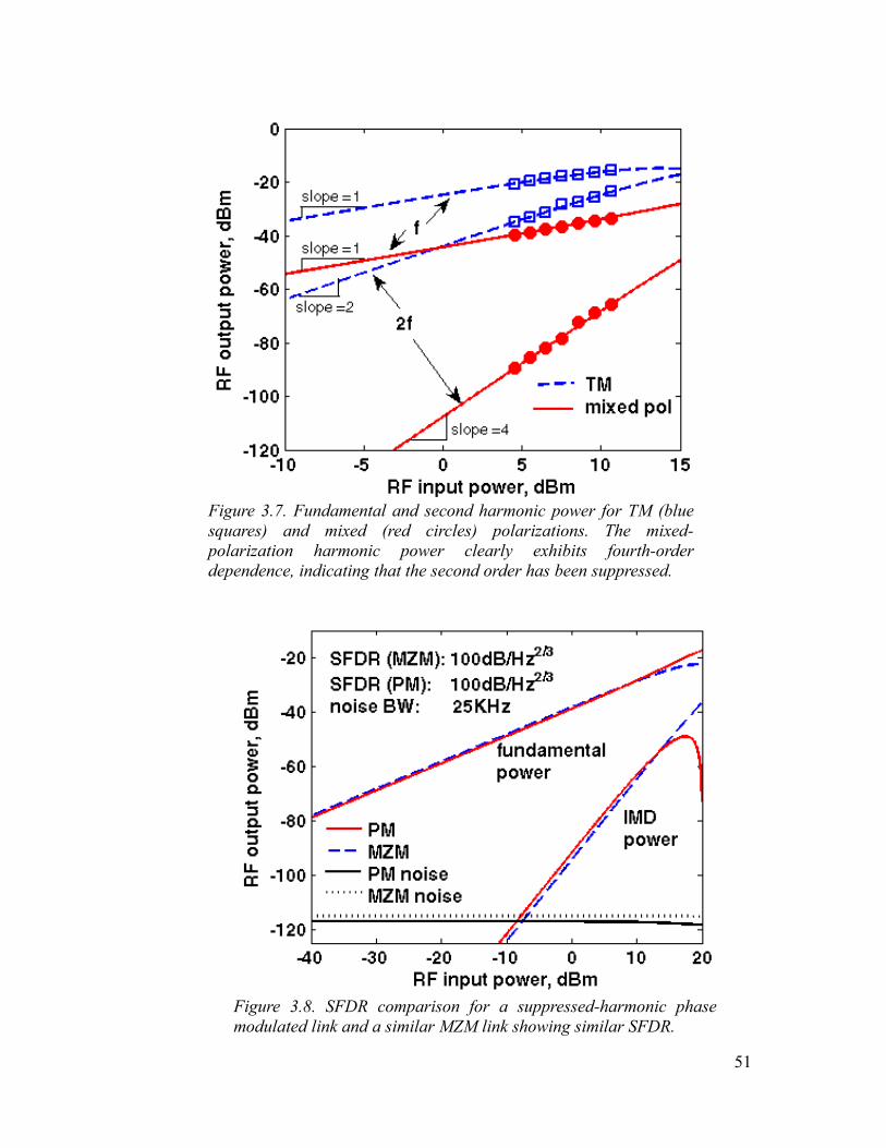
51
Figure 3.7. Fundamental and second harmonic power for TM (blue squares) and mixed (red circles) polarizations. The mixed-polarization harmonic power clearly exhibits fourth-order dependence, indicating that the second order has been suppressed.
Figure 3.8. SFDR comparison for a suppressed-harmonic phase modulated link and a similar MZM link showing similar SFDR.

4 Dual-wavelength linearized phase modulated link
This experiment utilized two alternate ideas to linearize a signal: spectral separation
of the two modulated signals, and interferometric detection that did not require a LO
and the attendant coherence and stability requirements. The method from Chapter 3
achieved linearization by precisely controlling the input and output polarization
angles form the modulator. These stringent requirements could not easily be met by
using polarization-maintaining fiber in an experimental setup, and required free-space
coupling into and out of the modulator. The difficulty of maintaining efficient free-
space coupling made the technique from Chapter 3 more complex than desired, and a
more practicable alternative to get two different modulation depths from a single
modulator was sought.
4.1 Transition from the previous method
The motivation for using two wavelengths to carry the different modulation depths
came from [61,62], where two wavelengths (1310 nm and 1550 nm) were used that
had significantly different Vπ along the same polarization in a LiNbO3 MZM. These
two wavelengths were transmitted on the same fiber, spectrally demultiplexed in the
receiver, detected, and the resultant photocurrents were combined in the proper ratio
to linearize the net signal. As a practical matter, it is easier to control optical power
and/or photocurrent with the necessary precision than it is to control polarization
states in fiber-based systems. Using two wavelengths that can be independently
controlled is therefore more attractive than polarization control at the remote
modulator.
52

In the experiment performed here, two closely-spaced C-band wavelengths are
orthogonally polarized in the modulator, instead of a single wavelength that is a
superposition of the two polarizations. Because the two wavelengths are orthogonally
polarized when launched into the modulator, they each experience different
modulation efficiencies (depths) because of the anisotropic electrooptic coefficients
of LiNbO3. No polarization control is required after the modulator; singlemode fiber
can be used for the link between the transmitter and receiver. These two signals are
spectrally demultiplexed at the receiver and detected using standard telecom WDM
components.
The detection scheme was one used by researchers at NRL and elsewhere, and
utilized an all-fiber asymmetrical Mach Zehnder Interferometer (MZI) for each
wavelength [94,34]. Not to be confused with a MZM, this is essentially a tapped
delay line filter, embodied here in a commercial demodulator which was biased and
stabilized with built-in heater control circuitry. This provided a simple means to
convert phase modulation into intensity modulation for direct detection, but without
any frequency downconversion. It also required a priori knowledge of the signal
frequency and was bandlimited to the free spectral range of the MZI.
4.2 Theory
Fig. 4.1 depicts the setup used to demonstrate linearized electrooptic phase
modulation. As in Chapter 3, the method makes use of the different electrooptic
coefficients for the two polarization states [70,71,89]. The two different wavelengths
are used strictly to simplify separating the two different modulation depths in the
receiver with commercial WDM components; this technique does not rely upon the
53

spectral dispersion of r33 as was the case for [61,62].
When two different optical wavelengths are launched along the TE and TM
axes of the phase modulator as in Fig. 4.1, they are each modulated by different
amounts. The two wavelengths are demultiplexed at the receiver and each one is
separately demodulated in an asymmetric-delay Mach–Zehnder interferometer (MZI)
with balanced photoreceivers. When properly biased, the MZI converts phase
modulation into intensity modulation, providing a simpler receiver architecture than
the heterodyne system from Chapter three. Similarly to a Mach-Zehnder modulator,
when the arms experience a net 90-degree optical phase shift, the signal sidebands
beat in phase in the detector and therefore do not cancel. When the two arms
recombine with either 0 or π net phase difference, the resultant output is again pure
phase modulation and the microwave signal cannot be detected with a photodiode.
The demodulated microwave signals are then subtracted using a 180o -hybrid coupler.
54

Linearization is achieved by adjusting the relative intensities of the two
wavelengths in a way that cancels out the third-order intermodulation distortion. The
optical field in the upper (TM) path of the receiver immediately before the MZI is
described by a phase-modulated optical carrier
E At = P Ae jwA t e jA t
(4.1)
55
Figure 4.1. (a) Schematic layout of the dual-wavelength linearized phase-modualted link. (b) The two wavelengths λA and λB are combined in a polarization-maintaining coupler and launched along the TM and TE polarization axes, respectively, of the modulator.

where PA denotes the optical power in the TM channel, ωA is the optical carrier
frequency, and φA represents the phase modulation that is imposed on the TM
polarized signal. To simplify the analysis, we have chosen to normalize the optical
field so that |EA|2 represents the total optical power.
After passing through the asymmetric MZI, the differential photocurrent iA(t)
at the output of the balanced detector is calculated to be [9]
i A t =−ℜ P Acos [At−−At −0 ] (4.2)
where R is the responsivity of the photodiodes, τ represents group-delay difference
between the two arms of the Mach–Zehnder interferometer, and φ0 is the net optical
phase difference between the two arms, evaluated at the carrier frequency ωA. If the
interferometer is biased at quadrature, such that φ0 = -π/2, (4.2) simplifies to
i A t = ℜ P A sin [At −At−]. (4.3)
Quadrature biasing ensures that the average DC photocurrents in the two detectors
remain balanced and equal to RPA/2. Biasing away from quadrature will not prevent
suppression of the third-order IMD term [95], but does lessen the suppression of
common-mode noise and, for an intensity-noise dominated link, may decrease SFDR
as a result of the elevated noise floor. Nonquadrature biasing also gives rise to even-
order distortions analogously to a Mach-Zehnder modulator.
We now assume that the phase modulator is driven by a sinusoidal microwave
tone with frequency Ω
v t = V 0cos t . (4.4)
56

Given this driving signal, the electrooptic modulator imposes a phase modulation of
At = mcos t , m≡V 0
V TM (4.5)
where m denotes the phase modulation depth (in radians) and Vπ(TM) is the half-wave
voltage for the TM-polarization.
The MZI has a fixed delay, set by the differential path length of the device.
Therefore, the filtering characteristic of the MZI becomes apparent as different
microwave modulation frequencies are applied to the system. Fig. (4.2) shows the
calculated filter response, showing that full signal transmission occurs when τ = π/Ω
[34], in which case the differential photocurrent evaluates to
iAt =ℜ PA sin [2mcos t ]. (4.6)
Upon examination of Fig. (4.2), the 3 dB bandwidth of the filter extends to 50% of
the center frequency on either side, limiting the frequency range over which a given
MZI will efficiently operate. A MZI with designed 100ps differential delay (10 GHz)
will have its maximum transmission at 5 GHz and a 3 dB bandwidth of 5 GHz.
57

The TE-polarized wave λB experiences a similar phase modulation, but the
modulation depth is reduced by a factor of γ compared to the TM case
B t = mcos t , ≡V
TM
V TE . (4.7)
For LiNbO as well as for many poled electrooptic polymers, we expect
58
Figure 4.2: Asymmetrical Mach-Zehnder interferometric filter output with fixed delay τ. The maximum transmission occurs at frequency π/τ and is periodic.

=r13
r33≃ 1
3. (4.8)
The differential photocurrent for the TE-polarized channel is then
i B t = ℜP B sin [2mcos t ] (4.9)
where we have assumed that the TE-receiver is also biased at quadrature and
configured so that τ = π/Ω.
The 180o microwave hybrid produces an output signal proportional
to the difference iA - iB
i t =i At −i B t
2 (4.10)
=ℜ2
[P A sin 2mcos t −P Bsin 2mcos t ] .
(4.11)
By applying the Bessel function expansion
sin zcos= 2J1 z cos− 2J3 zcos3 ... (4.12)
the component of the output photocurrent at the modulation frequency Ω is found to
be
i = 2ℜ [P A J 12m −P B J 12m]cos t ... (4.13)
Performing a series expansion of J1(2m), retaining terms up to third order in
m, one finds
59

i = 2ℜ [m P A − P B m3
2P A − 3 P B]cos t ... (4.14)
The nonlinear terms proportional to m3 can be eliminated by adjusting the optical
powers PA and PB so that
P A = 3 P B (4.15)
in which case the leading nonlinear terms are proportional to m5, in a manner similar
to (3.7) [59,62,71].
i =−2 2 I B1−2mcos t ... (4.16)
where IB = RPB/2 is the average dc photocurrent for each of the photodiodes in the TE
receiver. Note that when linearized according to (4.15), the optical power in the TM
path is always smaller than the TE power. Therefore, the link gain is in practice
limited by IB, the maximum dc photocurrent that can be sustained in the TE-channel
photoreceivers.
Assuming the output current iΔ(t) is applied through an impedance of Zout and
the input impedance of the modulator is Zin, the net RF power gain of the linearized
RF link is calculated to be
G lin = 82 I B
V 2
21−22 Z i Z out . (4.17)
60

This result should be compared to the non-linearized case, in which all of the light is
launched along the TM polarization. In this case, PB = 0, and RF power gain is found
to be [34]
G TM = 82 I A
V 2
Z i Z out . (4.18)
For the nonlinearized case, the attainable RF power gain is limited by IA, the
maximum sustainable photocurrent in the TM-channel photodiodes. To simplify the
comparison with experiment we have retained the 180o hybrid in the TM-only
calculation, although removing this component could yield a 3-dB increase in gain for
the nonlinearized case. It should also be noted that the calculations here assume the
photodiodes are not internally terminated; internal 50Ω termination in parallel with a
50Ω load impedance decreases the gain by a factor of ¼.
With these assumptions, the attainable link gain for the linearized case is
reduced by the factor of γ2(1- γ2)2 compared to the linearized case, which evaluates to
10.5-dB reduction when γ = 1/3, the approximate expected value for LiNbO3. This
penalty could be reduced to 8.3 dB for a modulator with a ratio of γ = √1/3 . Despite
this penalty, the linearized system offers suppression of the dominant third-order
nonlinear distortion, which significantly improves the dynamic range of the link.
The preceding analysis can be extended to the case when the input signal is
comprised of two closely-spaced and equal-amplitude RF tones
v t = V 0cos 1 t V 0cos 2 t . (4.19)
In addition to Ω1 and Ω2 , the output current iΔ will contain intermodulation terms at
61

the frequencies (2Ω1-Ω2) and (2Ω2-Ω1). By applying standard Bessel-series
expansions, iΔ is found, after some algebraic manipulation, to be
i t = 2ℜ [ PA J 12m J 0 2m −PB J 12 m J 0 2m] cos 1t −2ℜ [ P A J 22m J 12m −PB J 22m J 1 2m] cos 21 −2t
(4.20)
and two additional terms terms at Ω2 and (2Ω2-Ω1) that are the same as those given
above but with Ω1 and Ω2 exchanged.
In the limit of small m, the Bessel functions can be Taylor-series expanded to
give
it = 2ℜm [ P A−P B ] cos1 t
−2ℜ [ m3
2P A−3 PB−
5m5
12P A−5 P B]cos 22−1t
(4.21)
and similar terms at Ω2 and (2Ω2-Ω1).
When the linearization condition (4.15) is met, the output photocurrent
simplifies to
it = 22 I B m1−2cos 1 t
52
6I B m531−2cos 22−1 t ...
(4.22)
The intermodulation amplitude grows in proportion to m5, as expected for a system
limited by fifth-order distortion. The fifth-order intercept point is obtained by
equating the extrapolated fundamental and intermodulation amplitudes, which gives
62

mIIP5 = 1252
1/4
(4.23)
which corresponds to an input RF power of
P IIP5 =12 V
2
Z i 1 3
5 (4.24)
per tone.
For a system limited by fifth order intermodulation distortion, the spurious-
free dynamic range (SFDR) is calculated to be
SFDR5 = G lin P IIP5
S 0 B 4 /5
(4.25)
where S0 is the power spectral density of output noise, B is the receiver bandwidth,
and G is the linearized gain given in (4.17).
For the nonlinearized (TM-only) system, the intermodulation amplitudes grow
in proportion to m3, and becomes equal in magnitude to the fundamental amplitude
when m = √2. The corresponding input-referenced third-order intercept point is
P IIP3 =12 V
2
Z i (4.26)
and the third-order limited SFDR is
63

SFDR3 = G TM P IIP3
S0 B 2/3
(4.27)
where is the nonlinearized gain given in (4.18).
4.3 Beyond fifth-order limited operation and linearization tolerances
It is possible to further extend the SFDR of the system by slightly shifting the TM/TE
photocurrent ratio (or, in the case of a setup like Chapter 3, adjusting the polarizer
angles slightly) such that the solution to (4.14) or (3.6) when higher order expansion
terms are included cancels both the third- and fifth-order distortions and leaves a
seventh-order limited system. Although it can be solved with two related modulation
depths, the seventh-order limited solution is unique for every depth, as m must be
fixed to find a solution.
A plot of the IMD power versus input power when the system is set up for this
extended SFDR operation is shown in Fig. (4.3). At lower depths the system is third-
order limited, and fifth-order limited at higher depths. There is a null in the curve at
the modulation depth which suppresses both orders. As this point is approached, the
slope of the IMD power increases and the measured SDFR can be improved by
several dB. If the system noise floor is such that it intercepts the IMD power at this
valley, the system is effectively fifth-order limited for all measurable IMD powers
and its SFDR is slightly higher than what the fifth-order solution would imply. In
practice, 2-5 dB further improvement in SFDR has been reported , depending on the
how much precision in the ratio control was available [63,96,97].
64
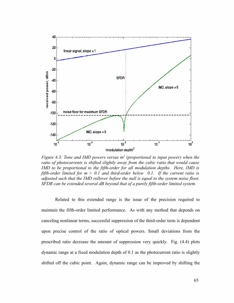
Related to this extended range is the issue of the precision required to
maintain the fifth-order limited performance. As with any method that depends on
canceling nonlinear terms, successful suppression of the third-order term is dependent
upon precise control of the ratio of optical powers. Small deviations from the
prescribed ratio decrease the amount of suppression very quickly. Fig. (4.4) plots
dynamic range at a fixed modulation depth of 0.1 as the photocurrent ratio is slightly
shifted off the cubic point. Again, dynamic range can be improved by shifting the
65
Figure 4.3: Tone and IMD powers versus m2 (proportional to input power) when the ratio of photocurrents is shifted slightly away from the cubic ratio that would cause IMD to be proportional to the fifth-order for all modulation depths. Here, IMD is fifth-order limited for m > 0.1 and third-order below 0.1. If the current ratio is adjusted such that the IMD rollover before the null is equal to the system noise floor, SFDR can be extended several dB beyond that of a purely fifth-order limited system.

ratio per the discussion above, but Fig. (4.4) illustrates just how tightly controlled
this ratio must be. Overall, the experiments reported in this thesis were only
concerned with simple fifth-order limited operation, not exploring the largest
attainable SFDR.
4.4 Experiment
Two 20-mW telecom-grade distributed feedback (DFB) lasers with linewidths of
approximately 2 MHz were used as sources for the link, and amplified with
66
Figure 4.4: 1Hz Dynamic range variation with small deviations of the TM:TE photocurrent ratio from that prescribed in (4.15). The dynamic range can be increased by shifting the ratio slightly, causing multiple distortion orders to be simultaneously suppressed. The exact condition for this to occur changes with modulation depth; here m = 0.1 to match the scenario from Fig. (4.3).

polarization-maintaining erbium-doped fiber amplifiers having an optical noise figure
of 4.5 dB. One wavelength (λ=1554.94 nm) was launched conventionally into the
slow axis of a polarization-maintaining fiber (PMF), which was coupled to the
vertical, or TM, axis of the optical phase modulator. The other wavelength (λ
=1552.52 nm) was launched into the fast axis of a PMF via a 90o splice, polarization
multiplexed within a polarization-maintaining coupler, and ultimately fed into the
horizontal (TE) axis of the modulator, as depicted in Fig. 4.1(b). Thus, each axis of
the modulator was illuminated with a different wavelength, with >24 dB of isolation
measured between the axes at the modulator input and no active polarization control.
The modulator output consisted then of two orthogonally-polarized wavelengths, each
modulated to a different depth owing to the anisotropic electrooptic coefficients for
the z and x axes of LiNbO3.
There is no specific amount of polarization isolation or spectral isolation
required to achieve suppression of the third-order distortion. Suppression is
dependent on the existence of two different modulator transfer functions; any
difference will allow suppression to occur, albeit with different gain. Imperfect
isolation between the two wavelength or polarization states in the system modifies the
effective value of γ and can be compensated by adjusting the power splitting ratio at
the receiver per (4.15), with a change in SFDR in accordance with (4.17), (4.24), and
(4.25).
The modulator was a commercial z-cut, Ti-indiffused LiNbO3 phase
modulator with PMF input pigtail and SMF output pigtail, and a Vπ of 3.25 V at 5
GHz for the TM polarization. Nominally, the Vπ for the TE axis should be
67

approximately three times larger, but was experimentally measured to be
approximately 4.25 times larger in this device. It is possible that the lower than
expected modulation efficiency for TE polarization may be a result of increased TE
mode size within the Ti-diffused waveguide, resulting in a lower overlap between the
RF and optical fields. The ability to use singlemode fiber between the transmitter and
receiver exists because the two signals exist on separate wavelengths that can be
separated with polarization-independent components.
At the receiver, the wavelengths were separated in a commercial WDM
demultiplexer. Variable optical attenuators (VOAs) were used on each wavelength
after wavelength demultiplexing but prior to demodulation to achieve the desired
ratio of photocurrents dictated by (4.15).
Two asymmetric-delay MZIs were used to convert phase to intensity
modulation in the receiver. The MZIs here were thermally-tuned all-fiber devices
with a 100-ps relative group delay between the arms. Both MZIs were thermally
biased at quadrature and the two complementary outputs were detected through a
balanced photodiode pair. The output RF signals were subtracted at the delta output of
the 180o RF hybrid, which had a 2-18 GHz bandwidth. Equivalently, the MZIs could
be set to opposite bias points and the summation output of a hybrid could be used.
The photodetectors were identical balanced detectors with internal 50 Ω resistors and
a 1-dB compression current of 7-mA per diode.
As detailed in [9], the MZI has a periodic transmission function, which limits
microwave frequency range over which it can be used to demodulate the signal. For
the 100-ps MZI biased at quadrature, the optimal modulation frequency is
68

approximately 5 GHz in order to satisfy the condition Ωτ = π.
The group delays of the optical paths to each detector were matched to within
2 ps for optimal differential detection and common-mode RIN suppression at each
wavelength. This was accomplished with a microwave network analyzer providing
input frequency sweep to the modulator, with the photodetector output serving as the
analyzer input. The delay for one path was measured and then the other path(s) was
(were) adjusted to match. Fine adjustments to the path length were made with an
optical variable delay line, although a microwave delay line could equivalently
provide the requisite matching. The RF output from each balanced detector through
the delta port of the hybrid was balanced to within five degrees of 180o for IMD
suppression. Equalizing the delays in this way can also compensate at a single
frequency for the birefringent group delay difference between the TE and TM
polarization states in the electrooptic modulator, which could become significant at
higher frequencies and for longer device lengths.
4.5 Results
Results from two-tone testing with tones at 4.7 and 4.9 GHz are shown in Fig. 4.5.
The squares are the measured fundamental tone and IMD powers for TM modulation
only, at a DC photocurrent of 6 mA per detector. For this measurement, the TE
wavelength was fully blocked at the receiver.
69

Similarly, the circles show the measured results when the link is linearized.
For this setup, the TE wavelength’s power was adjusted to give 6 mA of dc
photocurrent per diode, and the TM optical power was attenuated until the IMD
measurements varied with a slope of five on a log–log plot, indicating fifth-order
limited performance. Had the modulator’s γ been 1/3, the TM optical power should
have been the expected 13 dB below the TE power. Because of the different γ,
70
Figure 4.5. Plot of measured and calculated signal and IMD powers for TM-only (blue squares) and linearized (green circles) configurations, showing third-order suppression. The fundamental tones are 4.7 and 4.9GHz. The lines indicate the expected (calculated) results, adjusted for the experimentally determined electrooptic ratio γ and excess RF loss. All measurements were performed with a resolution bandwidth of 10 kHz.

however (determined earlier to be 1/4.25), the actual TM optical power was 18 dB
below the TE power. Additionally, the RF gain was measured to be 12.5 dB below the
TM-only measurement, in contrast to the expected 10.5 dB.
The output noise power spectral density was measured to be 155 dBm/Hz, and
primarily limited by phase noise of the source lasers and EFDA Amplified
Spontaneous Emission (ASE) that gets fully maximally converted to intensity noise in
the MZIs at quadrature bias [33,34]. The balanced detectors suppress the intensity
component of common-mode noise but the MZIs expose the phase component [34],
which cannot be suppressed by balanced detection. Narrower linewidth source lasers
and no EDFA, as demonstrated in [9], could reduce the phase-to-intensity noise.
When the experimentally determined γ of 1/4.25 and approximately 6 dB of
excess RF loss are accounted for, the measured data agree well with the calculated
predictions plotted as curves in Fig. (4.5).
Table 4.1 summarizes the measured and calculated performance metrics in
columns 1 and 2, respectively, for both TM-only and linearized configurations. The
measured improvement in SFDR due to suppression of the third-order term in the
IMD was 15 dB, in agreement with theory when the 6 dB excess loss is taken into
account. The measurement bandwidth was 10 kHz, although the SFDR has been
normalized to a 1-Hz bandwidth for ease of comparison to other links.
71

TABLE 4.1
MEASURED AND PROJECTED LINK PERFORMANCE
Measured Calculated if γ = 1/3 high-perf.Vπ (volts)γ iDC (mA)shot limited?
3.251/4.25
6N
3.251/4.25
6N
3.251/36Y
11/340Y
TM-only:gain (dB)IIP3 (dBm)SFDR (dB/Hz2/3)
-1511
101
-1413103
-813111
193
116
Linearized:gain (dB)IIP5 (dBm)SFDR (dB/Hz4/5)
-2816115
-2719117
-1817128
97
134
From Fig. 4.5, one can see that despite the penalty in net link gain, the
dynamic range of the linearized system always exceeds that of the conventional
system. In the linearized case, the intermodulation products exhibit a fifth-order
dependence on the input power, and therefore the improvement in SFDR over the
third-order case decreases with increasing noise bandwidth. For the experiments
reported here, the SFDR improvements for 1-MHz and 100-MHz noise bandwidths
were 7 and 4 dB, respectively. Experimental limitations prevented us from verifying
that the intermodulation distortion remains fifth-order limited at powers below the 10-
kHz noise floor. Column 3 lists the calculated performance had the link achieved the
shot-noise limit, had γ been the nominal 1/3 as was expected for LiNbO3, and
removing the excess RF loss.
As a further exercise, performance has also been calculated in column 4 of the
table for a link with state-of-the-art components that have recently become available.
72

Desired high-performance device characteristics include sufficiently narrow linewidth
sources to ensure phase-to-intensity noise is below the shot noise limit, a modulator
Vπ of 1 V (and γ=1/3), and balanced detectors (with internal 50-Ohm resistors)
capable of 40-mA dc current per detector. With this link, the linearized SFDR would
improve to 133 dB/Hz4/5 in the shot-noise limit.
4.6 Conclusions
The system described in this Chapter provides a relatively simple receiver
architecture in comparison to the heterodyne receiver of Chapter 3. An important
feature of this receiver architecture is that the relative powers of the TE and TM
polarizations can be adjusted at the receiver in order to achieve and maintain
linearization, with no additional control or complexity at the transmitter. Unlike the
approach from Chapter 3, in which a single input wavelength was polarized at an
oblique angle to the modulator axes, this method uses an input PM fiber that is co-
aligned with the waveguide. Moreover, the dual-wavelength scheme greatly facilitates
separation of the two polarization states at the receiver and allows standard single-
mode fiber (SMF) to be used between the modulator and receiver.
73

5 Dual-wavelength link with downconversion
I've gotten a lot of results; I know thousands of things that won't work.
–Thomas Edison
5.1 Original dual-wavelength scheme
This Chapter details the theory and experimental attempts to linearize a link utilizing
two wavelengths, similarly to the MZI detection link presented in Chapter 4, but
using heterodyne detection as in Chapter 3 to achieve frequency downconversion
(which the MZI detection could not intrinsically do). This particular technique was
not successfully demonstrated because of an inability to sufficiently stabilize the two
separate optical signals relative to one another to effect a stable recovered IF signal.
This does not, however, preclude its possible future implementation, and the theory
and experimental description are therefore presented here.
5.1.1 Theoretical analysis
Although the variation of optical phase with the input signal voltage is completely
linear, an infinite number of harmonic sidebands (the harmonics) are generated in the
frequency domain. In a real information-bearing signal with more than a single
frequency component, the various summations of all of these harmonics exist and are
collectively known as the intermodulation distortion (IMD). All of these products
exist at the moment of modulation; this is an important point not often made clear in
74

the literature. If a linear optical phase detector were available, one could ignore the
frequency distortions and simply track the optical phase as it linearly varied with the
input signal. As this is not the case, one is forced to look at the frequency
components generated, and the beating of all of these against some common
unmodulated frequency in a square-law detector. This beating reveals the individual
frequencies and is the reason that the pre-existing distortion frequencies are seen in
the recovered signal. Proper filtering and choice of LO frequency can ensure that
only the fundamental (first) sideband is ultimately received (either upper or lower).
Unfortunately, for any multi tone signal, the (2Ω1-Ω2) and (2Ω2-Ω1) permutations fall
within the bandwidth of the fundamental signal and cannot be filtered off. It is this
third-order distortion that must be dealt with now.
A simplified analysis showing how to achieve both linearization and
downconversion is presented as follows: the input RF signal at microwave frequency
Ω is represented as a sinusoid
v t = V 0 sin t (5.1)
and the input optical field to the modulator as
E t = z E1 e j1 t x E2 e j2 t (5.2)
where ω1 and ω2 are the two distinct optical frequencies launched into the modulator
in the same manner as illustrated in Fig. 4.1(b). For reference, the z-axis of a z-cut
modulator is the TM mode, while the x-axis is TE. Neglecting birefringence and
insertion loss of the device, the optical field of the phase-modulated output signal is
75

given by
E out t = z E1 e j 1 tmsin t x E2 e j 2 tmsin t (5.3)
where m = πV0 / Vπ(TM) is the modulation depth for the TM wavelength, with Vπ being
the voltage required to effect a 180 degree optical phase shift in the TM polarization.
The modulation depth of light on the TE axis is given by γm.
Applying the Bessel function expansion to (5.3) and neglecting all but the first
upper sideband gives:
Eout t = z E1 J 1me j 1 t x E2 J 1me j 2 t . (5.4)
As in Chapter 4, each polarization is also a different wavelength and is demultiplexed
in the receiver and then detected separately. Therefore the relevant field incident
upon each of the photodiodes is:
E PD1t = E1 E1LO J 1me j IF1 t
E PD2t = E2 E 2LO J 1me j IF2t (5.5)
If the intermediate frequencies are identical, these two signals can ultimately be
combined as one. Taylor expanding the magnitudes in (5.5),
E PD1t = E1 E1LOm2− m3
16 ...
E PD2t = E2 E2LOm
2−
m3
16 ...
(5.6)
shows the individual terms within the sideband that are proportional to different
76

powers of the modulation depth. The third-order terms can be eliminated by
combining the two signals, setting them equal and of opposite sign to each other:
E1 E1LOm3
16 E2 E2LO
m3
16= 0 . (5.7)
The optical power incident on either of the photodiodes is |EnEnLO|2 and when
multiplied by the detector's responsivity becomes the detector's DC photocurrent.
Similarly to Chapter 4, third-order distortion can be eliminated when the following
condition is met:
−i1
i2= 3 . (5.8)
For LiNbO3 with γ ~1/3, the ratio between the received TM and TE powers is
therefore ~-14dB. This "almost 95/5 split" is the same result from MZM-based
linearization techniques and from Chapter 4. As in the previous Chapter, one of the
primary advantages of using a separate wavelength for each modulation depth is that
they can be filtered and separately controlled in the receiver. Thus the requisite ratio
of photocurrents can be achieved by adjusting the optical powers of the two
wavelengths at any point after demultiplexing, as shown in Fig. (5.1). The received
RF power of the linear signal is reduced from that of a TM-only modulated signal by
the same amount as in the MZI-detection method from Chapter 4, 1−22.
When γ ~1/3 as is the case for lithium niobate, the received signal power is
reduced by approximately 10.5dB relative to the TM-only case. The best-case ratio
results in minimized desensitization to the signal of 8.3dB in a material where γ = 3-
77

1/2, just as in Chapter 4.
An analysis similar to that presented in Chapters 3 and 4 shows the same
result for a two-tone microwave signal. By including higher-order terms, it is
possible to find conditions that suppress any other single order of distortion for all
modulation depths, or that suppress multiple orders of distortion for a single
modulation depth.
5.1.2 Experimental setup
Figure (5.1) is a simplified representation of the link architecture. Both wavelengths
are present for linearized operation as in the MZI experiment, but the powers from
each source are split to create a LO and signal path. Instead of relying on polarization
angles to present the proper ratio of modulated powers at the detector as was
previously implemented, the two separate wavelengths of light were launched into
orthogonal polarization axes of a z-cut, Ti-indiffused waveguide LiNbO3 phase
modulator. Each wavelength being modulated differently, they were spectrally
demultiplexed at the receiver and their relative powers adjusted for the proper ratio
prior to detection. Fig. 5.1 shows a differential balanced pair of photodiodes to detect
each wavelength; this would have the benefit of suppressing common-mode noise for
each wavelength. The actual setup only used a single photodiode for each wavelength
to simplify the initial effort and avoid the need to match group delays on four separate
optical paths. After detection and downconversion, the two signals were recombined
in the RF domain with a 180-degree hybrid. The optical paths for each wavelength
were carefully matched to ensure the RF phases were synchronized after detection,
78

but this became the stumbling block of the experiment, as will be seen. By adjusting
the power ratio at the receiver, precise control of the optical powers in the link itself
was not required, containing complexity within the receiver and not throughout the
link, similarly to the link design from Chapter 4.
In this embodiment, part of each source laser was split off, multiplexed,
passed through an acousto-optic frequency shifter and then amplified to generate a
heterodyne LO, similarly to the original experiment reported in Chapter 3. A single
AOM was used to ensure that both wavelengths were offset by the same frequency.
As long as the path difference between the signal and LO legs was well within the
coherence length of the sources, could be kept steady over a reasonable time scale,
and the AOM itself did not impart significant phase noise to the LO leg, RIN from
phase-to-intensity noise conversion will not be a factor. If a separate source were
used for the LOs, the phase-intensity RIN would have to be very carefully managed,
possibly requiring extremely narrow linewidth lasers.
79
Figure 5.1: Schematic of the proposed research link. For clarity, polarization controllers in the receiver are not shown.
5.1.3 Results and lessons learned
The link was built as illustrated in Fig. (5.1), but using a single photodiode to detect
each wavelength to simplify the initial attempt. The group delay for each wavelength
was matched by using a RF network analyzer to measure the group delay/phase
mismatch of one path relative to the other. The analyzer's output (RF input to the
optical link) was modulated onto the optical carrier by substituting a MZM for the
phase modulator, and then the AOM (which was temporarily removed to allow this
path matching), which provided intensity modulated light at the photodetectors. The
received signal was then fed to the network analyzer's input. Using this technique, the
RF phases for each wavelength's leg (signal and LO for each) were matched to within
two degrees from 10MHz through 12GHz. Conversely, their output phases were 180
degrees out of phase after the signals were passed through the RF hybrid.
The modulator used in the experiment from Chapter 4 was reused here, and
the AOM was the same device as the one used in the experiments in Chapter 3.
Single-wavelength heterodyne detection using two test signals at 1250MHz and
1275MHZ, with the detected IF at 250MHz and 275MHz, respectively, verified the
modulator's measured Vπ(TM) = 3.2V at 1250MHz. This was measured two ways, as
detailed in Appendix A. Similar measurements with the second wavelength launched
onto the TE axis verified that the Vπ(TE) was approximately 14V, which made γ =
1/4.4, agreeing with the measurements from Chapter 4. According to eqn. (5.8), to
achieve linearization, the detected TE to TM photocurrents needed to be in a nearly
84:1 ratio, or a received optical power difference of more than 19 dB.
The output IF signal (and its attendant IMD) for each single-wavelength path
80

was stable both in magnitude as observed on a RF spectrum analyzer and in phase as
observed on an oscilloscope. When both wavelengths were on and the expected
current ratio was approached, the 225MHz and 300MHz IMD products' magnitudes
began to fluctuate by 10 dB or more, and the IF tones themselves were varying
slightly in amplitude. This indicated that third-order suppression might be taking
place, but the signals were not stable enough to ensure the 180-degree phasing needed
to suppress the distortion.
To verify this, a single tone was modulated onto both wavelengths. The IF
output from each wavelength's photodiode was displayed on an oscilloscope, and the
display was self-triggered from one of the inputs. If the phase relationship between
81
Figure 5.2: Unstable IF phasing between wavelengths. Oscilloscope screen capture showing unstable phase relationship between wavelengths. Trace was captured after approximately ten seconds' run.

the two signals were constant, the second input's trace would appear steady with some
fixed (ideally zero, if the paths are properly matched) phase offset from the first trace.
As is apparent in Fig. 5.2, the second wavelength's trace is not at all stable relative to
the first. This capture shows the display is completely filled in after 10 seconds of
capture, indicating that the second trace is “walking” very rapidly in relation to the
first trace.
There were several potential sources for this: very large laser linewidths, a
very unstable AOM generating a noisy LO, or optical paths that were not stable
enough to ensure the relative optical phases were maintaining a steady relationship.
The most likely source was primarily from unstable path lengths. Several
modifications were made to the link to mitigate this problem. The original lasers were
found to have a permanent coherence control function that increased their linewidths
to ~100MHz. These were replaced with external cavity lasers having <50kHz
linewidths, and the AOM driver was replaced with a high-purity synthesizer and
narrow bandpass filter to ensure only the desired frequency was present in the AOM.
Neither of these modifications made any measurable improvement in the relative
phase stability of the received IF signals.
The receiver itself was then modified to the configuration in Fig. 5.3. This
method, although preventing the possibility for balanced detection of each
wavelength, helped ensure that each signal-carrying wavelength would travel along a
common fiber path through as much of the link as possible until just before detection.
This design mitigated the chance of slight environmental perturbations on one
wavelength's path to change the path length and therefore the optical phase and
82

recovered signal phase. To further improve the interferometric stability of the
receiver, it was securely packaged in foam to thermally and vibrationally stabilize the
receiver.
This receiver did not use the available optical power as efficiently as the
original setup, since a polarization controller and then linear polarizer was needed
between the phase modulator and mixing coupler to ensure that some component of
each (orthogonally polarized) modulator output was co-polarized with the LO leg to
allow the heterodyne mixing to occur. In principle, this could also be used to set the
necessary optical power ratio to linearize the recovered signal.
The received output from each wavelength's photodiode was sent to an
oscilloscope as before and similarly compared, with typical results shown in Fig. 5.4.
There was significant improvement, but even with a well-insulated receiver utilizing
as much common-path design as possible, the two separate wavelengths with their
signals could not be sufficiently stabilized to reliably linearize the link.
83
Figure 5.3: Modified design for dual-wavelength linearized down-converting link, minimizing the separate paths to increase phase stability between the wavelengths.

It became apparent after this level of effort that significant complexity and
care would be needed to further stabilize the two paths enough to demonstrate more
than fleeting linearization. Doing this would violate the overarching goal of the
project: to develop a fairly simple technique for linearization that required minimal
control and that could feasibly be utilized in a real-world application. Thus, another
method was needed that would reliably convert phase to intensity modulation, down-
convert, be linearize-able, and show promise for rapid improvement and
productization. A key to this would be to find a method that could be insensitive to
laser or LO phase noise and did not require interferometric stability in the receiver.
84
Figure 5.4. Oscilloscope screen capture of modified receiver IF output showing significantly improved phase stability at 250MHz, with infinite persistence and captured after approximately one minute of run.

6 Alternate method for a linearized phase-modulated fiber optic link with downconversion, for K-band microwave signals
After the problems encountered with stabilizing the output of the Chapter 5 design, it
became apparent that a different method was needed to be able to reliably linearize
and down-convert a signal. The previous link used an acousto-optic frequency shifter
to generate a local oscillator at 1 GHz, and was not successful at that offset frequency.
The intended frequency band, however, is the SATCOM and terrestrial point-to-point
regime: X (8-12 GHz), Ku (12 -18 GHz), K (18 – 27 GHz), and Ka (27 – 40 GHz)
bands.
Once the problem was re-scoped to focus on recovering signals above ~10
GHz, a completely new receiver approach became apparent [98]. The new method
uses the same transmitter/modulator configuration as in Chapter 4. A single
conventional lithium niobate phase modulator is still at the transmitter, which
modulates two different wavelengths on orthogonal polarizations that travel along a
common fiber path.
The new receiver is a significant departure from the previous ones. The
wavelengths are modulated again in the receiver to impart a local oscillator tone near
the signal, then the closely-spaced upper sidebands are filtered with a fiber Bragg
grating (FBG) to present the beat IF between the LO and signal at the photodetector.
The receiver in this link does not require a second frequency-locked laser to generate
the local oscillator which reduces complexity by allowing direct detection using only
the incident optical power at the receiver. Phase stability between the signal and LO
is also assured since they share the same underlying optical carrier and a common
85

path. For linearized operation, all adjustments can be made at the receiver, removing
constraints on optical power ratios in the link itself.
The link presented in this section automatically down-converts the signal to
the desired IF, and the signal can be linearized to suppress the third-order
intermodulation distortion (IMD) which increases the sub-octave spur-free dynamic
range (SFDR). The downconversion technique shares some conceptual similarities
with several previously reported methods [84,85,96,99] but is adapted to allow direct
detection of a down-converted phase-modulated link by filtering a single optical
sideband for direct detection. Optical sideband filtering allows only the IF to be
detected, and has been used in IMDD links to mitigate chromatic dispersion penalties
[100]. A variation that partially suppresses the carrier has been used to improve the
noise figure and SFDR of a link [94,101], but filtering has never been used to
explicitly allow detection of a phase-modulated link. Recent work shows another
variation of this method, using the edge of the FBG filter passband as a frequency
discriminator to then detect frequency-modulated optical signals [102-109].
The limitation on the method presented here is that the optical filter must be
able to provide significant rejection between the signal sideband and its carrier and
other sidebands, placing a practical lower frequency limit at a few GHz with
conventional filter technology (e.g. FBGs). Thus this link works most effectively at
higher GHz frequencies, where it becomes easier to spectrally filter the sideband
using off-the-shelf WDM filter components designed for narrow channel spacing.
Fortunately, the burgeoning applications utilizing the K and Ka bands (18-40 GHz) fit
this criteria perfectly.
86

6.1 Concept
Fig. 6.1(a) shows the layout used for this experiment. The high-frequency RF signal
(near 20 GHz for this experiment) is phase modulated onto an optical carrier. At the
receiver, the optical signal is amplified and then phase modulated again, this time
with a very strong single microwave tone near 20 GHz frequency. Illustrated in Fig.
6.1(b), this tone is placed near the signal of interest and follow-on spectral filtering
rejects all other products, leaving only the LO tone and the original signal to be
recovered. Since the lower sideband has been removed by the optical filter, the beat
between the LO and signal at the desired intermediate frequency (IF), typically
between 50-300MHz, is directly detected by a photodetector. The detector only
requires enough bandwidth to cover the IF range, significantly lowering the
component cost of the link and enabling higher current-handling capability.
87

As the signal and LO frequencies gets higher, it becomes easier to spectrally
filter the desired sideband without concern for very tight filter edge tolerances or
stability. Although custom or even commercial FBGs can be made to effectively
filter lines with only a few GHz separation, the task is much easier when 20 GHz or
more of spacing is available. The linearization technique used here is the same as
what was used in Chapters 4 and 5. A different wavelength is again used for each
88
Figure 6.1: (a) Schematic diagram of dual-wavelength linearized down-converting phase-modulated link. (b) Notional spectrum, describing the LO and filter placement relative to the signal and carrier. (c) For linearized operation the two wavelengths are polarization multiplexed and launched along the TM and TE axes of the modulator.

polarization in the modulator, and each is separately recovered with the filtered
sideband method and the detected currents combined in the proper ratio to effect
linearization.
6.2 Nonlinearized (TM-only) link characteristics
A single-wavelength link using the normal modulator polarization will be examined
first, to determine the behavior of the conventional, non-linearized link which will
serve as a basis for comparison. The optical carrier is phase modulated with the RF
signal, generating the usual spectrum:
E t = P0 e j t ∑n=−∞
∞
J n m s ej n s t . (6.1)
P0 is the optical power before spectral filtering, ms is the signal modulation depth
defined again as ms = (πV0s)/Vπ(TM), ω is the optical frequency, and Ωs is the
microwave signal frequency. V0s is the peak voltage of the modulating signal.
The field from (6.1) is presented at the input of the second phase modulator.
The Local Oscillator (LO), with frequency ΩLO, is a single microwave tone
modulating this field, and the output of the second modulator (ignoring device
insertion loss) is the combination of both the signal and LO:
Eout t =P0 e j t ∑p=−∞
∞
∑n=−∞
∞
J pmLO J nmse j pLOns t (6.2)
When the LO is modulated onto the carrier, undesired distortion products are
generated between the LO frequency and all frequencies present in the original signal
89

and its sidebands, according to (6.2). This is IMD between the signal and LO, and is
not the IMD created by multiple signal frequencies we are primarily concerned with,
as is shown below.
The products around the upper optical sidebands occurring between the
optical carrier ω and and twice the signal frequency (ω + 2ΩS) are enumerated as
follows (n and p are the integer indices from 6.1 and 6.2), and illustrated in Fig. 6.2:
LOinteracting withthe carrier :P0 J 0mLO J 0 mse
j t
P0 J 1mLO J 0msej LOt
P0 J 2mLO J 0msej 2LO t
LOinteracting withthe signal upper sideband :P0 J 0mLO J 1mse
j s t
P0 J 1mLO J 1msej sLO t
−P0 J 1mLO J 1m sej s−LO t
LOinteracting withthe signal upper harmonic:P0 J 0mLO J 2mse
j 2st
−P0 J 1mLO J 2msej 2s−LOt
P0 J 2mLO J 2msej2s−2LO t
LOinteracting withthe signal lower sideband :−P0 J 2mLO J 1mse
j −s2LOt
(6.3)
90

The products below or near the optical carrier frequency and above or near
(ω+2ΩLO) are optically filtered by the FBG, and the only remaining products of
concern are those close to the LO and signal frequencies:
E t = P0 J 1mLO J 0msej LO t
P0 J 0mLO J 1msej s t
−P0 J 1mLO J 2msej 2 s−LOt
−P0 J 2mLO J 1msej − s2LOt
(6.4)
This is recognizable as two tones and their IMD terms at (2Ωs-ΩLO) and (2ΩLO-Ωs).
91
Figure 6.2: Spectrum of signal, LO, their harmonics, and intermodulation products between the optical carrier and the second harmonic of the signal. Black products are the LO interacting with the carrier. Red is the LO interacting with the signal USB, green with the LSB, and blue with the signal's second harmonic. The signal modulation depth is 0.1; the LO modulation depth is 1.08.
Upon squarelaw detection the Ωs term is down-converted to ΩIF, (2Ωs -ΩLO) to 2ΩIF,
and likewise the (2ΩLO-Ωs) term appears at -ΩIF. The 2ΩIF term is electrically filterable
as long as the signal bandwidth is smaller than the IF (i.e. the signal is sub-octave at
the IF). Sub-octave bandwidth at the IF is generally the case; one example is DVB
“satellite TV” systems which transmit a 500 MHz bandwidth in the X- or Ka-bands
and are downconverted in the receiver to a 950 or 1150 MHz IF for local distribution
over coaxial cable. The signal bandwidth is approximately half of the IF.
A more difficult problem is the term at (-ΩIF) which gets wrapped back onto
ΩIF in a squarelaw detector and, having opposite amplitude, serves to reduce the IF
amplitude by [J2(mLO)J1(ms)]. The net IF amplitude from (6.4) becomes
E t = P0 J 0mLO J 1ms−J 2mLO J 1ms e j t e j s t (6.5)
This is a power penalty to the signal of < 0.17 dB for ms ≤ 0.1 and mLO = 1.08
(this depth is used for reasons explained below), relative to the power had the IMD
not been present, and can be ignored for low signal strengths.
An interesting situation occurs if the input field to the LO modulator is
prefiltered so only the carrier and first signal USB are present. The (2Ω-ΩLO) product
is generated in (6.2) by multiplying the second harmonic of the signal with the LO's
first lower sideband, and the (2ΩLO-Ω) product similarly comes from the LO's second
harmonic and the signal's first lower fundamental. If the signal's second upper and
first lower sidebands are not present when the LO tone is modulated, then the new
IMD products will not be created, analogously to the situation of using a quadrature-
biased MZM to generate a LO, when there are no second harmonics in either the
92

signal or LO [99]. Although this requires a second optical filter to be placed in the
fiber path prior to the LO modulator, this adaptation could be useful if the (usually
small) reduction in the received IF signal cannot be tolerated.
If we assume a small signal modulation depth and sub-octave bandwidth at the
IF, we can ignore and filter the small penalty caused to the IF by IMD between the
LO and signal. The input to the photodetector after optical filtering is (6.4) and the
detected photocurrent is only from the LO and signal themselves:
i t = ℜP0∣ej t J 1mLOe
jLOt J 0mLO J 1msejs t∣2. (6.6)
The DC current is generated by the LO, which is a component of the original
optical carrier that acts as the surrogate carrier. Assuming zero passband transmission
loss through the filter,
iDC = J 12mLOℜ P0. (6.7)
The relevant received current becomes
i t = ℜ P0 [ J 12 m LO J 1 mLO J 0m LO J 1m s 2cos IF t ] (6.8)
where ΩIF is the IF frequency (Ω-ΩLO) and J12(ms) to be very small. When
substituting (6.7) in and allowing J1(ms) ~ ms/2 for small modulation depths, the
current becomes
i t = i DC [1 J 0 mLO J 1 mLO m s cos IF t ] . (6.9)
93

6.2.1 Optimizing the signal
Upon examination of (6.7) and (6.8), the carrier and signal have different
dependencies upon the LO modulation depth. There is an opportunity to maximize
the received signal current amplitude and therefore received RF power by adjusting
the LO modulation depth. If mLO is set to maximize the product J0(mLO)J1(mLO) from
(6.8), the argument mLO becomes ~1.08 as shown in Fig. (6.3). This results in a
maximum AC signal amplitude and the ratio J0(mLO)/J1(mLO) from (6.9) becomes
1.57 for this argument.
This result is somewhat surprising considering that an argument of mL = 1.83
(where the first-order Bessel function is maximized) would maximize the LO
94
Figure 6.3: Normalized received RF power as a function of local oscillator modulation depth. The signal itself becomes desensitized by J0(mLO) when the oscillator is imposed.
amplitude. Normally this would be thought to result in an optimal signal, analogously
to the “strong LO” case for heterodyne detection. For this link, the LO modulation
depth also significantly affects the signal itself because the LO is modulated onto all
frequencies present, not simply combined with them as in a traditional heterodyne
receiver. The LO and signal are not independent; they are linked by differing
dependencies upon the LO modulation depth. The benefit of a stronger LO is more
than offset by the desensitization caused to the signal itself. There is a second
detriment to increasing the LO power further; the DC current arises from it, and most
noise sources have a direct dependence upon DC current. So maximizing the LO for
this link not only serves to decrease the signal amplitude, but also increases the
received noise.
It is tempting to use only (6.9) in this analysis, which would lead one to
presume differently; that a mLO approaching zero would maximize the RF signal as
the ratio J0(0)/J1(0) grows large. For a given DC current this is true, but one must
remembered that mLO directly affects iDC. Setting mLO to a low value low results in a
small iDC which reduces the received signal.
6.2.2 Link metrics: gain and conversion loss
The small-signal RF gain is the output RF signal power divided by the input RF
power:
95

G RF =⟨ i sig
2 ⟩ Z out
V RF , rms2
Z i =
⟨i DC J 0 m LO J 1m LO m s cos IF t
2 ⟩ Z out
V RF , rms2
Z i
(6.10)
which can be simplified to
GRF = J 0mLOJ 1mLO
2
V 2
iDC2 Z i Z out . (6.11)
This expression is similar to that for a Mach-Zehnder link with the exception of the
lack of a bias phase term in the cosine's argument (since the carrier/LO and signal
have not been offset in phase) and the leading term, incurred because of the LO being
modulated onto all carrier and signal components. For mLO = 1.08 to maximize the
signal for a given input optical power to the FBG at the front of the receiver, the gain
becomes:
GRF = 2.46 V
2
iDC2 Z i Zout . (6.12)
By automatically down-converting the RF signal to an IF, this link design
makes it impossible to strictly separate the frequency conversion loss from the
intrinsic loss (Gain) of the fiber optic link itself. However, a close comparison can be
made versus a 'traditional” quadrature-biased MZM link without downconversion
96

which is preceded or followed by an electronic mixer to generate the IF. A
comparison with a heterodyne detection link will not be made here because of the
additional degree of freedom provided by the heterodyne link's LO power. We will
assume that each modulator has the same VΠ and that equivalent optical powers are
present at each photodetector (e.g. there is an EDFA prior to the receiver to
compensate for the filtered optical power). The RF Gain of the MZM link is given
by:
GRF , MZM = V
2
iDC2 Z i Z out . (6.13)
Comparing this with (6.12), on a milliamp for milliamp of detected current basis, the
gain for this optimized link is 2.46 times greater than that from a MZM link, or
almost 4 dB more received RF power. Furthermore, the output of the link presented
here has already down-converted the original signal, whereas the MZM link still
requires a separate mixer to generate the IF. A survey of mixers capable of
converting signals in the 20-40GHz range to an IF in the VHF band found most
conversion losses to be between 7dB and 12dB. When this is taken into account, the
filtered sideband link outputs a 11-16 dB more powerful IF signal than a MZM link.
Another way to understand this increased efficiency is to realize that the
“effective” modulation depth at the detector is larger than it would be if the signal
were being measured against the original carrier. The LO, which has replaced the
carrier, is of smaller amplitude than the original carrier. Modulation depth can be
seen as a measure of the ratio between the signal and carrier; that ratio is closer when
the LO is used to compare against than the real carrier.
97

It is important to note that the gain comparison with a MZM link is based
upon the received photocurrent, not the available optical power. In a MZM link all
the optical power in the fiber (ideally) is contained in the carrier and sidebands, and
contributes to received photocurrent. The link presented here filters off a large
fraction of that same optical power. The only power incident upon the detector is that
portion contained in the first signal and LO upper sidebands.
If one considers the “receiver” input for this link to be at the FBG input, it is
clear that the MZM link uses the optical power more efficiently. An optimized filtered
sideband link appears to suffer approximately 9.4dB more RF-to-RF loss than a
comparable MZM link when mL = 1.08, although this loss is in line with the loss the
MZM link must go through in an electronic mixer, making the links roughly
comparable in final IF gain. The availability of high-gain EDFAs to serve as a
receiver preamplifier has somewhat mitigated the need to be particularly efficient
about utilizing the optical power coming in from the remote link fiber, so a
comparison using the power actually incident upon the detector (i.e. the photocurrent)
is a fair one. In this context the link presented here is more efficient than the MZM
link in terms of RF small-signal gain.
6.2.3 Link metrics: noise
There are six noise power terms that must be known to continue determining the link
performance: input and output thermal noise, laser RIN, shot noise, EDFA signal-
spontaneous and spontaneous-spontaneous beat noises. Input thermal noise is the
fundamental limit on link sensitivity, but is generally swamped by the additional
noise sources for achievable modulator efficiencies [40,110]. The other noise power
98

spectral density terms were described in (2.3) and are repeated here:
S0, thermal = k B TS0, laser RIN = ⟨ iDC
2 ⟩ Zout RIN laser
S0, shot = 2e ⟨ iDC ⟩ Zout
S0, ssp = ⟨ iDC2 ⟩ Zout2hNF EDFA
Popt , i S0, spsp = ⟨ iDC
2 ⟩ Zout 2h NF EDFA
Popt , i 2
Bo
(6.14)
where kB is Boltzman's constant, T is the absolute temperature of the receiver, RINlaser
is a measured quantity, e is the fundamental electron charge, h is Planck's constant,
ν is the optical frequency, NFEDFA is the optical noise figure of the amplifier, Popt, i is
the optical power at the EDFA input, and Bo is the optical bandwidth incident upon
the receiver. With these noise terms, the remaining metrics for link performance can
be determined. The RF noise figure is defined as the ratio of the received noise to the
input thermal noise (kBT) times the system gain:
NF RF =S 0
GRF k B T (6.15)
where S0 is the total received noise power spectral density, the simple sum of the
terms in (6.15).
6.2.4 Optimizing noise figure
The different dependencies of the DC and signal currents upon LO modulation depth
also allow the signal-to-noise ratio to be maximized, conversely the noise figure to be
minimized. Contrary to the previous analysis that maximized the RF signal, NF
99

decreases as the LO modulation depth decreases as long as there is enough DC
photocurrent from the LO to remain above the thermal noise limit. In the shot-noise
limit, noise power increases linearly with DC current as discussed in section 2.3.1 and
reviewed in the previous section. In the EDFA beat noise or laser RIN limit, noise
power increases quadratically with DC current. Qualitatively these cases make sense,
since the AC signal is the only product present at the detector as the LO becomes
small. Of course, as the LO vanishes there is nothing for the signal to beat against
and no information can be recovered. Fig (6.4) shows the general dependence of
noise figure upon the local oscillator's modulation depth for the shot-noise and EDFA
signal-spontaneous noise limited cases, both becoming thermal receiver noise limited
as iDC decreases. Note that thermal noise again dominates as mLO approaches 3.83, the
first zero of J1.
Although the signal-spontaneous limited NF is at a minimum when mLO ~
0.14 and the shot-limited NF is minimized for mLO = 0.5, practical considerations in
the link may make these unrealistic operating conditions for experimental purposes.
The RF gain in the experimental setup was too low (largely because of the high Vπ of
the signal modulator) and there was no measurable IMD with achievable input
powers. For this reason, the preferred operating condition for this link was to
maximize the RF signal power (mLO=1.08) and ensure measurable IMD.
100

6.2.5 Link metrics: filtering
The optical filtering is not perfect; remnants of the optical carrier and its lower 1st
sideband and harmonics may remain and contribute to the received DC current.
Therefore the measured DC photocurrent is greater than it should be, and conversely
the “useable” DC current that is available to multiply the signal term in (6.8) is
smaller than the entire DC current. The portion of the received DC current that is
useable by the AC term is that fraction of the total current caused by the LO's 1st
101
Figure 6.4: Relationship of system noise figure to LO modulation depth for shot-noise and EDFA signal-spontaneous noise cases, including receiver thermal noise which dominates as the LO becomes too small to generate ~1mA of current. For this calculation, the modulator Vπ was set to 1V. Laser RIN follows the same behavior as EDFA noise.

upper sideband:
mL =J 1
2mL
J 12mL0 J 0
2mL1 J 12mL2∑
n=2
∞
n J n2mL
. (6.16)
αn is the filter attenuation of that particular optical frequency, a measured quantity for
each spectral component passing through a particular filter.
The received current thus becomes
i t = iDC [1mLO J 0mLOJ 1mLO ms cos IF t ] . (6.17)
and the small-signal RF gain for any mLO and Φ is given by:
G RF = 2 m LO J 0 m LO J 1 mLO
2
V 2
i DC2 Z i Z out . (6.18)
If the LO is optimized as discussed above with mLO= 1.08, measurable power
still exists in the carrier as well as the first two sidebands (upper and lower). In
practice, with real filtering, the carrier (J0) will generally have the least attenuation
and largest original amplitudes, and will be the limiting terms. For 20dB constant
out-of-band attenuation with a LO modulation depth of 1.08, K = 0.965 (20dB
rejection is routinely attained with commercial off-the-shelf FBG channel filters).
For >20dB attenuation we can often ignore K for a reasonable estimate, as the penalty
is <0.3dB.
102

6.2.6 Link metrics: SFDR
The sub-octave dynamic range is limited by third-order intermodulation (IMD)
products at (2Ω1-Ω2) and (2Ω2-Ω1) that are naturally created exactly as in the analysis
presented in Chapter 4. As in [65], the input-referenced third-order intercept point for
this non-linearized link is given by:
P IIP3 =42 V
2
Z i (6.19)
and the third-order Spur-Free Dynamic Range (SFDR) by:
SFDR = GRF P IIP3
S 0 B 2 /3
. (6.20)
6.3 Linearized Link Characteristics
The conditions for linearization (suppression of third-order distortion) when two
separate photocurrents that each result from differently modulated optical signals are
present have been set forth in [62] and [111] as well as Chapter 4 for MZM and
phase-modulated links with interferometric detection, respectively. One wavelength
is present on each polarization axis in the modulator, these wavelengths are spectrally
separated by the FBGs, detected separately, and the resulting photocurrents are
subtracted in a RF 180˚ hybrid. When the two currents are combined in the proper
ratio any single distortion order can be suppressed.
Since this link uses a different detection scheme than Chapter four, the
103

linearization condition for this link will be derived here, using a single-tone analysis
that is easily extended to two tones as was done in previous Chapters. From (6.8), the
time-varying signal currents from the TM and TE signals, respectively, are:
iTM t = i DC ,TM [1 J 0mLO J 1mLO J 1ms2cos IF t ]
iTEt = iDC ,TE [1 J 0mLOJ 1mLO J 1ms2cos IF t ] .
(6.21)
γ is the ratio of switching voltages Vπ(TM)/ Vπ
(TE). For Lithium Niobate, γ ~ 1/3. The
modulation depth ms is the depth on the “normal” or TM polarization. The depth for
the TE polarization is reduced by γ since the Vπ along the TE axis is larger by
approximately a factor of three. The term due to the LO modulation depth is the
same for both wavelengths, since we use a polarization controller and linear polarizer
to ensure optical power from both wavelengths input to the LO modulator is aligned
with the TM axis.
Taylor expanding the Bessel functions for the signal,
iTM t = i DC ,TM J 0mLOJ 1mLO m s
ms3
8...cos IF t
iTEt = iDC ,TE J 0mLOJ 1mLO ms
ms3
8...cos IF t
(6.22)
the cubic terms can be eliminated when
iTM =3 iTE (6.23)
104

which is the same result as for the linearized MZM IMDD and interferometrically-
detected phase-modulated links. For LiNbO3, third-order suppression is expected to
occur when approximately 95% of the current is from the detected TE wavelength
and 5% is from the TM wavelength. At this point, the dominant sub-octave distortion
is proportional to m5, the fifth-order.
Just as in Chapter 4, precise control of this ratio is necessary in order to
maintain linearized performance, and the SFDR can in principle be extended by
shifting the ratio slightly away from the cubic relationship. Also as in Chapter 4,
standard WDM components can be used to demultiplex and individually control each
color, and PM fiber is not required on the return fiber between the modulator and
receiver.
Most of the received current is from the “wrong” or weakly-modulated
polarization, and the linearized RF Gain is reduced by:
gain correction= 1−22 (6.24)
which is about 10.5dB lower than the “normal” RF gain from the non-linearized
case, where all the optical power and therefore current is from the strongly-modulated
TM axis of the modulator. In calculating gain here, the iDC is the TE wavelength's
detector current. The RF gain penalty can be seen as having two components: γ2 is the
penalty associated with the dominant signal being from the TE polarized wavelength,
instead of the “usual” TM wavelength and (1- γ2)2 is the penalty due to the fractional
TM wavelength's signal that is in opposition, subtracting from the signal amplitude.
As in Chapter 4, the input-referenced fifth-order intercept point (IIP5) is found
105
by including fifth-order terms in (6.22) when the currents are as according to (6.23).
This yields
P IIP5 =P IIP3
35
(6.25)
and the fifth-order limited SFDR is
SFDR5 = 1−22GRF P IIP5
S 0 B 4 /5
(6.26)
The birefringence of LiNbO3 can cause significant differential group delay
between the signal modulated on the TM and TE axes. In order for the linearization
to work, the IF phases must match. The extraordinary ray's group index in LiNbO3
(TM in a Z-cut device) is 2.14 at 1550nm, whereas the ordinary (TE) index is 2.22.
This can be largely ignored at low signal frequencies as demonstrated in Chapter 3,
but causes significant microwave phase mismatch as the signal frequency increases
into the X- or K-band, and must be compensated for. For instance, a 5cm long
modulator will cause approximately 13.3 ps relative delay, or 95 degrees of RF phase
difference between the TE and TM polarized modes for a 20GHz signal, the TE mode
being retarded with respect to the TM mode.
A method to remove this effect is to insert an identical modulator into the
signal path immediately after the signal phase modulator. This modulator is not
active; it serves as a compensator to remove the birefringent phase delay from the
original modulator. If the signal modulator has a PM output, a 90-degree splice or
106

connection between the two modulators will reverse the axes and remove the
differential delay at its output for all frequencies. The output of this second phase
modulator can be SMF. Similarly, an appropriate length of PM fiber will also remove
the birefringence. An alternate technique is to use a time delay in the receiver on the
TM wavelength after spectral separation, to realign the IF phases.
6.4 Experiment
Two external cavity tunable lasers were polarization multiplexed onto the slow (TM)
and fast (TE) axes of the signal modulator's input PM fiber. as shown in Fig.(6.1).
Although these lasers had fairly narrow (~50 kHz) linewidths, there is no explicit
requirement for particularly narrow/stable lasers because all frequencies present at the
detector share a common carrier and common path. The TE wavelength was launched
onto the fast axis by means of a 90-degree PM splice. Isolation between the two
wavelengths (polarizations), measured at the output of the modulator, was >24dB.
The two RF signal tones were 19.95 and 19.98GHz. Each output wavelength
emerging from the modulator thus carried the same signal, modulated to different
depths.
Less-than-perfect polarization or spectral isolation in the modulator or at the
detectors does not preclude linearization, as long as the net modulation depth on each
wavelength is different. Any imperfections in the polarization multiplexing will
change the effective γ ratio, thereby changing the ratio of received TE and TM
currents needed for linearization according to (6.23) and changing the received Gain
and SFDR per (6.24) and (6.26).
107

The signal modulator in this experiment did not have a PM output fiber so a
compensating modulator was not used to remove the birefringent group delay since
the polarization state between the modulators could not be fully preserved. Instead, a
fiber delay was placed in the TM wavelength's path at the receiver.
The output of the modulator traveled through a length of SMF to a
polarization controller, then into a single-polarization EDFA with a measured 11dB
Optical Noise Figure [38]. Since the two wavelengths may still be largely
orthogonally polarized at the receiver input, the polarization controller was adjusted
to ensure that some significant power from each wavelength was properly aligned
with the single-polarization input to the EDFA, and the polarized EDFA output ensure
that only optical power aligned with the LO modulator's TM axis was launched into
it. This ensured that both wavelengths experienced the same LO strength.
Alternately, a SMF EDFA could be used with a linear polarizer at the LO modulator.
The signal at the LO modulator input was not pre-filtered, a possibility discussed in
section 6.2.
The LO modulator was driven by a single 19.7 GHz tone at a modulation
depth of 1.08 to optimize the received IF signal current, corresponding to an input
power of 18.1dBm. As discussed previously, depth was chosen to ensure measurable
IMD would be present because of engineering limitations of the system components.
For a known Vπ, the RF power to produce a given modulation depth is found, after
some algebraic manipulation of the expressions for modulation depth and RF power,
to be:
108

PRF =1
2z imV
2
. (6.27)
This depth was verified by measuring the difference in power between the optical
carrier and the first optical sidebands on an Optical Spectrum Analyzer, a simple task
as long as the sidebands are more than a few GHz removed from the carrier. For a
modulation depth of 1.08, the J0 carrier will be 4 dB above the J1 sideband, shown in
Fig. 6.5.
Both the signal and LO modulators were 40GHz bandwidth Z-cut, Ti-
indiffused phase modulators, 5cm in length with measured TM Vπ of 7.4V at 20GHz,
measured as specified in Appendix A. The signal modulator's TE Vπ was measured as
20.5V at 20GHz, for a γ of 0.361, or 1 / 2.77.
109
Figure 6.5: OSA screen capture of a 19.7 GHz LO tone, phase modulated onto a 1549.62nm carrier (center of the figure) with a modulation depth of ~1.08, or 18.1 dBm RF power delivered to the modulator. The carrier and sidebands differ by 4 dB.

After both wavelengths were modulated with the LO, they were passed
through thermally stabilized FBGs with nominal 30GHz 1dB bandwidths to separate
out one of the wavelength's upper sidebands (1st sideband of the signal and LO) on the
reflective path. The remainder of the signal was transmitted through the FBG to a
second FBG that selected the other wavelength's upper sidebands. This filtering both
spectrally separated the two signals and effected the IF downconversion by
heterodyne photodetection. The FBGs used in this experiment were not particularly
well-suited to this application; the carrier was only attenuated by 5dB relative to its
power without the FBG in place over the upper sideband, causing Φ from (6.16) to be
0.466, a Gain penalty of 6.6 dB. Fig. 6.6 shows the optical carrier and tone LO
sidebands for one of the wavelengths used, with no filter in place. Fig. 6.7 shows the
same carrier and tone, but with the FBG inserted into the optical path, with a 5 dB
differential change between the carrier and sideband. This penalty more than
cancelled the “improvement” over a MZM from (6.12) and therefore the RF gain of
this particular embodiment was expected to be 2.7 dB lower than that of a MZM link
with the same photocurrent. The first lower sideband, which is in anti-phase with the
upper sideband and would further diminish signal recovery, was attenuated by 18dB
and therefore does not have any significant effect on the results. The upper second
harmonic was similarly small enough such that it was not easily measured.
Once separated, each signal was sent to a PIN photodetector and the
photodetector outputs were combined in a 180˚ RF hybrid, with its output sent to a
Spectrum Analyzer via a bandpass filter and low-noise preamplifier to ensure the link
noise floor was visible above the Spectrum Analyzer's floor.
110

111
Figure 6.6: OSA screen capture of a tone near 20GHz modulated onto a 1549.62nm carrier with no filtering in place.
Figure 6.7: The same tone and carrier, with the FBG in place to filter all but the upper sideband. Note that the carrier-sideband ratio has changed by only 5 dB, although the lower sideband is not measurable.

6.5 Results and discussion
Results from the two-tone testing described above are presented in Fig. 6.8 and Table
6.1. Recovered tones were at 250MHz and 280MHz, and the IMD at 220MHz and
310MHz. The LO-signal IMD level at 500MHz and 560MHz were not measured in
this experiment, nor was the second-order sum term at 530MHz, since all of these fall
outside the sub-octave (at the IF) limitation on the signal. All calculations consider
the 3dB power loss from the hybrid combiner and 6dB loss from parallel 50-Ohm
resistors in each photodiode which act as current dividers. The 2.5mA current for the
linearized case is the current measured from the TE wavelength. The optical power
output from the EDFA was approximately +26dBm, or 0.4W.
Although the linearized SFDR itself is not particularly impressive at
110dB/Hz4/5, the 13.5dB improvement in dynamic range over the TM-only baseline is
in agreement with theory. The measured ratio of TM to TE current was 0.1mA to
2.5mA, which per (6.23) is in agreement with the measured γ ratio of 1 / 2.77.
The TM-only Gain, NF, and SFDR also agree with the predicted values
taking the imperfect filtering into account, despite the fact that signal-LO IMD was
present, and the signal modulation depth was not necessarily “small.” The measured
noise floor was within 1.5 dB of the predicted floor, which is particularly high from
the EDFA signal-spontaneous beat noise, made even worse by an unusually large
EDFA NF. A quick calculation shows that in the shot limit and with the same Vπ for
the signal modulator, the linearized SFDR for the same received current improves to
122dB/Hz4/5. Better FBG filters help as well; a nominal 20dB rejection further
increases the SFDR to124dB/Hz4/5. This filtering is easily achievable in the 20GHz
112

frequency range by using FBGs designed for 25GHz ITU DWDM spacing.
This particular link design and proof-of-concept experiment was able to meet
several of the criteria that none of the other links were able to. It was able to linearize
and down-convert specifically from K-band to a VHF IF, which is aligned with many
commercial needs. The link uses a reasonably simple, largely passive receiver that
does not require extensive environmental stabilization or electronic control. These all
contribute to make this design an attractive candidate for further development. 113
Figure 6.8: Plot of measured and predicted down-converted signal and IMD powers for TM-only (blue squares) and linearized (red circles) configurations. The lines indicate the powers calculated from theory. The signal tones were at 19.95GHz and 19.98GHz, with the recovered IF at 250MHz and 280MHz. All measurements used a resolution bandwidth of 10KHz.

TABLE 6.1
MEASURED AND PROJECTED LINK PERFORMANCE
Measured CalculatedVπ (volts)γ iDC (mA)shot limited?
7.41/2.77
2.5N
--------
TM-only:gain (dB)IIP3 (dBm)SFDR (dB/Hz2/3)NF (dB)
-3827
96.555
-3726.59755
Linearized:gain (dB)IIP5 (dBm)SFDR (dB/Hz4/5)NF (dB)
-483011067
-47.530
110.565.5
There are several shortcomings of this design. Only one optical sideband is
utilized, and half of the useable signal power is wasted (although any heterodyne link
also has this inefficiency). This often requires a high-power EDFA to ensure sufficient
power is placed in the sidebands to generate the desired photocurrent level. There is
no opportunity for differential/balanced detection, and thus no possibility for shot-
noise limited performance unless shot-noise limited sources and no EDFAs are used.
This filtered optical sideband link can output an IF with 11-16 dB more power
than a similar MZM link for the same detected photocurrent and requires no separate
mixer. High-speed photodetectors are not required, as they are for both a MZM and a
traditional heterodyne-detection link [99], since the only frequency recovered is the
IF beating between the LO sideband and the original signal. The ability to use lower-
speed detectors also makes it easier to reap benefits of large photocurrents, since it is
easier to make high-power detectors at lower speeds. Furthermore, there is infinite
114

electrical isolation between the RF, LO, and IF ports, contrasted with the imperfect
isolation in an electronic mixer that can cause further distortion.
115

7 Future work and extensions
The previous experiment was only the beginning in a series of planned improvements
for that particular design. A number of improvements to both the design and
individual components are underway to maximize the link's performance. Although
the existing link has demonstrated a novel downconversion and linearization scheme,
it has not been fully optimized to provide the maximal performance that could be
achieved.
7.1 Modulator efficiency
To minimize noise figure and maximize RF gain and sensitivity, the Vπ of the
modulator should be as low as possible. This can be seen from (6.18) and(6.20). The
current state-of-the-art is capable of achieving a subvolt TM Vπ from DC up to
several GHz in a dual-drive LiNbO3 MZM, with Vπ of < 3 V near 20 GHz. This has
not yet been duplicated in a LiNbO3 phase modulator, but may be approached by
operating this particular MZM in a "push-push" RF drive configuration at zero bias
instead of the intended "push-pull" configuration.
After initial testing, it was found that the existing MZM design that was on-
hand could not propagate the TE mode. This effectively prevents the modulator from
being used in this link, at least in the linearized configuration. Experiments with the
vendor have determined a series of modifications to develop a true phase modulator
that will propagate both polarization modes with a predicted TM Vπ of 1.2 V at 3
GHz, rising to 3.5V at 20 GHz. This modulator should be delivered in early summer
116
2009, and will be incorporated into the link. Assuming performance as specified, a
3.5 V switching voltage at 20GHz will result in a 6.5 dB improvement in RF gain and
Noise Figure from the existing 7.4 V modulator.
7.2 Filter performance
The FBGs used were not well-suited to the task at hand. Their fiber pigtails were in
poor condition and their designed reflectivity was only 80%, giving them rather high
reflective path insertion loss. Furthermore, the passband was approximately 30GHz.
The spacing between the optical carrier and second harmonics of the signal and LO
was 40GHz; even when the signal and LO sidebands were placed near the edge of the
passband, the carrier was only attenuated a few dB, further decreasing the RF
efficiency of the link.
FBGs that have been specifically designed for 25 GHz ITU grid DWDM
channel demultiplexing will be substituted into the link. These have a 10 GHz
passband and are designed to reject adjacent channels (25 GHz from center) by at
least 20 dB, perfectly suited for this technique with K-band signals. This will ensure
that nearly all of the photocurrent is due to the intended LO and signal, with very
little caused by the unwanted carrier.
7.3 Shot-noise limited sources
Much of the discussion thus far has assumed the presence of an EDFA to ensure
sufficient optical power is delivered to the photodiodes for the received noise to be
not thermally limited (and therefore maximized). This is not necessarily a
requirement; it is possible to use shot-noise limited sources with sufficient optical
117

power to provide the requisite photocurrent at the detectors to ensure the resulting
signal is limited by shot noise and not thermal noise. The link budget in Table 7.1
shows the minimum launch power needed to ensure at least 2.5 mA of photocurrent
from the photodiode, nearly the minimum current at which thermal noise does not
significantly contribute to the noise floor.
TABLE 7.1
FILTERED OPTICAL SIDEBAND LINK BUDGET
Component Maximum insertion loss (dB)
Cumulative optical power (dBm) required to maintain 2.5 mA iDC
photodiode (R = 0.7) 1.6 5.5
FBG 0.8 6.3
circulator 0.8 7.1
LO modulation penalty for mLO= 1.08
6.7 13.8
LO phase modulator 4.0 17.8
waveplate compensator 4.0 21.8
signal modulator 4.0 25.8
polarizing beam combiner 1.0 26.8
splice losses 1.0 27.8
Total 24 27.8
Fiber lasers with shot-noise limited performance and output powers of up to +27
dBm (500mW) will be tested in this link, although according to this budget they may
be just shy of meeting the necessary launch power requirement. If the link is
configured for TM-only operation then the beam combiner and compensating
modulator/waveplate are not necessary and the lasers should be able to easily provide
enough power to demonstrate shot-noise limited performance, albeit non-linearized,
of the link.
118

7.4 Dual-sideband recovery
If an EDFA is used in the receiver, the most significant detriment to SFDR again
becomes the EDFA's noise contribution. It may be possible to use an EDFA and still
make the link shot-noise limited. If this is the case and photocurrent can be increased
because of the abundant EDFA power, the signal-to-noise ratio will continue to
increase in direct proportion to photocurrent, therefore decreasing the noise figure
similarly. This is because shot noise power is proportional to the photocurrent while
signal and EDFA signal-spontaneous noise powers are proportional to the square of
the photocurrent. Another advantage to placing an EDFA in the receiver is that the
optical power in the link itself can remain low enough to prevent nonlinearities such
as Stimulated Brillouin Scattering from becoming a problem, thus permitting
extended link distances/antenna standoffs.
The most practical way to achieve shot-noise limited performance, given an
optical signal that is not shot limited, is to use a balanced detection scheme in the
receiver. Balanced detection requires two photodiodes set up such that their output
photocurrents subtract from one another in some fashion. Any signal or noise that is
present at both photodiodes and has the same amplitude is canceled, leaving only
signal or noise that was not identical in each diode. The working assumption is that
the noise sources above the shot limit are in fact common-mode. Generally this
requires that the noise have been present on the original carrier prior to modulation /
sideband generation, such that the noise is carried onto each sideband.
The current link design makes it impossible to utilize a balanced detection
scheme, since a single FBG is filtering a single sideband, with that output going to a
119

single photodetector. The carrier, plus the lower sidebands, are transmitted through
the grating and currently get terminated. If an appropriately designed second grating
were placed after the first, it could filter out the lower sidebands in identical fashion
to that detailed in Chapter 6. Since the signal and LO are phase modulated, their
lower sideband amplitudes are already opposite to that of the upper sideband, and
differential detection will result in a doubling of the net signal amplitude, or 6 dB
more RF Gain for properly matched signal paths.
Any common-mode noise, primarily from the EDFA, related to the LO will be
suppressed as well, resulting in a nearly shot-noise limited link. Since the signal was
modulated onto the carrier prior to the EDFA and the signal sidebands are then
amplified, the intensity noise from the EDFA's ASE noise beating with each signal
sideband will be independent and cannot be suppressed as common-mode. However
the dominant beat noise is between the ASE and optical carrier and the LO sidebands
and is common to both sidebands, identical in amplitude above and below the carrier.
Therefore the differential detector will cancel the EDFA noise caused by the carrier-
ASE and LO-ASE beating that is present in each filter passband. The modified link
design is illustrated in Fig. 7.1. Using (6.20) and (6.26), the linearized SFDR of the
existing link with the same DC photocurrent from each photodiode would increase
from 110 dBHz4/5 to nearly 125 dBHz4/5 if the link is shot-noise limited. 12 dB of that
improvement comes strictly from the lower noise floor, and the remaining
improvement from the increased signal gain.
120

The receiver design looks more complex but is simply more passive FBGs.
One challenge to implementing this design will be to ensure that all four paths and
optical powers to each detector are matched; a similar challenge was overcome in
Chapter four. Once the paths and powers are set, there are no further adjustments to
be made save for adjusting the ratio of the current from each wavelength, set by the
electric attenuator placed in the output path of the TM wavelength's detectors.
7.5 Ultimate link goals
A linearized SFDR of >130dB/HZ2/3 and nonlinearized NF approaching 10 dB are
attainable in principle by scaling the existing link, implementing the high-efficiency
modulator and (probably dual-sideband) shot-noise limited performance outlined
above. Fig. 7.2 shows the RF gain, SFDR and NF of the link as Vπ and iDC are varied
121
Figure 7.1: Schematic layout for proposed modification to accommodate dual-sideband recovery with balanced detection. All four paths must be well-matched with each other, and the optical power in each leg for each wavelength must be matched as well. The variable attenuator on the electrical output from λA's detectors is to be able to create the proper signal ratio for linearization.

with shot and thermal noise present (i.e. no common-mode laser or EDFA RIN above
the shot noise level). Using the expected performance specifications of the future link
components, a 3.5V Vπ (at 20 GHz) signal modulator with up to 1W of available
optical power from an EDFA illuminating the LO modulator can provide up to 50
mW of power to each photodiode. This provides some margin to be able to source 25
mA of DC current which will provide TM-only operation with a 12 dB noise figure
and a SFDR of 121 dB/Hz2/3. It's linearized SFDR scales to 140 dB/Hz4/5 with a 23
dB noise figure. The ability to provide this amount of shot-noise limited current is
dependent upon successful demonstration of the dual-sideband recovery technique.
7.6 Digital signal performance testing
Thus far the link has only been tested using a single or two continuous analog tones.
This is appropriate to initially determine the overall performance metrics of the link
such as RF gain and SFDR. Nearly all actual microwave signals, however, are
carrying digital information on the microwave carrier, with the data having been
modulated onto the carrier as a vector signal. It is vitally important that any media
carrying these signals be able to present at the output both the magnitude and phase
information of the signal with high fidelity for proper decoding of the vector signal.
One concern with the links that used heterodyne detection to effect
downconversion was that jittering phase relationship between the LO and signal
would render the link unusable for some types of signals such as higher-order
Quadrature-Amplitude Modulation (QAM). A similar concern exists with the link
from Chapter four that used a phase-to-intensity MZI converter. The final link,
however, is effectively an intensity-modulated link, with all spectral components
122

sharing the same optical source, phasing, and a common path. Therefore the link
should add minimal additional phase noise or jitter (limited at the IF by the purity of
the LO tone source) to the digital signal in similar fashion to the proven performance
of MZM links in widespread use. This needs to be examined experimentally by
modulating the microwave carriers with various vector signals, measuring the
receiver performance.
123

124
Figure 7.2: Surface plots of calculated RF gain, third-order limited SFDR, and noise figure of the nonlinearized dual-sideband version of the link in the shot-noise limit with high-performance components.

8 Conclusion
Several different techniques for utilizing optical phase modulation in a Radio-Over-
Fiber or antenna remoting-type scenario have been described and experimentally
verified. Each technique strove to achieve a progressively simpler, robust design that
required minimal monitoring or maintenance once built. The primary goals of this
effort were to develop a practical link that could be built that would down-convert
high dynamic range microwave signals to an appropriate IF for processing.
The first type of link required free-space coupling of linearly polarized light
into and out of a modulator at a precise angle, making a fairly complicated and
difficult-to-maintain modulator that negated part of the main thrust of this effort: a
simple remote modulator. This link successfully demonstrated linearized (fifth-order
limited) downconversion of a sub-octave microwave signal as well as up-conversion
of a super-octave signal with similar SFDR to that of a MZM link.
The second link simplified the transmitter by polarization multiplexing two
different wavelengths to the modulator, and then spectrally demultiplexing them in
the receiver. Each wavelength was then separately detected by converting the phase
modulation into intensity modulation with an asymmetric Mach-Zehnder
interferometer. This provided complementary outputs for balanced detection to
maximize the use of available optical power and suppressed intensity noise, but was
not able to suppress the source phase noise that got converted to intensity noise in the
MZI. This link design also did not down-convert the microwave signal, and had a
limited bandwidth over which it could efficiently operate because of the MZI free
125

spectral range.
The third link was a combination of the first two, although it did not
successfully linearize a signal. The modulator/transmitter from the second link was
used with a heterodyne receiver for each wavelength instead of a MZI, similar to that
used in the first link. Stabilizing the receiver did result in significantly improved
phase stability between recovered IF from each wavelength, and it is conceivable that
further efforts to stabilize and attention to detail could result in a successful link of
this type.
The final link presented here again utilized the modulator/transmitter from the
second link, but replaced the heterodyne receiver with a filtered sideband receiver
that incorporated an optical LO within the filter passband by means of a second phase
modulator. This link presented several advantages, including better milliamp-for-
milliamp RF gain performance than a MZM link even while including frequency
conversion “for free.” Other than controlling the ratio of photocurrent from each
wavelength's detector, no active controls were required in the transmitter or receiver.
The link successfully demonstrated linearized downconversion of a 20 GHz signal to
a VHF IF, exactly matching the type of requirements for many of today's SATCOM
and point-to-point microwave communication needs. Several planned improvements
to this design were discussed, with the expectation that significant further
improvements in noise figure and SFDR will be achieved in the near future.
126

Appendix A: Measuring a phase modulator's Vπ
It is fairly straightforward to determine, with reasonable accuracy, the switching
voltage (Vπ) of a Mach-Zehnder modulator since its output can be directly detected
and demodulated with a photodiode. A calibrated photodiode and network analyzer
(or a “lightwave analyzer”) can be used to determine the electro-optical end-to-end
RF gain or S21. Utilizing the gain formula for a quadrature-biased MZM link,
GRF , MZM = V
2
iDC2 Z i Zout (A.1)
the Vπ of the modulator can be calculated.
The most precise method of determining Vπ at lower frequencies is to apply a
signal with linearly varying periodic amplitude over time (usually a sawtooth
waveform) and measure the photodetector output with an oscilloscope set to display
an XY trace. The input signal is tapped to provide the oscilloscope's x- input, and the
display is a diagonal line. The maximum trace response occurs when the modulator
is providing the maximum on-off extinction, which occurs when the input signal
amplitude is Vπ. Neither of the methods will work with a phase modulator because
there is no RF output from the photodiode.
At higher frequencies (GHz), an OSA can be used to determine Vπ. The
optical carrier will be completely extinguished when the input modulation depth with
a sinusoidal input causes J0(m) to equal zero, a condition that occurs at m = 2.405.
127

The OSA will display only the sidebands when this condition is met and Vπ can be
calculated from the definition of modulation depth,
m ≡V 0
V
. (A.2)
This method will work for both a MZM and a phase modulator since it does not
require that the RF response be detected; only the optical sideband and carrier powers
are measured. Its primary disadvantage, however, is that significant RF power is
often required to drive many modulators at such a large depth. For example, a 3V Vπ
requires 17.2 dBm of RF power. This is obtainable with a signal generator and
amplifier, although some care must be taken to ensure the spectral purity of the drive
signal with this amount of power. The RF frequency must also be high enough that
the sidebands are well-resolved on the OSA. This can be as low as 1 or 2 GHZ or as
high as 10 GHz, depending on the type of OSA available for use.
A similar but slightly less accurate technique can be used with both MZMs
and phase modulators at much lower modulation depths and correspondingly lower
drive powers by simply taking the ratio between the optical carrier and sideband
powers. The carrier and sideband amplitudes with sinusoidal input are governed by
J0(m) and J1(m) respectively, and therefore the power ratio between them is
Pcarrier :sideband = J 0 mJ 1 m
2
. (A.3)
The measured difference in powers can be used to determine the value for m with a
known drive voltage that satisfies (A.3), and Vπ can be calculated accordingly. For
128

small modulation depths where the carrier suppression due to modulation is not
measurable (i.e. J0(m) ~ 1), the initial terms in the Taylor expansions of the Bessel
functions can be used. This gives the relationship
V =V 0
2 Pcarrier
P sideband. (A.4)
Again, however, this technique will only work when the sidebands can be easily
resolved on the OSA, both in magnitude and spectral separation.
Another technique that can be used with both MZM and phase modulators to
estimate Vπ requires what is essentially a two-tone test, a convenience since much of
the work presented here was done with the same two-tone testing. As the previous
method measured the difference between the carrier and sidebands to determine Vπ,
this method measures the difference between the recovered signal and IMD powers
and is independent of the RF frequency or optical powers. The only requirement is
that the RF power be large enough to cause the third-order IMD products to be
measurable.
When two tones with the same power are modulated onto a carrier, their
amplitudes are proportional to J0(m)J1(m) (3.13). The IMD power is similarly
proportional to J1(m)J2(m). Taking the signal:IMD power ratio, one finds
P signal : IMD = J 0 m J 1 mJ 1m J 2 m
2
. (A.5)
Upon simplifying and expanding when m is small enough,
129

P signal : IMD = 8m2
2
. (A.6)
After some algebraic manipulation,
m ≈ 8
1020
≈ 2.83×10−40
(A.7)
where Δ represents the difference, in dB, between the signal and IMD powers, a
quantity easily measured on a spectrum analyzer. A similar relationship can be
derived for when the link is linearized and the IMD is fifth-order limited.
130

Glossary
C-band: The microwave spectrum from roughly 4-6 GHz or the optical spectrum
from roughly 1530-1570nm.
CSO: Composite second-order: the summed second order (harmonic and
sum/difference frequency) distortion caused by multiple regularly-spaced carriers.
CTB: Composite triple beat; the summed third-order distortion caused by multiple
regularly-spaced carriers.
dB: decibel; ten times the logarithm of the ratio of powers:10log(P1/P2).
EDFA: Erbium-doped fiber amplifier; an optical amplifier used in the optical C-band
(~1530-1570nm).
FBG: Fiber Bragg grating; an optical filter using the Bragg reflection condition to
reflectively filter a particular wavelength.
IF: Intermediate frequency; a lower frequency output from a mixer. The difference
frequency between the original carrier and the local oscillator.
IMD: Intermodulation distortion; distortion that is not harmonic and occurs between
multiple frequency components of a signal. In a sub-octave bandwidth, the dominant
IMD products are the third-order products at (2f1-f2) and (2f2-f1).
IP3: Third-order intercept point; the intersection of the extrapolated signal and
distortion powers, where they would notionally be equal.
K-band: The microwave spectrum from 12 to 40 GHz, broken into Ku (12-18GHz),
K (18-26 GHz), and Ka (26-40 GHz). The central K-band itself is not often used
because of atmospheric absorption; most uses are in the Ku or Ka bands.
LNA: Low-noise amplifier; specifically an electronic amplifier for RF or microwave
131

frequencies, usually with a noise figure below 2 or 3 dB.
LO: Local oscillator; a frequency added to a signal to generate an IF in a mixer or
nonlinear element.
MZI: Mach-Zehnder interferometer.
MZM: Mach-Zehnder modulator. A Mach-Zehnder interferometer specifically
designed as a device to output intensity-modulated optical signals.
NF: Noise figure; the ratio of the input signal-to-noise ratio to the output signal-to-
noise ratio. A measure of how much noise is added to a system.
PM: Polarization-maintaining or phase modulation.
PMF: Polarization-maintaining fiber; fiber that has been intentionally stressed to
induce birefringence and allow linearly polarized light to travel in that single
polarization state, when properly aligned with either the slow or fast birefringent axis
of the fiber.
RF: Radio frequency; generally considered to be under 1 GHz.
RoF: Radio-over-fiber; the practice of using fiber optics to transport radio signals
instead of conductive cable or waveguides.
S0: Noise power spectral density; the noise power contained in 1Hz of bandwidth.
SFDR: Spur-free dynamic range; the difference between the signal power and the
noise floor when the largest distortion product in the receiver bandwidth has a power
equal to the noise floor. This is the maximum distortion-free dynamic range of the
system.
SMF: Single-mode fiber; a type of fiber optic cable that only supports one optical
mode to eliminate problems with having several modes exist at once. “SMF-28” is
132

the industry standard fiber for telecom applications at 1310 or 1550nm.
TM: Transverse magnetic; the polarization state where the magnetic field is
transverse, or perpendicular, to the plane formed by the incident wave's Poynting
vector and the surface normal vector. In a z-cut LiNbO3 modulator this is “vertical”
polarization with respect to the electrodes.
TE: Transverse electric; the polarization state where the electric field is transverse, or
perpendicular, to the plane formed by the incident wave's Poynting vector and the
surface normal vector. In a z-cut LiNbO3 modulator this is “horizontal” polarization
with respect to the electrodes.
Vπ: “V pi” or “switching voltage”; the input voltage required to cause a 180o phase
retardation of the optical field. In a MZM this corresponds to the output power
switching from zero to maximum
X-band: The microwave spectrum from 8-12 GHz.
133

Publications and presentations
B. Haas and T. Murphy, “Suppression of Intermodulation Distortion in Phase-
Modulated Analog Photonic Links,” Microwave Photonics, 2006. MWP '06.
International Topical Meeting on, 2006, pp. 1-4. (postdeadline paper)
B.M. Haas and T.E. Murphy, “A Simple, Linearized, Phase-Modulated Analog
Optical Transmission System,” Photonics Technology Letters, IEEE, vol. 19,
2007, pp. 729-731.
B.M. Haas and T.E. Murphy, “Multi-Octave Microwave Transmission Over Fiber
with a Single Optical Phase Modulator,” Avionics, Fiber-Optics and Photonics
Technology Conference, 2007 IEEE, 2007, pp. 11-12. (invited paper)
B. Haas, V. Urick, J. McKinney, and T. Murphy, “Dual-Wavelength Linearization of
Optically Phase-Modulated Analog Microwave Signals,” Lightwave
Technology, Journal of, vol. 26, 2008, pp. 2748-2753.
Haas, Bryan M. and Murphy, Thomas E., “A Downconverting, Linearized Phase-
Modulated Fiber Optic Link Optimized for K-Band Microwave Signals,”
Proceedings of the 2009 IEEE International Microwave Symposium (IMS),
Boston, MA: IEEE. (accepted for presentation)
134

Bibliography
[1] “http://syntonicscorp.com/products/products-foraxRF.html.”
[2] “http://www.linphotonics.com/products.htm.”
[3] “http://www.photonicsinc.com/products.”
[4] “Corning Corp. SMF-28 specifcation sheet.”
[5] “http://www.timesmicrowave.com/content/pdf/lmr/28-31.pdf.”
[6] J. Schaffner and W. Bridges, “Intermodulation distortion in high dynamic range
microwave fiber-optic links with linearized modulators,” Lightwave
Technology, Journal of, vol. 11, 1993, pp. 3-6.
[7] A. Seeds, “Microwave photonics,” Microwave Theory and Techniques, IEEE
Transactions on, vol. 50, 2002, pp. 877-887.
[8] A.J. Seeds and K.J. Williams, “Microwave Photonics,” J. Lightwave Technol.,
vol. 24, 2006, pp. 4628-4641.
[9] S. Betti, E. Bravi, and M. Giaconi, “Analysis of distortion effects in subcarrier-
multiplexed (SCM) externally modulated lightwave systems: a generalized
approach,” Photonics Technology Letters, IEEE, vol. 9, 1997, pp. 118-120.
[10] D. Stoneback, “Distortion Beat Characterization and the Impact on QAM BER
performance,” 48th NCTA Convention, 1999.
[11] V. Germanov, “The impact of CSO/CTB distortion on BER characteristics by
hybrid multichannel analog/QAM transmission systems,” Broadcasting, IEEE
Transactions on, vol. 45, 1999, pp. 88-92.
[12] V.J. Urick, J.X. Qiu, and F. Bucholtz, “Wide-band QAM-over-fiber using phase
modulation and interferometric demodulation,” Photonics Technology Letters,
135

IEEE, vol. 16, 2004, pp. 2374-2376.
[13] M. Otala and E. Leinonen, “The theory of transient intermodulation distortion,”
Acoustics, Speech and Signal Processing, IEEE Transactions on, vol. 25,
1977, pp. 2-8.
[14] E. Funk, V. Urick, S. Strutz, J. Dexter, and K. Williams, “110 km 256-QAM
digital microwave over fiber link,” Microwave Symposium Digest, 2003 IEEE
MTT-S International, 2003, pp. 269-272 vol.1.
[15] J. Majewski, “New method of phase noise and intermodulation distortion
reduction in high-order QAM systems,” Microwaves, Radar and Wireless
Communications. 2000. MIKON-2000. 13th International Conference on,
2000, pp. 258-264 vol.1.
[16] “Matrix Test Corp Test Note mtn107.”
[17] “Matrix Test Corp Test Note mtn108.”
[18] “Matrix Test Corp Test Note mtn109.”
[19] “Matrix Test Corp Test Note mtn110.”
[20] “HFC network diagram- Wikipedia, The free encyclopedia,
http://en.wikipedia.org/w/index.php?title=Image:HFC_Network_Diagram.png
&oldid=149276663.”
[21] T. Darcie and G. Bodeep, “Lightwave subcarrier CATV transmission systems,”
Microwave Theory and Techniques, IEEE Transactions on, vol. 38, 1990, pp.
524-533.
[22] R. Childs and V. O'Byrne, “Multichannel AM video transmission using a high-
power Nd:YAG laser and linearized external modulator,” Selected Areas in
136

Communications, IEEE Journal on, vol. 8, 1990, pp. 1369-1376.
[23] A. Gnauck, T. Darcie, and G. Bodeep, “Comparison of direct and external
modulation for CATV lightwave transmission at 1.5 µm wavelength,”
Electronics Letters, vol. 28, 1992, pp. 1875-1876.
[24] K.D. LaViolette, “CTB performance of cascaded externally modulated and
directly modulated CATV transmitters,” Photonics Technology Letters, IEEE,
vol. 8, 1996, pp. 281-283.
[25] M. Nazarathy, J. Berger, A. Ley, I. Levi, and Y. Kagan, “Externally Modulated
80 Channel Am Catv Fiber-to-feeder Distribution System Over 2x30 Km Total
Fiber Span,” Broadband Analog and Digital Optoelectronics, Optical Multiple
Access Networks, Integrated Optoelectronics, Smart Pixels, LEOS 1992
Summer Topical Meeting Digest on, 1992, pp. 12-13.
[26] M. Nazarathy, J. Berger, A. Ley, I. Levi, and Y. Kagan, “Progress in externally
modulated AM CATV transmission systems,” Lightwave Technology, Journal
of, vol. 11, 1993, pp. 82-105.
[27] R. Olshansky, R. Gross, and M. Schmidt, “Subcarrier multiplexed coherent
lightwave systems for video distribution,” Selected Areas in Communications,
IEEE Journal on, vol. 8, 1990, pp. 1268-1275.
[28] R. Gross and R. Olshansky, “Third-order intermodulation distortion in coherent
subcarrier-multiplexed systems,” Photonics Technology Letters, IEEE, vol. 1,
1989, pp. 91-93.
[29] R. Gross and R. Olshansky, “Second-order IMD cancellation receiver for
wideband coherent SCM systems,” Photonics Technology Letters, IEEE, vol.
137

3, 1991, pp. 847-849.
[30] “Motorola white paper CTBNCTA99.”
[31] G. Garrison, “Intermodulation Distortion in Freqency-Division-Multiplex FM
Systems--A Tutorial Summary,” Communications, IEEE Transactions on
[legacy, pre - 1988], vol. 16, 1968, pp. 289-303.
[32] H.A. Haus, Electromagnetic Noise and Quantum Optical Measurements,
Springer, 2000.
[33] R. Kalman, J. Fan, and L. Kazovsky, “Dynamic range of coherent analog fiber-
optic links,” Lightwave Technology, Journal of, vol. 12, 1994, pp. 1263-1277.
[34] V.J. Urick, F. Bucholtz, P.S. Devgan, J.D. McKinney, and K.J. Williams,
“Phase Modulation With Interferometric Detection as an Alternative to
Intensity Modulation With Direct Detection for Analog-Photonic Links,”
Microwave Theory and Techniques, IEEE Transactions on, vol. 55, 2007, pp.
1978-1985.
[35] A. Madjar, “Performance prediction and optimization of a coherent phase
modulated low noise analog optical link operating at microwave frequencies,”
Microwave Theory and Techniques, IEEE Transactions on, vol. 42, 1994, pp.
801-806.
[36] M. Csornyei and T. Berceli, “Noise Conversion in Photonic-Microwave
Filters,” Microwave Photonics, 2007 IEEE International Topical Meeting on,
2007, pp. 218-221.
[37] M. Csornyei and T. Berceli, “Phase-to-Intensity Noise Conversion in Optical
Noise Filtering,” Transparent Optical Networks, 2006 International
138

Conference on, 2006, pp. 191-194.
[38] D. Derickson, Fiber Optic Test and Measurement, Prentice Hall PTR, 1997.
[39] V. Urick, M. Rogge, F. Bucholtz, and K. Williams, “The performance of analog
photonic links employing highly compressed erbium-doped fiber amplifiers,”
Microwave Theory and Techniques, IEEE Transactions on, vol. 54, 2006, pp.
3141-3145.
[40] C.H. Cox, Analog Optical Links: Theory and Practice, Cambridge University
Press, 2006.
[41] E. Ackerman, S. Wanuga, J. MacDonald, and J. Prince, “Balanced receiver
external modulation fiber-optic link architecture with reduced noise figure,”
Microwave Symposium Digest, 1993., IEEE MTT-S International, 1993, pp.
723-726 vol.2.
[42] R. Esman and K. Williams, “Measurement of harmonic distortion in
microwave photodetectors,” Photonics Technology Letters, IEEE, vol. 2, 1990,
pp. 502-504.
[43] D. Tulchinsky, Xiaowei Li, Ning Li, S. Demiguel, J. Campbell, and K.
Williams, “High-saturation current wide-bandwidth photodetectors,” Selected
Topics in Quantum Electronics, IEEE Journal of, vol. 10, 2004, pp. 702-708.
[44] K. Williams and R. Esman, “Design considerations for high-current
photodetectors,” Lightwave Technology, Journal of, vol. 17, 1999, pp. 1443-
1454.
[45] K. Williams, R. Esman, and M. Dagenais, “Nonlinearities in p-i-n microwave
photodetectors,” Lightwave Technology, Journal of, vol. 14, 1996, pp. 84-96.
139

[46] K. Williams, L. Nichols, and R. Esman, “Photodetector nonlinearity limitations
on a high-dynamic range 3 GHz fiber optic link,” Lightwave Technology,
Journal of, vol. 16, 1998, pp. 192-199.
[47] W. Stephens and T. Joseph, “System characteristics of direct modulated and
externally modulated RF fiber-optic links,” Lightwave Technology, Journal of,
vol. 5, 1987, pp. 380-387.
[48] P. Devgan, V. Urick, J. McKinney, and K. Williams, “Cascaded Noise Penalty
for Amplified Long-Haul Analog Fiber-Optic Links,” Microwave Theory and
Techniques, IEEE Transactions on, vol. 55, 2007, pp. 1973-1977.
[49] E. Ackerman, “The "effective" gains and noise figures of individual
components in an analog photonic link,” Microwave Photonics, 2003. MWP
2003 Proceedings. International Topical Meeting on, 2003, pp. 369-372.
[50] J. Daly, “Fiber Optic Intermodulation Distortion,” Communications, IEEE
Transactions on [legacy, pre - 1988], vol. 30, 1982, pp. 1954-1958.
[51] J. Le Bihan, “Approximate dynamic model for evaluating distortion in a
semiconductor laser under overmodulation,” Photonics Technology Letters,
IEEE, vol. 9, 1997, pp. 303-305.
[52] J. Le Bihan and G. Yabre, “FM and IM intermodulation distortions in directly
modulated single-mode semiconductor lasers,” Quantum Electronics, IEEE
Journal of, vol. 30, 1994, pp. 899-904.
[53] J. Le Bihan, G. Yabre, J. Debeau, and E. Le Coquil, “Bessel function analysis
of harmonic distortion in semiconductor lasers,” Electronics Letters, vol. 29,
1993, pp. 834-835.
140

[54] Y. Kuhara, Y. Fujimura, N. Nishiyama, Y. Michituji, H. Terauchi, and N.
Yamabayashi, “Characterization and theoretical analysis of second-order
intermodulation distortion of InGaAs/InP p-i-n photodiode modules for fiber-
optic CATV,” Lightwave Technology, Journal of, vol. 15, 1997, pp. 636-641.
[55] K.Y. Lau and A. Yariv, “Intermodulation distortion in a directly modulated
semiconductor injection laser,” Applied Physics Letters, vol. 45, Nov. 1984,
pp. 1034-1036.
[56] T. Paoli, “Nonlinearities in the emission characteristics of stripe-geometry
(AlGa)As double-heterostructure junction lasers,” Quantum Electronics, IEEE
Journal of, vol. 12, 1976, pp. 770-776.
[57] K. Stubkjaer and M. Danielsen, “Nonlinearities of GaAlAs lasers--Harmonic
distortion,” Quantum Electronics, IEEE Journal of, vol. 16, 1980, pp. 531-
537.
[58] K.E. Stubkjaer, “Nonlinearity of Double-Heterostructure GaAlAs lasers,”
Electronics Letters, vol. 15, 1979, pp. 61-62.
[59] S. Korotky and R. de Ridder, “Dual parallel modulation schemes for low-
distortion analog optical transmission,” Selected Areas in Communications,
IEEE Journal on, vol. 8, 1990, pp. 1377-1381.
[60] G.E. Betts and F.J. O'Donnell, “Microwave analog optical links using
suboctave linearized modulators,” Photonics Technology Letters, IEEE, vol. 8,
1996, pp. 1273-1275.
[61] E. Ackerman, “Linearization of a broadband analog optical link using multiple
wavelengths,” Microwave Photonics, 1998. MWP '98. International Topical
141

Meeting on, 1998, pp. 45-48.
[62] E. Ackerman, “Broadband linearization of a Mach-Zehnder electro-optic
modulator ,” Microwave Symposium Digest, 1999 IEEE MTT-S International,
1999, pp. 999-1002 vol.3.
[63] W. Bridges and J. Schaffner, “Distortion in linearized electrooptic modulators,”
Microwave Theory and Techniques, IEEE Transactions on, vol. 43, 1995, pp.
2184-2197.
[64] C. Bulmer and W. Burns, “Linear interferometric modulators in Ti:LiNbO3,”
Lightwave Technology, Journal of, vol. 2, 1984, pp. 512-521.
[65] B.H. Kolner and D.W. Dolfi, “Intermodulation distortion and compression in
an integrated electrooptic modulator,” Appl. Opt., vol. 26, 1987, p. 3676.
[66] C. Lim, A. Nirmalathas, Ka-Lun Lee, D. Novak, and R. Waterhouse,
“Intermodulation Distortion Improvement for Fiber–Radio Applications
Incorporating OSSB+C Modulation in an Optical Integrated-Access
Environment,” Lightwave Technology, Journal of, vol. 25, 2007, pp. 1602-
1612.
[67] Adil Karim and Jason Devenport, “Noise Figure Reduction in Externally
Modulated Analog Fiber-Optic Links,” Photonics Technology Letters, IEEE,
vol. 19, 2007, pp. 312-314.
[68] M. Farwell, W. Chang, and D. Huber, “Increased linear dynamic range by low
biasing the Mach-Zehnder modulator,” Photonics Technology Letters, IEEE,
vol. 5, 1993, pp. 779-782.
[69] H.V. Roussell, M.D. Regan, J.L. Prince, C.H. Cox, J.X. Chen, W.K. Burns,
142

G.E. Betts, E.I. Ackerman, and J.C. Campbell, “Gain, Noise Figure and
Bandwidth-Limited Dynamic Range of a Low-Biased External Modulation
Link,” Microwave Photonics, 2007 IEEE International Topical Meeting on,
2007, pp. 84-87.
[70] L. Johnson and H. Roussell, “Linearization of an interferometric modulator at
microwave frequencies by polarization mixing,” Photonics Technology Letters,
IEEE, vol. 2, 1990, pp. 810-811.
[71] L. Johnson and H. Roussell, “Reduction Of Intermodulation Distortion In
Interferometric Optical Modulators,” Lasers and Electro-Optics Society
Annual Meeting, 1988. Conference Proceedings. LEOS '88., 1988, pp. 119-120.
[72] J. McKinney, M. Godinez, V. Urick, S. Thaniyavarn, W. Charczenko, and K.
Williams, “Sub-10-dB Noise Figure in a Multiple-GHz Analog Optical Link,”
Photonics Technology Letters, IEEE, vol. 19, 2007, pp. 465-467.
[73] E.I. Ackerman and C.H. Cox, “Microwave Photonic Links with Gain and Low
Noise Figure,” Lasers and Electro-Optics Society, 2007. LEOS 2007. The 20th
Annual Meeting of the IEEE, 2007, pp. 38-39.
[74] N. Linder, P. Kiesel, M. Kneissl, B. Knupfer, S. Quassowski, G. Dohler, and G.
Trankle, “Linearity of double heterostructure electroabsorptive waveguide
modulators,” Quantum Electronics, IEEE Journal of, vol. 31, 1995, pp. 1674-
1682.
[75] B. Knupfer, P. Kiesel, M. Kneissl, S. Dankowski, N. Linder, G. Weimann, and
G. Dohler, “Polarization-insensitive high-contrast GaAs/AlGaAs waveguide
modulator based on the Franz-Keldysh effect,” Photonics Technology Letters,
143

IEEE, vol. 5, 1993, pp. 1386-1388.
[76] M.T. Abuelma'atti, “Harmonic and intermodulation performance of cascaded
electro-optic modulators,” Appl. Opt., vol. 32, 1993, pp. 3618-3821.
[77] C. Bulmer, W. Burns, and C. Pickett, “Linear, 1×2 directional coupler
modulator with 10 GHz bandwidth,” Broadband Analog Optoelectronics:
Devices and Systems, 1990. Conference Digest., LEOS Summer Topical on,
1990, pp. 31-32.
[78] T. Halemane and S. Korotky, “Distortion characteristics of optical directional
coupler modulators,” Microwave Theory and Techniques, IEEE Transactions
on, vol. 38, 1990, pp. 669-673.
[79] T. Kishino, R. Tavlykaev, and R. Ramaswamy, “A Y-fed directional coupler
modulator with a highly linear transfer curve,” Photonics Technology Letters,
IEEE, vol. 12, 2000, pp. 1474-1476.
[80] R.F. Tavlykaev and R.V. Ramaswamy, “Highly Linear Y-Fed Directional
Coupler Modulator with Low Intermodulation Distortion,” J. Lightwave
Technol., vol. 17, 1999, p. 282.
[81] T. Clark and M. Dennis, “Coherent Optical Phase-Modulation Link,”
Photonics Technology Letters, IEEE, vol. 19, 2007, pp. 1206-1208.
[82] T. Clark, M. Dennis, and R. Sova, “Digital signal processing assisted coherent
optical receiver for high dynamic range fiber optic networks,” Avionics Fiber-
Optics and Photonics, 2005. IEEE Conference, 2005, pp. 69-70.
[83] T. Clark, M. Currie, and P. Matthews, “Digitally linearized wide-band photonic
link,” Lightwave Technology, Journal of, vol. 19, 2001, pp. 172-179.
144

[84] T. Clark and M. Dennis, “Photonic downconversion and linearization of an X-
band fiber optic link using optical I/Q demodulation,” Lasers and Electro-
Optics, 2007. CLEO 2007. Conference on, 2007, pp. 1-2.
[85] T.R. Clark and M.L. Dennis, “Linear microwave downconverting RF-to-bits
link,” Microwave Photonics, 2008. Jointly held with the 2008 Asia-Pacific
Microwave Photonics Conference. MWP/APMP 2008. International Topicsl
Meeting on, 2008, pp. 12-14.
[86] J.E. Bowers, A. Ramaswamy, L.A. Johansson, J. Klamkin, M. Sysak, D. Zibar,
L. Coldren, M. Rodwell, L. Lembo, R. Yoshimitsu, D. Scott, R. Davis, and P.
Ly, “Linear Coherent Receiver based on a Broadband and Sampling Optical
Phase-Locked Loop,” Microwave Photonics, 2007 IEEE International Topical
Meeting on, 2007, pp. 225-228.
[87] Y. Li, G. Ding, and P. Herczfeld, “Experimental demonstration of a photonic
phase locked loop,” Microwave Photonics, 2007 IEEE International Topical
Meeting on, 2007, pp. 253-256.
[88] Yifei Li, D. Yoo, P. Herczfeld, A. Rosen, A. Madjar, and S. Goldwasser,
“Receiver for a coherent fiber-optic link with high dynamic range and low
noise figure,” Microwave Photonics, 2005. MWP 2005. International Topical
Meeting on, 2005, pp. 273-276.
[89] B.M. Haas and T.E. Murphy, “A Simple, Linearized, Phase-Modulated Analog
Optical Transmission System,” Photonics Technology Letters, IEEE, vol. 19,
2007, pp. 729-731.
[90] B. Haas and T. Murphy, “Suppression of Intermodulation Distortion in Phase-
145

Modulated Analog Photonic Links,” Microwave Photonics, 2006. MWP '06.
International Topical Meeting on, 2006, pp. 1-4.
[91] B.M. Haas and T.E. Murphy, “Multi-Octave Microwave Transmission Over
Fiber with a Single Optical Phase Modulator,” Avionics, Fiber-Optics and
Photonics Technology Conference, 2007 IEEE, 2007, pp. 11-12.
[92] A. Prokhorov and Y. Kuz'minov, Physics and Chemistry of Crystalline Lithium
Niobate, Taylor & Francis, 1990.
[93] K.D. Singer, M.G. Kuzyk, and J.E. Sohn, “Second-order nonlinear-optical
processes in orientationally ordered materials: relationship between molecular
and macroscopic properties,” J. Opt. Soc. Am. B, vol. 4, 1987, p. 968.
[94] M.J. LaGasse and S. Thaniyavaru, “Bias-free high-dynamic-range phase-
modulated fiber-optic link,” Photonics Technology Letters, IEEE, vol. 9, 1997,
pp. 681-683.
[95] A. Karim and J. Devenport, “Low Noise Figure Microwave Photonic Link,”
Microwave Symposium, 2007. IEEE/MTT-S International, 2007, pp. 1519-
1522.
[96] A. Karim and J. Devenport, “High Dynamic Range Microwave Photonic Links
for RF Signal Transport and RF-IF Conversion,” Lightwave Technology,
Journal of, vol. 26, 2008, pp. 2718-2724.
[97] J.D. McKinney, K.R. Colladay, and K.J. Williams, “Linearization of Phase-
Modulated Analog Optical Links
Employing Interferometric Demodulation,” J. Lightwave Technol., vol. to
appear.
146

[98] Haas, Bryan M. and Murphy, Thomas E., “A Downconverting, Linearized
Phase-Modulated Fiber Optic Link Optimized for K-Band Microwave
Signals,” Proceeding of the 2009 IEEE International Microwave Symposium
(IMS), Boston, MA: IEEE (accepted).
[99] G. Gopalakrishnan, R. Moeller, M. Howerton, W. Burns, K. Williams, and R.
Esman, “A low-loss downconverting analog fiber-optic link,” Microwave
Theory and Techniques, IEEE Transactions on, vol. 43, 1995, pp. 2318-2323.
[100] C. Lim, A. Nirmalathas, D. Novak, R. Waterhouse, and K. Lee, “Stability
Analysis and Characterization of Optical Single Sideband Modulation with
Linearization Scheme for Fiber-Wireless Applications,” Microwave Photonics,
2007 IEEE International Topical Meeting on, 2007, pp. 233-236.
[101] R. Esman and K. Williams, “Wideband efficiency improvement of fiber optic
systems by carrier subtraction,” Photonics Technology Letters, IEEE, vol. 7,
1995, pp. 218-220.
[102] P. Driessen, T. Darcie, and Jinye Zhang, “Analysis of a Class-B Microwave-
Photonic Link Using Optical Frequency Modulation,” Lightwave Technology,
Journal of, vol. 26, 2008, pp. 2740-2747.
[103] T. Darcie, Jinye Zhang, P. Driessen, and Jae-Jeong Eun, “Class-B Microwave-
Photonic Link Using Optical Frequency Modulation and Linear Frequency
Discriminators,” Lightwave Technology, Journal of, vol. 25, 2007, pp. 157-
164.
[104] Jinye Zhang and T. Darcie, “Clipping-Free Dynamic Range: the Fundamental
Limit for Class-B Microwave-Photonic Links,” Microwave Photonics, 2006.
147

MWP '06. International Topical Meeting on, 2006, pp. 1-4.
[105] T. Darcie, J. Zhang, P. Driessen, and J. Eun, “Demonstration of a class-B
microwave-photonic link using optical frequency modulation and
complementary fiber-Bragg-grating discriminators,” Optical Fiber
Communication Conference, 2006 and the 2006 National Fiber Optic
Engineers Conference. OFC 2006, 2006, pp. 1-3.
[106] Jinye Zhang, T. Darcie, and Jae Jeong Eun, “High-Performance Passive
Microwave-Photonic Link for Antenna Remoting Using Truncated Single-
Sideband Optical Phase Detection,” Optical Fiber Communication and the
National Fiber Optic Engineers Conference, 2007. OFC/NFOEC 2007.
Conference on, 2007, pp. 1-3.
[107] Jinye Zhang, A. Hone, and T. Darcie, “Limitation Due to Signal-Clipping in
Linearized Microwave-Photonic Links,” Photonics Technology Letters, IEEE,
vol. 19, 2007, pp. 1033-1035.
[108] Jinye Zhang and T. Darcie, “Low-biased microwave-photonic link using
optical frequency or phase modulation and fiber-Bragg-grating discriminator,”
Optical Fiber Communication Conference, 2006 and the 2006 National Fiber
Optic Engineers Conference. OFC 2006, 2006, p. 3 pp.
[109] Jinye Zhang and T. Darcie, “Two-Tone Analysis of Distortion Suppression in
Microwave-Photonic Links Using Phase Modulation and Fiber-Bragg Grating
Filters,” Signals, Systems and Electronics, 2007. ISSSE '07. International
Symposium on, 2007, pp. 621-624.
[110] V.J. Urick, F. Bucholtz, and K.J. Williams, “Noise penalty of highly saturated
148

erbium-doped fiber amplifiers in analog links,” Photonics Technology Letters,
IEEE, vol. 18, 2006, pp. 749-751.
[111] B. Haas, V. Urick, J. McKinney, and T. Murphy, “Dual-Wavelength
Linearization of Optically Phase-Modulated Analog Microwave Signals,”
Lightwave Technology, Journal of, vol. 26, 2008, pp. 2748-2753.
149