Embed Size (px)
Citation preview
NXP3680 1
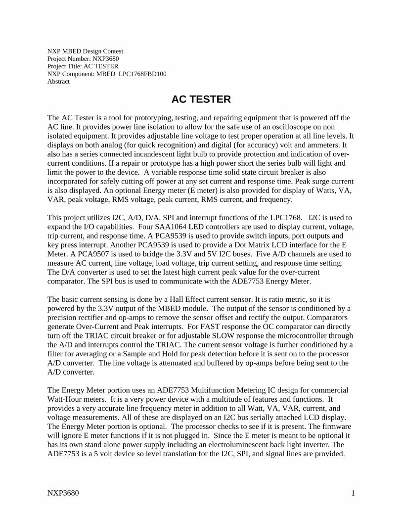
NXP MBED Design Contest Project Number: NXP3680 Project Title: AC TESTER NXP Component: MBED LPC1768FBD100 Abstract
AC TESTER
The AC Tester is a tool for prototyping, testing, and repairing equipment that is powered off the AC line. It provides power line isolation to allow for the safe use of an oscilloscope on non isolated equipment. It provides adjustable line voltage to test proper operation at all line levels. It displays on both analog (for quick recognition) and digital (for accuracy) volt and ammeters. It also has a series connected incandescent light bulb to provide protection and indication of over-current conditions. If a repair or prototype has a high power short the series bulb will light and limit the power to the device. A variable response time solid state circuit breaker is also incorporated for safely cutting off power at any set current and response time. Peak surge current is also displayed. An optional Energy meter (E meter) is also provided for display of Watts, VA, VAR, peak voltage, RMS voltage, peak current, RMS current, and frequency. This project utilizes I2C, A/D, D/A, SPI and interrupt functions of the LPC1768. I2C is used to expand the I/O capabilities. Four SAA1064 LED controllers are used to display current, voltage, trip current, and response time. A PCA9539 is used to provide switch inputs, port outputs and key press interrupt. Another PCA9539 is used to provide a Dot Matrix LCD interface for the E Meter. A PCA9507 is used to bridge the 3.3V and 5V I2C buses. Five A/D channels are used to measure AC current, line voltage, load voltage, trip current setting, and response time setting. The D/A converter is used to set the latest high current peak value for the over-current comparator. The SPI bus is used to communicate with the ADE7753 Energy Meter. The basic current sensing is done by a Hall Effect current sensor. It is ratio metric, so it is powered by the 3.3V output of the MBED module. The output of the sensor is conditioned by a precision rectifier and op-amps to remove the sensor offset and rectify the output. Comparators generate Over-Current and Peak interrupts. For FAST response the OC comparator can directly turn off the TRIAC circuit breaker or for adjustable SLOW response the microcontroller through the A/D and interrupts control the TRIAC. The current sensor voltage is further conditioned by a filter for averaging or a Sample and Hold for peak detection before it is sent on to the processor A/D converter. The line voltage is attenuated and buffered by op-amps before being sent to the A/D converter. The Energy Meter portion uses an ADE7753 Multifunction Metering IC design for commercial Watt-Hour meters. It is a very power device with a multitude of features and functions. It provides a very accurate line frequency meter in addition to all Watt, VA, VAR, current, and voltage measurements. All of these are displayed on an I2C bus serially attached LCD display. The Energy Meter portion is optional. The processor checks to see if it is present. The firmware will ignore E meter functions if it is not plugged in. Since the E meter is meant to be optional it has its own stand alone power supply including an electroluminescent back light inverter. The ADE7753 is a 5 volt device so level translation for the I2C, SPI, and signal lines are provided.

NXP3680 2
NXP3680 3
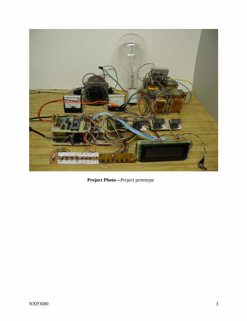
Project Photo—Project prototype
NXP3680 4
VARIAC
MBED
METERENERGY
BREAKERCIRCUIT
ELECTRONICTRANSFORMERISOLATION
TRIP
DISPLAYDISPLAY
DISPLAYVOLTAGE
DISPLAYCURRENT
LCD DISPLAY
CURRENT TIMERESPONSE
1 2
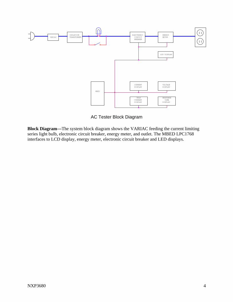
AC Tester Block Diagram Block Diagram—The system block diagram shows the VARIAC feeding the current limiting series light bulb, electronic circuit breaker, energy meter, and outlet. The MBED LPC1768 interfaces to LCD display, energy meter, electronic circuit breaker and LED displays.
NXP3680 5
VLOAD
34
5
68
712
LS1
RELAY DPDT
LINE
ISO_NEUT
D31N4001
Q12N7002
R447K
TO E METER
R2680/.5W
L1VARIAC
12
3J2PLUG AC MALE
SW5SW DPDT
SW2
SW DPDT
R1820/.5W
SW1
10A SW/BRKR
14
23
T1
600VA
14
23
T3
600VA
14
23
T2
600VA
1 2
DS1300W
14
23
T4
600VA
SW3
SW6
SW SPDTRV2
V25S150P
NORMAL
BOOST
BYPASS 110V
SW4
220V
1 2
DS21000W
12
3
J3PLUG AC FEMALE
12
3
J4PLUG AC FEMALE
RV1V25S150P
+12V
TOECB
FRMECB
1234567
J1
HIRNG
HI RANGE
1 2V
M2 150/300VAC
1 2AM1
10A AC
NEUT
R36.80K/2W
C1.47UF/400V
1
2
6
54
3
7
8U1 TLP222
D21N4007
D4LED
D1LED
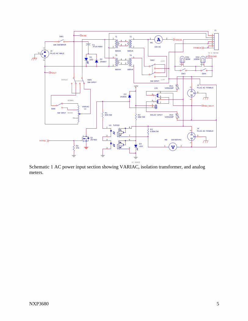
Schematic 1 AC power input section showing VARIAC, isolation transformer, and analog meters.
NXP3680 6
D51N4148
C9.1UF
5
8 9
7
6
35 6
R9
10K
RESET#
SW8
SW SPDT
INTOC#
TRIPPED#
TRIPPED
ONSW7
Q52N7000
Q42N7000
Q32N7000
R1147K
R1247K
R1347K
OFF
+3.3V
+3.3VOUT
IP1+1
IP2+2
IP3+3
IP4+4
IP1-5
IP2-6
IP3-7
IP4-8
FAULT_EN16
VOC15
VC
C14
FAULT13
VIOUT12
FILTER11
VZCR10
GN
D9
U2
ACS710-12
FLTR1
SLOW
FAST
FLTR2 FLTR3
Q62N7002
L3
1 UHY
L2
1 UHY
1
23
14
7
U4A74HC00
1
23
U5A 74HC00
C4.001UF
C5.001UF
C6.01UF
C7.1UF
FRMECB
C81UF
VCZR
C2.1UF
C3.01UF/400V
R5 56/2W
R8 82
R7 390R6390
Q2BTA225-800
1
2
6
4
CIRCUITCROSSZERO
U3
MOC3063
TOECB
+3.3V
ISENSE
VSENSE
PWRON#
D6LED
R1082
+3.3V
TRIPPED
TRIPPED#
RESP
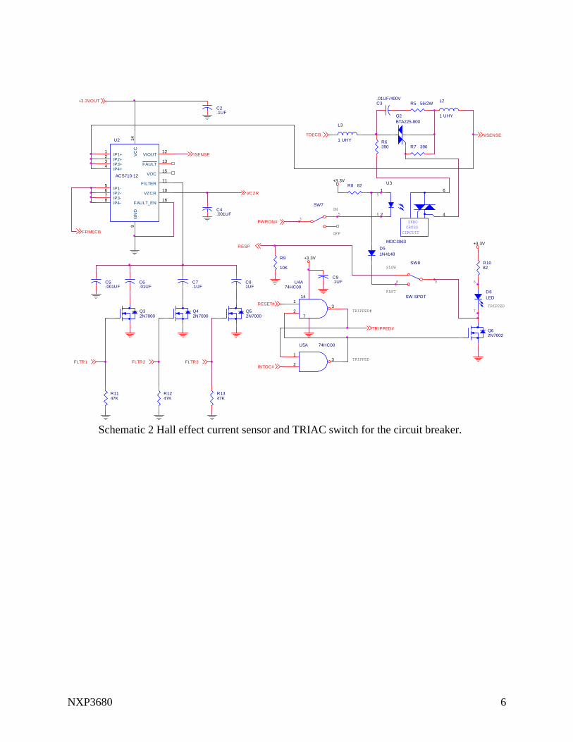
Schematic 2 Hall effect current sensor and TRIAC switch for the circuit breaker.
NXP3680 7
+5VA
R15
10.0K
R19
10.0K
R14
10.0K
R20 10K
+3.3V
R21 10K
R27 10K
R28 10K
D7
1N4148
+5VA
C11.1UF
C10.1UF
+5VA
AIN
ISENSE
R183.3K
R263.3K
+5VA
-5VA
R25 20.0K
R2210.0K
R29 10.0K
9
814
312
-
+
U7C
LM339A
+3.3V
11
1013
312
-
+
U7D
LM339A
+3.3V
C14.1UF
R171K
+ C1310UF
OC SET
3
21
84
-
+
U8ALM358A
#INTOC
-5VA
#INTPEAK
ADOCSET
C12.1UF
AOUT
VCZR
R2420.0K
2
31
411
-
+
U6A
LM324
R16 330K
R23 330K
6
57
+
-
U6B
LM324
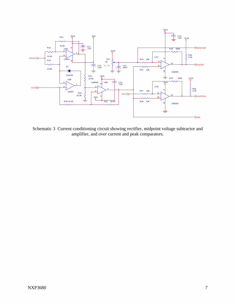
Schematic 3 Current conditioning circuit showing rectifier, midpoint voltage subtractor and amplifier, and over current and peak comparators.
NXP3680 8
INH6
VEE7 VDD
16
X14
X012
X113
Y15
Y02
Y11
Z4
Z05
Z13
A11
B10
C9
U10
4053
APSEL
R304.7K
IADC
C15.1UF
+5VA
R311M
+5V
RC14
CX15
A112
A011
Q10Q9
VDD16
RST13
U41B
4538
-5V
POLY
20 uS
0=AVG
POLY
1=PK
D8 1N4148
-5VA
C18.1UF
AIN
C16.1UF
AIN3
AOUT5
CAP6
VC
C1
VE
E4
GN
D7
SAMPLE8
U11
LF398
#INTPEAK
R3210K
C21.0022UF
C20.1UF C22
.1UF
C19.01UF
C17.1UF
D9
1N4148
+5VA
+5V-5VA
3
21
84
-
+
U9A
LM358A
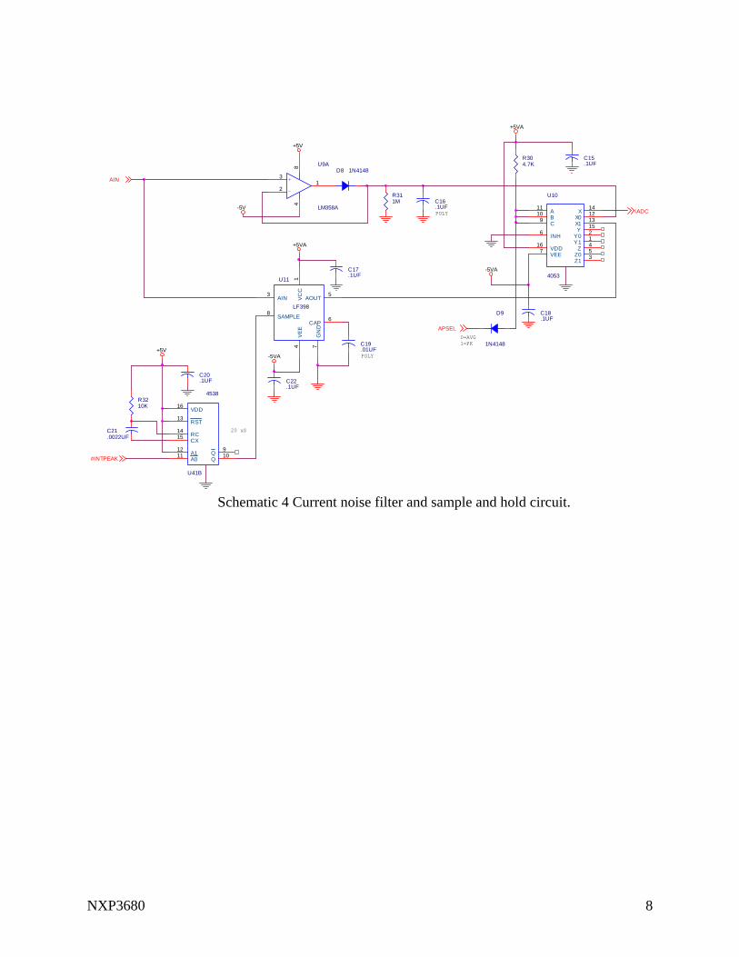
Schematic 4 Current noise filter and sample and hold circuit.
NXP3680 9
D12 1N4007
D15 1N4007
C231UF/400V
C251UF/400V
C24.1UF
C26.1UF
+3.3V
9
108
-
+
U6C
LM324
R35
1.0M
R34
1.0M
13
1214
+
-
U6D
LM324
R41
1.0M
R40
1.0M
R39
1.0M
R3733.2K
R33
1.0M
121:1 ATTN
R38
1.0M
FAULT
VSENSE
D111N4148
D131N4148
D141N4148
D161N4148
+3.3V
R4233.2K
VLOAD
D103.6V TVS
F1 1/2A
R43 220K DS3 NE-2H
ISO_NEUT
R36
1.0M
ADVLOAD
ADVAC
+3.3V
R441K
+ C2710UF
ADRESPTIME
TIMERESPONSE
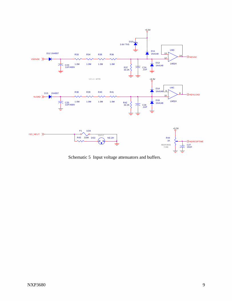
Schematic 5 Input voltage attenuators and buffers.
NXP3680 10
SWIRQ#
MEIRQ#
INTZCROSSI#
INTZCROSSV#
TRIPPED#
HIRNG
PWRON#
BEEPER
MERESET#
+5VA
MECS#
#INTPEAK
#INTOC
EMISO
ADVAC
ADOCSET
ADRESPTIME
ADVLOAD
IADC
SDA1
SCL1
EMOSI
ESCK
AOUT
+3.3VOUT
MESAG#
MEZX
MECF
GND1
VIN2
VBAT3
NRES4
P0.9/I2STXSDA/MOSI1/MAT2.35
P0.8/I2STXWS/MISO1/MAT2.26
P0.7/I2STXCLK/SCK1/MAT2.17
P0.6/I2SRXSDA/SSEL1/MAT2.08
P0.0/CANRX1/TXD3/SDA19
P0.1/CANTX1/RXD3/SCL110
P0.18/DCD1/MOSI0/MOSI111
P0.17/CTS1/MISO0/MISO12
P0.15/TXD1/SCK0/SCK13
P0.16/RXD1/SSEL0/SSEL14
P0.23/AD0.0/I2SRXCLK/CAP3.015
P0.24/AD0.1/ISRXWS/CAP3/.116
P0.25/AD0.2/I2SRXSDA/TXD317
P0.26/AD0.3/AOUT/RXD318
P1.30/VBUS/AD0.419
P1.31/SCK1/AD0.520
DTR1/PWM1.6/P2.521
DSR1/PWM1.5/P2.422
DCD1/PWM1.4/P2.323
CTS1/PWM1.3/P2.224
RXD1/PWM1.2/P2.125
RXD1/PWM1.1/P2.026
MAT3.1/SCL2/RXD2/P0.1127
MAT3.0/SDA2/TXD2/P0.1028
CAP2.1/CANTX2/I2SRXWS/P0.529
CAP2.0/CANRX2/I2SRXCLK/P0.430
USBD+31
USBD-32
TXD+33
TXD-34
RXD+35
RXD-36
IF+37
IF-38
5VOUT39
3.3VOUT40
U13
mbed_LPC1768
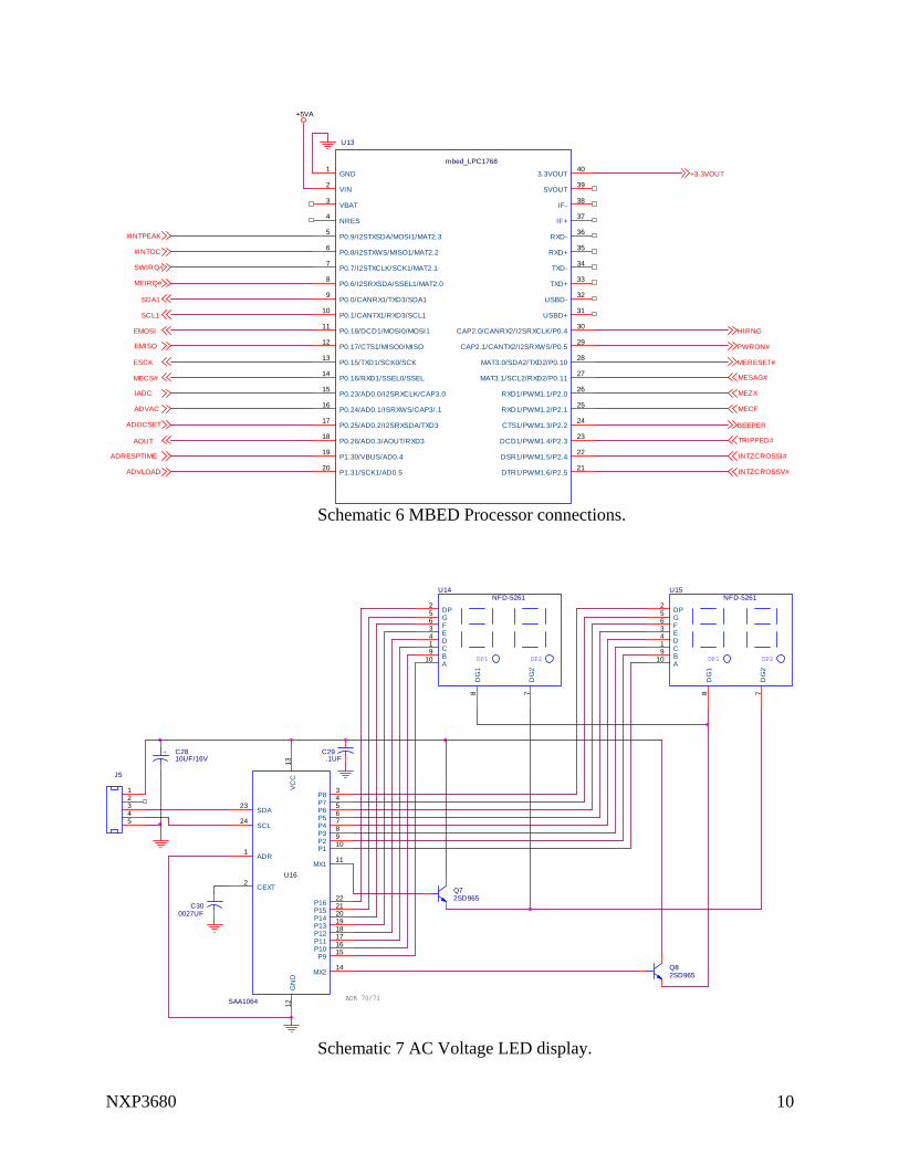
Schematic 6 MBED Processor connections.
12345
J5
C29.1UF
A10 B9 C1 D4 E3 F6 G5 DP2
DG
18
DG
27
DP1 DP2
U14NFD-5261
A10 B9 C1 D4 E3 F6 G5 DP2
DG
18
DG
27
DP1 DP2
U15NFD-5261
C30.0027UF
ADR 70/71
+ C2810UF/16V
P110P29P38P47P56P65P74P83
P915P1016P1117P1218P1319P1420P1521P1622
SDA23
SCL24
MX214
MX111
GN
D12
VC
C13
ADR1
CEXT2
U16
SAA1064
Q72SD965
Q82SD965
Schematic 7 AC Voltage LED display.
NXP3680 11
I2C IN
C32.1UF
A10 B9 C1 D4 E3 F6 G5 DP2
DG
18
DG
27
DP1 DP2
U17NFD-5261
A10 B9 C1 D4 E3 F6 G5 DP2
DG
18
DG
27
DP1 DP2
U18NFD-5261
C33.0027UF
ADR 72/73
12345
J6
Q92SD965
Q102SD965
+ C3110UF/16V
P110P29P38P47P56P65P74P83
P915P1016P1117P1218P1319P1420P1521P1622
SDA23
SCL24
MX214
MX111
GN
D1
2V
CC
13
ADR1
CEXT2
U19
SAA1064
R461.8K
R453.3K
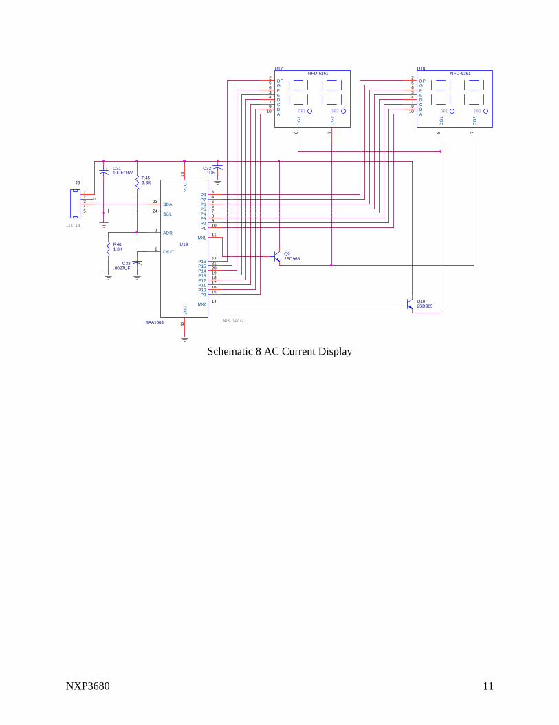
Schematic 8 AC Current Display
NXP3680 12
Q112SD965
Q122SD965
C36.0027UF
ADR 74/75
P110P29P38P47P56P65P74P83
P915P1016P1117P1218P1319P1420P1521P1622
SDA23
SCL24
MX214
MX111
GN
D12
VC
C13
ADR1
CEXT2
U22
SAA1064
R483.3K
R471.8K
12345
J7
+ C3410UF/16V
C35.1UF
A10 B9 C1 D4 E3 F6 G5 DP2
DG
18
DG
27
DP1 DP2
U20NFD-5261
A10 B9 C1 D4 E3 F6 G5 DP2
DG
18
DG
27
DP1 DP2
U21NFD-5261
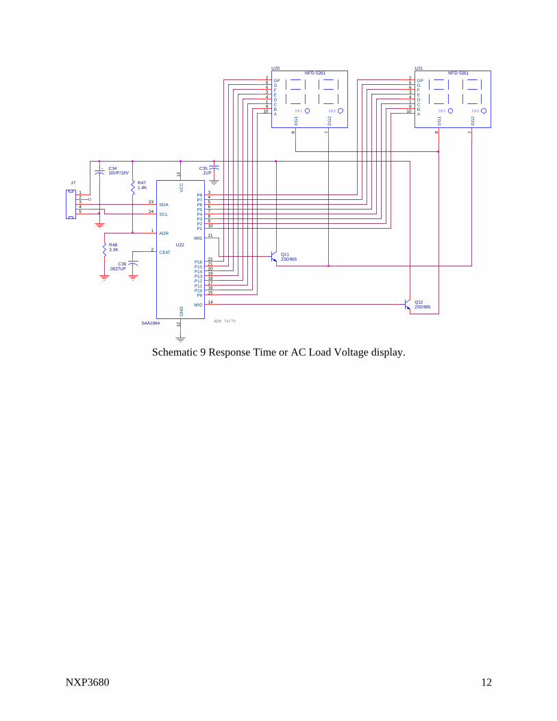
Schematic 9 Response Time or AC Load Voltage display.
NXP3680 13
Q14
Q132SD965
2SD965
C39.0027UF
ADR 76/77
P110P29P38P47P56P65P74P83
P915P1016P1117P1218P1319P1420P1521P1622
SDA23
SCL24
MX214
MX111
GN
D12
VC
C13
ADR1
CEXT2
U25
SAA1064
C38.1UF
A10 B9 C1 D4 E3 F6 G5 DP2
DG
18
DG
27
DP1 DP2
U23NFD-5261
A10 B9 C1 D4 E3 F6 G5 DP2
DG
18
DG
27
DP1 DP2
U24NFD-5261
12345
J8
+ C3710UF/16V
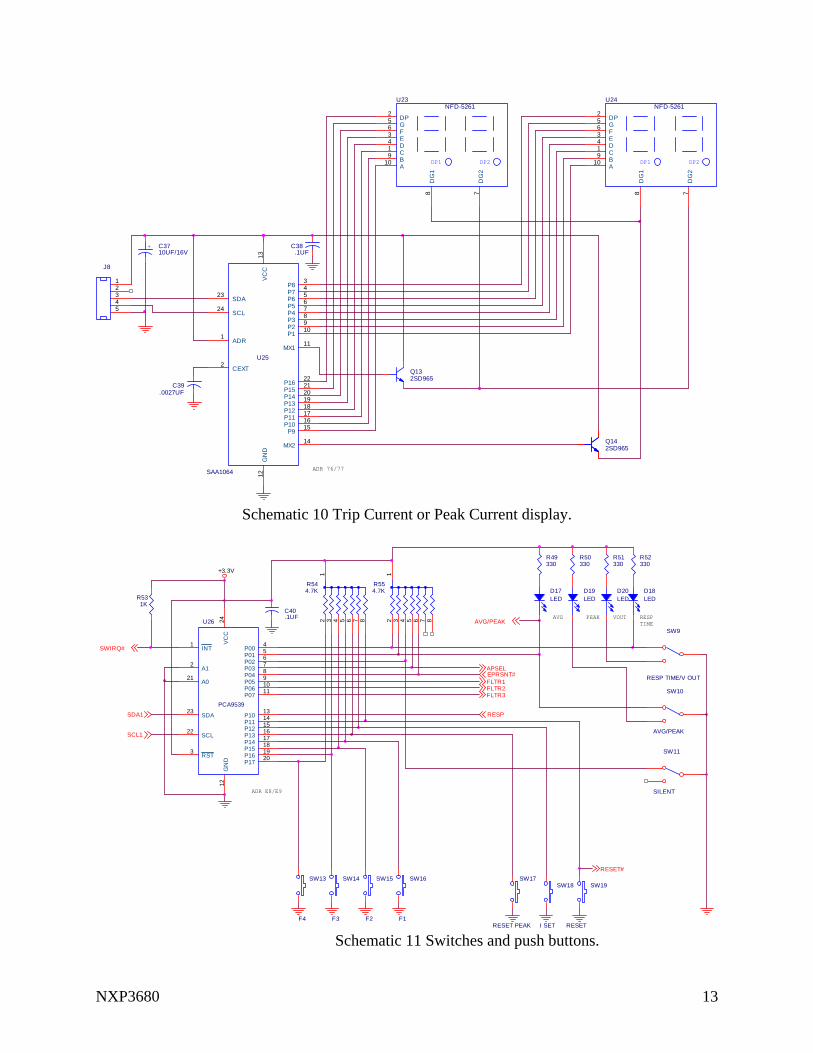
Schematic 10 Trip Current or Peak Current display.
P004
P015
P026
P037
P048
P059
P0610
P0711
P1013
P1114
P1215
P1316
P1417
P1518
P1619
P1720
INT1
A021
A12
RST3
SDA23
SCL22
GN
D12
VC
C24U26
PCA9539
FLTR1
SW15
F2
SW16
F1
SW18
I SET
FLTR2
SW19
RESET
FLTR3
RESET#
R531K
SW17
RESET PEAK
R49330
C40.1UF
R50330
+3.3V
R51330
R52330
D17LED
D19LED
12 3 4 5 6 7 8
R544.7K D20
LEDD18LED
12 3 4 5 6 7 8
R554.7K
AVG/PEAK
RESPSDA1
SCL1
SWIRQ#
EPRSNT#
ADR E8/E9
APSEL
SW14
F3
SW13
F4
SW11
AVG/PEAK
SW10
SILENT
SW9
RESP TIME/V OUT
VOUTTIMERESPPEAKAVG
Schematic 11 Switches and push buttons.
NXP3680 14
ACV
IADC
INTZCROSSV#
INTZCROSSI#
SDA5V
SCL5V
R603.3K
R61 1M
R66 1M
R64 1M
R70 1M
-5VA
TO E METER+3.3V
R581K
R591K
R57680
R56680
C42.1UF
C41.1UF
+5V
VC
CA
1
SCLA2
SDAA3
GN
D4
EN5
SDAB6
SCLB7
VC
CB
8 U27
PCA9507
+3.3V
SCL1
SDA112345
J10
7
61
312
-
+
U7A
LM339
5
42
312
-
+
U7B
LM339
R6510K
R6910K
R623.3K
R673.3K
R63 10K
R68 10K
+5VA
+5VA
13579
111315
246810121416
J9
+3.3V
EMOSIESCK
MEREST#MECS#
+3.3V
EPRSNT#
MEIRQ#
EMISO
MEZXMESAG#
MECF
+3.3V
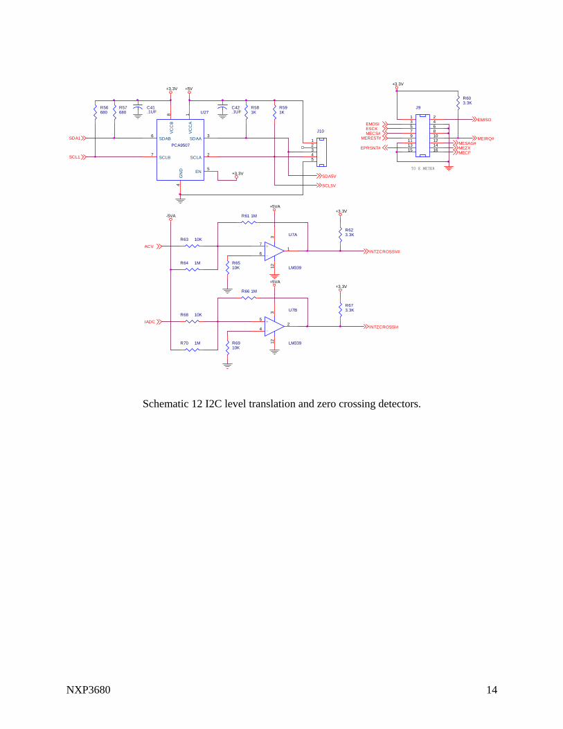
Schematic 12 I2C level translation and zero crossing detectors.
NXP3680 15
COMMON POINT GROUND
ACV
VCC6
CO
LD
RV
8
SW
CO
L1
ISE
N7
GN
D4
CT
3
SW2
CO
MP
IN5
U29
MC34063
+ C50100UF/16V
+ C54100UF/16V
R71.075/2W
8
76
5
4
32
1T5
DST-7-16
R741.2K
R72330/1W
R733.6K
C46560PF
L4
100UHY
LINE
D22SB540 + C44
100UF/16V
D23P1.5KE6.8
NEUT
Q1627P06
C43.1UF
D
S
G
+ C511500UF/25V
+ C55330UF/25V
IN2
OUT3
GN
D1
U32 79L05
IN1
OUT3
GN
D2
U30
78M05
GN
D1
OUT2
IN3
U31
78M33
C49.1UF
C53.1UF
C57.1UF
C56.1UF
D25 1N5402
+12V
C48.1UF
C52.1UF
D29 1N4002
D271N4002
+ C474700UF/25V
D281N4002
D26 1N4002
D30 1N5402
+ C45
2200UF/25V
D2115V
+5V
+5VA
+ C58100UF/16V
+3.3V
D24 1N4002
-5VA
D31 1N4002
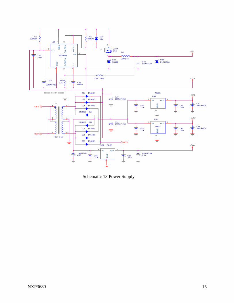
Schematic 13 Power Supply
NXP3680 16
SDA5V
SCL5V
+ C59470UF/25V
+ C61100UF/16V
D321N4002
BEEPER
R7747K
Q182N7000
LS2
BEEPER
+5V
SDA1
SCL2
OS3
GN
D4
A25
A16
A07
VD
D8U33
LM75
Q17TIP30
R75100
R761K
+5V
+12V
C60.1UF
12
J11
CON2
THERMALLY ATTACH TO TRIAC HEATSINK
FAN
ADR 0x90
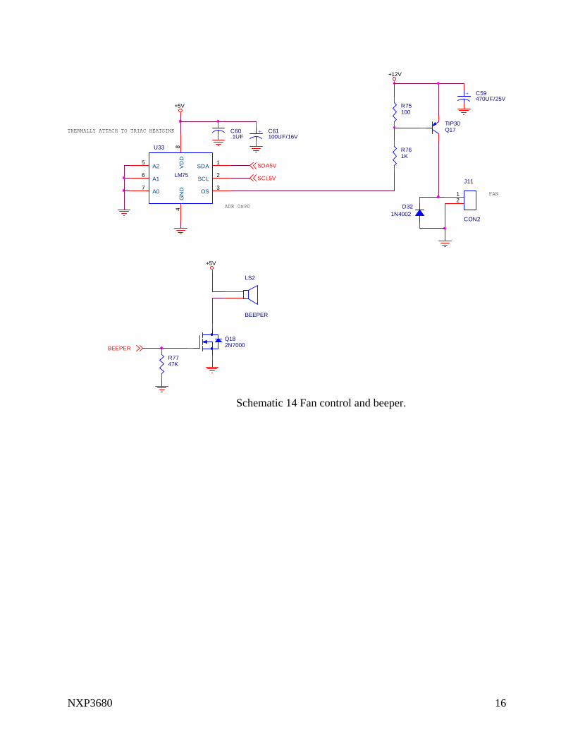
Schematic 14 Fan control and beeper.
NXP3680 17
FROM CTRLR
13579
111315
246810121416
J12
+3.3V
B to AA to B
A13 A24 A35 A46 A57 A68 A79 A8
10
B121B220B319B418B517B616B715B814
GN
D1
11
GN
D2
12
GN
D3
13
VC
CA
1
VC
CB
124
VC
CB
223
DIR2
OE22
U34
74LVC4245
A13 A24 A35 A46 A57 A68 A79 A8
10
B121B220B319B418B517B616B715B814
GN
D1
11
GN
D2
12
GN
D3
13
VC
CA
1
VC
CB
124
VC
CB
223
DIR2
OE22
U35
74LVC4245
C63.1UF
C62.1UF
C64.1UF
C65.1UF
+5V+5V
EDIN
ECS#ESCLK
ERESET#
EDOUTEIRQ#ESAG#EZXECF
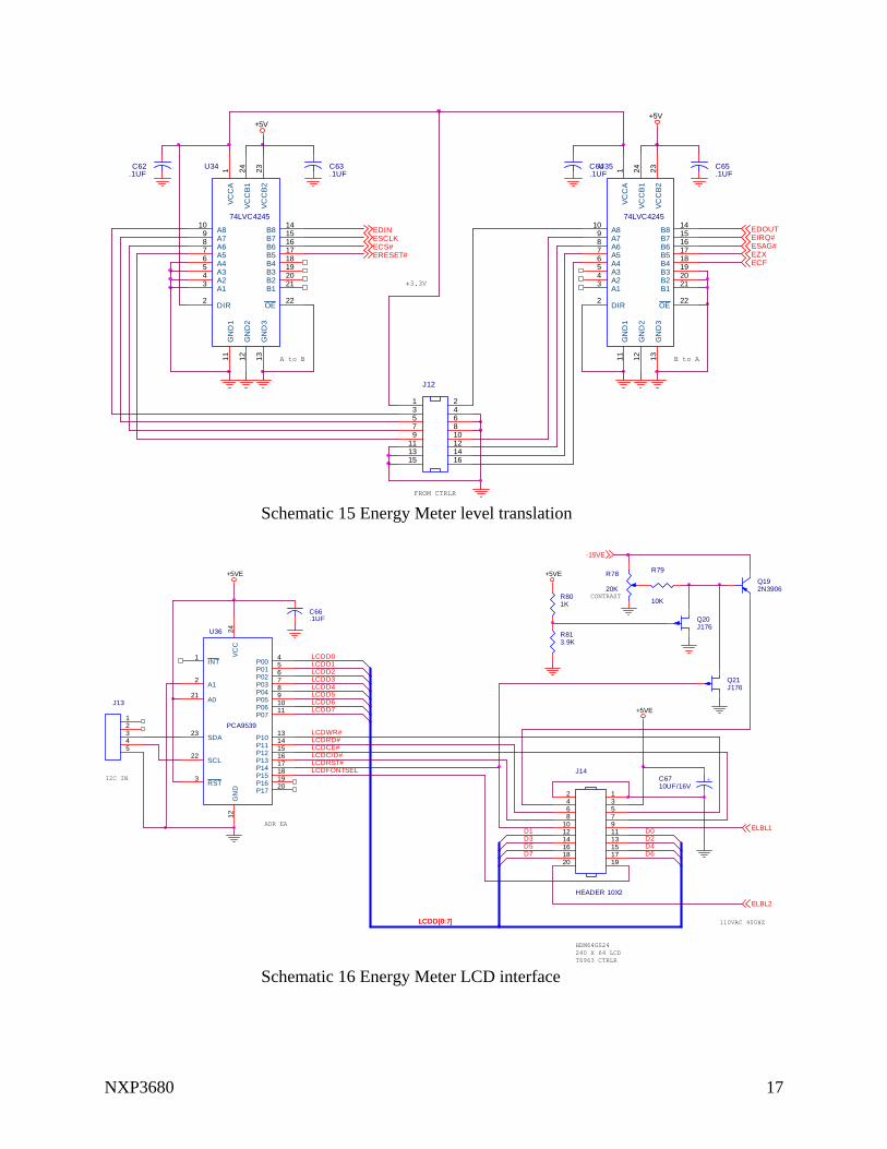
Schematic 15 Energy Meter level translation
I2C IN
LCDWR#
C66.1UF
+5VE
P004
P015
P026
P037
P048
P059
P0610
P0711
P1013
P1114
P1215
P1316
P1417
P1518
P1619
P1720
INT1
A021
A12
RST3
SDA23
SCL22
GN
D12
VC
C2
4
U36
PCA9539
135791113151719
2468
101214161820
J14
HEADER 10X2
D4D2D0D1
D6
+5VE
D5D3
D7
LCDD[0:7]LCDD[0:7]
R801K
+5VE
+C6710UF/16V
ELBL2
ELBL1
240 X 64 LCDHDM64GS24
110VAC 400HZ
T6963 CTRLR
Q192N3906
R78
20K
-15VE
R79
10K
Q20J176
R813.9K
LCDCE#
ADR EA
CONTRAST
LCDRD#
LCDC/D#
12345
J13
LCDRST#LCDFONTSEL
LCDD0LCDD1
Q21J176
LCDD3LCDD2
LCDD6LCDD5LCDD4
LCDD7
Schematic 16 Energy Meter LCD interface
NXP3680 18
AC IN
CURRENT XFMR
E110VLNE110VNT
V1P4
V1N5
V2P7
V2N6
RESET1
DV
DD
2
AV
DD
3A
GN
D8
REF9
DG
ND
10
CF11
ZX12
SAG13
IRQ14CLKIN
15
CLKOUT16
CS17
SCLK18
DOUT19
DIN20
U37
ADE7753
C70.1UF
1234567
J15
CON7
C69.1UF
C68.033UF
C72.033UF
C74.033UFC75.033UF
C7622PF
C7722PF
C781UF
Y13.579Mhz
EDOUT
EZX
EIRQ#
ECF
ESAG#
ESCLK
ECS#
EDIN
+ C7110UF
+
C7310UF
R83 1.0K
R85 1.0K
R8211.3
R8411.3
R881.0K
R89
1.0K
R87
499K
R86
499K
ERESET#
+5VEL5
BEAD
2
5
1
4
6
3
T6
CS2106
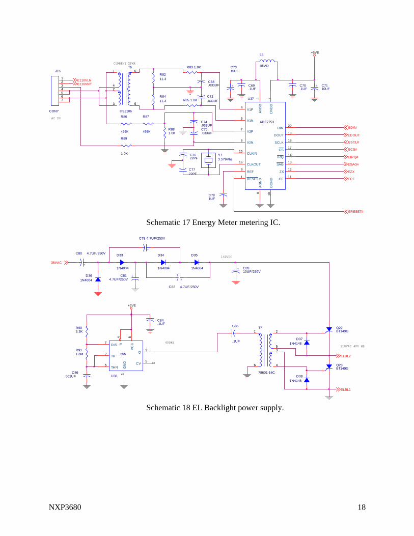
Schematic 17 Energy Meter metering IC.
C84.1UF
+5VE
110VAC 400 HZ
160VDC
400HZ
ELBL2
ELBL1
+ C8310UF/250V
36VAC
D361N4004
D33
1N4004
D34
1N4004
D35
1N4004
+
C80 4.7UF/250V
+C814.7UF/250V
+
C79 4.7UF/250V
+
C82 4.7UF/250V
C85
.1UF
TR2
CV5
Q3
DIS7
THR6
R4
VC
C8
GN
D1
U38
555
Q22BT149G
Q23BT149G
R903.3K
R911.8M
C86.001UF
3
6
2
5
1
4
T7
78601-16C
D371N4148
D381N4148
Schematic 18 EL Backlight power supply.
NXP3680 19
+5VE
-15VE
36VAC
IN2
OUT3
GN
D1
U40
79L15
C88.1UF
C89.1UF
C93.1UF
C92.1UF
IN1
OUT3
GN
D2
U3978M05
+
C87220UF/50V
+C9122UF/50V
D39
1N4002
D40
1N4002
8
76
5
4
32
1T8
DST-3-36
E110VLN
E110VNT
+ C9010UF/25V
+ C9410UF/25V
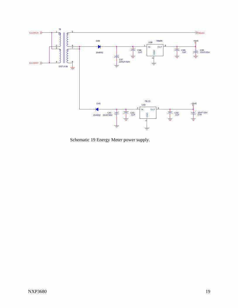
Schematic 19 Energy Meter power supply.
NXP3680 20
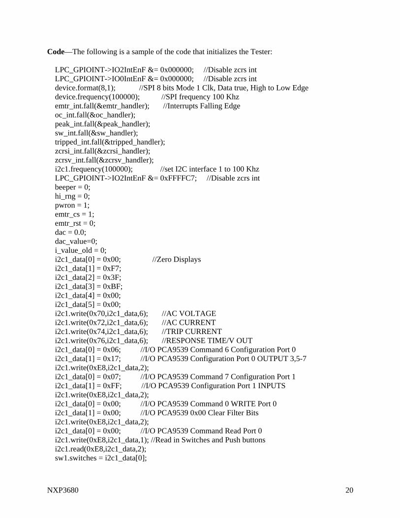
Code—The following is a sample of the code that initializes the Tester: LPC_GPIOINT->IO2IntEnF &= 0x000000; //Disable zcrs int LPC_GPIOINT->IO0IntEnF &= 0x000000; //Disable zcrs int device.format(8,1); //SPI 8 bits Mode 1 Clk, Data true, High to Low Edge device.frequency(100000); //SPI frequency 100 Khz emtr_int.fall(&emtr_handler); //Interrupts Falling Edge oc_int.fall(&oc_handler); peak_int.fall(&peak_handler); sw_int.fall(&sw_handler); tripped_int.fall(&tripped_handler); zcrsi_int.fall(&zcrsi_handler); zcrsv_int.fall(&zcrsv_handler); i2c1.frequency(100000); //set I2C interface 1 to 100 Khz LPC_GPIOINT->IO2IntEnF &= 0xFFFFC7; //Disable zcrs int beeper = 0; hi_rng = 0; pwron = 1; emtr_cs = 1; emtr_rst = 0; dac = 0.0; dac_value=0; i_value_old = 0; i2c1_data[0] = 0x00; //Zero Displays i2c1_data[1] = 0xF7; i2c1_data[2] = 0x3F; i2c1_data[3] = 0xBF; i2c1_data[4] = 0x00; i2c1_data[5] = 0x00; i2c1.write(0x70,i2c1_data,6); //AC VOLTAGE i2c1.write(0x72,i2c1_data,6); //AC CURRENT i2c1.write(0x74,i2c1_data,6); //TRIP CURRENT i2c1.write(0x76,i2c1_data,6); //RESPONSE TIME/V OUT i2c1_data[0] = 0x06; //I/O PCA9539 Command 6 Configuration Port 0 i2c1_data[1] = 0x17; //I/O PCA9539 Configuration Port 0 OUTPUT 3,5-7 i2c1.write(0xE8,i2c1_data,2); i2c1_data[0] = 0x07; //I/O PCA9539 Command 7 Configuration Port 1 i2c1_data[1] = 0xFF; //I/O PCA9539 Configuration Port 1 INPUTS i2c1.write(0xE8,i2c1_data,2); i2c1_data[0] = 0x00; //I/O PCA9539 Command 0 WRITE Port 0 i2c1_data[1] = 0x00; //I/O PCA9539 0x00 Clear Filter Bits i2c1.write(0xE8,i2c1_data,2); i2c1_data[0] = 0x00; //I/O PCA9539 Command Read Port 0 i2c1.write(0xE8,i2c1_data,1); //Read in Switches and Push buttons i2c1.read(0xE8,i2c1_data,2); sw1.switches = i2c1_data[0];
NXP3680 21
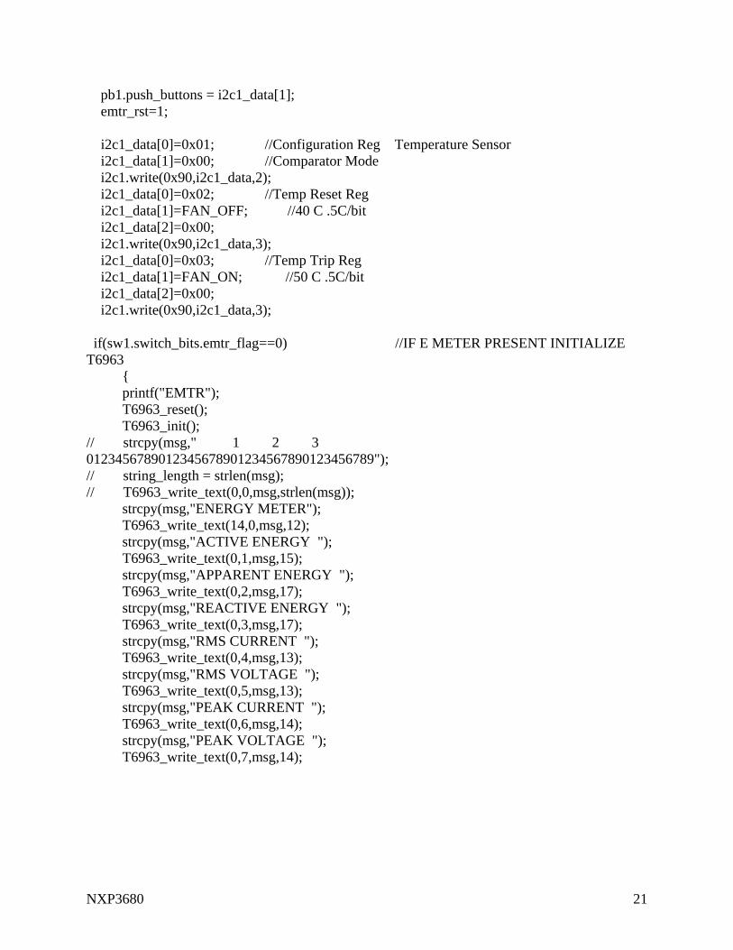
pb1.push_buttons = i2c1_data[1]; emtr_rst=1; i2c1_data[0]=0x01; //Configuration Reg Temperature Sensor i2c1_data[1]=0x00; //Comparator Mode i2c1.write(0x90,i2c1_data,2); i2c1_data[0]=0x02; //Temp Reset Reg i2c1_data[1]=FAN_OFF; //40 C .5C/bit i2c1_data[2]=0x00; i2c1.write(0x90,i2c1_data,3); i2c1_data[0]=0x03; //Temp Trip Reg i2c1_data[1]=FAN_ON; //50 C .5C/bit i2c1_data[2]=0x00; i2c1.write(0x90,i2c1_data,3); if(sw1.switch_bits.emtr_flag==0) //IF E METER PRESENT INITIALIZE T6963 { printf("EMTR"); T6963_reset(); T6963_init(); // strcpy(msg," 1 2 3 0123456789012345678901234567890123456789"); // string_length = strlen(msg); // T6963_write_text(0,0,msg,strlen(msg)); strcpy(msg,"ENERGY METER"); T6963_write_text(14,0,msg,12); strcpy(msg,"ACTIVE ENERGY "); T6963_write_text(0,1,msg,15); strcpy(msg,"APPARENT ENERGY "); T6963_write_text(0,2,msg,17); strcpy(msg,"REACTIVE ENERGY "); T6963_write_text(0,3,msg,17); strcpy(msg,"RMS CURRENT "); T6963_write_text(0,4,msg,13); strcpy(msg,"RMS VOLTAGE "); T6963_write_text(0,5,msg,13); strcpy(msg,"PEAK CURRENT "); T6963_write_text(0,6,msg,14); strcpy(msg,"PEAK VOLTAGE "); T6963_write_text(0,7,msg,14);

NXP3680 22