Embed Size (px)
Citation preview

ACEPACK™ 1
Features• ACEPACK™ 1 power module
– DBC Cu Al2O3 Cu• Sixpack topology
– 650 V, 50 A IGBTs and diodes– Soft and fast recovery diode
• Integrated NTC
Applications• Inverters• Industrial• Motor drives
DescriptionThis power module is a sixpack topology in an ACEPACK™ 1 package with NTC,integrating the advanced trench gate field-stop technology from STMicroelectronics.This new IGBT technology represents the best compromise between conduction andswitching loss, to maximize the efficiency of any converter system up to 20 kHz.
Product status
A1P50S65M2
Product summary
Order code A1P50S65M2
Marking A1P50S65M2
Package ACEPACK™ 1
Leads type Solder contact pins
ACEPACK™ 1 sixpack topology, 650 V, 50 A trench gate field-stop IGBT M series, soft diode and NTC
A1P50S65M2
Datasheet
DS12332 - Rev 2 - February 2018For further information contact your local STMicroelectronics sales office.
www.st.com

1 Electrical ratings
1.1 IGBTLimiting values at Tj = 25 °C, unless otherwise specified.
Table 1. Absolute maximum ratings of the IGBT
Symbol Parameter Value Unit
VCES Collector-emitter voltage (VGE = 0) 650 V
IC Continuous collector current (Tc = 100 °C) 50 A
ICP(1) Pulsed collector current (tp = 1 ms) 100 A
VGE Gate-emitter voltage ±20 V
PTOT Total power dissipation of each IGBT (TC = 25 °C, TJ = 175 °C) 208 W
TJMAX Maximum junction temperature 175 °C
TJop Operating junction temperature range under switching conditions -40 to 150 °C
1. Pulse width limited by maximum junction temperature.
Table 2. Electrical characteristics of the IGBT
Symbol Parameter Test conditions Min. Typ. Max. Unit
V(BR)CESCollector-emitterbreakdown voltage IC = 1 mA, VGE = 0 V 650 V
VCE(sat)(terminal)
Collector-emittersaturation voltage
VGE = 15 V, IC= 50 A 1.95 2.3V
VGE = 15 V, IC = 50 A, TJ = 150 ˚C 2.3
VGE(th) Gate threshold voltage VCE = VGE, IC = 1 mA 5 6 7 V
ICES Collector cut-off current VGE = 0 V, VCE = 650 V 100 µA
IGESGate-emitter leakagecurrent VCE = 0 V, VGE = ± 20 V ± 500 nA
Cies Input capacitanceVCE = 25 V, f = 1 MHz,
VGE = 0 V
4150 pF
Coes Output capacitance 170 pF
CresReverse transfercapacitance 80 pF
Qg Total gate chargeVCC = 520 V, IC = 50 A,
VGE = ±15 V150 nC
td(on) Turn-on delay time VCC = 300 V, IC = 50 A,
RG = 6.8 Ω, VGE = ±15 V,
di/dt = 2400 A/µs
143 ns
tr Current rise time 16.5 ns
Eon(1) Turn-on switching energy 0.140 mJ
td(off) Turn-off delay time VCC = 300 V, IC = 50 A,
RG = 6.8 Ω, VGE = ±15 V,
dv/dt = 7600 V/µs
112 ns
tf Current fall time 149 ns
Eoff(2) Turn-off switching energy 1.45 mJ
A1P50S65M2 Electrical ratings
DS12332 - Rev 2 page 2/12

Symbol Parameter Test conditions Min. Typ. Max. Unit
td(on) Turn-on delay time VCC = 300 V, IC = 50 A,
RG = 6.8 Ω, VGE = ±15 V,
di/dt = 2062 A/µs, TJ = 150 °C
148 ns
tr Current rise time 19.2 ns
Eon(1) Turn-on switching energy 0.311 mJ
td(off) Turn-off delay time VCC = 300 V, IC = 50 A,
RG = 6.8 Ω, VGE = ±15 V,
dv/dt = 5800 V/µs, TJ = 150 °C
110 ns
tf Current fall time 221 ns
Eoff(2) Turn-off switching energy 1.98 mJ
tSCShort-circuit withstandtime
VCC ≤ 360 V, VGE ≤ 15 V,
TJstart ≤ 150 °C6 µs
RTHj-cThermal resistancejunction-to-case Each IGBT 0.65 0.72 °C/W
RTHc-hThermal resistance case-to-heatsink Each IGBT, λgrease = 1 W/(m·°C) 0.79 °C/W
1. Including the reverse recovery of the diode.2. Including the tail of the collector current.
1.2 DiodeLimiting values at Tj = 25 °C, unless otherwise specified.
Table 3. Absolute maximum ratings of the diode
Symbol Parameter Value Unit
VRRM Repetitive peak reverse voltage 650 V
IF Continuous forward current at (TC = 100 °C) 50 A
IFP(1) Pulsed forward current (tp = 1 ms) 100 A
TJMAX Maximum junction temperature 175 °C
TJop Operating junction temperature range under switching conditions -40 to 150 °C
1. Pulse width limited by maximum junction temperature.
Table 4. Electrical characteristics of the diode
Symbol Parameter Test conditions Min. Typ. Max. Unit
VF (terminal) Forward voltageIF = 50 A - 1.85 2.65
VIF = 50 A, TJ = 150 ˚C - 1.65
trr Reverse recovery time
IF = 50 A, VR = 300 V,
VGE = ±15 V, di/dt = 2400 A/μs
- 142 ns
Qrr Reverse recovery charge - 1.87 µC
Irrm Reverse recovery current - 40 A
Erec Reverse recovery energy - 0.41 mJ
trr Reverse recovery timeIF = 50 A, VR = 300 V,
VGE = ±15 V, di/dt = 2062 A/μs,
TJ = 150 °C
- 260 ns
Qrr Reverse recovery charge - 5.2 µC
Irrm Reverse recovery current - 58 A
Erec Reverse recovery energy - 1.32 mJ
A1P50S65M2Diode
DS12332 - Rev 2 page 3/12

Symbol Parameter Test conditions Min. Typ. Max. Unit
RTHj-cThermal resistancejunction-to-case Each diode - 1.0 1.1 °C/W
RTHc-hThermal resistance case-to-heatsink Each diode, λgrease = 1 W/(m·°C) - 0.9 °C/W
1.3 NTC
Table 5. NTC temperature sensor, considered as stand-alone
Symbol Parameter Test conditions Min. Typ. Max. Unit
R25 Resistance T = 25°C 5 kΩ
R100 Resistance T = 100°C 493 Ω
ΔR/R Deviation of R100 -5 +5 %
B25/50 B-constant 3375 K
B25/80 B-constant 3411 K
T Operating temperature range -40 150 °C
Figure 1. NTC resistance vs temperature
GADG260720171142NTC
10 4
10 3
10 2 0 25 50 75 100 125
R (Ω)
TC (°C)
Figure 2. NTC resistance vs temperature, zoom
GADG260720171151NTCZ
800
700
600
500
400
30085 90 95 100 105 110
R (Ω)
TC (°C)
max
min
typ
1.4 Package
Table 6. ACEPACK™ 1 package
Symbol Parameter Min. Typ. Max. Unit
Visol Isolation voltage (AC voltage, t = 60 s) 2500 V
Tstg Storage temperature -40 125 °C
CTI Comparative tracking index 200
Ls Stray inductance module P1 - EW loop 28.7 nH
Rs Module single lead resistance, terminal-to-chip 3.9 mΩ
A1P50S65M2NTC
DS12332 - Rev 2 page 4/12

2 Electrical characteristics (curves)
Figure 3. IGBT output characteristics(VGE = 15 V, terminal)
IGBT111020170929TCH
80
60
40
20
00 1 2 3 4
Ic (A)
VCE (V)
TJ = 25 °C
TJ = 150 °C
Figure 4. IGBT output characteristics(TJ = 150 °C, terminal)
IGBT101020171341OC25
90
80
70
60
50
40
30
20
1000 1 2 3 4
IC (A)
VCE (V)
19 V
17 V
15 V
13 V
11 V
VGE = 9 V
Figure 5. IGBT transfer characteristics(VCE = 15 V, terminal)
IGBT101020171339OC25
80
60
40
20
05 6 7 8 9 10 11 12
IC (A)
VGE (V)
TJ = 25 °C
TJ = 150 °C
Figure 6. Switching energy vs gate resistance
IGBT101020171348SLG
4.0
3.0
2.0
1.0
00 20 40 60 80
E (mJ)
RG (Ω)
VCC = 300 V, IC = 50 A, VGE = ±15 V
EON (TJ = 150 °C)
EOFF (TJ = 150 °C)
EOFF (TJ = 25 °C)
EON (TJ = 25 °C)
A1P50S65M2Electrical characteristics (curves)
DS12332 - Rev 2 page 5/12
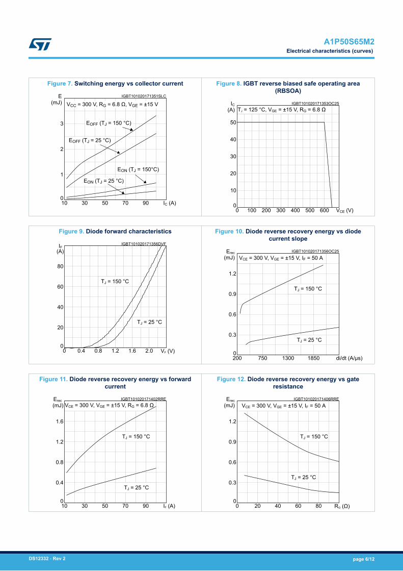
Figure 7. Switching energy vs collector current
IGBT101020171351SLC
3
2
1
010 30 50 70 90
E (mJ)
IC (A)
VCC = 300 V, RG = 6.8 Ω, VGE = ±15 V
EOFF (TJ = 150 °C)
EOFF (TJ = 25 °C)
EON (TJ = 150°C)
EON (TJ = 25 °C)
Figure 8. IGBT reverse biased safe operating area(RBSOA)
IGBT101020171353OC25
50
40
30
20
10
00 100 200 300 400 500 600
IC (A)
VCE (V)
TJ = 125 °C, VGE = ±15 V, RG = 6.8 Ω
Figure 9. Diode forward characteristics
IGBT101020171356DVF
80
60
40
20
00 0.4 0.8 1.2 1.6 2.0 VF (V)
IF(A)
TJ = 150 °C
TJ = 25 °C
Figure 10. Diode reverse recovery energy vs diodecurrent slope
IGBT101020171356OC25
1.2
0.9
0.6
0.3
0200 750 1300 1850
Erec (mJ)
di/dt (A/µs)
VCE = 300 V, VGE = ±15 V, IF = 50 A
TJ = 150 °C
TJ = 25 °C
Figure 11. Diode reverse recovery energy vs forwardcurrent
IGBT101020171402RRE
1.6
1.2
0.8
0.4
010 30 50 70 90
Erec (mJ)
IF (A)
VCE = 300 V, VGE = ±15 V, RG = 6.8 Ω
TJ = 150 °C
TJ = 25 °C
Figure 12. Diode reverse recovery energy vs gateresistance
IGBT101020171406RRE
1.2
0.9
0.6
0.3
00 20 40 60 80
Erec (mJ)
RG (Ω)
VCE = 300 V, VGE = ±15 V, IF = 50 A
TJ = 25 °C
TJ = 150 °C
A1P50S65M2Electrical characteristics (curves)
DS12332 - Rev 2 page 6/12

Figure 13. Inverter diode thermal impedance
IGBT111020170844MT
100
10-1
10-3 10-2 10-1 100
Zth(°C/W)
t (s)
Zth(typ.)JH
Zth(max.)JC
JC
i 1 2 3 4ri (˚C/W) 0.1746 0.5169 0.2851 0.1197
τi(s) 0.0008 0.0074 0.0368 0.2601
JH
iri (˚C/W) 0.2091 0.5735 0.7511 0.3615
τi(s) 0.0010 0.0116 0.0729 0.3310
RC - Foster thermal network
RC - Foster thermal network1 2 3 4
Figure 14. IGBT thermal impedance
IGBT111020170846MT
10 0
10 -1
10 -3 10 -2 10 -1 10 0
Zth (°C/W)
t (s)
JC
i 1 2 3 4ri (˚C/W) 0.0718 0.2858 0.2471 0.1130τi(s) 0.0002 0.0072 0.0392 0.2850
JH
iri (˚C/W) 0.0808 0.3144 0.6701 0.3713τi(s) 0.0003 0.0113 0.0752 0.3492
Zth(typ.)JH
Zth(max.)JC
RC - Foster thermal network
RC - Foster thermal network1 2 3 4
A1P50S65M2Electrical characteristics (curves)
DS12332 - Rev 2 page 7/12

3 Test circuits
Figure 15. Test circuit for inductive load switching
A AC
E
G
B
RG+
-
G
C 3.3 µF
1000 µF
L=100 µH
VCC
E
D.U.T
B
AM015 04v1
Figure 16. Gate charge test circuit
AM01505v1
k
k
k
k
k
k
Figure 17. Switching waveform
AM01506v1
90%
10%
90%
10%
VG
VCE
ICTd(on)
TonTr(Ion)
Td(off)
ToffTf
Tr(Voff)
Tcross
90%
10%
Figure 18. Diode reverse recovery waveform
25
A1P50S65M2Test circuits
DS12332 - Rev 2 page 8/12

4 Topology and pin description
Figure 19. Electrical topology and pin description
P
G1 G3 G5
G2 G4 G6
UV
W
EWE’W
EVE’V
EUE’U
T1
T2
Figure 20. Package top view with sixpack pinout
A1P50S65M2Topology and pin description
DS12332 - Rev 2 page 9/12

5 Package information
In order to meet environmental requirements, ST offers these devices in different grades of ECOPACK®
packages, depending on their level of environmental compliance. ECOPACK® specifications, grade definitionsand product status are available at: www.st.com. ECOPACK® is an ST trademark.
5.1 ACEPACK™ 1 sixpack solder pins package information
Figure 21. ACEPACK™ 1 sixpack solder pins package outline (dimensions are in mm)
33.8±0.3
28.1±0.2
19.4±0.2
16.4±0.2
62.8
±0.
5
53±
0.1
42.5
±0.
2
41±
0.2
48±
0.3
4.5±0.1
3.2 BSC
12±
0.35
15.5
±0.
50
36.8
REF
1.3±0.2
2.5±0.2
3.2
BSC
Detail A
Section B-B
2.3
REF 8.5
3.5 REF x45°
B
B
AA
3.20
6.40
0.00
12.80
16.00
22.40
25.60
28.80
32.00
0.00
6.40
16.0
0
19.2
0
25.6
0
G6
P
W
VW
G5
T1
T2
G3
U
U
G1
E'W EW G4 EV E'V EU E'U
G2
P
V
3.20
9.60
22.4
0
0.64±0.03
GADG240820170900MT_8569715_4
• The lead size includes the thickness of the lead plating material.• Dimensions do not include mold protrusion.• Package dimensions do not include any eventual metal burrs.
A1P50S65M2Package information
DS12332 - Rev 2 page 10/12

Revision history
Table 7. Document revision history
Date Revision Changes
11-Oct-2017 1 Initial release.
16-Feb-2018 2
Updated features and removed maturity status indication from cover page.
Updated Figure 13. Inverter diode thermal impedance and Figure 14. IGBT thermalimpedance.
Updated Figure 21. ACEPACK™ 1 sixpack solder pins package outline(dimensions are in mm).
Minor text changes
A1P50S65M2
DS12332 - Rev 2 page 11/12

IMPORTANT NOTICE – PLEASE READ CAREFULLY
STMicroelectronics NV and its subsidiaries (“ST”) reserve the right to make changes, corrections, enhancements, modifications, and improvements to STproducts and/or to this document at any time without notice. Purchasers should obtain the latest relevant information on ST products before placing orders. STproducts are sold pursuant to ST’s terms and conditions of sale in place at the time of order acknowledgement.
Purchasers are solely responsible for the choice, selection, and use of ST products and ST assumes no liability for application assistance or the design ofPurchasers’ products.
No license, express or implied, to any intellectual property right is granted by ST herein.
Resale of ST products with provisions different from the information set forth herein shall void any warranty granted by ST for such product.
ST and the ST logo are trademarks of ST. All other product or service names are the property of their respective owners.
Information in this document supersedes and replaces information previously supplied in any prior versions of this document.
© 2018 STMicroelectronics – All rights reserved
A1P50S65M2
DS12332 - Rev 2 page 12/12


![Product Overview Sixpack Modules - · PDF fileVII Product Overview Sixpack Modules New I C80 [A] NPT NPT3 Trench IGBT PT IGBT Package 600 V 41 MWI 60 - 06 G6K E1 30 MWI 30 - 06 A7](https://img.pdfslide.net/doc/110x75/5a9dea177f8b9a85318e3fa9/product-overview-sixpack-modules-product-overview-sixpack-modules-new-i-c80-a.jpg)