Embed Size (px)
Citation preview

Achieving Timing Closure
Achieving Timing Closure - 2 © Copyright 2010 Xilinx
Objectives
After completing this module, you will be able to: Describe a flow for obtaining timing closure Interpret a timing report and determine the cause of timing errors Apply Timing Analyzer report options to create customized timing reports

Achieving Timing Closure - 3 © Copyright 2010 Xilinx
Timing Closure

Achieving Timing Closure - 4 © Copyright 2010 Xilinx
Timing Reports
Timing reports help you determine why your design fails to meet its constraints– Reports contain detailed descriptions of paths that fail their constraints
The implementation tools can create timing reports at two points in the design flow– Post-Map Static Timing Report
• Use for an early indication as to whether your design might meet timing
– Post-Place & Route Static Timing Report• Use as a final analysis of whether your design has met timing
The Timing Analyzer is a utility for creating and reading timing reports

Achieving Timing Closure - 5 © Copyright 2010 Xilinx
Double-click Analyze Post-Place & Route Static Timing– Opens the Post-Place & Route Static
Timing Report– Allows you to create custom reports
Open a plain text version by clicking Static Timing Report in the Design Summary screen
Using the Timing Analyzer
Achieving Timing Closure - 6 © Copyright 2010 Xilinx
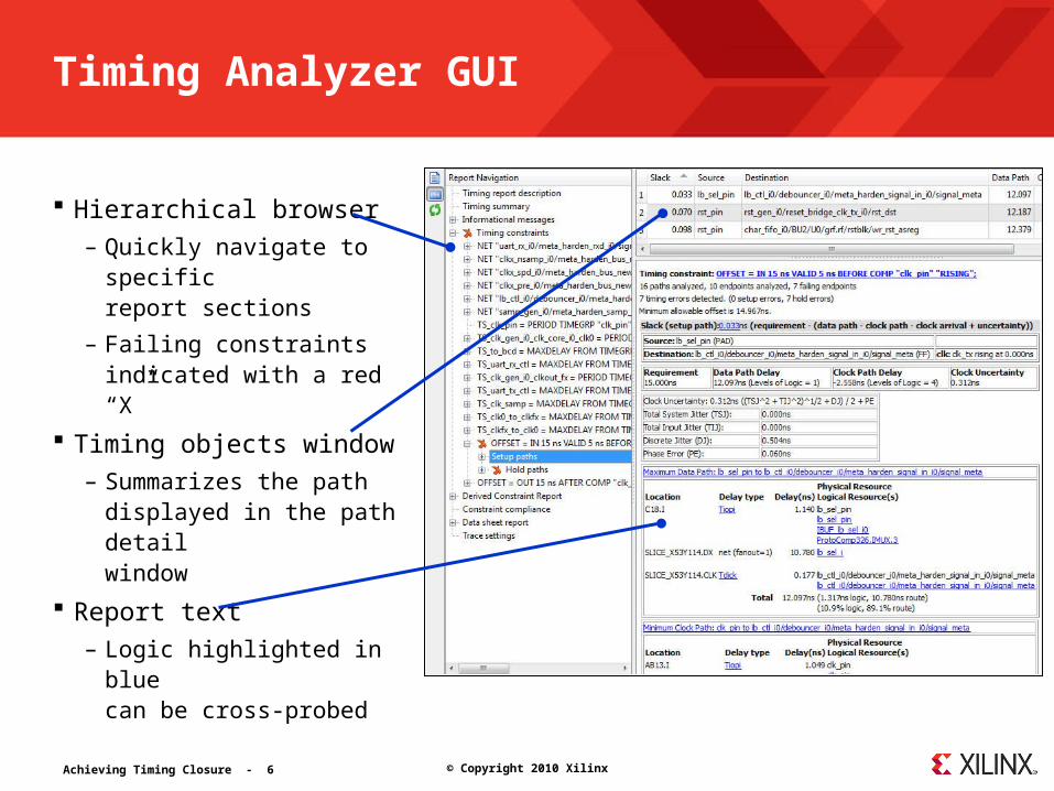
Timing Analyzer GUI
Hierarchical browser– Quickly navigate to specific
report sections– Failing constraints indicated
with a red “X”
Timing objects window– Summarizes the path
displayed in the path detail window
Report text– Logic highlighted in blue
can be cross-probed

Achieving Timing Closure - 7 © Copyright 2010 Xilinx
Cross-Probing
Shows the placement of logic in a delay path– Right-click on the delay path to see this option– The FPGA Editor view is used for seeing the actual placement and routing used– The Technology view shows logical path through components
Achieving Timing Closure - 8 © Copyright 2010 Xilinx
Timing Report Structure
Timing constraints– Number of paths covered and number of paths that failed for each constraint– Detailed descriptions of the longest paths
Data sheet report– Setup, hold, and clock-to-out times for each I/O pin
Timing summary– Timing errors (number of failing paths)– Timing score (total number of ps of all constraints that were missed)
Timing report description– Allows you to easily duplicate the report

Achieving Timing Closure - 9 © Copyright 2010 Xilinx
Paths Reported
Setup paths– Slowest delay paths for each constraint– Defaults to the three longest paths
Hold paths– Fastest delay paths for each constraint
Component switching limits– Checks that the toggle rate and duty cycle are in limits with specification

Achieving Timing Closure - 10 © Copyright 2010 Xilinx
Report Example
Constraint summary– Number of paths analyzed– Number of timing errors– Length of critical path
Total delay– Clock and data breakdown
Clock jitter analysis Detailed path description
– Delay types are described in the data sheet
– Worst-case conditions are assumed, unless pro-rated

Achieving Timing Closure - 11 © Copyright 2010 Xilinx
Estimating Design Performance
Performance estimates are available before implementation is complete Synthesis Report
– Logic delays are accurate– Routing delays are estimated based on fanout– Reported performance is generally accurate to within 30 percent
Post-Map Static Timing Report– Logic delays are accurate– Routing delays are estimated based on placement and fanout

Achieving Timing Closure - 12 © Copyright 2010 Xilinx
Analyzing Post-Place & Route Timing
There are many factors that contribute to timing errors, including– Poor micro-architecture– Neglecting synchronous design rules or using incorrect HDL coding style– Poor synthesis results (too many logic levels in the path)– Inaccurate or incomplete timing constraints– Poor logic mapping or placement
Each root cause has a different solution– Rewrite HDL code– Ensure that synthesis constraints are correct and use proper synthesis options– Add path-specific timing constraints– Resynthesize or reimplement with different software options
Correct interpretation of timing reports can reveal the most likely cause– Therefore, the most likely solution

Achieving Timing Closure - 13 © Copyright 2010 Xilinx
Case 1
Data Path: source to dest Delay type Delay(ns) Logical Resource(s) ---------------------------- ------------------- Tcko 0.290 source net (fanout=7) 0.325 net_1 Tilo 0.060 lut_1 net (fanout=1) 1.500 net_2 Tilo 0.060 lut_2 net (fanout=1) 0.245 net_3 Tilo 0.060 lut_3 net (fanout=1) 0.204 net_4 Tdick 0.300 dest ---------------------------- ------------------------------ Total 3.044ns (0.770ns logic, 2.274ns route) (25.3% logic, 74.7% route)
This path is constrained to 3 ns What is the primary cause of the timing failure?

Achieving Timing Closure - 14 © Copyright 2010 Xilinx
Case 1 Answer
What is the primary cause of the timing failure?– The net_2 signal has a long delay and low fanout– Most likely cause is poor placement
Data Path: source to dest Delay type Delay(ns) Logical Resource(s) ---------------------------- ------------------- Tcko 0.290 source net (fanout=7) 0.325 net_1 Tilo 0.060 lut_1 net (fanout=1) 1.500 net_2 Tilo 0.060 lut_2 net (fanout=1) 0.245 net_3 Tilo 0.060 lut_3 net (fanout=1) 0.204 net_4 Tdick 0.300 dest ---------------------------- ------------------------------ Total 3.044ns (0.770ns logic, 2.274ns route) (25.3% logic, 74.7% route)

Achieving Timing Closure - 15 © Copyright 2010 Xilinx
Poor Placement: Solutions
Increase placement effort level (or overall effort level) PAR extra effort or SmartXplorer
– Covered in the “Advanced Implementation Options” module
Area constraints with the PlanAhead™ tool– Covered in the Designing with the PlanAhead Analysis and Design Tool course

Achieving Timing Closure - 16 © Copyright 2010 Xilinx
Case 2
This path is also constrained to 3 ns What is the primary cause of the timing failure?
Data Path: source to dest Delay type Delay(ns) Logical Resource(s) ---------------------------- ------------------- Tcko 0.290 source net (fanout=7) 0.125 net_1 Tilo 0.060 lut_1 net (fanout=187) 2.500 net_2 Tilo 0.060 lut_2 net (fanout=1) 0.174 net_3 Tilo 0.060 lut_3 net (fanout=1) 0.204 net_4 Tdick 0.300 dest ---------------------------- ------------------------------ Total 3.773ns (0.770ns logic, 3.003ns route) (20.0% logic, 80.0% route)

Achieving Timing Closure - 17 © Copyright 2010 Xilinx
Case 2 Answer
What is the primary cause of the timing failure?– The signal net_2 has a long delay, but the fanout is not low– Most likely cause is high fanout
Data Path: source to dest Delay type Delay(ns) Logical Resource(s) ---------------------------- ------------------- Tcko 0.290 source net (fanout=7) 0.125 net_1 Tilo 0.060 lut_1 net (fanout=187) 2.500 net_2 Tilo 0.060 lut_2 net (fanout=1) 0.174 net_3 Tilo 0.060 lut_3 net (fanout=1) 0.204 net_4 Tdick 0.300 dest ---------------------------- ------------------------------ Total 3.773ns (0.770ns logic, 3.003ns route) (20.0% logic, 80.0% route)

Achieving Timing Closure - 18 © Copyright 2010 Xilinx
High Fanout: Solutions
Most likely solution is to duplicate the source of the high-fanout net– If the net is the output of a flip-flop, the solution is to duplicate the flip-flop
• Use manual duplication (recommended) or synthesis options
– If the net is driven by combinatorial logic, locating the source of the net in the HDL code can be more difficult
• Use synthesis options to duplicate the source• Duplicate one or more flip-flops upstream from the net

Achieving Timing Closure - 19 © Copyright 2010 Xilinx
Case 3
Data Path: source to dest Delay type Delay(ns) Logical Resource(s) ---------------------------- ------------------- Tcko 0.290 source net (fanout=7) 0.521 net_1 Tilo 0.060 lut_1 net (fanout=1) 0.280 net_2 Tilo 0.060 lut_2 net (fanout=1) 0.223 net_3 Tilo 0.060 lut_3 net (fanout=1) 0.223 net_4 Tilo 0.060 lut_4 net (fanout=1) 0.310 net_5 Tilo 0.060 lut_5 net (fanout=1) 0.233 net_6 Tilo 0.060 lut_6 net (fanout=1) 0.308 net_7 Tdick 0.300 dest ---------------------------- -------------------------------------- Total 3.048ns (0.950ns logic, 2.098ns route) (31.2% logic, 68.8% route)
This path is also constrained to 3 ns What is the primary cause of the timing failure?

Achieving Timing Closure - 20 © Copyright 2010 Xilinx
Case 3 Answer
What is the primary cause of the timing failure?– There are no really long delays, but there are a lot of logic levels
Data Path: source to dest Delay type Delay(ns) Logical Resource(s) ---------------------------- ------------------- Tcko 0.290 source net (fanout=7) 0.521 net_1 Tilo 0.060 lut_1 net (fanout=1) 0.180 net_2 Tilo 0.060 lut_2 net (fanout=1) 0.223 net_3 Tilo 0.060 lut_3 net (fanout=1) 0.123 net_4 Tilo 0.060 lut_4 net (fanout=1) 0.310 net_5 Tilo 0.060 lut_5 net (fanout=1) 0.233 net_6 Tilo 0.060 lut_6 net (fanout=1) 0.308 net_7 Tdick 0.300 dest ---------------------------- -------------------------------------- Total 3.048ns (0.950ns logic, 2.098ns route) (31.2% logic, 68.8% route)

Achieving Timing Closure - 21 © Copyright 2010 Xilinx
Too Many Logic Levels: Solutions
The implementation tools cannot do much to improve performance The netlist must be altered to reduce the amount of logic between flip-flops Possible solutions
– Check whether the path is a multicycle path• If yes, add a multicycle path constraint
– Ensure that proper constraints were used during synthesis– Use the retiming option during synthesis to distribute logic more evenly among
flip-flops– Confirm that good coding techniques were used to build this logic (no nested if or
case statements)– Change the micro-architecture of this path
• Add a pipeline stage, manually re-pipeline...

Achieving Timing Closure - 22 © Copyright 2010 Xilinx
Selecting a Timing Report
Select Timing > Run Analysis to create a report using the currently defined options
From there you can select from four different types of timing reports

Achieving Timing Closure - 23 © Copyright 2010 Xilinx
Analyze Against Design Timing Constraints– Compares design performance with timing constraints– Most commonly used report format
• Used for Post-Map and Post-Place & Route Static Timing Reports if the design contains constraints
Analyze Against Auto-Generated Design Constraints – Determines the longest paths in each clock domain– Use with designs that have no constraints defined
• Used for Post-Map and Post-Place & Route Static Timing Reports if the design contains no constraints
Types of Timing Reports

Achieving Timing Closure - 24 © Copyright 2010 Xilinx
Types of Timing Reports
Analyze Against User Specified Paths by Defining Endpoints– Custom report for selecting sources and destinations
Analyze Against User Specified Paths by Defining Clock and I/O Timing– Allows you to define PERIOD and OFFSET constraints on-the-fly – Use with designs that have no constraints defined

Achieving Timing Closure - 25 © Copyright 2010 Xilinx
Timing Constraints Tab
After selecting a type of report, you can select from various report options
Select a name for the timing report
You can select which constraints you want reported

Achieving Timing Closure - 26 © Copyright 2010 Xilinx
Report Options Tab
Report failing paths only: Lists only the paths that fail to meet your specified timing constraints
Constraint details– Specify the number of detailed
paths reported per constraint
Do unconstrained analysis: Allows you to list some or all of the unconstrained paths in your design
You can also generate additional report sections

Achieving Timing Closure - 27 © Copyright 2010 Xilinx
Device Settings
Speed grade– Do the analysis using the timing
of a different speed grade part
Prorating– Specify your own worst-case
environment
Achieving Timing Closure - 28 © Copyright 2010 Xilinx
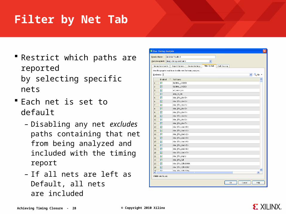
Filter by Net Tab
Restrict which paths are reported by selecting specific nets
Each net is set to default– Disabling any net excludes paths
containing that net from being analyzed and included with the timing report
– If all nets are left as Default, all nets are included
Achieving Timing Closure - 29 © Copyright 2010 Xilinx
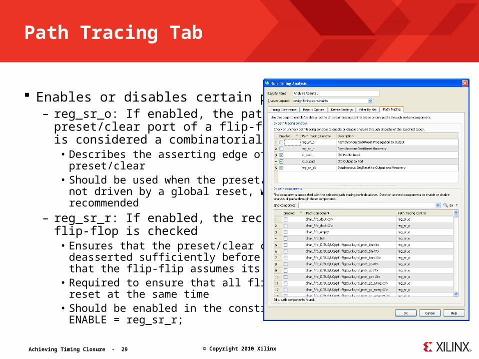
Path Tracing Tab
Enables or disables certain propagation paths– reg_sr_o: If enabled, the path from the async
preset/clear port of a flip-flop to the output is considered a combinatorial path
• Describes the asserting edge of the preset/clear
• Should be used when the preset/clear is not driven by a global reset, which is not recommended
– reg_sr_r: If enabled, the recovery arc of the flip-flop is checked
• Ensures that the preset/clear condition was deasserted sufficiently before the clock to ensure that the flip-flip assumes its non-reset behavior
• Required to ensure that all flip-flops come out of reset at the same time
• Should be enabled in the constraints:ENABLE = reg_sr_r;

Achieving Timing Closure - 30 © Copyright 2010 Xilinx
Summary
Timing reports enable you to determine how and why constraints were not met
Use the Synthesis Report and Post-Map Static Timing Report to estimate performance before running Place & Route
The detailed path description offers clues to the cause of timing failures Cross-probe to see the placement and a technology view of a timing path The Timing Analyzer can generate various types of reports for specific
circumstances