Embed Size (px)
Citation preview

Active damping of grid-connectedconverters with LCL filter
Comparison of common methods and further development
Mikkel RindholtEnergy Technology, OES10-2-F19
Master Thesis
ST
U
DE
NT R E P O R T

Copyright c© Aalborg University 2019
In compilation of this report, LATEX is used as writing program. The same program hasbeen used for constructing tables in the report. Graphs are constructed using MATLAB andsimulations are created in Simulink. All pictures taken of the internet, have the appropriateciting.
Institute of Energy Technology
Aalborg University Esbjerg
www.et.aau.dk
Title:Active damping of grid-connected con-verters with LCL filter
Theme:Power Electronic Systems
Project Period:Spring Semester 2019
Project Group:OES10-2-F19
Participant(s):Mikkel Rindholt
Supervisor(s):Amin Hajizadeh
Copies: 1
Page Numbers: 79
Date of Completion:May 30, 2019
Abstract:
For a Voltage Source Inverter (VSI), anLCL filter is one of the preferred filtermethods for obtaining a close to pure si-nusoidal output. Even though the LCLfilter itself generate harmonic distortionin the output, many methods have beeninvestigated to counteract this distor-tion. The method of using a damp-ing resister in series with the LCL fil-ter capacitor has proven effective, butat the cost of a significant amount ofpower losses. In this project three activedamping methods, PR control, Notchfilter and Virtual Resistor, are studied,and the Virtual Resistor chosen to re-place the damping resistor. A PI con-troller and the Virtual Resistor is de-signed and tested, both through simula-tions and lab. testing, and the LCL filtermodel is subsequently validated. Mean-while the concept of Adaptive VirtualResistance is also explored, and a algo-rithm for Minimal Distortion Trackingis developed and tested through simu-lations.
The content of this report is freely available, but publication (with reference) may only be pursued due to agreement
with the author.

Contents
Preface vii
1 Introduction 11.1 Inverter . . . . . . . . . . . . . . . . . . . . . . . . . . . . . . . . . . . . . . 21.2 LCL filter . . . . . . . . . . . . . . . . . . . . . . . . . . . . . . . . . . . . . 41.3 Damping Resistor . . . . . . . . . . . . . . . . . . . . . . . . . . . . . . . . 41.4 Grid standards . . . . . . . . . . . . . . . . . . . . . . . . . . . . . . . . . 5
2 Literature review 72.1 PR control method . . . . . . . . . . . . . . . . . . . . . . . . . . . . . . . 72.2 Notch filter method . . . . . . . . . . . . . . . . . . . . . . . . . . . . . . . 82.3 Virtual Resistor method . . . . . . . . . . . . . . . . . . . . . . . . . . . . 102.4 Conclusion . . . . . . . . . . . . . . . . . . . . . . . . . . . . . . . . . . . . 11
3 Modeling and design 133.1 Equation based model . . . . . . . . . . . . . . . . . . . . . . . . . . . . . 133.2 Model setup . . . . . . . . . . . . . . . . . . . . . . . . . . . . . . . . . . . 153.3 Setup specifications . . . . . . . . . . . . . . . . . . . . . . . . . . . . . . . 153.4 Controller design . . . . . . . . . . . . . . . . . . . . . . . . . . . . . . . . 163.5 Virtual Resistor . . . . . . . . . . . . . . . . . . . . . . . . . . . . . . . . . 16
4 Adaptive Virtual Resistance 214.1 Test of various operational conditions . . . . . . . . . . . . . . . . . . . . 214.2 Minimal Distortion Tracking for optimal resistance . . . . . . . . . . . . 234.3 Testing the Minimal Distortion Tracking algorithm . . . . . . . . . . . . 244.4 Conclusion . . . . . . . . . . . . . . . . . . . . . . . . . . . . . . . . . . . . 29
5 Lab Testing 315.1 Inverter setup . . . . . . . . . . . . . . . . . . . . . . . . . . . . . . . . . . 315.2 Implementation . . . . . . . . . . . . . . . . . . . . . . . . . . . . . . . . . 325.3 Optimization . . . . . . . . . . . . . . . . . . . . . . . . . . . . . . . . . . . 345.4 Validation test . . . . . . . . . . . . . . . . . . . . . . . . . . . . . . . . . . 36
Discussion 39
Conclusion 41
A Power Control of Grid Connected Converter for Offshore Wind Power Sys-tem 45
v


Preface
This project is a continuation of the work, described in the project “Power Control ofGrid Connected Converter for Offshore Wind Power System”. The project was donein collaboration with Hisham Hasan Taleb and Waqas Aslam Cheema. A copy of thethe project can be found in the appendix.
Aalborg University Esbjerg, May 30, 2019
Mikkel Rindholt<[email protected]>
vii

Chapter 1
Introduction
Most renewable energy producing devices, like wind turbines and solar panels, pro-duce a DC voltage, or AC voltage which is then rectified. To connect those devices tothe grid, an inverter is needed to convert the voltage into AC, which is synchronizedwith the grid voltage. The inverter output is not a pure sine wave but a modulatedsquare wave, which requires a filter, for the output to resemble a sine wave. One com-monly used filter is the LCL filter. This filter is effective at filtering the modulatedsquare wave, but due to the inductor-capacitor configuration, the filter also inducesharmonic distortion to the output sine wave. This has previously been connectinga damping resistor in series with the filter capacitor, to reduce that distortion. Thismethod is effective, but results in a power loss in the resister, which both reduce theeffectiveness of the DC to AC conversion, but also requires additional cooling, to re-move the heat, generated by the damping resistor.
This chapter will briefly describe the above mentioned terms; inverter, LCL filter,harmonic distortion and damping resistor.
1
2 Chapter 1. Introduction
1.1 Inverter
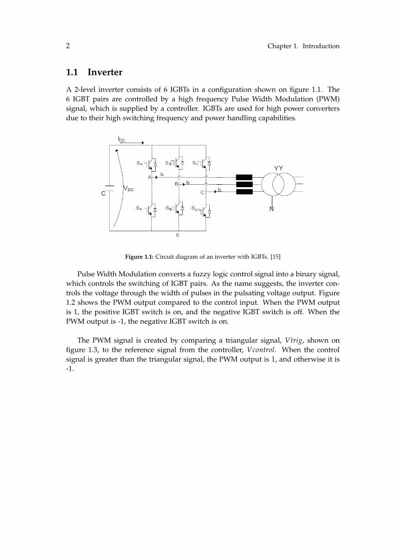
A 2-level inverter consists of 6 IGBTs in a configuration shown on figure 1.1. The6 IGBT pairs are controlled by a high frequency Pulse Width Modulation (PWM)signal, which is supplied by a controller. IGBTs are used for high power convertersdue to their high switching frequency and power handling capabilities.
Figure 1.1: Circuit diagram of an inverter with IGBTs. [15]
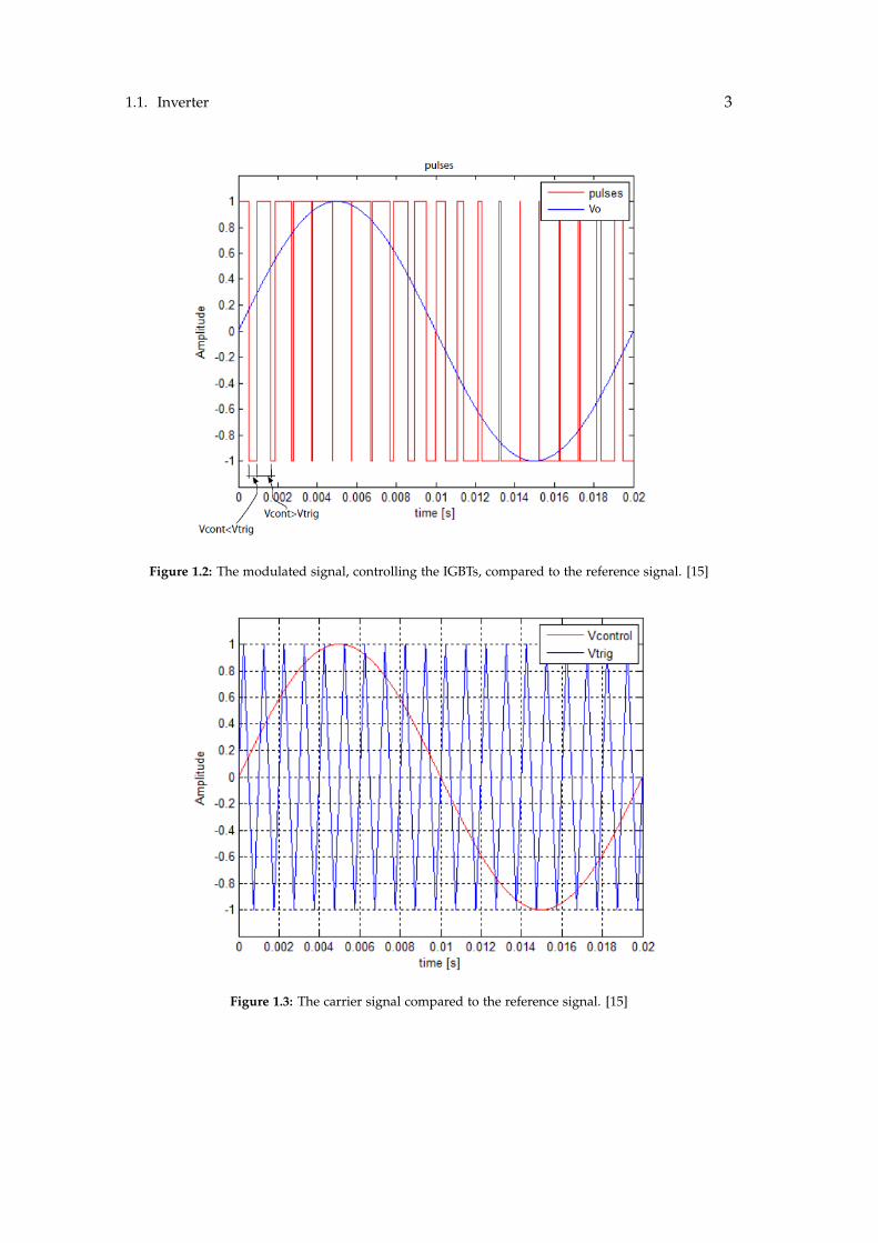
Pulse Width Modulation converts a fuzzy logic control signal into a binary signal,which controls the switching of IGBT pairs. As the name suggests, the inverter con-trols the voltage through the width of pulses in the pulsating voltage output. Figure1.2 shows the PWM output compared to the control input. When the PWM outputis 1, the positive IGBT switch is on, and the negative IGBT switch is off. When thePWM output is -1, the negative IGBT switch is on.
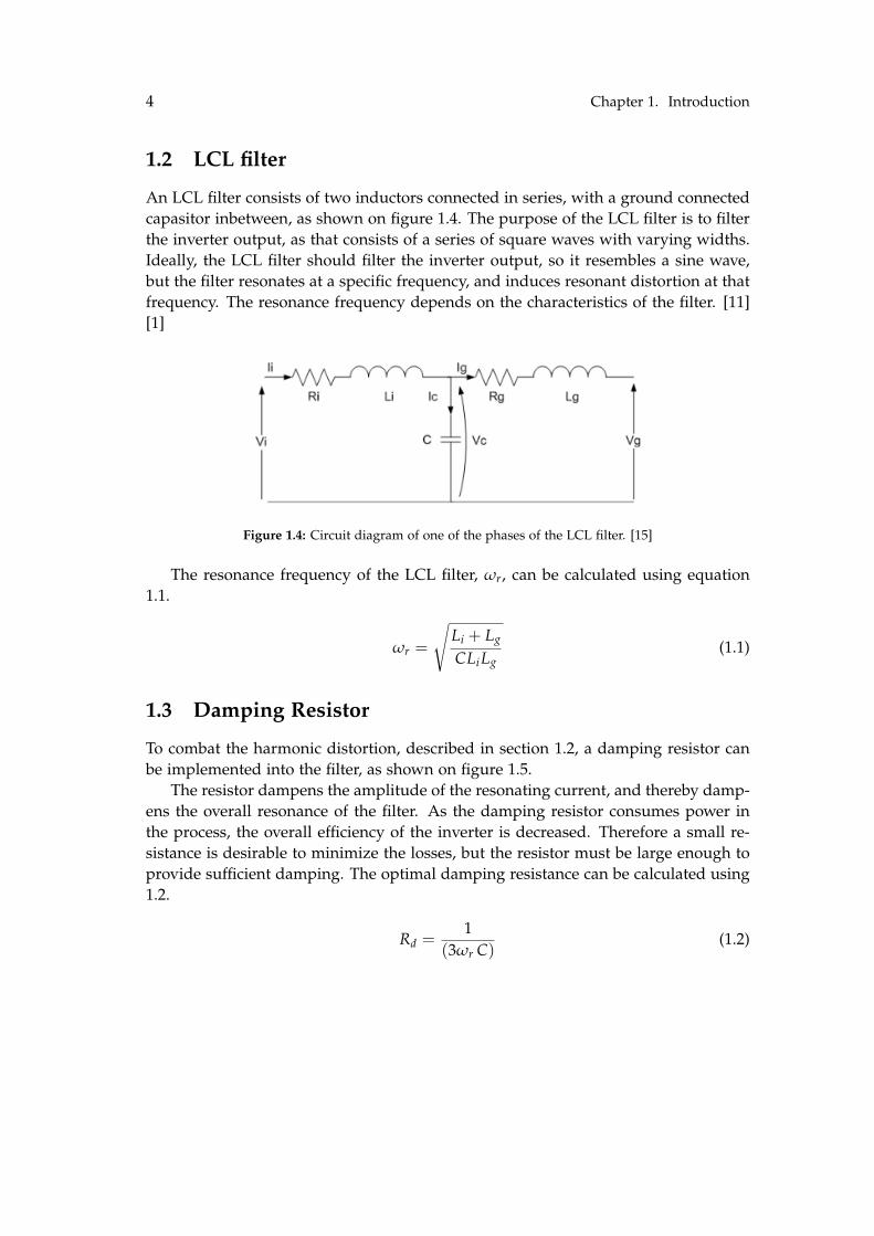
The PWM signal is created by comparing a triangular signal, Vtrig, shown onfigure 1.3, to the reference signal from the controller, Vcontrol. When the controlsignal is greater than the triangular signal, the PWM output is 1, and otherwise it is-1.
1.1. Inverter 3
Figure 1.2: The modulated signal, controlling the IGBTs, compared to the reference signal. [15]
Figure 1.3: The carrier signal compared to the reference signal. [15]
4 Chapter 1. Introduction
1.2 LCL filter
An LCL filter consists of two inductors connected in series, with a ground connectedcapasitor inbetween, as shown on figure 1.4. The purpose of the LCL filter is to filterthe inverter output, as that consists of a series of square waves with varying widths.Ideally, the LCL filter should filter the inverter output, so it resembles a sine wave,but the filter resonates at a specific frequency, and induces resonant distortion at thatfrequency. The resonance frequency depends on the characteristics of the filter. [11][1]
Figure 1.4: Circuit diagram of one of the phases of the LCL filter. [15]
The resonance frequency of the LCL filter, ωr, can be calculated using equation1.1.
ωr =
√Li + Lg
CLiLg(1.1)
1.3 Damping Resistor
To combat the harmonic distortion, described in section 1.2, a damping resistor canbe implemented into the filter, as shown on figure 1.5.
The resistor dampens the amplitude of the resonating current, and thereby damp-ens the overall resonance of the filter. As the damping resistor consumes power inthe process, the overall efficiency of the inverter is decreased. Therefore a small re-sistance is desirable to minimize the losses, but the resistor must be large enough toprovide sufficient damping. The optimal damping resistance can be calculated using1.2.
Rd =1
(3ωr C)(1.2)
1.4. Grid standards 5
Figure 1.5: Circuit diagram of one of the phases of the LCL filter with a damping resistor. [15]
1.4 Grid standards
Many national and international standards define the rules for grid-connected in-verters. This section will compare the standards for electrical characteristics of pho-tovoltaic grid-connected inverter systems, defined by the standards for the EuropeanUnion (IEC 61727:2004) and the United States (IEEE 1547:2018), in regards to har-monic current distortion.
Table 1.1: Comparison of the IEC and IEEE standards for harmonic current distortion. [13] [8]
IEC 61727:2004 IEEE 1547:2018Odd Harmonics Threshold in % Threshold in %
≤ 9th < 4.0 ≤ 4.011th to 17th < 2.0 ≤ 2.017th to 23th < 1.5 ≤ 1.523th to 35th < 0.6 ≤ 0.635th to 50th - ≤ 0.3
Even Harmonics Threshold in % Threshold in %2th
< 1.0
≤ 1.04th ≤ 2.06th ≤ 3.08th ≤ 4.0
10th to 14th < 0.5 ≤ 2.016th to 20th < 0.5 ≤ 1.522th to 34th < 0.5 ≤ 0.636th to 50th - ≤ 0.3
Total Rated Distortion < 5.0 ≤ 5.0
These two standards have similar requirements for the odd harmonics, but theupdated IEEE 1547 have changed requirements for the even harmonics. [5]

6 Chapter 1. Introduction
In the latest version of the IEEE 1547 standard, the term current THD has beenreplaced with Total Rated Distortion (TRD), where inter-harmonic distortion is in-cluded into the total distortion calculations as well. Inter-harmonic distortion is dis-tortion from frequencies, which are not harmonic components of the fundamentalfrequency. These changes might be included in a future, amended version of the IEC61727 standard as well, as the current version will expire in 2022. [13]For this project the results will be compared with the 5% limit for current THD,described in the IEC 61727:2004 standard.
Chapter 2
Literature review
This literature review will investigate scientific papers regarding active damping ofharmonic distortion induced in an LCL filter, as described in chapter 1. The reviewwill focus on papers describing different active control methods for reducing thistype of distortion. Three active control methods have been selected for the review.These methods are PR-controller, Notch filter and Virtual Resister.
Improved passive filters methods, to reduce the power losses several differentsolutions have also been investigated, e.g. different configurations of resistors, in-ductors and capacitors to minimize the losses while still obtaining the same dampingeffect. [20] [18]
The common result of these solutions is reduced losses, while still maintainingan effective reduction of the distortion. However, contrary to the active dampingmethods, these methods do still result in losses, which is one of the key problems,that should be eliminated. Therefore, these methods will not be investigated furtherin this report.
2.1 PR control method
The Proportional-Resonant control method is similar to a PID controller. A PR con-troller is utilizing the same proportional control method, but instead of an integraland derivative component, is has a resonant component that filter resonance at aspecific frequency. The controller is, like the PID controller, tuned by changing theKp and Kr, but the harmonic resonance frequency, ωr, is also needed to design thiscontroller. [2]
GPR(s) = Kp +Kr s
s2 + ωr2 (2.1)
The PR controller transfer-function 2.1 is the ideal controller, which filter out anynoise at the specified resonance frequency. It will, however, result in an infinite gainat the resonant frequency, which should be avoided due to system instability. [16]
GPR(s) = Kp +Kr ωc s
s2 + ωc2s + ωr(2.2)
7
8 Chapter 2. Literature review
In the non-ideal PR controller transfer-function 2.2, a cutoff frequency ωc is intro-duced to control the bandwidth of the controller. [17]
This controller works on a stationary reference frame, meaning no phase angledetection is required. In some controller layouts, where one or more reference inputsare in a rotating reference frame, this will still be necessary for conversion into astationary reference frame.
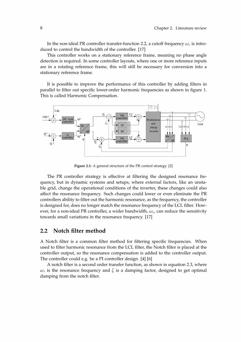
It is possible to improve the performance of this controller by adding filters inparallel to filter out specific lower-order harmonic frequencies as shown in figure 1.This is called Harmonic Compensation.
Figure 2.1: A general structure of the PR control strategy. [2]
The PR controller strategy is effective at filtering the designed resonance fre-quency, but in dynamic systems and setups, where external factors, like an unsta-ble grid, change the operational conditions of the inverter, these changes could alsoaffect the resonance frequency. Such changes could lower or even eliminate the PRcontrollers ability to filter out the harmonic resonance, as the frequency, the controlleris designed for, does no longer match the resonance frequency of the LCL filter. How-ever, for a non-ideal PR controller, a wider bandwidth, ωc, can reduce the sensitivitytowards small variations in the resonance frequency. [17]
2.2 Notch filter method
A Notch filter is a common filter method for filtering specific frequencies. Whenused to filter harmonic resonance from the LCL filter, the Notch filter is placed at thecontroller output, so the resonance compensation is added to the controller output.The controller could e.g. be a PI controller design. [4] [6]
A notch filter is a second order transfer function, as shown in equation 2.3, whereωr is the resonance frequency and ζ is a damping factor, designed to get optimaldamping from the notch filter.

2.2. Notch filter method 9
Figure 2.2: A block diagram of the notch filter method
Gnotch(s) =s2 + ωr
2
s2 + 2ζ ωr s + ωr2 (2.3)
The notch filter, like the PR controller, is designed to filter out any resonant dis-tortion at one specific frequency, so any changes to the operational conditions couldchange the resonance frequency of the LCL-filter and therefore make the Notch filterunable to filter out the distortion.
Another approach is to control the notch filter performance through a qualityfactor, q, as shown in equation 2.4. [19]
Gnotch(s) =s2 + ωr
2
s2 + 1q ωr s + ωr2
(2.4)
This approach, however, does not fundamentally change the Notch filter transfer-function, as the equations 2.3 and 2.4 only have different approaches to controllingthe damping behavior of the Notch filter.
A problem for notch filters is, that the filter transfer function cannot be discretized,while maintaining the desired damping frequency. The sampling frequency and dis-cretization method affect the center frequency of the discretized notch filter, and adiscrete notch filter has another design process than the continuous filter. [6]
A solution to this problem could be to design the Notch filter in a discrete from,as shown in equation 2.5. [3]
GNF(z) =12
[1 +
k2 + k1(1 + k2)z−1 + z−2)
1 + k1(1 + k2)z−1 + k2z−2
](2.5)
The constants k1 and k2 of discrete Notch filter can be calculated based on theinverter switching time, Tsw, the resonance frequency, fr, and the desired bandwidthof the Notch filter, BNF. These can also be changed in real-time, to compensate forchanges of the resonance frequency, caused by external factors.
k1 = −cos(Tsw · 2π · fr) and k2 =1 − tan(Tsw · 2π · BNF/2)1 + tan(Tsw · 2π · BNF/2)
(2.6)
10 Chapter 2. Literature review
The Notch filter method is effective at compensating for the resonance, also whenthe frequency is changing. A downside of the Notch filter is that it does compensatefor other harmonic frequencies, unlike the PR control method.
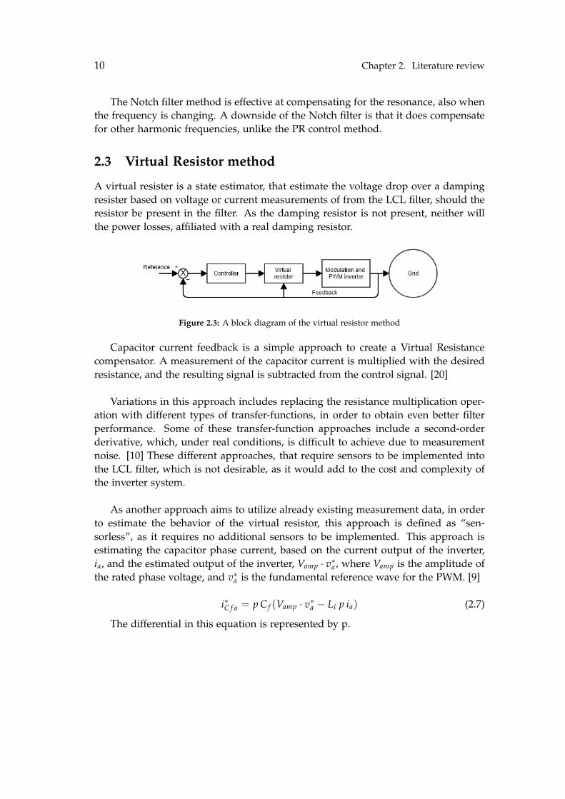
2.3 Virtual Resistor method
A virtual resister is a state estimator, that estimate the voltage drop over a dampingresister based on voltage or current measurements of from the LCL filter, should theresistor be present in the filter. As the damping resistor is not present, neither willthe power losses, affiliated with a real damping resistor.
Figure 2.3: A block diagram of the virtual resistor method
Capacitor current feedback is a simple approach to create a Virtual Resistancecompensator. A measurement of the capacitor current is multiplied with the desiredresistance, and the resulting signal is subtracted from the control signal. [20]
Variations in this approach includes replacing the resistance multiplication oper-ation with different types of transfer-functions, in order to obtain even better filterperformance. Some of these transfer-function approaches include a second-orderderivative, which, under real conditions, is difficult to achieve due to measurementnoise. [10] These different approaches, that require sensors to be implemented intothe LCL filter, which is not desirable, as it would add to the cost and complexity ofthe inverter system.
As another approach aims to utilize already existing measurement data, in orderto estimate the behavior of the virtual resistor, this approach is defined as “sen-sorless”, as it requires no additional sensors to be implemented. This approach isestimating the capacitor phase current, based on the current output of the inverter,ia, and the estimated output of the inverter, Vamp · v∗a , where Vamp is the amplitude ofthe rated phase voltage, and v∗a is the fundamental reference wave for the PWM. [9]
i∗C f a = p C f (Vamp · v∗a − Li p ia) (2.7)
The differential in this equation is represented by p.
2.4. Conclusion 11
As with the PR controller ands Notch filter methods, grid disturbances could af-fect the performance of the Virtual Resistor. One method attempts to address thismatter by detecting grid impedance variation, and based on that adapt the VirtualResistance to optimize the damping performance. [7]
Unlike the PR controller ands Notch filter methods, the Virtual Resistance methoddoes not depend on a specific resonance frequency, but rather the currents, runninginside the LCL filter, which can be estimated without the need for additional sen-sors. The Virtual Resistance method seems less effective at filtering out the specificresonance frequency, but overall more effective at filtering general distortion.
2.4 Conclusion
Many methods exist to eliminate the harmonic resonance from the LCL filter.
While the PR controller and Notch filter are effective at filtering out resonancefrom specific resonance frequencies, they lack the robustness of the damping resis-tor. The Virtual Resistance method approaches the problem from a different angle,by imitating the behavior of the damping resistor, and thereby obtaining a similarrobustness as the damping resistor. However, the Virtual Resistor does not have thesame filtering performance at the specific resonance frequencies, but it has an overalladvantage, as it can filter many different harmonic frequencies with a single filter.
As the goal of this project is to find a robust solution to the resonance problem,the Virtual Resistance method is chosen, as it seems to provide sufficient robustnessover the two other methods.

Chapter 3
Modeling and design
3.1 Equation based model
This model is based on a reference model described in the project “Power Control ofGrid Connected Converter for Offshore Wind Power System”[15]. Several improve-ments have been made to parts of the model, and will be described in this chapter,but the general aspects of the model remain the same, and this will be noted in thespecific descriptions.
Inverter model
This inverter model, unlike in the reference model, is not an average model of aninverter, as the PWM switching pattern is the primary reason for the need of an LCLfilter. In this improved model, the input from the controller is converted into a properPWM signal, as described in chapter 1, section 1.1. This signal is then multiplied bythe DC-link voltage to generate a modulated voltage output, almost as a real inverterwould make. This model is based the ideal behavior of IGBTs, which does not accountfor the switching dynamics, like inductive kicks, of IGBTs and is therefore not 100%accurate.
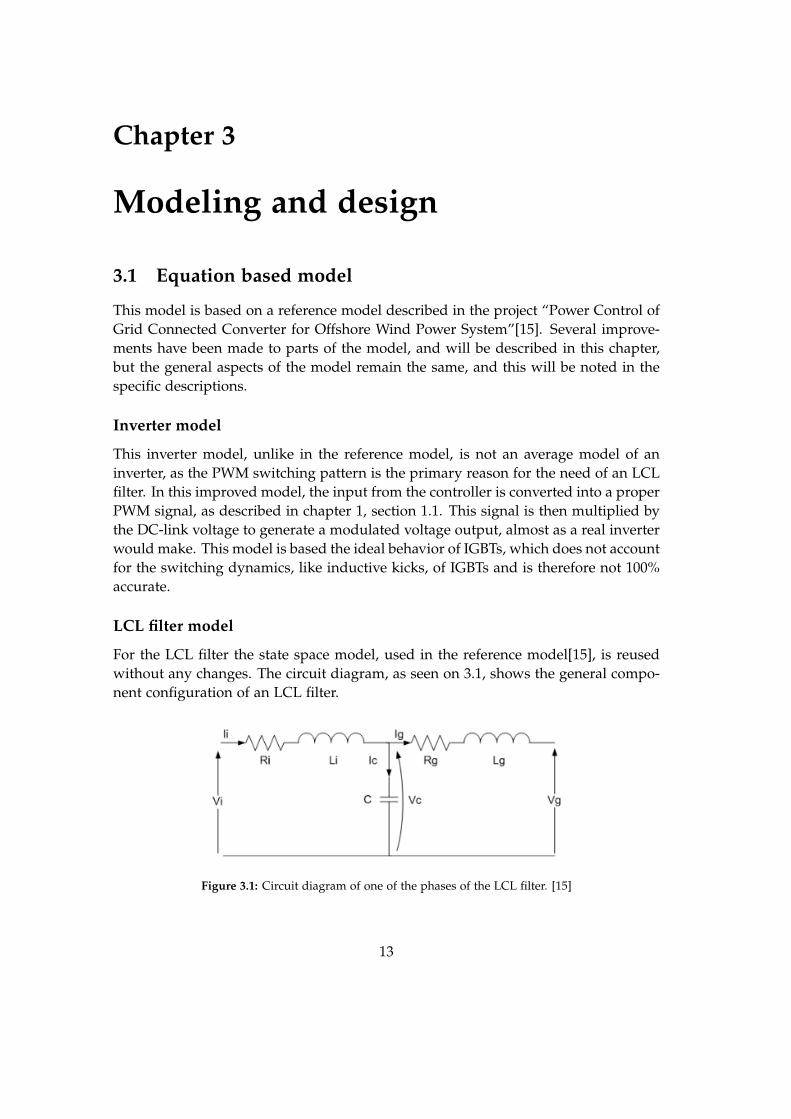
LCL filter model
For the LCL filter the state space model, used in the reference model[15], is reusedwithout any changes. The circuit diagram, as seen on 3.1, shows the general compo-nent configuration of an LCL filter.
Figure 3.1: Circuit diagram of one of the phases of the LCL filter. [15]
13
14 Chapter 3. Modeling and design
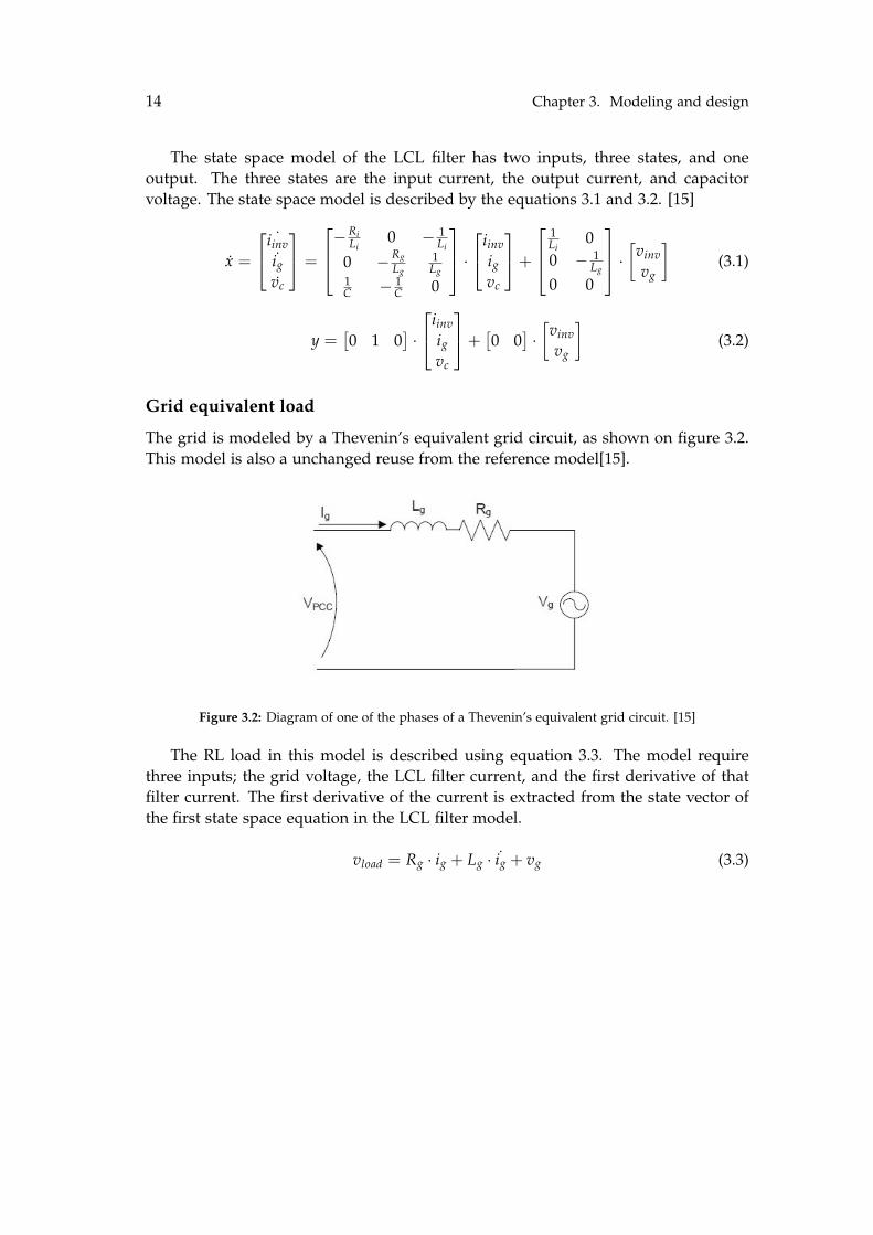
The state space model of the LCL filter has two inputs, three states, and oneoutput. The three states are the input current, the output current, and capacitorvoltage. The state space model is described by the equations 3.1 and 3.2. [15]
x =
˙iinv˙ig
vc
=
−RiLi
0 − 1Li
0 −RgLg
1Lg
1C − 1
C 0
·
iinvig
vc
+
1Li
00 − 1
Lg
0 0
·[
vinvvg
](3.1)
y =[0 1 0
]·
iinvig
vc
+[0 0
]·[
vinvvg
](3.2)
Grid equivalent load
The grid is modeled by a Thevenin’s equivalent grid circuit, as shown on figure 3.2.This model is also a unchanged reuse from the reference model[15].
Figure 3.2: Diagram of one of the phases of a Thevenin’s equivalent grid circuit. [15]
The RL load in this model is described using equation 3.3. The model requirethree inputs; the grid voltage, the LCL filter current, and the first derivative of thatfilter current. The first derivative of the current is extracted from the state vector ofthe first state space equation in the LCL filter model.
vload = Rg · ig + Lg · ˙ig + vg (3.3)
3.2. Model setup 15
3.2 Model setup
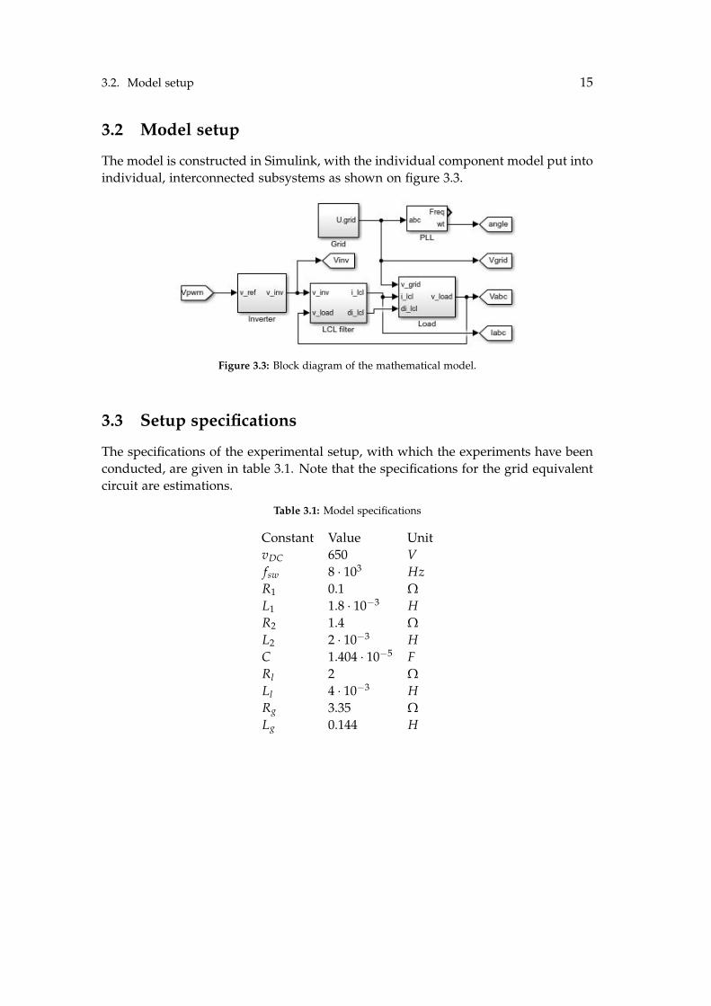
The model is constructed in Simulink, with the individual component model put intoindividual, interconnected subsystems as shown on figure 3.3.
Figure 3.3: Block diagram of the mathematical model.
3.3 Setup specifications
The specifications of the experimental setup, with which the experiments have beenconducted, are given in table 3.1. Note that the specifications for the grid equivalentcircuit are estimations.
Table 3.1: Model specifications
Constant Value UnitvDC 650 Vfsw 8 · 103 HzR1 0.1 ΩL1 1.8 · 10−3 HR2 1.4 ΩL2 2 · 10−3 HC 1.404 · 10−5 FRl 2 ΩLl 4 · 10−3 HRg 3.35 ΩLg 0.144 H
16 Chapter 3. Modeling and design
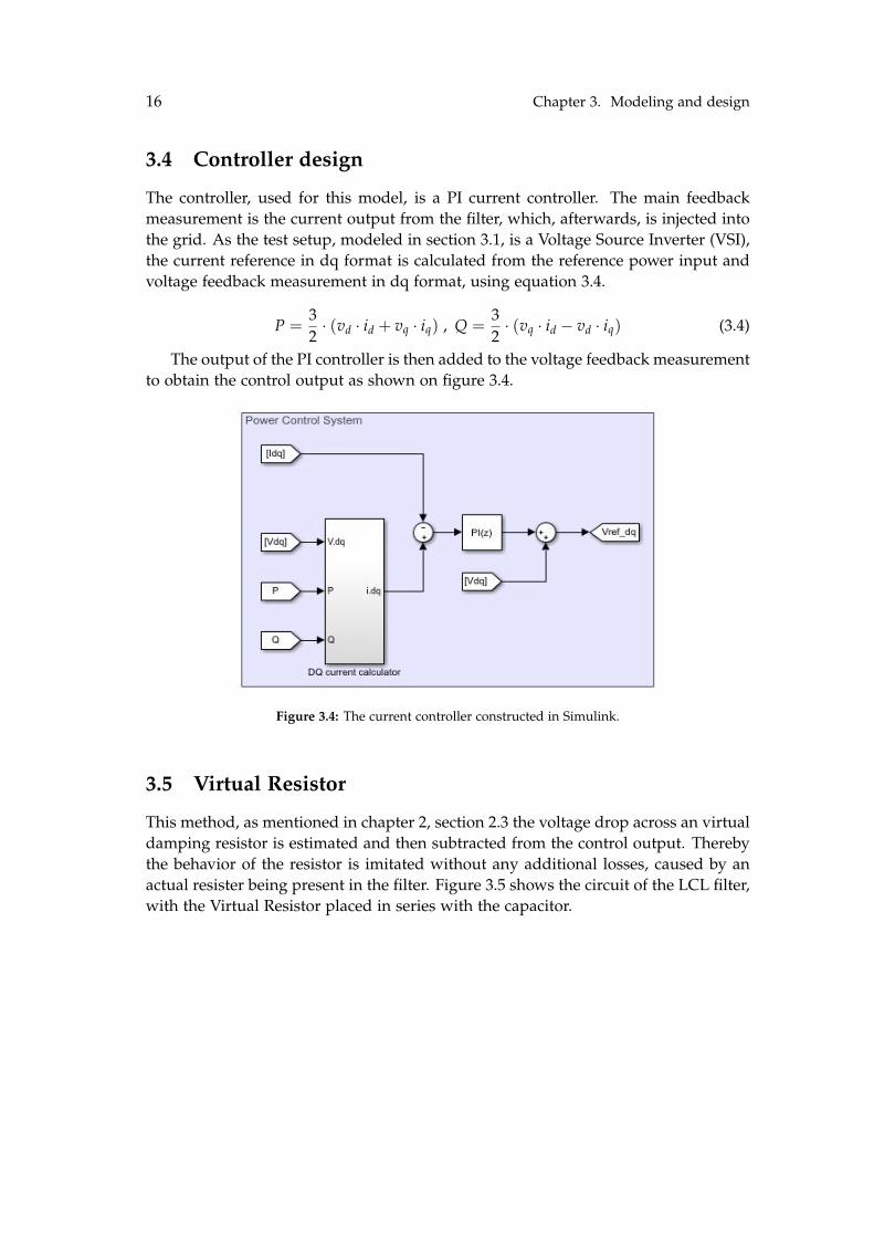
3.4 Controller design
The controller, used for this model, is a PI current controller. The main feedbackmeasurement is the current output from the filter, which, afterwards, is injected intothe grid. As the test setup, modeled in section 3.1, is a Voltage Source Inverter (VSI),the current reference in dq format is calculated from the reference power input andvoltage feedback measurement in dq format, using equation 3.4.
P =32· (vd · id + vq · iq) , Q =
32· (vq · id − vd · iq) (3.4)
The output of the PI controller is then added to the voltage feedback measurementto obtain the control output as shown on figure 3.4.
Figure 3.4: The current controller constructed in Simulink.
3.5 Virtual Resistor
This method, as mentioned in chapter 2, section 2.3 the voltage drop across an virtualdamping resistor is estimated and then subtracted from the control output. Therebythe behavior of the resistor is imitated without any additional losses, caused by anactual resister being present in the filter. Figure 3.5 shows the circuit of the LCL filter,with the Virtual Resistor placed in series with the capacitor.
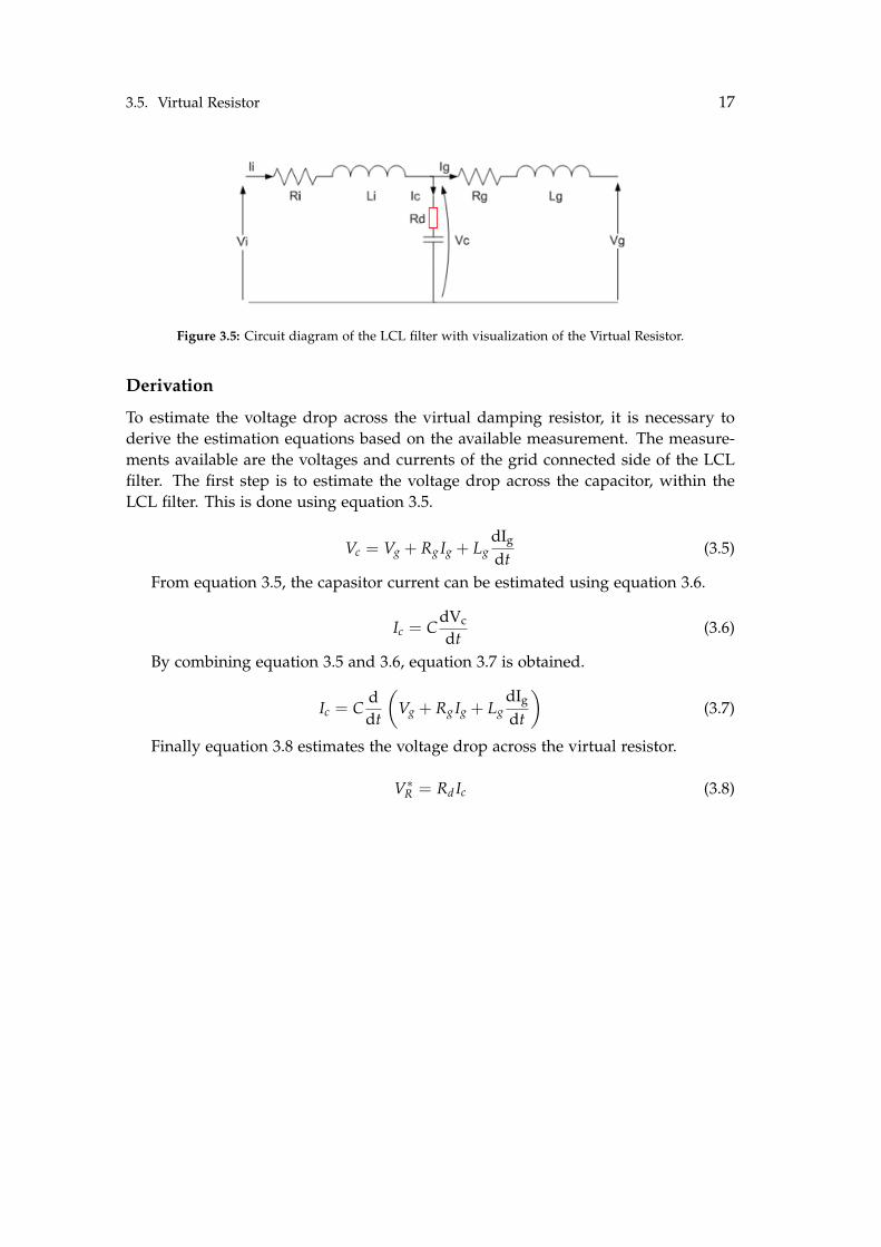
3.5. Virtual Resistor 17
Figure 3.5: Circuit diagram of the LCL filter with visualization of the Virtual Resistor.
Derivation
To estimate the voltage drop across the virtual damping resistor, it is necessary toderive the estimation equations based on the available measurement. The measure-ments available are the voltages and currents of the grid connected side of the LCLfilter. The first step is to estimate the voltage drop across the capacitor, within theLCL filter. This is done using equation 3.5.
Vc = Vg + Rg Ig + LgdIg
dt(3.5)
From equation 3.5, the capasitor current can be estimated using equation 3.6.
Ic = CdVc
dt(3.6)
By combining equation 3.5 and 3.6, equation 3.7 is obtained.
Ic = Cddt
(Vg + Rg Ig + Lg
dIg
dt
)(3.7)
Finally equation 3.8 estimates the voltage drop across the virtual resistor.
V∗R = Rd Ic (3.8)
18 Chapter 3. Modeling and design
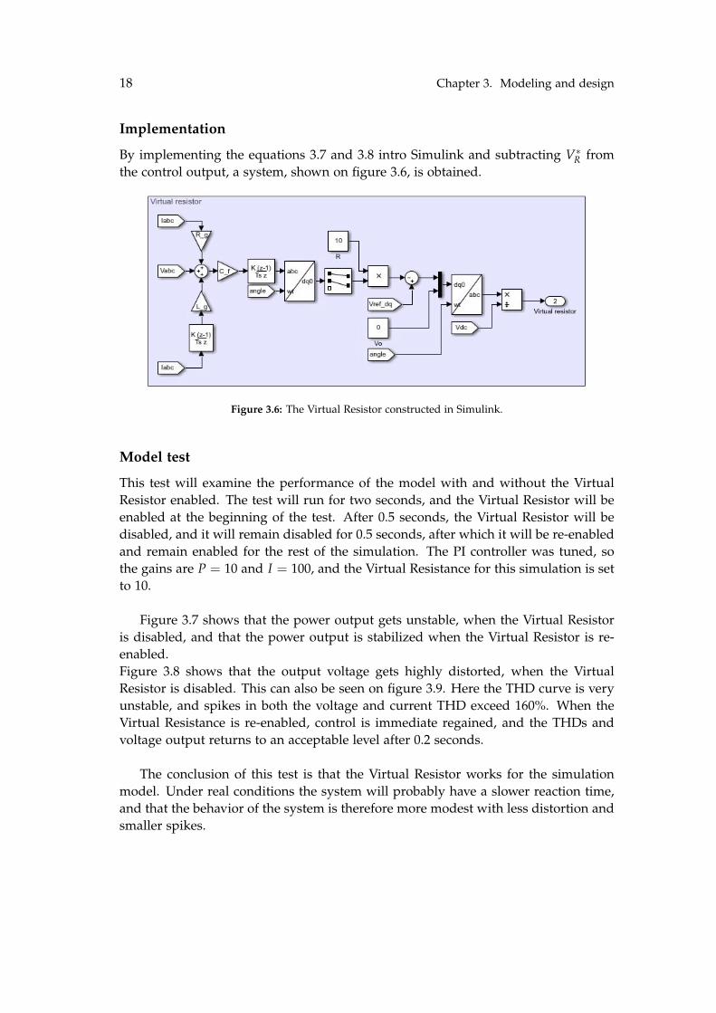
Implementation
By implementing the equations 3.7 and 3.8 intro Simulink and subtracting V∗R from
the control output, a system, shown on figure 3.6, is obtained.
Figure 3.6: The Virtual Resistor constructed in Simulink.
Model test
This test will examine the performance of the model with and without the VirtualResistor enabled. The test will run for two seconds, and the Virtual Resistor will beenabled at the beginning of the test. After 0.5 seconds, the Virtual Resistor will bedisabled, and it will remain disabled for 0.5 seconds, after which it will be re-enabledand remain enabled for the rest of the simulation. The PI controller was tuned, sothe gains are P = 10 and I = 100, and the Virtual Resistance for this simulation is setto 10.
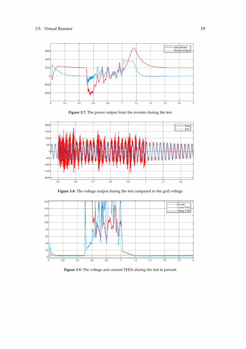
Figure 3.7 shows that the power output gets unstable, when the Virtual Resistoris disabled, and that the power output is stabilized when the Virtual Resistor is re-enabled.Figure 3.8 shows that the output voltage gets highly distorted, when the VirtualResistor is disabled. This can also be seen on figure 3.9. Here the THD curve is veryunstable, and spikes in both the voltage and current THD exceed 160%. When theVirtual Resistance is re-enabled, control is immediate regained, and the THDs andvoltage output returns to an acceptable level after 0.2 seconds.
The conclusion of this test is that the Virtual Resistor works for the simulationmodel. Under real conditions the system will probably have a slower reaction time,and that the behavior of the system is therefore more modest with less distortion andsmaller spikes.
3.5. Virtual Resistor 19
Figure 3.7: The power output from the inverter during the test
Figure 3.8: The voltage output during the test compared to the grid voltage
Figure 3.9: The voltage and current THDs during the test in percent

Chapter 4
Adaptive Virtual Resistance
The optimal Virtual Resistance under consistent nominal operation will remain con-stant, but for renewable energy-producing, grid-connected, devices the operationconditions are dynamic due to various factors. The power output and grid condi-tions change constantly, which affects the currents running inside the inverter andfilter, and thereby the harmonic currents. Therefore it can be assumed that the opti-mal Virtual Resistance will not be the same under all operational conditions.
4.1 Test of various operational conditions
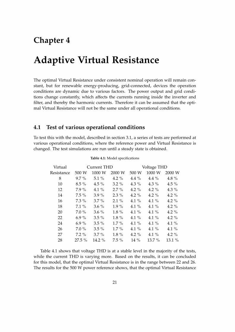
To test this with the model, described in section 3.1, a series of tests are performed atvarious operational conditions, where the reference power and Virtual Resistance ischanged. The test simulations are run until a steady state is obtained.
Table 4.1: Model specifications
VirtualResistance
Current THD Voltage THD500 W 1000 W 2000 W 500 W 1000 W 2000 W
8 9.7 % 5.1 % 4.2 % 4.4 % 4.4 % 4.8 %10 8.5 % 4.5 % 3.2 % 4.3 % 4.3 % 4.5 %12 7.9 % 4.1 % 2.7 % 4.2 % 4.2 % 4.3 %14 7.5 % 3.9 % 2.3 % 4.2 % 4.2 % 4.2 %16 7.3 % 3.7 % 2.1 % 4.1 % 4.1 % 4.2 %18 7.1 % 3.6 % 1.9 % 4.1 % 4.1 % 4.2 %20 7.0 % 3.6 % 1.8 % 4.1 % 4.1 % 4.2 %22 6.9 % 3.5 % 1.8 % 4.1 % 4.1 % 4.2 %24 6.9 % 3.5 % 1.7 % 4.1 % 4.1 % 4.1 %26 7.0 % 3.5 % 1.7 % 4.1 % 4.1 % 4.1 %27 7.2 % 3.7 % 1.8 % 4.2 % 4.1 % 4.2 %28 27.5 % 14.2 % 7.5 % 14 % 13.7 % 13.1 %
Table 4.1 shows that voltage THD is at a stable level in the majority of the tests,while the current THD is varying more. Based on the results, it can be concludedfor this model, that the optimal Virtual Resistance is in the range between 22 and 26.The results for the 500 W power reference shows, that the optimal Virtual Resistance
21
22 Chapter 4. Adaptive Virtual Resistance
would be approximately 23, while it would be approximately 24 at 1000 W and 25at 2000 W. In a real test, where the distortion would be greater, it would be assumedthat the differences would be more significant.
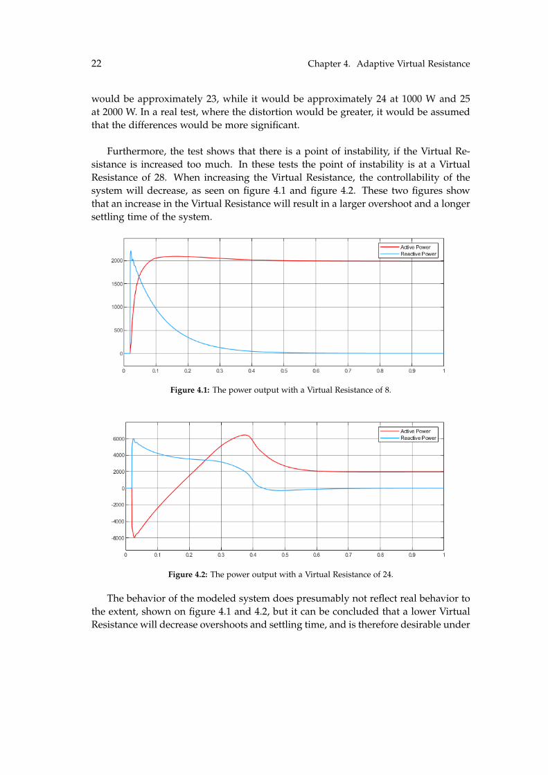
Furthermore, the test shows that there is a point of instability, if the Virtual Re-sistance is increased too much. In these tests the point of instability is at a VirtualResistance of 28. When increasing the Virtual Resistance, the controllability of thesystem will decrease, as seen on figure 4.1 and figure 4.2. These two figures showthat an increase in the Virtual Resistance will result in a larger overshoot and a longersettling time of the system.
Figure 4.1: The power output with a Virtual Resistance of 8.
Figure 4.2: The power output with a Virtual Resistance of 24.
The behavior of the modeled system does presumably not reflect real behavior tothe extent, shown on figure 4.1 and 4.2, but it can be concluded that a lower VirtualResistance will decrease overshoots and settling time, and is therefore desirable under
4.2. Minimal Distortion Tracking for optimal resistance 23
conditions, where there is a large difference between the reference and feedbackvalues in the system.
4.2 Minimal Distortion Tracking for optimal resistance
As shown in section 4.1, the optimal Virtual Resistance increase when the poweroutput increase. In this test the power output quadrupled, but for most renewableenergy-producing devices the power output range is larger. Therefore the range ofoptimal Virtual Resistance will be significant, and from that it can be assumed, thattracking the optimum could improve the overall performance of the inverter.
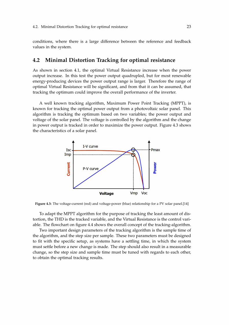
A well known tracking algorithm, Maximum Power Point Tracking (MPPT), isknown for tracking the optimal power output from a photovoltaic solar panel. Thisalgorithm is tracking the optimum based on two variables; the power output andvoltage of the solar panel. The voltage is controlled by the algorithm and the changein power output is tracked in order to maximize the power output. Figure 4.3 showsthe characteristics of a solar panel.
Figure 4.3: The voltage-current (red) and voltage-power (blue) relationship for a PV solar panel.[14]
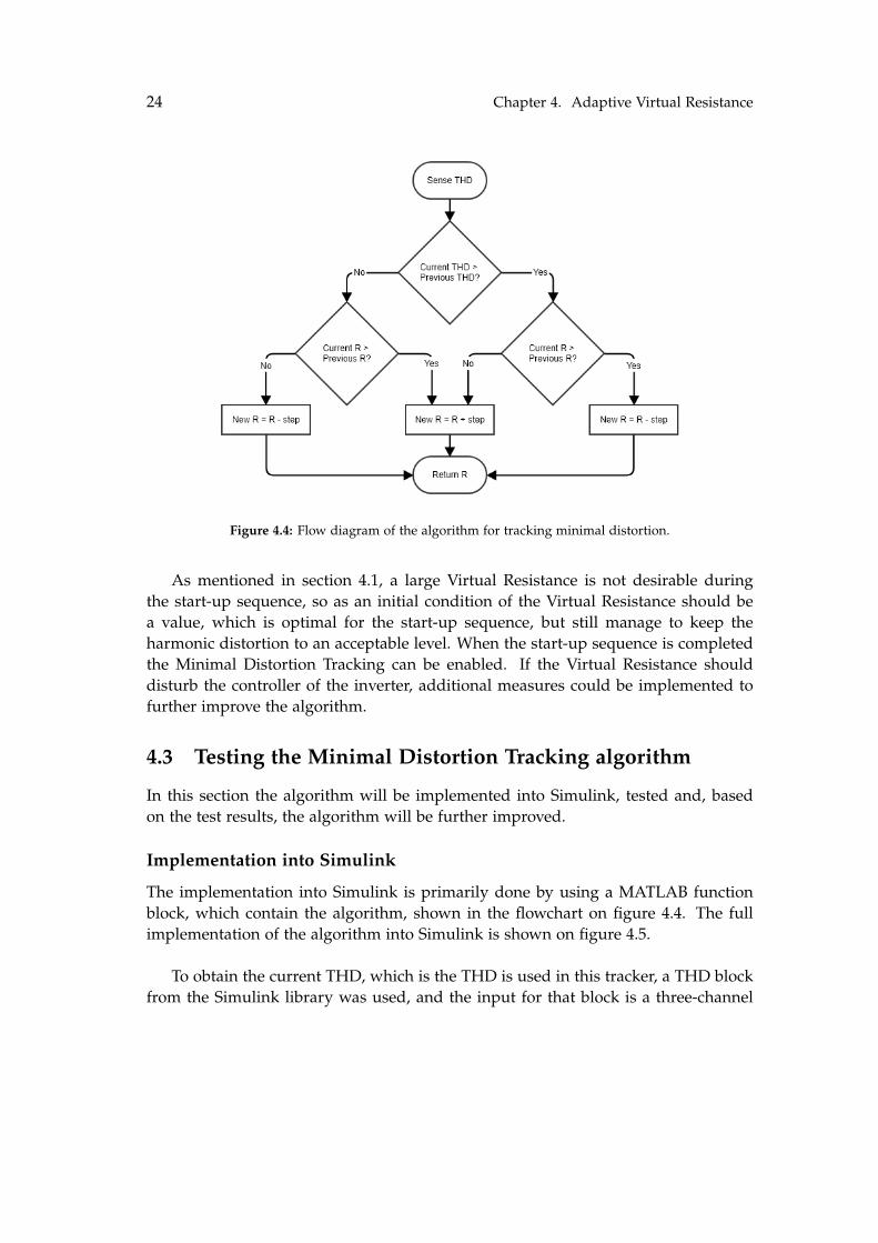
To adapt the MPPT algorithm for the purpose of tracking the least amount of dis-tortion, the THD is the tracked variable, and the Virtual Resistance is the control vari-able. The flowchart on figure 4.4 shows the overall concept of the tracking-algorithm.
Two important design parameters of the tracking algorithm is the sample time ofthe algorithm, and the step size per sample. These two parameters must be designedto fit with the specific setup, as systems have a settling time, in which the systemmust settle before a new change is made. The step should also result in a measurablechange, so the step size and sample time must be tuned with regards to each other,to obtain the optimal tracking results.
24 Chapter 4. Adaptive Virtual Resistance
Figure 4.4: Flow diagram of the algorithm for tracking minimal distortion.
As mentioned in section 4.1, a large Virtual Resistance is not desirable duringthe start-up sequence, so as an initial condition of the Virtual Resistance should bea value, which is optimal for the start-up sequence, but still manage to keep theharmonic distortion to an acceptable level. When the start-up sequence is completedthe Minimal Distortion Tracking can be enabled. If the Virtual Resistance shoulddisturb the controller of the inverter, additional measures could be implemented tofurther improve the algorithm.
4.3 Testing the Minimal Distortion Tracking algorithm
In this section the algorithm will be implemented into Simulink, tested and, basedon the test results, the algorithm will be further improved.
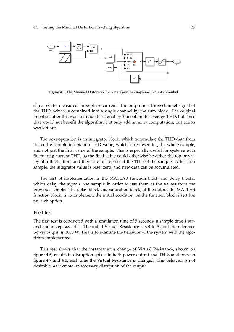
Implementation into Simulink
The implementation into Simulink is primarily done by using a MATLAB functionblock, which contain the algorithm, shown in the flowchart on figure 4.4. The fullimplementation of the algorithm into Simulink is shown on figure 4.5.
To obtain the current THD, which is the THD is used in this tracker, a THD blockfrom the Simulink library was used, and the input for that block is a three-channel
4.3. Testing the Minimal Distortion Tracking algorithm 25
Figure 4.5: The Minimal Distortion Tracking algorithm implemented into Simulink.
signal of the measured three-phase current. The output is a three-channel signal ofthe THD, which is combined into a single channel by the sum block. The originalintention after this was to divide the signal by 3 to obtain the average THD, but sincethat would not benefit the algorithm, but only add an extra computation, this actionwas left out.
The next operation is an integrator block, which accumulate the THD data fromthe entire sample to obtain a THD value, which is representing the whole sample,and not just the final value of the sample. This is especially useful for systems withfluctuating current THD, as the final value could otherwise be either the top or val-ley of a fluctuation, and therefore misrepresent the THD of the sample. After eachsample, the integrator value is reset zero, and new data can be accumulated.
The rest of implementation is the MATLAB function block and delay blocks,which delay the signals one sample in order to use them at the values from theprevious sample. The delay block and saturation block, at the output the MATLABfunction block, is to implement the initial condition, as the function block itself hasno such option.
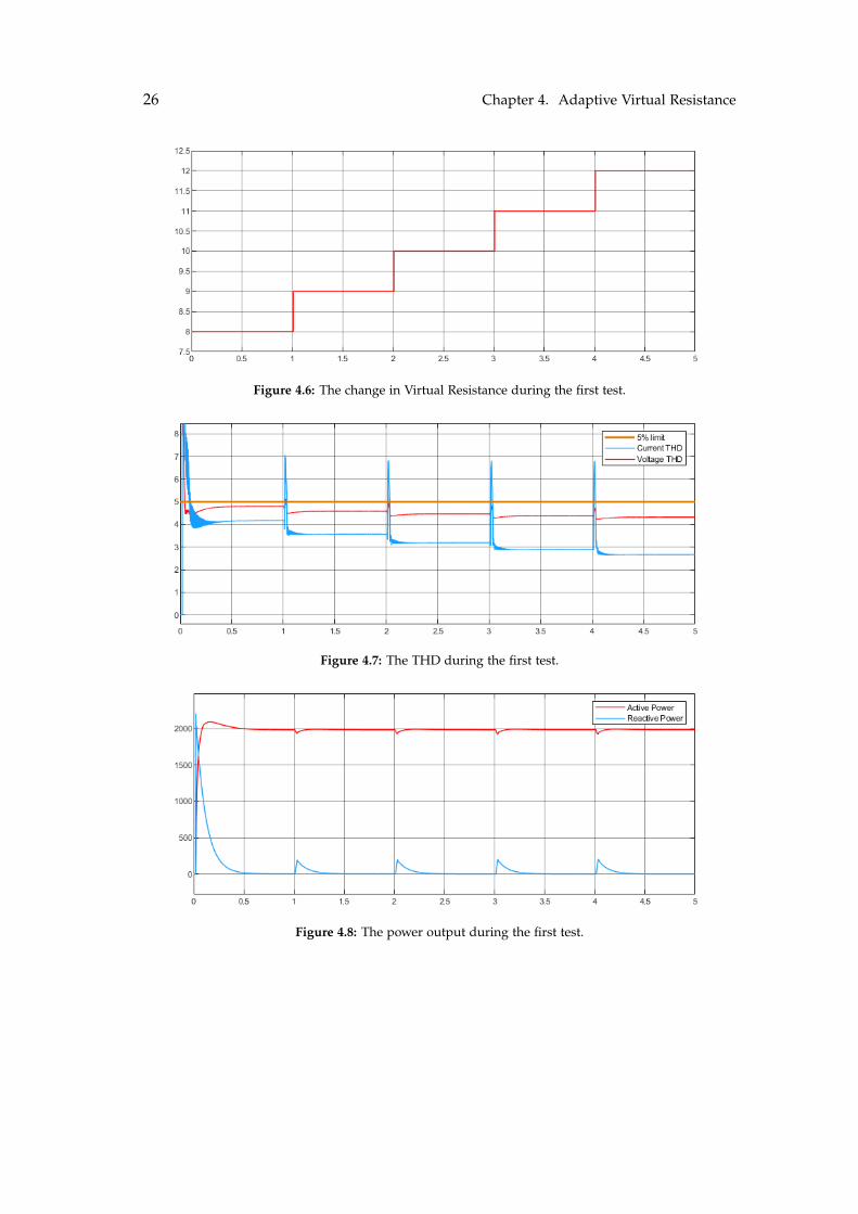
First test
The first test is conducted with a simulation time of 5 seconds, a sample time 1 sec-ond and a step size of 1. The initial Virtual Resistance is set to 8, and the referencepower output is 2000 W. This is to examine the behavior of the system with the algo-rithm implemented.
This test shows that the instantaneous change of Virtual Resistance, shown onfigure 4.6, results in disruption spikes in both power output and THD, as shown onfigure 4.7 and 4.8, each time the Virtual Resistance is changed. This behavior is notdesirable, as it create unnecessary disruption of the output.
26 Chapter 4. Adaptive Virtual Resistance
Figure 4.6: The change in Virtual Resistance during the first test.
Figure 4.7: The THD during the first test.
Figure 4.8: The power output during the first test.
4.3. Testing the Minimal Distortion Tracking algorithm 27
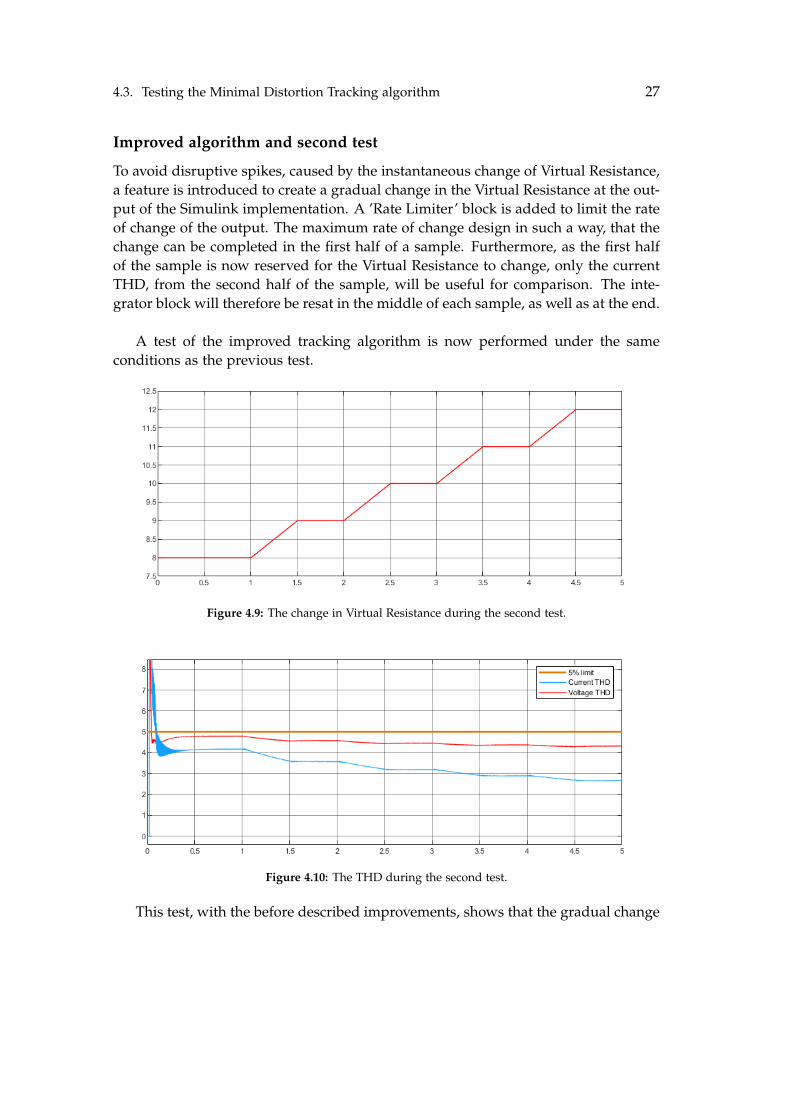
Improved algorithm and second test
To avoid disruptive spikes, caused by the instantaneous change of Virtual Resistance,a feature is introduced to create a gradual change in the Virtual Resistance at the out-put of the Simulink implementation. A ’Rate Limiter’ block is added to limit the rateof change of the output. The maximum rate of change design in such a way, that thechange can be completed in the first half of a sample. Furthermore, as the first halfof the sample is now reserved for the Virtual Resistance to change, only the currentTHD, from the second half of the sample, will be useful for comparison. The inte-grator block will therefore be resat in the middle of each sample, as well as at the end.
A test of the improved tracking algorithm is now performed under the sameconditions as the previous test.
Figure 4.9: The change in Virtual Resistance during the second test.
Figure 4.10: The THD during the second test.
This test, with the before described improvements, shows that the gradual change
28 Chapter 4. Adaptive Virtual Resistance
Figure 4.11: The power output during the second test.
of Virtual Resistance, shown on figure 4.9, results in a more stable power output withonly the reactive power output being significantly affected. This can however beminimized through fine tuning of the system.
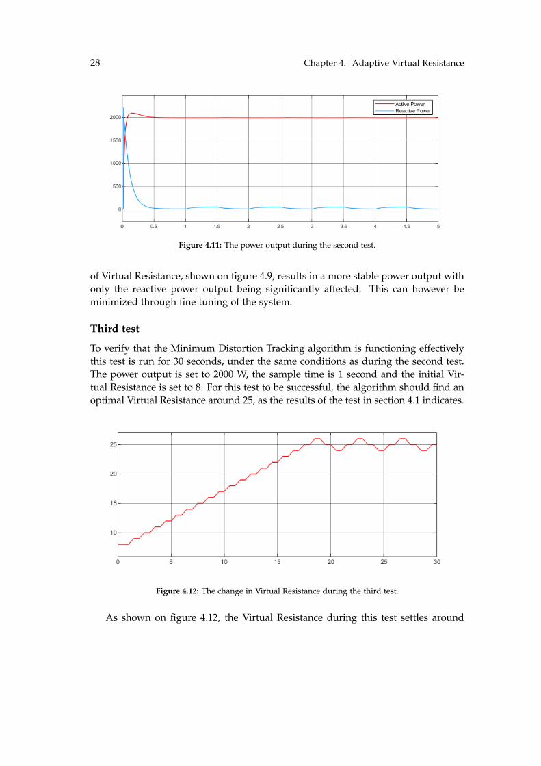
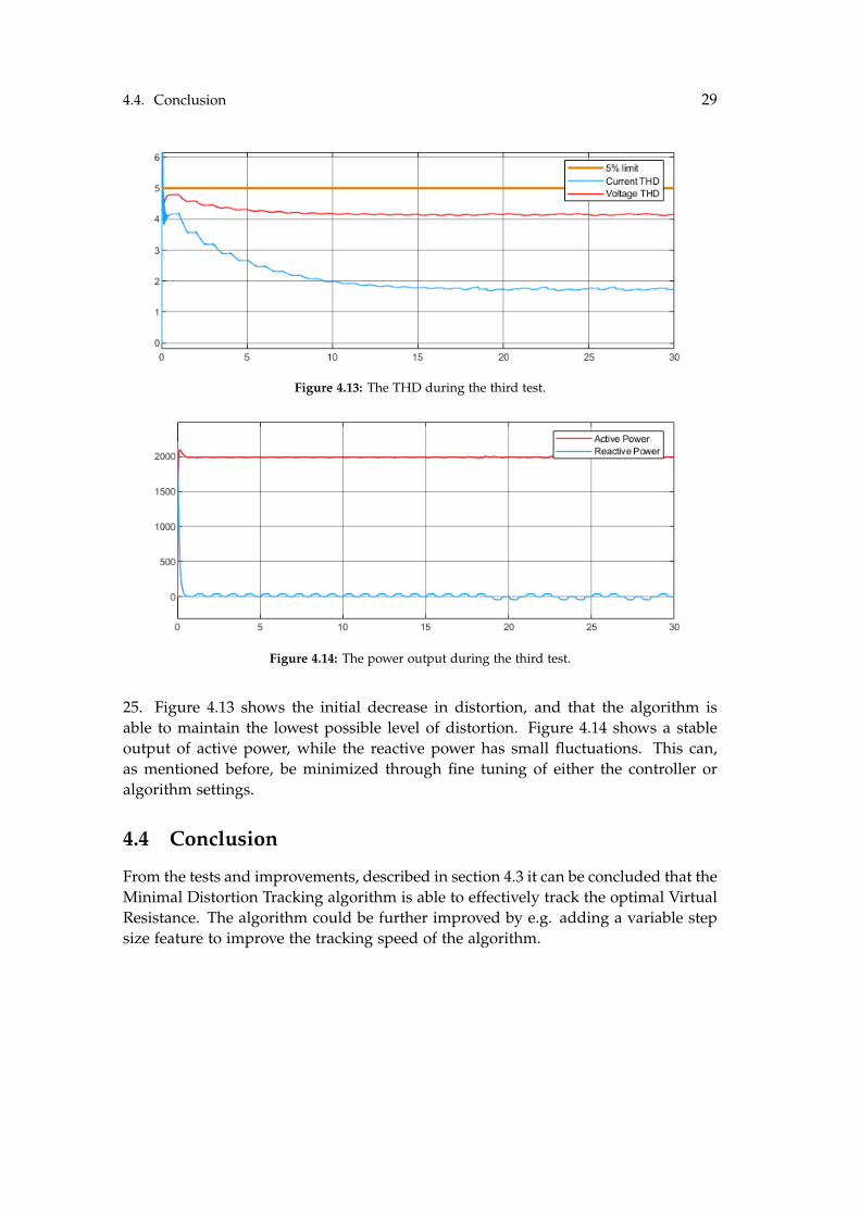
Third test
To verify that the Minimum Distortion Tracking algorithm is functioning effectivelythis test is run for 30 seconds, under the same conditions as during the second test.The power output is set to 2000 W, the sample time is 1 second and the initial Vir-tual Resistance is set to 8. For this test to be successful, the algorithm should find anoptimal Virtual Resistance around 25, as the results of the test in section 4.1 indicates.
Figure 4.12: The change in Virtual Resistance during the third test.
As shown on figure 4.12, the Virtual Resistance during this test settles around
4.4. Conclusion 29
Figure 4.13: The THD during the third test.
Figure 4.14: The power output during the third test.
25. Figure 4.13 shows the initial decrease in distortion, and that the algorithm isable to maintain the lowest possible level of distortion. Figure 4.14 shows a stableoutput of active power, while the reactive power has small fluctuations. This can,as mentioned before, be minimized through fine tuning of either the controller oralgorithm settings.
4.4 Conclusion
From the tests and improvements, described in section 4.3 it can be concluded that theMinimal Distortion Tracking algorithm is able to effectively track the optimal VirtualResistance. The algorithm could be further improved by e.g. adding a variable stepsize feature to improve the tracking speed of the algorithm.

Chapter 5
Lab Testing
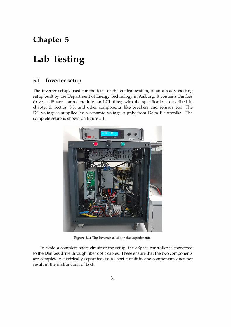
5.1 Inverter setup
The inverter setup, used for the tests of the control system, is an already existingsetup built by the Department of Energy Technology in Aalborg. It contains Danfossdrive, a dSpace control module, an LCL filter, with the specifications described inchapter 3, section 3.3, and other components like breakers and sensors etc. TheDC voltage is supplied by a separate voltage supply from Delta Elektronika. Thecomplete setup is shown on figure 5.1.
Figure 5.1: The inverter used for the experiments.
To avoid a complete short circuit of the setup, the dSpace controller is connectedto the Danfoss drive through fiber optic cables. These ensure that the two componentsare completely electrically separated, so a short circuit in one component, does notresult in the malfunction of both.
31
32 Chapter 5. Lab Testing
5.2 Implementation
The designed PI control system with Virtual Resistance has been implemented intoan already existing control system, designed for the specific inverter setup. The con-trol system, which was provided with the inverter setup, contains a PI controller withharmonic compensation for the 5th and 7th harmonic components. The system alsouses 3rd harmonic injection to further improve the performance of the control system.
The main disadvantage with the Virtual Resistor method is that it requires a dou-ble derivative, which, under normal circumstances, is sensitive to noisy measure-ments. To minimize this problem, a discrete time filtered derivative is used.
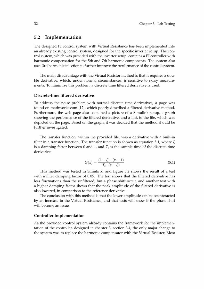
Discrete-time filtered derivative
To address the noise problem with normal discrete time derivatives, a page wasfound on mathworks.com [12], which poorly described a filtered derivative method.Furthermore, the web page also contained a picture of a Simulink setup, a graphshowing the performance of the filtered derivative, and a link to the file, which wasdepicted on the page. Based on the graph, it was decided that the method should befurther investigated.
The transfer function, within the provided file, was a derivative with a built-infilter in a transfer function. The transfer function is shown as equation 5.1, where ζ
is a damping factor between 0 and 1, and Ts is the sample time of the discrete-timederivative.
G(z) =(1 − ζ) · (z − 1)
Ts · (z − ζ)(5.1)
This method was tested in Simulink, and figure 5.2 shows the result of a testwith a filter damping factor of 0.85. The test shows that the filtered derivative hasless fluctuations than the unfiltered, but a phase shift occur, and another test witha higher damping factor shows that the peak amplitude of the filtered derivative isalso lowered, in comparison to the reference derivative.
The conclusion with this method is that the lower amplitude can be counteractedby an increase in the Virtual Resistance, and that tests will show if the phase shiftwill become an issue.
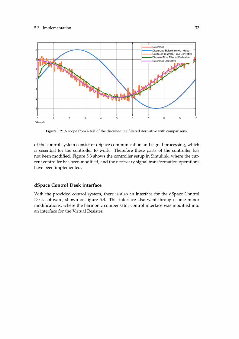
Controller implementation
As the provided control system already contains the framework for the implemen-tation of the controller, designed in chapter 3, section 3.4, the only major change tothe system was to replace the harmonic compensator with the Virtual Resister. Most
5.2. Implementation 33
Figure 5.2: A scope from a test of the discrete-time filtered derivative with comparisons.
of the control system consist of dSpace communication and signal processing, whichis essential for the controller to work. Therefore these parts of the controller hasnot been modified. Figure 5.3 shows the controller setup in Simulink, where the cur-rent controller has been modified, and the necessary signal transformation operationshave been implemented.
dSpace Control Desk interface
With the provided control system, there is also an interface for the dSpace ControlDesk software, shown on figure 5.4. This interface also went through some minormodifications, where the harmonic compensator control interface was modified intoan interface for the Virtual Resister.
34 Chapter 5. Lab Testing
Figure 5.3: The controller setup for the inverter, constructed in Simulink
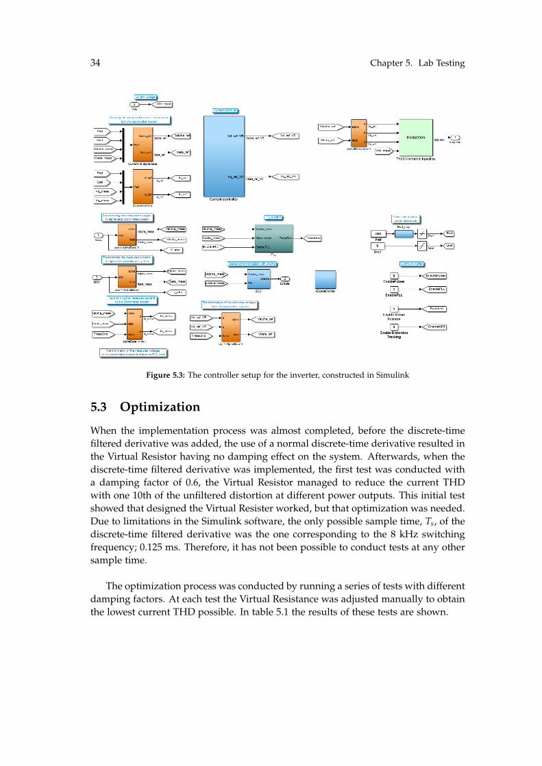
5.3 Optimization
When the implementation process was almost completed, before the discrete-timefiltered derivative was added, the use of a normal discrete-time derivative resulted inthe Virtual Resistor having no damping effect on the system. Afterwards, when thediscrete-time filtered derivative was implemented, the first test was conducted witha damping factor of 0.6, the Virtual Resistor managed to reduce the current THDwith one 10th of the unfiltered distortion at different power outputs. This initial testshowed that designed the Virtual Resister worked, but that optimization was needed.Due to limitations in the Simulink software, the only possible sample time, Ts, of thediscrete-time filtered derivative was the one corresponding to the 8 kHz switchingfrequency; 0.125 ms. Therefore, it has not been possible to conduct tests at any othersample time.
The optimization process was conducted by running a series of tests with differentdamping factors. At each test the Virtual Resistance was adjusted manually to obtainthe lowest current THD possible. In table 5.1 the results of these tests are shown.
5.3. Optimization 35
Figure 5.4: The modified inverter interface in dSpace ControlDesk.
Table 5.1: The results of the optimization tests
Test DFCurrent THD at Virtual Resistance at
500 W 1000 W 2000 W 500 W 1000 W 2000 W1 0.6 16.0 % 11.0 % 6.3 % 7 7 72 0.65 16.4 % 10.5 % 6.1 % 10 10 103 0.7 16.1 % 9.8 % 5.7 % 15 17 204 0.75 14.5 % 8.2 % 4.7 % 20 23 285 0.8 13.7 % 7.8 % 4.1 % 27 35 396 0.85 13.0 % 7.0 % 3.7 % 36 48 587 0.9 12.4 % 6.1 % 3.1 % 58 74 868 0.95 12.1 % 5.9 % 3.1 % 110 155 1659 0.99 13.1 % 6.8 % 3.5 % 650 840 800
Based on the results of the optimization, it can be concluded that the optimaldamping factor of this Virtual Resistor is within the range of 0.90 to 0.95. Further-more, in response to the concerns described under Discrete-time filtered derivativein section 5.2, it can be concluded that the phase shift in these filtered derivatives
36 Chapter 5. Lab Testing
did not have a significant effect on the efficiency of the Virtual Resistor. This mightbe due to the small sample time, but it was not, as mentioned before, possible totest otherwise with the current setup. It can also be concluded, that the decrease inamplitude of the filtered derivatives was counteracted by an increase in the VirtualResistance without amplifying remaining noise to a degree, that would cause desta-bilization.
Finally, the results confirm the assumption from chapter 4, section 4.1, that thedifference in optimal Virtual Resistance, at different operational conditions, wouldbe more significant under real conditions. Therefore, implementation of a MinimalDistortion Tracking algorithm could greatly enhance the performance of this invertercontrol system.
5.4 Validation test
In this section, the final validation experiment will be described, and results from thelab setup and simulation model will be compared. The experiment will consist of aseries of tests with varying reference power input. The optimal Virtual Resistance isobtained, in the lab through manual adjustment, and in the simulation by MinimalDistortion Tracking. For this experiment, the integration damping factor is set to 0.90,within the Virtual Resistance estimation in the lab setup.
Table 5.2: The results of the validation tests
TestReference power Lab. result Sim. resultActive Reactive VR THD VR THD
1 500 0 48 12.9 % 23 6.9 %2 500 500 72 10.8 % 17 6.0 %3 500 -500 76 8.5 % 27 4.0 %4 1000 0 74 6.2 % 24 3.5 %5 1000 500 68 6.5 % 17 3.9 %6 1000 1000 66 5.3 % 13 4.1 %7 1000 -500 64 5.5 % 27 2.6 %8 2000 0 92 2.5 % 25 1.7 %9 2000 500 70 4.2 % 18 2.2 %
10 2000 1000 62 3.5 % 14 2.9 %11 2000 -500 74 3.2 % 27 1.4 %12 2000 -1000 56 3.4 % 27 1.0 %
On table 5.2 the results show, that there is no apparent correlation between theoptimal Virtual Resistance in the tests, but a clear correlation between the THD re-sults. On figure 5.5, where the THD results from the simulations have been scaled up
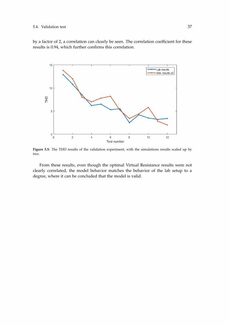
5.4. Validation test 37
by a factor of 2, a correlation can clearly be seen. The correlation coefficient for theseresults is 0.94, which further confirms this correlation.
Figure 5.5: The THD results of the validation experiment, with the simulations results scaled up bytwo.
From these results, even though the optimal Virtual Resistance results were notclearly correlated, the model behavior matches the behavior of the lab setup to adegree, where it can be concluded that the model is valid.

Discussion
First of all the choice of the Virtual Resistor over the PR controller and Notch filter wasbased on the fact, that the Virtual Resistor seemed more robust to external grid influ-ences. As this claim has not been tested, the truth of the claim will remain unknown.Furthermore, no literature was found with a definitive answer to, which method isthe best for grid-connected applications, as all the papers had slightly different ap-proaches, several only compared with standard approaches to competing methods,and some did not document the testing procedures as well as others. Most resultswere presented at graphs and scopes, and very few numbers were presented, whichfurther complicates the comparison. For future reference, these methods should betested head to head under similar conditions, with well documented testing proce-dures and with comparable results like THD or similar values.
Among the papers, presented in the review, few presented THD measurements,and of those only one was comparable to the best results, achieved during the test-ing phase, which would indicate that the experimental results, and thereby also theimplemented control system works to a satisfactory degree. The requirement of lessthan 5% THD was met in all the test at 2000 W, and the correlation between thepredicted and actual behavior of the system was satisfactory as well. The predictedTHDs was approximately half of the actual ones, which could be caused by some ofthe distortion, caused by the switching dynamics of the inverter, not being accountedfor in the model. Another reason could be the estimated grid impedance, which canbe difficult to estimate. These factors could account for most of the margin of error,but the overall model seems valid anyway.
The implementation of the PI controller and Virtual Resistor went well due to thefiltered discrete-time filtered derivative, which ensured that the double derivative ofthe Virtual Resistance worked despite noise in the measurements. This problem wasmentioned in many papers, but none of the papers seemed to use any method similarto this one. The test results showed that the method was effective, but if the resultsare compared to results from the 8th semester project in the appendix, where a two-loop controller with harmonic compensation was used, the results for all referencepower outputs, except the 2000 W test, had a smaller THD than the results in thesetests. This could indicate that the Virtual Resistance method works best under higherpower outputs.
Even though the concept of Adaptable Virtual Resistance was documented in onepaper, the approach with a Minimal Distortion Tracking algorithm seems very dif-ferent from the method, described in that paper. The Minimal Distortion Tracking
39

40 Chapter 5. Lab Testing
seems like a promising addition to the concept of Adaptable Virtual Resistance. Dueto time constraints and setup problems, the MDT algorithm was not implementedinto the lab. control system. The problem with the sample time, described in chapter5, section 5.3, also affected the implementation of the algorithm, as error messagesof asynchronous behavior kept occurring throughout the implementation attempts.This is, however, only a problem with the Matlab/Simulink environment, and nota problem with the algorithm itself, and it will therefore be possible to implementinto other environments, and maybe also Matlab/Simulink, if the right solution tothe problem is found.
However, even though the algorithm has not been implemented into the controllerof the lab setup, the mindset behind the algorithm suggests that it would work as in-tended, as the base algorithm has several similarities with the manual adjustment,used for the experiments.
The wider reaching effect of this, or any other, active damping method is, thatthe need for passive damping resistors is replaced by smarter control systems, andthereby the power losses and affiliated need for cooling of damping resistors is nolonger present. This will result in a more efficient and cost effective Voltage SourceInverters, which is highly desirable on a growing market for power electronic con-verters.

Conclusion
The overall conclusion of this project is that a PI control system with Virtual Re-sistance has been designed, tested and predominantly works as intended. The im-plementation of the designed control system and especially the Virtual Resistanceproved successful, by using discrete-time filtered derivatives to tackle the problem ofdouble derivatives and noisy measurements.
The Minimal Distortion Tracking algorithm has shown a potential to become agreat addition to the concept of Adaptable Virtual Resistance, even though it has yetto be properly tested on a real inverter control system.
41

Bibliography
[1] S. V. Araujo et al. “LCL filter design for grid-connected NPC inverters in off-shore wind turbines”. In: Proc. 7th Internatonal Conf. Power Electronics. Oct. 2007,pp. 1133–1138. doi: 10.1109/ICPE.2007.4692556.
[2] F. Blaabjerg et al. “Overview of Control and Grid Synchronization for Dis-tributed Power Generation Systems”. In: IEEE Transactions on Industrial Elec-tronics 53.5 (Oct. 2006), pp. 1398–1409. issn: 0278-0046. doi: 10.1109/TIE.2006.881997.
[3] S. Bosch, D. Lebsanft, and H. Steinhart. “Self-adaptive resonance frequencytracking for digital notch-filter-based active damping in LCL-filter-based activepower filters”. In: Proc. 19th European Conf. Power Electronics and Applications(EPE’17 ECCE Europe). Sept. 2017, P.1–P.10. doi: 10.23919/EPE17ECCEEurope.2017.8099104.
[4] M. Büyük et al. “A notch filter based active damping of llcl filter in shunt activepower filter”. In: Proc. Int. Symp. Power Electronics (Ee). Oct. 2017, pp. 1–6. doi:10.1109/PEE.2017.8171701.
[5] H. H. Figueira et al. “Brazilian grid-connected photovoltaic inverters standards:A comparison with IEC and IEEE”. In: Proc. IEEE 24th Int. Symp. IndustrialElectronics (ISIE). June 2015, pp. 1104–1109. doi: 10.1109/ISIE.2015.7281626.
[6] H. Ge et al. “Research on LCL filter active damping strategy in active powerfilter system”. In: Proc. Identification and Control (ICMIC) 2017 9th Int. Conf. Mod-elling. July 2017, pp. 476–481. doi: 10.1109/ICMIC.2017.8321691.
[7] W. Ghzaiel et al. “A novel grid impedance estimation technique based on adap-tive virtual resistance control loop applied to distributed generation inverters”.In: Proc. 15th European Conf. Power Electronics and Applications (EPE). Sept. 2013,pp. 1–10. doi: 10.1109/EPE.2013.6631966.
[8] IEEE Standard for Interconnection and Interoperability of Distributed Energy Re-sources with Associated Electric Power Systems Interfaces. IEEE Standards Asso-ciation, Apr. 2018. doi: 10.1109/IEEESTD.2018.8332112.
[9] K. Koiwa et al. “Sensorless virtual resistance damping method for grid-connected three-phase PWM converter with LCL filter”. In: Proc. Int. Conf. Elec-trical Machines and Systems (ICEMS). Oct. 2013, pp. 1746–1749. doi: 10.1109/ICEMS.2013.6713280.
[10] Y. Lei et al. “An improved virtual resistance damping method for grid-connected inverters with LCL filters”. In: Proc. IEEE Energy Conversion Congressand Exposition. Sept. 2011, pp. 3816–3822. doi: 10.1109/ECCE.2011.6064287.
[11] M. Liserre, F. Blaabjerg, and S. Hansen. “Design and control of an LCL-filter-based three-phase active rectifier”. In: IEEE Transactions on Industry Applications
43
44 Bibliography
41.5 (Sept. 2005), pp. 1281–1291. issn: 0093-9994. doi: 10.1109/TIA.2005.853373.
[12] MathWorks. Discrete-Time Derivative of Floating-Point Input. Last accessed: May2019. url: www . mathworks . com / help / simulink / slref / discrete - time -
derivative-of-floating-point-input.html.[13] Photovoltaic (PV) systems - Characteristics of the utility interface. International Elec-
trotechnical Commission, Dec. 2004. url: webstore . iec . ch / publication /
5736.[14] Power Electronics Sam Davis. Solar System Efficiency: Maximum Power
Point Tracking is Key. Last accessed: May 2019. Dec. 2015. url: www .
powerelectronics.com/solar/solar-system-efficiency-maximum-power-
point-tracking-key.[15] Hisham Hasan Taleb, Waqas Aslam Cheema, and Mikkel Rindholt. Power Con-
trol of Grid Connected Converter for Offshore Wind Power System. 8th semesterproject report - Found in appendix. June 2018.
[16] C. Tarasantisuk et al. “Active and reactive power control for three-phase gridinverters with proportional resonant control strategies”. In: Proc. Telecommu-nications and Information Technology (ECTI-CON) 2016 13th Int. Conf. ElectricalEngineering/Electronics, Computer. June 2016, pp. 1–6. doi: 10.1109/ECTICon.2016.7561379.
[17] R. Teodorescu et al. “Proportional-resonant controllers and filters for grid-connected voltage-source converters”. In: IEE Proceedings-Electric Power Appli-cations 153.5 (Sept. 2006), pp. 750–762. issn: 1350-2352. doi: 10.1049/ip-epa:20060008.
[18] T. C. Y. Wang et al. “Output filter design for a grid-interconnected three-phaseinverter”. In: Proc. PESC ’03. IEEE 34th Annual Conf. Power Electronics Specialist.Vol. 2. June 2003, 779–784 vol.2. doi: 10.1109/PESC.2003.1218154.
[19] Q. Zhao, F. Liang, and W. Li. “A new control scheme for LCL-type grid-connected inverter with a Notch filter”. In: Proc. 27th Chinese Control and De-cision Conf. (2015 CCDC). May 2015, pp. 4073–4077. doi: 10.1109/CCDC.2015.7162637.
[20] W. Zhao and G. Chen. “Comparison of active and passive damping methodsfor application in high power active power filter with LCL-filter”. In: Proc. Int.Conf. Sustainable Power Generation and Supply. Apr. 2009, pp. 1–6. doi: 10.1109/SUPERGEN.2009.5347992.
![LCL filter design for grid-connected inverters by ... · Different design procedures have been proposed in litera-ture for LCL filter based on frequency domain approach [9]– [14]](https://img.pdfslide.net/doc/110x75/5fce53dcdeb4f811cc7ea7db/lcl-filter-design-for-grid-connected-inverters-by-different-design-procedures.jpg)


![LCL-resonance damping strategies for grid-connected ...Filter-based AD improves stability by adding a digital filter next to the current controller [11–16]. For feedback-based AD,](https://img.pdfslide.net/doc/110x75/5f7d1e3417a65079300d223e/lcl-resonance-damping-strategies-for-grid-connected-filter-based-ad-improves.jpg)


![Conclusioni - GRIX.ITApp(1).pdf[8] M. Liserre, F. Blaabjerg, A. Dell’Aquila, “A stable three-phase LCL-filter based active rectifier without damping”, ISA 2003, Salt Lake City,](https://img.pdfslide.net/doc/110x75/60de65394e98c835477a202d/conclusioni-grixit-app1pdf-8-m-liserre-f-blaabjerg-a-dellaaquila.jpg)
![Aalborg Universitet Stability analysis and active damping for ......an LCL-filter or LLCL-filter, active damping [7-11] or passive damping [12-15] measures may be adopted. Passive](https://img.pdfslide.net/doc/110x75/60de630f7e12ee0ef01d287b/aalborg-universitet-stability-analysis-and-active-damping-for-an-lcl-filter.jpg)
![Resonance Damping and Parameter Design Method for LCL-LC ... · The filter can be of different types [6]. Compared with the first order L filter, the third-order LCL filter can meet](https://img.pdfslide.net/doc/110x75/5e76b9e50c589625166846e9/resonance-damping-and-parameter-design-method-for-lcl-lc-the-filter-can-be-of.jpg)