Embed Size (px)
Citation preview
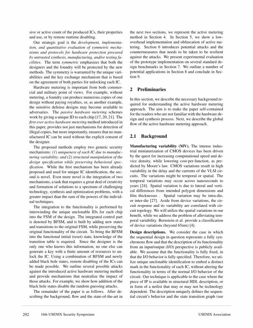
Active Hardware Metering for Intellectual PropertyProtection and Security
Yousra M. AlkabaniComputer Science Dept.
Rice University, Houston, [email protected]
Farinaz KoushanfarElectrical and Computer Engineering Dept.
Rice University, Houston, [email protected]
Abstract
We introduce the first active hardware metering schemethat aims to protect integrated circuits (IC) intellectualproperty (IP) against piracy and runtime tampering. Thenovel metering method simultaneously employs inherentunclonable variability in modern manufacturing tech-nology, and functionality preserving alternations of thestructural IC specifications. Active metering works byenabling the designers to lock each IC and to remotelydisable it. The objectives are realized by adding newstates and transitions to the original finite state machine(FSM) to create boosted finite state machines(BFSM) ofthe pertinent design. A unique and unpredictable ID gen-erated by an IC is utilized to place an BFSM into thepower-up state upon activation. The designer, knowingthe transition table, is the only one who can generate in-put sequences required to bring the BFSM into the func-tional initial (reset) state. To facilitate remote disablingof ICs, black hole states are integrated within the BFSM.
We introduce nine types of potential attacks againstthe proposed active metering method. We further de-scribe a number of countermeasures that must be takento preserve the security of active metering against the po-tential attacks. The implementation details of the methodwith the objectives of being low-overhead, unclonable,obfuscated, stable, while having a diverse set of keysis presented. The active metering method was imple-mented, synthesized and mapped on the standard bench-mark circuits. Experimental evaluations illustrate thatthe method has a low-overhead in terms of power, de-lay, and area, while it is extremely resilient against theconsidered attacks.
1 Introduction
In the dominant horizontal semiconductor businessmodel, piracy (illegal copying) and tampering of hard-ware are omnipresent. In the horizontal business model,
hardware IP1 designed by the leading edge designersare mostly manufactured in untrusted offshore countrieswith lower labor and operational cost. This places thedesigners in an unusual asymmetric relationship: the de-signed IP is transparent to the manufacturers, but thefabrication process, quantity and added circuitry to themanufactured integrated circuits (ICs) by the foundry areclandestine to the designers and IP providers.
The security threat, financial loss and economic im-pacts of hardware piracy which have received far lessattention compared to software, is even more dramaticthan software [8, 31]. Software piracy has received moreattention compared to hardware also because it requireslow-cost resources that are available to the general pub-lic. Protection of hardware is also crucially importantbecause the ICs are pervasively used in almost all elec-tronic devices and the potentially adversarial fabricationhouse has the full control over the hardware resourcesbeing manufactured. It is estimated that the computerhardware, computer peripherals, and embedded systemsare the dominant pirated IP components [31].
Several other issues make the IC protection problemstruly challenging: (i) very little is known about the cur-rent and potential IC tampering attacks; (ii) numerousattacking strategies exist, since tampering can be con-ducted at many levels of abstraction of the synthesis pro-cess; (iii) the most likely hardware adversaries are fi-nancially strong foundries and foreign governments withlarge economic resources and technological expertise;(iv) the adversary has full access to the structural specifi-cation of the design and most often also to the manufac-turing test vectors; (v) the internal part of manufacturedICs are intrinsically opaque. While it is possible to to-mographically scan an IC, the dense metal interconnectin 8 or more layers of modern manufacturing technol-ogy greatly reduce the effectiveness of such expensiveinspections.
IC metering is a set of security protocols that enablethe design house to gain post-fabrication control by pas-
16th USENIX Security SymposiumUSENIX Association 291
sive or active count of the produced ICs, their propertiesand use, or by remote runtime disabling.
Our strategic goal is the development, implementa-tion, and quantitative evaluation of symmetric mecha-nisms and protocols for hardware protection procuredby untrusted synthesis, manufacturing, and/or testing fa-cilities. The term symmetric emphasizes that both thedesigners and the foundry will be protected by the newmethods. The symmetry is warranted by the unique vari-abilities and the key exchange mechanism that is basedon the agreement of both parties for unlocking each IC.
Hardware metering is important from both commer-cial and military point of views. For example, withoutmetering, a foundry can produce numerous copies of onedesign without paying royalties, or, as another example,the sensitive defense designs may become available toadversaries. The passive hardware metering schemeswork by giving a unique ID to each chip [17, 20, 21]. Thefirst ever active hardware metering method introduced inthis paper, provides not just mechanisms for detection ofillegal copies, but more importantly, ensures that no man-ufactured IC can be used without the explicit consent ofthe designer.
The proposed methods employ two generic securitymechanisms: (1) uniqueness of each IC due to manufac-turing variability; and (2) structural manipulation of thedesign specification while preserving behavioral spec-ification. While the first mechanism has been alreadyproposed and used for unique IC identification, the sec-ond is novel. Even more novel is the integration of twomechanisms, a task that requires a great deal of creativityand formation of solutions to a spectrum of challengingtechnology, synthesis and optimization problems, with agreater impact than the sum of the powers of the individ-ual techniques.
The integration to the functionality is performed byinterwinding the unique unclonable IDs for each chipinto the FSM of the design. The integrated control partis denoted by BFSM, and is built by adding new statesand transitions to the original FSM, while preserving theoriginal functionality of the circuit. To bring the BFSMinto the functional initial (reset) state, knowledge of thetransition table is required. Since the designer is theonly one who knows this information, no one else cangenerate a key with a finite amount of resources to un-lock the IC. Using a combination of BFSM and newlyadded black hole states, remote disabling of the ICs canbe made possible. We outline several possible attacksagainst the introduced active hardware metering methodand provide mechanisms that neutralize the impact ofthose attacks. For example, we show how addition of theblack hole states disable the random guessing attacks.
The remainder of the paper is as follows. After de-scribing the background, flow and the state-of-the-art in
the next two sections, we represent the active meteringmethod in Section 4. In Section 5, we show a low-overhead implementation and obfuscation of active me-tering. Section 6 introduces potential attacks and thecountermeasures that needs to be taken to be resilientagainst the attacks. We present experimental evaluationof the prototype implementation on several standard de-sign benchmarks in Section 7. We outline a number ofpotential applications in Section 8 and conclude in Sec-tion 9.
2 Preliminaries
In this section, we describe the necessary background re-quired for understanding the active hardware meteringapproach. The aim is to make the paper self-containedfor the readers who are not familiar with the hardware de-sign and synthesis process. Next, we describe the globalflow of the active hardware metering approach.
2.1 Background
Manufacturing variability (MV). The intense indus-trial miniaturization of CMOS devices has been drivenby the quest for increasing computational speed and de-vice density, while lowering cost-per-function, as pre-dicted by Moore’s law. CMOS variations result in highvariability in the delay and the currents of the VLSI cir-cuits. The variations might be temporal or spatial. Thetemporal variations may occur across nanoseconds toyears [24]. Spatial variation is due to lateral and verti-cal differences from intended polygon dimensions andfilm thicknesses . Spatial variation may be intra-die,or inter-die [27]. Aside from device variations, the cir-cuit response and its variability are correlated with cir-cuit topology. We will utilize the spatial variations in ourbenefit, while we address the problem of alleviating tem-poral variability. Bernstein et al. provide a classificationof device variations (beyond 65nm) [4].
Design descriptions. We consider the case in whichthe sequential design in question represents a fully syn-chronous flow and that the description of its functionalityfrom an input/output (I/O) perspective is publicly avail-able. We assume that the functionality is fully fixed, inthat the I/O behavior is fully specified. Therefore, we uti-lize unique unclonable identification to embed a distinctmark in the functionality of each IC, without altering thefunctionality in terms of the normal I/O behavior of thecircuit. Our technique is applicable to the case where thepiece of IP is available in structural HDL description, orin form of a netlist that may or may not be technologydependent. The description uniquely defines the sequen-tial circuit’s behavior and the state transition graph (see
16th USENIX Security Symposium USENIX Association292
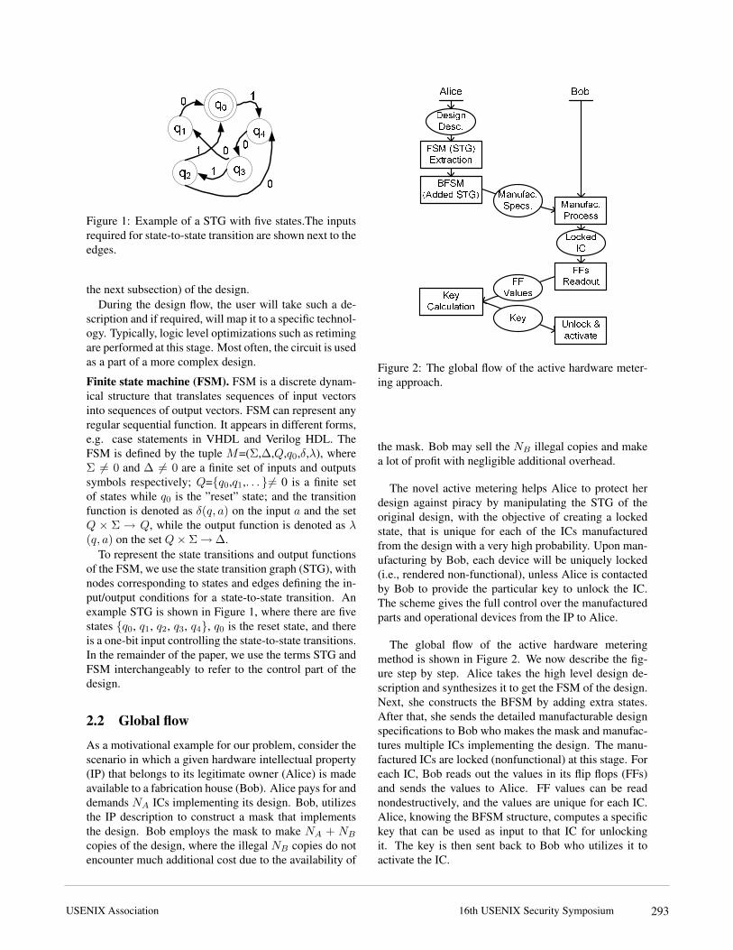
q2 q4q3q1 q00 11 0001Figure 1: Example of a STG with five states.The inputsrequired for state-to-state transition are shown next to theedges.
the next subsection) of the design.During the design flow, the user will take such a de-
scription and if required, will map it to a specific technol-ogy. Typically, logic level optimizations such as retimingare performed at this stage. Most often, the circuit is usedas a part of a more complex design.
Finite state machine (FSM). FSM is a discrete dynam-ical structure that translates sequences of input vectorsinto sequences of output vectors. FSM can represent anyregular sequential function. It appears in different forms,e.g. case statements in VHDL and Verilog HDL. TheFSM is defined by the tuple M=(Σ,∆,Q,q0,δ,λ), whereΣ 6= 0 and ∆ 6= 0 are a finite set of inputs and outputssymbols respectively; Q={q0,q1,. . . }6= 0 is a finite setof states while q0 is the ”reset” state; and the transitionfunction is denoted as δ(q, a) on the input a and the setQ × Σ → Q, while the output function is denoted as λ(q, a) on the set Q × Σ → ∆.
To represent the state transitions and output functionsof the FSM, we use the state transition graph (STG), withnodes corresponding to states and edges defining the in-put/output conditions for a state-to-state transition. Anexample STG is shown in Figure 1, where there are fivestates {q0, q1, q2, q3, q4}, q0 is the reset state, and thereis a one-bit input controlling the state-to-state transitions.In the remainder of the paper, we use the terms STG andFSM interchangeably to refer to the control part of thedesign.
2.2 Global flow
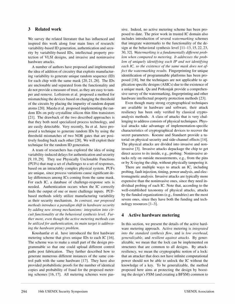
As a motivational example for our problem, consider thescenario in which a given hardware intellectual property(IP) that belongs to its legitimate owner (Alice) is madeavailable to a fabrication house (Bob). Alice pays for anddemands NA ICs implementing its design. Bob, utilizesthe IP description to construct a mask that implementsthe design. Bob employs the mask to make NA + NB
copies of the design, where the illegal NB copies do notencounter much additional cost due to the availability of
Alice BobDesign Desc.FSM (STG)ExtractionBFSM (Added STG) Locked ICKey Calculation Unlock & activateManufac.Specs.FF ValuesKey FFs Readout Manufac.Process
Figure 2: The global flow of the active hardware meter-ing approach.
the mask. Bob may sell the NB illegal copies and makea lot of profit with negligible additional overhead.
The novel active metering helps Alice to protect herdesign against piracy by manipulating the STG of theoriginal design, with the objective of creating a lockedstate, that is unique for each of the ICs manufacturedfrom the design with a very high probability. Upon man-ufacturing by Bob, each device will be uniquely locked(i.e., rendered non-functional), unless Alice is contactedby Bob to provide the particular key to unlock the IC.The scheme gives the full control over the manufacturedparts and operational devices from the IP to Alice.
The global flow of the active hardware meteringmethod is shown in Figure 2. We now describe the fig-ure step by step. Alice takes the high level design de-scription and synthesizes it to get the FSM of the design.Next, she constructs the BFSM by adding extra states.After that, she sends the detailed manufacturable designspecifications to Bob who makes the mask and manufac-tures multiple ICs implementing the design. The manu-factured ICs are locked (nonfunctional) at this stage. Foreach IC, Bob reads out the values in its flip flops (FFs)and sends the values to Alice. FF values can be readnondestructively, and the values are unique for each IC.Alice, knowing the BFSM structure, computes a specifickey that can be used as input to that IC for unlockingit. The key is then sent back to Bob who utilizes it toactivate the IC.
16th USENIX Security SymposiumUSENIX Association 293
3 Related work
We survey the related literature that has influenced andinspired this work along four main lines of research:variability-based ID generation, authentication and secu-rity by variability-based IDs, intellectual property pro-tection of VLSI designs, and invasive and noninvasivehardware attacks.
A number of authors have proposed and implementedthe idea of addition of circuitry that exploits manufactur-ing variability to generate unique random sequence (ID)for each chip with the same mask [20, 21, 28]. The IDsare unclonable and separated from the functionality anddo not provide a measure of trust, as they are easy to tam-per and remove. Loftstrom et al. proposed a method formismatching the devices based on changing the thresholdof the circuits by placing the impurity of random dopantatoms [20]. Maeda et al. proposed implementing the ran-dom IDs on poly-crystalline silicon thin film transistors[21]. The drawback of the two described approaches isthat they both need specialized process technology, andare easily detectable. Very recently, Su et al. have pro-posed a technique to generate random IDs by using thethreshold mismatches of two NOR gates that are posi-tively feeding back each other [28]. We will exploit theirtechnique for the random ID generation.
A team of researchers has explored the idea of usingvariability-induced delays for authentication and security[9, 19, 29]. They use Physically Unclonable Functions(PUFs) that map a set of challenges to a set of responses,based on an intractably complex physical system. PUFsare unique, since process variations cause significant de-lay differences among ICs coming from the same mask.For each IC, a database of challenge-response sets isneeded. Authentication occurs when the IC correctlyfinds the output of one or more challenge inputs. PUF-based methods solely utilize manufacturing variabilityas their security mechanism. In contrast, our proposedmethods introduce a paradigm shift in hardware securityby adding new strong mechanisms: integration into cir-cuit functionality at the behavioral synthesis level. Fur-ther more, even though the active metering methods canbe utilized for authentication, its main target is address-ing the hardware piracy problem.
Koushanfar et al. have introduced the first hardwaremetering scheme that gives unique IDs to each IC [16].The scheme was to make a small part of the design pro-grammable so that one could upload different controlpaths post fabrication. They further described how togenerate numerous different instances of the same con-trol path with the same hardware [17]. They have alsoprovided probabilistic proofs for the number of identicalcopies and probability of fraud for the proposed meter-ing schemes [16, 17]. All metering schemes were pas-
sive. Indeed, no active metering scheme has been pro-posed to date. The prior work in trusted IC domain alsoincludes introduction of several watermarking schemesthat integrate watermarks to the functionality of the de-sign at the behavioral synthesis level [11–13, 15, 22, 23,30, 32]. Watermarking is a fundamentally different prob-lem when compared to metering. It addresses the prob-lem of uniquely identifying each IP and not identifyingeach IC, so the existence of the same mask does not af-fect the watermarking results. Fingerprinting for uniqueidentification of programmable platforms has been pro-posed [18], but the techniques are not applicable to ap-plication specific designs (ASICs) due to the existence ofa unique mask. Qu and Potkonjak provide a comprehen-sive survey of the watermarking, fingerprinting and otherhardware intellectual property protection methods [23].
Even though many strong cryptographical techniquesare available in hardware and software, their attackresiliency has been only verified by classical crypto-analysis methods. A class of attacks that is very chal-lenging to address consists of physical techniques. Phys-ical attacks take advantage of implementation-specificcharacteristics of cryptographical devices to recover thesecret parameters. Koeune and Standaert provide a tu-torial on physical security and side-channel effects [14].The physical attacks are divided into invasive and non-invasive [3]. Invasive attacks depackage the chip to getdirect access to its inside, e.g., probing. Noninvasive at-tacks rely on outside measurements, e.g., from the pinsor by X-raying the chip, without physically tampering it.
There are multiple ways to attack an IC, includingprobing, fault injection, timing, power analysis, and elec-tromagnetic analysis. Invasive attacks are typically moreexpensive than the noninvasive ones, since they need in-dividual probing of each IC. Note that, according to thewell-established taxonomy of physical attacks, attacksby the funded organizations (e.g., foundries) are the mostsevere ones, since they have both the funding and tech-nology resources [1–3].
4 Active hardware metering
In this section, we present the details of the active hard-ware metering approach. Active metering is integratedinto the standard synthesis flow, and is low overhead,generalizable, and resilient against attacks. By gener-alizable, we mean that the lock can be implemented onstructures that are common to all designs. By attack-resiliency, we mean the cryptographic notion of a lock:that an attacker that does not have infinite computationalpower should not be able to unlock the IC without theknowledge of a key. To be generalizable, the methodproposed here aims at protecting the design by boost-ing the design’s FSM (and creating a BFSM) common to
16th USENIX Security Symposium USENIX Association294
the widely used class of sequential designs. In this sec-tion, we describe the BFSM construction and introducethe locking mechanism. Implementation details are dis-cussed in the next section.
4.1 Method
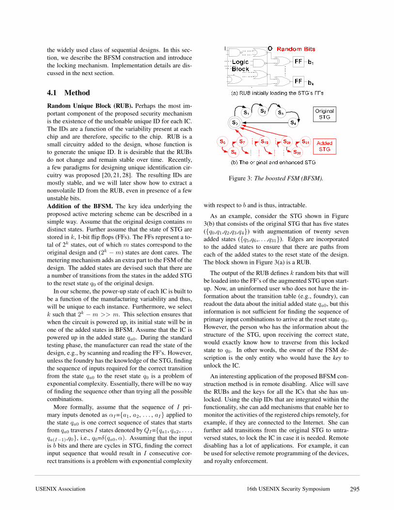
Random Unique Block (RUB). Perhaps the most im-portant component of the proposed security mechanismis the existence of the unclonable unique ID for each IC.The IDs are a function of the variability present at eachchip and are therefore, specific to the chip. RUB is asmall circuitry added to the design, whose function isto generate the unique ID. It is desirable that the RUBsdo not change and remain stable over time. Recently,a few paradigms for designing unique identification cir-cuitry was proposed [20, 21, 28]. The resulting IDs aremostly stable, and we will later show how to extract anonvolatile ID from the RUB, even in presence of a fewunstable bits.Addition of the BFSM. The key idea underlying theproposed active metering scheme can be described in asimple way. Assume that the original design contains mdistinct states. Further assume that the state of STG arestored in k, 1-bit flip flops (FFs). The FFs represent a to-tal of 2k states, out of which m states correspond to theoriginal design and (2k − m) states are dont cares. Themetering mechanism adds an extra part to the FSM of thedesign. The added states are devised such that there area number of transitions from the states in the added STGto the reset state q0 of the original design.
In our scheme, the power-up state of each IC is built tobe a function of the manufacturing variability and thus,will be unique to each instance. Furthermore, we selectk such that 2k − m >> m. This selection ensures thatwhen the circuit is powered up, its initial state will be inone of the added states in BFSM. Assume that the IC ispowered up in the added state qa0. During the standardtesting phase, the manufacturer can read the state of thedesign, e.g., by scanning and reading the FF’s. However,unless the foundry has the knowledge of the STG, findingthe sequence of inputs required for the correct transitionfrom the state qa0 to the reset state q0 is a problem ofexponential complexity. Essentially, there will be no wayof finding the sequence other than trying all the possiblecombinations.
More formally, assume that the sequence of I pri-mary inputs denoted as αI={a1, a2, . . . , aI} applied tothe state qa0 is one correct sequence of states that startsfrom qa0 traverses I states denoted by QI={qa1, qa2, . . . ,qa(I−1),q0}, i.e., q0=δ(qa0, α). Assuming that the inputis b bits and there are cycles in STG, finding the correctinput sequence that would result in I consecutive cor-rect transitions is a problem with exponential complexity
…….…….…….………...…….Logic Block……. Random Bits…….……. FF………... FFI O b1bkS1 S4S2 S3S0S5 S6 S7 S31S29 S30S15….…. …. ….…. …. Original STGAdded STG(a) RUB initially loading the STG’s FFs(b) The original and enhanced STG
Figure 3: The boosted FSM (BFSM).
with respect to b and is thus, intractable.
As an example, consider the STG shown in Figure3(b) that consists of the original STG that has five states({q0,q1,q2,q3,q4}) with augmentation of twenty sevenadded states ({q5,q6,. . . ,q31}). Edges are incorporatedto the added states to ensure that there are paths fromeach of the added states to the reset state of the design.The block shown in Figure 3(a) is a RUB.
The output of the RUB defines k random bits that willbe loaded into the FF’s of the augmented STG upon start-up. Now, an uninformed user who does not have the in-formation about the transition table (e.g., foundry), canreadout the data about the initial added state qa0, but thisinformation is not sufficient for finding the sequence ofprimary input combinations to arrive at the reset state q0.However, the person who has the information about thestructure of the STG, upon receiving the correct state,would exactly know how to traverse from this lockedstate to q0. In other words, the owner of the FSM de-scription is the only entity who would have the key tounlock the IC.
An interesting application of the proposed BFSM con-struction method is in remote disabling. Alice will savethe RUBs and the keys for all the ICs that she has un-locked. Using the chip IDs that are integrated within thefunctionality, she can add mechanisms that enable her tomonitor the activities of the registered chips remotely, forexample, if they are connected to the Internet. She canfurther add transitions from the original STG to untra-versed states, to lock the IC in case it is needed. Remotedisabling has a lot of applications. For example, it canbe used for selective remote programming of the devices,and royalty enforcement.
16th USENIX Security SymposiumUSENIX Association 295
4.2 Ensuring proper operation
The following issues and observations ensure proper op-eration and low-overhead of active hw metering:
(i) Storing the input sequence (key) for traversal tothe initial state q0. During testing, once Bob scans outthe FF values and sends them to Alice, she provides thekey to Bob. He includes both the original RUB and thekey in the chip, for example, in a nonvolatile memory.This data is utilized along with the unclonable RUB cir-cuit, for transition to the reset state. Since the power-upstate is unique for each IC, sequence of inputs (key) thattraverse the power-up state to the reset state is also spe-cific to each IC. One needs to store the key which per-forms the traversal at the power-up state on each chip.There are many ways to accomplish this. For exam-ple, the designer could add a small programmable partto the design which needs to be coded with the uniquesequence (key) before each IC is in operation. Codingensures protection of keys against other software attacks.As an alternative, the sequence might not be included inthe memory and just used as a permanent password tothe IC.
(ii) Powering up in one of the added states. Thiscondition can be easily guaranteed by selecting a largeenough k. Assuming that all the states have an equalprobability, the probability of starting in one of the addedstates is (2k − m)/2k. For a given m, we select k suchthat the probability of not being in one of the added statesis smaller than a given probability. For example, form = 100 and k = 30, the probability of starting upin an original state is less than 10−7.
(iii) Diversity of power-up states (unique IDs). kshould also be selected so that the probability of two ICshaving the same ID becomes very low. Assume that weneed to have d distinct ICs each with a unique ID. As-suming that the IDs are completely random and indepen-dent, we utilize the Birthday paradox to calculate thisprobability and to make it low. Consider the probabil-ity PICID(k, d) that no two ICs out of a group of d willhave matching IDs out of 2k equally possible IDs. Startwith an arbitrary chip’s ID. The probability that the sec-ond chip’s ID is different is (2k − 1)/2k. Similarly, theprobability that the third IC’s ID is different from the firsttwo is [(2k−1)/2k].[(2k−2)/2k]. The same computationcan be extended through the 2k-th ID. More formally,
PICID(k, d) =2k − 1
2k.2k − 2
2k. . . . .
2k − (d − 1)2k
=2k!
(2k − d)!2dk(1)
Thus, knowing d, the number of required distinct copies,
and setting a low value for PICID, we would be able tofind k that satisfies the above equation.
(iv) Overhead of the added STG. The number of statesincreases exponentially with adding each new bit, andthus, the scheme has a very low overhead. Note that,in modern designs, the control path of the design (i.e.,FSM) is less than 1% of the total area and hence, addinga small overhead to the FSM does not significantly affectthe total area [7, 10]. In the next section, we will describea low-overhead implementation of the proposed method.
(v) Diversity of keys. There is a need to ensure that thekeys are distinct in all parts of their sequences, or there isa very small shared subsequence between different keys.This is granted by making multiple paths on the graphfrom each of the states to the reset state. We will elabo-rate more on this issue in the attack resiliency section.
5 Low overhead implementation and ob-fuscation
In this section, we discuss the implementation details ofthe RUB and the BFSM that are the required buildingblocks for the active hardware metering approach. Westart by outlining the desired properties of each block,and then we delve into its implementation details.
5.1 RUB implementation
A critical aspect of the proposed security and protectionmechanisms is the generation of random ID bits. Thereare a number of properties that the RUB implementationhas to satisfy, including:
• Low overhead. The added parts must not introduce asignificant additional overhead in terms of delay, powerconsumption and the area.
• Distribution of IDs and their correlations. To havethe maximal difference between any two ID numbers (themaximal Hamming distances) the ID bits must be com-pletely random. Thus, no correlation must be presentamong the ID bits on the same die or across various dies.
• Indiscernibility. The IDs must be integrated within thedesign, such that they cannot be discerned by studyingthe layout of the circuit. For example, the IDs should notbe placed in a memory-like array, where the regularity ofthe array and its connections to the FFs could be easilydetected.
• Stability. There is a need to stabilize the IDs overthe lifetime of an IC. This is particularly important sincestudies have shown the temporal changes in CMOS pro-cess variations due to many environmental and aging ef-
16th USENIX Security Symposium USENIX Association296
fects including, residual charges, self-heating, negative-bias temperature instability, and hot electron effects [4].
For implementing the random IDs, we employed therecent novel approach proposed by Su et al. [28]. Theyhave designed and tested a new CMOS random ID gen-eration circuit that relies on digital latch threshold offsetvoltages. Using cross coupling of gates, they report sig-nificant improvement in readout speed and power con-sumption over the existing designs.
Each ID bit is generated by cross-coupled NOR gates.The latch sides are pulled low initially. At the high tolow clock transition, the state of each latch is determinedby the threshold voltage mismatch of the transistors. Es-sentially, the approach relies on the positive feedback in-herent in the latch configuration to amplify the mismatch.This design removes the need for comparators, low offsetamplifiers, or extra dopants needed in previous randomID generation methods [9, 20]. The nominal overheadof the above proposed approach is two NOR gates perbit. The authors have reported 96% stable IDs using thismethod, while using dummy latches to protect the IDs.
Even though we use the random bit architecture de-scribed above, our layout and implementation of randombits are very different. To be indiscernible, we do notplace the coupled NOR gates in an array, and instead syn-thesize them with the rest of the circuit and camouflagethem within the sea of gates. based on invariability of theID bits for an IC. In Subsection 6.2, we provide a mech-anism that ensures the occasional errors in ID bits do notaffect the hardware metering approach.
5.2 BFSM implementation
The key design objectives and challenges of the BFSMare as follows:
• Low overhead. The addition of the states to the orig-inal FSM must have a low overhead in terms of area,power, and delay. This is particularly challenging: aswe have computed in Subsection 4.2, even under the as-sumption of having RUBs with Uniform distribution ofrandom bits, the number of added states must be expo-nentially high to ensure a proper operation.
• Traversal path. There must be a path on the BFSM,from each of the power-up states (except for the blackhole states that we will describe in Section 6.2) to thereset state.
• States obfuscation. The states must be completely ob-fuscated and interchanged to camouflage the added STGand the original STG. Another level of obfuscation is dis-abling the observability of the FFs, so that similar stateson two ICs do not exactly have the same code scannedout from their FFs.
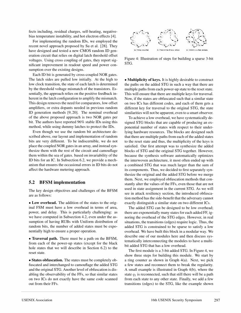
q3 q1q2q4 q0q5q6 q7 q3 q1q2q4 q0q5q6 q7 q3 q1q2q4 q0q5q6 q7(a) Ring counter (b) Reconnecting a state (c) Adding a few edgesFigure 4: Illustration of steps for building a sparse 3-bitSTG.
• Multiplicity of keys. It is highly desirable to constructthe paths on the added STG in such a way that there aremultiple paths from each power-up state to the reset state.This will ensure that there are multiple keys for traversal.Now, if the states are obfuscated such that a similar stateon two ICs has different codes, and each of them gets adifferent key for traversal to the original STG, the statesimilarities will not be apparent, even to a smart observer.
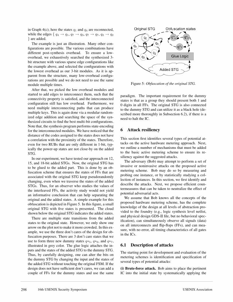
To achieve a low overhead, we have systematically de-signed STG blocks that are capable of producing an ex-ponential number of states with respect to their under-lying hardware resources. The blocks are designed suchthat there are multiple paths from each of the added statesto the reset state and thus, the multiplicity of the keys issatisfied. Our first attempt was to synthesize the addedblocks of STG and the original STG together. However,because the synthesis software automatically optimizesthe interwoven architecture, it most often ended up witha combined STG that was much larger than the sum ofits components. Thus, we decided to first separately syn-thesize the original and the added STG before we mergethem. Next, we employed obfuscation methods that con-stantly alter the values of the FFs, even those that are notused in state assignment in the current STG. As we willsee in attack resiliency section, the introduced obfusca-tion method has the side-benefit that the adversary cannotexactly distinguish a similar state on two different ICs.
The added STG can be designed to be low overhead;there are exponentially many states for each added FF, ig-noring the overhead of the STG edges. However, in realsituations, the transitions (edges) require logic. Thus, theadded STG is constrained to be sparse to satisfy a lowoverhead. We have built this block in a modular way. Wedescribe one of our modules here and then discuss sys-tematically interconnecting the modules to have a multi-bit added STG that has a low overhead.
The first module is a 3-bit added STG. In Figure 4, weshow three steps for building this module. We start bya ring counter as shown in Graph 4(a). Next, we picka few states and reconnect them to break the regularity.A small example is illustrated in Graph 4(b), where thestate q1 is reconnected, such that still there will be a pathfrom each state to any other state. Finally, we add a fewtransitions (edges) to the STG, like the example shown
16th USENIX Security SymposiumUSENIX Association 297
in Graph 4(c); here the states q1 and q4 are reconnected,while the edges { q4 → q1, q7 → q3, q7 → q7, q2 → q2
} are added.The example is just an illustration. Many other con-
figurations are possible. The various combinations havedifferent post-synthesis overhead. To ensure a low-overhead, we exhaustively searched the synthesized 3-bit structure with various sparse edge configurations likethe example above, and selected the configurations withthe lowest overhead as our 3-bit modules. As it is ap-parent from the structure, many low-overhead configu-rations are possible and we do not need to use the samemodule multiple times.
After that, we picked the low overhead modules andstarted to add edges to interconnect them, such that theconnectivity property is satisfied, and the interconnectedconfiguration still has low overhead. Furthermore, weneed multiple interconnecting paths that can producemultiple keys. This is again done via a modular random-ized edge addition and searching the space of the syn-thesized circuits to find the best multi-bit configurations.Note that, the synthesis program performs state-encodingfor the interconnected modules. We have noticed that thedistance of the codes assigned to the states does not havea correlation with the proximity of the states. Therefore,even for two RUBs that are only different in 1-bit, typ-ically the power-up states are not close-by on the addedSTG.
In our experiment, we have tested our approach on 12,15, and 18-bit added STGs. Now, the original STG hasto be glued to the added part. This is done by an ob-fuscation scheme that ensures the states of FFs that areassociated with the original STG keep pseudorandomlychanging, even when we traverse the states of the addedSTGs. Thus, for an observer who studies the values ofthe interleaved FFs, the activity study would not yieldan informative conclusion that can help separating theoriginal and the added states. A simple example for thisobfuscation is depicted in Figure 5. In this figure, a smalloriginal STG with five states is presented. The cloudshown below the original STG indicates the added states.
There are multiple state transitions from the addedstates to the original state. However, we only show onearrow on the plot not to make it more crowded. In this ex-ample, we use the three don’t cares of the design for ob-fuscation purposes. There are 3 don’t care states that weuse to form three new dummy states q∗5, q∗6, and q∗7,illustrated in grey color. The glue logic attaches the in-puts and the states of the added STG to the dummy STG.Thus, by carefully designing, one can alter the bits onthe dummy STG by changing the input and the states ofthe added STG without touching the original FSM. If thedesign does not have sufficient don’t cares, we can add acouple of FFs for the dummy states and use the same
q3 q1q2q0q4 q*5 q*6q*7Glue LogicOriginal STG Obfuscation states
Added STGFigure 5: Obfuscation of the original STG.
paradigm. The important requirement for the dummystates is that as a group they should present both 1 and0 digits in all FFs. The original STG is also connectedto the dummy STG and can utilize it as a black hole (de-scribed more thoroughly in Subsection 6.2), if there is aneed to halt the IC.
6 Attack resiliency
This section first identifies several types of potential at-tacks on the active hardware metering approach. Next,we outline a number of mechanisms that must be addedto the basic active metering scheme to ensure its re-siliency against the suggested attacks.
The adversary (Bob) may attempt to perform a set ofinvasive or noninvasive attacks on the proposed activemetering scheme. Bob may do so by measuring andprobing one instance, or by statistically studying a col-lection of instances. In this section, we first identify anddescribe the attacks. Next, we propose efficient coun-termeasures that can be taken to neutralize the effect ofpotential adversarial acts.
We assume that Bob knows all the concepts of theproposed hardware metering scheme, has the completeknowledge of the design at all levels of abstraction pro-vided to the foundry (e.g., logic synthesis level netlist,and physical design GDS-II file, but no behavioral spec-ification), can simultaneously observe all signals (data)on all interconnects and flip-flops (FFs), and can mea-sure, with no error, all timing characteristics of all gatesin the ICs.
6.1 Description of attacksThe starting point for development and evaluation of themetering schemes is identification and specification ofseveral types of potential attacks:
(i) Brute-force attack. Bob aims to place the pertinentIC into the initial state by systematically applying the
16th USENIX Security Symposium USENIX Association298
input sequences to the BFSM. The systematic applica-tion may be a randomized strategy, or may be based onscanning the FFs. Brute-force attack works by randomlychanging the inputs in hope of arriving at the reset state.Scanning works by reading out the FF values for a fewICs and storing them. The FFs in the current IC are thenmonitored for the existence of a common state with thestored ones. In case a state that was read in the previousICs is reached, Bob uses the same key for traversal to thereset state.
(ii) Reverse engineering of FSM. Bob may try to scanthe FFs to extract the STG. The attempt would be to re-move the added STG from the BFSM, to separate theoriginal and the added states.
(iii) Combinational redundancy removal. Bob mayuse the combinational redundancy removal, a procedurethat attempts to remove the combinational logic that isnot necessary for the correct behavior of the circuit. Theproposed techniques of this class often take into accountthe set of reachable states of the FSM under examination[25]. Note that, the attacks that were described so far cangreatly benefit from the ability to simultaneously moni-tor the multitude of signals/values on the IC using laserreading.
(iv) RUB emulation. The goal of this attack is to create areconfigurable implementation capable of realizing hard-ware that has the identical functional and timing charac-teristics to a RUB for which a legal key is already re-ceived.
(v) Initial power-up state capturing and replaying(CAR). Bob knows the initial power-up state of an un-locked IC. He can use invasive methods to load the FFsof other ICs to the same power-up state as the unlockedIC and then utilize the same key to decode the new locks.Note that, unless invasive methods are used, the only wayfor Bob to alter the values in the FFs is to change thestates using the input pins. Without the knowledge of theSTG, the change of state can only be done as describedin the first attack. This attack and the next two belong tothe class of replay attacks.
(vi) Initial reset state CAR. Bob scans the FF of an un-locked IC and reads the code of the reset state. Next, heemploys invasive methods to load the FFs of other ICs tounlock them.
(vii) Control signals CAR. In this attack, Bob attemptsto bypass the FSM by learning the control signals andattempting to emulate them. Bob may completely bypassFSM by creating a new FSM that provides control signalsto all functional units, and control logic (e.g. MUX’s andFFs) in the datapath.
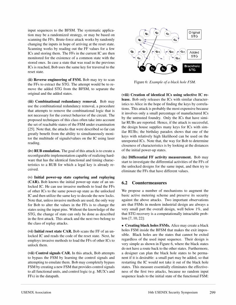
q1 q4q2 q3q0q5 q6 q7 q31q29 q30q15….…. …. ….…. …. Original STGAdded STGBlackhole STGh1 h4h2 h3Figure 6: Example of a black hole FSM.
(viii) Creation of identical ICs using selective IC re-lease. Bob only releases the ICs with similar character-istics to Alice in the hope of finding the keys by correla-tions. This attack is probably the most expensive becauseit involves only a small percentage of manufactured ICsby the untrusted foundry. Only the ICs that have simi-lar RUBs are reported. Hence, if the attack is successful,the design house supplies many keys for ICs with sim-ilar RUBs; the birthday paradox shows that one of thekeys with relatively high likelihood can be used on theunreported ICs. Note that, the way for Bob to determinecloseness of characteristics is by looking at the distancesof the initial power-up states.
(ix) Differential FF activity measurement. Bob maystart to investigate the differential activities of the FFs ofthe unlocked designs for the same input, and then try toeliminate the FFs that have different values.
6.2 Countermeasures
We propose a number of mechanisms to augment thebasic active metering scheme and preserve its securityagainst the above attacks. Two important observationsare that FSMs in modern industrial design are always avery small part the overall design, well below 1%, andthat STG recovery is a computationally intractable prob-lem [7, 10, 22]:
• Creating black holes FSMs. Alice may create a blackholes FSM inside the BFSM that makes the exit impos-sible. Black holes are the states that cannot be exitedregardless of the used input sequence. Their design isvery simple as shown in Figure 6, where the black statesdo not have a route back to the other states. Furthermore,a designer can plan the black hole states to be perma-nent if it is desirable: a small part may be added, so thatrestarting the IC would not take it out of the black holestates. This measure essentially eliminates the effective-ness of the first two attacks, because no random inputsequence leads to the initial state of the functional FSM:
16th USENIX Security SymposiumUSENIX Association 299
once the black hole sub-FSM is entered, there is no wayout. A special case is creation of trapdoor black (gray)holes FSMs that are designed in such a way that onlylong specific sequence of input signals known just to thedesigner can bring control out of this FSM and into theinitial functional state of the overall FSM. An issue thatneeds to be carefully addressed here is preventing the ICfrom powering-up in one of the black-hole states. Thiscan be easily ensured by adding extra logic to the blackhole parts that would disconnect the black hole statesfrom the power-up states.
• Merging the functional BFSM with the test andother FSMs, (e.g. ones that can be used for debuggingand authentication). In a typical design, the functionalcontrol circuits are not the only FSMs around. Alice,with the the objective to make identification of her func-tional FSM more difficult, can further intricate the BFSMby co-synthesizing them with others. This augmenta-tion makes the first two and the three CAR attacks lesseffective. In particular, this merger would distract theability to simultaneously monitor the multitude of sig-nals/values on the IC using laser reading.
• Similar FF activity for the unlocked ICs. The de-signs would be made such that once an IC exits thelocked states and is in its functional states, all its FFshave a deterministic behavior that is the same for all ICs.Thus, the differential FF activity screening would notyield any useful information.
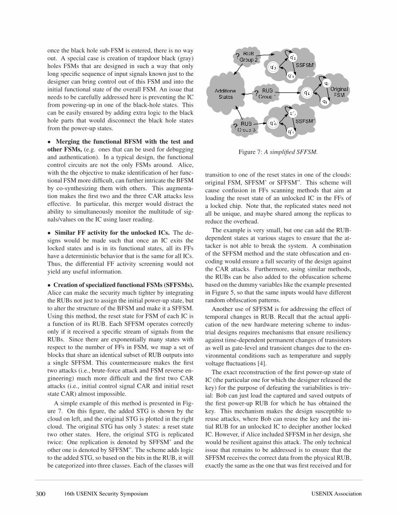
• Creation of specialized functional FSMs (SFFSMs).Alice can make the security much tighter by integratingthe RUBs not just to assign the initial power-up state, butto alter the structure of the BFSM and make it a SFFSM.Using this method, the reset state for FSM of each IC isa function of its RUB. Each SFFSM operates correctlyonly if it received a specific stream of signals from theRUBs. Since there are exponentially many states withrespect to the number of FFs in FSM, we map a set ofblocks that share an identical subset of RUB outputs intoa single SFFSM. This countermeasure makes the firsttwo attacks (i.e., brute-force attack and FSM reverse en-gineering) much more difficult and the first two CARattacks (i.e., initial control signal CAR and initial resetstate CAR) almost impossible.
A simple example of this method is presented in Fig-ure 7. On this figure, the added STG is shown by thecloud on left, and the original STG is plotted in the rightcloud. The original STG has only 3 states: a reset statetwo other states. Here, the original STG is replicatedtwice: One replication is denoted by SFFSM’ and theother one is denoted by SFFSM”. The scheme adds logicto the added STG, so based on the bits in the RUB, it willbe categorized into three classes. Each of the classes will
Additional States Original FSMq2q1q’0q”2q”1q"0 SSFSM”q’2q’1q’0 SSFSM’RUB Group 1?RUB Group 2?
RUB Group 3?Figure 7: A simplified SFFSM.
transition to one of the reset states in one of the clouds:original FSM, SFFSM’ or SFFSM”. This scheme willcause confusion in FFs scanning methods that aim atloading the reset state of an unlocked IC in the FFs ofa locked chip. Note that, the replicated states need notall be unique, and maybe shared among the replicas toreduce the overhead.
The example is very small, but one can add the RUB-dependent states at various stages to ensure that the at-tacker is not able to break the system. A combinationof the SFFSM method and the state obfuscation and en-coding would ensure a full security of the design againstthe CAR attacks. Furthermore, using similar methods,the RUBs can be also added to the obfuscation schemebased on the dummy variables like the example presentedin Figure 5, so that the same inputs would have differentrandom obfuscation patterns.
Another use of SFFSM is for addressing the effect oftemporal changes in RUB. Recall that the actual appli-cation of the new hardware metering scheme to indus-trial designs requires mechanisms that ensure resiliencyagainst time-dependent permanent changes of transistorsas well as gate-level and transient changes due to the en-vironmental conditions such as temperature and supplyvoltage fluctuations [4].
The exact reconstruction of the first power-up state ofIC (the particular one for which the designer released thekey) for the purpose of defeating the variabilities is triv-ial: Bob can just load the captured and saved outputs ofthe first power-up RUB for which he has obtained thekey. This mechanism makes the design susceptible toreuse attacks, where Bob can reuse the key and the ini-tial RUB for an unlocked IC to decipher another lockedIC. However, if Alice included SFFSM in her design, shewould be resilient against this attack. The only technicalissue that remains to be addressed is to ensure that theSFFSM receives the correct data from the physical RUB,exactly the same as the one that was first received and for
16th USENIX Security Symposium USENIX Association300
which the key is available. Otherwise, the stored key willfail.
In presence of temporal variations, ensuring that eachSFFSM receives the correct data from RUB requireserror-correction mechanisms. One solution is to em-ploy standard error-correction codes (ECCs). An alterna-tive hardware solution that encounters a lower overheadcompared to ECC is to create the specifications of eachSFFSM in such a way that it transitions into the correctnext states, even when one or up to a specified number ofthe inputs from the RUB are altered by the environmentalconditions. Using the hamming distances of the RUBs,we can group them into similar SFFSMs and synthesizethe results such that the error correction mechanisms areinherently present. This mechanism is particularly effec-tive for longer RUBs that are required for present indus-trial designs. Note that, because the minterms for thecombinational logic that implements transitions are nownot smaller than for non-resilient versions of the SFFSM,the hardware overhead is often zero or negative at theexpense of the lower resiliency against brute force at-tacks [5]. However, since the probability of brute forceattack can be made arbitrarily small with very low over-head (i.e., by using the black holes), this is a favorabletrade-off.
• Resiliency against combinational redundancy re-moval. To overcome this attack, Alice must ensure theinapplicability of the attack to typical large circuits andthe capability of this method to remove the added states.In general, computing a set of reachable states, can onlybe done for relatively small circuits, even when the im-plicit enumeration techniques are used. Thus, the methodis only applicable to small circuits of small sizes.
• Statistical characterization of gates. Alice can goone step further and attempt to derive the gate-level char-acteristics of the manufactured ICs by measuring the in-put/output signals and exploiting the controllability andobservability into the design. Essentially, knowing thecircuit diagram, she would be able to write a linear sys-tems of equations that can be solved for obtaining theapproximate gate-level delay and power characteristicsof the gates. She may even go further to use the extracteddata to find the distribution of variations across the dif-ferent chips (e.g., by using methods such as expectationmaximization(EM)). Now, if the variations do not haveenough fluctuations, then she will get suspicious and canhalt the unlocking. This computation would ensure thatthe selective IC release would not be successful.
• Obfuscation of state activities and encodings. Theimplementation of the BFSM presented in the previoussection renders it impossible to tell the difference be-tween the original FSM FFs and the added states FFs.
This is because all of the FFs are changing all the time.Therefore, even though two states of BFSM in two ICsmight be identical, the attacks based on scanning theFFs would not notice that, since a subset of the bitswill be different. In other word, the FFs not used inthe added FSM are randomly changing. Another ob-fuscation method that has already been implemented isthat the states in the added STG are not in order and arecoded out of sequence by the synthesis tool. Thus, eventhough there might be a direct transition (edge) betweentwo states, the methods based on FFs readings would notnotice the proximity of the two states, since there codewords are distant from each other.
Note that, the attacks that were described earlier, eventhe ones that are computationally very expensive, willnot be able to unlock the ICs, if the countermeasures de-scribed above are in place.
7 Experimental evaluations
To test the applicability of the method described earlier,we implemented the active hardware metering on stan-dard benchmark designs. In this section, we present theexperimental setup, followed by the overhead of imple-menting BFSM on the considered benchmarks. Afterthat, we show quantitative analysis of the effectivenessof the brute force attacks. We further show how the addi-tion of black holes can make the scheme resilient againstthis attack with a minimal overhead. Note that, manyof the attacks described earlier are assuming structuralcountermeasures that are hard to quantify and evaluate.
7.1 Experiment setupWe used extended set of sequential benchmarks from theISCAS’89 to evaluate the impact of the active hardwaremetering method [6]. Even though the ISCAS’89 bench-marks are the latest comprehensive set of the gate-leveldesigns, they are dated compared to the complex circuitsin design, production and use today. Recall that follow-ing the Moore’s law, the size and complexity of the cir-cuits doubles approximately every 18 months. We usethe larger benchmarks from the set, and we project theresults to more complex circuits. Our projections showthat the power, area, and delay overheads diminish as weincrease the size and complexity. Simultaneously, thelocking complexity and resiliency against the attacks ex-ponentially improves, due the multiplicity of states. Wesynthesize the benchmarks using the Berkeley SIS tool[26], that given a STG or a logic-level description of a se-quential circuit produces an optimized netlist in the targettechnology (cell library) while preserving the sequentialinput-output behavior. We have written a C program thatmodifies the benchmarks by adding the extra states. The
16th USENIX Security SymposiumUSENIX Association 301
program calls SIS to obtain the specifications of the syn-thesized and mapped original and modified STGs. Whenevaluating the overhead results, the important observa-tion is that FSMs (i.e., the control circuitry) in modernindustrial design are always a very small part of the over-all design, well bellow 1% [7, 10]. Thus, even doublingthe overhead, will have a minimal impact on the overallcircuit that is mostly occupied by memory, testing pins,and data path circuitry.
7.2 Overhead of active hardware metering
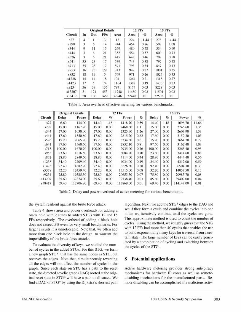
Our first set of experiments study the overhead of the in-troduced scheme in terms of area, power, and delay. Itis worth noting here that our ultimate goal is to integratethe active hardware metering method in the design flow.Thus we have considered testing the approach on manu-factured ICs. However, the prohibitive cost of manufac-turing a circuit in aggressive technologies (the quote wegot for fabricating a circuit in 65nm was $500K) limitsour experiments to synthesizing the benchmarks. Table 1presents the results for the area overhead. Because ofthe relatively small size of the circuits, we added STGswith 12 FFs and 15 FFs overhead to the original STGs.The first column shows the name of the circuit from theISCAS’89 benchmark. The second column shows thenumber of inputs to the circuit. The third column showsthe number of outputs to the circuits. Both the numberof inputs and the number of outputs do not change af-ter adding the extra states. The fourth column shows thenumber of FFs in the original circuit. The fifth columnshows the area of the original circuit. Then we show boththe new area and the percentage overhead after adding 12FFs and 15 FFs for the extra states. It can be seen that thepercentage area overhead is decreasing as the circuit sizeincreases. Thus, for larger circuit sizes, the area overheadwill be even less insignificant.
Table 2 shows the delay and power overheads. Thefirst column contains the benchmark names. The secondand third columns show the delay and power estimates ofthe original circuits. These are followed by both the de-lay and the percentage delay overhead, and the power andthe percentage power overhead for adding both 12 FFsand 15 FFs STGs respectively. The delay overheads areuniversally small. With the exception of s27 that is toosmall to be considered practical, it is interesting to seethat even other small benchmarks encountered no delayoverhead after the addition of the new STG. For the smallbenchmarks that are not realistic compared to the currentcomplex designs, the power increases significantly. Asthe circuit size increases, the percentage power overheaddecreases.
Next, we make a small model of the percentage of areaand power overhead versus size of the circuit to extrapo-
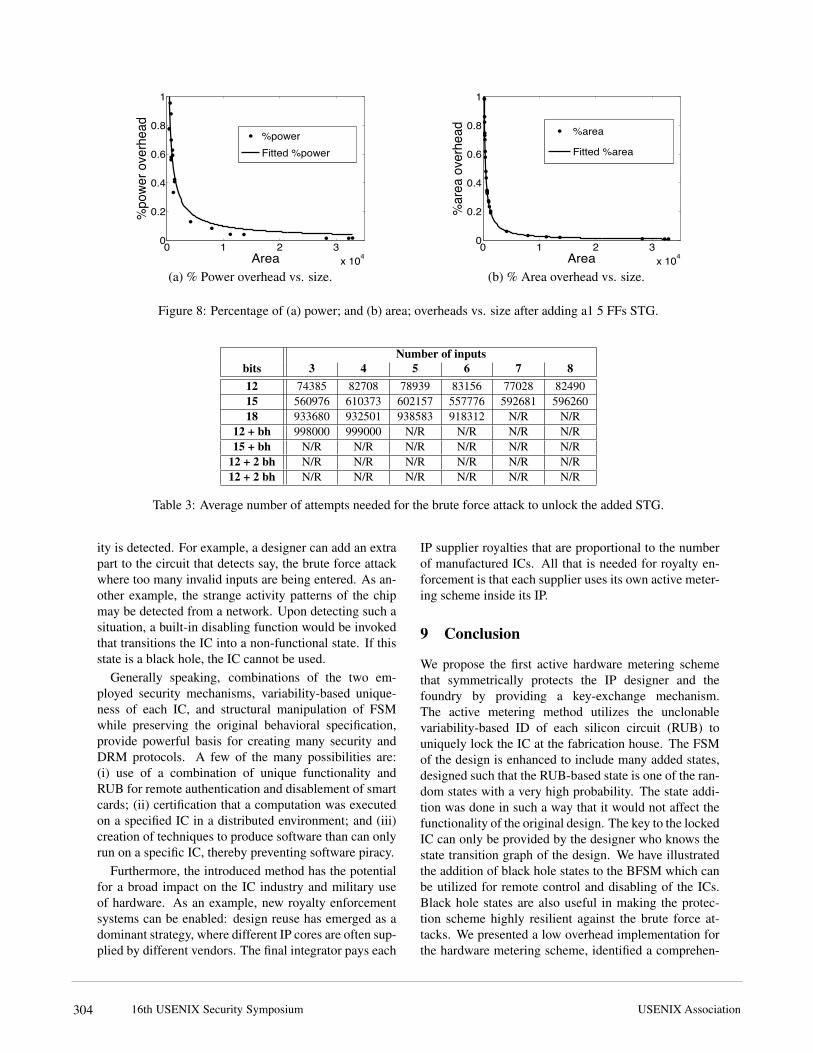
late to more complex designs. The size of the added STGis fixed to 15 FFs. Figures 8(a) and 8(b) show the over-head data vs. size along with the fitted polynomial mod-els, for power and area respectively. The plots suggestthat as the circuit size increases, the percentage of powerand area overheads both decrease. Note that, for morecomplex designs, it is required to add significantly morethan 15 FFs. Even if adding a STG with 100 FFs wouldadd six times the overhead of the 15 FFs case in absoluteterms, the overhead would be negligible, while there willbe 285 extra states added to the design. Thus, for currentand future circuit technologies, the BFSM would have aminimal impact on the performance in terms of power,area, and delay (i.e., it will most likely stay less than 1%of the overall design).
7.3 Resiliency against the brute force at-tack
Most of the attacks described in Section 6 can be en-countered by devising intelligent design strategies, as de-scribed in Subsection 6.2. The only attack that we quan-titatively study here is the brute force attack. We modelthis attack by randomly guessing the values on the graphuntil arriving at the functional reset state of the originalFSM.
We simulated the brute force attack on BFSMs with12, 15, and 18 FFs, varying the inputs from 3 to 8. In thisexperiment, we set an upper bound of 1,000,000 guesses;if the reset state is not reached after this many trials,the original STG is considered unreachable (denoted byN/R) and the brute force attack is reported unsuccessful.
Table 3 shows the average number of guesses neededto unlock the BFSM over a 10,000 simulation runs. Thefirst three rows show added STGs with 12, 15, and 18FFs respectively. The next two rows show the results forSTGs with 12 and 15 FFs, after adding 1 and 2 blackholes respectively. Although the number of inputs doesnot affect the overhead, it impacts the resiliency againstthe brute force attack: the table illustrates that the bruteforce attacks are less successful if we use more than 3different inputs. Also, as the size of the added STG in-creases, more guesses are necessary to unlock the circuit.By adding one black hole to the smaller FSMs, they per-form better than the larger FSMs. Adding one or twoblack holes makes the original STG unreachable for thebrute force attack. It is worth noting here that STGs with12 and 15 FFs are really small, as they have a total of4,096 and 32,768 states respectively. If the active meter-ing scheme was to be implemented on current industrialstrength designs, the added circuit would have at least a100 FFs that would create 2100 ∼ 1030 states. It wouldbe impossible for a brute force attack to find a key. Fur-thermore, addition of a few black holes will further make
16th USENIX Security Symposium USENIX Association302
Original Details 12 FFs 15 FFsCircuit In Out FFs Area Area % Area %
s27 4 1 3 18 224 11.44 278 14.44s298 3 6 14 244 454 0.86 508 1.08s344 9 11 15 269 480 0.78 534 0.99s444 3 6 21 352 554 0.57 609 0.73s526 3 6 21 445 648 0.46 702 0.58s641 35 23 17 539 743 0.38 797 0.48s713 35 23 17 591 793 0.34 847 0.43s953 16 23 29 743 947 0.27 1001 0.35s832 18 19 5 769 971 0.26 1025 0.33
s1238 14 14 18 1041 1264 0.21 1318 0.27s1423 17 5 74 1164 1382 0.19 1436 0.23s9234 36 39 135 7971 8174 0.03 8228 0.03s13207 31 121 453 11248 11450 0.02 11504 0.02s38417 28 106 1463 32246 32448 0.01 32502 0.01
Table 1: Area overhead of active metering for various benchmarks.
Original Details 12 FFs 15 FFsCircuit Delay Power Delay % Power % Delay % Power %
s27 6.60 134.00 14.40 1.18 1418.70 9.59 14.40 1.18 1696.70 11.66s298 15.00 1167.20 15.00 0.00 2468.60 1.11 15.00 0.00 2746.60 1.35s344 27.00 1030.00 27.00 0.00 2325.90 1.26 27.00 0.00 2603.90 1.53s444 17.60 1550.80 17.60 0.00 2815.20 0.82 17.60 0.00 3152.30 1.03s526 15.20 2065.70 15.20 0.00 3334.30 0.61 15.20 0.00 3664.70 0.77s641 97.60 1560.60 97.60 0.00 2832.10 0.81 97.60 0.00 3162.40 1.03s713 100.00 1670.70 100.00 0.00 2935.00 0.76 100.00 0.00 3265.40 0.95s953 23.60 1816.50 23.60 0.00 3084.20 0.70 23.60 0.00 3414.60 0.88s832 28.80 2849.60 28.80 0.00 4114.00 0.44 28.80 0.00 4444.40 0.56
s1238 34.40 2709.40 34.40 0.00 4034.00 0.49 34.40 0.00 4312.00 0.59s1423 92.40 4882.70 92.40 0.00 6226.30 0.28 92.40 0.00 6504.30 0.33s5378 32.20 12459.40 32.20 0.00 13515.00 0.08 32.20 0.00 14057.50 0.13s9234 75.80 19385.50 75.80 0.00 20653.30 0.07 75.80 0.00 20983.70 0.08
s13207 85.60 37874.00 85.60 0.00 39138.40 0.03 85.60 0.00 39402.00 0.04s38417 69.40 112706.80 69.40 0.00 113869.00 0.01 69.40 0.00 114147.00 0.01
Table 2: Delay and power overhead of active metering for various benchmarks.
the system resilient against the brute force attack.
Table 4 shows area and power overheads for adding ablack hole with 2 states to added STGs with 12 and 15FFs respectively. The overhead of adding a black holedoes not exceed 5% even for very small benchmarks. Forlarger circuits it is unnoticeable. Note that, we often addmore than one black hole to the design, to warrant theimpossibility of the brute force attacks.
To evaluate the diversity of keys, we studied the num-ber of cycles in the added STGs. For this STG, we forma new graph STG*, that has the same nodes as STG, butreverses the edges. Note that, simultaneously reversingall the edges will not affect the number of cycles in thegraph. Since each state on STG has a path to the resetstate, the directed acyclic graph (DAG) rooted at the orig-inal reset state in STG* will have a path to all states. Wefind a DAG of STG* by using the Dijkstra’s shortest path
algorithm. Next, we add the STG* edges to the DAG andsee if they form a cycle and combine the cycles into onenode; we iteratively continue until the cycles are gone.This approximate method is used to count the number ofcycles. Using the method, we roughly guess that the STGwith 12 FFs had more than 40 cycles that enables the useto build exponentially many keys for traversal from a cer-tain state. The large number of keys can be easily gener-ated by a combination of cycling and switching betweenthe cycles of the STG.
8 Potential applications
Active hardware metering provides strong anti-piracymechanisms for hardware IP cores as well as remote-disabling mechanisms for the manufactured parts. Re-mote disabling can be accomplished if a malicious activ-
16th USENIX Security SymposiumUSENIX Association 303
0 1 2 3x 10⁴
0
0.2
0.4
0.6
0.8
1
Area
%po
wer o
verh
ead
%powerFitted %power
(a) % Power overhead vs. size.
0 1 2 3x 10⁴
0
0.2
0.4
0.6
0.8
1
Area
%ar
ea o
verh
ead %area
Fitted %area
(b) % Area overhead vs. size.
Figure 8: Percentage of (a) power; and (b) area; overheads vs. size after adding a1 5 FFs STG.
Number of inputsbits 3 4 5 6 7 812 74385 82708 78939 83156 77028 8249015 560976 610373 602157 557776 592681 59626018 933680 932501 938583 918312 N/R N/R
12 + bh 998000 999000 N/R N/R N/R N/R15 + bh N/R N/R N/R N/R N/R N/R
12 + 2 bh N/R N/R N/R N/R N/R N/R12 + 2 bh N/R N/R N/R N/R N/R N/R
Table 3: Average number of attempts needed for the brute force attack to unlock the added STG.
ity is detected. For example, a designer can add an extrapart to the circuit that detects say, the brute force attackwhere too many invalid inputs are being entered. As an-other example, the strange activity patterns of the chipmay be detected from a network. Upon detecting such asituation, a built-in disabling function would be invokedthat transitions the IC into a non-functional state. If thisstate is a black hole, the IC cannot be used.
Generally speaking, combinations of the two em-ployed security mechanisms, variability-based unique-ness of each IC, and structural manipulation of FSMwhile preserving the original behavioral specification,provide powerful basis for creating many security andDRM protocols. A few of the many possibilities are:(i) use of a combination of unique functionality andRUB for remote authentication and disablement of smartcards; (ii) certification that a computation was executedon a specified IC in a distributed environment; and (iii)creation of techniques to produce software than can onlyrun on a specific IC, thereby preventing software piracy.
Furthermore, the introduced method has the potentialfor a broad impact on the IC industry and military useof hardware. As an example, new royalty enforcementsystems can be enabled: design reuse has emerged as adominant strategy, where different IP cores are often sup-plied by different vendors. The final integrator pays each
IP supplier royalties that are proportional to the numberof manufactured ICs. All that is needed for royalty en-forcement is that each supplier uses its own active meter-ing scheme inside its IP.
9 Conclusion
We propose the first active hardware metering schemethat symmetrically protects the IP designer and thefoundry by providing a key-exchange mechanism.The active metering method utilizes the unclonablevariability-based ID of each silicon circuit (RUB) touniquely lock the IC at the fabrication house. The FSMof the design is enhanced to include many added states,designed such that the RUB-based state is one of the ran-dom states with a very high probability. The state addi-tion was done in such a way that it would not affect thefunctionality of the original design. The key to the lockedIC can only be provided by the designer who knows thestate transition graph of the design. We have illustratedthe addition of black hole states to the BFSM which canbe utilized for remote control and disabling of the ICs.Black hole states are also useful in making the protec-tion scheme highly resilient against the brute force at-tacks. We presented a low overhead implementation forthe hardware metering scheme, identified a comprehen-
16th USENIX Security Symposium USENIX Association304
12 FFs 15 FFsCircuit % Area % Power % Area % Power
s27 0.05 0.04 0.04 0.03s298 0.02 0.02 0.02 0.02s344 0.04 0.02 0.03 0.02s444 0.03 0.02 0.02 0.02s526 0.01 0.02 0.01 0.02s641 0.02 0.02 0.02 0.02s713 0.01 0.02 0.01 0.02s953 0.02 0.02 0.02 0.02s832 0.02 0.01 0.02 0.01s1238 0.01 0.01 0.01 0.01s1423 0.01 0.01 0.01 0.01s5378 0.00 0.00 0.00 0.00s9234 0.00 0.00 0.00 0.00
s13207 0.00 0.00 0.00 0.00s38417 0.00 0.00 0.00 0.00
Table 4: Percentage of area and power overheads afteradding one blackhole.
sive set of possible attacks, and provided mechanismsthat make the scheme much more resilient against the at-tacks. Experimental evaluations of the proposed meter-ing method on standard benchmark circuits illustrate thelow overhead and the applicability of the approach onindustrial-size designs and its resiliency against differentattacks.
10 Acknowledgement
This work is supported by the Defense Advanced Re-search Projects Agency (DARPA)/MTO Trust in Inte-grated Circuits and Young Faculty Awards (YFA) undergrant award W911NF-07-1-0198.
References
[1] D.G. Abraham, G.M. Dolan, G.P. Double, and J.V.Stevens. Transaction security system. IBM SystemsJournal, 30(2):206–229, 1991.
[2] R. Anderson and M. Kuhn. Tamper resistance -a cautionary note. In USENIX Workshop on Elec-tronic Commerce, pages 1–11, 1996.
[3] R.J. Anderson. Security Engineering: A guide tobuilding dependable distributed systems. John Wi-ley and Sons, 2001.
[4] K. Bernstein, D.J. Frank, A.E. Gattiker, W. Haen-sch, B.L. Ji, S.R. Nassif, E.J. Nowak, D.J. Pearson,and N.J. Rohrer. High-performance CMOS vari-ability in the 65-nm regime and beyond. IBM Jour-nal of Research and Development, 50(4/5):433–450, 2006.
[5] R.K. Brayton, G. Hachtel, C. McMullen, andA. Sangiovanni-Vincentelli. Logic MinimizationAlgorithms for VLSI Synthesis. Kluwer AcademicPublishers, 1984.
[6] F. Brgles, D. Bryan, and K. Kozminski. Combina-tional profiles of sequential benchmark circuits. InInternational Symposium of Circuits and Systems,pages 1929–1934, 1989.
[7] A.P. Chandrakasan, M. Potkonjak, R. Mehra,J. Rabaey, and R.W. Brodersen. Optimizing powerusing transformations. IEEE Trans. CAD of Inte-grated Circuits and Systems, 14(1):12–31, 1995.
[8] Defense Science Board (DSB) study onHigh Performance Microchip Supply.http://www.acq.osd.mil/dsb/reports/2005-02-HPMS Report Final.pdf, 2005.
[9] B. Gassend, D. Lim, D. Clarke, M. van Dijk, andS. Devadas. Concurrency and Computation: Prac-tice and Experience, volume 16, chapter Identifica-tion and authentication of integrated circuits, pages1077–1098. John Wiley & Sons, 2004.
[10] J.L. Hennessy and D.A. Patterson. Computer ar-chitecture: a quantitative approach. Morgan Kauf-mann Publishers, 1996.
[11] A. Kahng, J. Lach, W. Mangione-Smith, S. Man-tik, I. Markov, M. Potkonjak, P. Tucker, H. Wang,and G. Wolfe. Watermarking techniques for intel-lectual property protection. In Design AutomationConference (DAC), pages 776–781, 1998.
[12] D. Kirovski, Y.-Y. Hwang, M. Potkonjak, andJ. Cong. Intellectual property protection by water-marking combinational logic synthesis solutions. InInternational Conference on Computer Aided De-sign (ICCAD), pages 194–198, 1998.
[13] D. Kirovski and M. Potkonjak. Local watermarks:methodology and application to behavioral synthe-sis. IEEE Trans. CAD, 22(9):1277–1283, 2003.
[14] F. Koeune and F. Standaert. A tutorial on physicalsecurity and side-channel attacks. In Foundationsof Security Analysis and Design (FOSAD), pages78–108, 2004.
[15] F. Koushanfar, I. Hong, and M. Potkonjak. Be-havioral synthesis techniques for intellectual prop-erty protection. ACM Trans. Design Automation ofElectronic Systems, 10(3):523–545, 2005.
[16] F. Koushanfar and G. Qu. Hardware metering. InDesign Automation Conference (DAC), pages 490–493, 2001.
16th USENIX Security SymposiumUSENIX Association 305
[17] F. Koushanfar, G. Qu, and M. Potkonjak. Intel-lectual property metering. In Information HidingWorkshop (IHW), pages 81–95, 2001.
[18] J. Lach, W.H. Mangione-Smith, and M. Potkonjak.Fingerprinting digital circuits on programmablehardware. In Information Hiding Workshop (IHW),pages 16–32, 1998.
[19] J.W. Lee, L. Daihyun, B. Gassend, G.E. Suh,M. van Dijk, and S. Devadas. A technique to builda secret key in integrated circuits for identificationand authentication applications. In Symposium ofVLSI Circuits, pages 176–179, 2004.
[20] K. Lofstrom, W.R. Daasch, and D. Taylor. IC iden-tification circuits using device mismatch. In Inter-national Solid State Circuits Conference (ISSCC),pages 372–373, 2000.
[21] S. Maeda, H. Kuriyama, T. Ipposhi, S. Maegawa,Y. Inoue, M. Inuishi, N. Kotani, and T. Nishimura.An artificial fingerprint device (AFD): a study ofidentification number applications utilizing charac-teristics variation of polycrystalline silicon TFTs.IEEE Trans. Electron Devices, 50(6):1451–1458,2003.
[22] A. Oliveira. Techniques for the creation of digi-tal watermarks in sequential circuit designs. IEEETrans. CAD of Integrated Circuits and Systems,20(9):1101–1117, 2001.
[23] G. Qu and M. Potkonjak. Intellectual Property Pro-tection in VLSI Design. Kluwer Academic Pub-lisher, 2003.
[24] S. Roy and A. Asenov. Where do the dopants go?Science, 309(5733):388–390, 2005.
[25] H. Savoj and R.K. Brayton. On the optimizationpower of retiming and resynthesis transformations.In Design Automation Conference (DAC), pages297–301, 1990.
[26] E.M. Sentovich, K.J. Singh, L. Lavagno, C. Moon,R. Murgai, A. Saldanha, H. Savoj, P.R. Stephan,R.K. Brayton, and A.L. Sangiovanni-Vincentelli.SIS: A system for sequential circuit synthesis.Technical Report UCB/ERL M92/41, EECS De-partment, University of California, Berkeley, 1992.
[27] A. Srivastava, D. Sylvester, and D. Blaauw. Statis-tical Analysis and Optimization for VLSI: Timingand Power. Series on Integrated Circuits and Sys-tems. Springer, 2005.
[28] Y. Su, J. Holleman, and B. Otis. A 1.6J/bit sta-ble chip ID generating circuit using process varia-tions. In International Solid State Circuits Confer-ence (ISSCC), page to appear, 2007.
[29] G.E. Suh, C.W. O’Donnell, I. Sachdev, and S. De-vadas. Design and implementation of the aegissingle-chip secure processor using physical randomfunctions. In International Symposium on Com-puter Architecture (ISCA), pages 25–36, 2005.
[30] I. Torunoglu and E. Charbon. Watermarking-basedcopyright protection of sequential functions. IEEEJournal of Solid-State Circuits (JSSC), 35(3):434–440, 2000.
[31] VSI Alliance - Intellectual Property Protec-tion Development Working Group, “White Paper:The Value and Management of Intellectual Assets”.http://vsi.org/documents/datasheets/TOC IPPWP210.pdf,2002.
[32] J.L. Wong, R. Majumdar, and M. Potkonjak. Fairwatermarking using combinatorial isolation lem-mas. IEEE Trans. CAD, 23(11):1566–1574, 2004.
Notes1In this paper, the term IP is used to refer to the integrated circuits
design specifications that is available to the fabrication house.
16th USENIX Security Symposium USENIX Association306