Embed Size (px)
Citation preview

D. Pribat
IWORID ’05. 4-7 July 2005. ESRF Grenoble
Active matrix back planes for the control of large area X-ray imagers
D. Pribat and C. CojocaruLaboratoire de Physique des Interfaces et des Couches
MincesEcole Polytechnique
91128, Palaiseau, France
D. Pribat
IWORID ’05. 4-7 July 2005. ESRF Grenoble
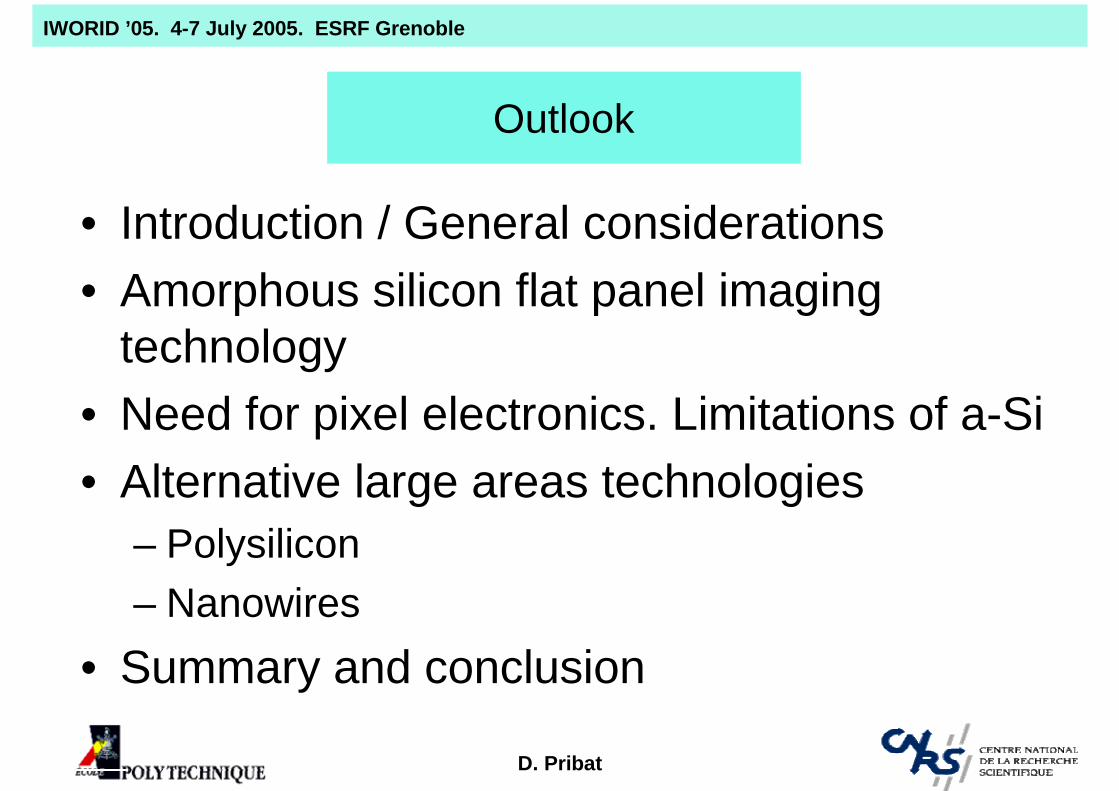
Outlook
• Introduction / General considerations• Amorphous silicon flat panel imaging
technology• Need for pixel electronics. Limitations of a-Si• Alternative large areas technologies
– Polysilicon– Nanowires
• Summary and conclusion

D. Pribat
IWORID ’05. 4-7 July 2005. ESRF Grenoble
Solid state X-ray imagers
• c-Si based detectors– Linear arrays
• Diodes• Microstrips
– Two dimensional detectors• CCD: max surface ~ 8x10 cm2 (eg., CCD595, Fairchild Imaging)• CMOS: max surface ~ 17x22 cm2 (C7830-01, Hamamatsu)
• a-Si:H based detectors
Wafer Scale Integration ⇒ Yield?
D. Pribat
IWORID ’05. 4-7 July 2005. ESRF Grenoble
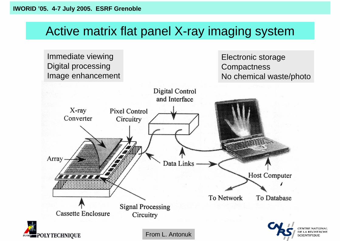
Active matrix flat panel X-ray imaging system
Electronic storageCompactnessNo chemical waste/photo
Immediate viewingDigital processingImage enhancement
From L. Antonuk
D. Pribat
IWORID ’05. 4-7 July 2005. ESRF Grenoble
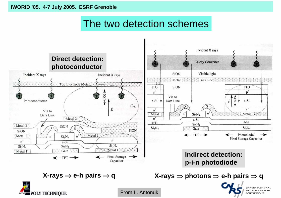
Indirect detection:p-i-n photodiode
Direct detection:photoconductor
The two detection schemes
X-rays ⇒ e-h pairs ⇒ q
From L. Antonuk
X-rays ⇒ photons ⇒ e-h pairs ⇒ q
D. Pribat
IWORID ’05. 4-7 July 2005. ESRF Grenoble
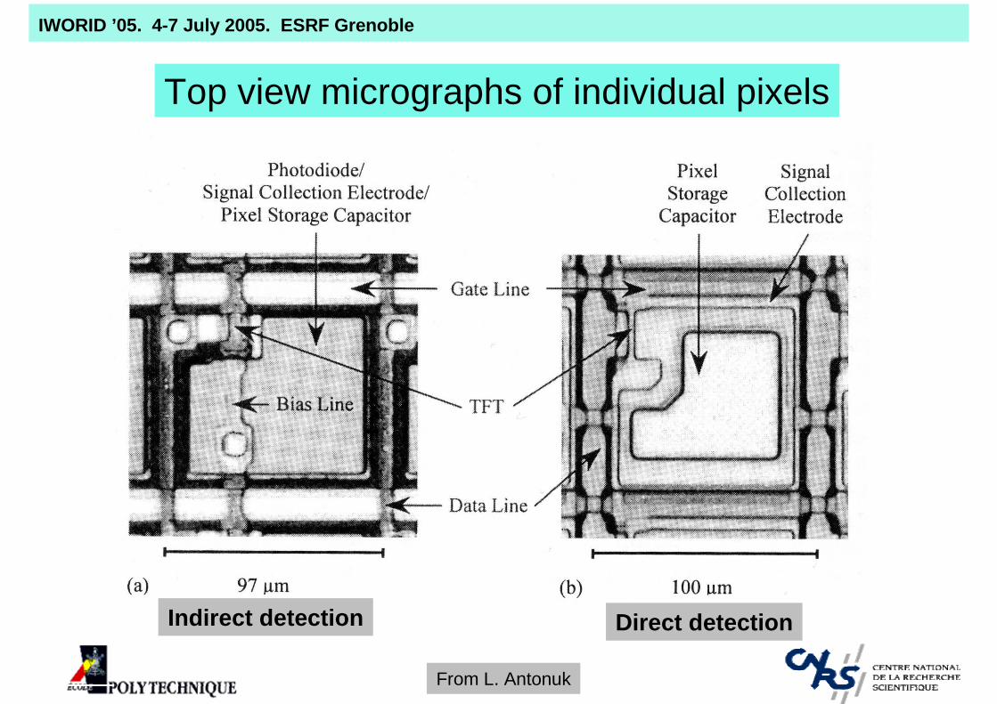
Indirect detection
From L. Antonuk
Direct detection
Top view micrographs of individual pixels

D. Pribat
IWORID ’05. 4-7 July 2005. ESRF Grenoble
Imaging array
Pixel
VB (Bias line)
CST
READ CFB
Column Charge
Amplifier
Data line
Gate line
Pixell
General organisation of an active matrix detector

D. Pribat
IWORID ’05. 4-7 July 2005. ESRF Grenoble
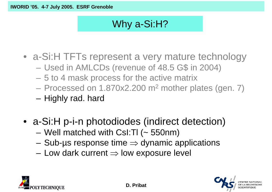
Why a-Si:H?
• a-Si:H TFTs represent a very mature technology– Used in AMLCDs (revenue of 48.5 G$ in 2004)– 5 to 4 mask process for the active matrix– Processed on 1.870x2.200 m2 mother plates (gen. 7)– Highly rad hard
• a-Si:H p-i-n photodiodes (indirect detection) – Well matched with CsI:Tl (~ 550nm)– Sub-µs response time ⇒ dynamic applications– Low dark current ⇒ low exposure level
D. Pribat
IWORID ’05. 4-7 July 2005. ESRF Grenoble
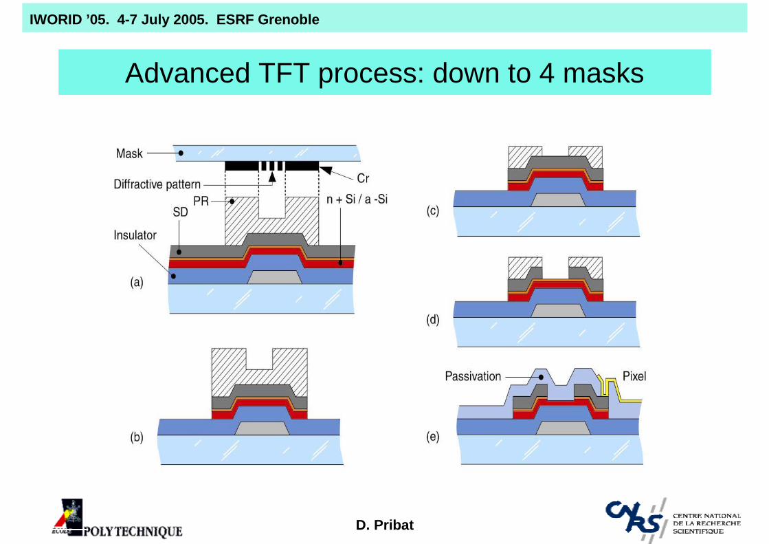
Advanced TFT process: down to 4 masks
D. Pribat
IWORID ’05. 4-7 July 2005. ESRF Grenoble
Why a-Si:H?
• a-Si:H TFTs represent a very mature technology– Used in AMLCDs (revenue of 48.5 G$ in 2004)– 5 to 4 mask process for the active matrix– Processed on 1.870x2.200 m2 mother plates (gen. 7)– Highly rad. hard
• a-Si:H p-i-n photodiodes (indirect detection) – Well matched with CsI:Tl (~ 550nm)– Sub-µs response time ⇒ dynamic applications– Low dark current ⇒ low exposure level
D. Pribat
IWORID ’05. 4-7 July 2005. ESRF Grenoble
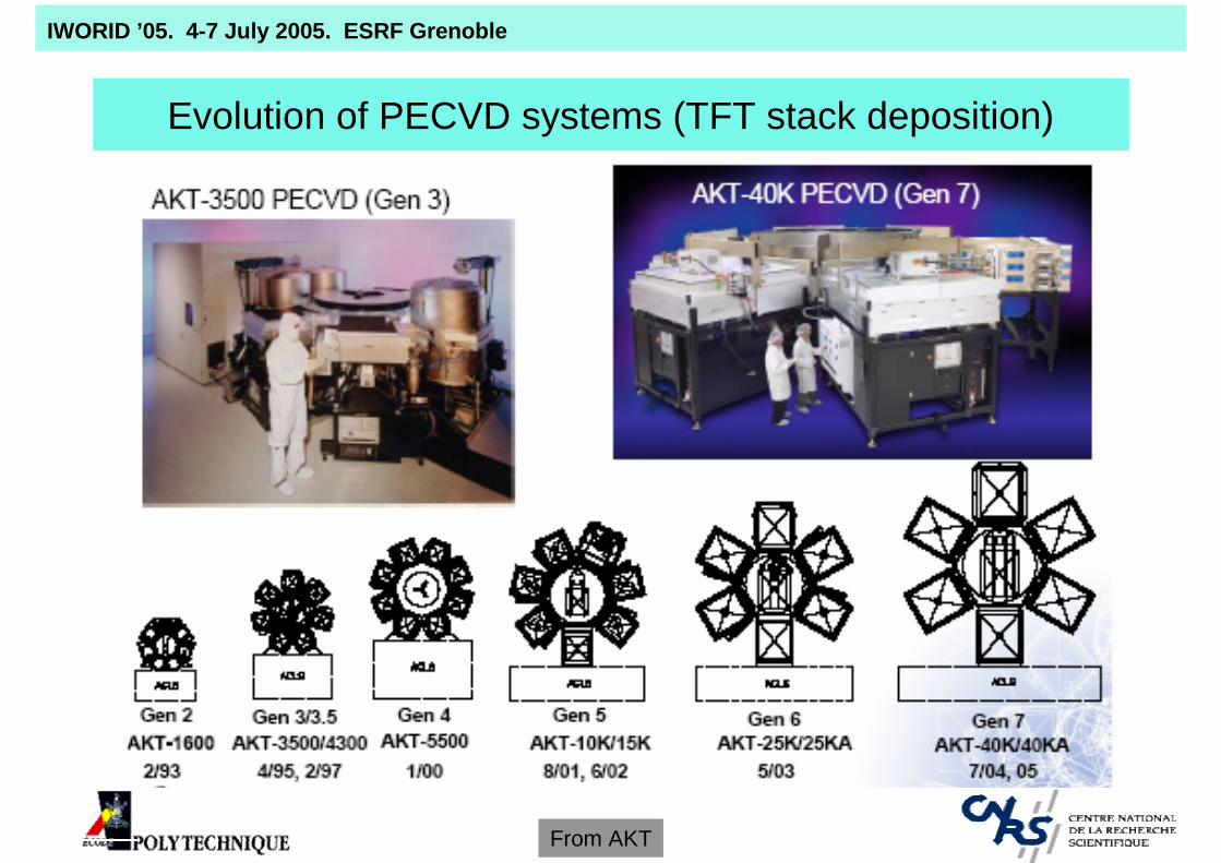
Evolution of PECVD systems (TFT stack deposition)
From AKT

D. Pribat
IWORID ’05. 4-7 July 2005. ESRF Grenoble
Recent evolution of LCD panel prices
From Display Search
D. Pribat
IWORID ’05. 4-7 July 2005. ESRF Grenoble
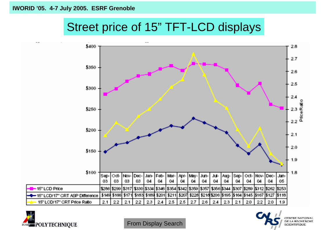
Street price of 15” TFT-LCD displays
From Display Search
D. Pribat
IWORID ’05. 4-7 July 2005. ESRF Grenoble
Why a-Si:H?
• a-Si:H TFTs represent a very mature technology– Used in AMLCDs (revenue of 48.5 G$ in 2004)– 5 to 4 mask process for the active matrix– Processed on 1.870x2.200 m2 mother plates (gen. 7)– Highly rad. hard
• a-Si:H p-i-n photodiodes (indirect detection) – Well matched with CsI:Tl (~ 550nm)– Sub-µs response time ⇒ dynamic applications– Low dark current ⇒ low exposure level

D. Pribat
IWORID ’05. 4-7 July 2005. ESRF Grenoble
0.0001 – 0.010.6 – 2400.03 – 3Exposure range (mR)
8030120X-ray spectrum (kVp)
33 ms/frame< 5 < 5Image readout time (s)
1000 x 10003600 x 48001750 x 2150Pixel count
250 x 25050 x 50150 x 150Pixel area (µm2)
25 x 2518 x 24 35 x 43Imager size (cm)
FluoroscopyMammographyRadiography
Some requirements for medical imaging
D. Pribat
IWORID ’05. 4-7 July 2005. ESRF Grenoble
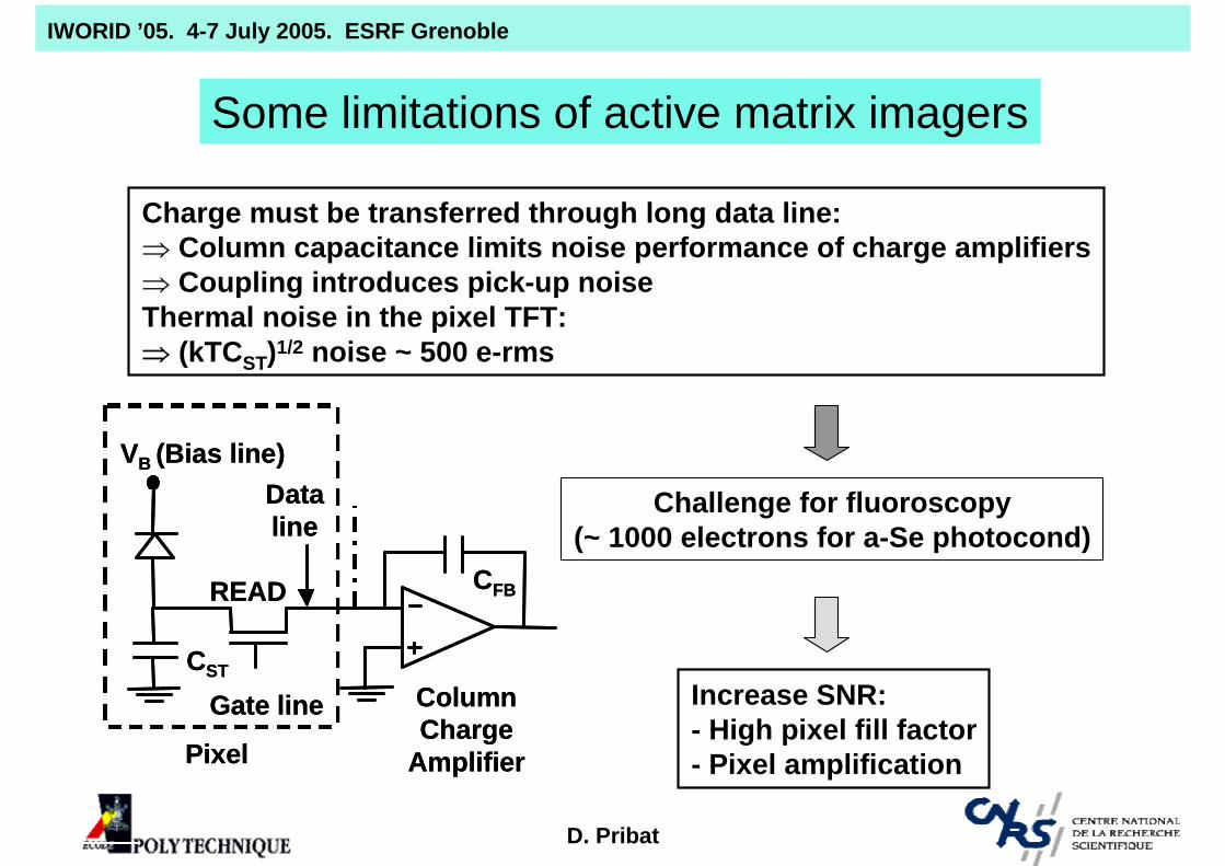
Charge must be transferred through long data line: ⇒ Column capacitance limits noise performance of charge amplifiers⇒ Coupling introduces pick-up noiseThermal noise in the pixel TFT:⇒ (kTCST)1/2 noise ~ 500 e-rms
Pixel
VB (Bias line)
CST
READ CFB
Column Charge
Amplifier
Data line
Gate line
Pixel
VB (Bias line)
CST
READ CFB
Column Charge
Amplifier
Data line
Gate line
Some limitations of active matrix imagers
Increase SNR:- High pixel fill factor- Pixel amplification
Challenge for fluoroscopy(~ 1000 electrons for a-Se photocond)
D. Pribat
IWORID ’05. 4-7 July 2005. ESRF Grenoble
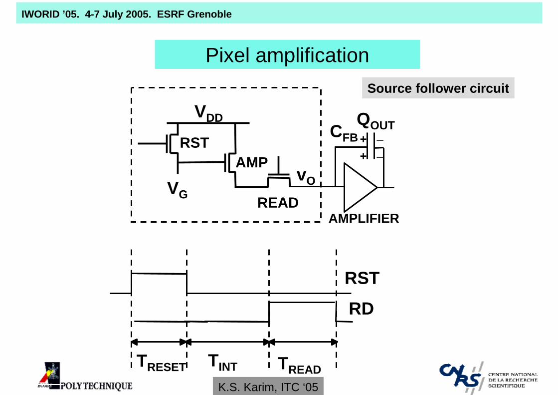
Pixel amplification
AMPLIFIER
CFB ++
__
AMP
READ
RST
VG
QOUTVDD
vO
TRESET TINT TREAD
RST
RD
K.S. Karim, ITC ‘05
Source follower circuit

D. Pribat
IWORID ’05. 4-7 July 2005. ESRF Grenoble
Charge gain for pixel amplification (a-Si:H TFTs)
0 1 2 30 1 2 3
CPIX = 1 pF
CPIX = 2 pF
CPIX = 4 pFCPIX = 10 pF
Gi = 13.3
Gi = 6.7
Gi = 3.3Gi = 1.3
QP (fC)
0
10
20
30
QO
UT
(fC)
10 pF++
__
hν+ +– –
QOUT
VDD
CPIXQP
60/25150/25
150/25
OK for fluoroscopybut signal saturationfor radiography!!
K.S. Karim, ITC ‘05
D. Pribat
IWORID ’05. 4-7 July 2005. ESRF Grenoble
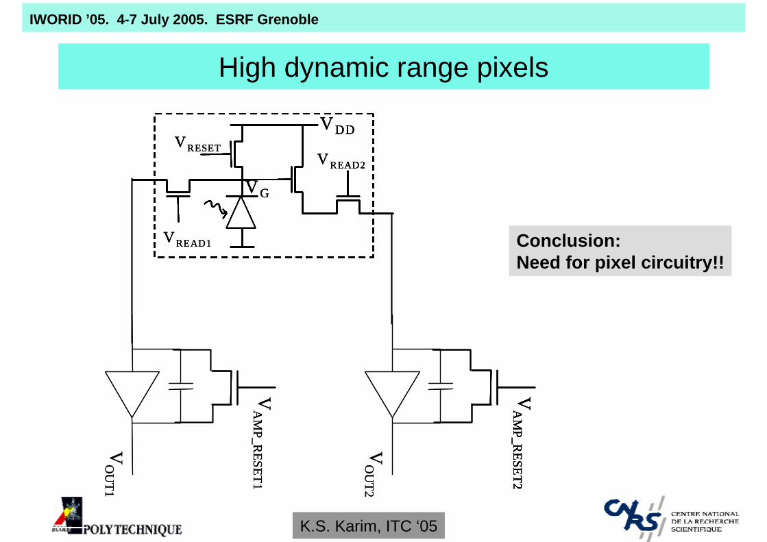
High dynamic range pixels
VRESETV READ2
VREAD1
VG
VDD
VO
UT1
VA
MP_R
ESET1
VO
UT2
VA
MP_R
ESET2
VRESETV READ2
VREAD1
VG
VDDVRESET
V READ2
VREAD1
VG
VDD
VO
UT1
VA
MP_R
ESET1
VO
UT2
VA
MP_R
ESET2V
AM
P_RESET2
K.S. Karim, ITC ‘05
Conclusion:Need for pixel circuitry!!
D. Pribat
IWORID ’05. 4-7 July 2005. ESRF Grenoble
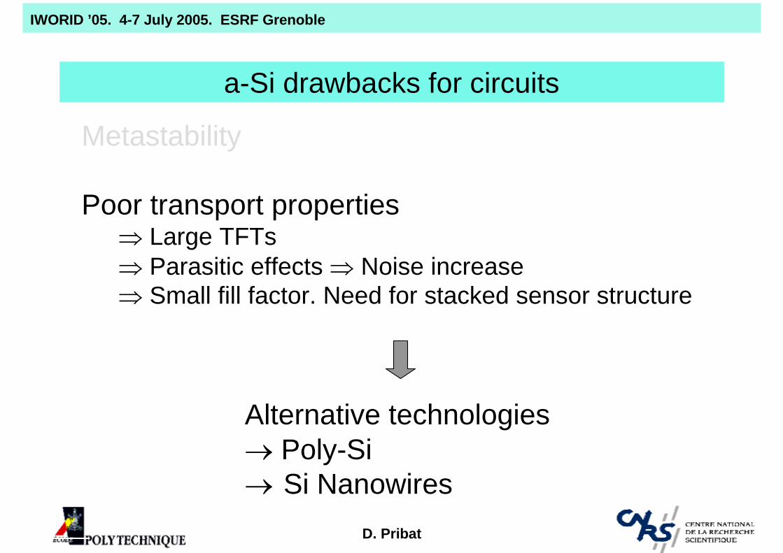
a-Si drawbacks for circuits
Metastability
Poor transport properties⇒ large TFTs⇒ parasitic effects⇒ Small fill factor. Need for stacked sensor structure
D. Pribat
IWORID ’05. 4-7 July 2005. ESRF Grenoble
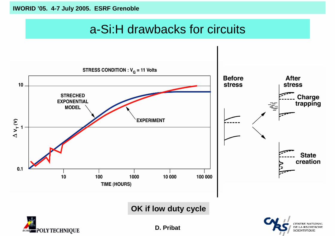
a-Si:H drawbacks for circuits
OK if low duty cycle
D. Pribat
IWORID ’05. 4-7 July 2005. ESRF Grenoble
a-Si drawbacks for circuits
Metastability
Poor transport properties⇒ Large TFTs⇒ Parasitic effects ⇒ Noise increase⇒ Small fill factor. Need for stacked sensor structure
Alternative technologies→ Poly-Si→ Si Nanowires
D. Pribat
IWORID ’05. 4-7 July 2005. ESRF Grenoble
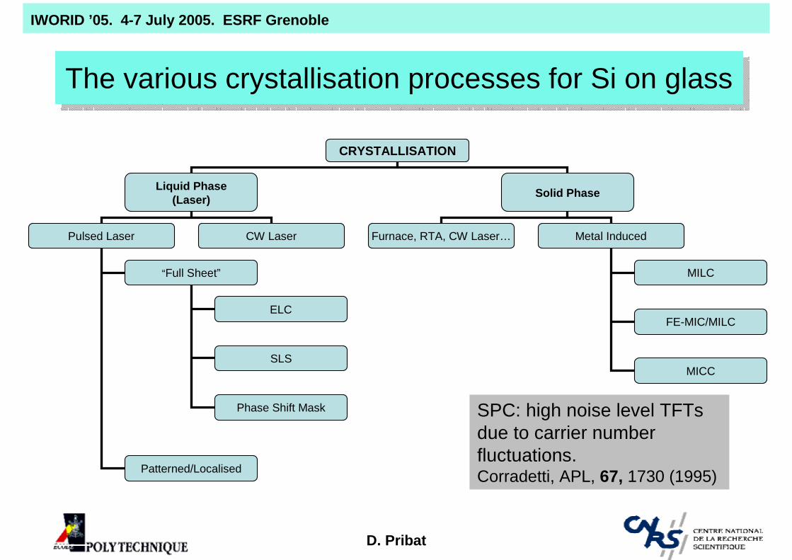
The various crystallisation processes for Si on glassThe various crystallisation processes for Si on glass
CRYSTALLISATION
Liquid Phase(Laser) Solid Phase
Furnace, RTA, CW Laser… Metal Induced
MILC
FE-MIC/MILC
MICC
Pulsed Laser CW Laser
“Full Sheet”
ELC
SLS
Phase Shift Mask
Patterned/Localised
SPC: high noise level TFTsdue to carrier number fluctuations.Corradetti, APL, 67, 1730 (1995)

D. Pribat
IWORID ’05. 4-7 July 2005. ESRF Grenoble
Crystallisation of a-Si: pulsed laser system with line beam optics
XeClXeCl, 308 nm, 50Hz, 308 nm, 50Hz
y
x
El
TopTop--hat energy profilehat energy profile
Largest line beam (Microlas):350 mm X 250 µm
L = (Dτ)1/2
D = κ/ρCp
L ~100 nm in SiO2, for τ ~25 ns
D. Pribat
IWORID ’05. 4-7 July 2005. ESRF Grenoble
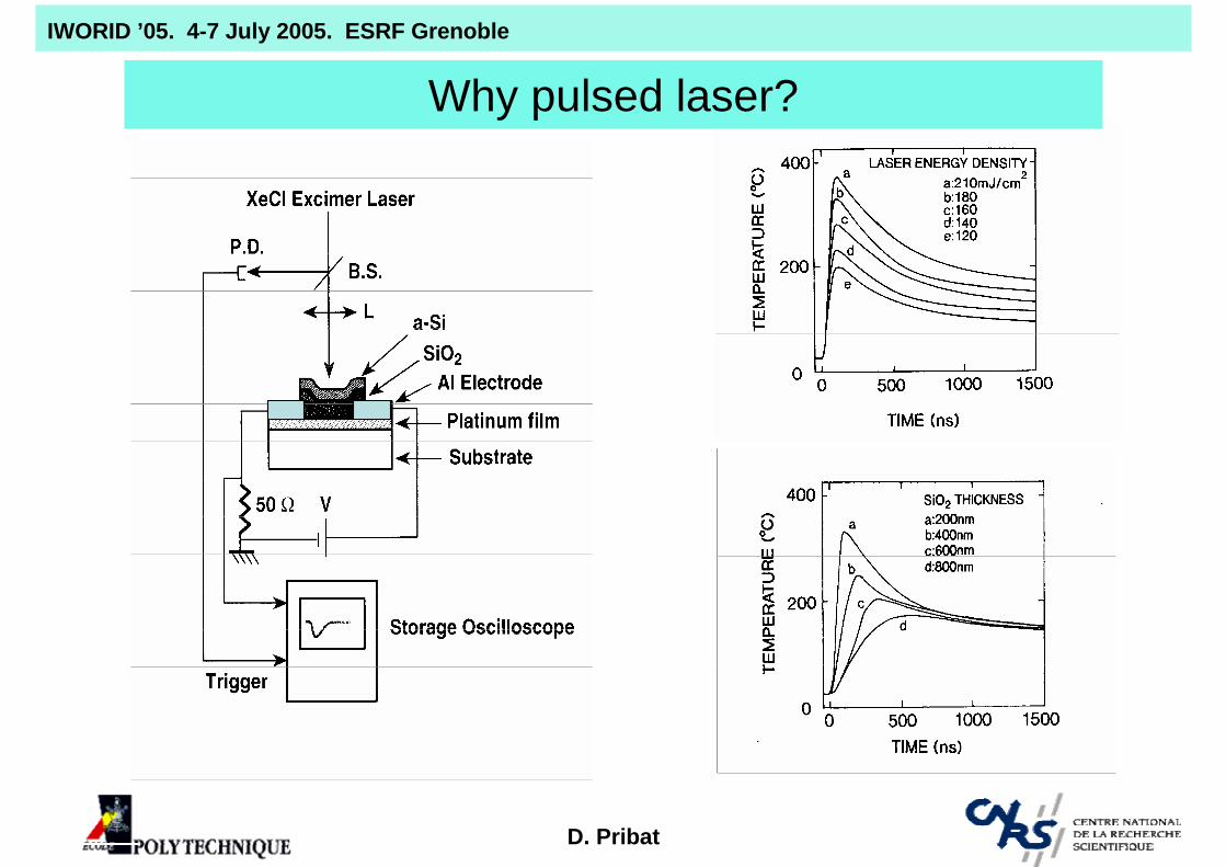
Why pulsed laser?

D. Pribat
IWORID ’05. 4-7 July 2005. ESRF Grenoble
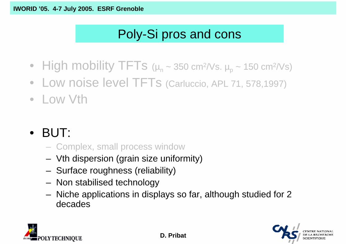
Poly-Si pros and cons
• High mobility TFTs (µn ~ 350 cm2/Vs. µp ~ 150 cm2/Vs)
• Low noise level TFTs (Carluccio, APL 71, 578,1997)
• Low Vth• Self-aligned TFTs
• BUT:– Complex, small process window for high quality TFTs– Vth dispersion (grain size uniformity)– Surface roughness (reliability)– Non stabilised technology– Niche applications in displays so far, although studied for 2
decades

D. Pribat
IWORID ’05. 4-7 July 2005. ESRF Grenoble
Grain size as a function of laser energy density (1)
E = 360 mJ/cm2 E = 400 mJ/cm2
E = 430 mJ/cm2 E = 470 mJ/cm2
500 nm

D. Pribat
IWORID ’05. 4-7 July 2005. ESRF Grenoble
cc(( µµ
m)
m)
Laser energy density (a.u.)Laser energy density (a.u.)
Grain size as a function of laser energy density (2)
D. Pribat
IWORID ’05. 4-7 July 2005. ESRF Grenoble
Poly-Si pros and cons
• High mobility TFTs (µn ~ 350 cm2/Vs. µp ~ 150 cm2/Vs)
• Low noise level TFTs (Carluccio, APL 71, 578,1997)
• Low Vth
• BUT:– Complex, small process window– Vth dispersion (grain size uniformity)– Surface roughness (reliability)– Non stabilised technology– Niche applications in displays so far, although studied for 2
decades
D. Pribat
IWORID ’05. 4-7 July 2005. ESRF Grenoble
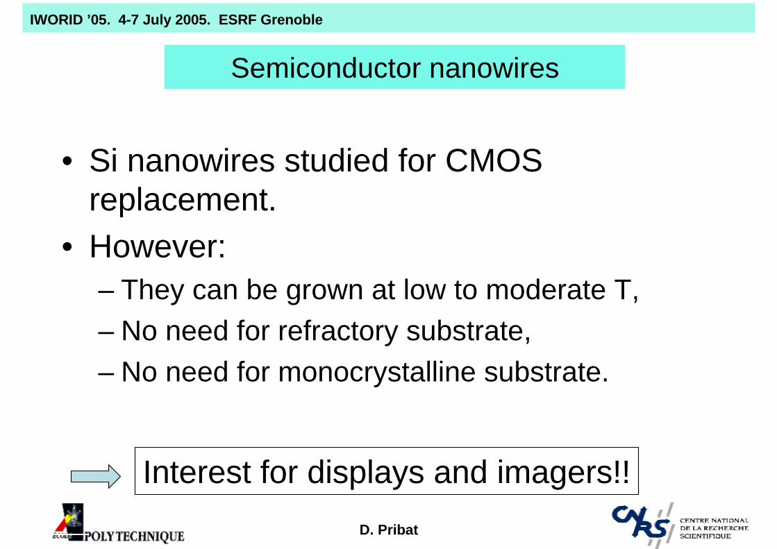
Semiconductor nanowires
• Si nanowires studied for CMOS replacement.
• However:– They can be grown at low to moderate T,– No need for refractory substrate,– No need for monocrystalline substrate.
Interest for displays and imagers!!

D. Pribat
IWORID ’05. 4-7 July 2005. ESRF Grenoble
Vapor:SiH4,
or SiH4 + PH3 or B2H6
Au-SiLiquid alloy
substrate
SingleCrystal
SiWhisker
vapor
Principle of the VLSGrowth method:
Synthesis of NWs
T ~ 400°C
D. Pribat
IWORID ’05. 4-7 July 2005. ESRF Grenoble
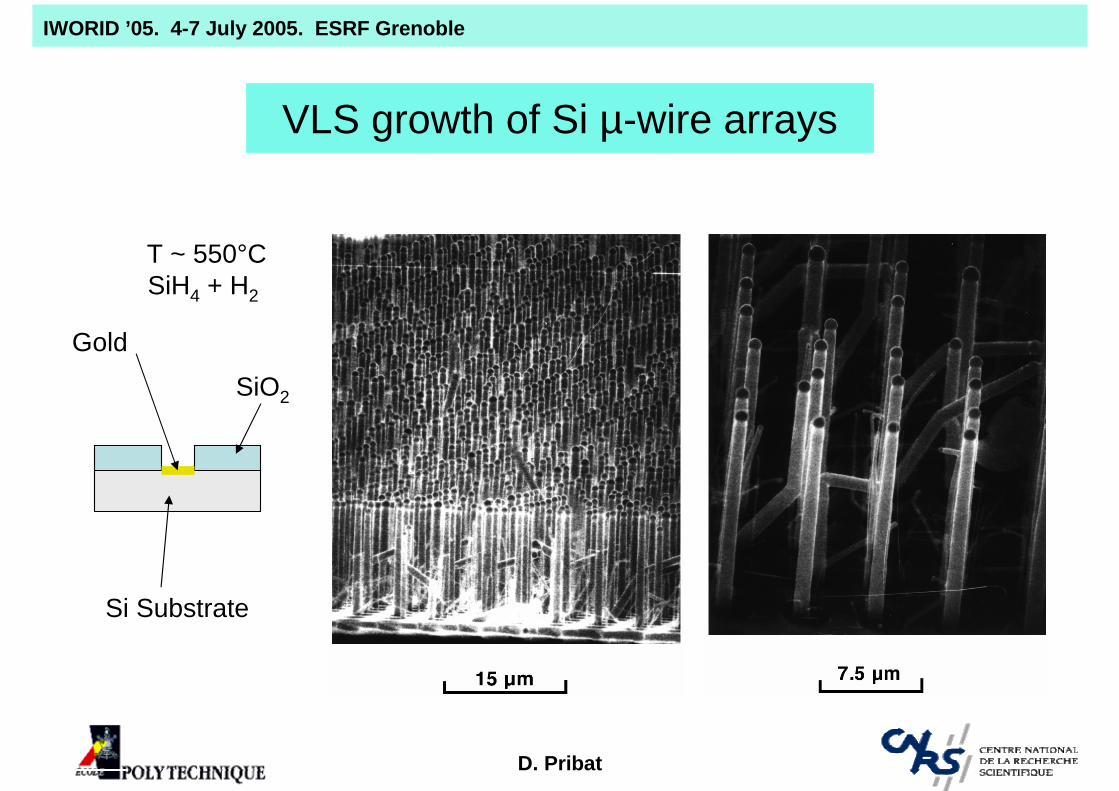
VLS growth of Si µ-wire arrays
Si Substrate
Gold
SiO2
T ~ 550°CSiH4 + H2

D. Pribat
IWORID ’05. 4-7 July 2005. ESRF Grenoble
Si NanoWire FET
µ ~ 1350 cm2/VsLieber, Nano Lett., 2003
D. Pribat
IWORID ’05. 4-7 July 2005. ESRF Grenoble
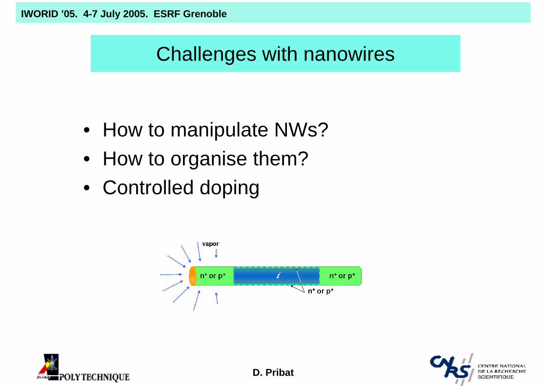
Challenges with nanowires
• How to manipulate NWs?• How to organise them?• Controlled doping
D. Pribat
IWORID ’05. 4-7 July 2005. ESRF Grenoble
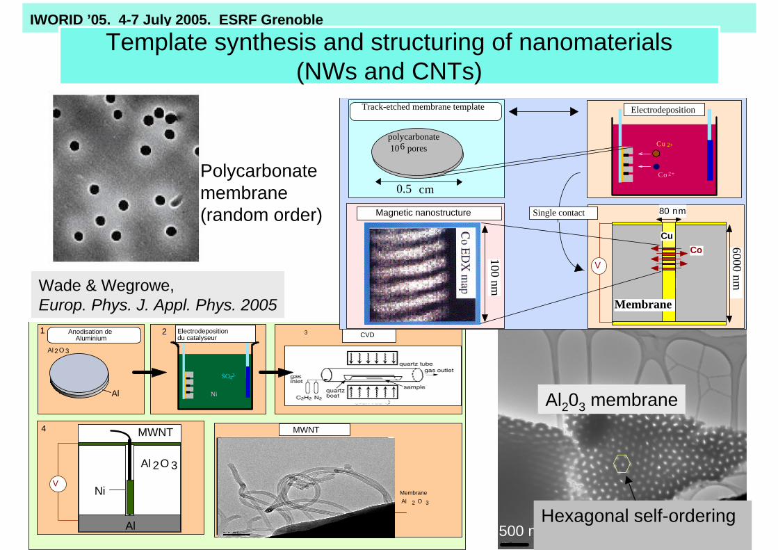
500 nm500 nm
nanotubes de carbone par CVD dans les membranes d’Aluminium anodisées
Al 2O 3
Anodisation de Aluminium
SO42-
Ni
Electrodeposition du catalyseur
2
V
4
Al 2O 3
MWNT
Ni
Al
CVD
Al
1
MWNT
3
Membrane Al 2 O 3
0.5 cm
polycarbonate
106 pores
Co 2+
Cu 2+
Electrodeposition
Template synthesis
Magnetic nanostructure
100 nm
Co
Cu
6000 nm
80 nm
Cu
V
Track-etched membrane template
Membrane
Single contact
Template synthesis and structuring of nanomaterials(NWs and CNTs)
Hexagonal self-ordering
Al203 membrane
Polycarbonatemembrane(random order)
Wade & Wegrowe, Europ. Phys. J. Appl. Phys. 2005
D. Pribat
IWORID ’05. 4-7 July 2005. ESRF Grenoble
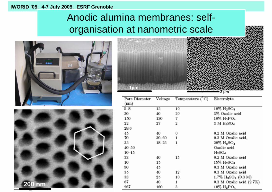
1µm1µm
200 nm
Anodic alumina membranes: self-organisation at nanometric scale
D. Pribat
IWORID ’05. 4-7 July 2005. ESRF Grenoble
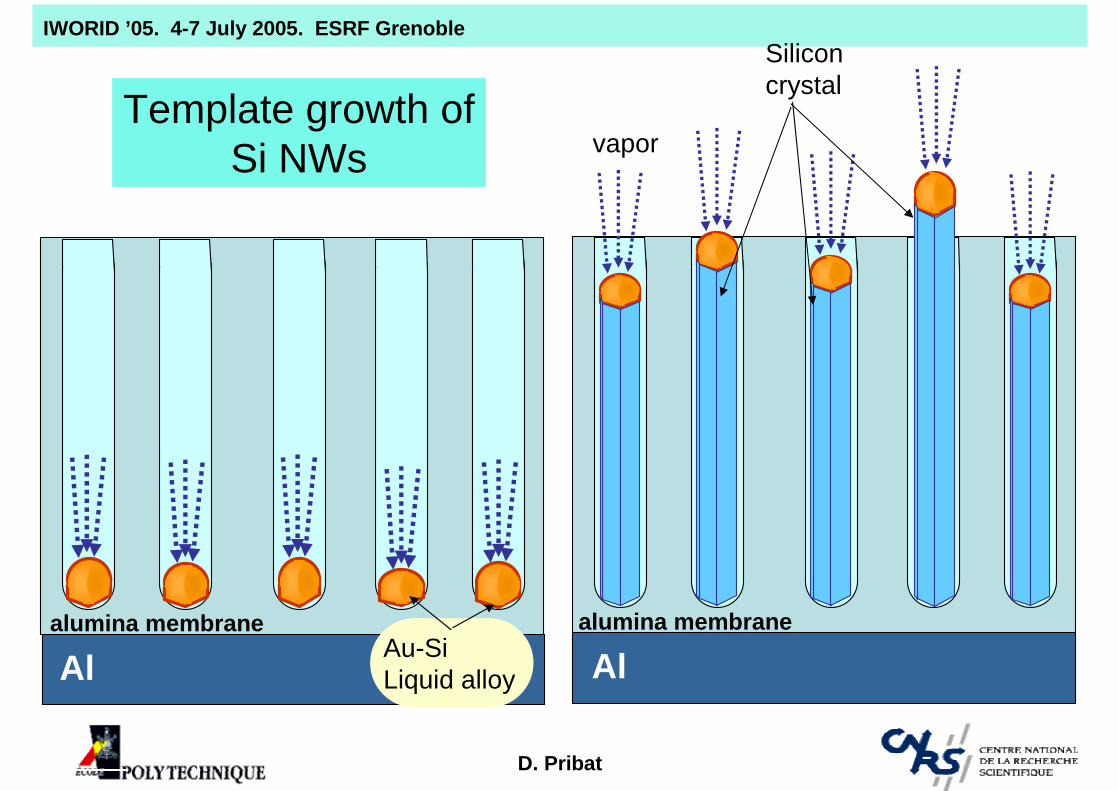
Au-SiLiquid alloyAl
alumina membrane
Siliconcrystal
vapor
alumina membrane
Al
Template growth ofSi NWs
D. Pribat
IWORID ’05. 4-7 July 2005. ESRF Grenoble
3 0 0 4 0 0 5 0 0 6 0 0 7 0 0
6 0 5 cm -14 1 3 .5 cm -1
5 1 7 .3 cm -1
inte
nsity
(a.u
.)R A M A N s h ift (c m -1)
2 92 cm -1
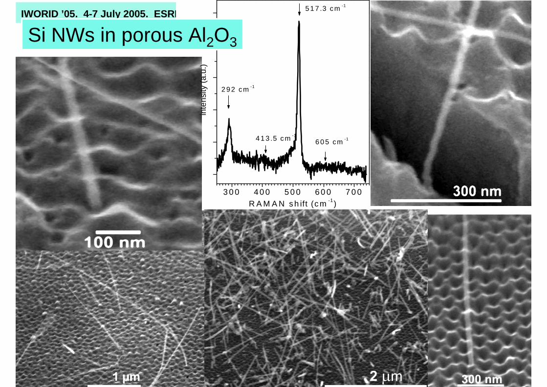
Si NWs in porous Al2O3
D. Pribat
IWORID ’05. 4-7 July 2005. ESRF Grenoble
1µm
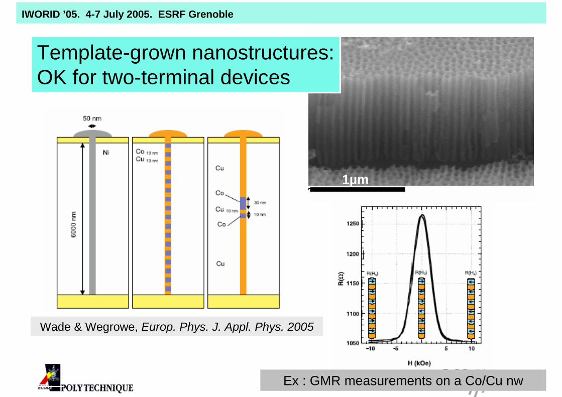
Template-grown nanostructures:OK for two-terminal devices
Ex : GMR measurements on a Co/Cu nw
Wade & Wegrowe, Europ. Phys. J. Appl. Phys. 2005
D. Pribat
IWORID ’05. 4-7 July 2005. ESRF Grenoble
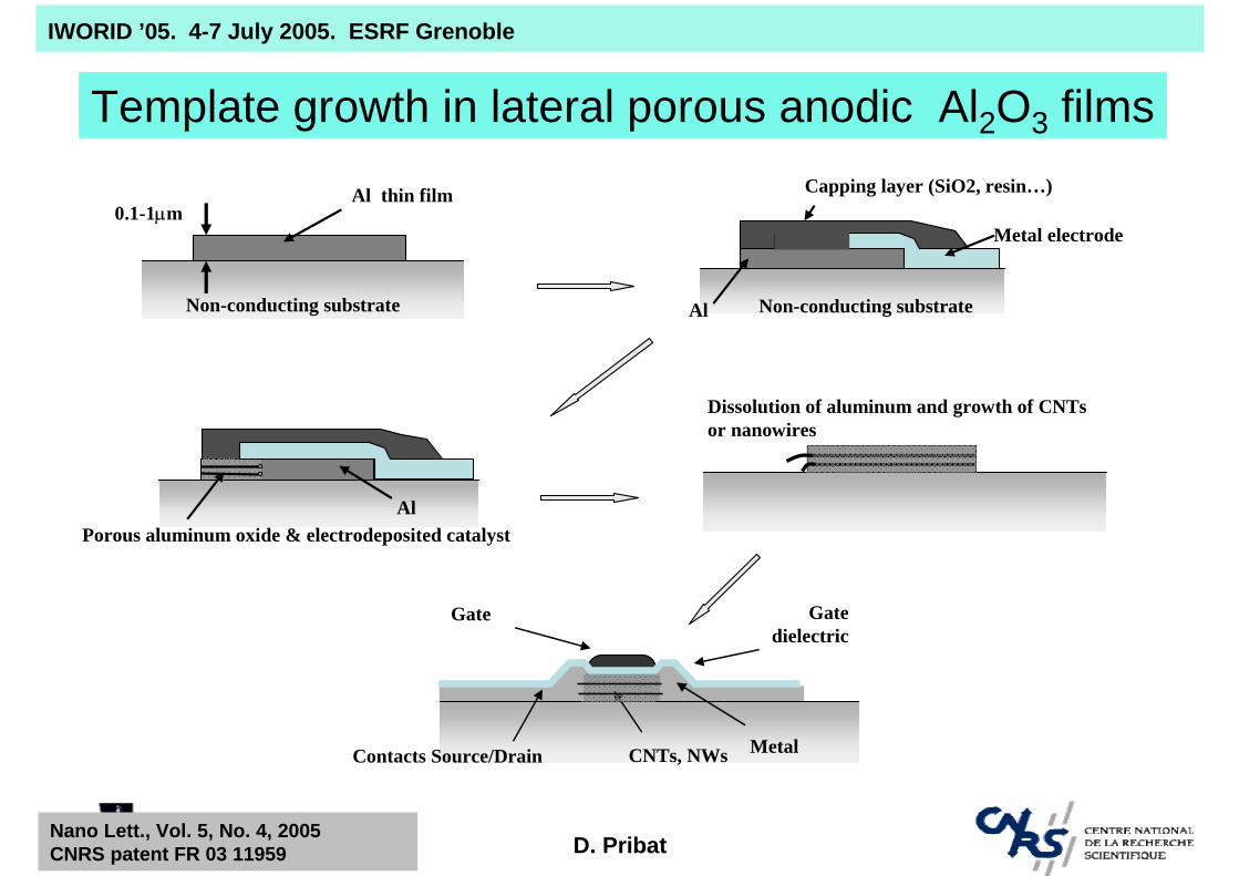
Non-conducting substrate
Al thin film0.1-1µm
Non-conducting substrateAl
Metal electrode
Capping layer (SiO2, resin…)
Al Porous aluminum oxide & electrodeposited catalyst
Dissolution of aluminum and growth of CNTsor nanowires
Gate
MetalCNTs, NWsContacts Source/Drain
Gatedielectric
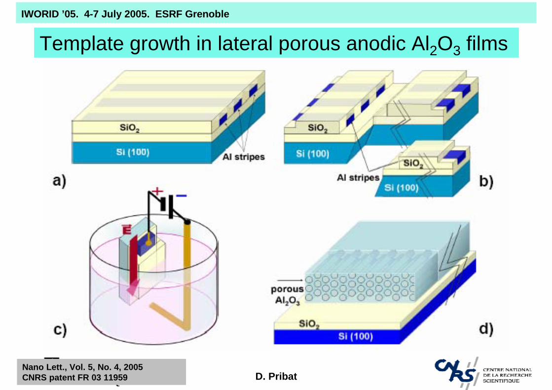
Template growth in lateral porous anodic Al2O3 films
Nano Lett., Vol. 5, No. 4, 2005CNRS patent FR 03 11959
D. Pribat
IWORID ’05. 4-7 July 2005. ESRF Grenoble
Template growth in lateral porous anodic Al2O3 films
Nano Lett., Vol. 5, No. 4, 2005CNRS patent FR 03 11959
D. Pribat
IWORID ’05. 4-7 July 2005. ESRF Grenoble
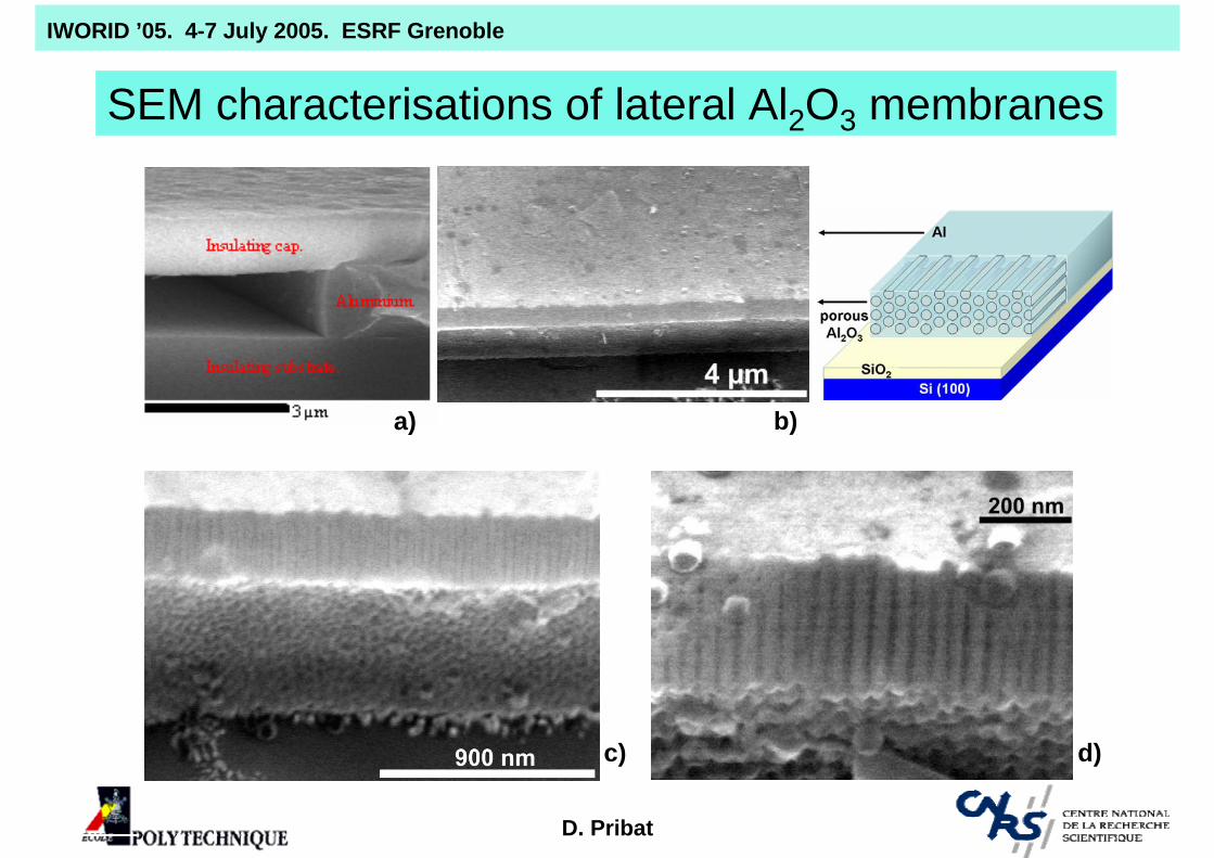
a) b)
c) d)
SEM characterisations of lateral Al2O3 membranes
D. Pribat
IWORID ’05. 4-7 July 2005. ESRF Grenoble
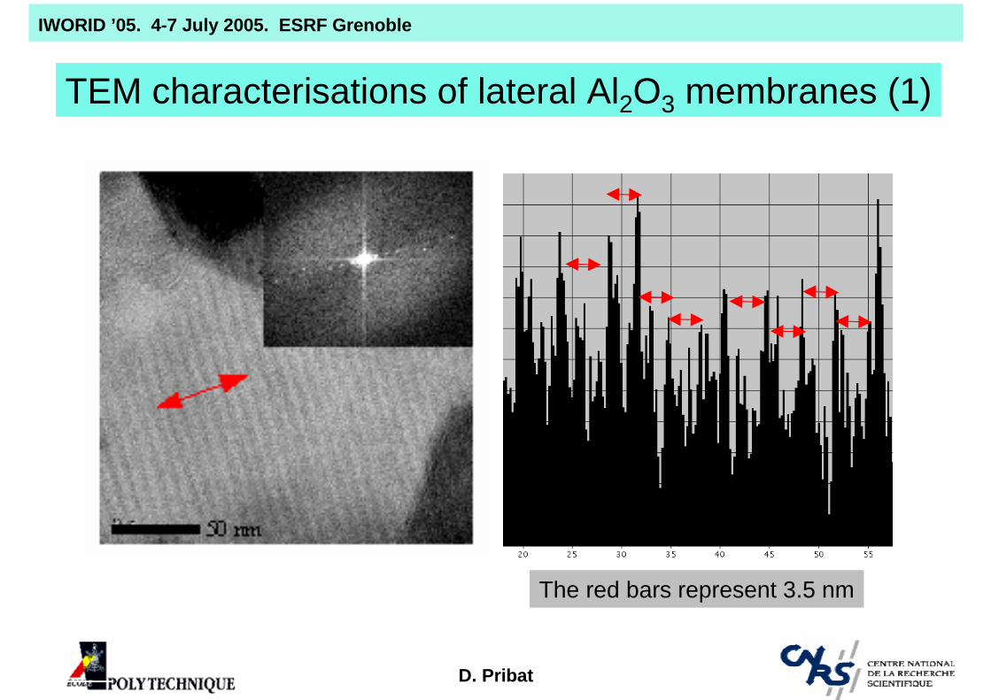
TEM characterisations of lateral Al2O3 membranes (1)
The red bars represent 3.5 nm
D. Pribat
IWORID ’05. 4-7 July 2005. ESRF Grenoble
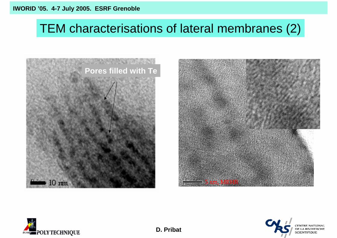
TEM characterisations of lateral membranes (2)
5 nm, MEHR
Pores filled with Te
D. Pribat
IWORID ’05. 4-7 July 2005. ESRF Grenoble
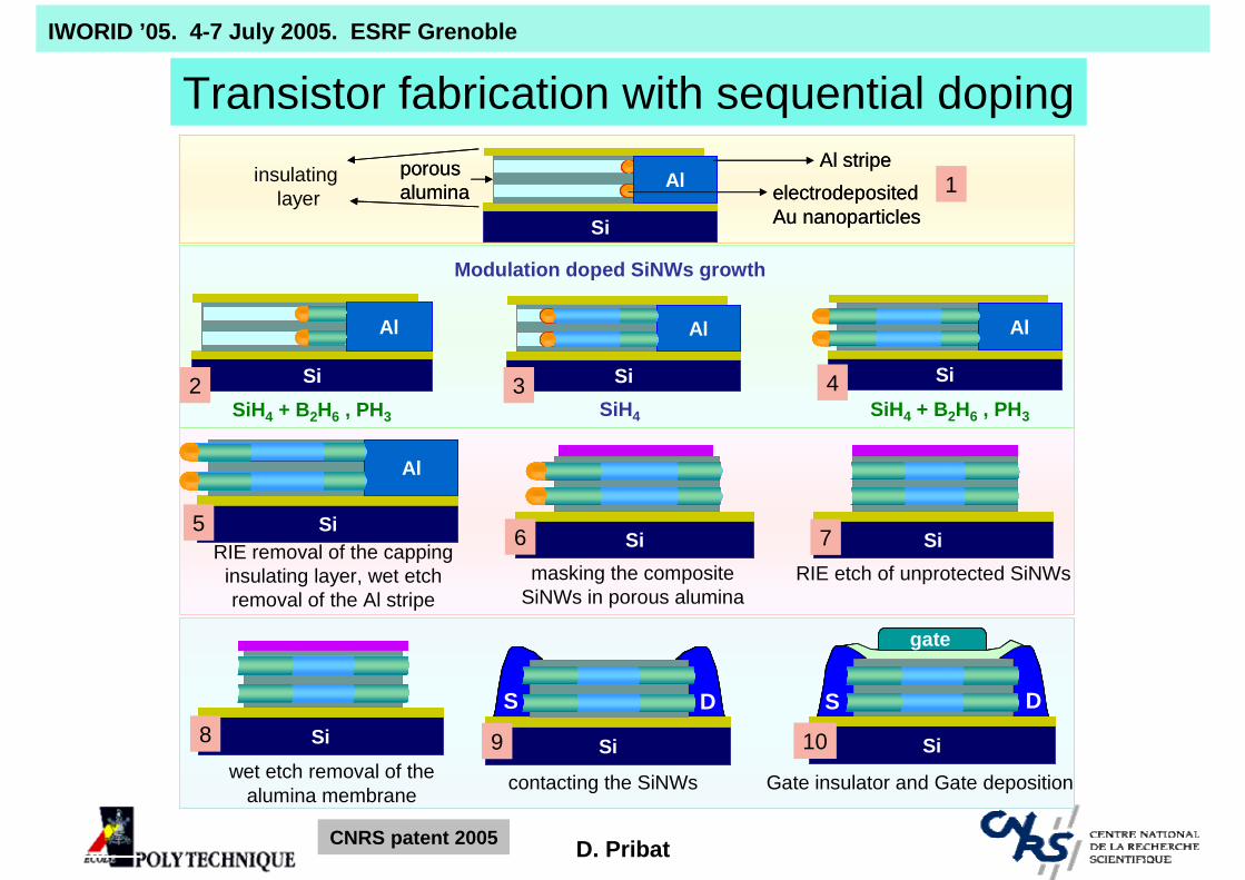
Si
Al
Si
Al
Si
Al
Si
AlAl stripe
electrodeposited Au nanoparticles
porous alumina
insulating layer
Modulation doped SiNWs growth
SiH4 + B2H6 , PH3 SiH4 + B2H6 , PH3SiH4
RIE removal of the capping insulating layer, wet etch removal of the Al stripe
masking the composite SiNWs in porous alumina
RIE etch of unprotected SiNWs
wet etch removal of the alumina membrane contacting the SiNWs Gate insulator and Gate deposition
Si Si
Si Si
S D
Si
S D
gate
Si
Al
1
2 3 4
5 6 7
8 9 10
Si
Al
Si
Al
Si
Al
Si
Al
Si
Al
Si
Al
Si
Al
Si
AlAl stripe
electrodeposited Au nanoparticles
porous alumina
Si
Al
Si
AlAl stripe
electrodeposited Au nanoparticles
porous alumina
insulating layer
Modulation doped SiNWs growth
SiH4 + B2H6 , PH3 SiH4 + B2H6 , PH3SiH4
RIE removal of the capping insulating layer, wet etch removal of the Al stripe
masking the composite SiNWs in porous alumina
RIE etch of unprotected SiNWs
wet etch removal of the alumina membrane contacting the SiNWs Gate insulator and Gate deposition
SiSiSiSi SiSiSiSiSi
SiSiSi Si
S D
Si
S D
SiSiSi
S D
Si
S D
gate
Si
S D
gate
SiSiSi
S D
gate
Si
Al
Si
Al
Si
Al
Si
Al
1
2 3 4
5 6 7
8 9 10
Transistor fabrication with sequential doping
CNRS patent 2005
D. Pribat
IWORID ’05. 4-7 July 2005. ESRF Grenoble
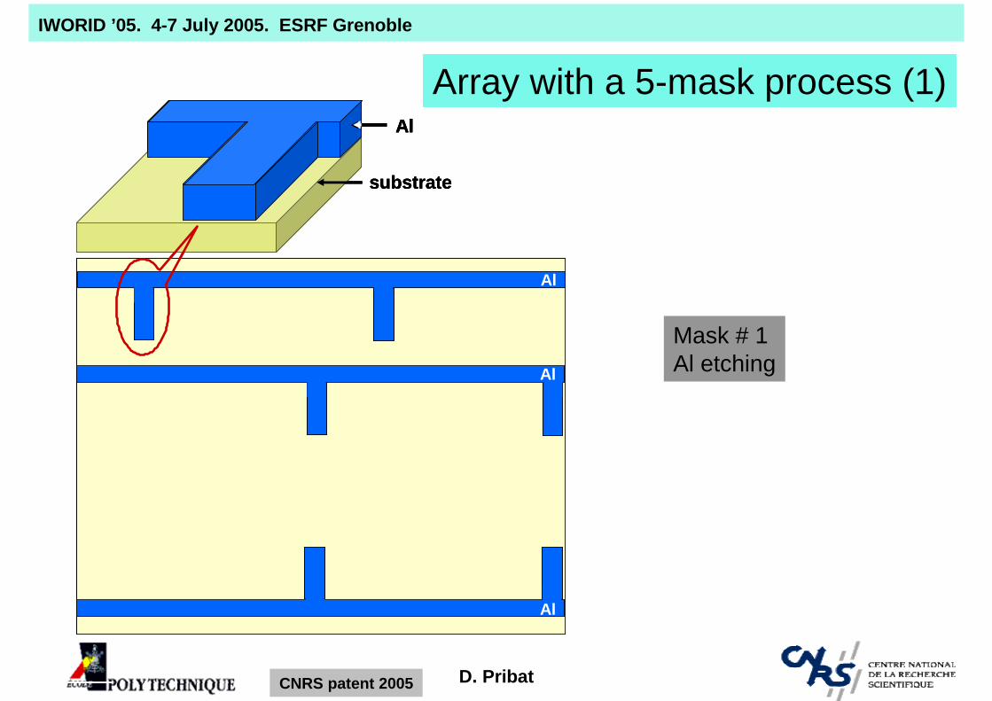
substrate
Al
Al
Al
Al
substrate
Al
Al
Al
Al
substrate
AlAl
Al
Al
Al
Al
Al
Al
Mask # 1Al etching
Array with a 5-mask process (1)
CNRS patent 2005

D. Pribat
IWORID ’05. 4-7 July 2005. ESRF Grenoble
Al
Al
Al
Al
SiO2
Porous alumina
Al
SiO2
Al
Al
Al
Al
AlAl
SiO2
Porous aluminaPorous alumina
AlAl
SiO2
Al
SiO2 deposition+
Mask # 2+
Anodic oxidation+
Catalyst electrodep.
Array with a 5-mask process (2)
CNRS patent 2005

D. Pribat
IWORID ’05. 4-7 July 2005. ESRF Grenoble
Al
Al
Al
Al Al
SiH4 + B2H6 , PH3 SiH4 + B2H6 , PH3SiH4
Al
Al
Al
Al
Al Al
SiH4 + B2H6 , PH3 SiH4 + B2H6 , PH3SiH4
Al
TFT realisationin one pump down
Array with a 5-mask process (3)
CNRS patent 2005
D. Pribat
IWORID ’05. 4-7 July 2005. ESRF Grenoble
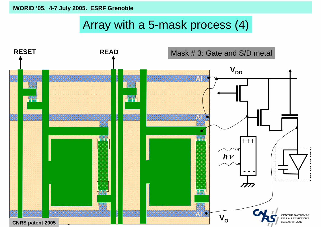
Al
Al
Al
VDD
+++
hν
VO
RESET READ
- - -
Mask # 3: Gate and S/D metal
Array with a 5-mask process (4)
CNRS patent 2005

D. Pribat
IWORID ’05. 4-7 July 2005. ESRF Grenoble
Al
Al
Al
VDD
+++
hν
VO
RESET READ
- - -
SiO2 deposition + mask 4
Array with a 5-mask process (5)
CNRS patent 2005
D. Pribat
IWORID ’05. 4-7 July 2005. ESRF Grenoble
Al
Al
Al
VDD
+++
hν
VO
RESET READ
- - -
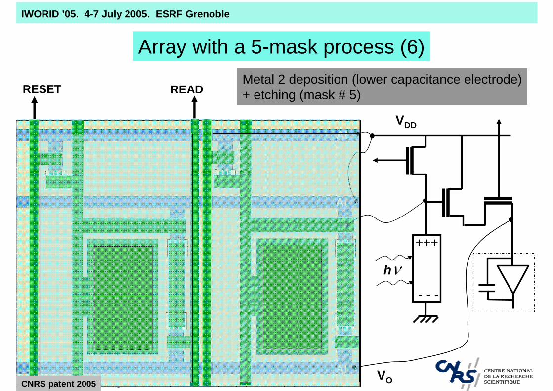
Metal 2 deposition (lower capacitance electrode)+ etching (mask # 5)
Array with a 5-mask process (6)
CNRS patent 2005
D. Pribat
IWORID ’05. 4-7 July 2005. ESRF Grenoble
Al
Al
Al
VDD
+++
hν
VO
RESET READ
- - -
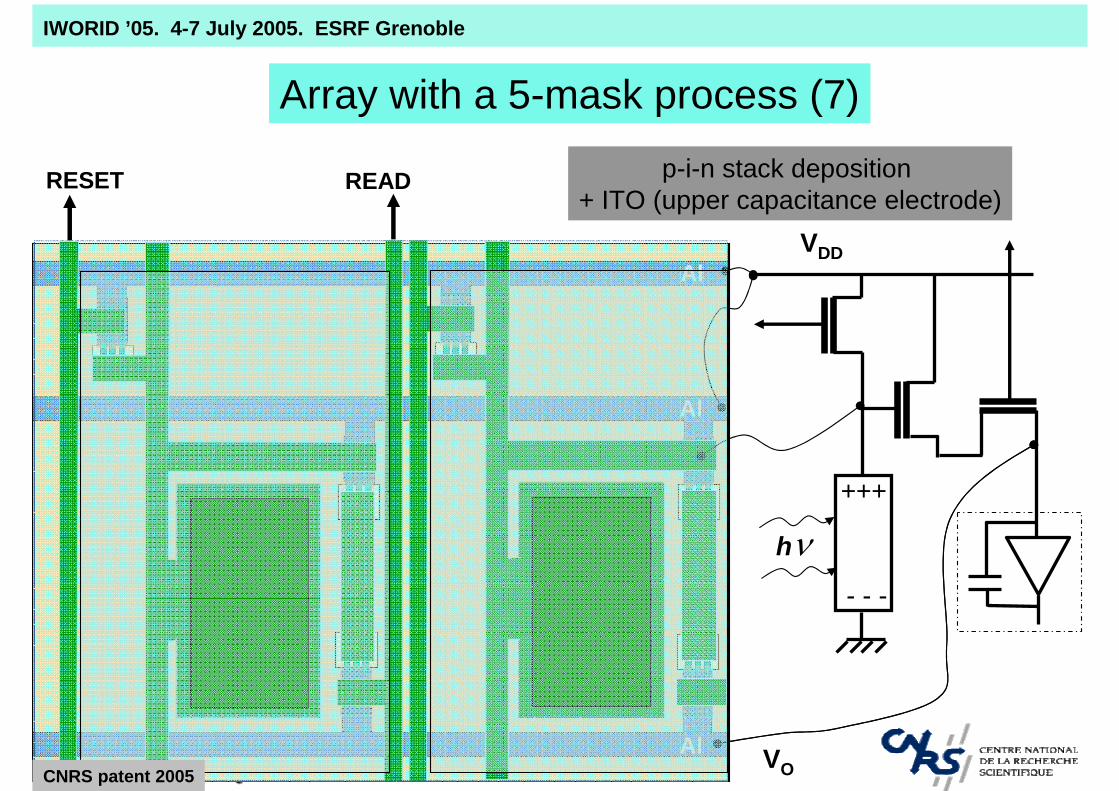
p-i-n stack deposition + ITO (upper capacitance electrode)
Array with a 5-mask process (7)
CNRS patent 2005

D. Pribat
IWORID ’05. 4-7 July 2005. ESRF Grenoble
Conclusions
• a-Si:H-based imagers present a number of advantages– Large size, high resolution, high image quality– Electronic picture handling– Compactness– Synergy with AMLCD industry (equipment, technologies…)– ….
• Need for added pixel complexity– a-Si:H limitations
• Alternative technologies– Poly-Si: complex (laser), not mature. Niche applications in
displays– Si NWs: simple, only CVD. Currently being developed
D. Pribat
IWORID ’05. 4-7 July 2005. ESRF Grenoble