Embed Size (px)
Citation preview
WL-TR-93-1103
COLOR HEAD DOWN DISPLAY PROGRAM
AD-A274 807 A,
D. L. JOSE, A. C. IPRI AND R. G. STEWART
DAVID SARNOFF RESEARCH CENTER D T ICCN 5300 -50 ELECTEPRINCETON, NJ 08543-5300 JAN2 1 1994 LJAPRIL 1993 CFINAL REPORT FOR 09/01/88-03/01/93
APPROVED FOR PUBLIC RELEASE; DISTRIBUTION IS UNLIMITED.
.S(j 94-01805
AVIONICS DIRECTORATEWRIGHT LABORATORYAIR FORCE MATERIEL COMMANDWRIGHT PATTERSON AFB OH 45433-7409
.94 1 079

NOTICE
When Government drawings, specifications, or other data are used forany purpose other than in connection with a definitely Government-relatedprocurement, the United States Government incurs no responsibility or anyobligation whatsoever. The fact that the government may have formulated orin any way supplied the said drawings, specifications, or other data, is notto be regarded by implication, or otherwise in any manner construed, aslicensing the holder, or any other person or corporation; or as conveyingany rights or permission to manufacture, use, or sell any patented inventionthat may in any way be related thereto.
This report is releasable to the National Technical Information Service(NTIS). At NTIS, it will be available to the general public, includingforeign nations.
This technical report has been reviewed and is approved for publica-tion.
ROBERT MICHAELS, Project Engineer DARREL G. HOPPER,Cockpit Avionics Office Cockpit Avionics OfficeAvionics Directorate Avionics Directorate
CHARLES H. KRUEGER, ChiefSystem Avionics DivisionAvionics Directorate
If your address has changed, if you wish to be removed from our mailinglist, or if the addressee is no longer employed by your organization pleasenotify WL/ .__ wpAFB, OH 45433-7409 to help us maintain a currentmailing list.
Copies of this report should not be returned unless return is required bysecurity considerations, contractual obligations, or notice on a specificdocument.
Fioom AppoviedREPORT DOCUMENTATION PAGE oIB W 0o704o0o81
Pul r g for this collection informatn is estimated to a 1 hoir pe. rese. ncluding the timne for reewing. instructions. searching etn data sources.gaternge nd mai ntaining the data needled and completng andreie wing the collecton o, informatio. Send commenms regarding thi burden esutimae or any othe aspect of thic*a = of infO1r1main. 1 n1cludig suggeso for rdung this burden. to Wastiton 1,4eadQuarters Servfca Directorate or Information Operations and Report 121 j nDavis 0ihway. Sude 1204. Arlingtn. VA 22202-4302. and tO the Office of Management and Budget. Paperwork Reduction Project (070441W). Washington, OC 2M003.
1. AGENCY USE ONLY (Leave blank) 2. RE PORT DATE | 3. REPORT TYPE AND DATES COVEREDAPR 1993 1 FINAL 09/01/88--03/01/93
4. TITLE AND SUBTITLE •.•u• • LPJW1 JI.•L"J.*:L-AJ'JZA•'3 S. FUNDING NUMBERSC F33615-88-C-1825
PE 63109PR 2734
6. AUTHOR(S) TA 01D. L. JOSE, A. C. IPRI AND R. G. STEWART WU 45
7. PERFORMING ORGANIZATION NAME(S) AND ADORESS(ES) S. PERFORMING ORGANIZATION
REPORT NUMBER
DAVID SARNOFF RESEARCH CENTERCN 5300PRINCETOA, NJ 08543-5300
9. SPONSORING/MONITORING AGENCY NAME(S) AND ADDRESS(ES) 10. SPONSORING /MONITORINGAVIONICS DIRECTORATE AGENCY REPORT NUMBER
WRIGHT LABORATORY WL-TR-93-1103AIR FORCE MATERIEL COMMANDWRIGHT PATTERSON AFB OH 45433-7409
11. SUPPLEMENTARY NOTES
12s. DISTRIBUTIONIAVAILABILITY STATEMENT 12b. DISTRIBUTION CODEAPPROVED FOR PUBLIC RELEASE; DISTRIBUTION ISUNLIMITED.
13. ABSTRACT (Maximum 200 words)The purpose of the CHDD program was to develop a large-area AMLCD for cockpit appli-cations. A 4- x 8-in. polysilicon AMLCD with 320,000 display cells was designedwith integrated scanners and fabricated. A support electronics system was construct-ed that accepted multisource RGB video. This system reformatted the video informa-tion to drive the display at 180 fields/second and synchronized the display to acolor sequential backlight. Moving the color information into the temporal domain,maintained the color pixel density identical to the cell density.
A 192 x 192 pixel active matrix circuit with integrated drive and scan functions wasfabricated in thin-film single-crystal silicon, using standard IC processing, andsubsequently placed on glass to form a transmissive ANLCD. The first assembled2.5- x 2.5-in. monochrome display shows greater than 85 percent pixel functionality.The speed, low leakage current, and high drive capability of single-crystal silicondevices should allow the fabrication of displays with integrated system-levelperipheral circuitry, high pixel density, and improved contrast and optical aperatureratios.14. SUBJECT TERMS Color head down display (CHDD), active matrix 15. NUMBER OF PAGES
liquid crystal display (AMLCD), thin film transistor (TFT), color 67sequential backlight, integrated scanners, single-crystal silicon 16. PRICE CODE
17. SECURITY CLASSIFICATION 18. SECURITY CLASSIFICATION 19. SECURITY CLASSIFICATION 20. LIMITATION OF ABSTRACTOF REPORT OF THIS PAGE OF ABSTRACT
UNCLASSIFIED UNCLASSIFIED UNCLASSIFIED ULNSN 7540-01-280-5500 Standard Form 298 (Rev. 2-89)
Prescribed by ANSI Std. Z39-18298-102
Table of Contents
S* par
L CHDD SUMMARY ......................................................................... 1
2. INTRODUCTION AND ACCOMPLISHMENTS ...................... 22.1. Background .............................................. ... .............. 222. Color Head Down Display System Concept .......................... 22.3. Accohplismnts............................................................... 3
3. DISPLAY DESIGN ....................................... ... ... .................... 53.1. General ......................... .................................................. 53.2. Display Circuit Operation ...................................................... 73.3. Data Scanner ........................................................................... 93.4. Select Scanner ............................ 103.5. D/A Conversion............................. .10
4. PROCESSING ................................................................................ 124.1. Process Flow ......................................................... . .............. 124.2. Fabrication and Test Equipment Upgrades .............................. 144.3. Polysilicon Process Yield Charactersts ................................ 154.4. Yield Estimates for LAF TFr Plate Fabrication ...................... 22
S. DISPLAY SYSTEM .................................................................... 29
5.1. General . ...............-.................................................................. 295.2. Support Electronics System ................................................... 295.3. Liquid Crystal Display ............................................................. 325.4. Color Sequential Backlight ..................................................... 34
6. SILICON TRANSFER PROGRAM SUMMARY ..................... . 466.1. Introduction ............................................................................ 466.2. Thin-Film x-Si Materials ........................................................ 476.3. Display Fabrication ................................................................ 486.4. x-Si-on-Glass Device Characteristics ................................... 516.,. AMLCD Characterization ....................................................... 53
7. REFERENCES .............................................................................. 58
'I1
List of Ftiures
I. Reticle 1ayout. ..... .......... . ........... ... ..... ......................... ............. 5
2. Reticl Segmenatio Diagram. ...................................................... 6
3. CHDD Layout. ................................................................... ........... 8
4. QIDD Simplified Block Diagram. . ........... ..... ........ 9
5. Data Scanner Single Stage Schematic .. ............................... 10
6. Level Shifter Schematic ... ........... ............ 10
7. First Stage Grayscale Counter Schematic ... ............................... 11
8. Polysilicon Process Flow Diagram. ............................ 139. Five-Lot Moving Average of Aluminum Shorts and OpensYield Data. .............................................. ... . ....... ...................... . ..... ..... .1.
10. Five-lot Moving Average of Active Plysilicon Shorts andOpens Yield Data ............. ....... . .. ....... 9
11. Five-Lot Moving Average of Gate Polyuilic Shorts andopens Yield Data. ....................................................................... 20
12. N- and P-Channel Transistor Threshold Voltages as aFunction of Time ................................................................... 26
13. N- and P-channel Transistor Drive Currents as a Functionof Trune ................... ...... 27
14. N- and P-Channel Leakage Currents as a Function of
'rime ............................................................. ................................. 28
15. Major Units for CHDD System. ........................ 30
16. SES General Block Diagram ......................... . . 31
17. Chopped Ramp D/A Diagram. .................................................... 32
18. Contrast Ratio Measurement. ......................................................... 33
19. Major Units for CHDD System....... ........ ...... 34
20. Video and Backlight Sequencing ..................................................... 35
21. Video and Backlight Sequencing ..................................................... 36
22. Lamp Dimming Range. .................................................................. 38
23. CIE Chromaticity Diagram. ............................................................ 39
24. Diffuser Plots .................................................................................. 40
25. Diffuser Plots ................................................................................... 41
iv
List of Figures (Cent'd.)
26. Backlight Uniformity ....................................................................... 41
27. Light Level Schedule ............................... 42
28. Colr-Sequential Experiment. ......................................................... 43
29. Color-Sequential Phosphor Emission. ... ....... . 44
30. Silicon-on-Insulator Materials Fabrication Process .................... .. .47
31. Transistor Army Fabrication Sequence ....................................... 49
32. Silicon Display Transfer Process ................................................... 50
33. Qross-Section of Transferred and Assembed AMLCD .................. 51
34. N-Channel Transistor Sub-Threshold Characteristics. .................... 52
35. Effect of Neutron Irradiation on Device BreakdownVoltage .................................................... .. .. 53
36. Photograph of World's First Silicon Transfer AMLCD .)................. 55
37. Photograph of Fully Functional Transfer AMLCDAssembled with Color Filters Center ............................................ 56
38. Photomicrograph of Individual Pixel Electrodes of a PolyDisplay (Upper Figure) and Transfer Silicon Display(Lowe Figure) Showing Absence of Diclnations in theTransferred Display ............................................................... 57
Accesion ForNTIS CRA&I
DTIC TAB QUnannounced 0Justificatio
ByDistribution I
Avdilability Codes
-Avail and/or
Dist Special
V. ..
List of Tables
Tnaba Page
1. Tabulation of Yield e Due aD FacilityUpgaes ..... ... .................... 19
2. December 1990 Test Structure Yield .............. .... 21
3. November 1992 Test Structure Yield ......................................... 21
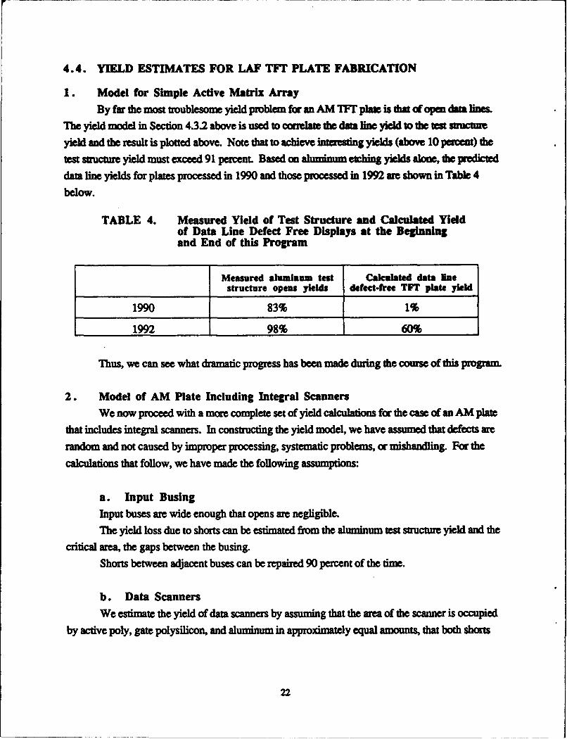
4. Measured Yield of Test Sicturm and Calculated Yield ofDam Line Defect Free Disphys at the Begnning and Endof this Program ....... .................................... 22
5. Calculated Repairable Yields of Data Lie Defect FreeDisplays and of "Nearest Neighbor Data ScannerSubstitute" Displays at the Beginning and End of thisProgranm ...................................... 24
6. Calculated Repairable Yields of Data Line Defect FreeDisplays and of "Nearest Neighbor Data ScannerSubstituted" Displays for Existing 5-Bit Design and forNew Low TFI Count Design ........................................................ 24
7. Contrast Ratio ................................................................................. 34
8. Backlight Luminance Measurements .............................................. 38
9. CIE Lamp ........................C............................... . .39
vi
r
PREFACE
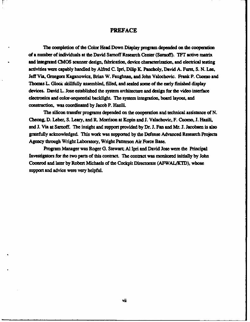
The completion of the Color Heed Down Display program depended on the cooperatimof a number of individuals at the David Sarnoff Re3each Center (Sarnoff). TFI active matrixand Integrated CMOS scanner design, fabrication, device h eriti, and electrical testingactivities wer capably handled by Alfred C. Ipri, Dilip K. Pancholy, David A. Furst, S. N. Lee,Jeff Via, Grzegorz Kaganowicz, Brian W. Faughnan, and John Valochovic. Frank P. Cuomo andThomas L Glock skillfully assembled, filled, and sealed some of the early finished displaydevices. David L. Jose established the system architecture and design for the video interfaceelectronics and color-sequential backlight. The system integration, board layout, andconstuction, was coordinated by Jacob P. Hasili
The silicon transfer programs depended on the cooperation and technical assistance of N.Cheong, D. Leber, S. Leary, and R. Morrison at Kopin and J. Valachovic, F. Cuomo, J. Hasili,and J. Via at Sarnoff. The insight and support provided by Dr. J. Fan and Mr. J. Jacobsen is alsogratefully acknowledged. This work was supported by the Defense Advanced Research ProjectsAgency through Wright Laboratory, Wright Patterson Air Force Base.
Program Manager was Roger G. Stewart; Al Ipri and David Jose were the PrincipalInvestigators for the two parts of this contract. The contract was monitored initially by JohnCoonrod and later by Robert Michaels of the Cockpit Directorat (AFWAX./KTD), whosesupport and advice were very helpful.
Vii
1. CHDD SUMMARY
"Ma primary gol of this contact was to produce a larg-area polysilkm active matrixliqid crystal disply (AMLQ)).
Ova the pas 4 years of this contzat, the con of polysilico AML plate processing hasrequired a 3 rmilon dollar cqa l ex;pem and 8 million dollars in operating costs. Thirtypecent of this operaung cost was funded under his contrct, and 70 percent was covered bycoaeiaI customers and Samoff internal funding. During this period, we have had fewer than12 full-tme support staff supporting this effort and an expendiure rate •f 2 million dollars a year.
We have learned from this expeience, that a successful AMLD fabrication facility willrequire a 20 to 100-million dollar investnent, 50 to 100 full-time sta and an expenditure rate of 5Io 10 million a year to maintain a constant throughput from the facility.
The inabiity to produce a fully functional, defect-free Color Head Down Display alsoindicates that it is beter to have a simplified display design rather than rely upon redundancy toovercome the defects
There weu three remaining problems with the color-sequential grayscale display system
First, the reduced con•tst ratio of 17:1 was primrily influenced by pixel leakage
and the combined disclnations and boundary effects in each cell
Second, the color of the color-sequential system is desanutaed due to phosphor
emission persistence of the backlight lamps, the delay in the liquid crystal response.the forementioned reduced convast ratio, and the charge redistribution of the pixel
capacitance as it is sequenced through the dthe different color fields.
The third problem is the image artifacts due to the variability of the demultiplexingof the input data.
t1
2. INTRODUCTION AND ACCOMPLISHMENTS
2.1. BACKGROUND
The David Samoff Research Center (Sanoff) has played a significant historical role in thedevelopment of flat displays. The original discovery of elecuo-optcal effects in liquid crystalnaftjd at Samoffl led to the first liquid crystal display (LCD).2 Poeering wor on matrix-
addressed displays,3 as well as research on thin-film transistors (TIfs),4 was performed here; inaddition, lr flat cathode-my tubes (CRTs) for wall TV appcatons have been emsivelystudied.5-6 Present eforts are aimed at developing active-matrix TFW LMs for high-resolution,full-color, flat, analog displays.
Sarnoff has emphasized the development of polyc ale silicon (poly-Si) WFrsdeposited on relatively inexpensive glass substrates for its active-matrix LCD program. No otheractive-matrix technology has all the critical virtues of high mobility, good stability, relativelyinepese (glass) substrate, CMOS, and high-quality ieoects. We have also developed on-plate integrated scanner circuits to eliminate the large number of intrinsically unreliable connectionsto the row and column lines of the display from external matrix-addressing drivers. Scanneddisplay devices for the present CMDD contract consist of a 400 x 800 TF1 army with an elementpitch of 0.250 mm (100 linesuln.). The integral CMOS scanners have 5-bit-wide data channels,with integrated chopped ramp digital-to-analog converters.
2.2. COLOR HEAD DOWN DISPLAY SYSTEM CONCEPT
In the Sanoff scanned displays, the twisted-nematic liquid crystal (TNC cells act as lightvalves to modulate the transmitted light from an illuminator. The basic cells exhibit an analogtransfer characteristic, which produces a continuous, mono,-nicaly decreasing brightness for the
given picture element in response to a continuous, monotonically increasing video signaL Thepoly-Si TFT scanners developed by Sarnoff have a speed capability higher than is needed fordisplay frame rates of 60 Hz.
The need for brighter and more effient mitary displays has led to the concept of a color-
sequential fluorescent backlight for the illumination of a large-area LCD. In a field-sequential colorsystem, video information for each primary color is loaded into the liquid crystal army, onecomplete color field at a time. The liquid crystal cells will synchronously modulate the light from acorresponding temporally sequenced thre-color light source. With a high enough sequencing rate,a viewer will see a full color image with a color gamut that is limited by the chromaticitycoodinates of the three color light sources. There will be no light attenuation reslting from the
2
p of a fiter, and each pictre element corresponds to a single liquid crystal cell imstead of agnrup of dmt or more cells that form a color filter pixeL This display will, dthrefore, have muchhigher brighmess and resolution than a color filter LCD for a given power input and display size.
2.3. ACCOMPLISHMENTS
Under the Color Head Down Display portion of this contract, Sarnoff has designed,constructed, and demonstrated a large-ar LCD with an analog video interface system cor-sequential backlight system. The milestones in the course of this work, have been:
"* The development of an integrated finctional tet and repair station
"• The completion of the support electronics system (SES)
"* The integration of the color-sequential backlight system
"1 The selection of either the silicide or double metal option for faster display
operation
"* The selection of internal or external display assembly locations
"• The fabrication and assembly of a 4-x 8-in plate that operates at 180-Hz field
rate
" The integration of the display, color-sequential backlight, and SES for final
demonstration.
Other accomplishments under this part of the contract have been the:
(1) Demonstration of 192 x 192 displays with 0.1-in flush seal edges
(2) First demonstration of the color-sequential backlight system
(3) LAF start-up and first successful stepper assembly of a complex circuit
(4) Successful completion of the 4-x 8-in grayscale display design
(5) Fabrication of CHDD with functioning data/select scanners
(6) Fabrication of the first 4-x 8-in display with integral black matrix
(7) Autonatic testing and yield data base
(8) Automatic testing and yield data base
3
(9) Line, parametric, and WAT yiekis over 70 percent
(10) Low resistance gates (Rho - 0.25 C•q)
(11) Low resistance N+ sourcedrain regions (Rho = 350 C•I)
(12) Combined funiconal test and repair staoon
(13) Fabrication and assembly of 4-x 8-in plate that opeaes at 180-Hz field rate
(14) Generation of 11 patent disclosumes
4
3. DISPLAY DESIGN
3.1. GENERAL
Integrion of the scanning chcutry needed to drive the 400 x 800 pixel AMLM) wasachieved by fabricating both data-line and select-line driver circuits on the 127-mm x 228.6-mmrectangular glass substmr along with the same polysilicon thin-film pixel anstors used toimprove the optical performance of the display. TIe maximnum ptcessing taperat= in thepolysilicon transistor fabrication process is kept below 6500C to prevent meltng or warpage of thelow-cost glass substrates.
Since the display IC is too large to fit within the field of even a 2:1 wafer stepper, the 125-x225-mm design must first be preassembled on a CAD wodkstation and then partitioned into 17smaller reticle segments. These segments were MEBES written onto a 7-in reticle as shown onFig. 1. The final assembly of the display was completed by programming a large-area waferstepper as shown in Fig. 2.
UNIT: uM (micr) +lInh=XZE:
mm
mmo
4 M
W /
-"-00mm •'---U.8mm -
Figure 1. Reticle Layout.
F
wpý_PjordswPlesse am NOTE
x 2 xxx
--VIP K
xx
NOTE: # I
allgnnwrvt keywW ted probeslignmerd key.
----------.. .......... .. ....... .... WP__N
rw _0 r wr-P
Figure 2. Reticle Segmentation Diagram.
6
3.2. DISPLAY CIRCUIT OPERATION
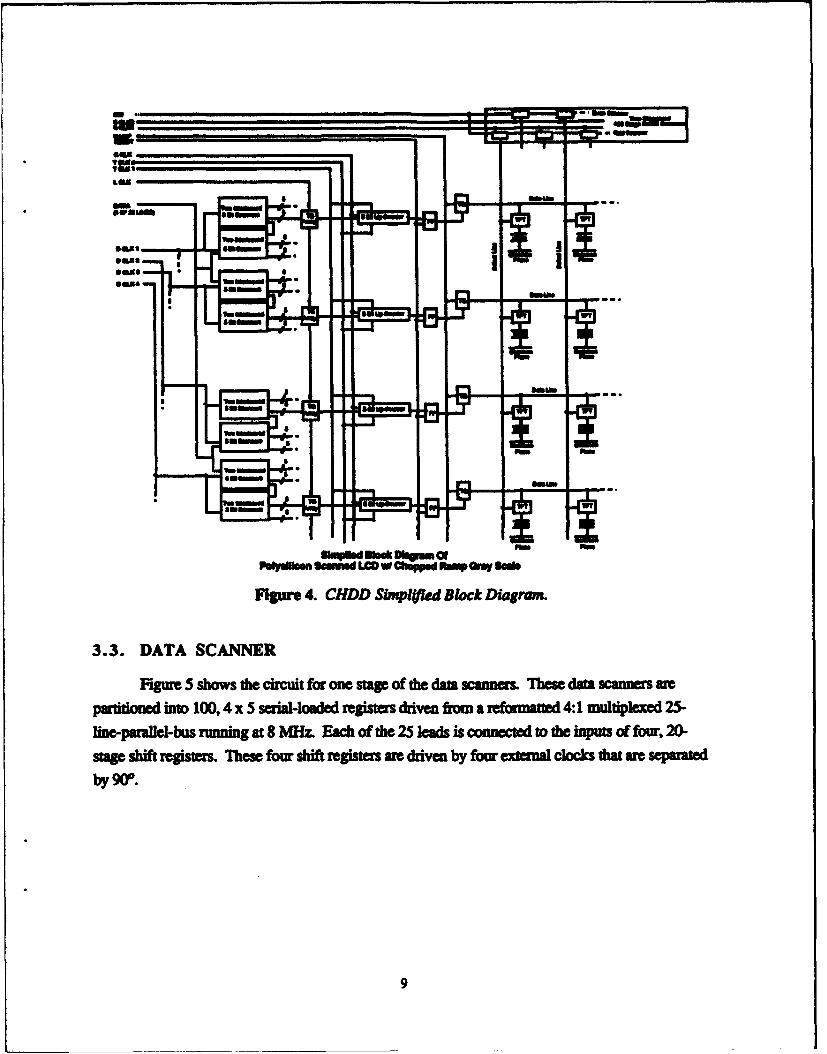
Twe scanner circuits ae implemented in dynamic CMOS circuitry. A single-dam scaner islocated at the top of army, as shown in Fig. 3. The select scanne are on the left and right. Thecircitry is divided into 54 independent blocks to increase the effectiveness of the redundancy andlaser repair procedures. Te are 25 blocks of 4 data line scanners plus 4 separate circuit blocksfor the select scanners.
Figure 4 shows the circuit block diagram for the integrated scanner display. The diagram,also shows the "Chop Ramp" scanning technique that is used to handle the 32 gray levels colordisplay requirment. Each data line is driven by a transmission gate controlled by the output of a5-bit counter. During the first line period, the 5-bit grayscale code for each pixel is loaded into thedata shift registers. At the end of the line period, the data are transferred (2000 bits at a time) fromthe shift register latches to the counters. A control-latch flip-flop is also reet to tirn on all 400transmssn gates. During the second line period, the maste dam bus is ramped by a lowinpedae driver frnm 0 V to 5 V.
The master data line ramp is always the same and no longer contains any information. Theanalog voltage presented to the data lines now depends entirely on the contents of their respectivecounters. After a short delay, the counter clock starts incrementing all of 800 data line countemWhenever each counter reaches count of 11111, it sets the control-latch flip-flop to turn off thetransmission gate. For example, if a 11111 code is loaded into data line No. 118, then itstransmission gate will remain conducting only long enough to discharge its data line completely toground. At the same time, if data line No. 122 is loaded with a 00000 code then its transmissiongate will remain conducting throughout the entire line period, allowing its data line to become fullycharged to the 5-V level. Dam lines with intermediate binary codes, such as line No. 120, will becharged to intermediate levels before their transmission gates turn off and chop or "freeze" thatparticular data line at an intermediate point on the ramp. This "Chop Ramp" scanning circuitachieves an accurate, uniform, 32-step digital-to-analog conversion.
7
Figur 3.m BounLaout
T~t euesw8
WWI
OWN=a Ime Dr IF
*ague 4. CH!Smlf BokDarm
3.3. ATA SANNEeft grnehw h icutfroesaeo tedr cnes heedt cnesm
patiine it 10, 5seil-oae rgitrsdrvn ro rfomttd : mltpexd 5line-parallel-bus rniga8 fl. ahofte2ldsico etdtoheIBM t ffor 0
stageOM sftrgsesThsforsitrgsesaedinbyforetnacokshtaesprtd
by90so
gu9w

CU ---
0CLK °
lgume S. Dat Scanner Singl Stae Schmanac.
3.4. SELECT SCANNER
An uproved voag level sidfber cruit was designed for the lect scunner cmuit Aconventional level shifer cirkit will not always function propedly with c••in poor deviceca c s and high opetng volages. As shown in Fig. 6, Ni and N2 form a cunt mmrr.When Vin -0 V, P1 is off, P2 is on, and N1 conducts no cument With no conducting currentmirmrdinN2, node"b" will bepulledup oD 15 VbyP2. When Vm -15 V, P1 ison, P2isoff,the Ni cunent will be mimred into N2, and N2 will drain the cumt at node "b" until th nodeleaches -5 V.
livOR
Ybb
av.w
FIgure 6. Level Shifter Schematic.
3.S. D/A CONVERSION
In order - -,-bieve t video rate operation, a high-speed gayscale counter is required.Figure 7 shows the first stage frequency divider circuit for this grayscale counter. By introducing
10
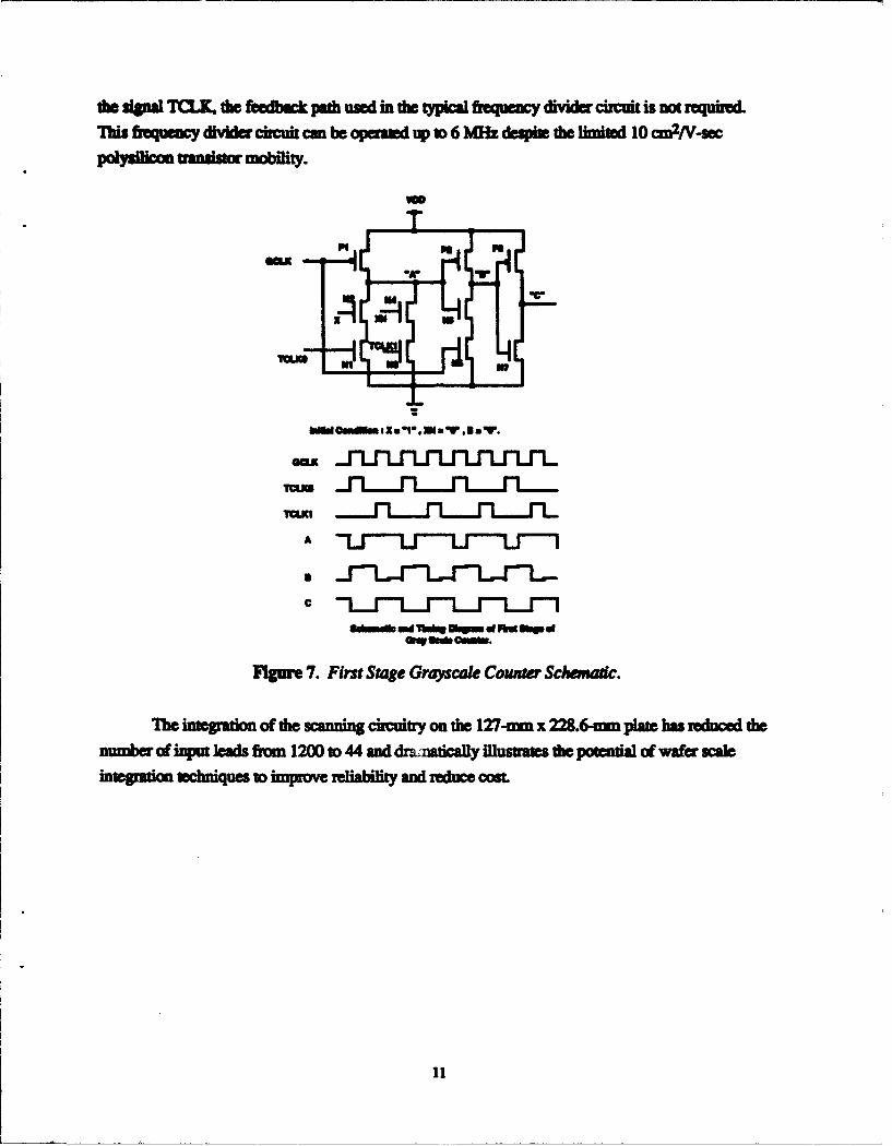
the Opgal TCX,. dke bedecbk pada used In fte tpial frequeuiy divider circuit is mc requkuL7%is frequmiY divder circuit can be opeatd up ID 6 M& de ditete limited 10 ars/N-s=
Wdcommon :XUI. S,.. U1W a.
Jrr~~ LrLrLrL
Tom
Figum 7. First Stage Grayscale Counte Schematic.
Ile imcepation of the scanning circuitry on the 127-nun x 228.6-in Plate bas reduced thenumber of input leads from 1200 to 44 and drarnazicafly Ilusrate the potetia of wafersceinegratim techniques to improve reliability and reduce cost.
4. PROCESSING
4.1. PROCESS FLOW
Nkiench-diagonal LCQs with integral scanners wer produced on 5-x 9-in rectangulaglass subsras. Both the data-line and select-line drivers circits wee fabricated simultneouslyon a 250-lam pith. The picture element (pie) army was comprised of 400 x 00 pixelcontaining polysilicon thin-fim transistors as the swirching elements. The process used 10fabricate the trasistor armay is described below.
"The pr cess flow for the fabrication of the 400 x 800 trasistor army is shown in Fig 8.The starting glass material was Hoya NA-40% which has a maIn prn es -- g tempnerature of6500C In order to use the glass at this emperatue, however, it is necessary to anneal it at varis
temperaure ad tmes to "stabilie"the glass so that subsequent high-temperature oesnstepswillnotcause movement in the glass of> 50ppm. Thealierthatusedin this prcs is capable of mnification co ntion of about 70 ppm and, hence, it isdesiible to keep the glass movement below this maximum valuve After glass anneal and cea•nnthe first silicon layer (1500 A) is deposited at a mqerature of about 5MOC. At this temperamn•uthe depoed silicon lay is essentially ampous with snmll grns located at the gU-siliconintefac Thse grains serve as nucleation sites for subsequent grain growth during later high-Jnmprsare steps.
After removal of the silicon from the display back surface, the front surface silicon layer isphotolithographically patterned and etched to form transistr islands. Next, a 750-A gate oxide isgrown at approximately 640PC. During this oxidation step, the silicon fm is completely
c0ysa ed to form a continuous layer of rains that 8 qe app•rimately 100 to 300 nm across.This rehmystallintion process is igor-ant in forming relatively large grains that produce carriermobilites in the 15-30 cm2/V-s range. After the gate odde is grown, the second silicon layer(5000 A) is deposited and doped by ion impnat his layer is then patterned to form the gatesof the asistors and any low resistance crossovers needed in the ciuit.
haosphorous and boron implantations are used to form the self-aligned sour/drainregions, and the implants are activated by a 6400C oxidation step. This step is also used to convertthe gate silicon to polysilicon and to form an oxide over the polysilcon gate material. A thick(8000 A) oxide layer is then deposited over the surface of the plate, and conact vias are ewched inthe oxides to permit access to the underlying silicon layers. A 1 pm of aluminum is then depositedover the surface and patterned to form the internnect layer and silicon nitdde is deposited.During the silicon-aluminum alloy step the polysilicon transisto are hydrogenated in order to
12
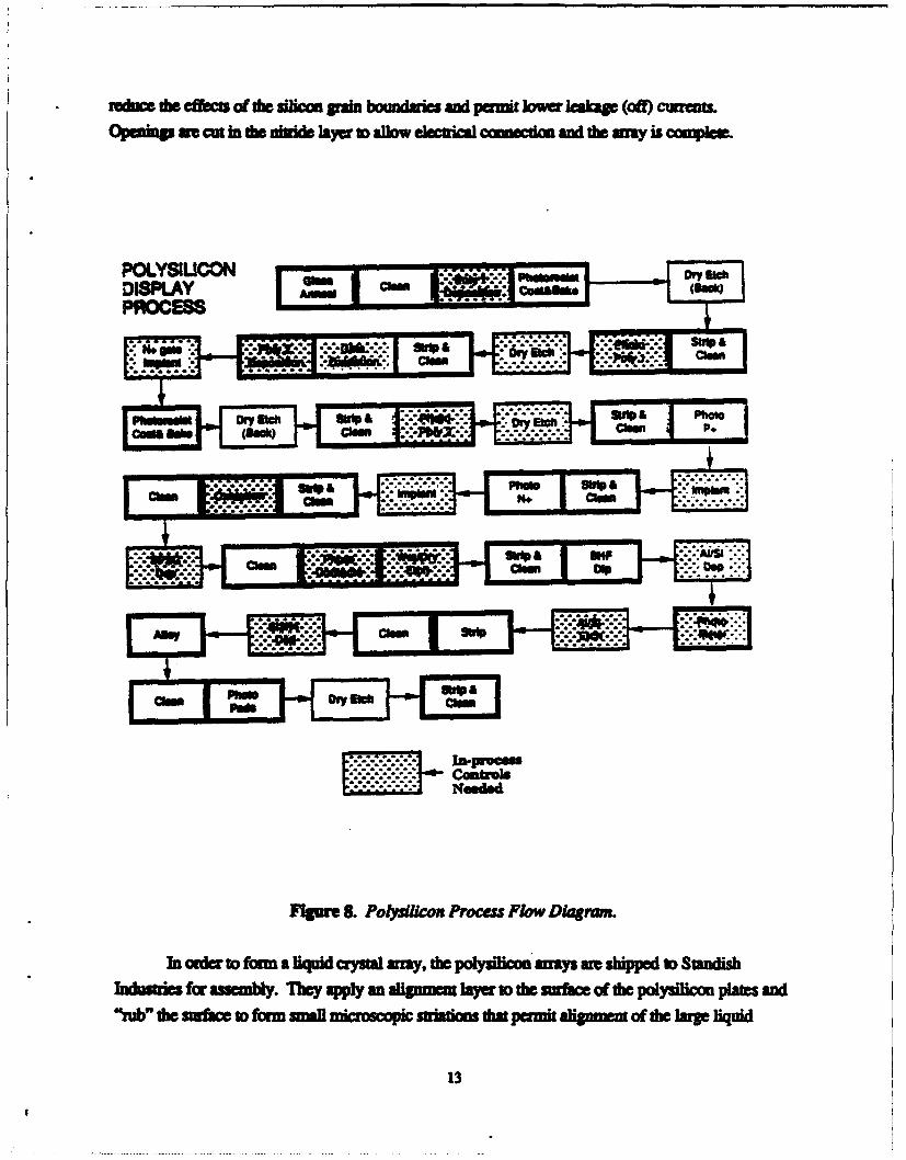
zedfnrp die ONOw d dtiesMc Fab botmduiwsandpautmizlwrla&kag (aft) cuummOpenins am cmr in fte nivd layar ao allw electica ocmieccu and t&e MY is OqlePeM
KXSUO *:-: so-
halo (Bodo
DISPLAYAw ~ i Cb muu soPROCESSeI I
JlgunP 8. &oyiio rca lwDar
Inorertofom lqidcrstl rmwi &oylio Drrys arohppdk SadsIn~~~kratriescw fo ase.y..e.p.ya..g.ir ayrs i sraeofdepiylio pae n
"rub" dMe surac &o fo. .rI .irsoi .t a .ha p. mi a.g n o. .. he lma r liqi
csý c13
phI
crylal filaculs. A top plM is then a•ttched to the polyuilican ple and the region between the
Mo pima is Med with liquid crystal materaL Aftwr saling of de fill par, the liquid crystalasoembly is complete and the display is ready to light up!
4.2. FABRICATION AND TEST EQUIPMENT UPGRADES
In ft section, the equipment and process upgrades that have ben implemented since thstart c the LCD Prorm in order ID aiev the gV o of increamd yield and imrvedmnut ability a listed, and exp ct on yid d •fthese changes is provided. Amlyield results will be trmed in Section 4.
1. TFT Fabrication Equipment Upgrades
The major equipment upgrades impe Me during the course of this program am Hstdbelow~
(1) hmmaion ofspndeveloper
(2) lntallation of class 10 photoresist bke oven
(3) Imprvement of HEPAs ovr the silicon etcher
(4) Upgrading of cleanroom:
(a) Install 16 new HEPA filter assemblies
(b) ln areasea of 16 return air ducts
(c) Enlarged changing a•r
(5) Conversion of cleaning baths to 100 percent quatz for exposed areas.
2. TFr Fabrication Process Changes
The major equipment process changes implemeted since the start of this program ar listed
below
(1) Impl on of routine cleaning of the oxidation fmrace
(2) Implmntaionof routine SMS and SPV em etsto omitor Si and
SiO2 quality
(3) Utilization of full bunny suits
14
(4) Change in procedure to allow only one person in the photorom during
3. Test, Repair, and Aumbly UpgradesA new laer repair system was installed that allows us to laser repair defects in the same test
bed that is used to measure plates and locate defects. This has lead to an approximate thre-fold
reduction in time taken for laser repair. No major changes were i2- n * in the assembly of
LCDs.
4.3. POLYSILICON PROCESS YIELD CHARACTERISTICS
1. Yield ModelA model has been previously developed for predicting the yields of display plates. The
input to this model is an estimate. of the defect level achieved on display plates processed in our
LAP. Each of these plates includes tes structures for measuring opens (serpentine) and shorts(in digitae). Thesee structures ar located on the periphey of •te plate. Since this region
usually suffers from a higher level of defects than central locations, these devices provid a worst-ase estimate. Teststructeexistfor. active polyilicon, gaw polysilicon, and aluminum levels
The polysilicon design rules me 6-Irm lines and spaces, and the aluminum design rules ar 8-pro
lines and spaces. The structures comprise a linear distance of 3.2 m. In addition, a sting of
83,200 6-x 6 Im contacts, in series with the active polysilicon level, and another string in serieswith the gate polysilicon levels, are monitored.
For active-matrix arrays and integrated drivers, a linear yield model is appropriate, i.e., theprobability of finding a defect is proportional to the length of certain tical lines. This is tute for
both opens and shorts. Shorts will occur between parallel lines of length, 1, and spacing. d. Thelonger the line and the closer the spacing, the more likely the short will occur. TIis is in contrast to
some yield models for integrated circuit chil, where the probability of defects occurring is
propotonal to the area of the chip.I the probability of a defect occurring is proportional to the length, and this probability is
Do per unit length, then it is easy to show that the yield for a line of length L i:
Y = exp-(DoL) (1)
We obtain the value of Do experimentally fiom the test structures of length 14 which have
measured yield Yb i.e.,
15
-= exp-(DoY (2)
The same yield model can be adapted to predict yiewl for redwxnat wuctum Forexample, consider the case of redundant data lines, i.e., every data line is driven separately from
each side of the acray. It then takes two defects in one line to produce a line defect, since for one
defect, the line segment on either side of the defect will be driven by its own driver.
From Eq. (1), the probability of obtaining a single defect on a particular data line is:
Pd = I - exp-(DoLe) (3)
where Ld is the length of a single data line. This expression is actually the probability that a data
line has any number of defects, but will be almost equal to the single-defect probability for smallD014. Now the probability that a particular data line, which is known to have one defect, has a
second defect, is simply the product Pd2. This follows from the assumption of statistical
independence. Therefore, the yield for a redundant data line is:
Yd =[I - (1 - exp-(DoLd))] (4)
and the redundant yield for the entire array of Nd data lines is:
Yd=[1 - (I-exp•(DoLd))2]Nd (5)
If DoLd << 1, exp-(DoLd) - 1 - DoLd, and.
Yd = [I-(DoLd)J2] Nd _ 1-Nd*(DoLd)2 (6)
In order to calculate yield, the display plate is separated into several key areas including:
(1) General busing
(2) Data scanners, including central and side busing
(3) Select scanners, taking driver redundancy into account
(4) Select to data shorts
(5) Data line opens.
16
Linm md spaces with critical dimensions were identfied for the aluminum, active
polysllcon, and gate polysilicon levels, and their lengths and widths were meamsud. Non-design-rule uied wids are given a linear weighting when calculating di ef•ective length. For instwne,a 14-pm-wide aluninum line of I m in length woudd be treated as the equivalent of an &/14-x l-mn-long line, or 0.57 m in effective length.
2. Yield Data for TFT ProcessApplying the yield model to the yield data that we have bown continuously monitoring for
aluminum, atov polysilicoa, and gate polysilicon levels, enables us to measure the effect ofinlrovements in the process. The following graphs, which are ordered chronologically, illusuatou progress. All of the yield calculations are based on test snuctures measuring opens and shortsyields for a given level. No provision has been made in our model to account for inter-levelshorts. We believe such shorts are insignificant compared with shorts within levels.
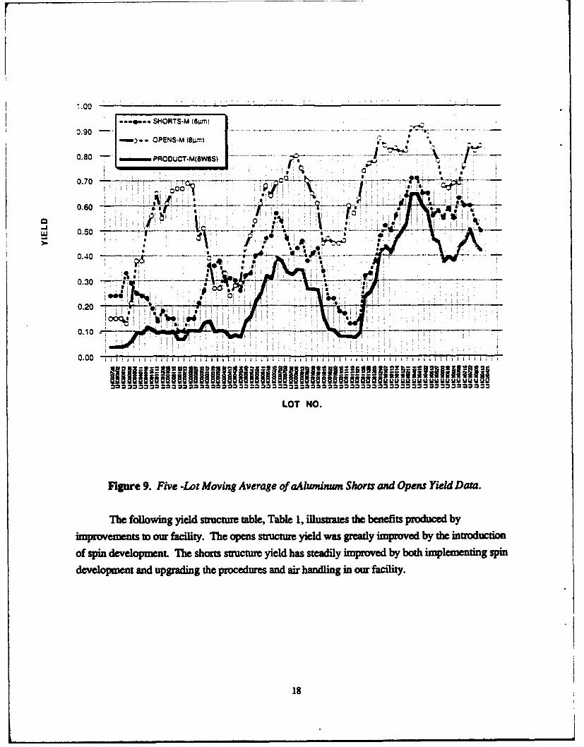
Figure 9 shows the aluminum-level yields for the opens mid shorts structures on actualTFT plates, averaged by lot, and plotted as a five-lot moving average, When there is a high levelof shorts, the opens structures ae less likely to fail, due to internal shorts in the serpentines, adwhen there is a high level of opens, due to aluminutm corrosion, for instance, the shorts strucambare less likely to fail, due to a high level of internal opens. T product of the two yields helpsbalance out these effects, and hence, is a more reliable number, or figure of merit. Figure 9 showsthat we have been successful at improving the aluminum yield; the figure of merit went from ahigh of 39 percent prior to 12190 to a high of 62 percent on these five-lot moving avepes.
Aluminum opens were improved by altering the etcing process to avoid over-etchig,hardening the photoresist, and rapidly removing the chlorine-laden resist after the etching prmces,by immersion in RT2, to arrest corrosion. Aluminum shorts were reduced by mounting the platesupside down during etching, paying careful attention to polymer build-up in the aluminum ewher,adding a spin developer, changing personnel procedures, and upgrading the air handling in ourfacility.
17
..00
-.@.. SI4ORTS.M (Um)i -
... .. ..... ..... .. .....-,.OPENS-M (8=-) I -
0.80 - - PROOUCT-M(8W6S) ................
0.60 -7 7j
LU .S 0.'o '
0.40 4
0.20
0.10
0.00 IiII 11 i III I I 111 I I I i
LOT NO.
Figure 9. Five -Lot Moving Average of aAlwninwn Shorts and Opens Yield Data.
T1he following yield structur table, Table 1, illustrates the benefits produced byimroeents, to our facility. The opens smtrutre yield was greatly improved by the introduction
of spin development. The shorts structur yield has steadily improved by both implementing sidevelopment and upgrading the procedures and air handling in our facility.
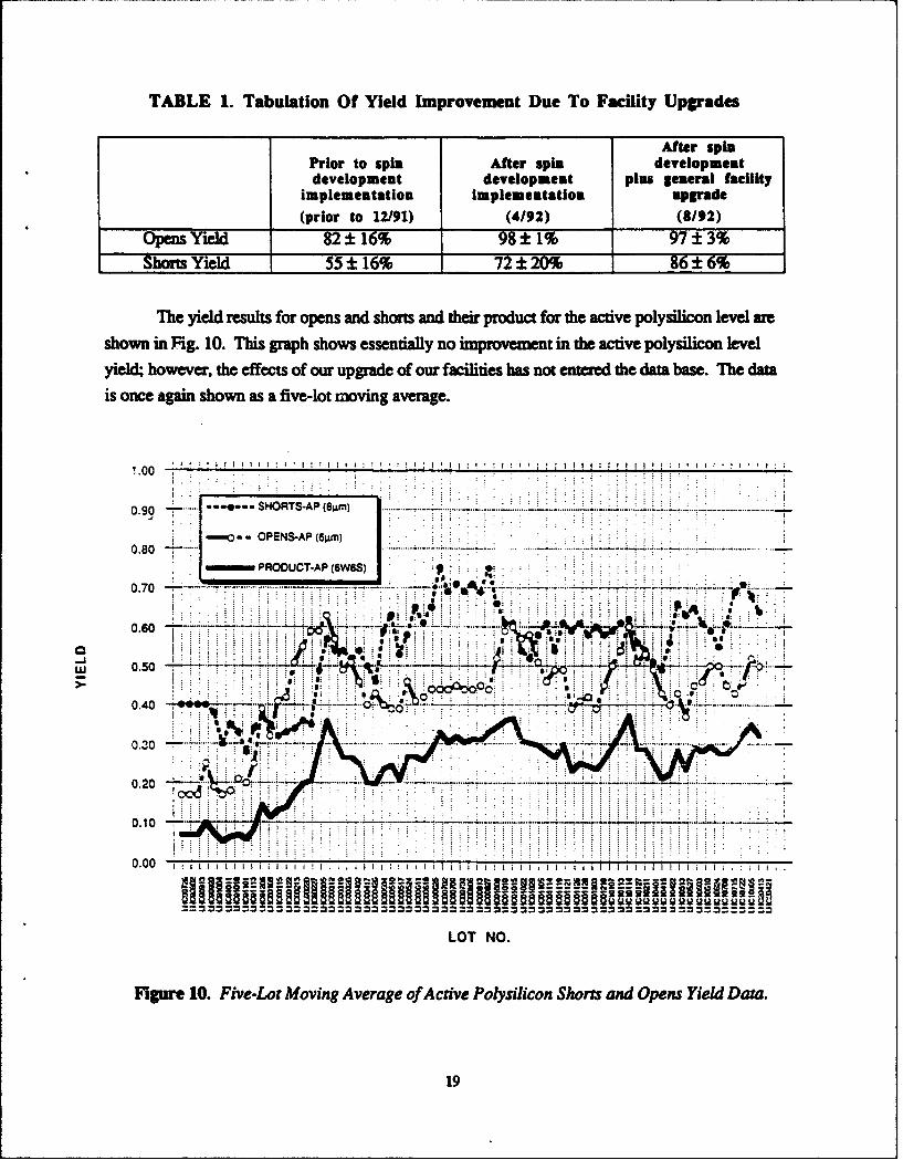
TABLE 1. Tabulation Of Yield Improvement Due To Facility Upgrades
After spinPrior to spin After spin developmentdevelopmen~t development plus general facility
implementation implementation upgrade_______________ (prior to 12/91) (4/92) (8/92)
Opens Yield 82±t16% 98±1% 97± 3%ShortsYield 55 ±16% _ 72 ±2W _ 86±6%
The yield results for opens and shorts and thei product for the active polysilicon level areshown in Fig. 10. This graph shows essentially no imp. emat in the active polysilicon Levelyield; however, the effects of our upgrade of our facilities has not entered the data base. The datais once again shown as a five-lot moving average.
1.00- IhII I-''.L 1.L 1 ?
0.0 -- c-s-SHORTS-AP (SIAM) ......
I .- OPENS-AP (6w±m)
- PRCOULCT-AP f6W6S)
d 80.60 - .U u.
wU 0.50 f7T..--- *
60.C0 - -
0.40 7 4, ...............I I II . I I i I I II I
L77NO
Figure 10. Five-L~~OtN oigAeaeo.ctv oyiio hrs n pn il aa
0. 0 i~i ..... .................. .. ... .. ....19..
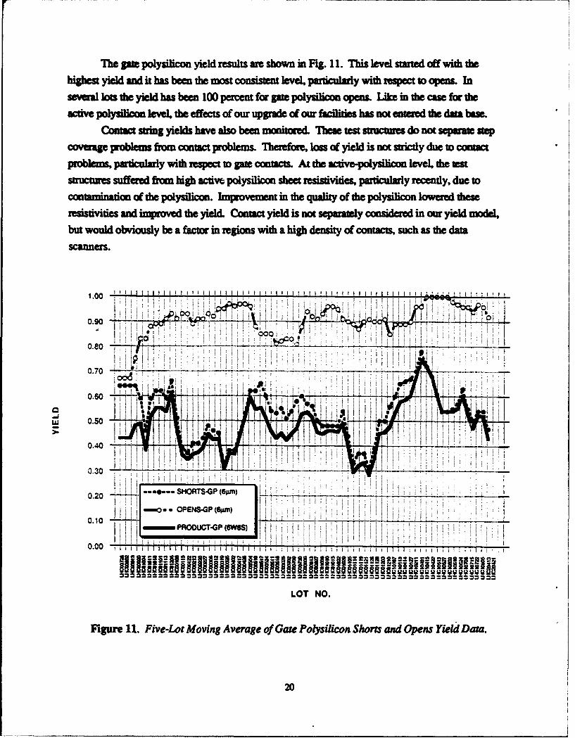
The gate polysilicon yield results art shown in Fig. 11. This level started off with thehighest yield and it has been the most consisten level, particularly with respect to opens. Inseveral lots the yield has been 100 percent for gate polyuilicon opens. Like in the case for theactive polyuilicoti level, the effects of our upgrade of our facilities, has not entered the data base.
Contact string yields have also been monitored. Thewe test structures do not separate stepcoverage problems from contact problems. Therefore loss of yield is not strictly due to contactproblems, particularly with respect to, gate contacts. At the active-polysilicon level, the teststrctre suffered from high activt polysilicon sheet resisnivities particularly recently, due tocon r-min-ation of the polysilicon. Imrv -n in the quality of the polysilicon lowered theseresistivities and imoproved the yield. Contact yield is not separately considered in our yield modelbut would obviously be a factor in regions with a high density of contacts, such as the datascanners.
1.00
0.90 - -C7X V
0.80
0.20 ~ RSG(p )
1:; .. OPE54(6n)
LU0.10 .. .......
I~ .. PHROUTS-GP (6WS0.2 WI
0.0 itgaaaa~a~a~aaaaa1'i'iaaElNaia-a:,a
0.10 PROnUnTnW 22W.8 88 8 . .. ... . . . .. ..
LOT NO.
Figure 11. Five-Lot Moving Average of Game Polysilicon Shorts and Opens Ykied Data
20
In making yield estimates based on ten structue yields, for lots s ed prior to December1, 1990, we chose the lot with the best product of opens and shorts yields, averaged over a single
lot, for that pticular level (see Table 2). This estimate shows our status at the start of the LC)
aProgram. A second estimate of yields is calclated using the best dam to date(11/15/92). These data were derived from special test plates upon which only one level was
patterned. To calculate the effective yield length, L, the display plate has been bromen down intovarious locatims: data lines in the army, select scanners, data scanners, general busing& select-to-
data short, pixel-to-pixel short, and pixel source-drain opens. Because there was 100 percentyield of the test structres for gate polysilicon opens in the lots selected, the critical area of the gate
lines was not calculated. Furthermore, the yield of the select lines is assumed to be 100 percent
The following lots were selected for the December 1, 1990 estimate, comparing yields for devices
similar in size to those on our test plates
TABLE 2. December 1990 Test Structure Yield
Opens Yield Shorts Yield
LHCO1 128 for the 83% 83%aluminum levelLHCO0305 for the active 67% 75%polysilcon level_ _ _ __ _ _ _ _
LHCO004 for the gate 100% 83%olysilicon level 100 _ 83%
Our best ee yield data on test patterns achieved yoe= 100 percent, yshm =94 percent
for aluminum test patterns (plate TSA20904-7 1), yopen = 99 percent, ydxot = 92 percent for active
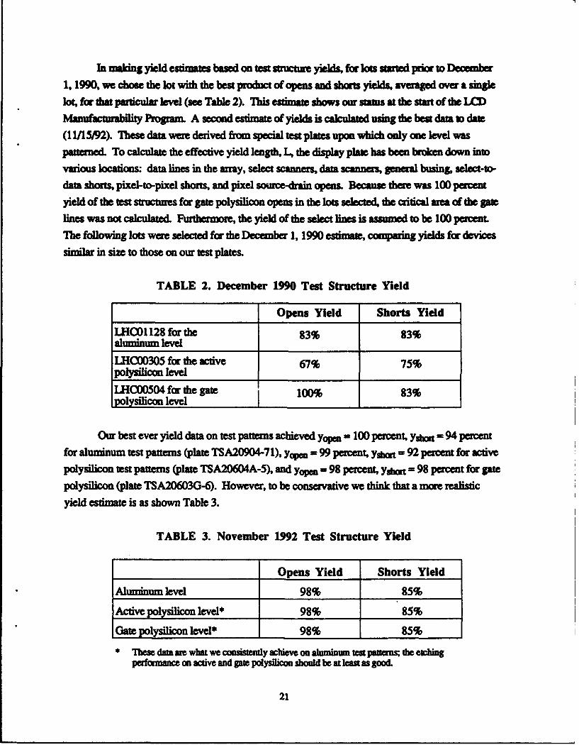
polysilicon test patterns (plate TSA20604A-5), and yope = 98 percent, ysbw = 98 paerent for gatepolysilicon (plate TSA20603G-6). However, to be conservative we think that a more realistic
yield estimate is as shown Table 3.
TABLE 3. November 1992 Test Structure Yield
Opens Yield Shorts Yield
Aluminum level 98% 85%
Active polysilicon level* 98% 85%
Gate polysilicon level* 98% 85%
* These daa are what we cmistmly achieve on awninuin test patens; dte eachingperformance on active and gate polysilicon should be at least as good.
21
4.4. YIELD ESTIMATES FOR LAF TFT PLATE FABRICATION
1. Model for Simple Active Matrix ArrayBy far the most troublesome yield problem for an AM TFr plate is that of open data lines.
The yield model in Section 4.3.2 above is used to correlate the data line yield to the test sctueyield and the result is plotted above. Note that to achie interesting yields (above 10 percent) the
test strcture yield must exceed 91 percent. Based on aluminum etching yields alone, the predicteddata line yields for plates processed in 1990 and those processed in 1992 ae shown in Table 4
below.
TABLE 4. Measured Yield of Test Structure and Calculated Yieldof Data Line Defect Free Displays at the Beginningand End of this Program
Measured aluminum test Calculated data lMe
structure opens yields defect-free MTF plate yield
1990 83% 1%
1992 98% 60%
Thus, we can see what dramatic progress has been made during the course of this program.
2. Model of AM Plate Including Integral ScannersWe now proceed with a more complete set of yield calculations for the case of an AM plate
that includes integral scanners. In constructing the yield model, we have assumed that defects arerandom and not caused by improper processing, systematic problems, or mishandling. For the
calculations that follow, we have made the following assumptions:
a. Input BusingInput buses are wide enough that opens are negligible.The yield loss due to shorts can be estimated from the aluminum test stucture yield and the
critical area, the gaps between the busing.Shorts between adjacent buses can be repaired 90 percent of the time.
b. Data ScannersWe estimate the yield of data scanners by assuming that the area of the scanner is occupied
by active poly, gate polysilicon, and aluminum in approximately equal amounts, that both shorts
22
and open contribute to the yield loss for each, and that the snt and open yields can be calculatedfiam the a structue yield.
N a daft scn is inoperable, we assume that we can substitue the data from a wmokingdata scanner aut the data line originally connected to an inoperable data sca .
When it is required, such a neare-neighbor repair is asumed to be somcsul 80 percentOfthe time.
c. Select ScannersThe yield is simlarly based on the test structure yield of active polyslli, gat
polysilicon and aluminum.Only one scanner is required to work all the way to the end so that an inoperable scanner
can be cut free 100% percent of the time.
d. Data LinesThe dominant soue of -onrepairable yield loss from our original display plate design
came ftom open data lines in the array. As mentioned above, we now can achieve opens yields onaluminum test structr in excess of 98 percent, which translates to data line yields exceeding 60percent and we would expect this to rise substantially as we move forward.
Although we could do a weld of one data line to its brlol neighbor to provide a signal tothe di ected bottom portion of this data line, we do not presently test the display for open datalines and, thus, do not do this repair.
Thus, our model does not assume data line repair.Yield predictions have been made using the above asumptions with the data collected from
the test structures providing the estimates of defect densities for each of the levels. For calculationsof the yield of the circuitry, we have used a somewhat more sophisticated model than thatdescribed above. The calculatioý , which are believed to be mem accurate over a specific limitedrange of yields, are based on the Murphy yield model (for y > 30 percent) and the Seed model (fory < 30 perent).
* ' pt below the results of these culatiMons assuming either (1) no nearest neighborsubstitution of data scanners or (2) nearest neighbor substitution of data scanners, which again issuccessful 80 percent of the time. In any case, we still assume repair of input busing (90 percenteffective), select scanner substitution (100 percent effective), and crossover shorts (also 100percent effective). This last assumption is only strictly true if either both select scanners areoperable or the short can be cleared without cutting a select line. This assumption does not appearto introduce significant error for the level of crossover shorts currently observed.
23
For the calculations of factory yield we mume dith the defect level is proportional to the
"class" of the facility. The measured airborne particulate level in our present pho-igfacility is typically 50 defects greater than 5 microns in a cubic foot of air. This is 5 times higher
than a class 10 facility. Thus, in our factory yield calculations, we have assumed defect densities
for all levels that are five times lower than our present (1992) test strcture measurements. See
Table 5.
The reason these two cases are of inmterest, is that in the fim case each pixel gets exactly
correct data, whereas in the second column, the data on one or me columns ae repeated to
achieve a"line defect free look."
TABLE 5. Calculated Repairable Yields of Data Line Defect FreeDisplays and of "Nearest Neighbor Data Scanner Substituted"Displays at the Beginning and End of this Program
TTFT plate yield without TFT plate yield a innearest neighbor data nearest neighbor datascanner substitution scanner substitution
1990 3% 14%
1992 7% 27%
Class 10 Factory 43% 59%
3. Model of AM Plate Incorporating Low TFr Count ScannersWe notice that for the existing design when fabicated in our present facility, the yield is
reduced from 60 to 27 percent by the incorporation of the present 5-blt data scanners and the
relatively complicated 20 TFT select scanners. Newer designs use considerably fewer TE7s. One
particular design incorporates as few as 20 TFrs in a data scanner (compared with the 120 per data
line in the existing design) and uses only 4 TFTs in the select scanner (compared with the present
20). Such a design would be significantly easier to faricate. The estimates, again assuming
nearest neighbor substitution or no substitution, are shown in Table 6.
TABLE 6. Calculated Repairable Yields of Data Line Defect FreeDisplays and of "Nearest Neighbor Data Scanner Substituted"Displays for Existing 5-Bit Design and for New Low TFTCount Design
TFT plate yield without TFT plate yield assumingnearest neighbor data nearest neighbor datascanner substitution scanner substitution
1992 14% 27%1992 (low TEE count designS 42% 57%
24
In this came the yield loss due to the priesece of scanwes is almot negligible.
4. Juss Related to Achieving a Une Defect Free TFT Plate fromn our LAF
a. Silicon Deposition, Etching, and Oxidation* Processes we under control.
b. Ion ImplantationProcess is under control.
c. DPSG Deposition and EtchingProcesses ine under control, although deposition is still somewhat dirty.
d. Aluminum Deposition and EtchingProcesses we under control.
e. Nitride DepositionThisprocss sep s currently dirty; the system is being upgraded to izprove cleanliness.
An alternative hydrogen passivation procedure needs derveiqunet for large ame to achieve evenIower leakage for small Pixes.
f. Black MatrixProcess is under control for etching the amorphous silicon. It is under developmentt for the
underlying nitride.
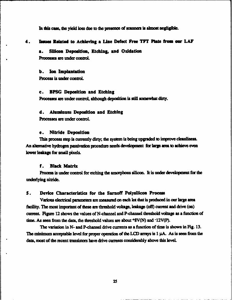
S. Device Characteristics for the Sarnoff Polysilicon ProcessVarious electrical parameters us measured on each lot that is produced in our large uam
faclity. T1e most important of thesweu threshold voltage, leakage (off) current and drive (on)current. Figure 12 shows the values of N-channel and P-channel threshold voltage as a function oftime. As seen from the data, the threshold values us about +8V(N) and -12V(P).
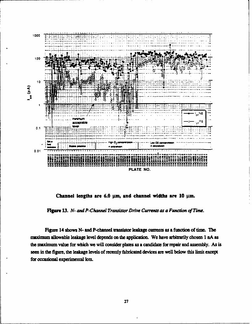
The variation in N- and P-channel drive currents as a function of time is shown in Fig. 13.The minmum acceptable level for prope operation of the LCD warys is 1 p&A As is senfrom the
* data, most of the recent transistors have drive currents cornsderably above this level.
25

AI
10 -
q! 17
.10 .1
-151
25I .....
-- -
PLATE NO.
Figur 12. N- and P-Channel Transistor Threshod Voltages as a Fuwndon of Time.
26
...................................... ....
;j7-
00
O~cofmi... ..... . . .
001 'N..
....... ........... U~ IijjS ~ Z ? ~ 4 ~
? .. ....... .. PLA TE. N .......... ..... . ...
Ch n e le..gths are.. 6. .and. .hn e ...dths are.. 10 .... ........... .
Fiue 3 - n PC ane rassorDiv ure.a a.. ... o .... f.. T ...e.
27M
100
10 -
~ I SW~ AX[ ~ ,o .... .....0.0 I I I I I I II I I I I ,.. I I I I
IIIIIIlidli ...iIU~i ... ....I ~ gaguawPLTRO
Channe .. lengths.. ar 6 .... an.han...th .re1
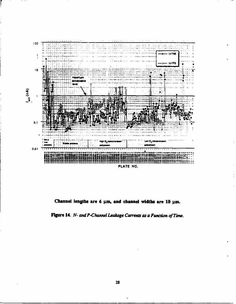
Fiue1.NTn -hne ekg weua ucino ie
287
5. DISPLAY SYSTEM
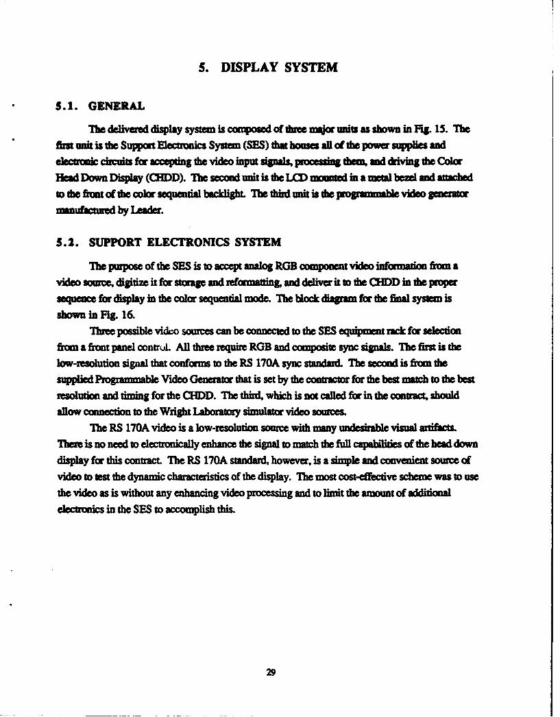
5 5.1. GENERAL
The delivered display system is composed of three mio unis as shown in Fig. 15. Thefirst unit is the Support Electronics System (SES) that houses all of the power supplies andelectronic circuits for accepting the video input signals, processing dm, and driving the ColorHead Down Display (QIDD). The second unit is the LCD mounted in a metal bezel and attachedID the front of the color sequential backlight. The third unit is the pormpnabe video gneratrn fa ed by Leader.
5.2. SUPPORT ELECTRONICS SYSTEM
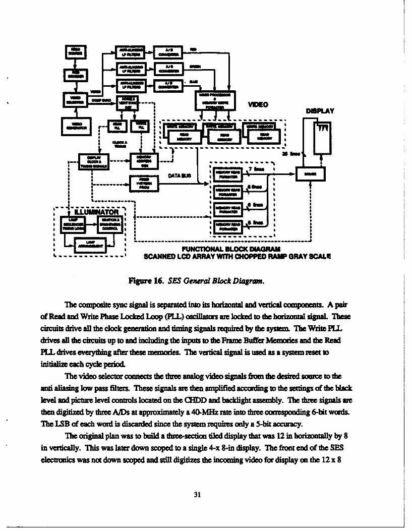
The purpose of the SES is to accept analog RGB component video information from avideo source, digitize it for storage and refo mattinL and deliver it to the CHDD in the propersequence for display in the color sequential mode. "The block diagram for the final system is
shown in Fig. 16."T=ree possible vido sources can be connected to the SES equipment rack for selection
from a front panel contrul All three require RGB and composite sync signals. The first is thelow-resolution signal that conforms to the RS 170A sync standard. The second is from thesupplid Ph, Video Generator that is set by the contracr for the best match to the besresolution and timing for the CIDD. The third, which is not called for in the contract, shouldallow connection to the Wright Laboratory simulator video sources.
The RS 170A video is a low-resolution source with many undesirable visual artifacts.There is no need to electronically enhance the signal to match the full capablifties of the head downdisplay for this contract The RS 170A standard, however, is a simple and convenient source ofvideo to test the dynamic characteristics of the display. The most cost-effective scheme was to usethe video as is without any enhancing video processing and to limit the amount of additionalelectronics in the SES to accomplish this.
29
urnr Mopk
E.5.3z
_ _ _ 2A
(30
r~a ... b...
L m -------
* mum meow--- -- --- --
I-5
- - - - - - -* * FUNCT~ItN 7LC DIGRm
F~n 6S wBbckAgrw
ch----i-sdrivePL eerthngaferthsemeores Te etia sinli
initializ--ycle --eriodconet the-- -- thewnlgvdosgasfo
anti~~L Ulaiglwps itr.Teesgnl r hnapiidaczigtlevel~~~~~----------- an0itr4ee otoslctdo i XD n akih seby h he inl r
the dgiizd y tre ADsatappoxmael a40mzrateitmhrecmepoan -btwr
The cmorigina planc wstobignld iseaathee-edo ie pahtws1 intis horizontall an etca opnemApn
dinvertially theircis wauaerdwpsoe to an inldngteinglstote Fram 8-in dipa.Temfont end ofthe Sead
eletronicsin lwpass noltes donhcoedwn stignll digties then apincoacoring vido for dsplayng on the 12lac8
leelan pctr lve cntol octe o teCHD ndbadih asebl Te heesin3s1r
forma This means that each horizontal line is sampled ly 1200 times, and all the
samples ae sent to the video write fonmatter. Tie first 400 and last 400 samples per horizontalline, are pas•ed to an open connctor and are lost. The center 400 sample -bizontal line are fed
through to the six frame buffers. These samp~les ame reformatted by stacking four con secutive 5-bitwords into a single 20-bit word for the SOS input data, bus.
The buffer meznry is composed of six separate frame buffers, two for each color. The
two frani buffers for each color are then operated in a mannw so tha while one is being written
into, the other is completely free to be read from. This ping-pong operation was selected for
maximumndependence between the Read and Write modes providing flexibility to -c 1da a900 image rotation if required. This memory structure also allowed a siple method of providing avideo freeze frame mode of operation that is helpful in image analysis.
The output video information from the frame buffers are reformatted in the four paralle-so-
serial reformatters for the high-speed clocking (8 MHz) to the CHDD. These reformaes int xthe data words and the five bits for each word for proper demultiplexing of the 4:1 demuliplexers
in the on-glass circuitry of the display.
The read clock is used to generate all the timing, control, and clock signals for the displayand the backlight controller. The data clocks, select clocks, gray-scale clocks, and data signals arelevel shifted by the driver circuit and fed to the display.
5.3. LIQUID CRYSTAL DISPLAY
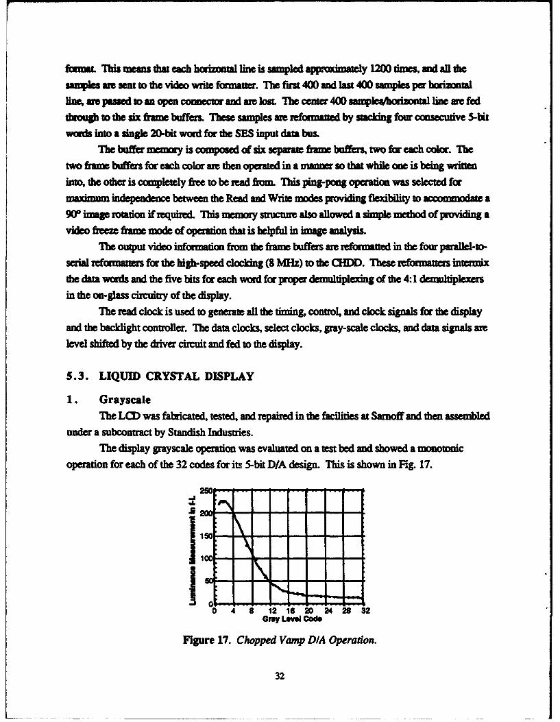
1. GrayscaleThe LO) was fabricated, tested, and repaired in the facilities at Sarnoff and then assembled
under a subcontact by Standish Industries.
The display grayscale operation was evaluated on a test bed and showed a monotonic
operation for each of the 32 codes for its 5-bit D/A design. This is shown in Fig. 17.
10 I.4 2S4 3
Gray L Code 28 2
Figure 17/. C.hopped Vamp DIA Operation.
32
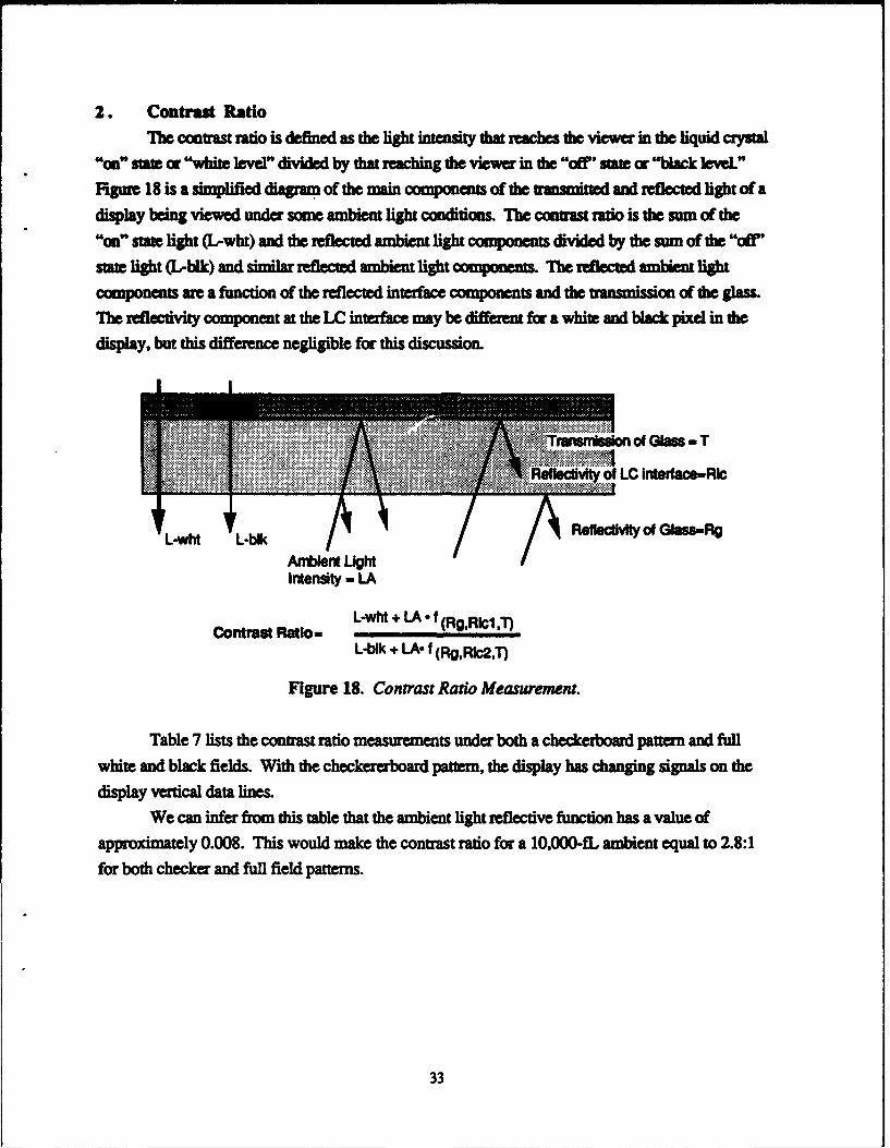
2. Contrast RatioThe contrast ratio is defined as the light intensity that reaches the viewer in the liquid crystal
"on state or "white level" divided by that reaching the viewer in the "off' s=t or "black leveL"
Figr 18 is a simplified diagram of the main components of the atnited and reflected light of a
display being viewed under some ambient light conditions. The contrast ratio is the sum of the
"on" state light (L-whO and the reflected ambient light components divided by the sum of the "off'
state light (L-blk) and similar reflected ambient light components. The reflected ambient lightcomponents are a function of the reflected interface components and the transmission of the glass.
The reflectvity component at the LC interface may be different for a white and black pixel in the
display, but this difference negligible for this discussion.
................ ....- X-1.~ Jf~I~lf~n
Reflectivity of IC interface-Ric
L-wAm -wht +b Aly of G(ass.,Rg
Intensity - LA
Contrast Ratio L-Wht + L f (Rg RId 1)
L-blk + LA f (RgRIc2,T)
Figure 18. Contrast Ratio Measurement.
Table 7 lists the contrast ratio measurements under both a checkerboard pattern and full
white and black fields. With the checkererboard pattern, the display has changing signals on the
display vertical data lines.
We can infer from this table that the ambient light reflective function has a value of
approximately 0.008. This would make the contrast ratio for a 10,000-fl ambient equal to 2.8:1
for both checker and full field patterns.
33
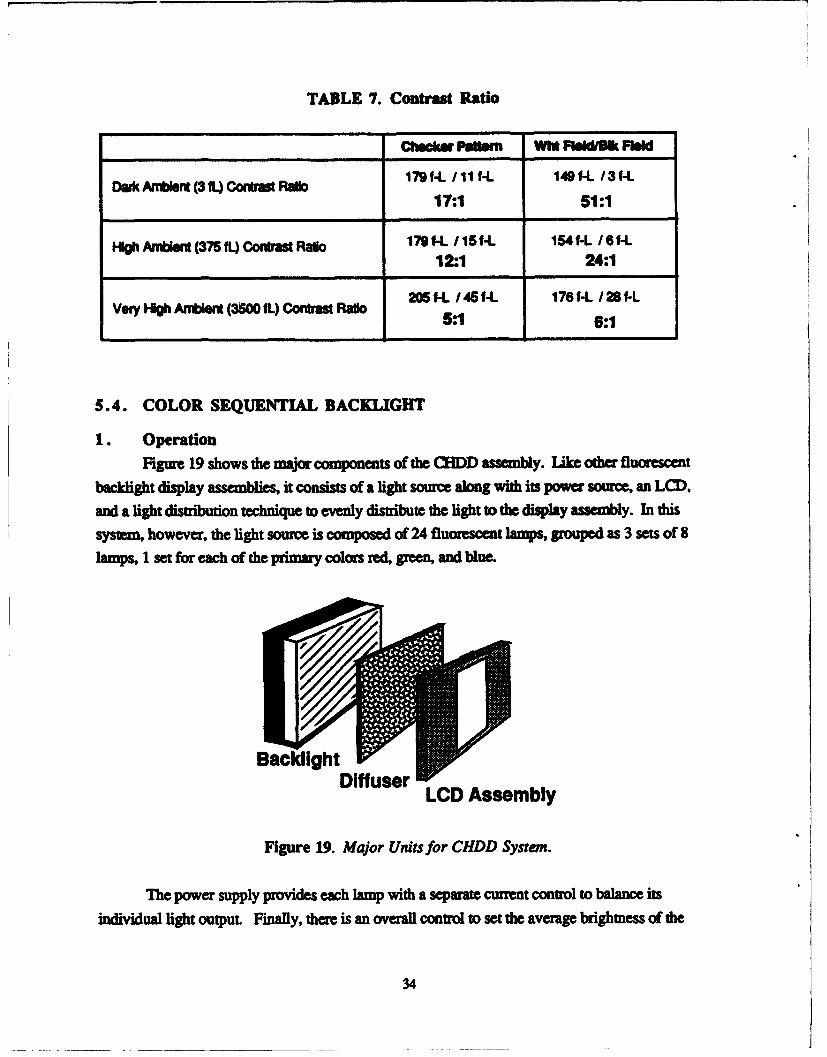
TABLE 7. Contrast Ratio
ChockSr Pattem WMt RO& O d
179f-L/ Ill f-L 149f-L/3f-LDWk Amlent~ (3 .) COMMai Ra~o17:1 51:1
HO M (375fL) Cor&W Rob 179f-L /SfL 154f-L /6f-L
12:1 24:1
205 f-L/45f-L 176K/ 28 -LVery H~h MU (3600 fL) CoW&Ma Rado5.1 6:1
5.4. COLOR SEQUENTIAL BACKLIGHT
I. Operation
Figure 19 shows the major components of the CHDD assembly. Like other fluores=ent
backlight display assemblies, it consists of a light source along with its power source, an LCD.and a light distribution technique to evenly distribute the light to the display assembly. In this
system, however, the light source is composed of 24 fluorescent lamps, grouped as 3 sets of 8lamps, 1 set for each of the primary colors red, green, and blue.
BacklightLCD Assembly
Figure 19. Major Units for CHDD Sysem.
The power supply provides each lamp with a separate current control to balance its
individual light output. Finally, there is an overall control to set the average brightness of the
34

display. Bach mp has a separat switec control in the pmw supply da is controlled by the kWcsefb c video drive electonics to the LCD. In this mmnum, te exact m-on poit andlent of on-tim for each lamp isexternally conrlle in relaton to the other displayseemng
The types of fluoresce lamps used ma reflec•or types purchased under a subconuc fromGTE. These lamps have Iwdntenlrflectiv coatings betee the bulb wall and the phosphorcoatig A narrow slit runs lengthwise along the bulb to create an exit poct for the •• t This eaipart has a phosphor coating in the reflectr bulb but is let clde for th asperto lamp. Thes lampsai slightly less efficient than normal fluorescent lamps due to their small diametrz and highcurrens but the narrow beam light output Iharctristic make them ideal for this application.
A simple diffuser was the original, technique planned to be used to distribute the lightevenly to the rear of the LCD assembly. It is recognized that some brightness and uniAmity ofthe display is lost, but the cost of the optics for this step verses the qualitative resul of thedisplayed pattern was of primary concern.
The opemon of the field-sequential color system is illusua in Fig. 20. For a typicalhorizontal Interlaced 30 ftmes/kc video source, six color fields an created. There is one odd andone even field for each primary color called Ro, Go, Bo, RE, Ge, and Be, as shown. These
signals are electrnically stred in the display electronics, reformatted, and oaded into the display.
01 R0 1 0 1201 MIE 1*1 E ]Lmw $"Pencem
hIHIIIIIIIIIII IG: :G : :r R R R R R R
G 0 G G G. R R R R R RG G0 0- & - . R R R R R R
G G 0 0 R:::: R R R R R0 0 G G G..- R R R R R R
0 G 0 G :::: R R R R R RG G 0 G Gaa.... R R R R R RI
Figure 20. Video and Backlight Sequencng.
35
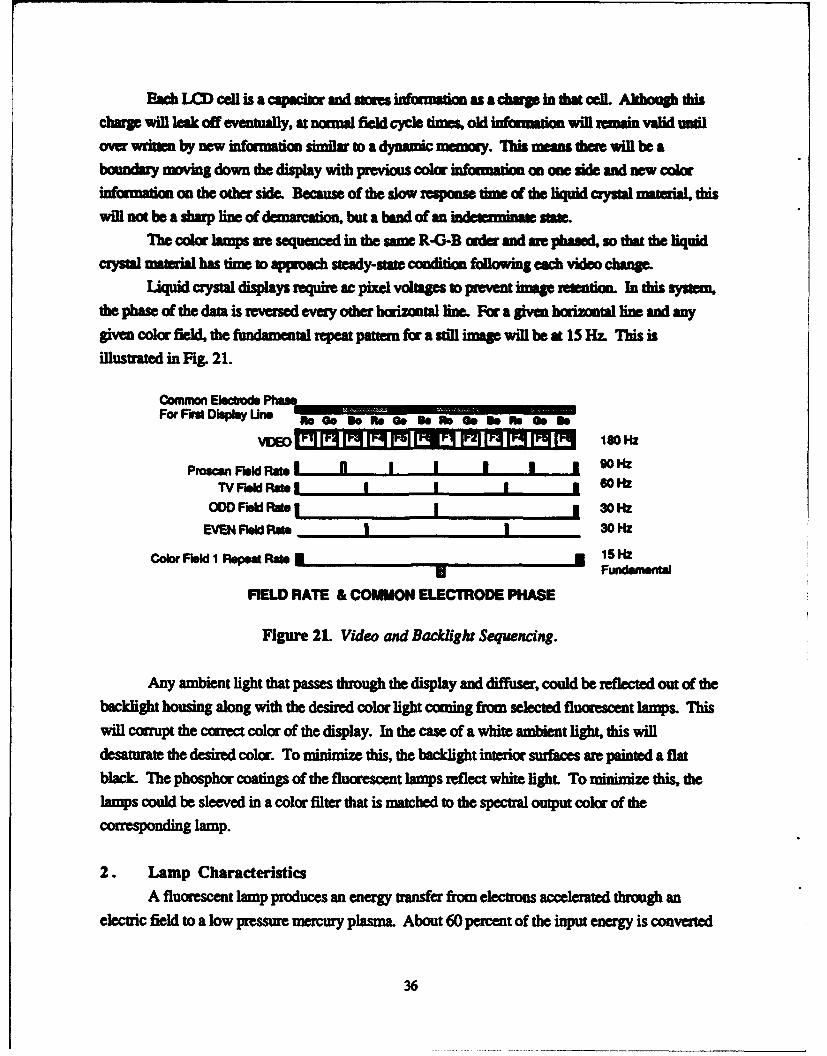
Each LJCD cell is a capaitor and store infwtomatn as a charg in that cell. Although dhischarge ill leak off eventually, at normnal field cycle times, old information will reawin valid untilover wmite by new information simila to a dynamic umeny. Thia means there will be aboundary moving down die display with previouis cokor informtinad on one side and new colorinformiation on the other side. Because of the slow response time of the liquid crystal materiakl, thiswill not be a sharp line of demarcation, but a band of an ndtrnaestatle.
Ile color lamps ate sequenced in the same R-G-B ordler andm peihased, so that the liquidcrystal material has time to appmoch steady-state condition following each video change.
Iliquid crystal displays require ac pixel voltages to preven image retention. In this systm,die phase of the data is reversed every other horizontal line. For a give horizontal line and anygiven color field the fundamental repeat pattern for a still imag will be at 15 Hz. Thiis, isillustrated in Fig. 21.
Comnmo Elactud a ri
For Firs Display Ln . .~..VI)EO qrMI Mpq Mr P qP 180 Hk
Proacan Field Rate I I -I[ I 1 1 90HNzTV Field Rd@ I 1 60HIz
OODDFieW de~. 30H1-z
EVEN Field Ri. 30 Hz
Color Field I Repeat RWA 0 .5HZFundamwental
FIELD RATE & COMMON ELECTRODE PHASE
Figure 21. Video and Backlight Sequncing.
Any ambient light that passes through the display and diffuse, could be reflected out of thebacklight housing along with the desired color light coming from sdelcte fluorescent lampsL Tibswill corrpt the correct color of the display. In the case of a white ambient light, thiis willdesaturate the desied color. To minimize this, the backlight interior surfaces are painited a flatblack The phosphor coatings of the fluorescent lamps reflect white light. To minimitze this, thelamps could be sleeved in a color filter that is matched to the spectral output color of thecorresponding lamp.
2. Lamp CharacteristicsA fluorescent lamp produces an energy transfer fr-om, electrons accelerated through an
electric field to a low pressur mercury plasma. About 60 percent of the input energy is converted
36

to the mission of UV light at a wavelength of 2537 A. Thw inner surface of the lamp is conedwith phosphns selected to transform the 2537-A light down to the desired cor . A givenphospc •can only absorb and convmr to useful visible ligh p al mognetic radiation within a
specific wavelength ane at an efficency of about 45 percent. In a•don there is a bulb andphosphor absorption loss of about 15 percent.7 Couple these effi=n with the averageluminou efficiency for a white fluorescent light of about 57 percent and the resoltant nxin
luminous efficiency of 680 lumensiW for 5550-A light is reduced to about 88 lumens/W. The
small dimeter, short length apere and reflecr style lamps are less efficien than ths and arerated at 60 lumens/W in a continuously operating mode.8
li process that produces the iniial electrons is important to the lamp efficiency and life.There are two types of electron mission used in present com ial ac lamp operation, thermionicemission or hot cathode and cold cathode. The hot cathode has a life Of 5000 to 15000hours while the cold cathode has a life of 10,000 to 20,000 hours. lTw hot cathode has a "cathode
fall" potential, which is part of the cathode loss factoms, of 12-15 V while di value for do ed
cathode is 120-150 V. Although the cold cathode lamps are known for their long life, ability to
tolert high peak currnts short duty cycles, and have a large dimming range 9 they are not
desirable in this application. This is because of a long unlit area at the ends of the tubes and the
higher starting voltage required to strfk the plasma.lOThe color-sequential system requires a pulse-type mode of operation that also inf the
need for a hot cathode because of th operating speeds needed. This continuous heate power will
decrease th efficiency value. A heater element is required at each end of the lamp for bidirectional
current flow to prevent mercury migration within the lamp. Some form of alternate end heating
and operation is required to minimize this energy loss. These heaters consume 1 W each.
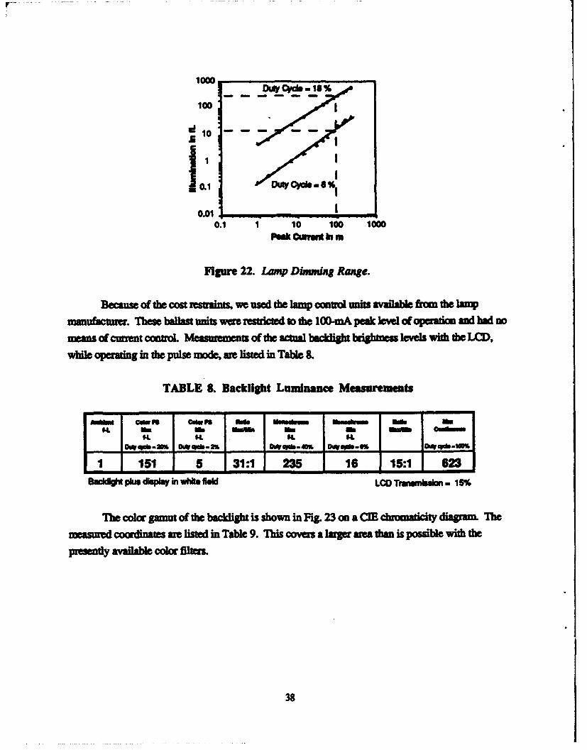
Dimming of fluorescent light sources can be accomplished either by controlling the currentto the lamp or by conutolling the duty cycle of the drive signal when the limp is operating in a pulse
mode.Varying a lamp current from 1 to 100 mA should give a dimming range of just under
1000:1 as shown in Fig. 22. The data for this figure were taken from a yellow-green fluorescent
lamp and show that the additional dimming range for a 4000:1 ratio can be obtdned by controlling
the duty cycle of the lamp.
37
1000DLObCydm IS %
100
W 10 - ---
10.1 ,"Duty Cycb - 0
0.01
0.1 1 10 100 1000I:• Cumimt In m
Figum 22. Lamp Dming Range.
Because of the cost restrints, we~ used the lam conWo units availbl fiun the lamp9aufcurr Tieme ballas units were restricted to the 100-mA peak leve of operation and bad no
means of current cotoL Measuemens of the actual bckligh r levels with the LCD,while operating in the pulse mode, ie listed in Table 8.
TABLE 8. Backlight Luminance Measurements
Amam---- CdWM'P COIZPO IMel kbts fimlshs agoi am,
m.u -t t11. -i.-
w.%DW*P-2% OWWOdm% O O~qdsf11 151 31:1 235 16 15:1 623
B=Ckt p- display in whie ed LCD TruuAmion - 15%
The color gmut of the badcklight is shown in Fig. 23 on a CE chrmaticity diaga Mhmeasured coodlinates are listed in Table 9. T"his covers a large area than is possible with thepresently availabl color lters.
38

rr 510
11
S-•-la-
6-
0.. 6-
I I76 __
y 0 - - - - - h ----
-4 - -40000 -
--- ,-nmnm0.u 000
490
0x 14 0.
0. d. 2 3 4 -A-7 -7- .
y 0.3397 0.6475 0.1114 0.3171
u 0.4096 0.1006 0.1546 0.1865
v_ 0.5206 0.5683 0.2491 0.4585
39
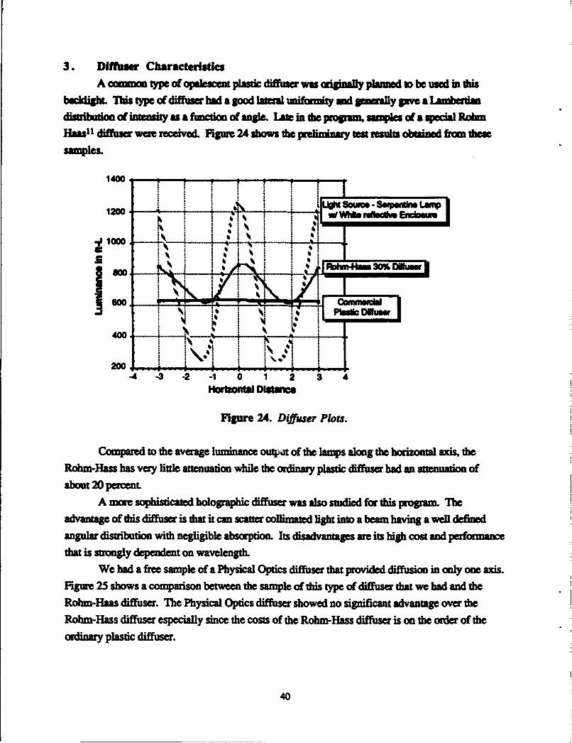
3. Diffuwr CharacteristicsA common type of opalescent plastic diffuser was originally plnwd I be used in dtis
backlight. This type of diffuser had a good latal unifoniy and emi ally pave a Landerdandistributon of intesity as a function of angle. Lat in die program. mvple of a special Rum.Hu 1 diuser we received. Figure 24 shows di prelinnary test results, obained fm theseSamiples.
1400- W ?emdWEw
h II
400 i. - -
- 2iKI
20 ... ,j1 w\.. ,'ww .L_.w _I-4 -3 -2 -1 0 1 2 3 4
HoFn Dnstanc
Figure 24. D(ffuer Plots.
Compare to the average lumnanmce outpat of the lamps along the horizontal axs theRohim-Hass has very little atteuation while the ordinazy plastic diffuser had an attenuation ofabout 20 percent.
A more sophisticated holographic diffuser was also studied for thi program. Theadvantage of thlis difue is that it can ii scte ollimated light into a bea having awell defindangutlar distribution with negligible absorption. Its disadvantages are its high cost and performancethat is strongly dependent on wavelength.
We had a free sample of a Physical Optics diffuser tha provided diffusion in only one axis.Figure 25 shows a comparison between the sample of this type of diffuser that we had and theRohm-Haas diffuser. The Physical Optics diffuser showed no significant advantage over theRohm-Hass diffuser especially since the costs of the Rohm-Hass difue is on the order ofthordinary plastic diffuser.
40
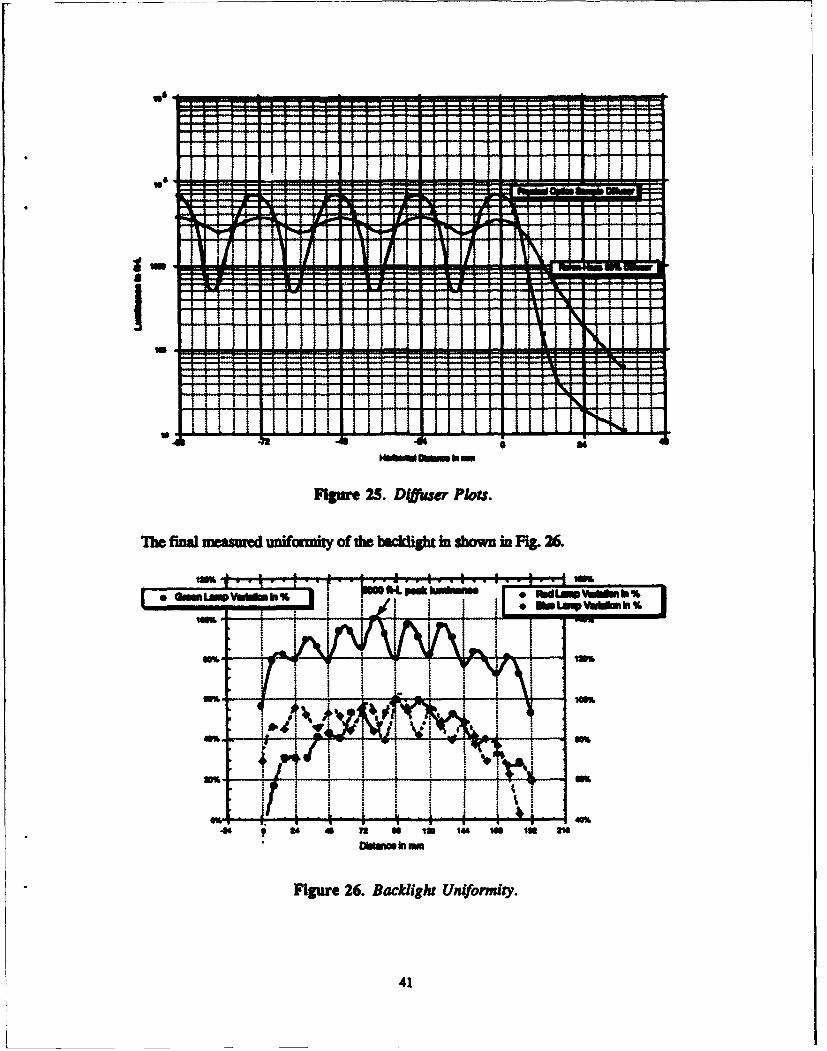
'IIN
Figure 25. D(7uer Plots.
11c final mansued unifonnity of the backlgh: in show in Fig. 26.
Gam~mp~akf In huimn * ft~w d1M%
if * im~lnI
Figure 26. Backlight Uniformity.
41
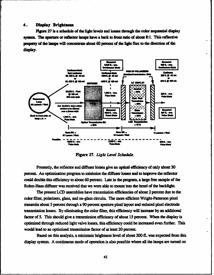
4. Display BriglhtmmFigiuse 27 is a schedulet of the light lewhl and loomi tough the coloe sequential display
sysem Mwe spusie or reflector lamps bane a back to ftirost to, of about 8:1. T1his relectivepropety of the lamps will concmawate about 6D perent of the light flux to the direction of tdo
display.
AMOVML* 0" ML O 49OLMLOWMmw-b ___~w O81A X&"
3 3W~dVP
Nub
4.AL0 Zc.'
011
amue27 i~ MLevel Scheule
Presently, the refleco and difuser losses give an optical efficiency of only about 30percent. An optimiza~tion progra to mianimz the diffuiser losses and to improve fth reflectorcould. double thi efficiency to about 60 percent. Lae in the program, a larg free sample of theRonim-Hass diffuser was received that we were able to mount into the bead of the backhght
The present LCD assemblies have transmission efficiencies of about 2 percent due to thecolor filter, polarizers, glass, and on-glass circuits. The manc efficient Wright-Patterso pixel.transmits about 3 percent through a 90 percent aperture pixel layout and reduced pixel electrode
trnsission losses. By eliminating the color filter, this efficiecy will increase by an additionalfactor of 5. This should give a transmission efficiency of about 15 percient. When the display isoptimized through reduced light valve losses, this efficiency could be increased eve further. Thiswould lead to an optimized transmission factor of at least 20 percent.
Based on this analysis, a midnimumn brightness level of about 200 &L was expected from thisdisplay system. A continuous mode of operation is also possible where all the lamps are turned on
42
to pw~dUC a -rgh white Wig1U Theluinescence levels atc listed ai he figure mad show amaxmum pacica1 brighmneus level of 675 fL
Actual m - s alt sh own in Fig. 27 and show a lower luinanaie dha mzpectedfor she pulse mnode operation due to a snule duty cycle, but a larger hanminno leel in thecontinuous mode of OpzmioIL
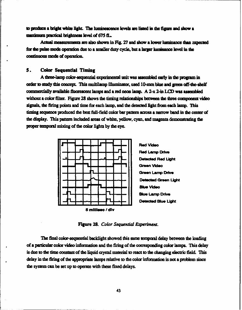
S. Color Sequential TimingA thre-lamp color-sequential expeimental unit was assembled early in the ppropm in
mrler to study this concept. Ibis mnulti]am llhaminator, used 10-mm. biue and green off-die-shelfcomPecially availa"l fluorescent lamps and a red neon lanmp. A 2-x 2-in LCD was assembledwithout a color filter. Figure 28 shows the tuming relationships between die thee component videsignals, the firing points and time for each lamp, and the detected light frnom each lamp. Thistiming sequence produced the best full-field color bar pattern sross a narsw band in the center ofthe display. This pattern included areas of white, yellow, cyan and magenta dmnttngtheproper temporal mixng of the color lights by die eye.
Red VideoPled Larnp Driv
ýA Detected Pled UghtGreen Video
net1cted Green UghtSkis Video
Detected Bue L1ht
5 minlleec dlv
Figure 28. Color Sequendl Experiment.
The final color-sequential backlight showed this same temporal delay between the loadingof a particular color video information and the firing of the corrwnesoding color lamps. This delayis due to the time cons=an of the liquid crystal material wo reac to the changing electric fielcL Thisdelay in the firing of the appropriate lamps relative to the color information is not a problemsicthe syste can be set up to operat with these fixed delays.
43
Sequencing throughi dham successive different color video fields minuls hi a low cowast:hanp When an LCD is sequenced though a series of identical video fields, the liquid cystalaligmnout can build to a final casyrec t steady state and overcome the time constant delay. DisioniolnIo the lquid. crystal cell voltage due to the ch dielectric constant of the liquid cryal materialas Its alignment changes is also overcome with the repeating field information. The sqecndiffint color fields does not allow for this integration to a ca contrast level, andinorccolor light will lek thogh the display a cause a desattion of the desited color.
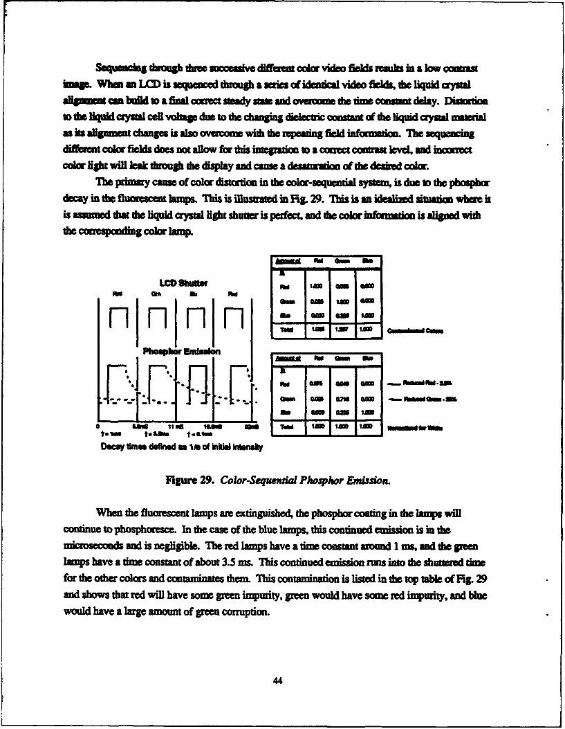
The primary caus of color diation in the color-sequential, systm is due to th phosphordecay in the fluorescent lamps. Ths is illustrated in MS.~ 29. Ti~s is an idealized situation. where itis assumed that the liquid crystal light shutter is p•rfect, and the color informato is aligned withthe c( nding color lamp.
ANN" - -
LCD Mhutter -- m
m1 nr nn
n n n n - -W I-
Phosphor Em29uon Ag o "
a* m ama Im= ~ u~i
a j WMG am UNe ~trnuntrtau" tSa3.t teeiaaftw-*
D"cay 15m defined as lie of imkWa Wft~nivf
Figur 29. Color-Sequen"a Phosphor Emwssion.
When the fluorescent lamps are cxtinguished, the phosphor coating in the lamps willcontinue to ph. In the case of the blue lamps, this continued emission is in themio and is negligible. The red lamps have a time constant around 1 ms, and the greenlamps have a time constant of about 3.5 ins. This continued emission runs into the shumered timefor the other colors and contaminates them. TIis containation is listed in dt top table of Rig 29and shows that red will have some green impurity, green would have some red impuity, and blue
would have a large amount of green comrrption.
44
If the th sets of color lamps whenr adjusted and normalzed for the bes whi, the colodisplay would have the reds rduvud by 2.5 pecent and the gem by 28 perMent. This would give
the dsly the best black and white images but the color images would tend t look bluish
45
6. SILICON TRANSFER PROGRAM SUMMARY
Functional single-crystal silicon 192 x 192 transmissive ANM have been denstrated,
The 2.5-x 2.5-in display with integrated scan and drive functions was fabricated in a thin-film x-Si
silicon-on-insulator (SOI) wafer using standard IC processing and subsequently transferred to
glass. Comparison of device characteristics pre- and posttrander shows that no degradation of
device performance or introduction of defects is associated with this process. Measmued devicechrateisics such as leakage current, transconductance, and speed are as expected for single-
crystal silicon. Twisted nematic AMLCDs were assembled with this circuit using conventional
techniques. This work focused on the use of x-Si because of the advantages discussed.
However, the same technique could be used to fabricate displays using amorphous or poly-Si.
Thin fiams of x-Si formed by other techniques, such as oxygen implantation (SIMOX) or wafer
bonding, could also be used for AMLCD fabrication. The 192 x 192 AMLCDs fabricated with
transfer silicon show excellent contrast ratio and picurn quality. The speed, low leakage current,
and high drive capability of single-crystal silicon devices should allow the fabrication of displays
with integrated system-level peripheral circuitry, high pixel density, and improved contrast and
optical aperture ratios.
6.1. INTRODUCTION
The conventional approach to AMLC:s relies on the fabrication of circuitry in thin layers
of amorphous or polycrystalline silicon deposited on glass or quartz substrates. These substrates
provide the optical transparency necessary for transmissive displays but the quality of the deposited
silicon films limits ciruit performance. The speed, low-leakage current, and high-drive capability
of single-crystal silicon (x-Si) devices should allow the fabrication of high density displays with
improved conrast and optical aperture ratios and integrated system-level peripheral circuitry.
However, no technique has yet been developed to attain single-crystal quality silicon directly
deposited in thin-film form on glass or quartz substrates.
Under this program, an approach for the fabrication of transmissive AMLCDs that allows
circuitry to first be fabricated in thin-film x-Si, using standard IC processing, and subsequently
placed on glass has been demonstrated. A functional monochrome 192 x 192 AMLCD with
integrated drive and scan circuitry has been fabricated using this technique. While a transfer
technique has been used to prepare a poly-Si display on glass,' 2 this work dem the first
transmissive AMLCD formed from x-Si.
46
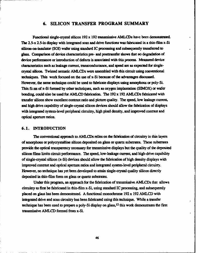
6.2. THIN-FILM x-Si MATERIALS
The starting material for circuit processing was thin-film x-Si prepared by the IsolatedSilicon Epitaxy (ISEun) process.1 3 In this process a thin film of x-Si is formed on an oxidized Si
wafer (silicon-on-insulator material). As illustrated in Fig. 30, an oxide layer is formed on thesurface of a standard single-crystal silicon wafer except for a small area near the edge of the wafer.
The wafer is then coated with vapor deposited poly-Si and encapsulated with an oxide cap layer.
The wafer is then uniformly heated to a bias temperature and scanned with a hot filament to
directionally recrystallize the poly-Si layer using the original Si wafer as a seed to form a thin x-Si
film on the buried oxide. The x-Si layer formed in this fashion has electronic properties
comparable to a silicon wafer used for standard IC fabrication. 14
Isolated Silicon Epitaxv
Strip HeaterSingle Crystal Si
Polvsilicon --o-- meltOxide
Figure 30. Silicon-on-Insulator Materials Fabrication Process.
47

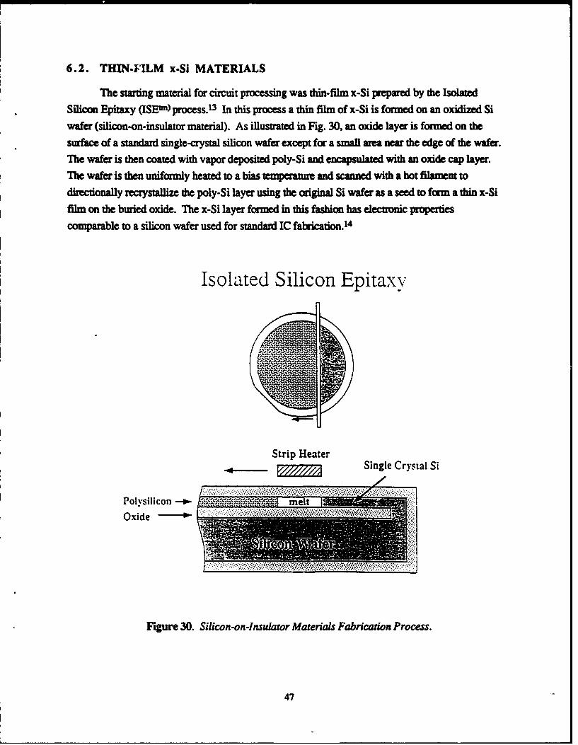
After removal of the cap layer, cucuiuy can be formed in the thin x-Si layer using standaidintegnied circuit (IC) processes and equipmenL The properties of the buried oxide layer can be
used to facilia removal of the x-Si layer, containing tw integrated circuit, from the ouiginal Siwater substrt.
6.3. DISPLAY FABRICATION
The display circuit used for this demonstration contained a 192 x 192 pixel active matrixwith integrated drive and scan functions. This circuit design and layout had been developed for apolycrystalline silicon display.15 The circuit processing sequence is illustrated in Fig. 31. Thethin-film x-Si layer of the 4-in-diameter starting wafer was 0.3 pm thick on a 1-jim-thick buriedoxide layer. The x-Si film was patterned using a dry etch technique to form Si islands that werethermally oxidized to form a 70-nm-thick gate oxide. Boron and phosphorus were implanted intothe Si islands for threshold voltage control of the n- and p-channel MOS transistors. A layer ofLPCVD polysilicon was then deposited at 5600C to a thickness of 0.5 pm and patterned to form thtransistor gates. Phosphorous and boron implants were used to dope the source/drain regions andan APCVD Boron-Phosphorus-Silicon-Glass (BPSG) was deposited over the surface to form theinterlayer dielectric. The wafers were then heated to 850*C for 20 minutes to flow the BPSG andactivate the implants, contact vias were opened in the glass and reflowed, and aluminum metal wasdeposited and defined to form the interconnect patte•. A silicon nitride layer was deposited overthe surface of the wafers prior to 4500C contact sintering. After army processing the wafers, someof the earlier wafers were neutron irradiated in order to minimize effects associated with the highcarrier lifetime in the x-Si film. After a circuit redesign to add substrate ties, the neuuro irradiationwas eliminated from the process.
A unique feature of this display is that the pixel electrodes are formed from implanted x-Si,not poly-Si or ITO, resulting in a simplified process scheme. The x-Si layer has approximatelyfour times the optical transparency of poly-Si films of equivalent thickness.16
48
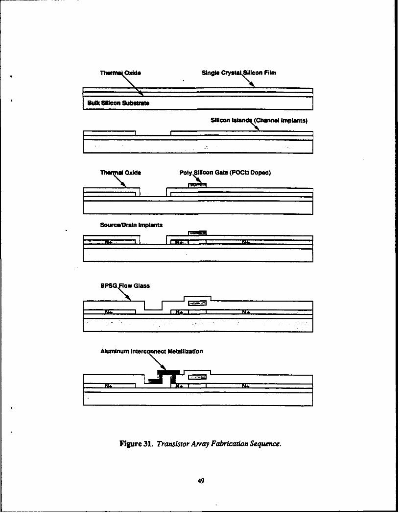
Oxid, Single Clly on Film
Sulk SiloonSueae
Silicon Islan (Channel Implants)
Ohe xlde Poly Silicon Glate (POCMa Doped)
Source/Drain Implants
BPSG Flow Glass
Aluminum Interc nnect Metallization
Figure 31. Transistor Array Fabrication Sequence.
49

After circuit processing, the 2.5- x 2.5-in integrated active matrix display circuit wasremoved from the silicon substrate and permanently bonded to glass using a thin layer of adhesiveas shown schematically in Fig. 32. Both Coming 7059 and Hoya NA-40 glass were csedL As aconequence of the transer process, the original top surface of the circuit is placed adjacent to theglass and the back side of the circuit is exposed. Photolithographic processing is used post-transfer to expose the input contacts. The x-Si circuit is then put through a final test and laserrepair procedure, normally done to the equivalent poly-Si circuits. These tests showed that thetransfer process did not significantly increase the number of defects.
ICs
StandardCWafer . ls
1. Fabricate Circuitsin IC Foundry
S~ICS on Glass
Substrate ••
3. Mount on Glass
Figure 32. Silicon Display Transfer Process.
50
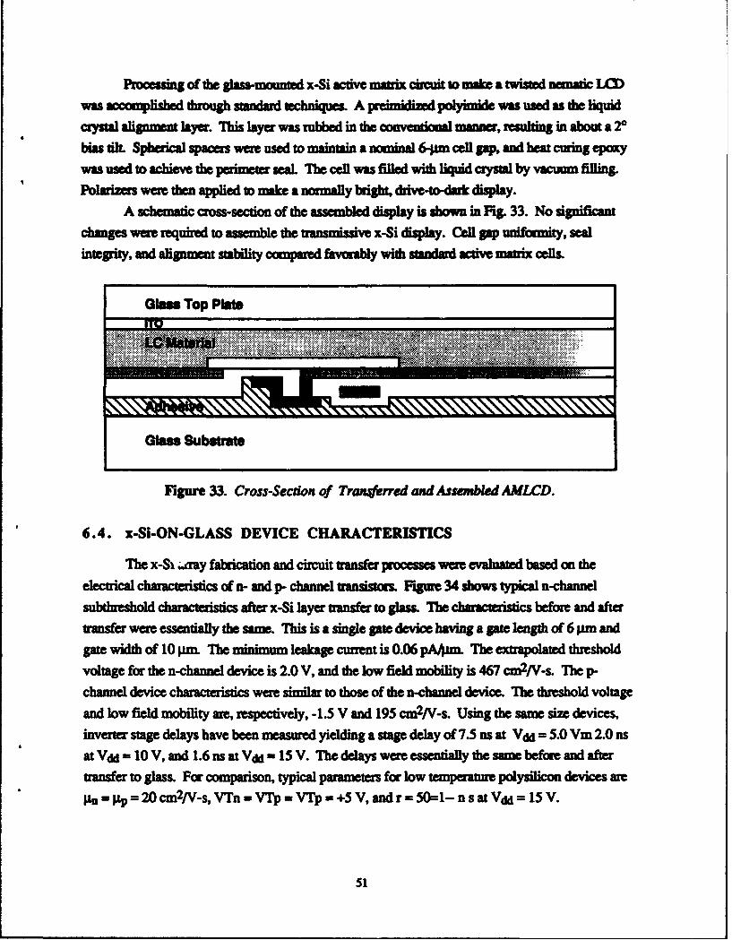
Processing of the gasm nedx-Si active matrx circuit to make a twisted neumac LCDwas accomuplished through, standard techniques. A preimidized polyimuide was used as the liquidcr~ystal alignment layer. This layer was rubbed in the conventional manner, resulting in about a rbias tilt. Spherical spaces were used to maintain a nominal 6-lpm cell gap and heam cluing epoxywas used to achieve the paueriee seal. The cell was filled with liquid crystal by vacuum filling.Pblarizers were then applied to maie a normially bright, drive-to-dark display.
A schematic crosssectio of the assembled disply is shown in Fig. 33. No significant
chages were required to assemble the musmissive x-Si display. Cell gap uniformity, sealintegrity, and alignment stability compared favorably with standard active matrix cells.
FRgur 33. Cross-Seedon of Tra.Vefered and Assemble AMLCD.
6.4. i-Si-ON-GLASS DEVICE CHARACTERISTCS
The x-Si .aray fabrication and circuit transfer processes were evaluated based on theelectrical charcterstics of n- and p- channel trasistors. Figure 34 shows typial n-channelsubthreshold characteristics after x-Si layer trasfer to glass1cI. Th c arateistics before and aftertranser were essentially the same. This is a single gaie device having a gate length of 6 prm andgate width of 10 pm. The minimumn leakage current is 0.06 pA4=m The extrapolated thresholdvoltage for the n-channel device is 2.0V, and the low field mobility is 467 cm2lV-s. The p-channel device chrceits were simila to those of the n-channel device, The threshold voltageand low field mobility are, respectively, -1.5 V and 195 cm2 NV-s. Using the same size devices,inverter stage delays have been measured yielding astage delay of 7.5 ns at Vdd =5.OVmn2.Onsat Vdd = 10 V, and 1.6 ns at V(,d - 15 V. The delays were essentially the same before and aftertransfer to glass. For comparison, typical parameters for low temperaur polysilicon devices arepn =pp =20 cm2/V-s. VTn =VTp =VTp =+5 V,and r=-50=1- ns at Vdd= 15V.
51
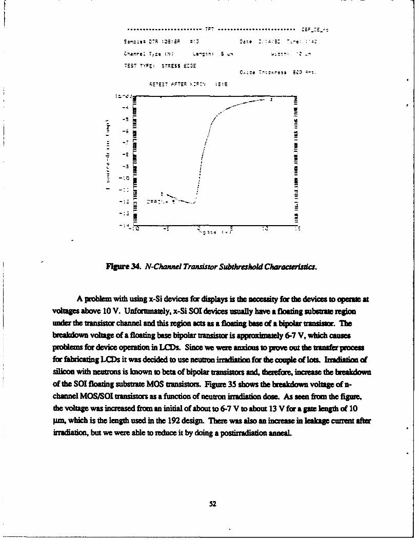
. . ... .. ............... . . . . . ..e ...
T V;C.,::* Tr'-..•rt~s EZI I--:.
-~ S
".-~ - I- -
Figure 34. N-Channel Tranadssor Sub$•tvh l Chracteri.is.
A problem with using x-Si devices for displays is the necessity for the devices to operm atvoltages above 10 V. Unformnately, x-Si SOI devices usually have a floating substrae regionundethe ansi channel and this region ats as a floating boae of a bipolar transis.or. Mhebakdown voltage of a floating base bipolar transistor is apprFinatpy 6-7 V, which causesProblem for device operation in LCDs. Since we were anxious to piro out the uansf a proepsfor fabricating LC(s it was decided to use neutron irradiation for the couple of lotL rradiation ofsilicon with neunrns is known to beta of bipolar transistors and, therefore, increase the breakdownof the SOI floating substrate MOS transistom Figure 35 shows the breakdown voltage of n-channel MOS/SOI transistors as a function of neutron iuradtion dose. As seen firom the figure,the voltage was increased from an initial of about to 6-7 V to about 13 V fora gate length of 10
9rm, which is the length used in the 192 design. There was also an incmse in leakage current afterrradiation, but we were able to reduce it by doing a Postirradiation anneal
52
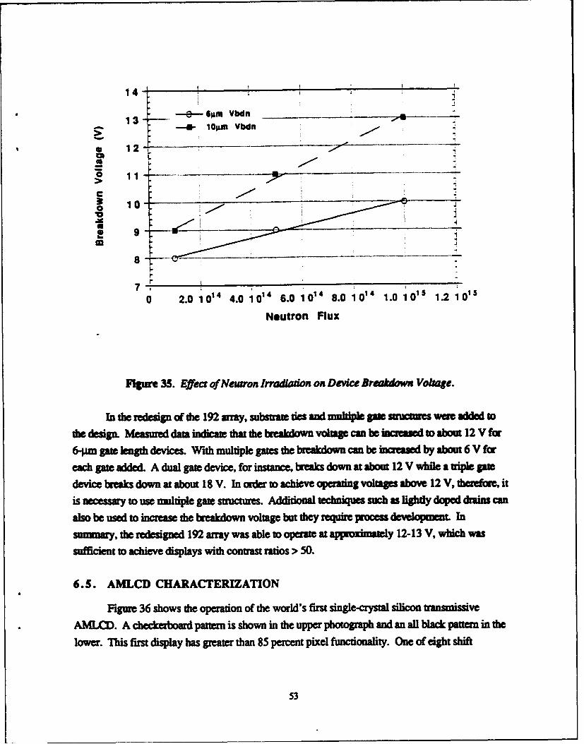
14- ,
1 3 -e-- GILm Vbdn -
12 -, """U- 11-m Vb-
o lo - -:...'
Zi
>
CS 10-
V.
eac 2.0e 10ed A4 d4.0 1014 6evce f1r int4e bre.k 1ow0o4 1.0 lolhle 1. ilollz
device gr 35e.k dow ffecbot of Neutrn Irrader ationhiv opeung D vic laoe 12 V, teVoltagi.
In ne hessry dsi of th 9urmsbtatee multiple game strct• diina eh uchture litl adoded tois a
dieo beusedn Moieasued dthe inict thatghe breakdowy reqtage anobes inceasedlo abut. 12Vo
mmzy the redesigned 192 arrmy was able to operate at panpximtely 12-13 V, which was
sufflicient to achieve displays with contrast ratios > 50.
6.S. AMLCD CHARACTERIZATION
Figure 36 shows the operation of the world's first single-crystal silicon transmissive
A.MIX. A- Jh-keI-az pattern is shown in the upper photograph and an all black pattern in the
lower. This first display has gre~ate than 85 percent pixel fimnctonality. One of eight shift
53
reisters did not operate properly making the left-most 24 colums inoperable. Several d&scre
pixels, mostly rea the right side of the display, were also inoperable. The pixel opens atbelieved to be due to over etching of the transistor conmac during Wy processing and not due ID
either the x-Si circuit transfer process or the LC assembly. The measured corast ratio for this
display, which does not contain a black matrix, is 4.7:1 using a pixel voltage of 4.8-V RMS. The
calculated contrast raio that would have resulted using a black matrix is 20- 1. The display is
normally operated at 180I fims/sec and a data clock rate of I MHz. The display also operates at
the maximum daa clock frequency, which the drive electronics can generate. This ifrequency of 5.5 MHz produces a fume rate of 270 fumessec. This display was assembled fromthe first lot of x-Si wafers and used neutron irradiation to achieve an operating voltage of 12 V.
Figure 37 shows a display from the third and final lot of processed x-Si SO wafers. This
display was fabricated using the modified mask set that contained body ties and multiple gatesauctume No neutron irradiation was used to fabricate this display. As seen from the figure,
there ae no inoperable registers in either the darn or select circuitry and very few pixel defectsThis display was assembled using color filters and is available for -e--nstration at the Sarnoff.
Figure 38 shows micrographs of two different pixel arrays. The top micrograph of a
standard poly-Si AMLCD pixel shows that disclinations (bright curved lines) form along the left
side of the select lines. The disclinations are believed to be due to the fintrcion of the non planar
surface and the electri field adjacent to the select lines. They occur along one side of the select line
in the direction of the alignment layer rubbing. When very small pixels are used in an LCD, the
bright disclnations are a significant contribution to a reduction in contrast ratio. The lower figure
shows the same "all black" pattern on the single crystal transferred display. No diclinations are
observed. The elimination of the disclinations is believed to be due to the planer surface ove the
select lines.
54

Checkerboard"Pattern
All BlackPattern
Figure 36. Photograph of World's First Silicon Transfer AMLCD.
55

T7.~
It'*
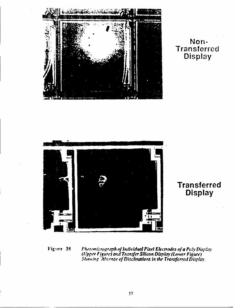
Non-Transferred
Display
TransferredDisplay
~~ .1~ ~~ t ~ ~ph of Individ~wdPixlltrd mkvde !~ a P ly iv M~yI*4~ igate0 n~4mITrxftr Silicon DLhpfYa (LO. me.r Fig.ure71r~p, 1ene D~ivfinworx In the T~a¶ferred, Display,
7. REFERENCES
1. R. Williams, "Domains in Liquid Crystals," J. Chem. Phys. 39. 384 (1963).
2. G. H. Heilmeier, L. A. Zanoni, L A. Barton, "A Flat Liquid Crystal ReflectiveDisplay Based on Dynamic Scattering," Proc. IEEE 56 1162 (1968).
3. B. J. Lechner et aL, "Liquid Crystal Matrix Display," Proc. IEEE W(1 1), November1971.
4. P. K. Weimer, "The TFT - A New Thin Film Transistor," Proc. IRE 0. 1462(1962).
5. C. IL Anderson et aL, "Electron Guides with Extraction, A Potentially Useful NewClass of Electron Devices," IEDjMITchnicaLDig pp. 264-267 (1978).
6. C. A. Camanese and J. Endriz, "The Multiplier-Assisted Discharge: A New Type ofCold Cathode," J. AppL Phys., 5L 2, 731-745 (1979).
7. E. U. Condion, Hugh Odeshaw, ed., Handbook of Physics (New York: McGraw-Hill 1967) pp. 6-62,63.
8. formation in a conversation with the authors from Robert Y. Pai of GTE, SalemMA., November 29, 1989.
9. W. Burt Mercer, James A. Schoke, "Fluorescent Backlights for LCDs," Information
Display, V- 11 (November, 1989), 8-13.
10. Ibid.
11. T. Maxson, et al, "High-Efficiency Light Diffuser for Use in Information Displays,"Application Notes, Session 12, Society for Information Display Conference, Boston(May, 1992), 10-11.
12. K. Sumiyoshi, Y. Sato, S. Kaneko, M. Sakamoto, M. Imai, Y. Kato, S. Wada, H.Kohashi, M. Ashibi, T. Ohmachi, K. Kubota, and N. Endo, Proceedings of the 1989International Electron Devices Meeting (IEEE, New York, 1989) pp. 165-168.
13. P.M. Zavracky, D.P. Vu, L. Allen, W. Henderson, H. Guckel, J.J. Sniegowski,T.P. Ford, and J.C.C. Fan, in "Silicon-on-Insulator and Buried Metals inSemiconductors," C. K. Chen, P.L.F. Hemment, J.C. Starm, and L. Pfeiffer, eds.,Materials Research Society Symposium Proceddings = 1988, pp. 213-219.
14. L.T.P. Allen, M.W. Batty, W.R. Henderson, T.E. Jersey, D.P. Vu, P.M. Zavracky, and J.Narayan, in "Advanced processing of Semicondcutor Devices H," SPIE VoL 945, Society ofPhoto-Optical and Instrumentation Engineers, 1988, pp. 126-130.
15. L.T.P. Allen, P.M. Zavracky, D.P. Vu, M.W. Batty, W.R. Henderson, T.J. Boden, D.K.Bowen, D. Gorden-Smith, C.R. Thomas, and T. Tjahjadi, Materials Research SocietySymposium Proceedings JAL 1989, pp. 213-219.
16. B.W. Faughnan, R. Stewart, A. Ipri, in Proceedings of the SID, Vol. 29, No. 4, 1988, pp.279-282.
58