Embed Size (px)
Citation preview

FUNCTIONAL BLOCK DIAGRAM
(MSB)DB15
DB0(LSB)
CLOCK NC REFCOM REFOUT IREFIN NR
VEE
LADCOM
IOUTB
IOUTA
DCOM VDD
MSBs: SEGMENTEDCURRENT SOURCESAND SWITCHES
MSBDECODER
ANDEDGE-
TRIGGEREDBIT
LATCHES
LSBs:CURRENT SOURCES,SWITCHES, AND1kΩ R-2RLADDERS
AD768
CONTROLAMP
2.5VBANDGAP
REFERENCE
1k1k
REV. B
Information furnished by Analog Devices is believed to be accurate andreliable. However, no responsibility is assumed by Analog Devices for itsuse, nor for any infringements of patents or other rights of third partieswhich may result from its use. No license is granted by implication orotherwise under any patent or patent rights of Analog Devices.
a
FEATURES
30 MSPS Update Rate
16-Bit Resolution
Linearity: 1/2 LSB DNL @ 14 Bits
1 LSB INL @ 14 Bits
Fast Settling: 25 ns Full-Scale Settling to 0.025%
SFDR @ 1 MHz Output: 86 dBc
THD @ 1 MHz Output: 71 dBc
Low Glitch Impulse: 35 pV-s
Power Dissipation: 465 mW
On-Chip 2.5 V Reference
Edge-Triggered Latches
Multiplying Reference Capability
APPLICATIONS
Arbitrary Waveform Generation
Communications Waveform Reconstruction
Vector Stroke Display
16-Bit, 30 MSPSD/A Converter
AD768
PRODUCT DESCRIPTIONThe AD768 is a 16-bit, high speed digital-to-analog converter(DAC) that offers exceptional ac and dc performance. TheAD768 is manufactured on ADI’s Advanced Bipolar CMOS(ABCMOS) process, combining the speed of bipolar transistors,the accuracy of laser-trimmable thin film resistors, and the effi-ciency of CMOS logic. A segmented current source architectureis combined with a proprietary switching technique to reduceglitch energy and maximize dynamic accuracy. Edge triggeredinput latches and a temperature compensated bandgap referencehave been integrated to provide a complete monolithic DACsolution.
The AD768 is a current-output DAC with a nominal full-scaleoutput current of 20 mA and a 1 kΩ output impedance. Differ-ential current outputs are provided to support single-endedor differential applications. The current outputs may be tieddirectly to an output resistor to provide a voltage output, or fedto the summing junction of a high speed amplifier to provide abuffered voltage output. Also, the differential outputs may beinterfaced to a transformer or differential amplifier.
The on-chip reference and control amplifier are configured formaximum accuracy and flexibility. The AD768 can be driven bythe on-chip reference or by a variety of external reference volt-ages based on the selection of an external resistor. An externalcapacitor allows the user to optimally trade off reference band-width and noise performance.
The AD768 operates on ±5 V supplies, typically consuming465 mW of power. The AD768 is available in a 28-pin SOICpackage and is specified for operation over the industrial tem-perature range.
PRODUCT HIGHLIGHTS1. The low glitch and fast settling time provide outstanding
dynamic performance for waveform reconstruction or digitalsynthesis requirements, including communications.
2. The excellent dc accuracy of the AD768 makes it suitable forhigh speed A/D conversion applications.
3. On-chip, edge-triggered input CMOS latches interfacereadily to CMOS logic families. The AD768 can support up-date rates up to 40 MSPS.
4. A temperature compensated, 2.5 V bandgap reference isincluded on-chip allowing for generation of the referenceinput current with the use of a single external resistor. An ex-ternal reference may also be used.
5. The current output(s) of the AD768 may be used singly ordifferentially, either into a load resistor, external op ampsumming junction or transformer.
6. Proper selection of an external resistor and compensationcapacitor allow the performance-conscious user to optimizethe AD768 reference level and bandwidth for the targetapplication.
© Analog Devices, Inc., 1996
One Technology Way, P.O. Box 9106, Norwood, MA 02062-9106, U.S.A.
Tel: 617/329-4700 Fax: 617/326-8703

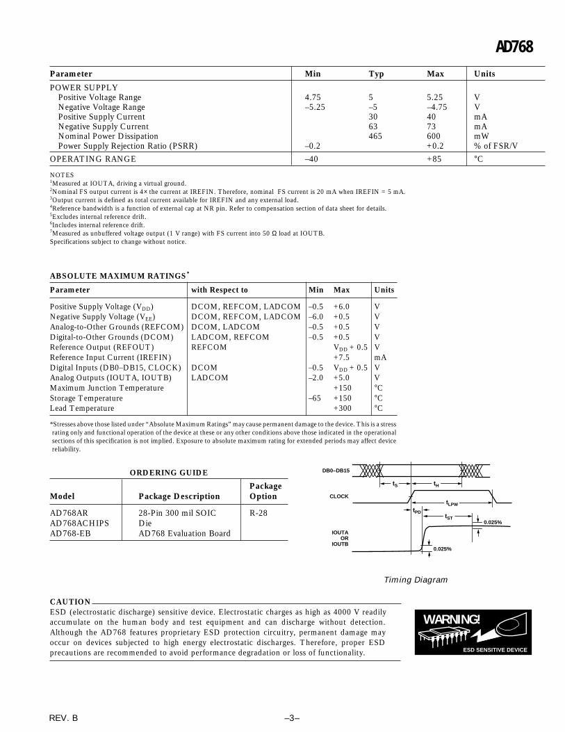
AD768–SPECIFICATIONSParameter Min Typ Max Units
RESOLUTION 16 Bits
DC ACCURACY1
Linearity ErrorTA = +25°C –8 ±4 +8 LSBTMIN to TMAX –8 +8 LSB
Differential NonlinearityTA = +25°C –6 ±2 +6 LSBTMIN to TMAX –8 +8 LSB
Monotonicity (13-Bit) GUARANTEED OVER RATED SPECIFICATION TEMPERATURE RANGE
ANALOG OUTPUTOffset Error –0.2 +0.2 % of FSRGain Error –1.0 +1.0 % of FSRFull-Scale Output Current2 20 mAOutput Compliance Range –1.2 +5.0 VOutput Resistance 0.8 1.0 1.2 kΩOutput Capacitance 3 pF
REFERENCE OUTPUTReference Voltage 2.475 2.5 2.525 VReference Output Current3 +5.0 +15 mA
REFERENCE INPUTReference Input Current 1 5 7 mAReference Bandwidth4
Small Signal, IREF = 5 mA ± 0.1 mA 28 MHzLarge Signal, IREF = 4 mA ± 2 mA 9 MHz
TEMPERATURE COEFFICIENTSUnipolar Offset Drift –5 +5 ppm of FSR/oCGain Drift5 –20 +20 ppm of FSR/oCGain Drift6 –40 +40 ppm of FSR/oCReference Voltage Drift –30 +30 ppm/oC
DYNAMIC PERFORMANCE7
Maximum Output Update Rate 30 40 MSPSOutput Settling Time (tST) (to 0.025%) 25 35 nsOutput Propagation Delay (tPD) 10 nsGlitch Impulse 35 pV-sOutput Rise Time (10% to 90%) 5 nsOutput Fall Time (10% to 90%) 5 nsOutput Noise (DB0–DB15 High, into 50 Ω) 3 nV/√HzDifferential Gain Error 0.01 %Differential Phase Error 0.01 Degree
DIGITAL INPUTSLogic “1” Voltage 3.5 VLogic “0” Voltage 1.5 VLogic “1” Current –10 +10 µALogic “0” Current –10 +10 µAInput Capacitance 10 pFInput Setup Time (tS) 10 nsInput Hold Time (tH) 5 nsLatch Pulse Width (tLPW) 10 ns
AC LINEARITY7
Spurious-Free Dynamic Range (SFDR Within a Window)FOUT = 1.002 MHz; CLOCK = 10 MHz; 2 MHz Span 86 79 dBFOUT = 1.002 MHz; CLOCK = 20 MHz; 2 MHz Span 85 dBFOUT = 5.002 MHz; CLOCK = 30 MHz; 10 MHz Span 78 dB
Spurious-Free Dynamic Range (SFDR to Nyquist)FOUT = 1.002 MHz; CLOCK = 10 MHz 74 70 dBFOUT = 1.002 MHz; CLOCK = 20 MHz 73 dBFOUT = 5.002 MHz; CLOCK = 30 MHz 67 dB
Total Harmonic Distortion (THD)FOUT = 1.002 MHz; CLOCK = 10 MHz –71 –68 dBFOUT = 1.002 MHz; CLOCK = 20 MHz –66 dBFOUT = 5.002 MHz; CLOCK = 30 MHz –61 dB
REV. B–2–
(TMIN to TMAX , VDD = +5.0 V, VEE = –5.0 V, LADCOM, REFCOM, DCOM = 0 V, IREFIN = 5 mA,CLOCK = 10 MHz, unless otherwise noted)
Parameter Min Typ Max Units
POWER SUPPLYPositive Voltage Range 4.75 5 5.25 VNegative Voltage Range –5.25 –5 –4.75 VPositive Supply Current 30 40 mANegative Supply Current 63 73 mANominal Power Dissipation 465 600 mWPower Supply Rejection Ratio (PSRR) –0.2 +0.2 % of FSR/V
OPERATING RANGE –40 +85 °C
NOTES1Measured at IOUTA, driving a virtual ground.2Nominal FS output current is 4× the current at IREFIN. Therefore, nominal FS current is 20 mA when IREFIN = 5 mA.3Output current is defined as total current available for IREFIN and any external load.4Reference bandwidth is a function of external cap at NR pin. Refer to compensation section of data sheet for details.5Excludes internal reference drift.6Includes internal reference drift.7Measured as unbuffered voltage output (1 V range) with FS current into 50 Ω load at IOUTB.Specifications subject to change without notice.
ABSOLUTE MAXIMUM RATINGS*
Parameter with Respect to Min Max Units
Positive Supply Voltage (VDD) DCOM, REFCOM, LADCOM –0.5 +6.0 VNegative Supply Voltage (VEE) DCOM, REFCOM, LADCOM –6.0 +0.5 VAnalog-to-Other Grounds (REFCOM) DCOM, LADCOM –0.5 +0.5 VDigital-to-Other Grounds (DCOM) LADCOM, REFCOM –0.5 +0.5 VReference Output (REFOUT) REFCOM VDD + 0.5 VReference Input Current (IREFIN) +7.5 mADigital Inputs (DB0–DB15, CLOCK) DCOM –0.5 VDD + 0.5 VAnalog Outputs (IOUTA, IOUTB) LADCOM –2.0 +5.0 VMaximum Junction Temperature +150 °CStorage Temperature –65 +150 °CLead Temperature +300 °C
*Stresses above those listed under “Absolute Maximum Ratings” may cause permanent damage to the device. This is a stressrating only and functional operation of the device at these or any other conditions above those indicated in the operationalsections of this specification is not implied. Exposure to absolute maximum rating for extended periods may affect devicereliability.
AD768
REV. B
ORDERING GUIDE
PackageModel Package Description Option
AD768AR 28-Pin 300 mil SOIC R-28AD768ACHIPS DieAD768-EB AD768 Evaluation Board
–3–
tH tS
tLPWtPD
tST0.025%
0.025%
DB0–DB15
CLOCK
IOUTAOR
IOUTB
Timing Diagram
WARNING!
ESD SENSITIVE DEVICE
CAUTIONESD (electrostatic discharge) sensitive device. Electrostatic charges as high as 4000 V readilyaccumulate on the human body and test equipment and can discharge without detection.Although the AD768 features proprietary ESD protection circuitry, permanent damage mayoccur on devices subjected to high energy electrostatic discharges. Therefore, proper ESDprecautions are recommended to avoid performance degradation or loss of functionality.
REV. B–4–
AD768
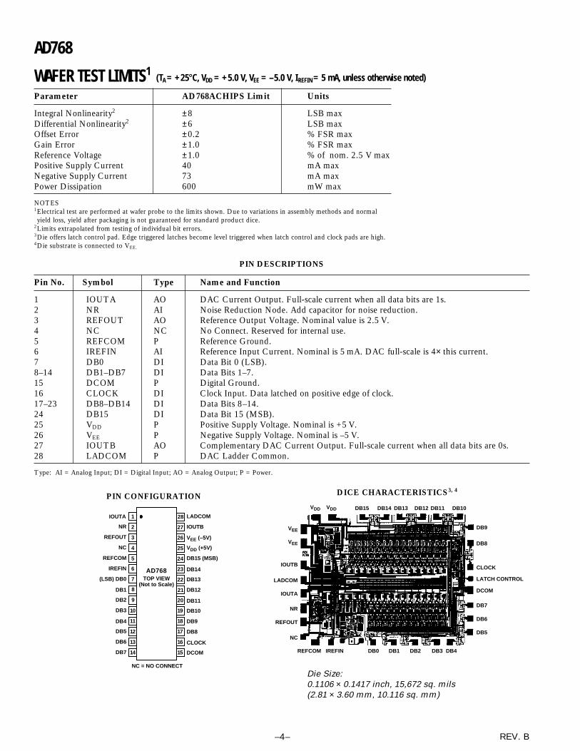
WAFER TEST LIMITS1
Parameter AD768ACHIPS Limit Units
Integral Nonlinearity2 ±8 LSB maxDifferential Nonlinearity2 ±6 LSB maxOffset Error ±0.2 % FSR maxGain Error ±1.0 % FSR maxReference Voltage ±1.0 % of nom. 2.5 V maxPositive Supply Current 40 mA maxNegative Supply Current 73 mA maxPower Dissipation 600 mW max
NOTES1Electrical test are performed at wafer probe to the limits shown. Due to variations in assembly methods and normalyield loss, yield after packaging is not guaranteed for standard product dice.
2Limits extrapolated from testing of individual bit errors.3Die offers latch control pad. Edge triggered latches become level triggered when latch control and clock pads are high.4Die substrate is connected to VEE.
PIN DESCRIPTIONS
Pin No. Symbol Type Name and Function
1 IOUTA AO DAC Current Output. Full-scale current when all data bits are 1s.2 NR AI Noise Reduction Node. Add capacitor for noise reduction.3 REFOUT AO Reference Output Voltage. Nominal value is 2.5 V.4 NC NC No Connect. Reserved for internal use.5 REFCOM P Reference Ground.6 IREFIN AI Reference Input Current. Nominal is 5 mA. DAC full-scale is 4× this current.7 DB0 DI Data Bit 0 (LSB).8–14 DB1–DB7 DI Data Bits 1–7.15 DCOM P Digital Ground.16 CLOCK DI Clock Input. Data latched on positive edge of clock.17–23 DB8–DB14 DI Data Bits 8–14.24 DB15 DI Data Bit 15 (MSB).25 VDD P Positive Supply Voltage. Nominal is +5 V.26 VEE P Negative Supply Voltage. Nominal is –5 V.27 IOUTB AO Complementary DAC Current Output. Full-scale current when all data bits are 0s.28 LADCOM P DAC Ladder Common.
Type: AI = Analog Input; DI = Digital Input; AO = Analog Output; P = Power.
(TA = +258C, VDD = +5.0 V, VEE = –5.0 V, IREFIN = 5 mA, unless otherwise noted)
VDD VDD DB15 DB14 DB13 DB12 DB11 DB10
REFCOM IREFIN DB0 DB1 DB2 DB3 DB4
VEE
VEE
IOUTB
LADCOM
IOUTA
NR
REFOUT
NC
DB9
DB8
CLOCK
LATCH CONTROL
DCOM
DB7
DB6
DB5
Die Size:0.1106 × 0.1417 inch, 15,672 sq. mils(2.81 × 3.60 mm, 10.116 sq. mm)
DICE CHARACTERISTICS3, 4PIN CONFIGURATION
14
13
12
11
17
16
15
20
19
18
10
9
8
1
2
3
4
7
6
5
TOP VIEW(Not to Scale)
28
27
26
25
24
23
22
21
AD768
NC = NO CONNECT
IOUTA
VDD (+5V)
VEE (–5V)
IOUTB
LADCOM
NR
REFOUT
NC
DB13
DB14
DB15 (MSB)REFCOM
IREFIN
(LSB) DB0
DB1
DB2
DB3 DB10
DB11
DB12
DB4
DB5
DB6
DB7
DB9
DCOM
CLOCK
DB8

AD768
REV. B –5–
Temperature DriftTemperature drift is specified as the maximum change from theambient (+25°C) value to the value at either TMIN or TMAX. Foroffset and gain drift, the drift is reported in ppm of full-scalerange (FSR) per degree C. For reference drift, the drift is re-ported in ppm per degree C.
Power Supply RejectionThe maximum change in the full-scale output as the suppliesare varied from nominal to minimum and maximum specifiedvoltages.
Settling TimeThe time required for the output to reach and remain within aspecified error band about its final value, measured from thestart of the output transition.
Spurious-Free Dynamic RangeThe difference, in dB, between the rms amplitude of theinput signal and the peak spurious signal over the specifiedbandwidth.
Total Harmonic DistortionTHD is the ratio of the rms sum of the first six harmonic com-ponents to the rms value of the measured input signal. It is ex-pressed as a percentage or in decibels (dB).
Glitch ImpulseAsymmetrical switching times in a DAC give rise to undesiredoutput transients which are quantified by a glitch impulse. It isspecified as the net area of the glitch in pV-sec.
DEFINITIONS OF SPECIFICATIONSLinearity Error (Also Called Integral Nonlinearity or INL)Linearity error is defined as the maximum deviation of the ac-tual analog output from the ideal output, determined by astraight line drawn from zero to full scale.
Differential Nonlinearity (or DNL)DNL is the measure of the variation in analog value, normalizedto full scale, associated with a 1 LSB change in digital input code.
MonotonicityA D/A converter is monotonic if the output either increases orremains constant as the digital input increases.
Offset ErrorThe deviation of the output current from the ideal of zero iscalled offset error. For IOUTA, 0 mA output is expected whenthe inputs are all 0s. For IOUTB, 0 mA output is expectedwhen all inputs are set to 1s.
Gain ErrorThe difference between the actual and ideal output span. Theactual span is determined by the output when all inputs are setto 1s minus the output when all inputs are set to 0s. The idealoutput current span is 4× the current applied to the IREFIN pin.
Output Compliance RangeThe range of allowable voltage at the output of a current-outputDAC. Operation beyond the maximum compliance limits maycause either output stage saturation or breakdown, resulting innonlinear performance.
5mA
6
CREFCOMP
1µFRREF500Ω
REFINREFOUTNCVDD
34
+2.5V REF25
5REFCOM
1µF
CNR
2NR
VEE26
15
1µF
1µF
+5V
–5V
DCOM
RLAD1kΩ
RLAD1kΩ
IOUTA
IOUTB
LADCOM
1
28
27
50Ω RLOAD50Ω
IOUTA
IOUTB
SEGMENTEDCURRENTSOURCES
CURRENT SOURCESAND R-2R LADDER
CLOCK
21222324 1920 13141718 789101112
LATCHES – LOWER 12 BITS16MSB DECODE& LATCHES
CLOCK
DB
15
DB
14
DB
13
DB
12
DB
11
DB
10
DB
9
DB
8
DB
7
DB
6
DB
5
DB
4
DB
3
DB
2
DB
1
DB
0
AD768
Figure 1. Functional Block Diagram and Basic Hookup
FUNCTIONAL DESCRIPTIONThe AD768 is a current-output DAC with a nominal full-scalecurrent of 20 mA and a 1 kΩ output impedance. Differentialoutputs are provided to support single-ended or differentialapplications. The DAC architecture combines segmented cur-rent sources for the top four bits (MSBs) and a 1 kΩ R-2R lad-der for the lower 12 bits (LSBs). The DAC current sources areimplemented with laser-trimmable thin film resistors for excel-lent dc linearity. A proprietary switching technique is utilized toreduce glitch energy and maximize dynamic accuracy.
The digital interface offers CMOS compatible edge-triggeredinput latches that interface readily to CMOS logic and supportsclock rates up to 40 MSPS. A temperature compensated 2.5 Vbandgap reference is integrated on-chip to drive the AD768 ref-erence input current with the use of a single external resistor.The functional block diagram in Figure 1 is a simple representa-tion of the internal circuitry to aid the understanding of theAD768’s operation. The DAC transfer function is described,and followed by a detailed description of each key portion of thecircuit. Typical circuit configurations are shown in the sectionAPPLYING THE AD768.
REV. B–6–
AD768
IREFIN – mA
PO
WE
R –
mW
550
500
3001.0 7.02.0 3.0 4.0 5.0 6.0
450
400
350
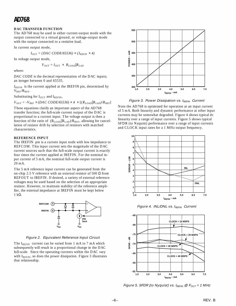
Figure 3. Power Dissipation vs. IREFIN Current
Note the AD768 is optimized for operation at an input currentof 5 mA. Both linearity and dynamic performance at other inputcurrents may be somewhat degraded. Figure 4 shows typical dclinearity over a range of input currents. Figure 5 shows typicalSFDR (to Nyquist) performance over a range of input currentsand CLOCK input rates for a 1 MHz output frequency.
ER
RO
R –
LS
B
IREFIN – mA
10
01.0 7.02.0 3.0 4.0 5.0 6.0
9
6
3
2
1
8
7
5
4INL
DNL
Figure 4. INL/DNL vs. IREFIN Current
IREFIN – mA
SF
DR
– d
B
–85
–551.0 7.02.0 3.0 4.0 5.0 6.0
–80
–75
–70
–65
–60
CLOCK = 10 MSPS
CLOCK = 20 MSPS
CLOCK = 30 MSPS
CLOCK = 40 MSPS
Figure 5. SFDR (to Nyquist) vs. IREFIN @ FOUT = 1 MHz
DAC TRANSFER FUNCTIONThe AD768 may be used in either current-output mode with theoutput connected to a virtual ground, or voltage-output modewith the output connected to a resistive load.
In current output mode,
IOUT = (DAC CODE/65536) × (IREFIN × 4)
In voltage output mode,
VOUT = IOUT × RLOADiRLAD
where:
DAC CODE is the decimal representation of the DAC inputs;an integer between 0 and 65535.
IREFIN is the current applied at the IREFIN pin, determined byVREF/RREF.
Substituting for IOUT and IREFIN,
VOUT = –VREF × (DAC CODE/65536) × 4 × [(RLOADiRLAD)/RREF]
These equations clarify an important aspect of the AD768transfer function; the full-scale current output of the DAC isproportional to a current input. The voltage output is then afunction of the ratio of (RLOADiRLAD)/RREF, allowing for cancel-lation of resistor drift by selection of resistors with matchedcharacteristics.
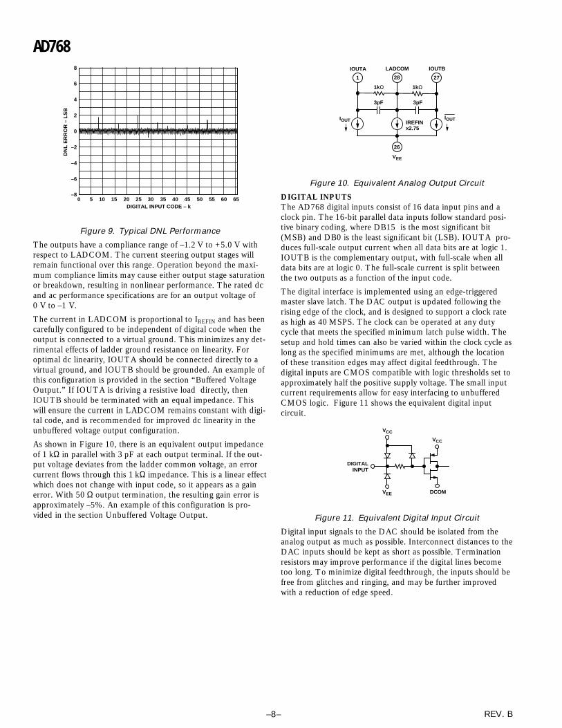
REFERENCE INPUTThe IREFIN pin is a current input node with low impedance toREFCOM. This input current sets the magnitude of the DACcurrent sources such that the full-scale output current is exactlyfour times the current applied at IREFIN. For the nominal in-put current of 5 mA, the nominal full-scale output current is20 mA.
The 5 mA reference input current can be generated from theon-chip 2.5 V reference with an external resistor of 500 Ω fromREFOUT to IREFIN. If desired, a variety of external referencevoltages may be used based on the selection of an appropriateresistor. However, to maintain stability of the reference ampli-fier, the external impedance at IREFIN must be kept below1 kΩ.
5
6
REFCOM
IREFIN
VEE VEE
IFB5mA
Figure 2. Equivalent Reference Input Circuit
The IREFIN current can be varied from 1 mA to 7 mA whichsubsequently will result in a proportional change in the DACfull-scale. Since the operating currents within the DAC varywith IREFIN, so does the power dissipation. Figure 3 illustratesthat relationship.

AD768
REV. B –7–
REFERENCE OUTPUTThe internal 2.5 V bandgap reference is provided for generationof the IREFIN current, and must be compensated externally witha capacitor of 0.1 µF or greater from REFOUT to REFCOM. Ifan external reference is used, REFOUT should be tied directlyto the positive supply voltage, VDD. This effectively turns off theinternal reference, eliminating the need for the external capaci-tor at REFOUT. The reference is specified to drive a nominalload of 5 mA with a maximum of 15 mA. Operation with aheavier load will result in degradation of supply rejection andreference voltage accuracy. Therefore, the reference outputshould be buffered with an amplifier when additional load cur-rent is required. A properly sized pull-up resistor can also beused to source additional current to the load. The resistors valueshould be selected such that REFOUT will always source aminimum of 5 mA to IREFIN and the additional load.
AD768IREFIN
REFOUT
REFCOM
CREFCOMP1µF
500Ω
5
3
6
Figure 6. Typical Reference Hookup
TEMPERATURE CONSIDERATIONSNote that the reference plays a key role in the overall tempera-ture performance of the AD768. Any drift of IREFIN shows updirectly in IOUT. When the output is taken as a current, the driftof IREFIN (which depends on both VREF and RREF) must be mini-mized. This can be done by using the internal temperature com-pensated reference for VREF and a low temperature coefficientresistor for RREF. If the output is taken as a voltage, it is a func-tion of a resistor ratio, not an absolute resistor value. By select-ing resistors with matched temperature coefficients for RREF
and RLOAD, the drift in the resistor values will cancel, providingoptimal drift performance.
REFERENCE NOISE REDUCTION AND MULTIPLYINGBANDWIDTHFor application flexibility and multiplying capabilities, the refer-ence amplifier is designed to offer adjustable bandwidth that canbe reduced by connecting an external capacitor from the NRnode to the negative supply pin, VEE. This capacitor limits thebandwidth and acts as a filter to reduce the noise contributionfrom the reference amplifier.
The noise reduction capacitor, CNR, is not required for stabilityand does not affect the settling time of the DAC output. With-out this capacitor, the IREFIN bandwidth is 15 MHz allowinghigh frequency modulation of the DAC full-scale range throughthe reference input node. Figure 7 shows the relationship be-tween the external noise reduction capacitor and the –3 dBbandwidth of the reference amplifier.
NOISE REDUCTION CAPACITOR – F
BA
ND
WID
TH
– H
z
100M
1k10p 1µ100p 1n 10n 100n
10M
1M
100k
10k
Figure 7. External Noise Reduction Capacitor vs. –3 dBBandwidth
The sensitivity of the NR node requires that care be taken incapacitor placement. The capacitor should be located as physi-cally close to the package pins as possible and lead lengthsshould be minimized. For this purpose, the use of a chipcapacitor is recommended. For applications that do not requirehigh frequency modulation at IREFIN, it is recommended thata capacitor on the order of 1 µF be connected from NR to VEE.If the reference input is purely dc, noise may be minimized withmultiple capacitors, such as 1 µF and 0.1 µF, to more effectivelyfilter both high and low frequency disturbances.
ANALOG OUTPUTSThe AD768 offers two analog outputs; IOUTA is trimmed foroptimal INL and DNL performance and has a full-scale outputwhen all bits are high. For applications that require the specifieddc accuracy, IOUTA should be used. IOUTB is the comple-mentary output with full-scale output when all bits are low.Both IOUTA and IOUTB provide similar dynamic perfor-mance. Refer to Figures 8 and 9 for typical INL and DNL per-formance curves. The outputs can also be used differentially.Refer to the section “Applying the AD768” for examples of vari-ous output configurations.
DIGITAL INPUT CODE – k
8
–80 6510 20 30 40
4
–2
–4
–6
6
0
2
INL
ER
RO
R –
LS
B
50 605 15 25 35 45 55
Figure 8. Typical INL Performance
REV. B–8–
AD768
DIGITAL INPUT CODE – k
8
–80 6510 20 30 40
4
–2
–4
–6
6
0
2
DN
L E
RR
OR
– L
SB
50 605 15 25 35 45 55
Figure 9. Typical DNL Performance
The outputs have a compliance range of –1.2 V to +5.0 V withrespect to LADCOM. The current steering output stages willremain functional over this range. Operation beyond the maxi-mum compliance limits may cause either output stage saturationor breakdown, resulting in nonlinear performance. The rated dcand ac performance specifications are for an output voltage of0 V to –1 V.
The current in LADCOM is proportional to IREFIN and has beencarefully configured to be independent of digital code when theoutput is connected to a virtual ground. This minimizes any det-rimental effects of ladder ground resistance on linearity. Foroptimal dc linearity, IOUTA should be connected directly to avirtual ground, and IOUTB should be grounded. An example ofthis configuration is provided in the section “Buffered VoltageOutput.” If IOUTA is driving a resistive load directly, thenIOUTB should be terminated with an equal impedance. Thiswill ensure the current in LADCOM remains constant with digi-tal code, and is recommended for improved dc linearity in theunbuffered voltage output configuration.
As shown in Figure 10, there is an equivalent output impedanceof 1 kΩ in parallel with 3 pF at each output terminal. If the out-put voltage deviates from the ladder common voltage, an errorcurrent flows through this 1 kΩ impedance. This is a linear effectwhich does not change with input code, so it appears as a gainerror. With 50 Ω output termination, the resulting gain error isapproximately –5%. An example of this configuration is pro-vided in the section Unbuffered Voltage Output.
1
26
2728
1kΩ 1kΩ
3pF 3pF
IOUT IOUTIREFINx2.75
VEE
LADCOM IOUTBIOUTA
Figure 10. Equivalent Analog Output Circuit
DIGITAL INPUTSThe AD768 digital inputs consist of 16 data input pins and aclock pin. The 16-bit parallel data inputs follow standard posi-tive binary coding, where DB15 is the most significant bit(MSB) and DB0 is the least significant bit (LSB). IOUTA pro-duces full-scale output current when all data bits are at logic 1.IOUTB is the complementary output, with full-scale when alldata bits are at logic 0. The full-scale current is split betweenthe two outputs as a function of the input code.
The digital interface is implemented using an edge-triggeredmaster slave latch. The DAC output is updated following therising edge of the clock, and is designed to support a clock rateas high as 40 MSPS. The clock can be operated at any dutycycle that meets the specified minimum latch pulse width. Thesetup and hold times can also be varied within the clock cycle aslong as the specified minimums are met, although the locationof these transition edges may affect digital feedthrough. Thedigital inputs are CMOS compatible with logic thresholds set toapproximately half the positive supply voltage. The small inputcurrent requirements allow for easy interfacing to unbufferedCMOS logic. Figure 11 shows the equivalent digital inputcircuit.
VCC
VEE
DIGITALINPUT
VCC
DCOM
Figure 11. Equivalent Digital Input Circuit
Digital input signals to the DAC should be isolated from theanalog output as much as possible. Interconnect distances to theDAC inputs should be kept as short as possible. Terminationresistors may improve performance if the digital lines becometoo long. To minimize digital feedthrough, the inputs should befree from glitches and ringing, and may be further improvedwith a reduction of edge speed.
AD768
REV. B –9–
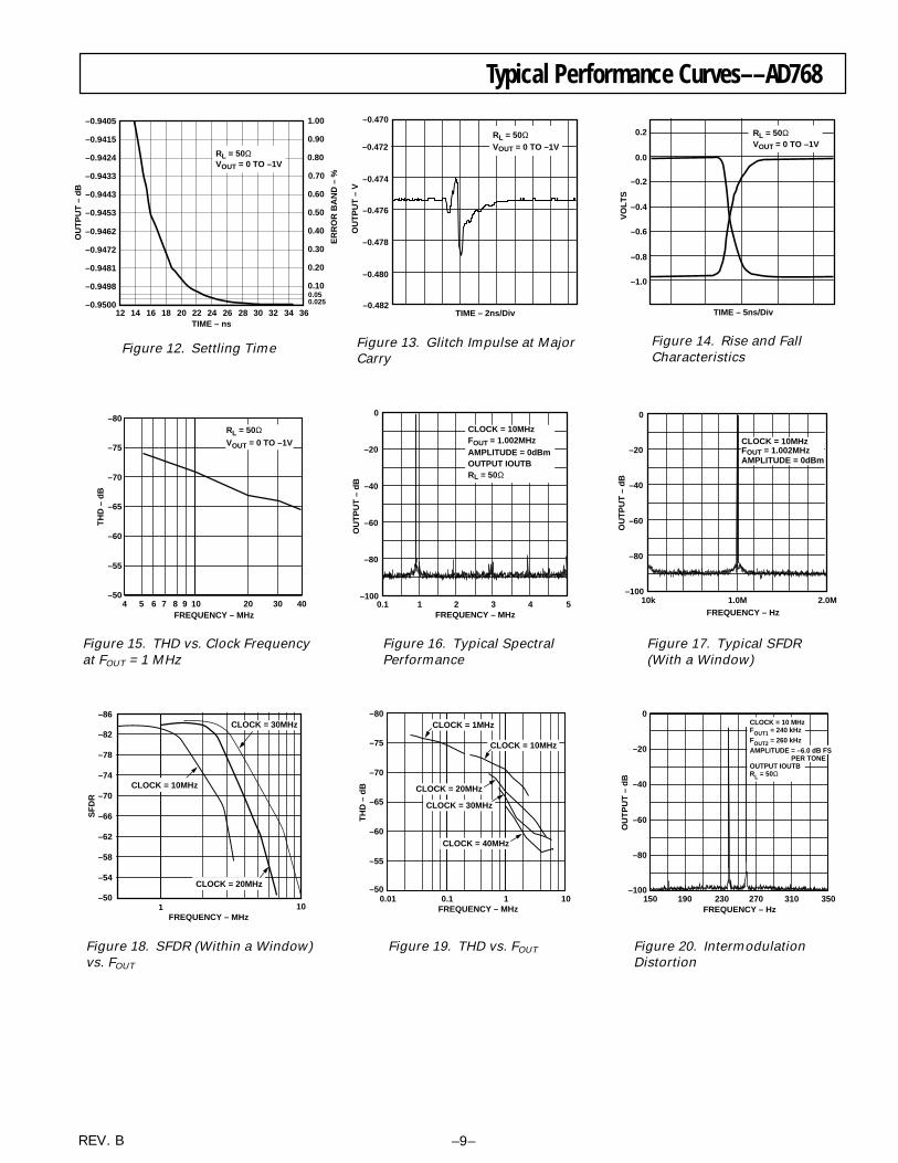
Typical Performance Curves––AD768
0.2
0.0
–0.2
–0.4
–0.6
–0.8
–1.0
VO
LT
S
TIME – 5ns/Div
RL = 50ΩVOUT = 0 TO –1V
Figure 14. Rise and FallCharacteristics
10k 2.0M1.0M
OU
TP
UT
– d
BFREQUENCY – Hz
CLOCK = 10MHzFOUT = 1.002MHzAMPLITUDE = 0dBm
0
–20
–40
–60
–80
–100
Figure 17. Typical SFDR(With a Window)
FREQUENCY – Hz
OU
TP
UT
– d
B
0
–100150 350190 230 270 310
–60
–80
–40
–20
CLOCK = 10 MHzFOUT1 = 240 kHzFOUT2 = 260 kHzAMPLITUDE = –6.0 dB FS PER TONEOUTPUT IOUTBRL = 50Ω
Figure 20. IntermodulationDistortion
RL = 50ΩVOUT = 0 TO –1V
–0.470
–0.472
–0.474
–0.476
–0.478
–0.480
–0.482
OU
TP
UT
– V
TIME – 2ns/Div
Figure 13. Glitch Impulse at MajorCarry
50.1 32 41
OU
TP
UT
– d
B
FREQUENCY – MHz
0
–20
–40
–60
–80
–100
CLOCK = 10MHz FOUT = 1.002MHz AMPLITUDE = 0dBm OUTPUT IOUTB RL = 50Ω
Figure 16. Typical SpectralPerformance
FREQUENCY – MHz
TH
D –
dB
–80
–75
–500.01 0.1 101
–65
–60
–55
–70
CLOCK = 1MHz
CLOCK = 10MHz
CLOCK = 20MHz
CLOCK = 30MHz
CLOCK = 40MHz
Figure 19. THD vs. FOUT
Figure 12. Settling Time
FREQUENCY – MHz
–80
–75
–504 20 40
TH
D –
dB
–65
–60
–55
–70
5 6 7 8 9 10 30
RL = 50ΩVOUT = 0 TO –1V
Figure 15. THD vs. Clock Frequencyat FOUT = 1 MHz
1 10FREQUENCY – MHz
CLOCK = 30MHz
CLOCK = 20MHz
–86
–82
–50
–78
–74
–70
–66
–62
–58
–54
SF
DR
CLOCK = 10MHz
Figure 18. SFDR (Within a Window)vs. FOUT
–0.9405
–0.9443
–0.9415
–0.9424
–0.9433
–0.9453
–0.9500
–0.9462
–0.9472
–0.9498
–0.9481
12 24 3614 16 18 20 22 3426 28 30 32
1.00
0.60
0.90
0.80
0.70
0.50
0.10
0.40
0.30
0.20
0.0250.05
OU
TP
UT
– d
B
ER
RO
R B
AN
D –
%TIME – ns
RL = 50ΩVOUT = 0 TO –1V

REV. B–10–
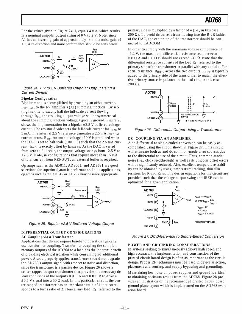
AD768APPLYING THE AD768OUTPUT CONFIGURATIONSThe following sections illustrate some typical output configura-tions for the AD768. While most figures take the output atIOUTA, IOUTB can be interchanged in all cases. Unless other-wise noted, it is assumed that IREFIN and full-scale currents areset to nominal values.
For application that require the specified dc accuracies, properresistor selection is required. In addition to absolute resistor tol-erances, resistor self-heating can result in unexpected errors. Foroptimal INL, the buffered voltage output is recommended asshown in Figure 23. In this configuration, self-heating of RFB
may cause a change in gain, producing a bow in the INL curve.This effect can be minimized by selection of a low temperaturecoefficient resistor.
UNBUFFERED VOLTAGE OUTPUT CONFIGURATIONSFigure 21 shows the AD768 configured to provide a unipolaroutput range of approximately 0 V to –1 V. The nominal full-scale current of 20 mA flows through the parallel combinationof the 50 Ω RL resistor and the 1 kΩ DAC output resistance(from the R-2R ladder), for a combined 47.6 Ω. This producesan ideal full-scale voltage of –0.952 V with respect to LADCOM.In addition, the 1 kΩ DAC output resistance has a tolerance of±20% which may vary the full-scale gain by ±1%. This linearvariation results in a gain error which can be easily compensatedfor by adjusting IREFIN.
1
27
28
VA
VB
AD768
RL49.9Ω
RL49.9Ω
IOUTA
LADCOM
IOUTB
Figure 21. 0 V to –1 V Unbuffered Voltage Output
In this configuration, it is important to note the restrictions fromthe output compliance limits. The maximum negative voltagecompliance is –1.2 V, prohibiting use of a 100 Ω load to producea 0 V to –2 V output swing. One additional consideration foroperation in this mode is integral nonlinearity. As the voltage atthe output node changes, the finite output impedance of theDAC current steering switches gives rise to small changes in theoutput current that vary with output voltage, producing a bow(up to 8 LSBs) in the INL. For optimal INL performance, thebuffered voltage output mode is recommended.
The INL is also slightly dependent on the termination of theunused output (IOUTB) as described in the ANALOG OUT-PUT section. To eliminate this effect, IOUTB should be termi-nated with the same impedance as IOUTA, so both outputs seethe same resistive divider to ground. This will keep the currentin LADCOM constant, minimizing any code-dependent IRdrops within the DAC ladder that may give rise to additionalnonlinearities.
AC-Coupled OutputConfiguring the output as shown in Figure 22 provides a bipolaroutput signal from the AD768 without requiring the use of asumming amplifier. The ac load impedance presented to the
DAC output is the parallel combination of the AD768’s outputimpedance, RL, and bias resistor RB. The nominal output swingwith the values given in Figure 22 is ±0.5 V assuming RB >> RL.The gain of the circuit will be a function of the tolerances of theimpedances RLAD, RB, and RL.
Choosing the value of RB and C will depend primarily on thedesired –3 dB high pass cutoff frequency and the bias current,IB, of the subsequent stage connected to RB. The –3 dB fre-quency can be approximated by the equation,
f–3 dB = 1/[2 × π × (RB + RLiRLAD) × C].
The dc offset of the output is a function of the bias current ofthe subsequent stage and the value of RB. For example, ifC = 390 pF, RB = 20 kΩ, and IB = 1.0 µA, the –3 dB frequencyis approximately 20.4 kHz and the dc offset would be 20 mV.
1
27
28
RB
AD768
RL49.9Ω
IOUTA
LADCOM
IOUTBRL49.9Ω
IBC
Figure 22. 0.5 V to –0.5 V Unbuffered AC-Coupled Output
BUFFERED VOLTAGE OUTPUT CONFIGURATIONSUnipolar ConfigurationFor positive output voltages, or voltage ranges greater thanallowed by output compliance limits, some type of externalbuffer is needed. A wide variety of amplifiers may be selectedbased on considerations such as speed, accuracy and cost. TheAD9631 is an excellent choice when dynamic performance isimportant, offering low distortion up to 10 MHz. Figure 23shows the implementation of 0 V to +2 V full-scale unipolarbuffered voltage output. The amplifier establishes a summingnode at ground for the DAC output. The buffered output volt-age results from the DAC output current flowing through theamplifier’s feedback resistor, RFB. In this case, the 20 mA full-scale current across RFB (100 Ω) produces an output voltagerange of 0 V through +2 V. The same configuration using a pre-cision amplifier such as the AD845 is recommended for optimaldc linearity.
1
27
28
AD768
RFB100Ω
IOUTA
LADCOM
IOUTB
A1
Figure 23. Unipolar 0 V to +2 V Buffered Voltage Output
Buffered Output Using a Current DividerThe configuration shown in Figure 23 may not be possible incases where the amplifier cannot supply the requisite 20 mAfeedback current. As an alternative, Figure 24 shows amplifierA1 in conjunction with a resistive current divider. The values ofRFF and RL are chosen to limit the current, I3, which must besupplied by A1. Current, I2, is shunted to ground through resis-tor, RL. The parallel combination of RFF and RL should not ex-ceed 60 Ω to avoid exceeding the specified compliance voltage.
AD768
REV. B –11–
For the values given in Figure 24, I3 equals 4 mA, which resultsin a nominal unipolar output swing of 0 V to 2 V. Note, sinceA1 has an inverting gain of approximately –4 and a noise gain of+5, A1’s distortion and noise performance should be considered.
1
27
28
AD768
RFB500Ω
IOUTA
LADCOM
IOUTB
RFF100Ω
RL24.9Ω
RP20Ω
I1
I2
I3
A1
Figure 24. 0 V to 2 V Buffered Unipolar Output Using aCurrent Divider
Bipolar ConfigurationBipolar mode is accomplished by providing an offset current,IBIPOLAR, to the I/V amplifier’s (A1) summing junction. By set-ting IBIPOLAR to exactly half the full-scale current flowingthrough RFB, the resulting output voltage will be symmetricalabout the summing junction voltage, typically ground. Figure 25shows the implementation for a bipolar ±2.5 V buffered voltageoutput. The resistor divider sets the full-scale current for IDAC to5 mA. The internal 2.5 V reference generates a 2.5 mA IBIPOLAR
current across RBIP. An output voltage of 0 V is produced whenthe DAC is set to half scale (100. . .0) such that the 2.5 mA cur-rent, IDAC, is exactly offset by IBIPOLAR. As the DAC is variedfrom zero to full-scale, the output voltage swings from –2.5 V to+2.5 V. Note, in configurations that require more than 15 mAof total current from REFOUT, an external buffer is required.
Op amps such as the AD811, AD8001, and AD9631 are goodselections for superior dynamic performance. In dc applications,op amps such as the AD845 or AD797 may be more appropriate.
27
AD768RFB1kΩ
IOUTA
LADCOM
IOUTB
75Ω
24.9ΩRP20Ω
A1
C3
IBIPOLAR
RBIP1kΩ
REFOUT
IDAC
28
1
Figure 25. Bipolar ±2.5 V Buffered Voltage Output
DIFFERENTIAL OUTPUT CONFIGURATIONSAC Coupling via a TransformerApplications that do not require baseband operation typicallyuse transformer coupling. Transformer coupling the comple-mentary outputs of the AD768 to a load has the inherent benefitof providing electrical isolation while consuming no additionalpower. Also, a properly applied transformer should not degradethe AD768’s output signal with respect to noise and distortion,since the transformer is a passive device. Figure 26 shows acenter-tapped output transformer that provides the necessary dcload conditions at the outputs IOUTA and IOUTB to drive a±0.5 V signal into a 50 Ω load. In this particular circuit, the cen-ter-tapped transformer has an impedance ratio of 4 that corre-sponds to a turns ratio of 2. Hence, any load, RL, referred to the
primary side is multiplied by a factor of 4 (i.e., in this case200 Ω). To avoid dc current from flowing into the R-2R ladderof the DAC, the center tap of the transformer should be con-nected to LADCOM.
In order to comply with the minimum voltage compliance of–1.2 V, the maximum differential resistance seen betweenIOUTA and IOUTB should not exceed 240 Ω. Note that thedifferential resistance consists of the load RL, referred to theprimary side of the transformer in parallel with any added differ-ential resistance, RDIFF, across the two outputs. RDIFF is typicallyadded to the primary side of the transformer to match the effec-tive primary source impedance to the load (i.e., in this case200 Ω).
1
27
AD768IOUTA
LADCOM
IOUTB
RDIFF200Ω
T1 RL50Ω
4:1 IMPEDANCERATIO
T1 = MINI-CIRCUITS T4-6T28
Figure 26. Differential Output Using a Transformer
DC COUPLING VIA AN AMPLIFIERA dc differential to single-ended conversion can be easily ac-complished using the circuit shown in Figure 27. This circuitwill attenuate both ac and dc common-mode error sources dueto the differential nature of the circuit. Thus, common-modenoise (i.e., clock feedthrough) as well as dc unipolar offset errorswill be significantly reduced. Also, excellent temperature stabil-ity can be obtained by using temperature tracking, thin filmresistors for R and RREF. The design equations for the circuit areprovided such that the voltage output swing and IREF can beoptimized for a given application.
1
27
28
AD768R*
IOUTA
LADCOM
IOUTB
RREF* IREF
A1
R*
6
3REFOUT
REFIN
VOUT
VOUT = ±4 IREF R
WHERE IREF = 2.5VRREF
VOUT ± 2VR = 200ΩRREF = 5 x 200Ω
*OHMTEK TDP-1403
Figure 27. DC Differential to Single-Ended Conversion
POWER AND GROUNDING CONSIDERATIONSIn systems seeking to simultaneously achieve high speed andhigh accuracy, the implementation and construction of theprinted circuit board design is often as important as the circuitdesign. Proper RF techniques must be used in device selection,placement and routing, and supply bypassing and grounding.
Maintaining low noise on power supplies and ground is criticalto obtaining optimum results from the AD768. Figure 28 pro-vides an illustration of the recommended printed circuit boardground plane layout which is implemented on the AD768 evalu-ation board.

REV. B–12–
AD768
Figure 28. Printed Circuit Board Ground Plane Layout
Figure 29. Printed Circuit Board Power Plane Layout

AD768
REV. B –13–
If properly implemented, ground planes can perform a host offunctions on high speed circuit boards: bypassing, shielding,current transport, etc. In mixed signal design, the analog anddigital portions of the board should be distinct from each other,with the analog ground plane confined to the areas coveringanalog signal traces and the digital ground plane confined toareas covering the digital interconnects.
All analog ground pins of the DAC, reference, and other analogoutput components, should be tied directly to the analog groundplane. The two ground planes should be connected by a path1/4 to 1/2 inch wide underneath or within 1/2 inch of the DACas shown in Figure 28. Care should be taken to ensure that theground plane is uninterrupted over crucial signal paths. On thedigital side, this includes the digital input lines running to theDAC as well as any clock signals. On the analog side, this in-cludes the DAC output signal, reference signal, and the supplyfeeders.
The use of wide runs or planes in the routing of power lines isalso recommended. This serves the dual role of providing a lowseries impedance power supply to the part, as well as, providingsome “free” capacitive decoupling to the appropriate groundplane. Figure 29 illustrates the power plane layout used in theAD768 evaluation board. The AD768 evaluation board uses afour layer P.C. board which illustrates good layout practices asdiscussed above.
It is essential that care be taken in the layout of signal andpower ground interconnects to avoid inducing extraneous volt-age drops in the signal ground paths. It is recommended that allconnections be short, direct and as physically close to the pack-age as possible, in order to minimize the sharing of conductionpaths between different currents. When runs exceed an inch inlength, some type of termination resistor should be considered.The necessity and value of this resistor will be dependent uponthe logic family used.
For maximum ac performance, the DAC should be mounteddirectly to the circuit board; sockets should be avoided sincethey introduce unwanted capacitive coupling between adjacentpins of the device.
POWER SUPPLY AND DECOUPLINGOne of the most important external components associated withhigh speed designs are the capacitors used to bypass the powersupplies. Both selection and placement of these capacitors canbe critical and, to a large extent, dependent upon the specifics ofthe system configuration. The dominant consideration in theselection of bypass capacitors for the AD768 is the minimizationof the series resistance and inductance. Many capacitors willbegin to look inductive at 20 MHz and above. Ceramic and filmtype capacitors generally feature lower series inductance thantantalum or electrolytic types.
It is recommended that each power supply to the AD768 be de-coupled by a 0.1 µF capacitor located as close to the device pinsas possible. Surface-mount chip capacitors, by virtue of theirlow parasitic inductance, are preferable to through-hole types.Some series inductance between the DAC supply pins and thepower supply plane may help to provide additional filtering ofhigh frequency power supply noise. This inductance can be gen-erated by using small ferrite beads.
A clean digital supply may be generated using the circuit shownin Figure 30. The circuit consists of a differential LC filter withseparate power supply and return lines. Lower noise can be at-tained using low ESR (Equivalent Series Resistance) type elec-trolytic and tantalum capacitors.
FERRITEBEADS
100µFELECT.
10–20µFTANT.
0.1µFCER.
VDD
DCOM
+5V DGND+5V
POWER SUPPLY
TTL/CMOSLOGIC
CIRCUITS
Figure 30. Differential LC Filter for Single +5 VApplications
APPLICATIONSUSING THE AD768 AS A MULTIPLYING DACThe AD768 can be easily configured as a multiplying DACsince IREFIN can be modulated from 1 mA to 7 mA. The refer-ence amplifier sets the maximum multiplying bandwidth to 15MHz, while any external capacitor to the NR node serves tolimit the bandwidth according to Figure 7. IREFIN can be easilymodulated by properly scaling and summing into the IREFINnode the modulating signal. Figure 31 demonstrates how themodulating signal VMOD can be properly scaled and convertedto a current via RREFMOD such that its peak current does not ex-ceed 3.0 mA. Figure 32 shows the AD768’s typical distortionversus the reference channel frequency.
6
3
AD768
RREF625Ω
IREFIN
REFOUT
1µF
RREFMODVMOD
VMODRREFMOD
≤ ±3.0mA
Figure 31. Typical Multiplying DAC Application
FREQUENCY – kHz
TH
D –
dB
–75
–40250 2500500 750 1000 1250 1500 1750 2000 2250
–70
–60
–55
–50
–45
–65
IREF = 4.0+/–3 mA
IREF = 4.0+/–2 mA
IREF = 5.0+/–1 mA
Figure 32. Reference Channel Distortion vs. Frequency
REV. B–14–
AD768AD768 IN MULTITONE TRANSMITTERS (FOR ADSL)Communications applications frequently require aspects ofcomponent performance that differ significantly from thesimple, single tone signals used in typical SNR and THD tests.This is particularly true for spread-spectrum and frequency divi-sion multiplexed (FDM) type signals, where information con-tent is held in a number of small signal components spreadacross the frequency band. In these applications, a combinationof wide dynamic range, good fine-scale linearity, and low inter-modulation distortion is required. Unfortunately, a part’s fullscale SNR and THD performance may not be a reliable indica-tor of how it will perform in these multitone applications.
One example of an FDM communications system is the DMT(discrete multitone) ADSL (Asymmetrical Digital SubscriberLine) standard currently being considered by ANSI. Figure 33shows a block diagram of a transmitter function.
The digital bits are used to QAM modulate each of approxi-mately 200 discrete tones. An inverse FFT turns this modu-lated frequency domain information into 512 time points at a2.2 MSPS sample rate. These time points are then put throughan FIR interpolation filter to upsample (in this case to 4.4 MSPS).The bit stream is run through the AD768, which is followed bya 4th order analog smoothing filter, then run to the line-drivingcircuitry
TOTRANSMITTER
BITSTREAM
QAMENCODER
256MODULATED
FREQUENCYBINS
512 TIMEPOINTS
@ 2.2MSPS
1024 TIMEPOINTS
@ 4.4MSPS
4TH ORDERSMOOTHING
FILTER
AD768+BUFFER
2XINTERPOLATOR
FIR
INVERSEFFT
Figure 33. Typical DMT ADSL Transmit Chain
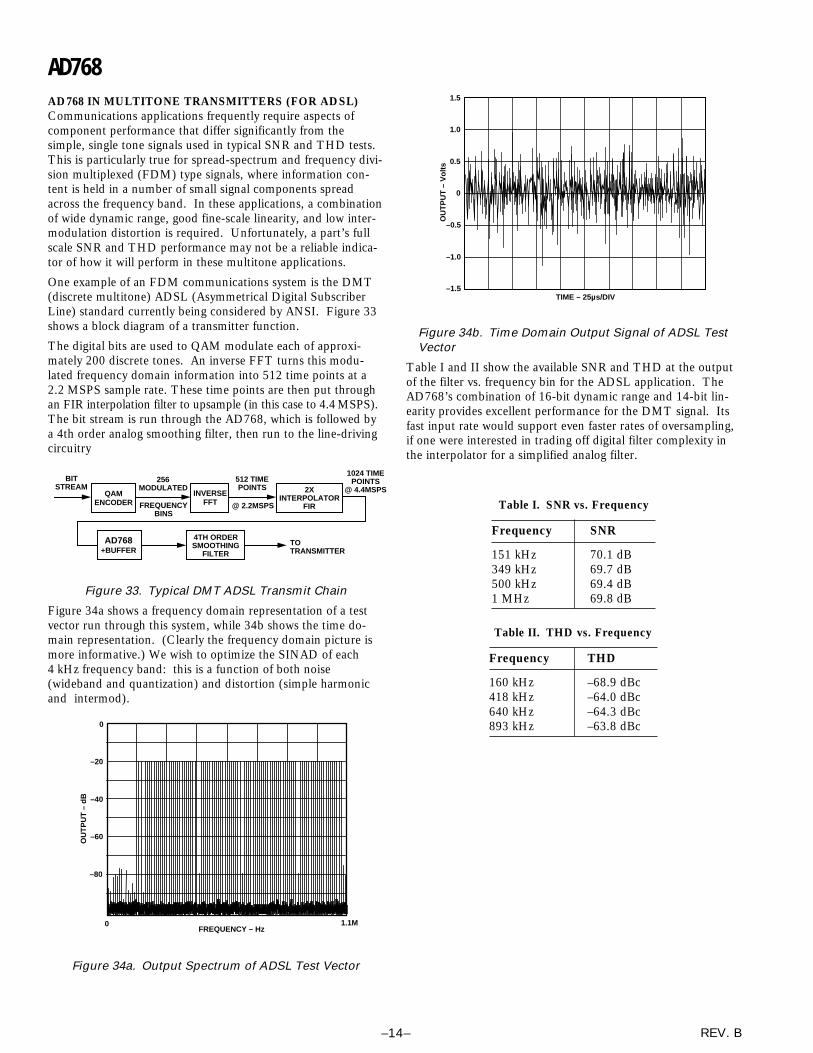
Figure 34a shows a frequency domain representation of a testvector run through this system, while 34b shows the time do-main representation. (Clearly the frequency domain picture ismore informative.) We wish to optimize the SINAD of each4 kHz frequency band: this is a function of both noise(wideband and quantization) and distortion (simple harmonicand intermod).
OU
TP
UT
– d
B
FREQUENCY – Hz
0
–20
–40
–60
0 1.1M
–80
Figure 34a. Output Spectrum of ADSL Test Vector
TIME – 25µs/DIV
1.5
1.0
0.5
0
–0.5
–1.0
–1.5
OU
TP
UT
– V
olt
s
Figure 34b. Time Domain Output Signal of ADSL TestVector
Table I and II show the available SNR and THD at the outputof the filter vs. frequency bin for the ADSL application. TheAD768’s combination of 16-bit dynamic range and 14-bit lin-earity provides excellent performance for the DMT signal. Itsfast input rate would support even faster rates of oversampling,if one were interested in trading off digital filter complexity inthe interpolator for a simplified analog filter.
Table I. SNR vs. Frequency
Frequency SNR
151 kHz 70.1 dB349 kHz 69.7 dB500 kHz 69.4 dB1 MHz 69.8 dB
Table II. THD vs. Frequency
Frequency THD
160 kHz –68.9 dBc418 kHz –64.0 dBc640 kHz –64.3 dBc893 kHz –63.8 dBc
AD768
REV. B –15–
AD768 EVALUATION BOARDGENERAL DESCRIPTIONThe AD768-EB is an evaluation board for the AD768 16-bit 30 Msps D/A converter. Careful attention to layout and circuitdesign combined with analog and digital prototyping areas al-lows the user to easily and effectively evaluate the AD768 in anyapplication where high resolution, high speed conversion isrequired.
The digital inputs to the AD768-EB may be driven directly us-ing the standard 40-pin IDC connector. An external clock isalso required. These signals may be applied from a user’sbench, or they can be generated from a circuit built on theprototyping area. The analog outputs from the AD768-EB areavailable on BNC connectors. These outputs may be configuredto use either resistors, op amps, or a transformer.
OPERATING PROCEDURE AND FUNCTIONALDESCRIPTIONPowerPower may be supplied to the AD768-EB by applying eitherwires or banana plugs to the metal binding posts included on theprinted circuit board.
DGND. Digital Ground. The digital ground and the analogground are connected together underneath the AD768. Optimalperformance can be obtained with separate analog and digitalsupplies. For evaluation purposes, a single-supply which makesa second analog and digital ground connection at the supply isacceptable.
+5D. The +5 V (±5%) digital supply should be capable of sup-plying 50 mA.
–5A. The –5 V (±5%) analog supply should be capable of sup-plying –75 mA.
AGND. Analog ground. The analog ground and the digitalground are connected together underneath the AD768. Optimalperformance can be obtained with separate analog and digitalsupplies. For evaluation purposes, a single-supply which makesa second analog and digital ground connection at the supply isacceptable.
–VEE. Negative analog supply; typically –5 V to –15 V. Thissupply is used as the negative supply rail for the external opamps. For the AD811 supplied with the AD768-EB, a supplycapable of supplying –20 mA (excluding external load require-ments) is required.
+VCC. Positive analog supply; typically +5 V to +15 V. Thissupply is used as the positive supply rail for the external opamps. For the AD811 supplied with the AD768-EB, a supplycapable of supplying +20 mA (excluding external load require-ments) is required.
Analog OutputsThe analog output(s) from the AD768-EB are available on BNCjacks “A” and “B.” The complementary current outputs fromthe AD768 can be configured using either resistors, op amps, ora transformer. Only the “A” portion of the AD768-EB is popu-lated and shipped from the factory. The “B” side, or comple-mentary output, may be populated by the user if so desired.
JP1. Buffered op amp output “A”. Jumper JP1 should beinstalled if the buffered op amp output is desired. When JP1is installed, JP2 and JP3 must be removed for properoperation. The output, available on the “A” connector, has anominal voltage swing of 0 V to 2 V and is in-phase with thedigital input. This is the factory default setting.
JP2. Bipolar 50 Ω transformer output. If jumper JP2 is in-stalled, a transformer coupled output is available on the “A”connector. When JP2 is installed, JP1 and JP3 must be re-moved for proper operation. The transformer acts both as adifferential-to-single-ended converter and as an impedancetransformer. For proper operation, the transformer must beterminated with a 50 Ω resistor. R2 must be replaced withthe 100 Ω resistor, R7. An additional 100 Ω resistor and thetransformer are included with the AD768-EB. The additional100 Ω resistor must be soldered into the appropriate position la-beled “R3” and the transformer must be inserted into thesocket labeled “T1.” The nominal output voltage into a 50 Ωload is 1 V p-p centered on a common-mode voltage of 0 V.
JP3. Resistor output “A.” JP3 is used to connect the resistorR2 to the “A” output. U2 should be removed from its socket.Using a 24.9 Ω resistor for R2, the output is an unbuffered 0 Vto –0.5 V output that is out of phase with the digital input. Re-sistor R2 may be replaced with other values, but careful atten-tion to the recommended output compliance range should beobserved. When JP3 is installed, JP1 and JP2 must be re-moved for proper operation.
JP4. Resistor output “B.” JP4 is used to connect the resistorR3 to the “A” output. U3 should be removed from its socket.The AD768-EB is shipped from the factory with resistor R3shorted to ground. A different value selected by the user can beinstalled for R3 to generate an unbuffered output that is in-phase with the digital input. Careful attention to the recom-mended output compliance range should be observed whenselecting the value of R3. When JP4 is installed, JP5 mustbe removed for proper operation.
JP5. Buffered op amp output “B.” Jumper JP5 should be in-stalled if the buffered op amp output is desired. When JP5 isinstalled, JP4 must be removed for proper operation.The output is available on the “B” connector and has a nominalvoltage swing determined by the combination of resistors R3,R9, and R10. This op amp is not provided with the AD768-EB.
ReferenceEither the internal reference of the AD768 or an external refer-ence may be selected on the AD768-EB. R12 is used to adjustthe full-scale output current of the AD768.
SW2. Internal/External reference select switch. When SW2 isin position 1, the internal reference of the AD768 is selected.When SW2 is in position 2, an external reference must be pro-vided by the user.
Level-Shifting the Analog OutputResistor sockets R8 and R6 can be populated with an appropri-ately valued resistor to add dc offset current to an output whichuses the op amp configuration. As an example, to generate abipolar output signal, a 1.25 kΩ resistor installed into the “R8”socket level-shifts the normally unipolar output by –1 V. Thefactory defaults for R8 and R6 are open circuits.
REV. B–16–
AD768Table III. Summary of Jumper Functionality
Installed Jumper Function
JumperJP1 Buffered Output AJP2 50 Ω Transformer OutputJP3 (STBY) Unbuffered Output AJP4 Unbuffered Output BJP5 Buffered Output B
Table IV. AD768-EB Parts List
Reference Value / Part Type Package Qty/Bd
U1 AD768 28-Pin SOIC 1
U2 AD811 8-Pin DIP 1
T1 Mini-Circuits Not Installed 1T4–6T
A, B, CLOCK BNC JACKs, Small, Vertical 3Small
JP1–5 Header 2-Pin 5
SW1, 2 SPDT, Secme 0.1" × 0.3" 2
J1 40-Pin IDC R.A., Male, 1Connector w/ Latches
R1 500 Ω 1/4 W, 0.01%, 1Vishay
R2 25 Ω 1/4 W, 0.01%, 1Vishay
R3, R13–21, &R23–29 Wire Jumpers 17
R5 500 Ω 1/4 W, 0.01%, 1Vishay
R7 100 Ω 1/4 W, 0.01%, 1Vishay
R11 51 Ω 1/8 W, 5%, Carbon 1
R12 10 kΩ Pot. 3266 W 1
C1–4 1 µF Ceram. Cap. Leaded 4
C5–8, C10, 12, 0.1 µF Chip Cap, 14, & C16–19 1206 11
C9, 11, 13, 15 22 µF Tant. Cap., Teardrop, 425 V 0.1" Spacing
Clock InputAn external sample clock must be provided to either the BNCconnector labeled “CLOCK” or on Pin 33 of the IDC connec-tor. This clock must comply with the logic levels outlined in theAD768 data sheet. The “CLOCK” input is terminated with aremovable 51 Ω resistor. The IDC connector clock connectionis unterminated.
SW1. Clock source select switch. When SW1 is in position 1, Pin33 of the IDC connected is applied to the CLOCK input of theAD768. When SW2 is in position 2, the “CLOCK” BNC connec-tor is applied to the CLOCK input of the AD768.
Digital InputsThe digital inputs of the AD768, DB0–DB15, are available viaJ1, a 40-pin IDC connector. These inputs should comply withthe specifications given in the AD768 data sheet.
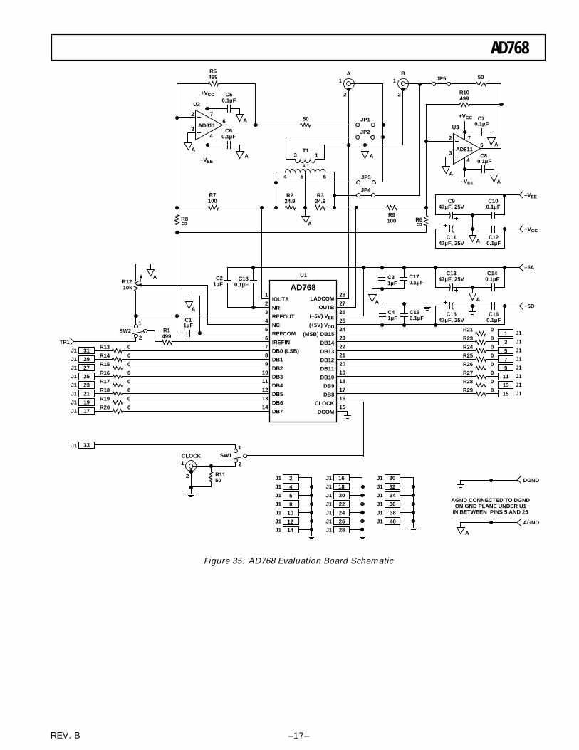
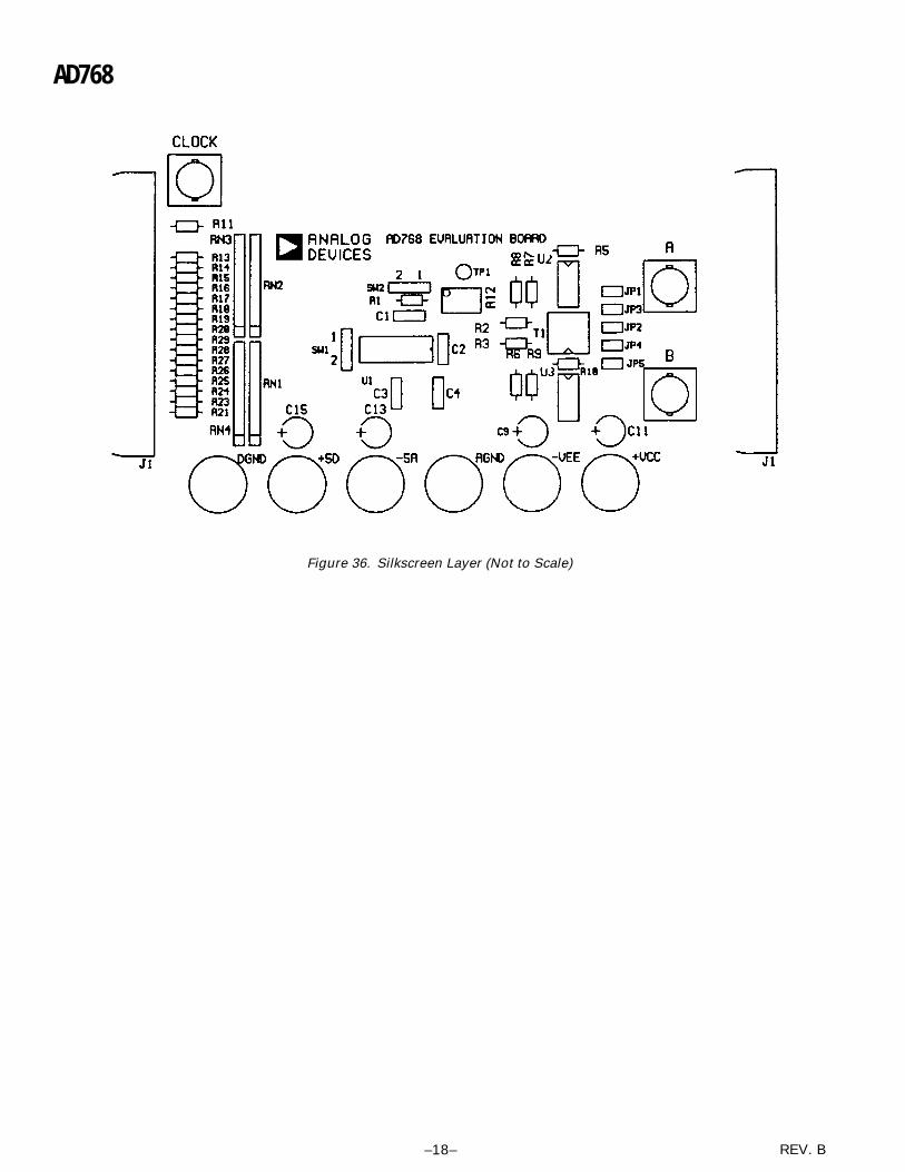
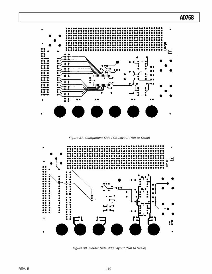
Layout ConsiderationsFigures 28 and 29 show the AD768-EB ground and powerplane layouts. Figures 35–38 show the schematic diagram, tracerouting, silk screening, and component layout for the AD768 4layer evaluation board.
Separate ground and power planes have several advantages forhigh speed layouts. (For further information outlining theseadvantages, see the application note “Design and Layout of aVideo Graphics System for Reduced EMI” [E1309] availablefrom Analog Devices [(617) 461-3392].) A solid ground planecan be used if the digital return current can be routed such thatit does not modulate the analog ground plane. If this is not pos-sible, it may be necessary to split the ground plane in order toforce currents to flow in a controlled direction. This type ofgrounding scheme is shown in the Figure 28. The ground planeis separated into analog and digital planes that are joinedtogether under the AD768. In any case, the AD768 should betreated as an analog component and a common ground connec-tion should be made underneath the AD768 despite some pinsbeing labeled “digital” ground and some as “analog” ground.
A complete parts list for the AD768 evaluation board is given inTable IV.
AD768
REV. B –17–
IOUTA
NR
REFOUT
NC
REFCOM
IREFIN
DB0 (LSB)
DB1
DB2
DB3
DB4
DB5
DB6
DB7
LADCOM
IOUTB
(–5V) VEE
(+5V) VDD
(MSB) DB15
DB14
DB13
DB12
DB11
DB10
DB9
DB8
CLOCK
DCOM
AD7681
2
3
4
5
6
7
8
9
10
11
12
13
14
28
27
26
25
24
23
22
21
20
19
18
17
16
15
C180.1µF
C21µF
C11µF
R1499
A
AR1210k
31
29
27
25
23
21
19
17
R13
R14
R15
R16
R17
R18
R19
R20
0
0
0
0
0
0
0
0
TP1
J1
J1
J1
J1
J1
J1
J1
J1
1
2SW2
C41µF
C190.1µF
C31µF
C170.1µF
A
C1547µF, 25V
C160.1µF
C1347µF, 25V
C140.1µF
A
R21
R23
R24
R25
R26
R27
R28
R29
0
0
0
0
0
0
0
0
1
3
5
7
9
11
13
15
J1
J1
J1
J1
J1
J1
J1
J1
–5A
+5D
33J1
CLOCK1
2
1
2
SW1
2
4
6
8
10
12
14
J1
J1
J1
J1
J1
J1
J1
16
18
20
22
24
26
28
J1
J1
J1
J1
J1
J1
J1
30
32
34
36
38
40
J1
J1
J1
J1
J1
J1
AGND CONNECTED TO DGNDON GND PLANE UNDER U1
IN BETWEEN PINS 5 AND 25
DGND
AGND
A
C1147µF, 25V
C120.1µF
C947µF, 25V
C100.1µF
A
–VEE
+VCC
A
C70.1µF
+VCC
–VEE
A
AD811
76
2
34
U3
U1
R10499
50JP5
R6∞
C50.1µF
A
+VCC
–VEE
A
AD811
76
2
34
U2
R5499
C60.1µF
A
C80.1µF
A B11
2 2
JP1
JP2
50
4:1
3 1T1
4 5 6 JP3
JP4
R9100
R324.9
R224.9
R8∞ A
R7100
R1150
A A
Figure 35. AD768 Evaluation Board Schematic
REV. B–18–
AD768
Figure 36. Silkscreen Layer (Not to Scale)
AD768
REV. B –19–
Figure 37. Component Side PCB Layout (Not to Scale)
Figure 38. Solder Side PCB Layout (Not to Scale)
REV. B–20–
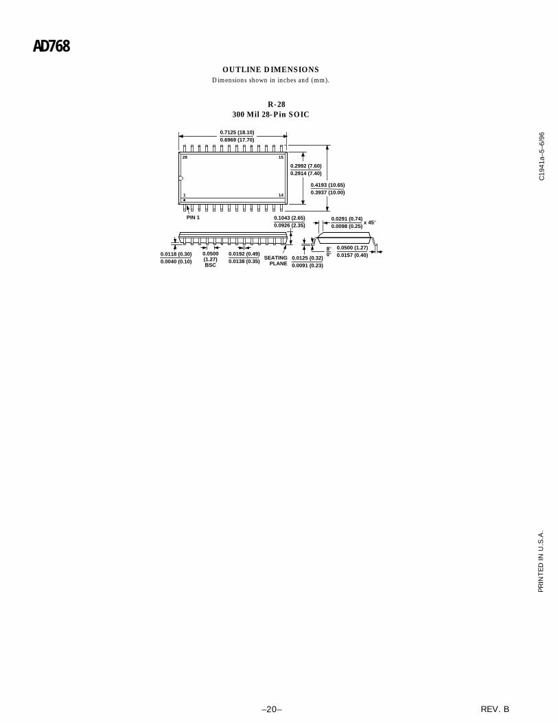
AD768OUTLINE DIMENSIONS
Dimensions shown in inches and (mm).
R-28300 Mil 28-Pin SOIC
SEATINGPLANE
0.0118 (0.30)0.0040 (0.10)
0.0192 (0.49)0.0138 (0.35)
0.1043 (2.65)0.0926 (2.35)
0.0500(1.27)BSC
0.0125 (0.32)0.0091 (0.23)
0.0500 (1.27)0.0157 (0.40)
8°0°
0.0291 (0.74)0.0098 (0.25)
x 45°
0.7125 (18.10)0.6969 (17.70)
0.4193 (10.65)0.3937 (10.00)
0.2992 (7.60)0.2914 (7.40)
PIN 1
28 15
141
PR
INT
ED
IN U
.S.A
.C
1941
a–5–
6/96

Mouser Electronics
Authorized Distributor
Click to View Pricing, Inventory, Delivery & Lifecycle Information: Analog Devices Inc.:
AD768ARZ AD768AR AD768ARZ-REEL