Embed Size (px)
Citation preview
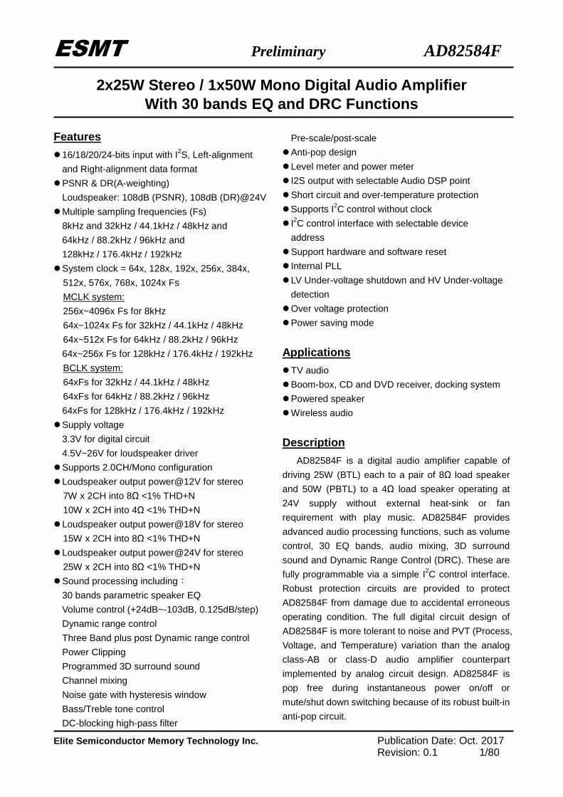
ESMT Preliminary AD82584F
Elite Semiconductor Memory Technology Inc. Publication Date: Oct. 2017 Revision: 0.1 1/80
2x25W Stereo / 1x50W Mono Digital Audio Amplifier With 30 bands EQ and DRC Functions
Features
16/18/20/24-bits input with I2S, Left-alignment
and Right-alignment data format
PSNR & DR(A-weighting)
Loudspeaker: 108dB (PSNR), 108dB (DR)@24V
Multiple sampling frequencies (Fs)
8kHz and 32kHz / 44.1kHz / 48kHz and
64kHz / 88.2kHz / 96kHz and
128kHz / 176.4kHz / 192kHz
System clock = 64x, 128x, 192x, 256x, 384x,
512x, 576x, 768x, 1024x Fs
MCLK system:
256x~4096x Fs for 8kHz
64x~1024x Fs for 32kHz / 44.1kHz / 48kHz
64x~512x Fs for 64kHz / 88.2kHz / 96kHz
64x~256x Fs for 128kHz / 176.4kHz / 192kHz
BCLK system:
64xFs for 32kHz / 44.1kHz / 48kHz
64xFs for 64kHz / 88.2kHz / 96kHz
64xFs for 128kHz / 176.4kHz / 192kHz
Supply voltage
3.3V for digital circuit
4.5V~26V for loudspeaker driver
Supports 2.0CH/Mono configuration
Loudspeaker output power@12V for stereo
7W x 2CH into 8Ω <1% THD+N
10W x 2CH into 4Ω <1% THD+N
Loudspeaker output power@18V for stereo
15W x 2CH into 8Ω <1% THD+N
Loudspeaker output power@24V for stereo
25W x 2CH into 8Ω <1% THD+N
Sound processing including:
30 bands parametric speaker EQ
Volume control (+24dB~-103dB, 0.125dB/step)
Dynamic range control
Three Band plus post Dynamic range control
Power Clipping
Programmed 3D surround sound
Channel mixing
Noise gate with hysteresis window
Bass/Treble tone control
DC-blocking high-pass filter
Pre-scale/post-scale
Anti-pop design
Level meter and power meter
I2S output with selectable Audio DSP point
Short circuit and over-temperature protection
Supports I2C control without clock
I2C control interface with selectable device
address
Support hardware and software reset
Internal PLL
LV Under-voltage shutdown and HV Under-voltage
detection
Over voltage protection
Power saving mode Applications
TV audio
Boom-box, CD and DVD receiver, docking system
Powered speaker
Wireless audio Description
AD82584F is a digital audio amplifier capable of
driving 25W (BTL) each to a pair of 8Ω load speaker
and 50W (PBTL) to a 4Ω load speaker operating at
24V supply without external heat-sink or fan
requirement with play music. AD82584F provides
advanced audio processing functions, such as volume
control, 30 EQ bands, audio mixing, 3D surround
sound and Dynamic Range Control (DRC). These are
fully programmable via a simple I2C control interface.
Robust protection circuits are provided to protect
AD82584F from damage due to accidental erroneous
operating condition. The full digital circuit design of
AD82584F is more tolerant to noise and PVT (Process,
Voltage, and Temperature) variation than the analog
class-AB or class-D audio amplifier counterpart
implemented by analog circuit design. AD82584F is
pop free during instantaneous power on/off or
mute/shut down switching because of its robust built-in
anti-pop circuit.
ESMT Preliminary AD82584F
Elite Semiconductor Memory Technology Inc. Publication Date: Oct. 2017 Revision: 0.1 2/80
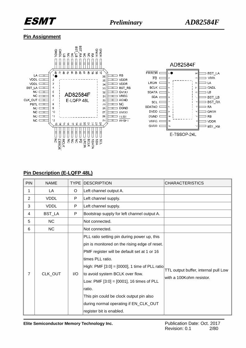
Pin Assignment
Pin Description (E-LQFP 48L)
PIN NAME TYPE DESCRIPTION CHARACTERISTICS
1 LA O Left channel output A.
2 VDDL P Left channel supply.
3 VDDL P Left channel supply.
4 BST_LA P Bootstrap supply for left channel output A.
5 NC Not connected.
6 NC Not connected.
7 CLK_OUT I/O
PLL ratio setting pin during power up, this
pin is monitored on the rising edge of reset.
PMF register will be default set at 1 or 16
times PLL ratio.
High: PMF [3:0] = [0000], 1 time of PLL ratio
to avoid system BCLK over flow.
Low: PMF [3:0] = [0001], 16 times of PLL
ratio.
This pin could be clock output pin also
during normal operating if EN_CLK_OUT
register bit is enabled.
TTL output buffer, internal pull Low
with a 100Kohm resistor.
ESMT Preliminary AD82584F
Elite Semiconductor Memory Technology Inc. Publication Date: Oct. 2017 Revision: 0.1 3/80
8 PBTL I Stereo/Mono configuration pin.
(Low: Stereo ; High: Mono)
9 NC Not connected.
10 NC Not connected.
11 NC Not connected.
12 NC Not connected.
13 NC Not connected.
14 ERROR I/O
ERROR pin is a dual function pin. One is I2C
address setting during power up. The other
one is error status report (low active), It sets
by register of A_SEL_FAULT at address
0x1C B[6] to enable it.
This pin is monitored on the rising
edge of reset. A value of Low (15-kΩ
pull down) sets the I2C device
address to 0x30 and a value of High
(15-kΩ pull up) sets it to 0x31.
15 MCLK I Master clock input.
Schmitt trigger TTL input buffer,
internal pull Low with a 80Kohm
resistor.
16 NC Not connected.
17 NC Not connected.
18 NC Not connected.
19 PD I Power down, low active.
Schmitt trigger TTL input buffer,
internal pull High with a 330Kohm
resistor.
20 LRCIN I Left/Right clock input (Fs).
Schmitt trigger TTL input buffer,
internal pull Low with an 80Kohm
resistor.
21 BCLK I Bit clock input (64Fs).
Schmitt trigger TTL input buffer,
internal pull Low with an 80Kohm
resistor.
22 SDATA I Serial audio data input. Schmitt trigger TTL input buffer
23 SDA I/O I2C bi-directional serial data. Schmitt trigger TTL input buffer
24 SCL I I2C serial clock input. Schmitt trigger TTL input buffer
25 RESET I Reset, low active.
Schmitt trigger TTL input buffer,
internal pull High with a 330Kohm
resistor.
26 TEST I This pin must connect to GND.
27 DVDD P Digital Power.
28 DGND P Digital Ground.
29 NC Not connected.
ESMT Preliminary AD82584F
Elite Semiconductor Memory Technology Inc. Publication Date: Oct. 2017 Revision: 0.1 4/80
30 AGND P Analog Ground.
31 VREG O 1.8V Regulator voltage output.
32 GVDD O 5V Regulator voltage output. This pin must
not be used to drive external devices.
33 BST_RB P Bootstrap supply for right channel output B.
34 VDDR P Right channel supply.
35 VDDR P Right channel supply.
36 RB O Right channel output B.
37 GNDR P Right channel ground.
38 GNDR P Right channel ground.
39 RA O Right channel output A.
40 NC Not connected.
41 NC Not connected.
42 BST_RA P Bootstrap supply for right channel output A.
43 BST_LB P Bootstrap supply for left channel output B.
44 NC Not connected.
45 NC Not connected.
46 LB O Left channel output B.
47 GNDL P Left channel ground.
48 GNDL P Left channel ground.
ESMT Preliminary AD82584F
Elite Semiconductor Memory Technology Inc. Publication Date: Oct. 2017 Revision: 0.1 5/80
Pin Description (E-TSSOP 24L)
PIN NAME TYPE DESCRIPTION CHARACTERISTICS
1 ERROR I/O
ERROR pin is a dual function pin. One is I2C
address setting during power up. The other
one is error status report (low active), It sets
by register of A_SEL_FAULT at address
0x1C B[6] to enable it.
This pin is monitored on the rising
edge of reset. A value of Low (15-kΩ
pull down) sets the I2C device
address to 0x30 and a value of High
(15-kΩ pull up) sets it to 0x31.
2 PD I Power down, low active.
Schmitt trigger TTL input buffer,
internal pull High with a 330Kohm
resistor.
3 LRCIN I Left/Right clock input (Fs).
Schmitt trigger TTL input buffer,
internal pull Low with an 80Kohm
resistor.
4 BCLK I Bit clock input (64Fs).
Schmitt trigger TTL input buffer,
internal pull Low with an 80Kohm
resistor.
5 SDATA I Serial audio data input. Schmitt trigger TTL input buffer
6 SDA I/O I2C bi-directional serial data. Schmitt trigger TTL input buffer
7 SCL I I2C serial clock input. Schmitt trigger TTL input buffer
8 SDATAO O Serial audio data output. Schmitt trigger TTL input buffer
9 DVDD P Digital Power.
10 DGND P Digital Ground.
11 VREG O 1.8V Regulator voltage output.
12 GVDD O 5V Regulator voltage output. This pin must
not be used to drive external devices.
13 BST_RB P Bootstrap supply for right channel output B.
14 VDDR P Right channel supply.
15 RB O Right channel output B.
16 GNDR P Right channel ground.
17 RA O Right channel output A.
18 BST_RA P Bootstrap supply for right channel output A.
19 BST_LB P Bootstrap supply for left channel output B.
20 LB O Left channel output B.
21 GNDL P Left channel ground.
22 LA O Left channel output A.
23 VDDL P Left channel supply.
24 BST_LA P Bootstrap supply for left channel output A.
ESMT Preliminary AD82584F
Elite Semiconductor Memory Technology Inc. Publication Date: Oct. 2017 Revision: 0.1 6/80
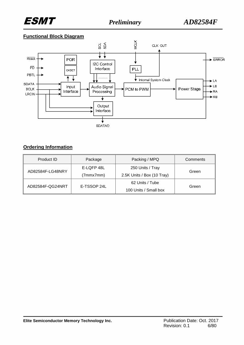
Functional Block Diagram
Ordering Information
Product ID Package Packing / MPQ Comments
AD82584F-LG48NRY E-LQFP 48L
(7mmx7mm)
250 Units / Tray
2.5K Units / Box (10 Tray) Green
AD82584F-QG24NRT E-TSSOP 24L 62 Units / Tube
100 Units / Small box Green
ESMT Preliminary AD82584F
Elite Semiconductor Memory Technology Inc. Publication Date: Oct. 2017 Revision: 0.1 7/80
Available Package
Package Type Device No. θja(/W) Ψjt(/W) θjt(/W) Exposed Thermal Pad
E-LQFP 48L AD82584F
22.9 1.64 34.9 Yes (Note1)
E-TSSOP 24L 26.8 1.83 27.1
Note 1.1: The thermal pad is located at the bottom of the package. To optimize thermal performance, soldering the thermal pad to the PCB’s ground plane is suggested.
Note 1.2: θja, the junction-to-ambient thermal resistance is simulated on a room temperature (TA=25), natural convection environment test board, which is constructed with a thermally efficient, 4-layers PCB (2S2P). The simulation is tested using the JESD51-5 thermal measurement standard.
Note 1.3: Ψjt represents the thermal parameter for the heat flow between the chip junction and the package’s top surface center. It’s extracted from the simulation data for obtainingθja, using a procedure described in JESD51-2.
Note 1.4: θjt represents the thermal resistance for the heat flow between the chip junction and the package’s
top surface. It’s extracted from the simulation data with obtaining a cold plate on the package top.
Marking Information
AD82584F
Line 1 : LOGO
Line 2 : Product no.
Line 3 : Tracking Code
Line 4 : Date Code
Absolute Maximum Ratings
Stresses beyond those listed under absolute maximum ratings may cause permanent damage to the device.
Symbol Parameter Min Max Units
DVDD Supply for Digital Circuit -0.3 3.6 V
VDDL/R Supply for Driver Stage -0.3 30 V
Vi Input Voltage -0.3 3.6 V
Tstg Storage Temperature -65 150 oC
TJ Junction Operating Temperature 0 150 oC
E-LQFP 48L E-TSSOP 24L
ESMT Preliminary AD82584F
Elite Semiconductor Memory Technology Inc. Publication Date: Oct. 2017 Revision: 0.1 8/80
Recommended Operating Conditions
General Electrical Characteristics
Condition: TA=25 oC (unless otherwise specified).
Symbol Parameter Condition Min Typ Max Units
IPD(HV) PVDD Supply Current during Power Down PVDD=24V 20 40 uA
IQ(HV) Quiescent current for PVDD
(50%/50% PWM duty) PVDD=24V 15 mA
IQ(LV) Quiescent current for DVDD (Un-mute) DVDD=3.3V,
PBTL=Low 31 mA
TSENSOR Junction Temperature for Driver Shutdown 165 oC
Temperature Hysteresis for Recovery from Shutdown 35 oC
UVDVDDH DVDD Under Voltage Release 2.99 V
UVDVDDL DVDD Under Voltage Active 2.89 V
UVPVDDH VDDL/R Under Voltage Release 7.7 V
UVPVDDL VDDL/R Under Voltage Active 7.1 V
OVH VDDL/R Over Voltage Active 29.2 V
OVL VDDL/R Under Voltage Release 28.5 V
Static Drain-to-Source On-state Resistor, NMOS PVDD=24V, Id=500mA 180 mΩ
ISC
L(R) Channel Over-Current Protection (Note 2) PVDD=24V 9 A
PVDD=12V 8.5 A
Mono Over-Current Protection (Note 2) PVDD=24V 18 A
PVDD=12V 17 A
VIH High-Level Input Voltage DVDD=3.3V 2.0 V
VIL Low-Level Input Voltage DVDD=3.3V 0.8 V
VOH High-Level Output Voltage DVDD=3.3V 2.4 V
VOL Low-Level Output Voltage DVDD=3.3V 0.4 V
CI Input Capacitance 6.4 pF
Note 2: Loudspeaker over-current protection is only effective when loudspeaker drivers are properly connected with external LC filters. Please refer to the application circuit example for recommended LC filter configuration.
Symbol Parameter Typ Units
DVDD Supply for Digital Circuit 3.15~3.45 V
VDDL/R Supply for Driver Stage 4.5~26 V
TJ Junction Operating Temperature -40~125 oC
TA Ambient Operating Temperature -40~85 oC
ESMT Preliminary AD82584F
Elite Semiconductor Memory Technology Inc. Publication Date: Oct. 2017 Revision: 0.1 9/80
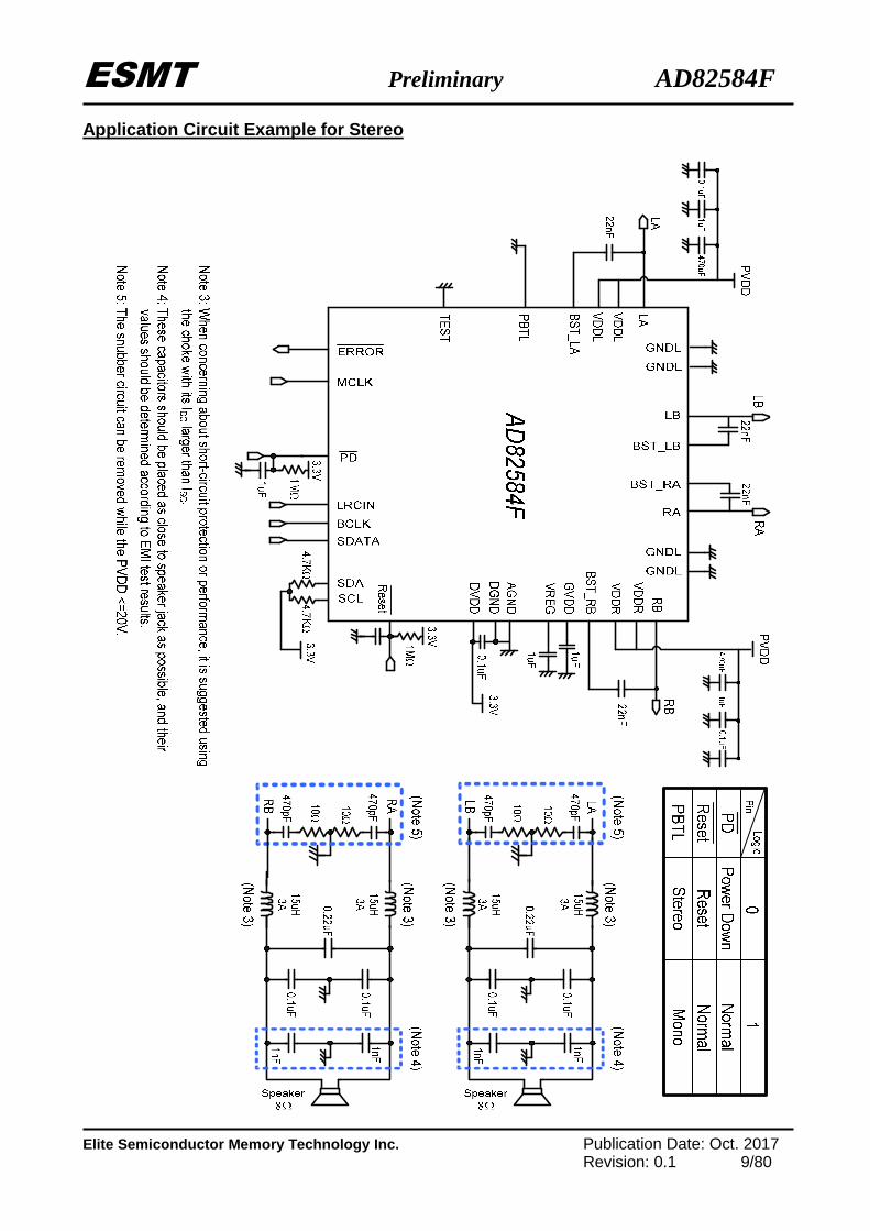
Application Circuit Example for Stereo
ESMT Preliminary AD82584F
Elite Semiconductor Memory Technology Inc. Publication Date: Oct. 2017 Revision: 0.1 10/80
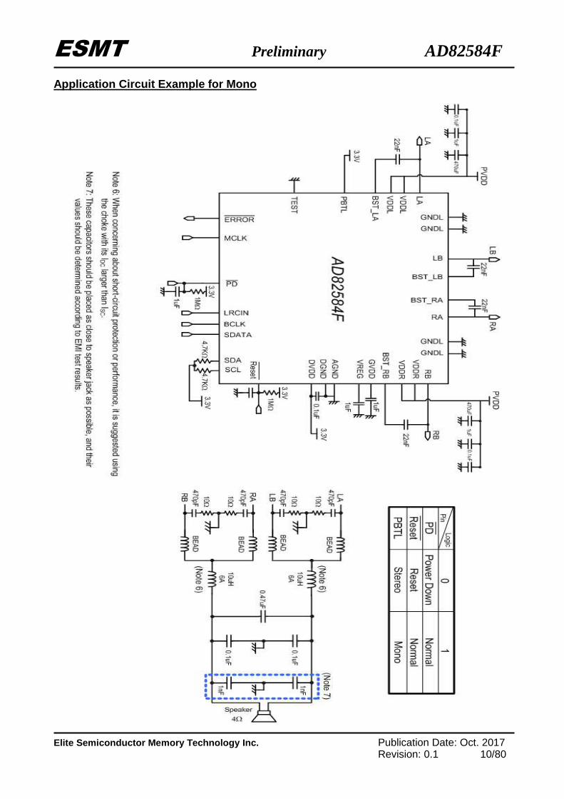
Application Circuit Example for Mono
ESMT Preliminary AD82584F
Elite Semiconductor Memory Technology Inc. Publication Date: Oct. 2017 Revision: 0.1 11/80
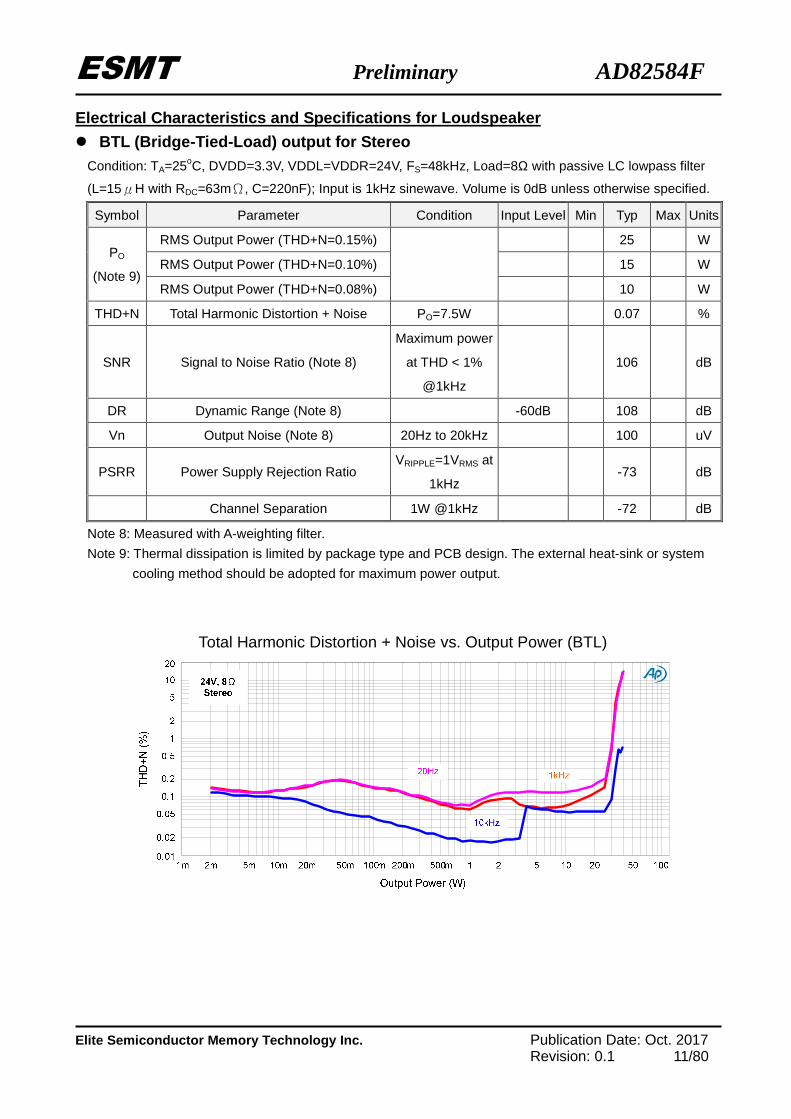
Electrical Characteristics and Specifications for Loudspeaker
BTL (Bridge-Tied-Load) output for Stereo Condition: TA=25oC, DVDD=3.3V, VDDL=VDDR=24V, FS=48kHz, Load=8Ω with passive LC lowpass filter
(L=15μH with RDC=63mΩ, C=220nF); Input is 1kHz sinewave. Volume is 0dB unless otherwise specified.
Symbol Parameter Condition Input Level Min Typ Max Units
PO
(Note 9)
RMS Output Power (THD+N=0.15%)
25 W
RMS Output Power (THD+N=0.10%) 15 W
RMS Output Power (THD+N=0.08%) 10 W
THD+N Total Harmonic Distortion + Noise PO=7.5W 0.07 %
SNR Signal to Noise Ratio (Note 8)
Maximum power
at THD < 1%
@1kHz
106 dB
DR Dynamic Range (Note 8) -60dB 108 dB
Vn Output Noise (Note 8) 20Hz to 20kHz 100 uV
PSRR Power Supply Rejection Ratio VRIPPLE=1VRMS at
1kHz -73 dB
Channel Separation 1W @1kHz -72 dB
Note 8: Measured with A-weighting filter.
Note 9: Thermal dissipation is limited by package type and PCB design. The external heat-sink or system
cooling method should be adopted for maximum power output.
Total Harmonic Distortion + Noise vs. Output Power (BTL)
ESMT Preliminary AD82584F
Elite Semiconductor Memory Technology Inc. Publication Date: Oct. 2017 Revision: 0.1 12/80
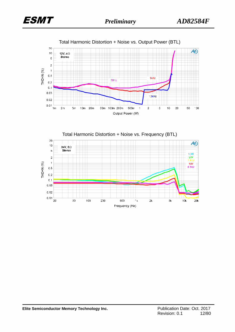
Total Harmonic Distortion + Noise vs. Output Power (BTL)
Total Harmonic Distortion + Noise vs. Frequency (BTL)
ESMT Preliminary AD82584F
Elite Semiconductor Memory Technology Inc. Publication Date: Oct. 2017 Revision: 0.1 13/80
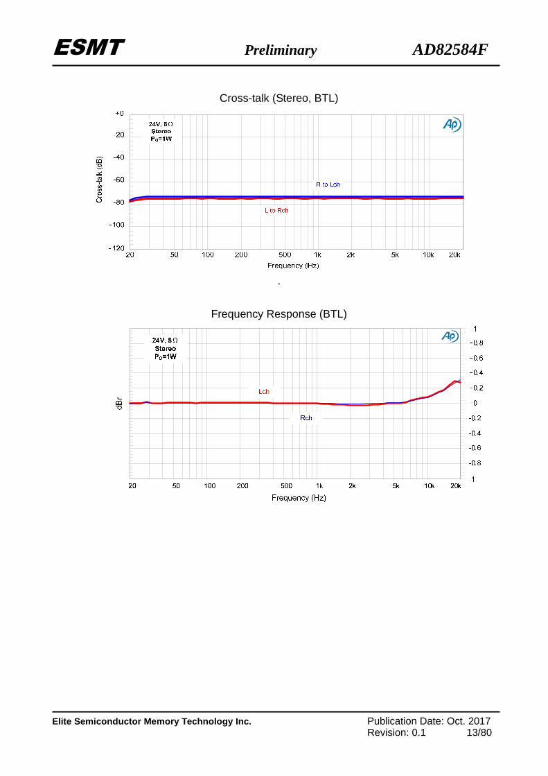
Cross-talk (Stereo, BTL)
.
Frequency Response (BTL)
ESMT Preliminary AD82584F
Elite Semiconductor Memory Technology Inc. Publication Date: Oct. 2017 Revision: 0.1 14/80
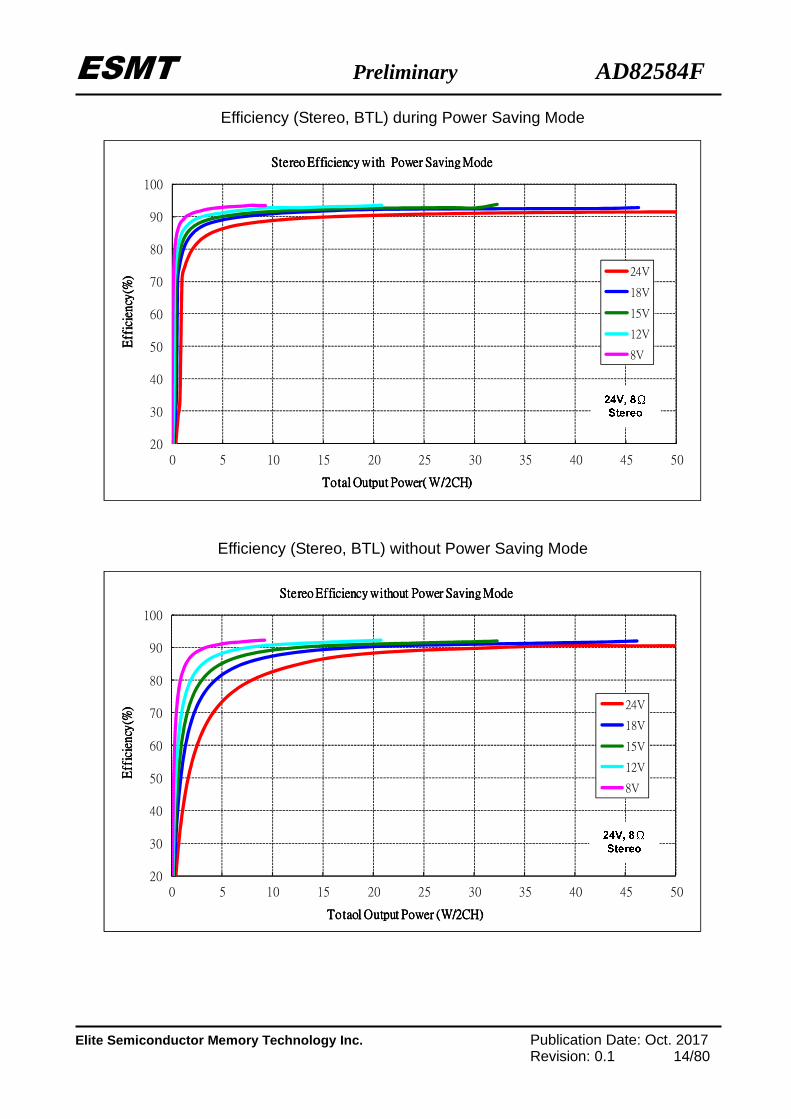
Efficiency (Stereo, BTL) during Power Saving Mode
20
30
40
50
60
70
80
90
100
0 5 10 15 20 25 30 35 40 45 50
Eff
icie
ncy(
%)
Eff
icie
ncy(
%)
Eff
icie
ncy(
%)
Eff
icie
ncy(
%)
Total Output Power( W/Total Output Power( W/Total Output Power( W/Total Output Power( W/2222CH)CH)CH)CH)
Stereo Efficiency with Power Saving ModeStereo Efficiency with Power Saving ModeStereo Efficiency with Power Saving ModeStereo Efficiency with Power Saving Mode
24V
18V
15V
12V
8V
Efficiency (Stereo, BTL) without Power Saving Mode
20
30
40
50
60
70
80
90
100
0 5 10 15 20 25 30 35 40 45 50
Eff
icie
ncy(
%)
Eff
icie
ncy(
%)
Eff
icie
ncy(
%)
Eff
icie
ncy(
%)
Totaol Output Power (W/Totaol Output Power (W/Totaol Output Power (W/Totaol Output Power (W/2222CH)CH)CH)CH)
Stereo Efficiency without Power Saving ModeStereo Efficiency without Power Saving ModeStereo Efficiency without Power Saving ModeStereo Efficiency without Power Saving Mode
24V
18V
15V
12V
8V
ESMT Preliminary AD82584F
Elite Semiconductor Memory Technology Inc. Publication Date: Oct. 2017 Revision: 0.1 15/80
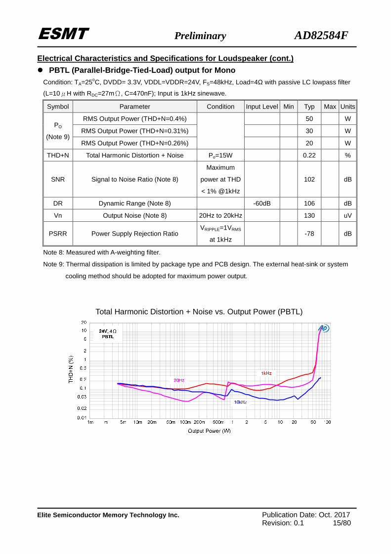
Electrical Characteristics and Specifications for Loudspeaker (cont.)
PBTL (Parallel-Bridge-Tied-Load) output for Mono Condition: TA=25oC, DVDD= 3.3V, VDDL=VDDR=24V, FS=48kHz, Load=4Ω with passive LC lowpass filter
(L=10μH with RDC=27mΩ, C=470nF); Input is 1kHz sinewave.
Symbol Parameter Condition Input Level Min Typ Max Units
PO
(Note 9)
RMS Output Power (THD+N=0.4%)
50 W
RMS Output Power (THD+N=0.31%) 30 W
RMS Output Power (THD+N=0.26%) 20 W
THD+N Total Harmonic Distortion + Noise Po=15W 0.22 %
SNR Signal to Noise Ratio (Note 8)
Maximum
power at THD
< 1% @1kHz
102 dB
DR Dynamic Range (Note 8) -60dB 106 dB
Vn Output Noise (Note 8) 20Hz to 20kHz 130 uV
PSRR Power Supply Rejection Ratio VRIPPLE=1VRMS
at 1kHz -78 dB
Note 8: Measured with A-weighting filter.
Note 9: Thermal dissipation is limited by package type and PCB design. The external heat-sink or system
cooling method should be adopted for maximum power output.
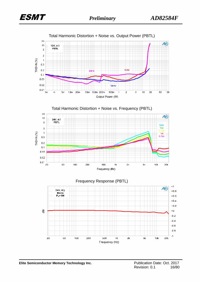
Total Harmonic Distortion + Noise vs. Output Power (PBTL)
ESMT Preliminary AD82584F
Elite Semiconductor Memory Technology Inc. Publication Date: Oct. 2017 Revision: 0.1 16/80
Total Harmonic Distortion + Noise vs. Output Power (PBTL)
Total Harmonic Distortion + Noise vs. Frequency (PBTL)
TH
D+
N (
%)
Frequency Response (PBTL)
ESMT Preliminary AD82584F
Elite Semiconductor Memory Technology Inc. Publication Date: Oct. 2017 Revision: 0.1 17/80
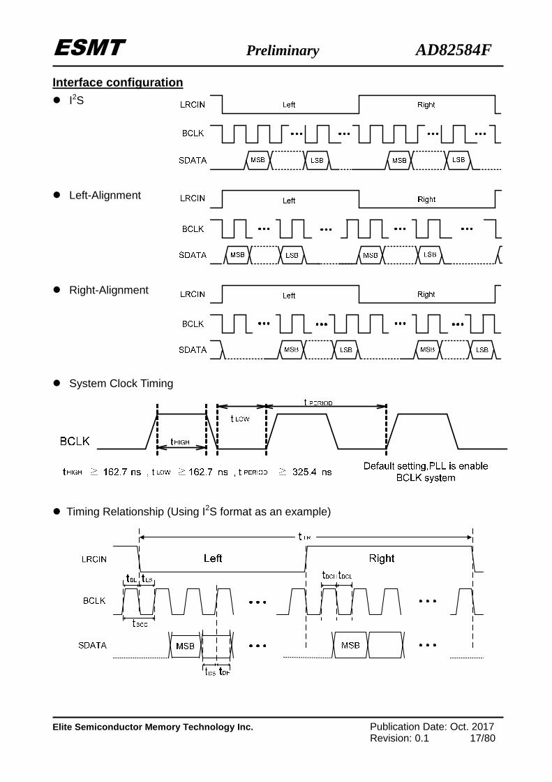
Interface configuration I2S
Left-Alignment
Right-Alignment
System Clock Timing
Timing Relationship (Using I2S format as an example)
ESMT Preliminary AD82584F
Elite Semiconductor Memory Technology Inc. Publication Date: Oct. 2017 Revision: 0.1 18/80
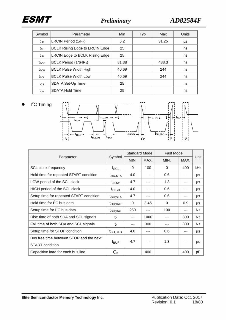
Symbol Parameter Min Typ Max Units
tLR LRCIN Period (1/FS) 5.2 31.25 µs
tBL BCLK Rising Edge to LRCIN Edge 25 ns
tLB LRCIN Edge to BCLK Rising Edge 25 ns
tBCC BCLK Period (1/64FS) 81.38 488.3 ns
tBCH BCLK Pulse Width High 40.69 244 ns
tBCL BCLK Pulse Width Low 40.69 244 ns
tDS SDATA Set-Up Time 25 ns
tDH SDATA Hold Time 25 ns
I2C Timing
Parameter Symbol Standard Mode Fast Mode
Unit MIN. MAX. MIN. MAX.
SCL clock frequency fSCL 0 100 0 400 kHz
Hold time for repeated START condition tHD,STA 4.0 --- 0.6 --- µs
LOW period of the SCL clock tLOW 4.7 --- 1.3 --- µs
HIGH period of the SCL clock tHIGH 4.0 --- 0.6 --- µs
Setup time for repeated START condition tSU;STA 4.7 --- 0.6 --- µs
Hold time for I2C bus data tHD;DAT 0 3.45 0 0.9 µs
Setup time for I2C bus data tSU;DAT 250 --- 100 --- Ns
Rise time of both SDA and SCL signals tr --- 1000 --- 300 Ns
Fall time of both SDA and SCL signals tf --- 300 --- 300 Ns
Setup time for STOP condition tSU;STO 4.0 --- 0.6 --- µs
Bus free time between STOP and the next
START condition tBUF 4.7 --- 1.3 --- µs
Capacitive load for each bus line Cb 400 400 pF
ESMT Preliminary AD82584F
Elite Semiconductor Memory Technology Inc. Publication Date: Oct. 2017 Revision: 0.1 19/80
Operation Description The default volume of AD82584F is muted. AD82584F will be activated while the de-mute command via I2C is
programmed.
Internal PLL AD82584F has a built-in PLL internally, the BCLK/FS or MCLK/FS ratio, which is selected by I2C control
interface. The clock inputted into the BCLK or MCLK pin becomes the frequency of multiple edge evaluation
in chip internally.
Fs BCLK/FS Setting
Ratio for PLL BCLK Frequency
Multiple edge
evaluation for bit
clock
PWM Career
Frequency
48kHz 64x 3.072MHz 32x 384kHz
44.1kHz 64x 2.8224MHz 32x 352.8kHz
32kHz 64x 2.048MHz 32x 256kHz
Fs MCLK/FS Setting
Ratio for PLL MCLK Frequency
Multiple edge
evaluation for
Master clock
PWM Career
Frequency
48kHz 256x 12.288MHz 8x 384kHz
44.1kHz 256x 11.2896MHz 8x 352.8kHz
32kHz 256x 8.192MHz 8x 256kHz
8kHz 256x 2.048MHz 32x 256kHz
Reset
When the RESET pin is lowered, AD82584F will clear the stored data and reset the register table to
default values. AD82584F will exit reset state at the 512th internal clock cycle after the RESET pin is
raised to high.
ESMT Preliminary AD82584F
Elite Semiconductor Memory Technology Inc. Publication Date: Oct. 2017 Revision: 0.1 20/80
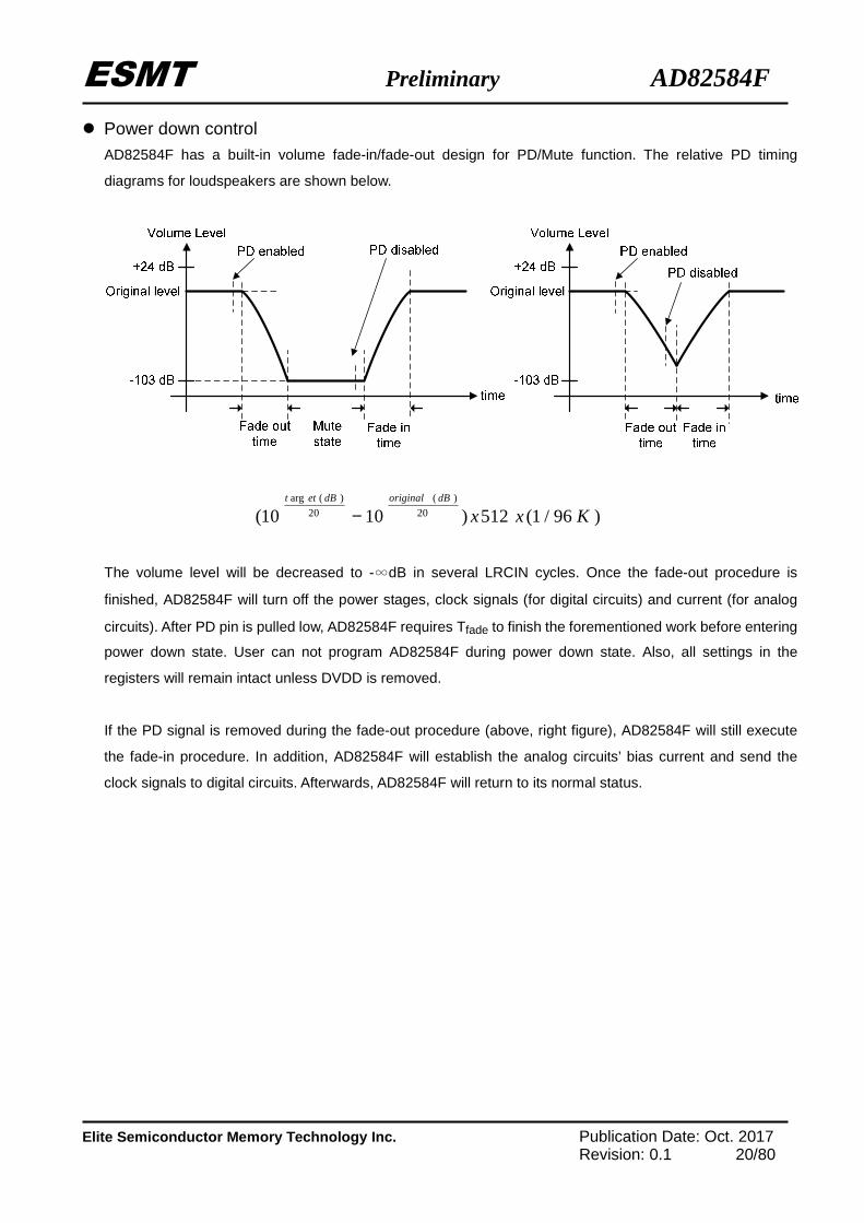
Power down control AD82584F has a built-in volume fade-in/fade-out design for PD/Mute function. The relative PD timing
diagrams for loudspeakers are shown below.
The volume level will be decreased to -∞dB in several LRCIN cycles. Once the fade-out procedure is
finished, AD82584F will turn off the power stages, clock signals (for digital circuits) and current (for analog
circuits). After PD pin is pulled low, AD82584F requires Tfade to finish the forementioned work before entering
power down state. User can not program AD82584F during power down state. Also, all settings in the
registers will remain intact unless DVDD is removed.
If the PD signal is removed during the fade-out procedure (above, right figure), AD82584F will still execute
the fade-in procedure. In addition, AD82584F will establish the analog circuits’ bias current and send the
clock signals to digital circuits. Afterwards, AD82584F will return to its normal status.
)96/1(512)1010( 20
)(
20
)(arg
KxxdBoriginaldBett
−
ESMT Preliminary AD82584F
Elite Semiconductor Memory Technology Inc. Publication Date: Oct. 2017 Revision: 0.1 21/80
Self-protection circuits AD82584F has built-in protection circuits including thermal, short-circuit, under-voltage detection, and over
voltage circuits.
(i) When the internal junction temperature is higher than 165, power stages will be turned off and
AD82584F will return to normal operation once the temperature drops to 130. The temperature values
may vary around 10%.
(ii) The short-circuit protection circuit protects the output stage when the wires connected to loudspeakers
are shorted to each other or GND/VDD. For normal 24V operations, the current flowing through the
power stage will be less than 9A for stereo configuration. Otherwise, the short-circuit detectors may pull
the ERROR pin to DGND, disabling the output stages. When the over-temperature or short-circuit
condition occurs, the open-drain ERROR pin will be pulled low and latched into ERROR state.
Once short-circuit condition is removed, AD82584F will exit ERROR state when one of the following
conditions is met: (1) RESET pin is pulled low, (2) PD pin is pulled low, (3) Master mute is enabled
through the I2C interface.
(iii) Once the DVDD voltage is lower than 2.89V, AD82584F will turn off its loudspeaker power stages. When
DVDD becomes higher than 2.99V, AD82584F will return to normal operation.
(iv) Once the PVDD voltage is higher than 29.2V, AD82584F will turn off its loudspeaker power stages.
When PVDD becomes lower than 28.5V, AD82584F will return to normal operation.
(v) Once the PVDD voltage is lower than 7.1V, AD82584F will turn off its loudspeaker power stages. When
PVDD becomes higher than 7.7V, AD82584F will return to normal operation.
Anti-pop design AD82584F will generate appropriate control signals to suppress pop sounds during initial power on/off,
power down/up, mute, and volume level changes.
3D surround sound AD82584F provides the virtual surround sound technology with greater separation and depth voice quality
for stereo signals.
I2C Chip Select
ERROR is an input pin during power. It can be pulled High (15-kΩ pull up) or Low (15-kΩ pull down). Low
indicates an I2C address of 0x30, and high an address of 0x31.
ESMT Preliminary AD82584F
Elite Semiconductor Memory Technology Inc. Publication Date: Oct. 2017 Revision: 0.1 22/80
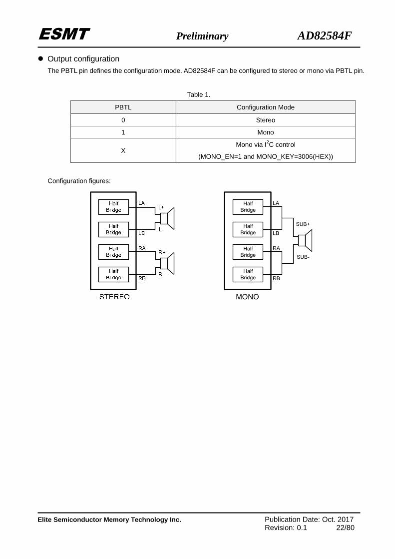
Output configuration The PBTL pin defines the configuration mode. AD82584F can be configured to stereo or mono via PBTL pin.
Table 1.
PBTL Configuration Mode
0 Stereo
1 Mono
X Mono via I2C control
(MONO_EN=1 and MONO_KEY=3006(HEX))
Configuration figures:
Half
Bridge
MONO
SUB-
Half
Bridge
Half
Bridge
Half
Bridge
SUB+
LA
LB
RA
RB
ESMT Preliminary AD82584F
Elite Semiconductor Memory Technology Inc. Publication Date: Oct. 2017 Revision: 0.1 23/80
Power on sequence Hereunder is AD82584F’s power on sequence. Give a de-mute command via I2C when the whole system is
stable.
Symbol Condition Min Max Units
t1 0 - msec
t2 0 - msec
t3 10 - msec
t4 0 - msec
t5 10 - msec
t6 10 - msec
t7 0 - msec
t8 200 - msec
t9 20 - msec
t10 - 0.1 msec
t11 25 - msec
ESMT Preliminary AD82584F
Elite Semiconductor Memory Technology Inc. Publication Date: Oct. 2017 Revision: 0.1 24/80
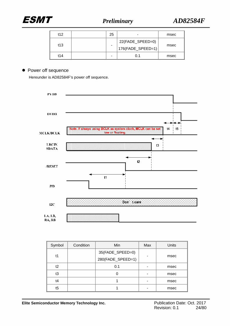
t12 25 - msec
t13
- 22(FADE_SPEED=0)
176(FADE_SPEED=1) msec
t14 - 0.1 msec
Power off sequence Hereunder is AD82584F’s power off sequence.
Symbol Condition Min Max Units
t1 35(FADE_SPEED=0)
280(FADE_SPEED=1) - msec
t2 0.1 - msec
t3 0 - msec
t4 1 - msec
t5 1 - msec
ESMT Preliminary AD82584F
Elite Semiconductor Memory Technology Inc. Publication Date: Oct. 2017 Revision: 0.1 25/80
I2C-Bus Transfer Protocol
Introduction AD82584F employs I2C-bus transfer protocol. Two wires, serial data and serial clock carry information
between the devices connected to the bus. Each device is recognized by a unique 7-bit address and can
operate as either a transmitter or a receiver. The master device initiates a data transfer and provides the
serial clock on the bus. AD82584F is always an I2C slave device.
Protocol
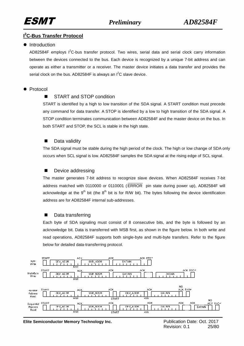
START and STOP condition START is identified by a high to low transition of the SDA signal. A START condition must precede
any command for data transfer. A STOP is identified by a low to high transition of the SDA signal. A
STOP condition terminates communication between AD82584F and the master device on the bus. In
both START and STOP, the SCL is stable in the high state.
Data validity The SDA signal must be stable during the high period of the clock. The high or low change of SDA only
occurs when SCL signal is low. AD82584F samples the SDA signal at the rising edge of SCL signal.
Device addressing The master generates 7-bit address to recognize slave devices. When AD82584F receives 7-bit
address matched with 0110000 or 0110001 ( ERROR pin state during power up), AD82584F will
acknowledge at the 9th bit (the 8th bit is for R/W bit). The bytes following the device identification
address are for AD82584F internal sub-addresses.
Data transferring Each byte of SDA signaling must consist of 8 consecutive bits, and the byte is followed by an
acknowledge bit. Data is transferred with MSB first, as shown in the figure below. In both write and
read operations, AD82584F supports both single-byte and multi-byte transfers. Refer to the figure
below for detailed data-transferring protocol.
ESMT Preliminary AD82584F
Elite Semiconductor Memory Technology Inc. Publication Date: Oct. 2017 Revision: 0.1 26/80
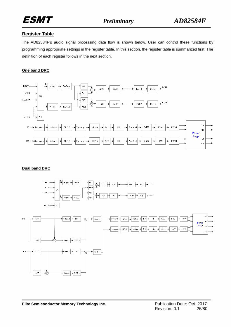
Register Table
The AD82584F’s audio signal processing data flow is shown below. User can control these functions by
programming appropriate settings in the register table. In this section, the register table is summarized first. The
definition of each register follows in the next section.
One band DRC
Dual band DRC
ESMT Preliminary AD82584F
Elite Semiconductor Memory Technology Inc. Publication Date: Oct. 2017 Revision: 0.1 27/80
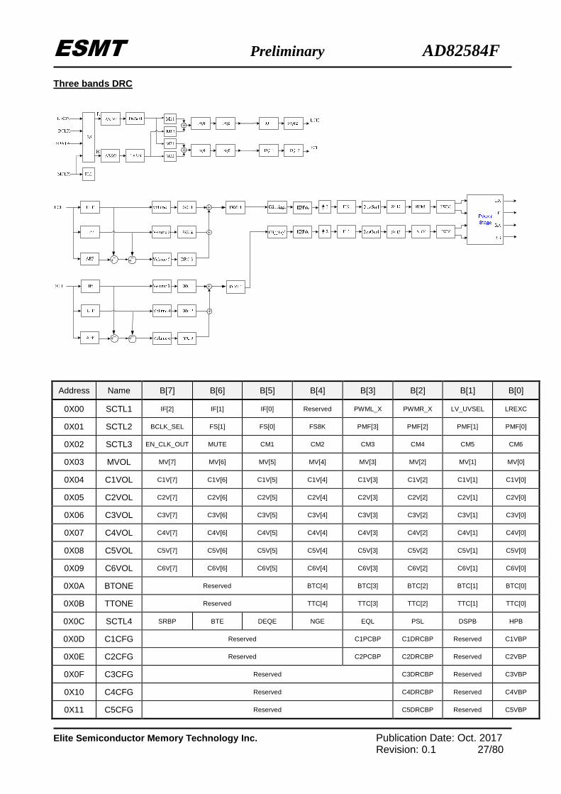
Three bands DRC
Address Name B[7] B[6] B[5] B[4] B[3] B[2] B[1] B[0]
0X00 SCTL1 IF[2] IF[1] IF[0] Reserved PWML_X PWMR_X LV_UVSEL LREXC
0X01 SCTL2 BCLK_SEL FS[1] FS[0] FS8K PMF[3] PMF[2] PMF[1] PMF[0]
0X02 SCTL3 EN_CLK_OUT MUTE CM1 CM2 CM3 CM4 CM5 CM6
0X03 MVOL MV[7] MV[6] MV[5] MV[4] MV[3] MV[2] MV[1] MV[0]
0X04 C1VOL C1V[7] C1V[6] C1V[5] C1V[4] C1V[3] C1V[2] C1V[1] C1V[0]
0X05 C2VOL C2V[7] C2V[6] C2V[5] C2V[4] C2V[3] C2V[2] C2V[1] C2V[0]
0X06 C3VOL C3V[7] C3V[6] C3V[5] C3V[4] C3V[3] C3V[2] C3V[1] C3V[0]
0X07 C4VOL C4V[7] C4V[6] C4V[5] C4V[4] C4V[3] C4V[2] C4V[1] C4V[0]
0X08 C5VOL C5V[7] C5V[6] C5V[5] C5V[4] C5V[3] C5V[2] C5V[1] C5V[0]
0X09 C6VOL C6V[7] C6V[6] C6V[5] C6V[4] C6V[3] C6V[2] C6V[1] C6V[0]
0X0A BTONE Reserved BTC[4] BTC[3] BTC[2] BTC[1] BTC[0]
0X0B TTONE Reserved TTC[4] TTC[3] TTC[2] TTC[1] TTC[0]
0X0C SCTL4 SRBP BTE DEQE NGE EQL PSL DSPB HPB
0X0D C1CFG Reserved C1PCBP C1DRCBP Reserved C1VBP
0X0E C2CFG Reserved C2PCBP C2DRCBP Reserved C2VBP
0X0F C3CFG Reserved C3DRCBP Reserved C3VBP
0X10 C4CFG Reserved C4DRCBP Reserved C4VBP
0X11 C5CFG Reserved C5DRCBP Reserved C5VBP
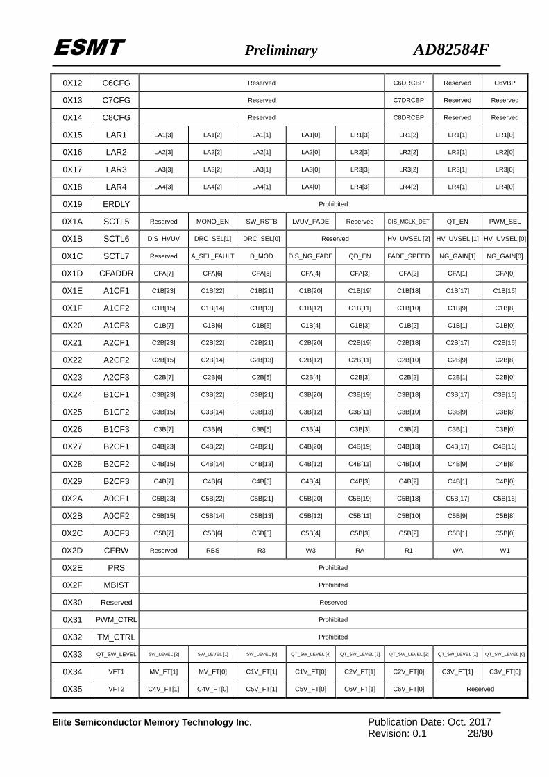
ESMT Preliminary AD82584F
Elite Semiconductor Memory Technology Inc. Publication Date: Oct. 2017 Revision: 0.1 28/80
0X12 C6CFG Reserved C6DRCBP Reserved C6VBP
0X13 C7CFG Reserved C7DRCBP Reserved Reserved
0X14 C8CFG Reserved C8DRCBP Reserved Reserved
0X15 LAR1 LA1[3] LA1[2] LA1[1] LA1[0] LR1[3] LR1[2] LR1[1] LR1[0]
0X16 LAR2 LA2[3] LA2[2] LA2[1] LA2[0] LR2[3] LR2[2] LR2[1] LR2[0]
0X17 LAR3 LA3[3] LA3[2] LA3[1] LA3[0] LR3[3] LR3[2] LR3[1] LR3[0]
0X18 LAR4 LA4[3] LA4[2] LA4[1] LA4[0] LR4[3] LR4[2] LR4[1] LR4[0]
0X19 ERDLY Prohibited
0X1A SCTL5 Reserved MONO_EN SW_RSTB LVUV_FADE Reserved DIS_MCLK_DET QT_EN PWM_SEL
0X1B SCTL6 DIS_HVUV DRC_SEL[1] DRC_SEL[0] Reserved HV_UVSEL [2] HV_UVSEL [1] HV_UVSEL [0]
0X1C SCTL7 Reserved A_SEL_FAULT D_MOD DIS_NG_FADE QD_EN FADE_SPEED NG_GAIN[1] NG_GAIN[0]
0X1D CFADDR CFA[7] CFA[6] CFA[5] CFA[4] CFA[3] CFA[2] CFA[1] CFA[0]
0X1E A1CF1 C1B[23] C1B[22] C1B[21] C1B[20] C1B[19] C1B[18] C1B[17] C1B[16]
0X1F A1CF2 C1B[15] C1B[14] C1B[13] C1B[12] C1B[11] C1B[10] C1B[9] C1B[8]
0X20 A1CF3 C1B[7] C1B[6] C1B[5] C1B[4] C1B[3] C1B[2] C1B[1] C1B[0]
0X21 A2CF1 C2B[23] C2B[22] C2B[21] C2B[20] C2B[19] C2B[18] C2B[17] C2B[16]
0X22 A2CF2 C2B[15] C2B[14] C2B[13] C2B[12] C2B[11] C2B[10] C2B[9] C2B[8]
0X23 A2CF3 C2B[7] C2B[6] C2B[5] C2B[4] C2B[3] C2B[2] C2B[1] C2B[0]
0X24 B1CF1 C3B[23] C3B[22] C3B[21] C3B[20] C3B[19] C3B[18] C3B[17] C3B[16]
0X25 B1CF2 C3B[15] C3B[14] C3B[13] C3B[12] C3B[11] C3B[10] C3B[9] C3B[8]
0X26 B1CF3 C3B[7] C3B[6] C3B[5] C3B[4] C3B[3] C3B[2] C3B[1] C3B[0]
0X27 B2CF1 C4B[23] C4B[22] C4B[21] C4B[20] C4B[19] C4B[18] C4B[17] C4B[16]
0X28 B2CF2 C4B[15] C4B[14] C4B[13] C4B[12] C4B[11] C4B[10] C4B[9] C4B[8]
0X29 B2CF3 C4B[7] C4B[6] C4B[5] C4B[4] C4B[3] C4B[2] C4B[1] C4B[0]
0X2A A0CF1 C5B[23] C5B[22] C5B[21] C5B[20] C5B[19] C5B[18] C5B[17] C5B[16]
0X2B A0CF2 C5B[15] C5B[14] C5B[13] C5B[12] C5B[11] C5B[10] C5B[9] C5B[8]
0X2C A0CF3 C5B[7] C5B[6] C5B[5] C5B[4] C5B[3] C5B[2] C5B[1] C5B[0]
0X2D CFRW Reserved RBS R3 W3 RA R1 WA W1
0X2E PRS Prohibited
0X2F MBIST Prohibited
0X30 Reserved Reserved
0X31 PWM_CTRL Prohibited
0X32 TM_CTRL Prohibited
0X33 QT_SW_LEVEL SW_LEVEL [2] SW_LEVEL [1] SW_LEVEL [0] QT_SW_LEVEL [4] QT_SW_LEVEL [3] QT_SW_LEVEL [2] QT_SW_LEVEL [1] QT_SW_LEVEL [0]
0X34 VFT1 MV_FT[1] MV_FT[0] C1V_FT[1] C1V_FT[0] C2V_FT[1] C2V_FT[0] C3V_FT[1] C3V_FT[0]
0X35 VFT2 C4V_FT[1] C4V_FT[0] C5V_FT[1] C5V_FT[0] C6V_FT[1] C6V_FT[0] Reserved
ESMT Preliminary AD82584F
Elite Semiconductor Memory Technology Inc. Publication Date: Oct. 2017 Revision: 0.1 29/80
0X36 OCB_GVDDS Prohibited
0X37 ID DN[3] DN[2] DN[1] DN[0] VN[3] VN[2] VN[1] VN[0]
0X38 R1ADDR Prohibited
0X39 R1D1 Prohibited
0X3A R1D2 Prohibited
0X3B R1D3 Prohibited
0X3C R1RW Prohibited
0X3D R2ADDR Prohibited
0X3E R2D1 Prohibited
0X3F R2D2 Prohibited
0X40 R2D3 Prohibited
0X41 R2RW Prohibited
0X42 LMC C1_CLR C2_CLR C3_CLR C4_CLR C5_CLR C6_CLR C7_CLR C8_CLR
0X43 PMC C1_CLR_RMS C2_CLR_RMS C3_CLR_RMS C4_CLR_RMS C5_CLR_RMS C6_CLR_RMS C7_CLR_RMS C8_CLR_RMS
0X44 TC1LM C1_LEVEL[23] C1_LEVEL[22] C1_LEVEL[21] C1_LEVEL[20] C1_LEVEL[19] C1_LEVEL[18] C1_LEVEL[17] C1_LEVEL[16]
0X45 MC1LM C1_LEVEL[15] C1_LEVEL[14] C1_LEVEL[13] C1_LEVEL[12] C1_LEVEL[11] C1_LEVEL[10] C1_LEVEL[9] C1_LEVEL[8]
0X46 BC1LM C1_LEVEL[7] C1_LEVEL[6] C1_LEVEL[5] C1_LEVEL[4] C1_LEVEL[3] C1_LEVEL[2] C1_LEVEL[1] C1_LEVEL[0]
0X47 TC2LM C2_LEVEL[23] C2_LEVEL[22] C2_LEVEL[21] C2_LEVEL[20] C2_LEVEL[19] C2_LEVEL[18] C2_LEVEL[17] C2_LEVEL[16]
0X48 MC2LM C2_LEVEL[15] C2_LEVEL[14] C2_LEVEL[13] C2_LEVEL[12] C2_LEVEL[11] C2_LEVEL[10] C2_LEVEL[9] C2_LEVEL[8]
0X49 BC2LM C2_LEVEL[7] C2_LEVEL[6] C2_LEVEL[5] C2_LEVEL[4] C2_LEVEL[3] C2_LEVEL[2] C2_LEVEL[1] C2_LEVEL[0]
0X4A TC3LM C3_LEVEL[23] C3_LEVEL[22] C3_LEVEL[21] C3_LEVEL[20] C3_LEVEL[19] C3_LEVEL[18] C3_LEVEL[17] C3_LEVEL[16]
0X4B MC3LM C3_LEVEL[15] C3_LEVEL[14] C3_LEVEL[13] C3_LEVEL[12] C3_LEVEL[11] C3_LEVEL[10] C3_LEVEL[9] C3_LEVEL[8]
0X4C BC3LM C3_LEVEL[7] C3_LEVEL[6] C3_LEVEL[5] C3_LEVEL[4] C3_LEVEL[3] C3_LEVEL[2] C3_LEVEL[1] C3_LEVEL[0]
0X4D TC4LM C4_LEVEL[23] C4_LEVEL[22] C4_LEVEL[21] C4_LEVEL[20] C4_LEVEL[19] C4_LEVEL[18] C4_LEVEL[17] C4_LEVEL[16]
0X4E MC4LM C4_LEVEL[15] C4_LEVEL[14] C4_LEVEL[13] C4_LEVEL[12] C4_LEVEL[11] C4_LEVEL[10] C4_LEVEL[9] C4_LEVEL[8]
0X4F BC4LM C4_LEVEL[7] C4_LEVEL[6] C4_LEVEL[5] C4_LEVEL[4] C4_LEVEL[3] C4_LEVEL[2] C4_LEVEL[1] C4_LEVEL[0]
0X50 TC5LM C5_LEVEL[23] C5_LEVEL[22] C5_LEVEL[21] C5_LEVEL[20] C5_LEVEL[19] C5_LEVEL[18] C5_LEVEL[17] C5_LEVEL[16]
0X51 MC5LM C5_LEVEL[15] C5_LEVEL[14] C5_LEVEL[13] C5_LEVEL[12] C5_LEVEL[11] C5_LEVEL[10] C5_LEVEL[9] C5_LEVEL[8]
0X52 BC5LM C5_LEVEL[7] C5_LEVEL[6] C5_LEVEL[5] C5_LEVEL[4] C5_LEVEL[3] C5_LEVEL[2] C5_LEVEL[1] C5_LEVEL[0]
0X53 TC6LM C6_LEVEL[23] C6_LEVEL[22] C6_LEVEL[21] C6_LEVEL[20] C6_LEVEL[19] C6_LEVEL[18] C6_LEVEL[17] C6_LEVEL[16]
0X54 MC6LM C6_LEVEL[15] C6_LEVEL[14] C6_LEVEL[13] C6_LEVEL[12] C6_LEVEL[11] C6_LEVEL[10] C6_LEVEL[9] C6_LEVEL[8]
0X55 BC6LM C6_LEVEL[7] C6_LEVEL[6] C6_LEVEL[5] C6_LEVEL[4] C6_LEVEL[3] C6_LEVEL[2] C6_LEVEL[1] C6_LEVEL[0]
0X56 TC7LM C7_LEVEL[23] C7_LEVEL[22] C7_LEVEL[21] C7_LEVEL[20] C7_LEVEL[19] C7_LEVEL[18] C7_LEVEL[17] C7_LEVEL[16]
0X57 MC7LM C7_LEVEL[15] C7_LEVEL[14] C7_LEVEL[13] C7_LEVEL[12] C7_LEVEL[11] C7_LEVEL[10] C7_LEVEL[9] C7_LEVEL[8]
0X58 BC7LM C7_LEVEL[7] C7_LEVEL[6] C7_LEVEL[5] C7_LEVEL[4] C7_LEVEL[3] C7_LEVEL[2] C7_LEVEL[1] C7_LEVEL[0]
0X59 TC8LM C8_LEVEL[23] C8_LEVEL[22] C8_LEVEL[21] C8_LEVEL[20] C8_LEVEL[19] C8_LEVEL[18] C8_LEVEL[17] C8_LEVEL[16]
ESMT Preliminary AD82584F
Elite Semiconductor Memory Technology Inc. Publication Date: Oct. 2017 Revision: 0.1 30/80
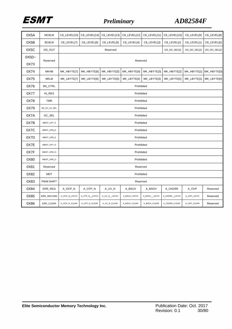
0X5A MC8LM C8_LEVEL[15] C8_LEVEL[14] C8_LEVEL[13] C8_LEVEL[12] C8_LEVEL[11] C8_LEVEL[10] C8_LEVEL[9] C8_LEVEL[8]
0X5B BC8LM C8_LEVEL[7] C8_LEVEL[6] C8_LEVEL[5] C8_LEVEL[4] C8_LEVEL[3] C8_LEVEL[2] C8_LEVEL[1] C8_LEVEL[0]
0X5C I2S_OUT Reserved I2S_DO_SEL[2] I2S_DO_SEL[2] I2S_DO_SEL[2]
0X5D~
0X73 Reserved Reserved
0X74 MKHB MK_HBYTE[7] MK_HBYTE[6] MK_HBYTE[5] MK_HBYTE[4] MK_HBYTE[3] MK_HBYTE[2] MK_HBYTE[1] MK_HBYTE[0]
0X75 MKLB MK_LBYTE[7] MK_LBYTE[6] MK_LBYTE[5] MK_LBYTE[4] MK_LBYTE[3] MK_LBYTE[2] MK_LBYTE[1] MK_LBYTE[0]
0X76 BS_CTRL Prohibited
0X77 HI_RES Prohibited
0X78 TMR Prohibited
0X79 BS_OV_UV_SEL Prohibited
0X7A OC_SEL Prohibited
0X7B MBIST_UPT_E Prohibited
0X7C MBIST_UPM_E Prohibited
0X7D MBIST_UPB_E Prohibited
0X7E MBIST_UPT_O Prohibited
0X7F MBIST_UPM_O Prohibited
0X80 MBIST_UPB_O Prohibited
0X81 Reserved Reserved
0X82 MDT Prohibited
0X83 PWM SHIFT Reserved
0X84 ERR_REG A_OCP_N A_OTP_N A_UV_N A_BSUV A_BSOV A_CKERR A_OVP Reserved
0X85 ERR_RECORD A_OCP_N_LATCH A_OTP_N__LATCH A_UV_N__LATCH A_BSUV_LATCH A_BSOV__LATCH A_CKERR__LATCH A_OVP_LATCH Reserved
0X86 ERR_CLEAR A_OCP_N_CLEAR A_OTP_N_CLEAR A_UV_N_CLEAR A_BSUV_CLEAR A_BSOV_CLEAR A_CKERR_CLEAR A_OVP_CLEAR Reserved
ESMT Preliminary AD82584F
Elite Semiconductor Memory Technology Inc. Publication Date: Oct. 2017 Revision: 0.1 31/80
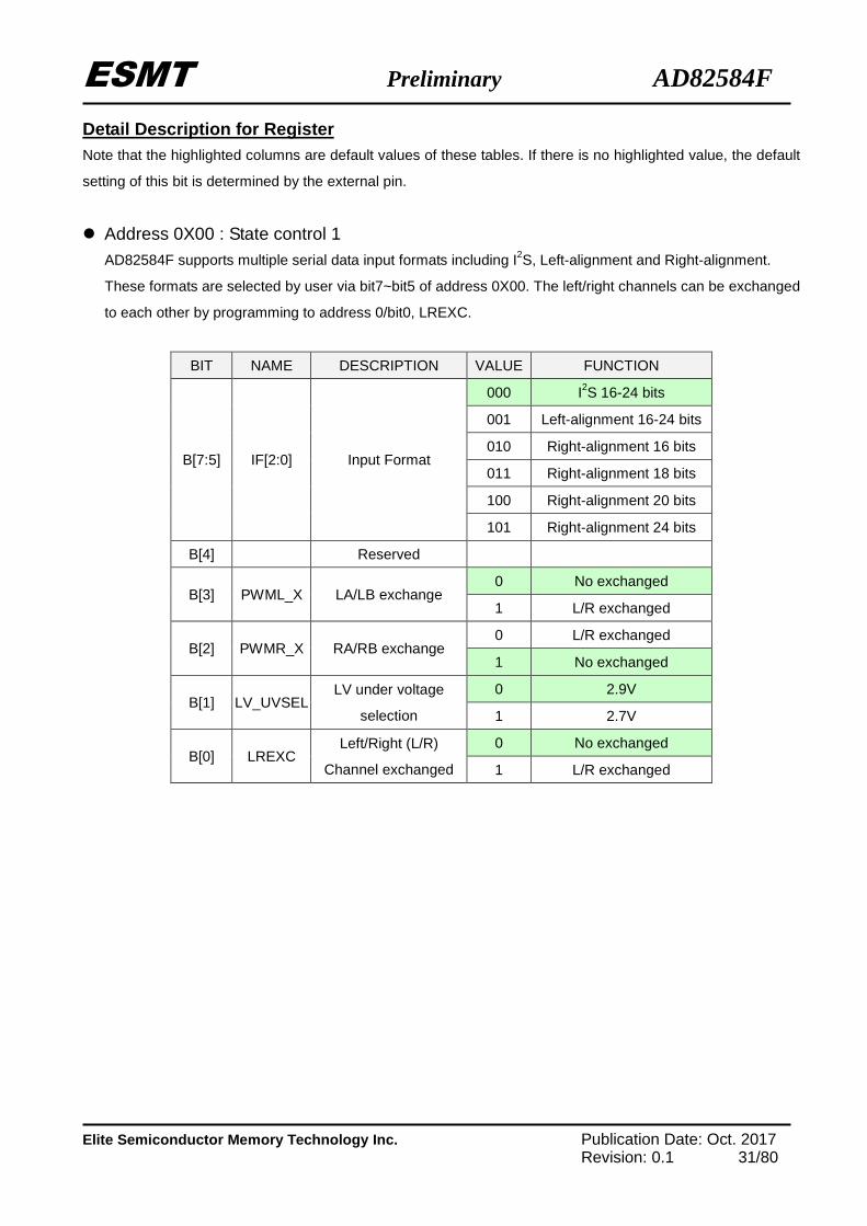
Detail Description for Register Note that the highlighted columns are default values of these tables. If there is no highlighted value, the default
setting of this bit is determined by the external pin.
Address 0X00 : State control 1 AD82584F supports multiple serial data input formats including I2S, Left-alignment and Right-alignment.
These formats are selected by user via bit7~bit5 of address 0X00. The left/right channels can be exchanged
to each other by programming to address 0/bit0, LREXC.
BIT NAME DESCRIPTION VALUE FUNCTION
B[7:5] IF[2:0] Input Format
000 I2S 16-24 bits
001 Left-alignment 16-24 bits
010 Right-alignment 16 bits
011 Right-alignment 18 bits
100 Right-alignment 20 bits
101 Right-alignment 24 bits
B[4] Reserved
B[3] PWML_X LA/LB exchange 0 No exchanged
1 L/R exchanged
B[2] PWMR_X RA/RB exchange 0 L/R exchanged
1 No exchanged
B[1] LV_UVSEL LV under voltage
selection
0 2.9V
1 2.7V
B[0] LREXC Left/Right (L/R)
Channel exchanged
0 No exchanged
1 L/R exchanged
ESMT Preliminary AD82584F
Elite Semiconductor Memory Technology Inc. Publication Date: Oct. 2017 Revision: 0.1 32/80
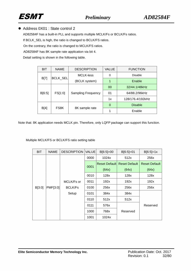
Address 0X01 : State control 2 AD82584F has a built-in PLL and supports multiple MCLK/Fs or BCLK/Fs ratios.
If BCLK_SEL is high, the ratio is changed to BCLK/FS ratios.
On the contrary, the ratio is changed to MCLK/FS ratios.
AD82584F has 8K sample rate application via bit 4.
Detail setting is shown in the following table.
BIT NAME DESCRIPTION VALUE FUNCTION
B[7] BCLK_SEL MCLK-less
(BCLK system)
0 Disable
1 Enable
B[6:5] FS[1:0] Sampling Frequency
00 32/44.1/48kHz
01 64/88.2/96kHz
1x 128/176.4/192kHz
B[4] FS8K 8K sample rate 0 Disable
1 Enable
Note that: 8K application needs MCLK pin. Therefore, only LQFP package can support this function.
Multiple MCLK/FS or BCLK/FS ratio setting table
BIT NAME DESCRIPTION VALUE B[6:5]=00 B[6:5]=01 B[6:5]=1x
B[3:0] PMF[3:0]
MCLK/Fs or
BCLK/Fs
Setup
0000 1024x 512x 256x
0001 Reset Default
(64x)
Reset Default
(64x)
Reset Default
(64x)
0010 128x 128x 128x
0011 192x 192x 192x
0100 256x 256x 256x
0101 384x 384x
Reserved
0110 512x 512x
0111 576x
Reserved 1000 768x
1001 1024x
ESMT Preliminary AD82584F
Elite Semiconductor Memory Technology Inc. Publication Date: Oct. 2017 Revision: 0.1 33/80
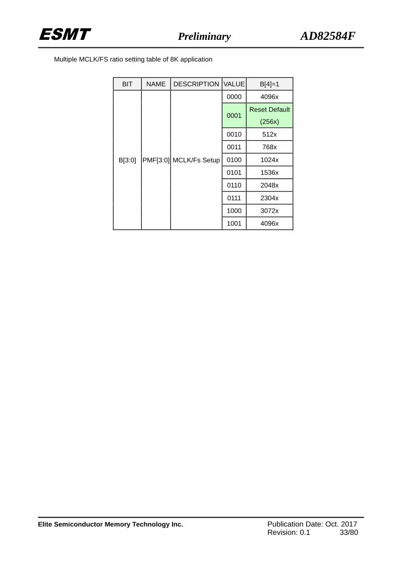
Multiple MCLK/FS ratio setting table of 8K application
BIT NAME DESCRIPTION VALUE B[4]=1
B[3:0] PMF[3:0] MCLK/Fs Setup
0000 4096x
0001 Reset Default
(256x)
0010 512x
0011 768x
0100 1024x
0101 1536x
0110 2048x
0111 2304x
1000 3072x
1001 4096x
ESMT Preliminary AD82584F
Elite Semiconductor Memory Technology Inc. Publication Date: Oct. 2017 Revision: 0.1 34/80
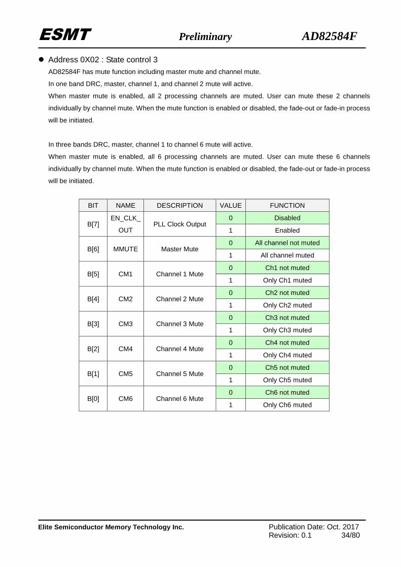
Address 0X02 : State control 3 AD82584F has mute function including master mute and channel mute.
In one band DRC, master, channel 1, and channel 2 mute will active.
When master mute is enabled, all 2 processing channels are muted. User can mute these 2 channels
individually by channel mute. When the mute function is enabled or disabled, the fade-out or fade-in process
will be initiated.
In three bands DRC, master, channel 1 to channel 6 mute will active.
When master mute is enabled, all 6 processing channels are muted. User can mute these 6 channels
individually by channel mute. When the mute function is enabled or disabled, the fade-out or fade-in process
will be initiated.
BIT NAME DESCRIPTION VALUE FUNCTION
B[7] EN_CLK_
OUT PLL Clock Output
0 Disabled
1 Enabled
B[6] MMUTE Master Mute 0 All channel not muted
1 All channel muted
B[5] CM1 Channel 1 Mute 0 Ch1 not muted
1 Only Ch1 muted
B[4] CM2 Channel 2 Mute 0 Ch2 not muted
1 Only Ch2 muted
B[3] CM3 Channel 3 Mute 0 Ch3 not muted
1 Only Ch3 muted
B[2] CM4 Channel 4 Mute 0 Ch4 not muted
1 Only Ch4 muted
B[1] CM5 Channel 5 Mute 0 Ch5 not muted
1 Only Ch5 muted
B[0] CM6 Channel 6 Mute 0 Ch6 not muted
1 Only Ch6 muted
ESMT Preliminary AD82584F
Elite Semiconductor Memory Technology Inc. Publication Date: Oct. 2017 Revision: 0.1 35/80
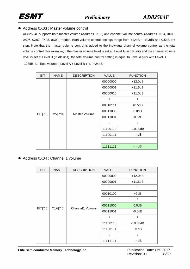
Address 0X03 : Master volume control AD82584F supports both master-volume (Address 0X03) and channel-volume control (Address 0X04, 0X05,
0X06, 0X07, 0X08, 0X09) modes. Both volume control settings range from +12dB ~ -103dB and 0.5dB per
step. Note that the master volume control is added to the individual channel volume control as the total
volume control. For example, if the master volume level is set at, Level A (in dB unit) and the channel volume
level is set at Level B (in dB unit), the total volume control setting is equal to Level A plus with Level B.
-103dB ≦ Total volume ( Level A + Level B ) ≦ +24dB.
BIT NAME DESCRIPTION VALUE FUNCTION
BIT[7:0] MV[7:0] Master Volume
00000000 +12.0dB
00000001 +11.5dB
00000010 +11.0dB
︰ ︰
00010111 +0.5dB
00011000 0.0dB
00011001 -0.5dB
︰ ︰
11100110 -103.0dB
11100111 -∞dB
︰ ︰
11111111 -∞dB
Address 0X04 : Channel 1 volume
BIT NAME DESCRIPTION VALUE FUNCTION
BIT[7:0] C1V[7:0] Channel1 Volume
00000000 +12.0dB
00000001 +11.5dB
︰ ︰
00010100 +2dB
︰ ︰
00011000 0.0dB
00011001 -0.5dB
︰ ︰
11100110 -103.0dB
11100111 -∞dB
︰ ︰
11111111 -∞dB
ESMT Preliminary AD82584F
Elite Semiconductor Memory Technology Inc. Publication Date: Oct. 2017 Revision: 0.1 36/80
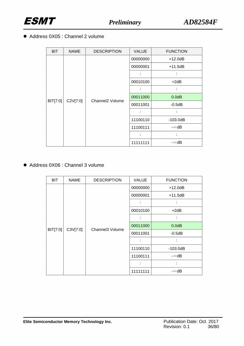
Address 0X05 : Channel 2 volume
BIT NAME DESCRIPTION VALUE FUNCTION
BIT[7:0] C2V[7:0] Channel2 Volume
00000000 +12.0dB
00000001 +11.5dB
︰ ︰
00010100 +2dB
︰ ︰
00011000 0.0dB
00011001 -0.5dB
︰ ︰
11100110 -103.0dB
11100111 -∞dB
︰ ︰
11111111 -∞dB
Address 0X06 : Channel 3 volume
BIT NAME DESCRIPTION VALUE FUNCTION
BIT[7:0] C3V[7:0] Channel3 Volume
00000000 +12.0dB
00000001 +11.5dB
︰ ︰
00010100 +2dB
︰ ︰
00011000 0.0dB
00011001 -0.5dB
︰ ︰
11100110 -103.0dB
11100111 -∞dB
︰ ︰
11111111 -∞dB
ESMT Preliminary AD82584F
Elite Semiconductor Memory Technology Inc. Publication Date: Oct. 2017 Revision: 0.1 37/80
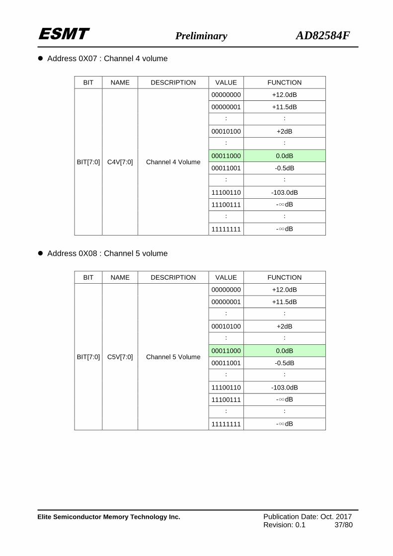
Address 0X07 : Channel 4 volume
BIT NAME DESCRIPTION VALUE FUNCTION
BIT[7:0] C4V[7:0] Channel 4 Volume
00000000 +12.0dB
00000001 +11.5dB
︰ ︰
00010100 +2dB
︰ ︰
00011000 0.0dB
00011001 -0.5dB
︰ ︰
11100110 -103.0dB
11100111 -∞dB
︰ ︰
11111111 -∞dB
Address 0X08 : Channel 5 volume
BIT NAME DESCRIPTION VALUE FUNCTION
BIT[7:0] C5V[7:0] Channel 5 Volume
00000000 +12.0dB
00000001 +11.5dB
︰ ︰
00010100 +2dB
︰ ︰
00011000 0.0dB
00011001 -0.5dB
︰ ︰
11100110 -103.0dB
11100111 -∞dB
︰ ︰
11111111 -∞dB
ESMT Preliminary AD82584F
Elite Semiconductor Memory Technology Inc. Publication Date: Oct. 2017 Revision: 0.1 38/80
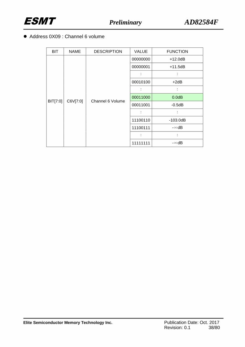
Address 0X09 : Channel 6 volume
BIT NAME DESCRIPTION VALUE FUNCTION
BIT[7:0] C6V[7:0] Channel 6 Volume
00000000 +12.0dB
00000001 +11.5dB
︰ ︰
00010100 +2dB
︰ ︰
00011000 0.0dB
00011001 -0.5dB
︰ ︰
11100110 -103.0dB
11100111 -∞dB
︰ ︰
11111111 -∞dB
ESMT Preliminary AD82584F
Elite Semiconductor Memory Technology Inc. Publication Date: Oct. 2017 Revision: 0.1 39/80
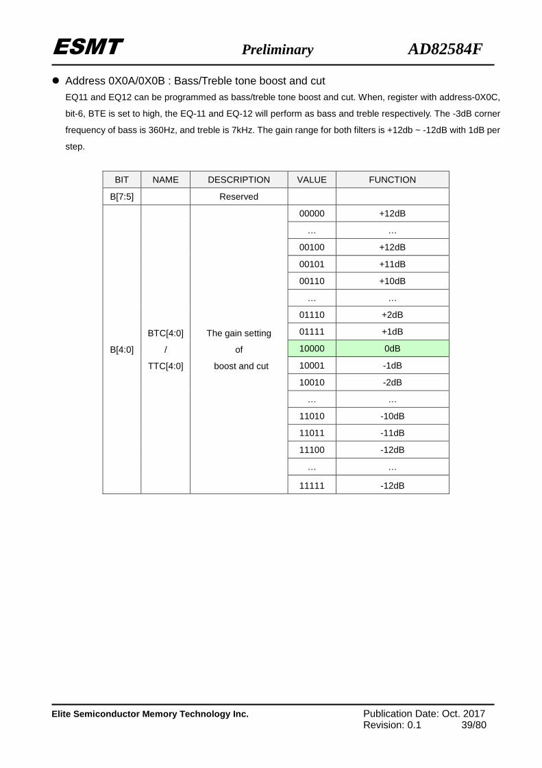
Address 0X0A/0X0B : Bass/Treble tone boost and cut EQ11 and EQ12 can be programmed as bass/treble tone boost and cut. When, register with address-0X0C,
bit-6, BTE is set to high, the EQ-11 and EQ-12 will perform as bass and treble respectively. The -3dB corner
frequency of bass is 360Hz, and treble is 7kHz. The gain range for both filters is +12db ~ -12dB with 1dB per
step.
BIT NAME DESCRIPTION VALUE FUNCTION
B[7:5] Reserved
B[4:0]
BTC[4:0]
/
TTC[4:0]
The gain setting
of
boost and cut
00000 +12dB
… …
00100 +12dB
00101 +11dB
00110 +10dB
… …
01110 +2dB
01111 +1dB
10000 0dB
10001 -1dB
10010 -2dB
… …
11010 -10dB
11011 -11dB
11100 -12dB
… …
11111 -12dB
ESMT Preliminary AD82584F
Elite Semiconductor Memory Technology Inc. Publication Date: Oct. 2017 Revision: 0.1 40/80
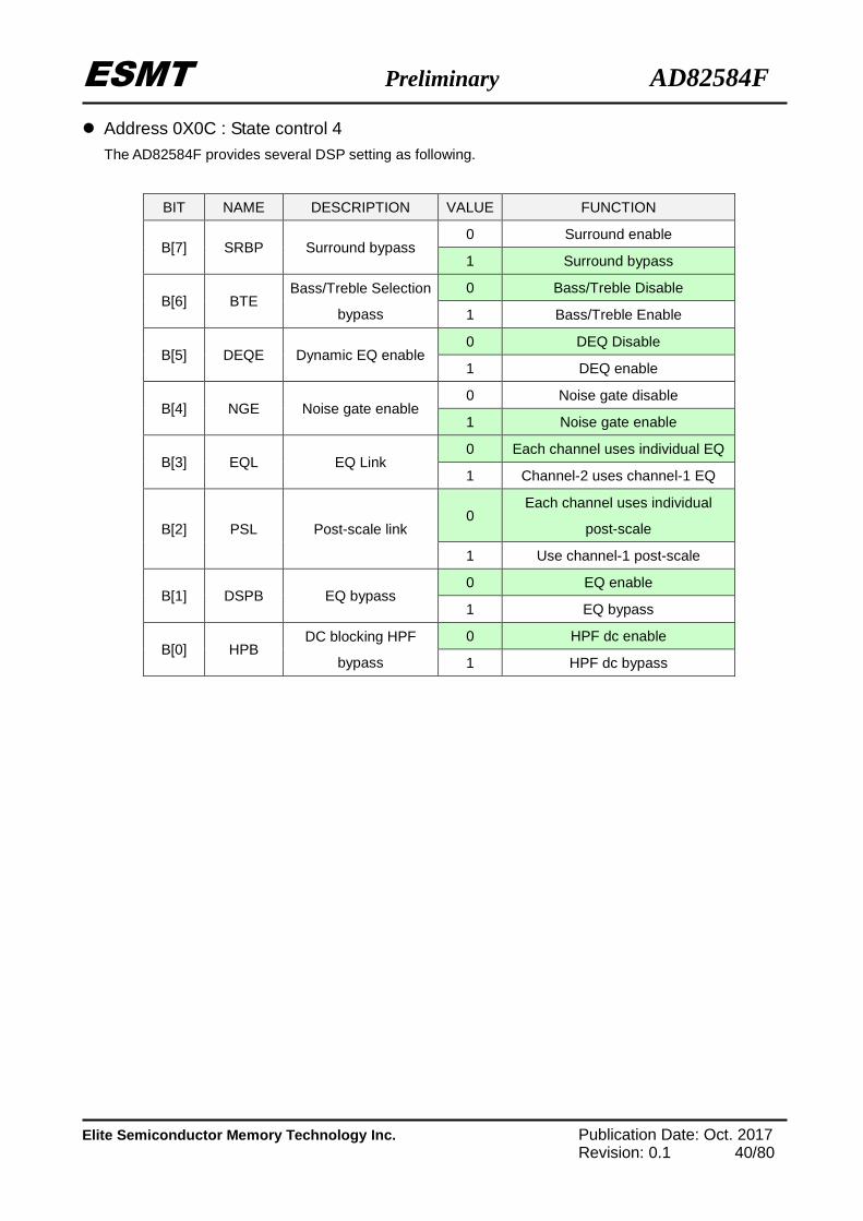
Address 0X0C : State control 4 The AD82584F provides several DSP setting as following.
BIT NAME DESCRIPTION VALUE FUNCTION
B[7] SRBP Surround bypass 0 Surround enable
1 Surround bypass
B[6] BTE Bass/Treble Selection
bypass
0 Bass/Treble Disable
1 Bass/Treble Enable
B[5] DEQE Dynamic EQ enable 0 DEQ Disable
1 DEQ enable
B[4] NGE Noise gate enable 0 Noise gate disable
1 Noise gate enable
B[3] EQL EQ Link 0 Each channel uses individual EQ
1 Channel-2 uses channel-1 EQ
B[2] PSL Post-scale link 0
Each channel uses individual
post-scale
1 Use channel-1 post-scale
B[1] DSPB EQ bypass 0 EQ enable
1 EQ bypass
B[0] HPB DC blocking HPF
bypass
0 HPF dc enable
1 HPF dc bypass
ESMT Preliminary AD82584F
Elite Semiconductor Memory Technology Inc. Publication Date: Oct. 2017 Revision: 0.1 41/80
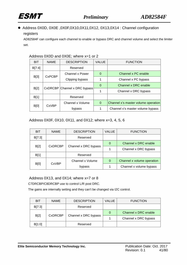
Address 0X0D, 0X0E ,0X0F,0X10,0X11,0X12, 0X13,0X14 : Channel configuration
registers AD82584F can configure each channel to enable or bypass DRC and channel volume and select the limiter
set.
Address 0X0D and 0X0E; where x=1 or 2
BIT NAME DESCRIPTION VALUE FUNCTION
B[7:4] Reserved
B[3] CxPCBP Channel x Power
Clipping bypass
0 Channel x PC enable
1 Channel x PC bypass
B[2] CxDRCBP Channel x DRC bypass 0 Channel x DRC enable
1 Channel x DRC bypass
B[1] Reserved
B[0] CxVBP Channel x Volume
bypass
0 Channel x’s master volume operation
1 Channel x’s master volume bypass
Address 0X0F, 0X10, 0X11, and 0X12; where x=3, 4, 5, 6
BIT NAME DESCRIPTION VALUE FUNCTION
B[7:3] Reserved
B[2] CxDRCBP Channel x DRC bypass 0 Channel x DRC enable
1 Channel x DRC bypass
B[1] Reserved
B[0] CxVBP Channel x Volume
bypass
0 Channel x volume operation
1 Channel x volume bypass
Address 0X13, and 0X14; where x=7 or 8 C7DRCBP/C8DRCBP use to control L/R post DRC.
The gains are internally setting and they can’t be changed via I2C control.
BIT NAME DESCRIPTION VALUE FUNCTION
B[7:3] Reserved
B[2] CxDRCBP Channel x DRC bypass 0 Channel x DRC enable
1 Channel x DRC bypass
B[1:0] Reserved
ESMT Preliminary AD82584F
Elite Semiconductor Memory Technology Inc. Publication Date: Oct. 2017 Revision: 0.1 42/80
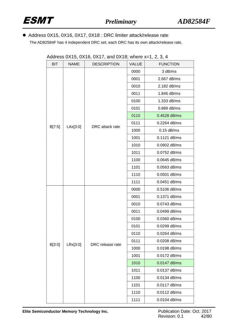
Address 0X15, 0X16, 0X17, 0X18 : DRC limiter attack/release rate The AD82584F has 4 independent DRC set, each DRC has its own attack/release rate.
Address 0X15, 0X16, 0X17, and 0X18; where x=1, 2, 3, 4
BIT NAME DESCRIPTION VALUE FUNCTION
B[7:5] LAx[3:0] DRC attack rate
0000 3 dB/ms
0001 2.667 dB/ms
0010 2.182 dB/ms
0011 1.846 dB/ms
0100 1.333 dB/ms
0101 0.889 dB/ms
0110 0.4528 dB/ms
0111 0.2264 dB/ms
1000 0.15 dB/ms
1001 0.1121 dB/ms
1010 0.0902 dB/ms
1011 0.0752 dB/ms
1100 0.0645 dB/ms
1101 0.0563 dB/ms
1110 0.0501 dB/ms
1111 0.0451 dB/ms
B[3:0] LRx[3:0] DRC release rate
0000 0.5106 dB/ms
0001 0.1371 dB/ms
0010 0.0743 dB/ms
0011 0.0499 dB/ms
0100 0.0360 dB/ms
0101 0.0299 dB/ms
0110 0.0264 dB/ms
0111 0.0208 dB/ms
1000 0.0198 dB/ms
1001 0.0172 dB/ms
1010 0.0147 dB/ms
1011 0.0137 dB/ms
1100 0.0134 dB/ms
1101 0.0117 dB/ms
1110 0.0112 dB/ms
1111 0.0104 dB/ms
ESMT Preliminary AD82584F
Elite Semiconductor Memory Technology Inc. Publication Date: Oct. 2017 Revision: 0.1 43/80
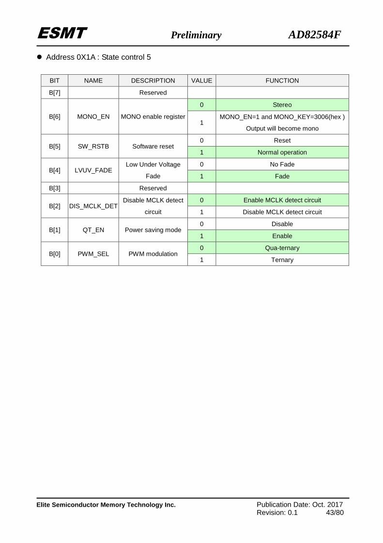
Address 0X1A : State control 5
BIT NAME DESCRIPTION VALUE FUNCTION
B[7] Reserved
B[6] MONO_EN MONO enable register
0 Stereo
1 MONO_EN=1 and MONO_KEY=3006(hex )
Output will become mono
B[5] SW_RSTB Software reset 0 Reset
1 Normal operation
B[4] LVUV_FADE Low Under Voltage
Fade
0 No Fade
1 Fade
B[3] Reserved
B[2] DIS_MCLK_DET Disable MCLK detect
circuit
0 Enable MCLK detect circuit
1 Disable MCLK detect circuit
B[1] QT_EN Power saving mode 0 Disable
1 Enable
B[0] PWM_SEL PWM modulation 0 Qua-ternary
1 Ternary
ESMT Preliminary AD82584F
Elite Semiconductor Memory Technology Inc. Publication Date: Oct. 2017 Revision: 0.1 44/80
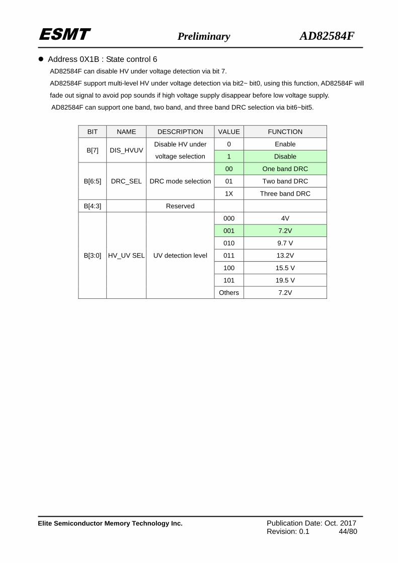
Address 0X1B : State control 6 AD82584F can disable HV under voltage detection via bit 7.
AD82584F support multi-level HV under voltage detection via bit2~ bit0, using this function, AD82584F will
fade out signal to avoid pop sounds if high voltage supply disappear before low voltage supply.
AD82584F can support one band, two band, and three band DRC selection via bit6~bit5.
BIT NAME DESCRIPTION VALUE FUNCTION
B[7] DIS_HVUV Disable HV under
voltage selection
0 Enable
1 Disable
B[6:5] DRC_SEL DRC mode selection
00 One band DRC
01 Two band DRC
1X Three band DRC
B[4:3] Reserved
B[3:0] HV_UV SEL UV detection level
000 4V
001 7.2V
010 9.7 V
011 13.2V
100 15.5 V
101 19.5 V
Others 7.2V
ESMT Preliminary AD82584F
Elite Semiconductor Memory Technology Inc. Publication Date: Oct. 2017 Revision: 0.1 45/80
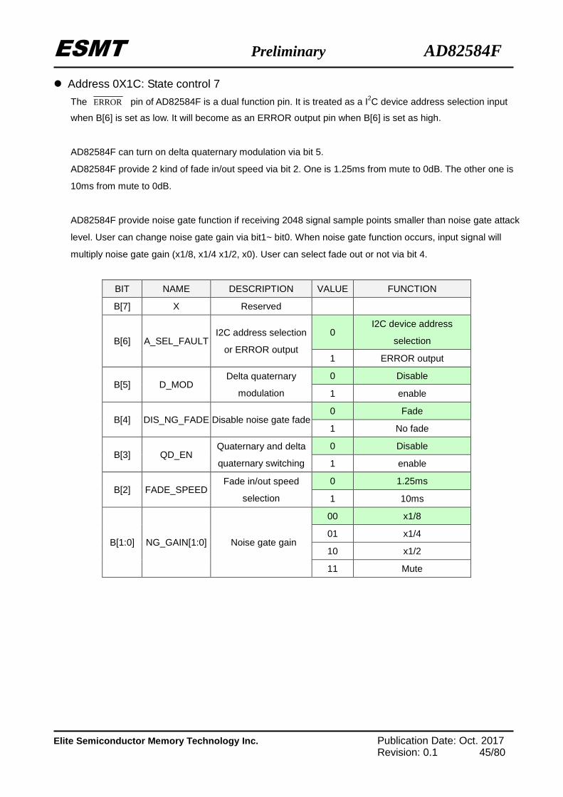
Address 0X1C: State control 7
The ERROR pin of AD82584F is a dual function pin. It is treated as a I2C device address selection input
when B[6] is set as low. It will become as an ERROR output pin when B[6] is set as high.
AD82584F can turn on delta quaternary modulation via bit 5.
AD82584F provide 2 kind of fade in/out speed via bit 2. One is 1.25ms from mute to 0dB. The other one is
10ms from mute to 0dB.
AD82584F provide noise gate function if receiving 2048 signal sample points smaller than noise gate attack
level. User can change noise gate gain via bit1~ bit0. When noise gate function occurs, input signal will
multiply noise gate gain (x1/8, x1/4 x1/2, x0). User can select fade out or not via bit 4.
BIT NAME DESCRIPTION VALUE FUNCTION
B[7] X Reserved
B[6] A_SEL_FAULT I2C address selection
or ERROR output
0 I2C device address
selection
1 ERROR output
B[5] D_MOD Delta quaternary
modulation
0 Disable
1 enable
B[4] DIS_NG_FADE Disable noise gate fade 0 Fade
1 No fade
B[3] QD_EN Quaternary and delta
quaternary switching
0 Disable
1 enable
B[2] FADE_SPEED Fade in/out speed
selection
0 1.25ms
1 10ms
B[1:0] NG_GAIN[1:0] Noise gate gain
00 x1/8
01 x1/4
10 x1/2
11 Mute
ESMT Preliminary AD82584F
Elite Semiconductor Memory Technology Inc. Publication Date: Oct. 2017 Revision: 0.1 46/80
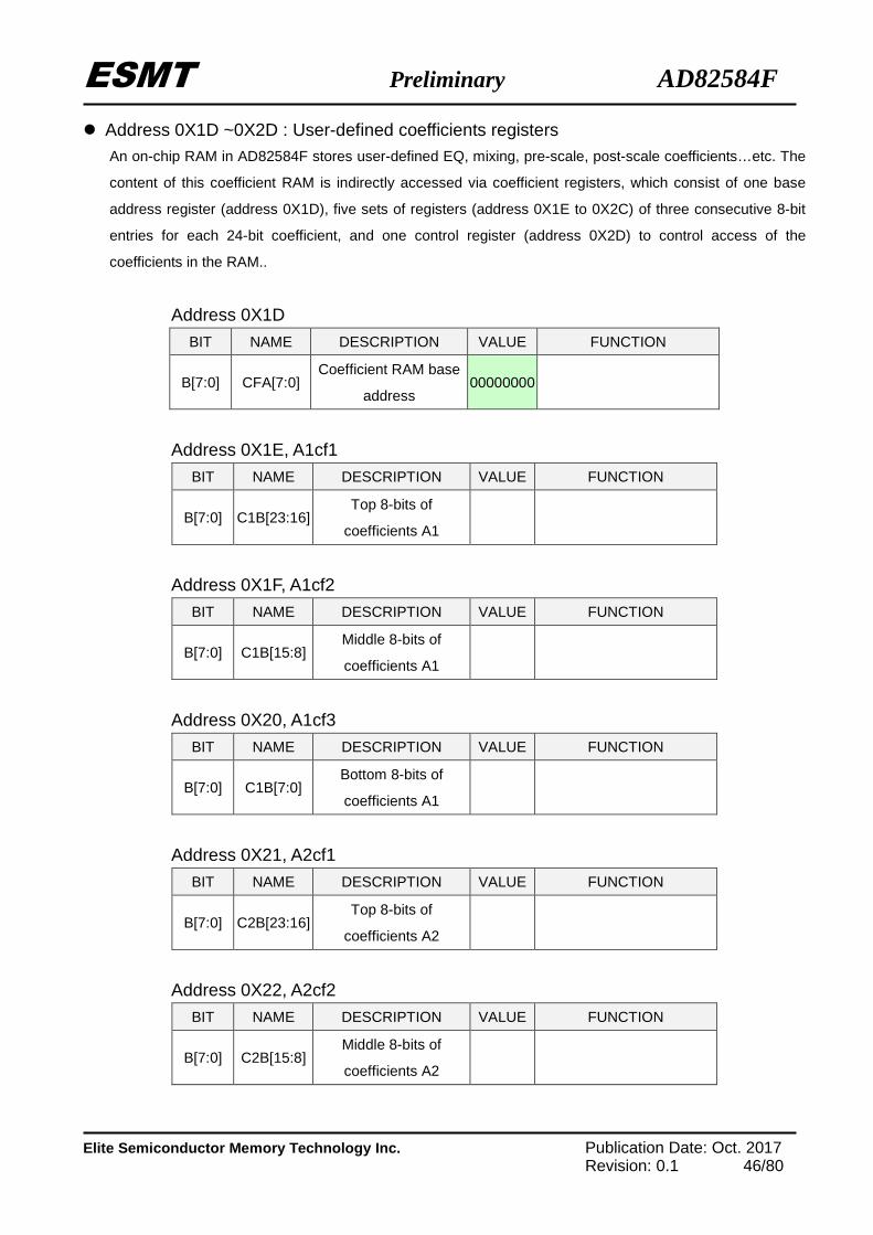
Address 0X1D ~0X2D : User-defined coefficients registers An on-chip RAM in AD82584F stores user-defined EQ, mixing, pre-scale, post-scale coefficients…etc. The
content of this coefficient RAM is indirectly accessed via coefficient registers, which consist of one base
address register (address 0X1D), five sets of registers (address 0X1E to 0X2C) of three consecutive 8-bit
entries for each 24-bit coefficient, and one control register (address 0X2D) to control access of the
coefficients in the RAM..
Address 0X1D
BIT NAME DESCRIPTION VALUE FUNCTION
B[7:0] CFA[7:0] Coefficient RAM base
address 00000000
Address 0X1E, A1cf1
BIT NAME DESCRIPTION VALUE FUNCTION
B[7:0] C1B[23:16] Top 8-bits of
coefficients A1
Address 0X1F, A1cf2
BIT NAME DESCRIPTION VALUE FUNCTION
B[7:0] C1B[15:8] Middle 8-bits of
coefficients A1
Address 0X20, A1cf3
BIT NAME DESCRIPTION VALUE FUNCTION
B[7:0] C1B[7:0] Bottom 8-bits of
coefficients A1
Address 0X21, A2cf1
BIT NAME DESCRIPTION VALUE FUNCTION
B[7:0] C2B[23:16] Top 8-bits of
coefficients A2
Address 0X22, A2cf2
BIT NAME DESCRIPTION VALUE FUNCTION
B[7:0] C2B[15:8] Middle 8-bits of
coefficients A2
ESMT Preliminary AD82584F
Elite Semiconductor Memory Technology Inc. Publication Date: Oct. 2017 Revision: 0.1 47/80
Address 0X23, A2cf3
BIT NAME DESCRIPTION VALUE FUNCTION
B[7:0] C2B[7:0] Bottom 8-bits of
coefficients A2
Address 0X24, B1cf1
BIT NAME DESCRIPTION VALUE FUNCTION
B[7:0] C3B[23:16] Top 8-bits of
coefficients B1
Address 0X25, B1cf2
BIT NAME DESCRIPTION VALUE FUNCTION
B[7:0] C3B[15:8] Middle 8-bits of
coefficients B1
Address 0X26, B1cf3
BIT NAME DESCRIPTION VALUE FUNCTION
B[7:0] C3B[7:0] Bottom 8-bits of
coefficients B1
Address 0X27, B2cf1
BIT NAME DESCRIPTION VALUE FUNCTION
B[7:0] C4B[23:16] Top 8-bits of
coefficients B2
Address 0X28, B2cf2
BIT NAME DESCRIPTION VALUE FUNCTION
B[7:0] C4B[15:8] Middle 8-bits of
coefficients B2
Address 0X29, B2cf3
BIT NAME DESCRIPTION VALUE FUNCTION
B[7:0] C4B[7:0] Bottom 8-bits of
coefficients B2
ESMT Preliminary AD82584F
Elite Semiconductor Memory Technology Inc. Publication Date: Oct. 2017 Revision: 0.1 48/80
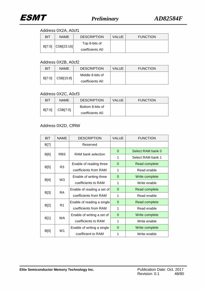
Address 0X2A, A0cf1
BIT NAME DESCRIPTION VALUE FUNCTION
B[7:0] C5B[23:16] Top 8-bits of
coefficients A0
Address 0X2B, A0cf2
BIT NAME DESCRIPTION VALUE FUNCTION
B[7:0] C5B[15:8] Middle 8-bits of
coefficients A0
Address 0X2C, A0cf3
BIT NAME DESCRIPTION VALUE FUNCTION
B[7:0] C5B[7:0] Bottom 8-bits of
coefficients A0
Address 0X2D, CfRW
BIT NAME DESCRIPTION VALUE FUNCTION
B[7] Reserved
B[6] RBS RAM bank selection 0 Select RAM bank 0
1 Select RAM bank 1
B[5] R3 Enable of reading three
coefficients from RAM
0 Read complete
1 Read enable
B[4] W3 Enable of writing three
coefficients to RAM
0 Write complete
1 Write enable
B[3] RA Enable of reading a set of
coefficients from RAM
0 Read complete
1 Read enable
B[2] R1 Enable of reading a single
coefficients from RAM
0 Read complete
1 Read enable
B[1] WA Enable of writing a set of
coefficients to RAM
0 Write complete
1 Write enable
B[0] W1 Enable of writing a single
coefficient to RAM
0 Write complete
1 Write enable
ESMT Preliminary AD82584F
Elite Semiconductor Memory Technology Inc. Publication Date: Oct. 2017 Revision: 0.1 49/80
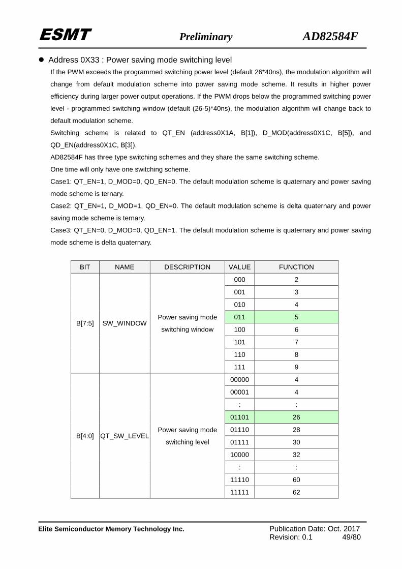
Address 0X33 : Power saving mode switching level If the PWM exceeds the programmed switching power level (default 26*40ns), the modulation algorithm will
change from default modulation scheme into power saving mode scheme. It results in higher power
efficiency during larger power output operations. If the PWM drops below the programmed switching power
level - programmed switching window (default (26-5)*40ns), the modulation algorithm will change back to
default modulation scheme.
Switching scheme is related to QT_EN (address0X1A, B[1]), D_MOD(address0X1C, B[5]), and
QD_EN(address0X1C, B[3]).
AD82584F has three type switching schemes and they share the same switching scheme.
One time will only have one switching scheme.
Case1: QT_EN=1, D_MOD=0, QD_EN=0. The default modulation scheme is quaternary and power saving
mode scheme is ternary.
Case2: QT_EN=1, D_MOD=1, QD_EN=0. The default modulation scheme is delta quaternary and power
saving mode scheme is ternary.
Case3: QT_EN=0, D_MOD=0, QD_EN=1. The default modulation scheme is quaternary and power saving
mode scheme is delta quaternary.
BIT NAME DESCRIPTION VALUE FUNCTION
B[7:5] SW_WINDOW Power saving mode
switching window
000 2
001 3
010 4
011 5
100 6
101 7
110 8
111 9
B[4:0] QT_SW_LEVEL Power saving mode
switching level
00000 4
00001 4
: :
01101 26
01110 28
01111 30
10000 32
: :
11110 60
11111 62
ESMT Preliminary AD82584F
Elite Semiconductor Memory Technology Inc. Publication Date: Oct. 2017 Revision: 0.1 50/80
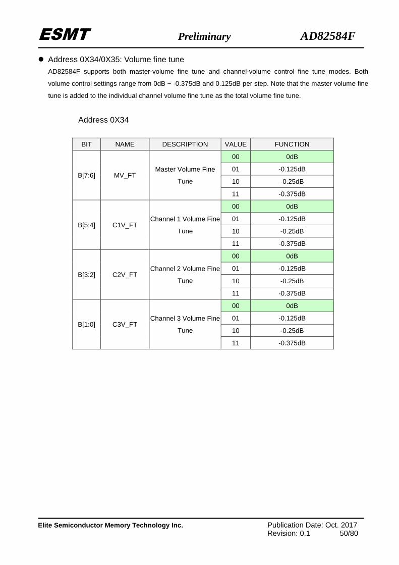
Address 0X34/0X35: Volume fine tune AD82584F supports both master-volume fine tune and channel-volume control fine tune modes. Both
volume control settings range from 0dB ~ -0.375dB and 0.125dB per step. Note that the master volume fine
tune is added to the individual channel volume fine tune as the total volume fine tune.
Address 0X34
BIT NAME DESCRIPTION VALUE FUNCTION
B[7:6] MV_FT Master Volume Fine
Tune
00 0dB
01 -0.125dB
10 -0.25dB
11 -0.375dB
B[5:4] C1V_FT Channel 1 Volume Fine
Tune
00 0dB
01 -0.125dB
10 -0.25dB
11 -0.375dB
B[3:2] C2V_FT Channel 2 Volume Fine
Tune
00 0dB
01 -0.125dB
10 -0.25dB
11 -0.375dB
B[1:0] C3V_FT Channel 3 Volume Fine
Tune
00 0dB
01 -0.125dB
10 -0.25dB
11 -0.375dB
ESMT Preliminary AD82584F
Elite Semiconductor Memory Technology Inc. Publication Date: Oct. 2017 Revision: 0.1 51/80
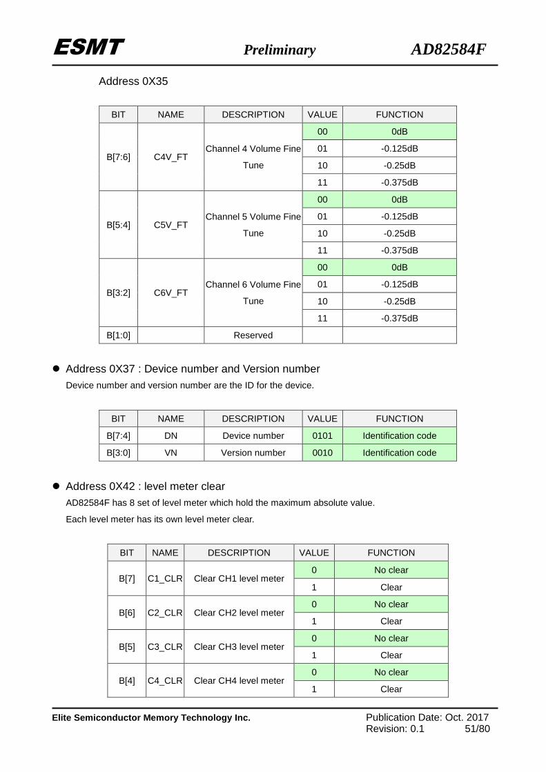
Address 0X35
BIT NAME DESCRIPTION VALUE FUNCTION
B[7:6] C4V_FT Channel 4 Volume Fine
Tune
00 0dB
01 -0.125dB
10 -0.25dB
11 -0.375dB
B[5:4] C5V_FT Channel 5 Volume Fine
Tune
00 0dB
01 -0.125dB
10 -0.25dB
11 -0.375dB
B[3:2] C6V_FT Channel 6 Volume Fine
Tune
00 0dB
01 -0.125dB
10 -0.25dB
11 -0.375dB
B[1:0] Reserved
Address 0X37 : Device number and Version number Device number and version number are the ID for the device.
BIT NAME DESCRIPTION VALUE FUNCTION
B[7:4] DN Device number 0101 Identification code
B[3:0] VN Version number 0010 Identification code
Address 0X42 : level meter clear AD82584F has 8 set of level meter which hold the maximum absolute value.
Each level meter has its own level meter clear.
BIT NAME DESCRIPTION VALUE FUNCTION
B[7] C1_CLR Clear CH1 level meter 0 No clear
1 Clear
B[6] C2_CLR Clear CH2 level meter 0 No clear
1 Clear
B[5] C3_CLR Clear CH3 level meter 0 No clear
1 Clear
B[4] C4_CLR Clear CH4 level meter 0 No clear
1 Clear
ESMT Preliminary AD82584F
Elite Semiconductor Memory Technology Inc. Publication Date: Oct. 2017 Revision: 0.1 52/80
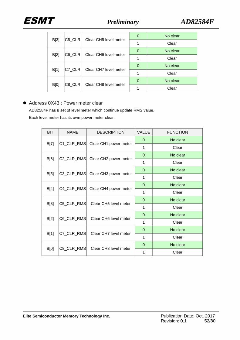
B[3] C5_CLR Clear CH5 level meter 0 No clear
1 Clear
B[2] C6_CLR Clear CH6 level meter 0 No clear
1 Clear
B[1] C7_CLR Clear CH7 level meter 0 No clear
1 Clear
B[0] C8_CLR Clear CH8 level meter 0 No clear
1 Clear
Address 0X43 : Power meter clear AD82584F has 8 set of level meter which continue update RMS value.
Each level meter has its own power meter clear.
BIT NAME DESCRIPTION VALUE FUNCTION
B[7] C1_CLR_RMS Clear CH1 power meter 0 No clear
1 Clear
B[6] C2_CLR_RMS Clear CH2 power meter 0 No clear
1 Clear
B[5] C3_CLR_RMS Clear CH3 power meter 0 No clear
1 Clear
B[4] C4_CLR_RMS Clear CH4 power meter 0 No clear
1 Clear
B[3] C5_CLR_RMS Clear CH5 level meter 0 No clear
1 Clear
B[2] C6_CLR_RMS Clear CH6 level meter 0 No clear
1 Clear
B[1] C7_CLR_RMS Clear CH7 level meter 0 No clear
1 Clear
B[0] C8_CLR_RMS Clear CH8 level meter 0 No clear
1 Clear
ESMT Preliminary AD82584F
Elite Semiconductor Memory Technology Inc. Publication Date: Oct. 2017 Revision: 0.1 53/80
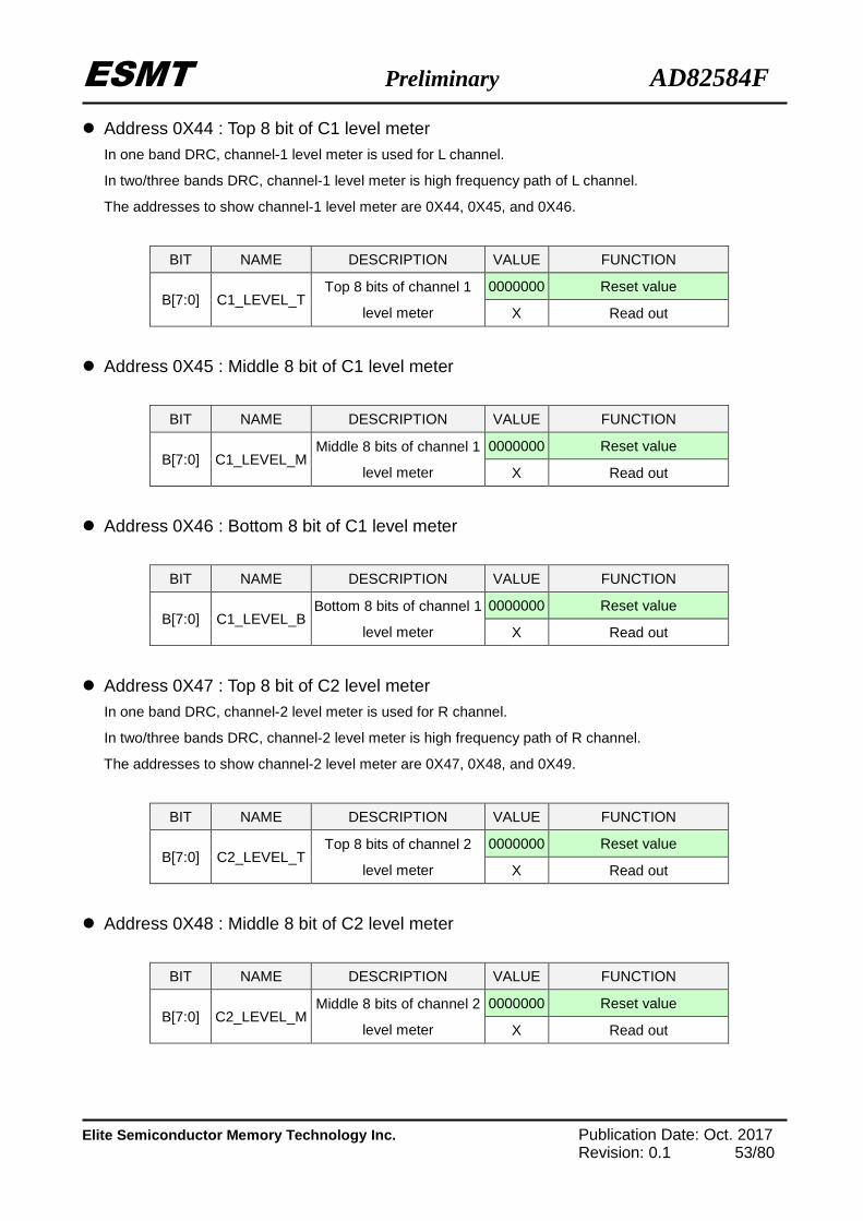
Address 0X44 : Top 8 bit of C1 level meter In one band DRC, channel-1 level meter is used for L channel.
In two/three bands DRC, channel-1 level meter is high frequency path of L channel.
The addresses to show channel-1 level meter are 0X44, 0X45, and 0X46.
BIT NAME DESCRIPTION VALUE FUNCTION
B[7:0] C1_LEVEL_T Top 8 bits of channel 1
level meter
0000000 Reset value
X Read out
Address 0X45 : Middle 8 bit of C1 level meter
BIT NAME DESCRIPTION VALUE FUNCTION
B[7:0] C1_LEVEL_M Middle 8 bits of channel 1
level meter
0000000 Reset value
X Read out
Address 0X46 : Bottom 8 bit of C1 level meter
BIT NAME DESCRIPTION VALUE FUNCTION
B[7:0] C1_LEVEL_B Bottom 8 bits of channel 1
level meter
0000000 Reset value
X Read out
Address 0X47 : Top 8 bit of C2 level meter In one band DRC, channel-2 level meter is used for R channel.
In two/three bands DRC, channel-2 level meter is high frequency path of R channel.
The addresses to show channel-2 level meter are 0X47, 0X48, and 0X49.
BIT NAME DESCRIPTION VALUE FUNCTION
B[7:0] C2_LEVEL_T Top 8 bits of channel 2
level meter
0000000 Reset value
X Read out
Address 0X48 : Middle 8 bit of C2 level meter
BIT NAME DESCRIPTION VALUE FUNCTION
B[7:0] C2_LEVEL_M Middle 8 bits of channel 2
level meter
0000000 Reset value
X Read out
ESMT Preliminary AD82584F
Elite Semiconductor Memory Technology Inc. Publication Date: Oct. 2017 Revision: 0.1 54/80
Address 0X49 : Bottom 8 bit of C2 level meter
BIT NAME DESCRIPTION VALUE FUNCTION
B[7:0] C2_LEVEL_B Bottom 8 bits of channel 2
level meter
0000000 Reset value
X Read out
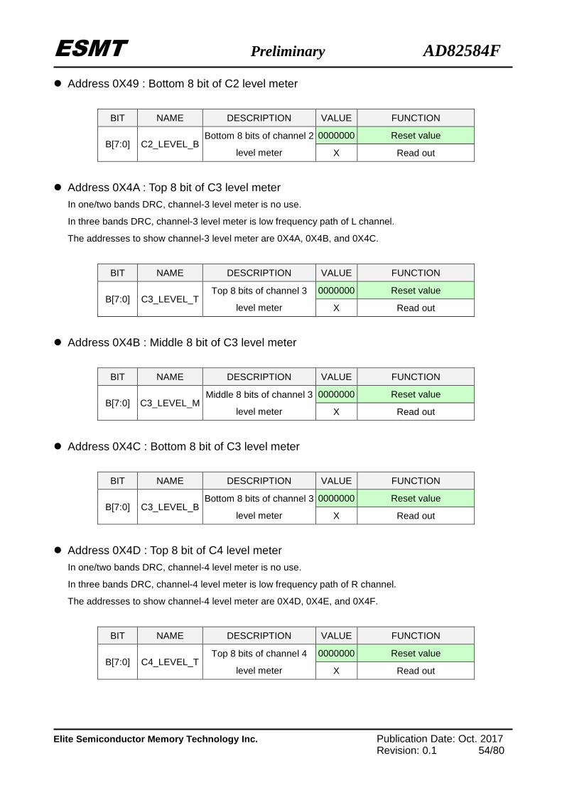
Address 0X4A : Top 8 bit of C3 level meter In one/two bands DRC, channel-3 level meter is no use.
In three bands DRC, channel-3 level meter is low frequency path of L channel.
The addresses to show channel-3 level meter are 0X4A, 0X4B, and 0X4C.
BIT NAME DESCRIPTION VALUE FUNCTION
B[7:0] C3_LEVEL_T Top 8 bits of channel 3
level meter
0000000 Reset value
X Read out
Address 0X4B : Middle 8 bit of C3 level meter
BIT NAME DESCRIPTION VALUE FUNCTION
B[7:0] C3_LEVEL_M Middle 8 bits of channel 3
level meter
0000000 Reset value
X Read out
Address 0X4C : Bottom 8 bit of C3 level meter
BIT NAME DESCRIPTION VALUE FUNCTION
B[7:0] C3_LEVEL_B Bottom 8 bits of channel 3
level meter
0000000 Reset value
X Read out
Address 0X4D : Top 8 bit of C4 level meter In one/two bands DRC, channel-4 level meter is no use.
In three bands DRC, channel-4 level meter is low frequency path of R channel.
The addresses to show channel-4 level meter are 0X4D, 0X4E, and 0X4F.
BIT NAME DESCRIPTION VALUE FUNCTION
B[7:0] C4_LEVEL_T Top 8 bits of channel 4
level meter
0000000 Reset value
X Read out
ESMT Preliminary AD82584F
Elite Semiconductor Memory Technology Inc. Publication Date: Oct. 2017 Revision: 0.1 55/80
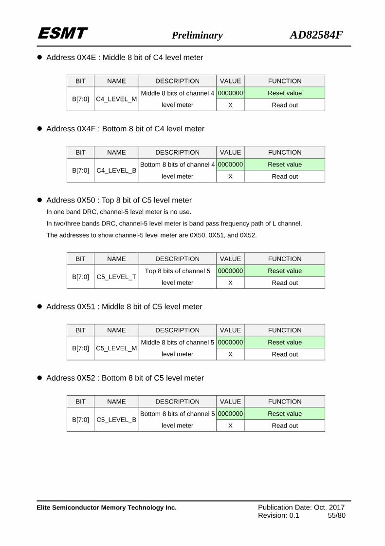
Address 0X4E : Middle 8 bit of C4 level meter
BIT NAME DESCRIPTION VALUE FUNCTION
B[7:0] C4_LEVEL_M Middle 8 bits of channel 4
level meter
0000000 Reset value
X Read out
Address 0X4F : Bottom 8 bit of C4 level meter
BIT NAME DESCRIPTION VALUE FUNCTION
B[7:0] C4_LEVEL_B Bottom 8 bits of channel 4
level meter
0000000 Reset value
X Read out
Address 0X50 : Top 8 bit of C5 level meter In one band DRC, channel-5 level meter is no use.
In two/three bands DRC, channel-5 level meter is band pass frequency path of L channel.
The addresses to show channel-5 level meter are 0X50, 0X51, and 0X52.
BIT NAME DESCRIPTION VALUE FUNCTION
B[7:0] C5_LEVEL_T Top 8 bits of channel 5
level meter
0000000 Reset value
X Read out
Address 0X51 : Middle 8 bit of C5 level meter
BIT NAME DESCRIPTION VALUE FUNCTION
B[7:0] C5_LEVEL_M Middle 8 bits of channel 5
level meter
0000000 Reset value
X Read out
Address 0X52 : Bottom 8 bit of C5 level meter
BIT NAME DESCRIPTION VALUE FUNCTION
B[7:0] C5_LEVEL_B Bottom 8 bits of channel 5
level meter
0000000 Reset value
X Read out
ESMT Preliminary AD82584F
Elite Semiconductor Memory Technology Inc. Publication Date: Oct. 2017 Revision: 0.1 56/80
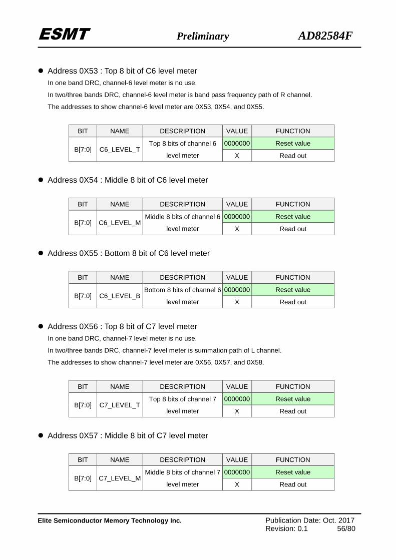
Address 0X53 : Top 8 bit of C6 level meter In one band DRC, channel-6 level meter is no use.
In two/three bands DRC, channel-6 level meter is band pass frequency path of R channel.
The addresses to show channel-6 level meter are 0X53, 0X54, and 0X55.
BIT NAME DESCRIPTION VALUE FUNCTION
B[7:0] C6_LEVEL_T Top 8 bits of channel 6
level meter
0000000 Reset value
X Read out
Address 0X54 : Middle 8 bit of C6 level meter
BIT NAME DESCRIPTION VALUE FUNCTION
B[7:0] C6_LEVEL_M Middle 8 bits of channel 6
level meter
0000000 Reset value
X Read out
Address 0X55 : Bottom 8 bit of C6 level meter
BIT NAME DESCRIPTION VALUE FUNCTION
B[7:0] C6_LEVEL_B Bottom 8 bits of channel 6
level meter
0000000 Reset value
X Read out
Address 0X56 : Top 8 bit of C7 level meter In one band DRC, channel-7 level meter is no use.
In two/three bands DRC, channel-7 level meter is summation path of L channel.
The addresses to show channel-7 level meter are 0X56, 0X57, and 0X58.
BIT NAME DESCRIPTION VALUE FUNCTION
B[7:0] C7_LEVEL_T Top 8 bits of channel 7
level meter
0000000 Reset value
X Read out
Address 0X57 : Middle 8 bit of C7 level meter
BIT NAME DESCRIPTION VALUE FUNCTION
B[7:0] C7_LEVEL_M Middle 8 bits of channel 7
level meter
0000000 Reset value
X Read out
ESMT Preliminary AD82584F
Elite Semiconductor Memory Technology Inc. Publication Date: Oct. 2017 Revision: 0.1 57/80
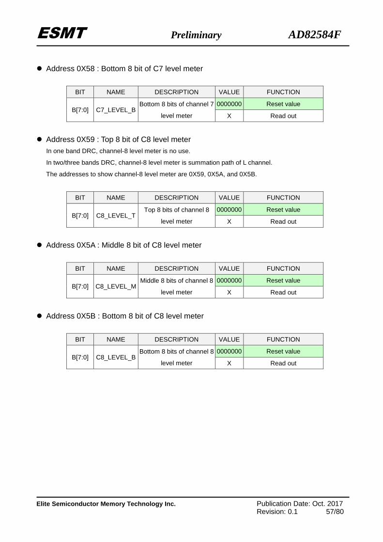
Address 0X58 : Bottom 8 bit of C7 level meter
BIT NAME DESCRIPTION VALUE FUNCTION
B[7:0] C7_LEVEL_B Bottom 8 bits of channel 7
level meter
0000000 Reset value
X Read out
Address 0X59 : Top 8 bit of C8 level meter In one band DRC, channel-8 level meter is no use.
In two/three bands DRC, channel-8 level meter is summation path of L channel.
The addresses to show channel-8 level meter are 0X59, 0X5A, and 0X5B.
BIT NAME DESCRIPTION VALUE FUNCTION
B[7:0] C8_LEVEL_T Top 8 bits of channel 8
level meter
0000000 Reset value
X Read out
Address 0X5A : Middle 8 bit of C8 level meter
BIT NAME DESCRIPTION VALUE FUNCTION
B[7:0] C8_LEVEL_M Middle 8 bits of channel 8
level meter
0000000 Reset value
X Read out
Address 0X5B : Bottom 8 bit of C8 level meter
BIT NAME DESCRIPTION VALUE FUNCTION
B[7:0] C8_LEVEL_B Bottom 8 bits of channel 8
level meter
0000000 Reset value
X Read out
ESMT Preliminary AD82584F
Elite Semiconductor Memory Technology Inc. Publication Date: Oct. 2017 Revision: 0.1 58/80
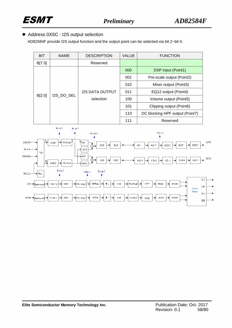
Address 0X5C : I2S output selection AD82584F provide I2S output function and the output point can be selected via bit 2~bit 0.
BIT NAME DESCRIPTION VALUE FUNCTION
B[7:3] Reserved
B[2:0] I2S_DO_SEL I2S DATA OUTPUT
selection
000 DSP input (Point1)
001 Pre-scale output (Point2)
010 Mixer output (Point3)
011 EQ12 output (Point4)
100 Volume output (Point5)
101 Clipping output (Point6)
110 DC blocking HPF output (Point7)
111 Reserved
ESMT Preliminary AD82584F
Elite Semiconductor Memory Technology Inc. Publication Date: Oct. 2017 Revision: 0.1 59/80
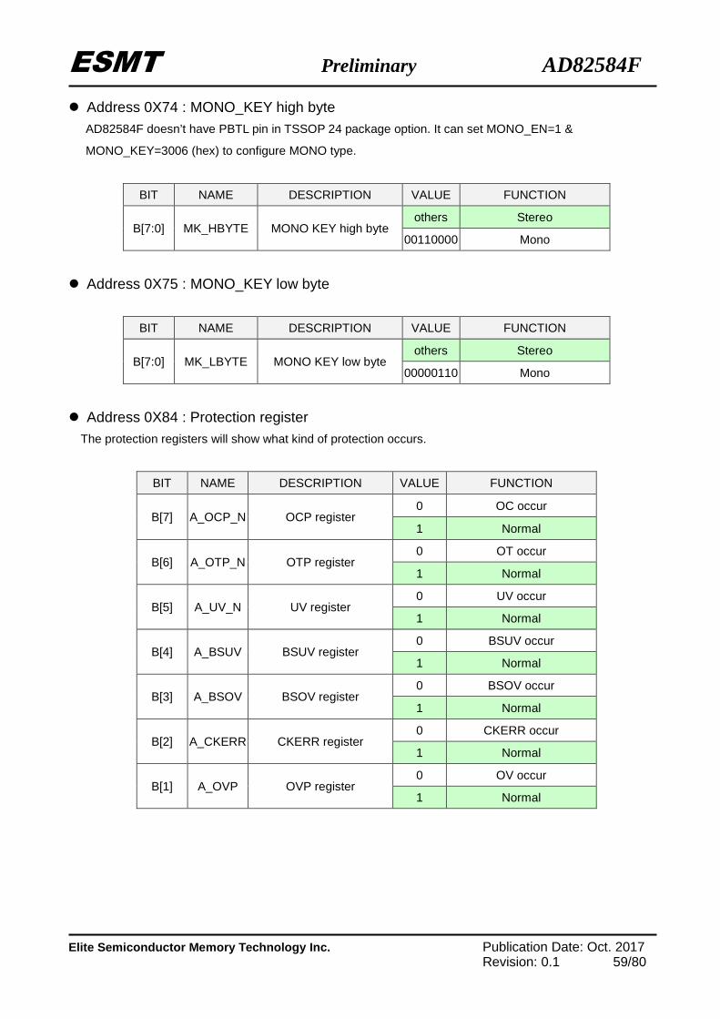
Address 0X74 : MONO_KEY high byte AD82584F doesn’t have PBTL pin in TSSOP 24 package option. It can set MONO_EN=1 &
MONO_KEY=3006 (hex) to configure MONO type.
BIT NAME DESCRIPTION VALUE FUNCTION
B[7:0] MK_HBYTE MONO KEY high byte others Stereo
00110000 Mono
Address 0X75 : MONO_KEY low byte
BIT NAME DESCRIPTION VALUE FUNCTION
B[7:0] MK_LBYTE MONO KEY low byte others Stereo
00000110 Mono
Address 0X84 : Protection register The protection registers will show what kind of protection occurs.
BIT NAME DESCRIPTION VALUE FUNCTION
B[7] A_OCP_N OCP register 0 OC occur
1 Normal
B[6] A_OTP_N OTP register 0 OT occur
1 Normal
B[5] A_UV_N UV register 0 UV occur
1 Normal
B[4] A_BSUV BSUV register 0 BSUV occur
1 Normal
B[3] A_BSOV BSOV register 0 BSOV occur
1 Normal
B[2] A_CKERR CKERR register 0 CKERR occur
1 Normal
B[1] A_OVP OVP register 0 OV occur
1 Normal
ESMT Preliminary AD82584F
Elite Semiconductor Memory Technology Inc. Publication Date: Oct. 2017 Revision: 0.1 60/80
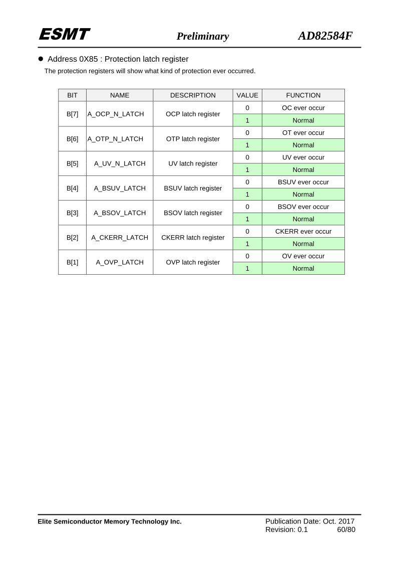
Address 0X85 : Protection latch register The protection registers will show what kind of protection ever occurred.
BIT NAME DESCRIPTION VALUE FUNCTION
B[7] A_OCP_N_LATCH OCP latch register 0 OC ever occur
1 Normal
B[6] A_OTP_N_LATCH OTP latch register 0 OT ever occur
1 Normal
B[5] A_UV_N_LATCH UV latch register 0 UV ever occur
1 Normal
B[4] A_BSUV_LATCH BSUV latch register 0 BSUV ever occur
1 Normal
B[3] A_BSOV_LATCH BSOV latch register 0 BSOV ever occur
1 Normal
B[2] A_CKERR_LATCH CKERR latch register 0 CKERR ever occur
1 Normal
B[1] A_OVP_LATCH OVP latch register 0 OV ever occur
1 Normal
ESMT Preliminary AD82584F
Elite Semiconductor Memory Technology Inc. Publication Date: Oct. 2017 Revision: 0.1 61/80
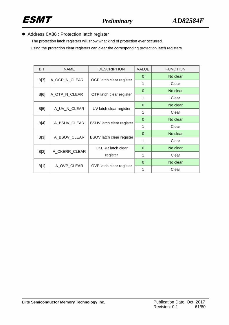
Address 0X86 : Protection latch register The protection latch registers will show what kind of protection ever occurred.
Using the protection clear registers can clear the corresponding protection latch registers.
BIT NAME DESCRIPTION VALUE FUNCTION
B[7] A_OCP_N_CLEAR OCP latch clear register 0 No clear
1 Clear
B[6] A_OTP_N_CLEAR OTP latch clear register 0 No clear
1 Clear
B[5] A_UV_N_CLEAR UV latch clear register 0 No clear
1 Clear
B[4] A_BSUV_CLEAR BSUV latch clear register 0 No clear
1 Clear
B[3] A_BSOV_CLEAR BSOV latch clear register 0 No clear
1 Clear
B[2] A_CKERR_CLEAR CKERR latch clear
register
0 No clear
1 Clear
B[1] A_OVP_CLEAR OVP latch clear register 0 No clear
1 Clear
ESMT Preliminary AD82584F
Elite Semiconductor Memory Technology Inc. Publication Date: Oct. 2017 Revision: 0.1 62/80
RAM access The procedure to read/write coefficient(s) from/to RAM is as followings:
Read a single coefficient from RAM:
1. Write 7-bis of address to I2C address-0X1D
2. Write 1 to R1 bit and write 1/0 to RBS in address-0X2D
3. Read top 8-bits of coefficient in I2C address-0X1E
4. Read middle 8-bits of coefficient in I2C address-0X1F
5. Read bottom 8-bits of coefficient in I2C address-0X20
Read a set of coefficients from RAM:
1. Write 7-bits of address to I2C address-0X1D
2. Write 1 to RA bit and write 1/0 to RBS in address-0X2D
3. Read top 8-bits of coefficient A1 in I2C address-0X1E
4. Read middle 8-bits of coefficient A1in I2C address-0X1F
5. Read bottom 8-bits of coefficient A1 in I2C address-0X20
6. Read top 8-bits of coefficient A2 in I2C address-0X21
7. Read middle 8-bits of coefficient A2 in I2C address-0X22
8. Read bottom 8-bits of coefficient A2 in I2C address-0X23
9. Read top 8-bits of coefficient B1 in I2C address-0X24
10. Read middle 8-bits of coefficient B1 in I2C address-0X25
11. Read bottom 8-bits of coefficient B1 in I2C address-0X26
12. Read top 8-bits of coefficient B2 in I2C address-0X27
13. Read middle 8-bits of coefficient B2 in I2C address-0X28
14. Read bottom 8-bits of coefficient B2 in I2C address-0X29
15. Read top 8-bits of coefficient A0 in I2C address-0X2A
16. Read middle 8-bits of coefficient A0 in I2C address-0X2B
17. Read bottom 8-bits of coefficient A0 in I2C address-0X2C
ESMT Preliminary AD82584F
Elite Semiconductor Memory Technology Inc. Publication Date: Oct. 2017 Revision: 0.1 63/80
Write a single coefficient from RAM:
1. Write 7-bis of address to I2C address-0X1D
2. Write top 8-bits of coefficient in I2C address-0X1E
3. Write middle 8-bits of coefficient in I2C address-0X1F
4. Write bottom 8-bits of coefficient in I2C address-0X20
5. Write 1 to W1 bit and write 1/0 to RBS in address-0X2D
Write a set of coefficients from RAM:
1. Write 7-bits of address to I2C address-0X1D
2. Write top 8-bits of coefficient A1 in I2C address-0X1E
3. Write middle 8-bits of coefficient A1 in I2C address-0X1F
4. Write bottom 8-bits of coefficient A1 in I2C address-0X20
5. Write top 8-bits of coefficient A2 in I2C address-0X21
6. Write middle 8-bits of coefficient A2 in I2C address-0X22
7. Write bottom 8-bits of coefficient A2 in I2C address-0X23
8. Write top 8-bits of coefficient B1 in I2C address-0X24
9. Write middle 8-bits of coefficient B1 in I2C address-0X25
10. Write bottom 8-bits of coefficient B1 in I2C address-0X26
11. Write top 8-bits of coefficient B2 in I2C address-0X27
12. Write middle 8-bits of coefficient B2 in I2C address-0X28
13. Write bottom 8-bits of coefficient B2 in I2C address-0X29
14. Write top 8-bits of coefficient A0 in I2C address-0X2A
15. Write middle 8-bits of coefficient A0 in I2C address-0X2B
16. Write bottom 8-bits of coefficient A0 in I2C address-0X2C
17. Write 1 to WA bit and write 1/0 to RBS in address-0X2D
Note that: the read and write operation on RAM coefficients works only if LRCIN (pin-15) switching on rising
edge. And, before each writing operation, it is necessary to read the address-0X24 to confirm whether RAM
is writable current in first. If the logic of W1 or WA is high, the coefficient writing is prohibited.
ESMT Preliminary AD82584F
Elite Semiconductor Memory Technology Inc. Publication Date: Oct. 2017 Revision: 0.1 64/80
User-defined equalizer The AD82584F provides 30 parametric Equalizer (EQ). User can program suitable coefficients via I2C
control interface to program the required audio band frequency response for every EQ. The transfer function
The data format of 2’s complement binary code for EQ coefficient is 3.21. i.e., 3-bits for integer (MSB is the
sign bit) and 21-bits for mantissa. Each coefficient range is from 0x800000 (-4) to 0x7FFFFF
(+3.999999523). These coefficients are stored in User Defined RAM and are referenced in following
manner:
Where x and y represents the number of channel and the band number of EQ biquard.
All user-defined filters are path-through, where all coefficients are defaulted to 0 after being powered up,
except the A0 that is set to 0x200000 which represents 1.
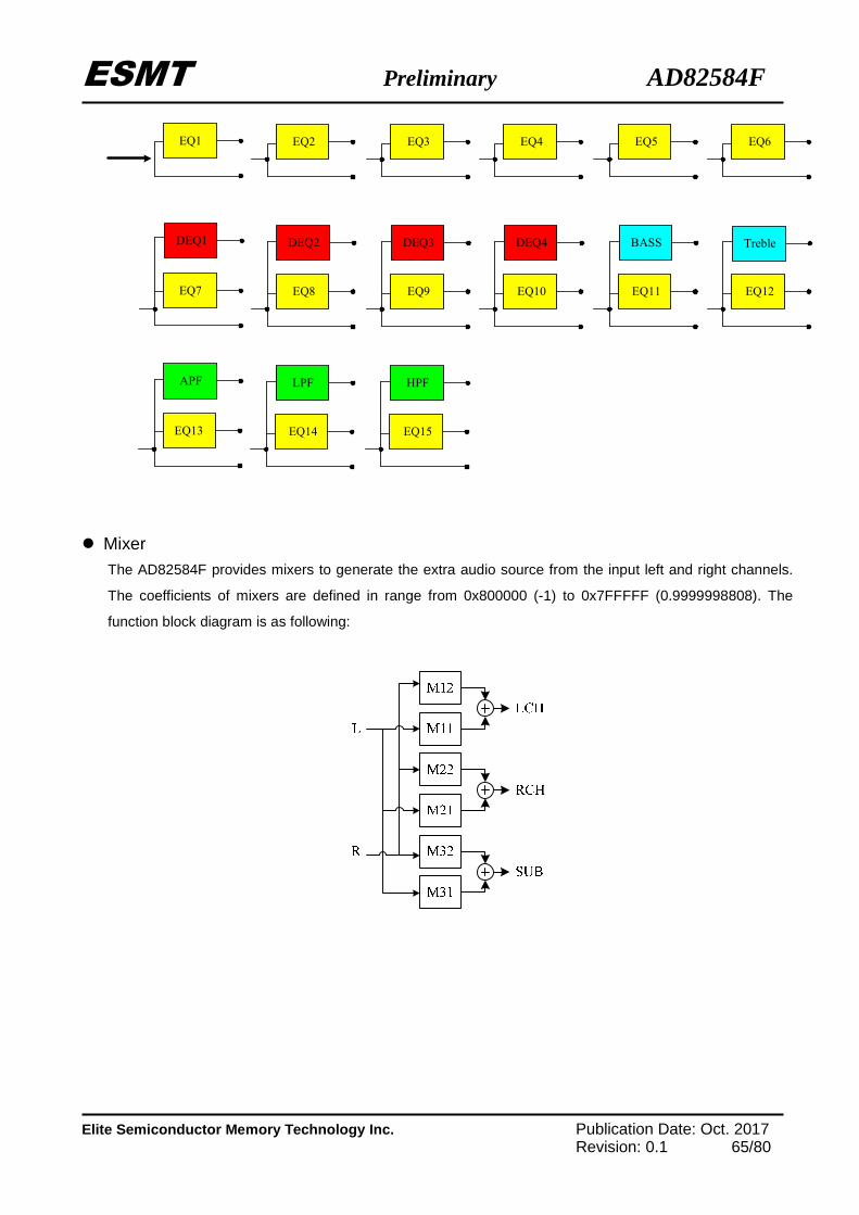
EQ arrangement AD82584F provide 15 EQ per channel.
When, register with address-0X0C, bit-5, DEQE is set to high, the EQ-7, EQ-8, EQ9, and EQ10 will use
another filter coefficient stored in used defined RAM 0X68~0X7B.
When, register with address-0X0C, bit-6, BTE is set to high, the EQ-11 and EQ-12 will perform as bass and
treble respectively.
When three bands DRC enable, EQ-13, EQ-14, and EQ-15 will perform as APF, LPF, and HPF respectively.
22
11
22
110
1)( −−
−−
++++
=zBzB
zAzAAzH
22
11
22
11
00
BCHxEQyB
BCHxEQyB
ACHxEQyA
ACHxEQyA
ACHxEQyA
−=−=
===
ESMT Preliminary AD82584F
Elite Semiconductor Memory Technology Inc. Publication Date: Oct. 2017 Revision: 0.1 65/80
EQ1 EQ2 EQ3 EQ4 EQ5 EQ6
EQ7 EQ8 EQ9 EQ10 EQ11 EQ12
DEQ1 DEQ2 DEQ3 DEQ4
EQ13 EQ14 EQ15
APF LPF HPF
BASS Treble
Mixer The AD82584F provides mixers to generate the extra audio source from the input left and right channels.
The coefficients of mixers are defined in range from 0x800000 (-1) to 0x7FFFFF (0.9999998808). The
function block diagram is as following:
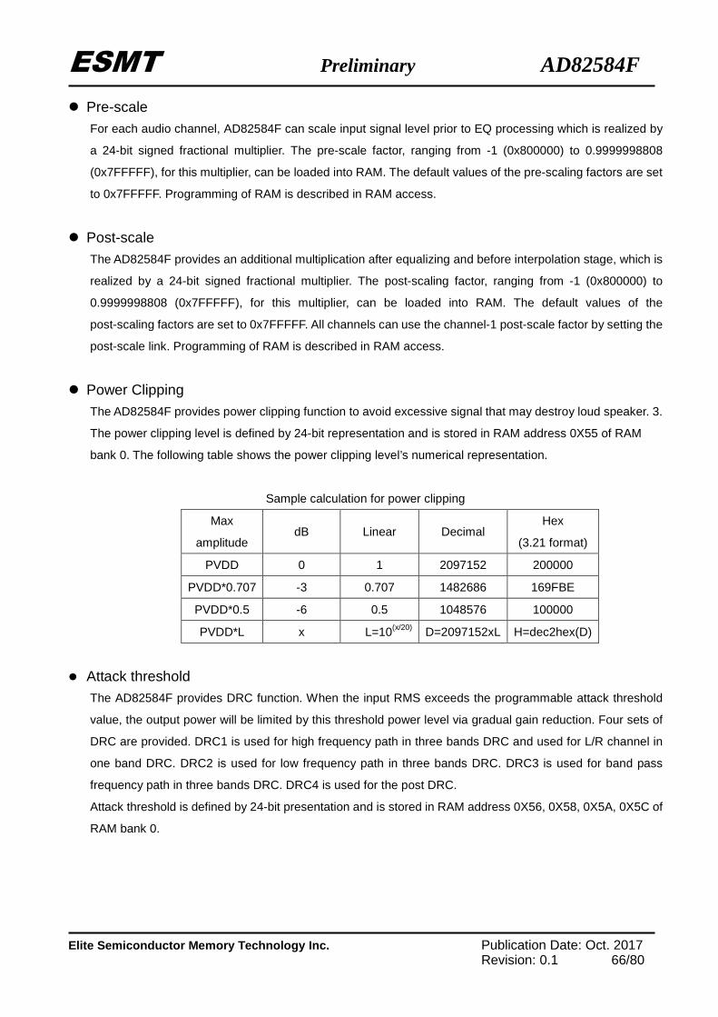
ESMT Preliminary AD82584F
Elite Semiconductor Memory Technology Inc. Publication Date: Oct. 2017 Revision: 0.1 66/80
Pre-scale For each audio channel, AD82584F can scale input signal level prior to EQ processing which is realized by
a 24-bit signed fractional multiplier. The pre-scale factor, ranging from -1 (0x800000) to 0.9999998808
(0x7FFFFF), for this multiplier, can be loaded into RAM. The default values of the pre-scaling factors are set
to 0x7FFFFF. Programming of RAM is described in RAM access.
Post-scale The AD82584F provides an additional multiplication after equalizing and before interpolation stage, which is
realized by a 24-bit signed fractional multiplier. The post-scaling factor, ranging from -1 (0x800000) to
0.9999998808 (0x7FFFFF), for this multiplier, can be loaded into RAM. The default values of the
post-scaling factors are set to 0x7FFFFF. All channels can use the channel-1 post-scale factor by setting the
post-scale link. Programming of RAM is described in RAM access.
Power Clipping The AD82584F provides power clipping function to avoid excessive signal that may destroy loud speaker. 3.
The power clipping level is defined by 24-bit representation and is stored in RAM address 0X55 of RAM
bank 0. The following table shows the power clipping level’s numerical representation.
Sample calculation for power clipping
Max
amplitude dB Linear Decimal
Hex
(3.21 format)
PVDD 0 1 2097152 200000
PVDD*0.707 -3 0.707 1482686 169FBE
PVDD*0.5 -6 0.5 1048576 100000
PVDD*L x L=10(x/20) D=2097152xL H=dec2hex(D)
Attack threshold
The AD82584F provides DRC function. When the input RMS exceeds the programmable attack threshold
value, the output power will be limited by this threshold power level via gradual gain reduction. Four sets of
DRC are provided. DRC1 is used for high frequency path in three bands DRC and used for L/R channel in
one band DRC. DRC2 is used for low frequency path in three bands DRC. DRC3 is used for band pass
frequency path in three bands DRC. DRC4 is used for the post DRC.
Attack threshold is defined by 24-bit presentation and is stored in RAM address 0X56, 0X58, 0X5A, 0X5C of
RAM bank 0.
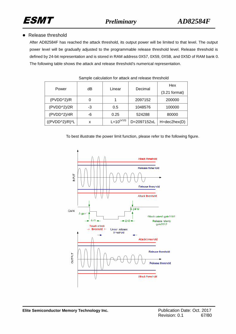
ESMT Preliminary AD82584F
Elite Semiconductor Memory Technology Inc. Publication Date: Oct. 2017 Revision: 0.1 67/80
Release threshold
After AD82584F has reached the attack threshold, its output power will be limited to that level. The output
power level will be gradually adjusted to the programmable release threshold level. Release threshold is
defined by 24-bit representation and is stored in RAM address 0X57, 0X59, 0X5B, and 0X5D of RAM bank 0.
The following table shows the attack and release threshold’s numerical representation.
Sample calculation for attack and release threshold
Power dB Linear Decimal Hex
(3.21 format)
(PVDD^2)/R 0 1 2097152 200000
(PVDD^2)/2R -3 0.5 1048576 100000
(PVDD^2)/4R -6 0.25 524288 80000
((PVDD^2)/R)*L x L=10(x/10) D=2097152xL H=dec2hex(D)
To best illustrate the power limit function, please refer to the following figure.
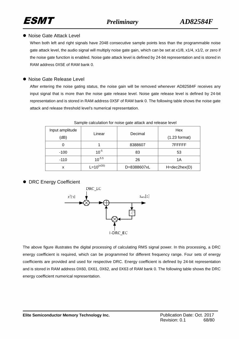
ESMT Preliminary AD82584F
Elite Semiconductor Memory Technology Inc. Publication Date: Oct. 2017 Revision: 0.1 68/80
Noise Gate Attack Level When both left and right signals have 2048 consecutive sample points less than the programmable noise
gate attack level, the audio signal will multiply noise gate gain, which can be set at x1/8, x1/4, x1/2, or zero if
the noise gate function is enabled. Noise gate attack level is defined by 24-bit representation and is stored in
RAM address 0X5E of RAM bank 0.
Noise Gate Release Level After entering the noise gating status, the noise gain will be removed whenever AD82584F receives any
input signal that is more than the noise gate release level. Noise gate release level is defined by 24-bit
representation and is stored in RAM address 0X5F of RAM bank 0. The following table shows the noise gate
attack and release threshold level’s numerical representation.
Sample calculation for noise gate attack and release level
Input amplitude
(dB) Linear Decimal
Hex
(1.23 format)
0 1 8388607 7FFFFF
-100 10-5 83 53
-110 10-5.5 26 1A
x L=10(x/20) D=8388607xL H=dec2hex(D)
DRC Energy Coefficient
The above figure illustrates the digital processing of calculating RMS signal power. In this processing, a DRC
energy coefficient is required, which can be programmed for different frequency range. Four sets of energy
coefficients are provided and used for respective DRC. Energy coefficient is defined by 24-bit representation
and is stored in RAM address 0X60, 0X61, 0X62, and 0X63 of RAM bank 0. The following table shows the DRC
energy coefficient numerical representation.
ESMT Preliminary AD82584F
Elite Semiconductor Memory Technology Inc. Publication Date: Oct. 2017 Revision: 0.1 69/80
Sample calculation for DRC energy coefficient
DRC energy
coefficient dB Linear Decimal
Hex
(1.23 format)
1 0 1 8388607 7FFFFF
1/256 -48.2 1/256 32768 8000
1/1024 -60.2 1/1024 8192 2000
L x L=10(x/20) D=8388607xL H=dec2hex(D)
The user defined RAM The contents of user defined RAM is represented in following table.
Ram Bank selection = 1
Address NAME Coefficient Default
0x00
1st SET
Channel-1 EQ1
CH1EQ1A1 0x000000
0x01 CH1EQ1A2 0x000000
0x02 CH1EQ1B1 0x000000
0x03 CH1EQ1B2 0x000000
0x04 CH1EQ1A0 0x200000
0x05
1st SET
Channel-1 EQ2
CH1EQ2A1 0x000000
0x06 CH1EQ2A2 0x000000
0x07 CH1EQ2B1 0x000000
0x08 CH1EQ2B2 0x000000
0x09 CH1EQ2A0 0x200000
0x0A
1st SET
Channel-1 EQ3
CH1EQ3A1 0x000000
0x0B CH1EQ3A2 0x000000
0x0C CH1EQ3B1 0x000000
0x0D CH1EQ3B2 0x000000
0x0E CH1EQ3A0 0x200000
0x0F
1st SET
Channel-1 EQ4
CH1EQ4A1 0x000000
0x10 CH1EQ4A2 0x000000
0x11 CH1EQ4B1 0x000000
0x12 CH1EQ4B2 0x000000
0x13 CH1EQ4A0 0x200000
0x14
1st SET
Channel-1 EQ5
CH1EQ5A1 0x000000
0x15 CH1EQ5A2 0x000000
0x16 CH1EQ5B1 0x000000
0x17 CH1EQ5B2 0x000000
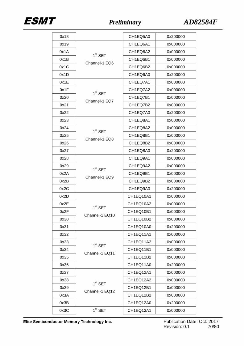
ESMT Preliminary AD82584F
Elite Semiconductor Memory Technology Inc. Publication Date: Oct. 2017 Revision: 0.1 70/80
0x18 CH1EQ5A0 0x200000
0x19
1st SET
Channel-1 EQ6
CH1EQ6A1 0x000000
0x1A CH1EQ6A2 0x000000
0x1B CH1EQ6B1 0x000000
0x1C CH1EQ6B2 0x000000
0x1D CH1EQ6A0 0x200000
0x1E
1st SET
Channel-1 EQ7
CH1EQ7A1 0x000000
0x1F CH1EQ7A2 0x000000
0x20 CH1EQ7B1 0x000000
0x21 CH1EQ7B2 0x000000
0x22 CH1EQ7A0 0x200000
0x23
1st SET
Channel-1 EQ8
CH1EQ8A1 0x000000
0x24 CH1EQ8A2 0x000000
0x25 CH1EQ8B1 0x000000
0x26 CH1EQ8B2 0x000000
0x27 CH1EQ8A0 0x200000
0x28
1st SET
Channel-1 EQ9
CH1EQ9A1 0x000000
0x29 CH1EQ9A2 0x000000
0x2A CH1EQ9B1 0x000000
0x2B CH1EQ9B2 0x000000
0x2C CH1EQ9A0 0x200000
0x2D
1st SET
Channel-1 EQ10
CH1EQ10A1 0x000000
0x2E CH1EQ10A2 0x000000
0x2F CH1EQ10B1 0x000000
0x30 CH1EQ10B2 0x000000
0x31 CH1EQ10A0 0x200000
0x32
1st SET
Channel-1 EQ11
CH1EQ11A1 0x000000
0x33 CH1EQ11A2 0x000000
0x34 CH1EQ11B1 0x000000
0x35 CH1EQ11B2 0x000000
0x36 CH1EQ11A0 0x200000
0x37
1st SET
Channel-1 EQ12
CH1EQ12A1 0x000000
0x38 CH1EQ12A2 0x000000
0x39 CH1EQ12B1 0x000000
0x3A CH1EQ12B2 0x000000
0x3B CH1EQ12A0 0x200000
0x3C 1st SET CH1EQ13A1 0x000000
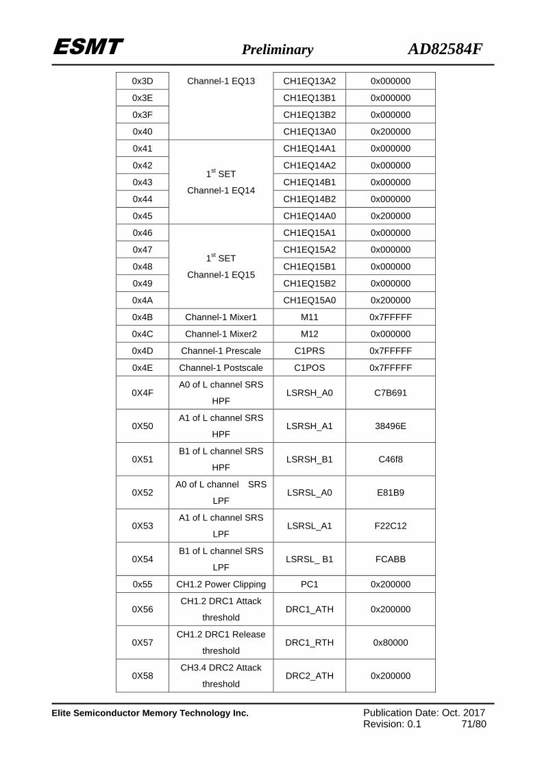
ESMT Preliminary AD82584F
Elite Semiconductor Memory Technology Inc. Publication Date: Oct. 2017 Revision: 0.1 71/80
0x3D Channel-1 EQ13 CH1EQ13A2 0x000000
0x3E CH1EQ13B1 0x000000
0x3F CH1EQ13B2 0x000000
0x40 CH1EQ13A0 0x200000
0x41
1st SET
Channel-1 EQ14
CH1EQ14A1 0x000000
0x42 CH1EQ14A2 0x000000
0x43 CH1EQ14B1 0x000000
0x44 CH1EQ14B2 0x000000
0x45 CH1EQ14A0 0x200000
0x46
1st SET
Channel-1 EQ15
CH1EQ15A1 0x000000
0x47 CH1EQ15A2 0x000000
0x48 CH1EQ15B1 0x000000
0x49 CH1EQ15B2 0x000000
0x4A CH1EQ15A0 0x200000
0x4B Channel-1 Mixer1 M11 0x7FFFFF
0x4C Channel-1 Mixer2 M12 0x000000
0x4D Channel-1 Prescale C1PRS 0x7FFFFF
0x4E Channel-1 Postscale C1POS 0x7FFFFF
0X4F A0 of L channel SRS
HPF LSRSH_A0 C7B691
0X50 A1 of L channel SRS
HPF LSRSH_A1 38496E
0X51 B1 of L channel SRS
HPF LSRSH_B1 C46f8
0X52 A0 of L channel SRS
LPF LSRSL_A0 E81B9
0X53 A1 of L channel SRS
LPF LSRSL_A1 F22C12
0X54 B1 of L channel SRS
LPF LSRSL_ B1 FCABB
0x55 CH1.2 Power Clipping PC1 0x200000
0X56 CH1.2 DRC1 Attack
threshold DRC1_ATH 0x200000
0X57 CH1.2 DRC1 Release
threshold DRC1_RTH 0x80000
0X58 CH3.4 DRC2 Attack
threshold DRC2_ATH 0x200000
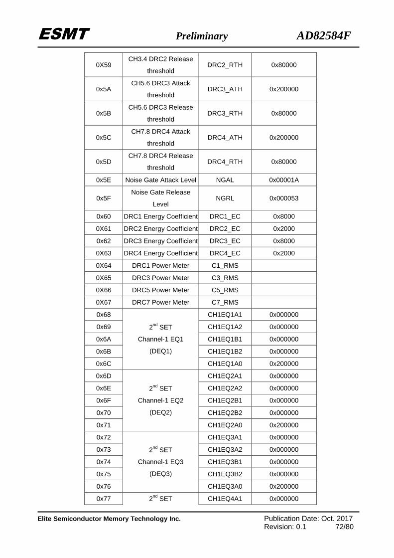
ESMT Preliminary AD82584F
Elite Semiconductor Memory Technology Inc. Publication Date: Oct. 2017 Revision: 0.1 72/80
0X59 CH3.4 DRC2 Release
threshold DRC2_RTH 0x80000
0x5A CH5.6 DRC3 Attack
threshold DRC3_ATH 0x200000
0x5B CH5.6 DRC3 Release
threshold DRC3_RTH 0x80000
0x5C CH7.8 DRC4 Attack
threshold DRC4_ATH 0x200000
0x5D CH7.8 DRC4 Release
threshold DRC4_RTH 0x80000
0x5E Noise Gate Attack Level NGAL 0x00001A
0x5F Noise Gate Release
Level NGRL 0x000053
0x60 DRC1 Energy Coefficient DRC1_EC 0x8000
0X61 DRC2 Energy Coefficient DRC2_EC 0x2000
0x62 DRC3 Energy Coefficient DRC3_EC 0x8000
0X63 DRC4 Energy Coefficient DRC4_EC 0x2000
0X64 DRC1 Power Meter C1_RMS
0X65 DRC3 Power Meter C3_RMS
0X66 DRC5 Power Meter C5_RMS
0X67 DRC7 Power Meter C7_RMS
0x68
2nd SET
Channel-1 EQ1
(DEQ1)
CH1EQ1A1 0x000000
0x69 CH1EQ1A2 0x000000
0x6A CH1EQ1B1 0x000000
0x6B CH1EQ1B2 0x000000
0x6C CH1EQ1A0 0x200000
0x6D
2nd SET
Channel-1 EQ2
(DEQ2)
CH1EQ2A1 0x000000
0x6E CH1EQ2A2 0x000000
0x6F CH1EQ2B1 0x000000
0x70 CH1EQ2B2 0x000000
0x71 CH1EQ2A0 0x200000
0x72
2nd SET
Channel-1 EQ3
(DEQ3)
CH1EQ3A1 0x000000
0x73 CH1EQ3A2 0x000000
0x74 CH1EQ3B1 0x000000
0x75 CH1EQ3B2 0x000000
0x76 CH1EQ3A0 0x200000
0x77 2nd SET CH1EQ4A1 0x000000
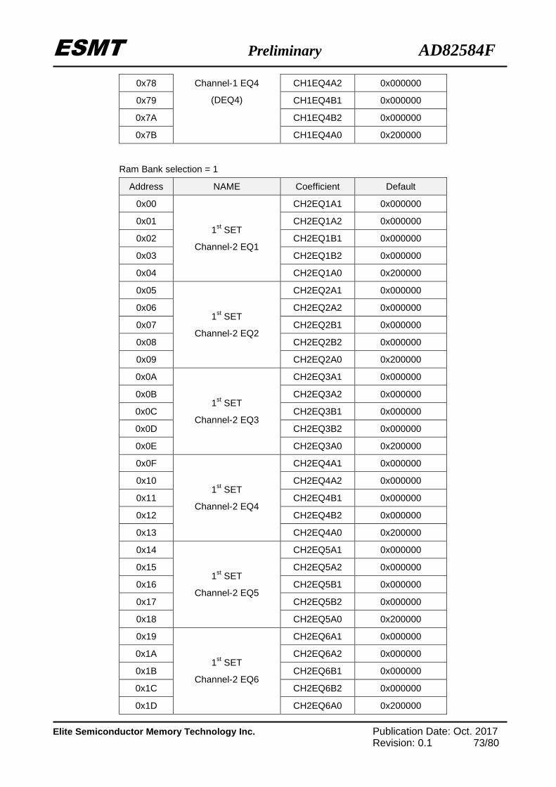
ESMT Preliminary AD82584F
Elite Semiconductor Memory Technology Inc. Publication Date: Oct. 2017 Revision: 0.1 73/80
0x78 Channel-1 EQ4
(DEQ4)
CH1EQ4A2 0x000000
0x79 CH1EQ4B1 0x000000
0x7A CH1EQ4B2 0x000000
0x7B CH1EQ4A0 0x200000
Ram Bank selection = 1
Address NAME Coefficient Default
0x00
1st SET
Channel-2 EQ1
CH2EQ1A1 0x000000
0x01 CH2EQ1A2 0x000000
0x02 CH2EQ1B1 0x000000
0x03 CH2EQ1B2 0x000000
0x04 CH2EQ1A0 0x200000
0x05
1st SET
Channel-2 EQ2
CH2EQ2A1 0x000000
0x06 CH2EQ2A2 0x000000
0x07 CH2EQ2B1 0x000000
0x08 CH2EQ2B2 0x000000
0x09 CH2EQ2A0 0x200000
0x0A
1st SET
Channel-2 EQ3
CH2EQ3A1 0x000000
0x0B CH2EQ3A2 0x000000
0x0C CH2EQ3B1 0x000000
0x0D CH2EQ3B2 0x000000
0x0E CH2EQ3A0 0x200000
0x0F
1st SET
Channel-2 EQ4
CH2EQ4A1 0x000000
0x10 CH2EQ4A2 0x000000
0x11 CH2EQ4B1 0x000000
0x12 CH2EQ4B2 0x000000
0x13 CH2EQ4A0 0x200000
0x14
1st SET
Channel-2 EQ5
CH2EQ5A1 0x000000
0x15 CH2EQ5A2 0x000000
0x16 CH2EQ5B1 0x000000
0x17 CH2EQ5B2 0x000000
0x18 CH2EQ5A0 0x200000
0x19
1st SET
Channel-2 EQ6
CH2EQ6A1 0x000000
0x1A CH2EQ6A2 0x000000
0x1B CH2EQ6B1 0x000000
0x1C CH2EQ6B2 0x000000
0x1D CH2EQ6A0 0x200000
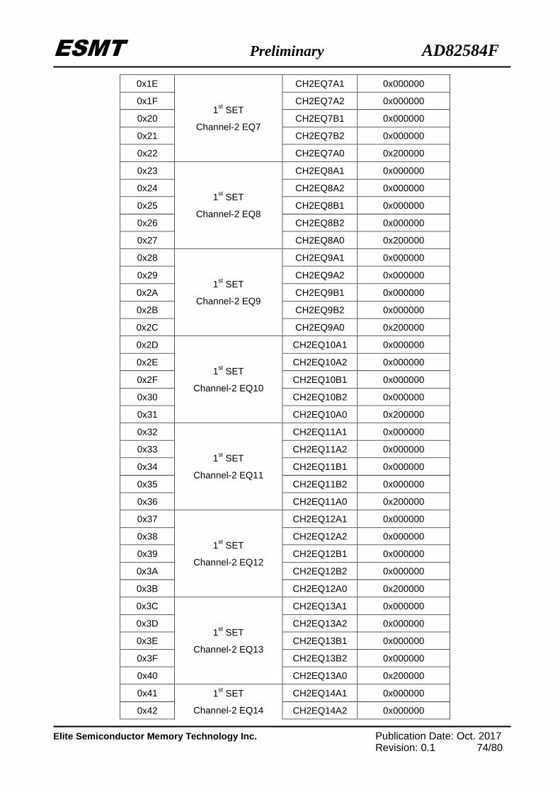
ESMT Preliminary AD82584F
Elite Semiconductor Memory Technology Inc. Publication Date: Oct. 2017 Revision: 0.1 74/80
0x1E
1st SET
Channel-2 EQ7
CH2EQ7A1 0x000000
0x1F CH2EQ7A2 0x000000
0x20 CH2EQ7B1 0x000000
0x21 CH2EQ7B2 0x000000
0x22 CH2EQ7A0 0x200000
0x23
1st SET
Channel-2 EQ8
CH2EQ8A1 0x000000
0x24 CH2EQ8A2 0x000000
0x25 CH2EQ8B1 0x000000
0x26 CH2EQ8B2 0x000000
0x27 CH2EQ8A0 0x200000
0x28
1st SET
Channel-2 EQ9
CH2EQ9A1 0x000000
0x29 CH2EQ9A2 0x000000
0x2A CH2EQ9B1 0x000000
0x2B CH2EQ9B2 0x000000
0x2C CH2EQ9A0 0x200000
0x2D
1st SET
Channel-2 EQ10
CH2EQ10A1 0x000000
0x2E CH2EQ10A2 0x000000
0x2F CH2EQ10B1 0x000000
0x30 CH2EQ10B2 0x000000
0x31 CH2EQ10A0 0x200000
0x32
1st SET
Channel-2 EQ11
CH2EQ11A1 0x000000
0x33 CH2EQ11A2 0x000000
0x34 CH2EQ11B1 0x000000
0x35 CH2EQ11B2 0x000000
0x36 CH2EQ11A0 0x200000
0x37
1st SET
Channel-2 EQ12
CH2EQ12A1 0x000000
0x38 CH2EQ12A2 0x000000
0x39 CH2EQ12B1 0x000000
0x3A CH2EQ12B2 0x000000
0x3B CH2EQ12A0 0x200000
0x3C
1st SET
Channel-2 EQ13
CH2EQ13A1 0x000000
0x3D CH2EQ13A2 0x000000
0x3E CH2EQ13B1 0x000000
0x3F CH2EQ13B2 0x000000
0x40 CH2EQ13A0 0x200000
0x41 1st SET
Channel-2 EQ14
CH2EQ14A1 0x000000
0x42 CH2EQ14A2 0x000000
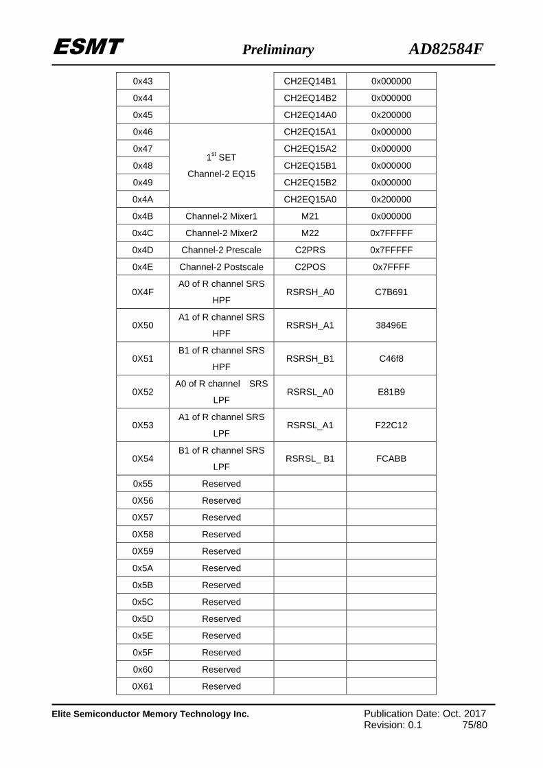
ESMT Preliminary AD82584F
Elite Semiconductor Memory Technology Inc. Publication Date: Oct. 2017 Revision: 0.1 75/80
0x43 CH2EQ14B1 0x000000
0x44 CH2EQ14B2 0x000000
0x45 CH2EQ14A0 0x200000
0x46
1st SET
Channel-2 EQ15
CH2EQ15A1 0x000000
0x47 CH2EQ15A2 0x000000
0x48 CH2EQ15B1 0x000000
0x49 CH2EQ15B2 0x000000
0x4A CH2EQ15A0 0x200000
0x4B Channel-2 Mixer1 M21 0x000000
0x4C Channel-2 Mixer2 M22 0x7FFFFF
0x4D Channel-2 Prescale C2PRS 0x7FFFFF
0x4E Channel-2 Postscale C2POS 0x7FFFF
0X4F A0 of R channel SRS
HPF RSRSH_A0 C7B691
0X50 A1 of R channel SRS
HPF RSRSH_A1 38496E
0X51 B1 of R channel SRS
HPF RSRSH_B1 C46f8
0X52 A0 of R channel SRS
LPF RSRSL_A0 E81B9
0X53 A1 of R channel SRS
LPF RSRSL_A1 F22C12
0X54 B1 of R channel SRS
LPF RSRSL_ B1 FCABB
0x55 Reserved
0X56 Reserved
0X57 Reserved
0X58 Reserved
0X59 Reserved
0x5A Reserved
0x5B Reserved
0x5C Reserved
0x5D Reserved
0x5E Reserved
0x5F Reserved
0x60 Reserved
0X61 Reserved
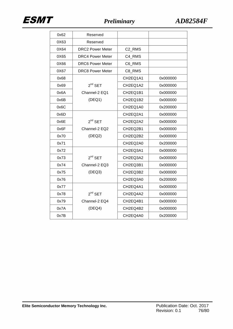
ESMT Preliminary AD82584F
Elite Semiconductor Memory Technology Inc. Publication Date: Oct. 2017 Revision: 0.1 76/80
0x62 Reserved
0X63 Reserved
0X64 DRC2 Power Meter C2_RMS
0X65 DRC4 Power Meter C4_RMS
0X66 DRC6 Power Meter C6_RMS
0X67 DRC8 Power Meter C8_RMS
0x68
2nd SET
Channel-2 EQ1
(DEQ1)
CH2EQ1A1 0x000000
0x69 CH2EQ1A2 0x000000
0x6A CH2EQ1B1 0x000000
0x6B CH2EQ1B2 0x000000
0x6C CH2EQ1A0 0x200000
0x6D
2nd SET
Channel-2 EQ2
(DEQ2)
CH2EQ2A1 0x000000
0x6E CH2EQ2A2 0x000000
0x6F CH2EQ2B1 0x000000
0x70 CH2EQ2B2 0x000000
0x71 CH2EQ2A0 0x200000
0x72
2nd SET
Channel-2 EQ3
(DEQ3)
CH2EQ3A1 0x000000
0x73 CH2EQ3A2 0x000000
0x74 CH2EQ3B1 0x000000
0x75 CH2EQ3B2 0x000000
0x76 CH2EQ3A0 0x200000
0x77
2nd SET
Channel-2 EQ4
(DEQ4)
CH2EQ4A1 0x000000
0x78 CH2EQ4A2 0x000000
0x79 CH2EQ4B1 0x000000
0x7A CH2EQ4B2 0x000000
0x7B CH2EQ4A0 0x200000
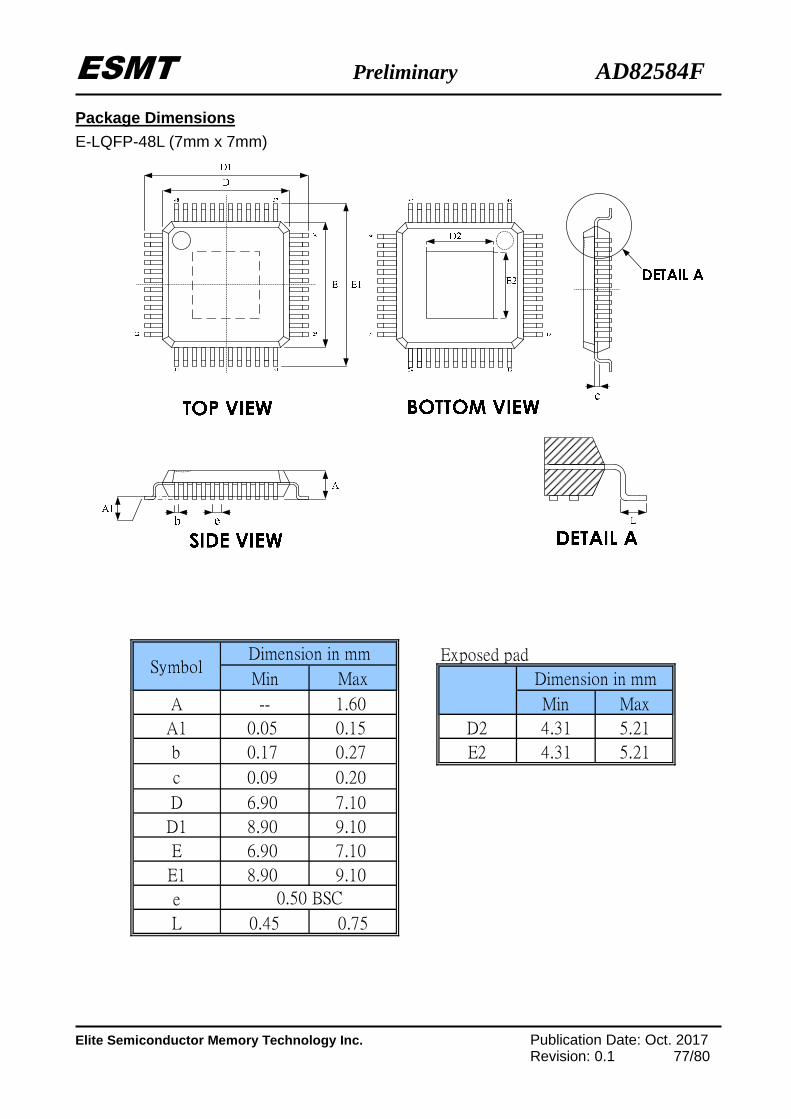
ESMT Preliminary AD82584F
Elite Semiconductor Memory Technology Inc. Publication Date: Oct. 2017 Revision: 0.1 77/80
Package Dimensions
E-LQFP-48L (7mm x 7mm)
Exposed pad
Min Max
A -- 1.60 Min Max
A1 0.05 0.15 D2 4.31 5.21
b 0.17 0.27 E2 4.31 5.21
c 0.09 0.20
D 6.90 7.10
D1 8.90 9.10
E 6.90 7.10
E1 8.90 9.10
e
L 0.45 0.75
Dimension in mmSymbol
Dimension in mm
0.50 BSC
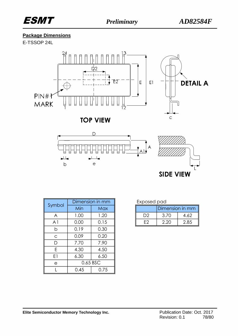
ESMT Preliminary AD82584F
Elite Semiconductor Memory Technology Inc. Publication Date: Oct. 2017 Revision: 0.1 78/80
Package Dimensions
E-TSSOP 24L
Exposed pad
Min Max Dimension in mm
A 1.00 1.20 D2 3.70 4.62
A1 0.00 0.15 E2 2.20 2.85
b 0.19 0.30
c 0.09 0.20
D 7.70 7.90
E 4.30 4.50
E1 6.30 6.50
e
L 0.45 0.75
0.65 BSC
SymbolDimension in mm
ESMT Preliminary AD82584F
Elite Semiconductor Memory Technology Inc. Publication Date: Oct. 2017 Revision: 0.1 79/80
Revision History
Revision Date Description
0.1 2017.10 Original.
ESMT Preliminary AD82584F
Elite Semiconductor Memory Technology Inc. Publication Date: Oct. 2017 Revision: 0.1 80/80
Important Notice All rights reserved. No part of this document may be reproduced or duplicated in any form or by any means without the prior permission of ESMT. The contents contained in this document are believed to be accurate at the time of publication. ESMT assumes no responsibility for any error in this document, and reserves the right to change the products or specification in this document without notice. The information contained herein is presented only as a guide or examples for the application of our products. No responsibility is assumed by ESMT for any infringement of patents, copyrights, or other intellectual property rights of third parties which may result from its use. No license, either express, implied or otherwise, is granted under any patents, copyrights or other intellectual property rights of ESMT or others. Any semiconductor devices may have inherently a certain rate of failure. To minimize risks associated with customer's application, adequate design and operating safeguards against injury, damage, or loss from such failure, should be provided by the customer when making application designs. ESMT's products are not authorized for use in critical applications such as, but not limited to, life support devices or system, where failure or abnormal operation may directly affect human lives or cause physical injury or property damage. If products described here are to be used for such kinds of application, purchaser must do its own quality assurance testing appropriate to such applications.