Embed Size (px)
Citation preview
Precision Micropower, Low Noise CMOS,Rail-to-Rail Input/Output Operational Amplifiers
AD8603/AD8607/AD8609
Rev. C Information furnished by Analog Devices is believed to be accurate and reliable. However, no responsibility is assumed by Analog Devices for its use, nor for any infringements of patents or other rights of third parties that may result from its use. Specifications subject to change without notice. No license is granted by implication or otherwise under any patent or patent rights of Analog Devices. Trademarks and registered trademarks are the property of their respective owners.
One Technology Way, P.O. Box 9106, Norwood, MA 02062-9106, U.S.A.Tel: 781.329.4700 www.analog.com Fax: 781.461.3113 ©2003–2008 Analog Devices, Inc. All rights reserved.
FEATURES Low offset voltage: 50 μV maximum Low input bias current: 1 pA maximum Single-supply operation: 1.8 V to 5 V Low noise: 22 nV/√Hz Micropower: 50 μA maximum Low distortion No phase reversal Unity gain stable
APPLICATIONS Battery-powered instrumentation Multipole filters Sensors Low power ASIC input or output amplifiers
GENERAL DESCRIPTION The AD8603/AD8607/AD8609 are single/dual/quad micro-power rail-to-rail input and output amplifiers, respectively, that feature very low offset voltage as well as low input voltage and current noise.
These amplifiers use a patented trimming technique that achieves superior precision without laser trimming. The parts are fully specified to operate from 1.8 V to 5.0 V single supply or from ±0.9 V to ±2.5 V dual supply. The combination of low offsets, low noise, very low input bias currents, and low power consumption makes the AD8603/AD8607/AD8609 especially useful in portable and loop-powered instrumentation.
The ability to swing rail to rail at both the input and output enables designers to buffer CMOS ADCs, DACs, ASICs, and other wide output swing devices in low power, single-supply systems.
The AD8603 is available in a tiny 5-lead TSOT package. The AD8607 is available in 8-lead MSOP and 8-lead SOIC packages. The AD8609 is available in 14-lead TSSOP and 14-lead SOIC packages.
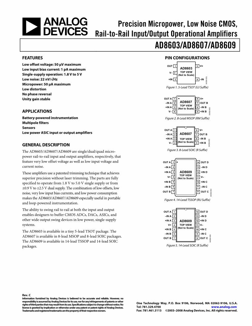
PIN CONFIGURATIONS
0435
6-00
1
OUT 1
V– 2
+IN 3
V+5
–IN4
AD8603TOP VIEW
(Not to Scale)
Figure 1. 5-Lead TSOT (UJ Suffix)
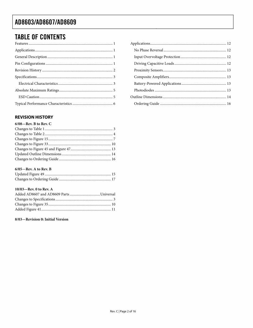
0435
6-00
2
OUT A 1
–IN A 2
+IN A 3
V– 4
V+8
OUT B7
–IN B6
+IN B5
AD8607TOP VIEW
(Not to Scale)
Figure 2. 8-Lead MSOP (RM Suffix)
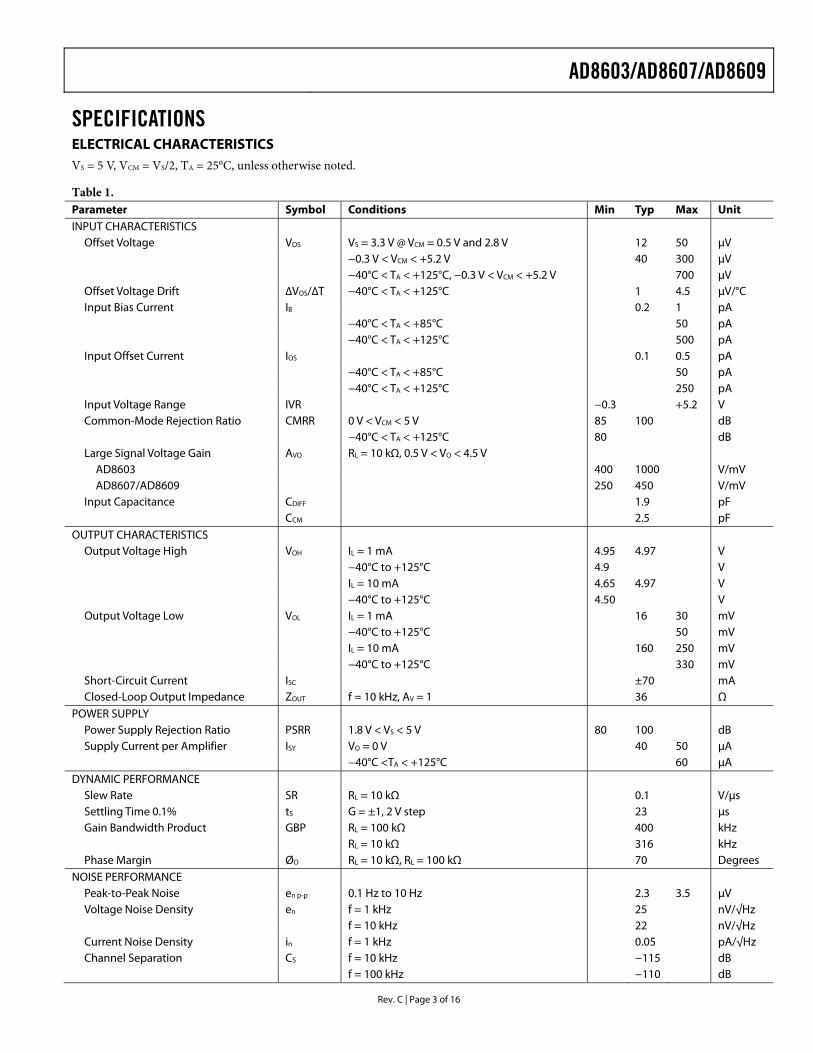
0435
6-00
3
OUT A 1
–IN A 2
+IN A 3
V– 4
V+8
OUT B7
–IN B6
+IN B5
AD8607TOP VIEW
(Not to Scale)
Figure 3. 8-Lead SOIC (R Suffix)
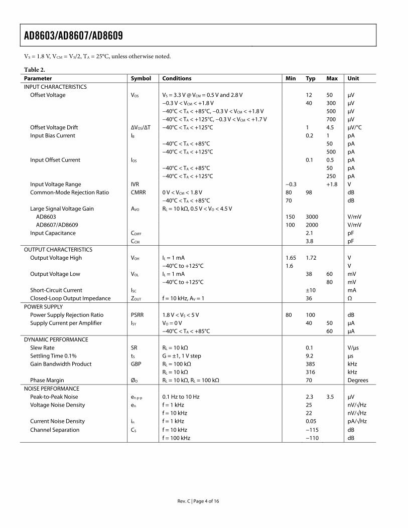
0435
6-00
4
1
2
3
4
5
6
7
AD8609–IN A
+IN A
V+
OUT B
–IN B
+IN B
OUT A 14
13
12
11
10
9
8
–IN D
+IN D
V–
OUT C
–IN C
+IN C
OUT D
TOP VIEW(Not to Scale)
Figure 4. 14-Lead TSSOP (RU Suffix)
OUT A 1
–IN A 2
+IN A 3
V+ 4
OUT D14
–IN D13
+IN D12
V–11
+IN B 5 +IN C10
–IN B 6 –IN C9
OUT B 7 OUT C8
AD8609TOP VIEW
(Not to Scale)
0435
6-00
5
Figure 5. 14-Lead SOIC (R Suffix)
AD8603/AD8607/AD8609
Rev. C | Page 2 of 16
TABLE OF CONTENTS Features .............................................................................................. 1
Applications ....................................................................................... 1
General Description ......................................................................... 1
Pin Configurations ........................................................................... 1
Revision History ............................................................................... 2
Specifications ..................................................................................... 3
Electrical Characteristics ............................................................. 3
Absolute Maximum Ratings ............................................................ 5
ESD Caution .................................................................................. 5
Typical Performance Characteristics ............................................. 6
Applications ..................................................................................... 12
No Phase Reversal ...................................................................... 12
Input Overvoltage Protection ................................................... 12
Driving Capacitive Loads .......................................................... 12
Proximity Sensors ....................................................................... 13
Composite Amplifiers ................................................................ 13
Battery-Powered Applications .................................................. 13
Photodiodes ................................................................................ 13
Outline Dimensions ....................................................................... 14
Ordering Guide .......................................................................... 16
REVISION HISTORY 6/08—Rev. B to Rev. C Changes to Table 1 ............................................................................ 3 Changes to Table 2 ............................................................................ 4 Changes to Figure 15 ........................................................................ 7 Changes to Figure 33 ...................................................................... 10 Changes to Figure 45 and Figure 47 ............................................. 13 Updated Outline Dimensions ....................................................... 14 Changes to Ordering Guide .......................................................... 16 6/05—Rev. A to Rev. B Updated Figure 49 .......................................................................... 15 Changes to Ordering Guide .......................................................... 17 10/03—Rev. 0 to Rev. A Added AD8607 and AD8609 Parts .................................. Universal Changes to Specifications ................................................................ 3 Changes to Figure 35 ...................................................................... 10 Added Figure 41 .............................................................................. 11 8/03—Revision 0: Initial Version
AD8603/AD8607/AD8609
Rev. C | Page 3 of 16
SPECIFICATIONS ELECTRICAL CHARACTERISTICS VS = 5 V, VCM = VS/2, TA = 25°C, unless otherwise noted.
Table 1. Parameter Symbol Conditions Min Typ Max Unit INPUT CHARACTERISTICS
Offset Voltage VOS VS = 3.3 V @ VCM = 0.5 V and 2.8 V 12 50 μV −0.3 V < VCM < +5.2 V 40 300 μV −40°C < TA < +125°C, −0.3 V < VCM < +5.2 V 700 μV
Offset Voltage Drift ∆VOS/∆T −40°C < TA < +125°C 1 4.5 μV/°C Input Bias Current IB 0.2 1 pA
−40°C < TA < +85°C 50 pA −40°C < TA < +125°C 500 pA
Input Offset Current IOS 0.1 0.5 pA −40°C < TA < +85°C 50 pA −40°C < TA < +125°C 250 pA
Input Voltage Range IVR −0.3 +5.2 V Common-Mode Rejection Ratio CMRR 0 V < VCM < 5 V 85 100 dB
−40°C < TA < +125°C 80 dB Large Signal Voltage Gain AVO RL = 10 kΩ, 0.5 V < VO < 4.5 V
AD8603 400 1000 V/mV AD8607/AD8609 250 450 V/mV
Input Capacitance CDIFF 1.9 pF CCM 2.5 pF OUTPUT CHARACTERISTICS
Output Voltage High VOH IL = 1 mA 4.95 4.97 V −40°C to +125°C 4.9 V IL = 10 mA 4.65 4.97 V −40°C to +125°C 4.50 V
Output Voltage Low VOL IL = 1 mA 16 30 mV −40°C to +125°C 50 mV IL = 10 mA 160 250 mV −40°C to +125°C 330 mV
Short-Circuit Current ISC ±70 mA Closed-Loop Output Impedance ZOUT f = 10 kHz, AV = 1 36 Ω
POWER SUPPLY Power Supply Rejection Ratio PSRR 1.8 V < VS < 5 V 80 100 dB Supply Current per Amplifier ISY VO = 0 V 40 50 μA
−40°C <TA < +125°C 60 μA DYNAMIC PERFORMANCE
Slew Rate SR RL = 10 kΩ 0.1 V/μs Settling Time 0.1% tS G = ±1, 2 V step 23 μs Gain Bandwidth Product GBP RL = 100 kΩ 400 kHz
RL = 10 kΩ 316 kHz Phase Margin ØO RL = 10 kΩ, RL = 100 kΩ 70 Degrees
NOISE PERFORMANCE Peak-to-Peak Noise en p-p 0.1 Hz to 10 Hz 2.3 3.5 μV Voltage Noise Density en f = 1 kHz 25 nV/√Hz
f = 10 kHz 22 nV/√Hz Current Noise Density in f = 1 kHz 0.05 pA/√Hz Channel Separation CS f = 10 kHz −115 dB f = 100 kHz −110 dB
AD8603/AD8607/AD8609
Rev. C | Page 4 of 16
VS = 1.8 V, VCM = VS/2, TA = 25°C, unless otherwise noted.
Table 2. Parameter Symbol Conditions Min Typ Max Unit INPUT CHARACTERISTICS
Offset Voltage VOS VS = 3.3 V @ VCM = 0.5 V and 2.8 V 12 50 μV −0.3 V < VCM < +1.8 V 40 300 μV −40°C < TA < +85°C, −0.3 V < VCM < +1.8 V 500 μV −40°C < TA < +125°C, −0.3 V < VCM < +1.7 V 700 μV
Offset Voltage Drift ∆VOS/∆T −40°C < TA < +125°C 1 4.5 μV/°C Input Bias Current IB 0.2 1 pA −40°C < TA < +85°C 50 pA
−40°C < TA < +125°C 500 pA Input Offset Current IOS 0.1 0.5 pA
−40°C < TA < +85°C 50 pA −40°C < TA < +125°C 250 pA
Input Voltage Range IVR −0.3 +1.8 V Common-Mode Rejection Ratio CMRR 0 V < VCM < 1.8 V 80 98 dB
−40°C < TA < +85°C 70 dB Large Signal Voltage Gain AVO RL = 10 kΩ, 0.5 V < VO < 4.5 V
AD8603 150 3000 V/mV AD8607/AD8609 100 2000 V/mV
Input Capacitance CDIFF 2.1 pF CCM 3.8 pF OUTPUT CHARACTERISTICS
Output Voltage High VOH IL = 1 mA 1.65 1.72 V −40°C to +125°C 1.6 V
Output Voltage Low VOL IL = 1 mA 38 60 mV −40°C to +125°C 80 mV
Short-Circuit Current ISC ±10 mA Closed-Loop Output Impedance ZOUT f = 10 kHz, AV = 1 36 Ω
POWER SUPPLY Power Supply Rejection Ratio PSRR 1.8 V < VS < 5 V 80 100 dB Supply Current per Amplifier ISY VO = 0 V 40 50 μA
−40°C < TA < +85°C 60 μA DYNAMIC PERFORMANCE
Slew Rate SR RL = 10 kΩ 0.1 V/μs Settling Time 0.1% tS G = ±1, 1 V step 9.2 μs Gain Bandwidth Product GBP RL = 100 kΩ 385 kHz
RL = 10 kΩ 316 kHz Phase Margin ØO RL = 10 kΩ, RL = 100 kΩ 70 Degrees
NOISE PERFORMANCE Peak-to-Peak Noise en p-p 0.1 Hz to 10 Hz 2.3 3.5 μV Voltage Noise Density en f = 1 kHz 25 nV/√Hz
f = 10 kHz 22 nV/√Hz Current Noise Density in f = 1 kHz 0.05 pA/√Hz
Channel Separation CS f = 10 kHz −115 dB f = 100 kHz −110 dB
AD8603/AD8607/AD8609
Rev. C | Page 5 of 16
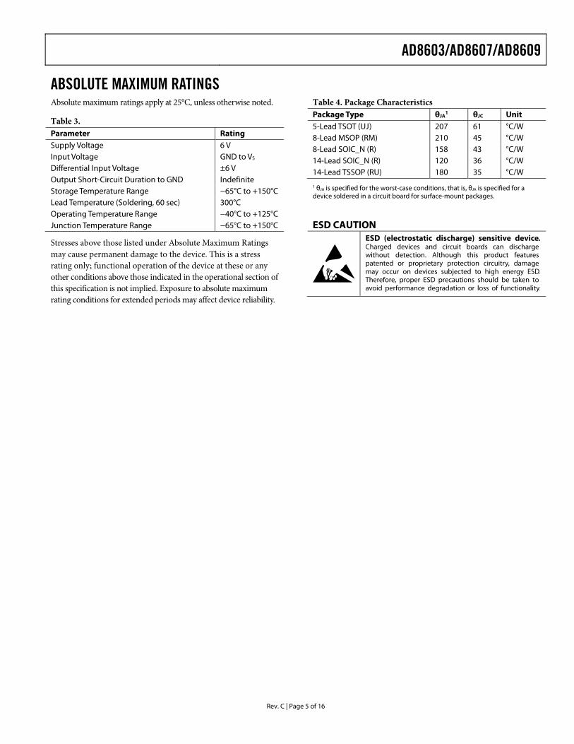
ABSOLUTE MAXIMUM RATINGS Absolute maximum ratings apply at 25°C, unless otherwise noted.
Table 3. Parameter Rating Supply Voltage 6 V Input Voltage GND to VS Differential Input Voltage ±6 V Output Short-Circuit Duration to GND Indefinite Storage Temperature Range −65°C to +150°C Lead Temperature (Soldering, 60 sec) 300°C Operating Temperature Range −40°C to +125°C Junction Temperature Range −65°C to +150°C
Stresses above those listed under Absolute Maximum Ratings may cause permanent damage to the device. This is a stress rating only; functional operation of the device at these or any other conditions above those indicated in the operational section of this specification is not implied. Exposure to absolute maximum rating conditions for extended periods may affect device reliability.
Table 4. Package Characteristics Package Type θJA
1 θJC Unit 5-Lead TSOT (UJ) 207 61 °C/W 8-Lead MSOP (RM) 210 45 °C/W 8-Lead SOIC_N (R) 158 43 °C/W 14-Lead SOIC_N (R) 120 36 °C/W 14-Lead TSSOP (RU) 180 35 °C/W
1 θJA is specified for the worst-case conditions, that is, θJA is specified for a device soldered in a circuit board for surface-mount packages.
ESD CAUTION
AD8603/AD8607/AD8609
Rev. C | Page 6 of 16
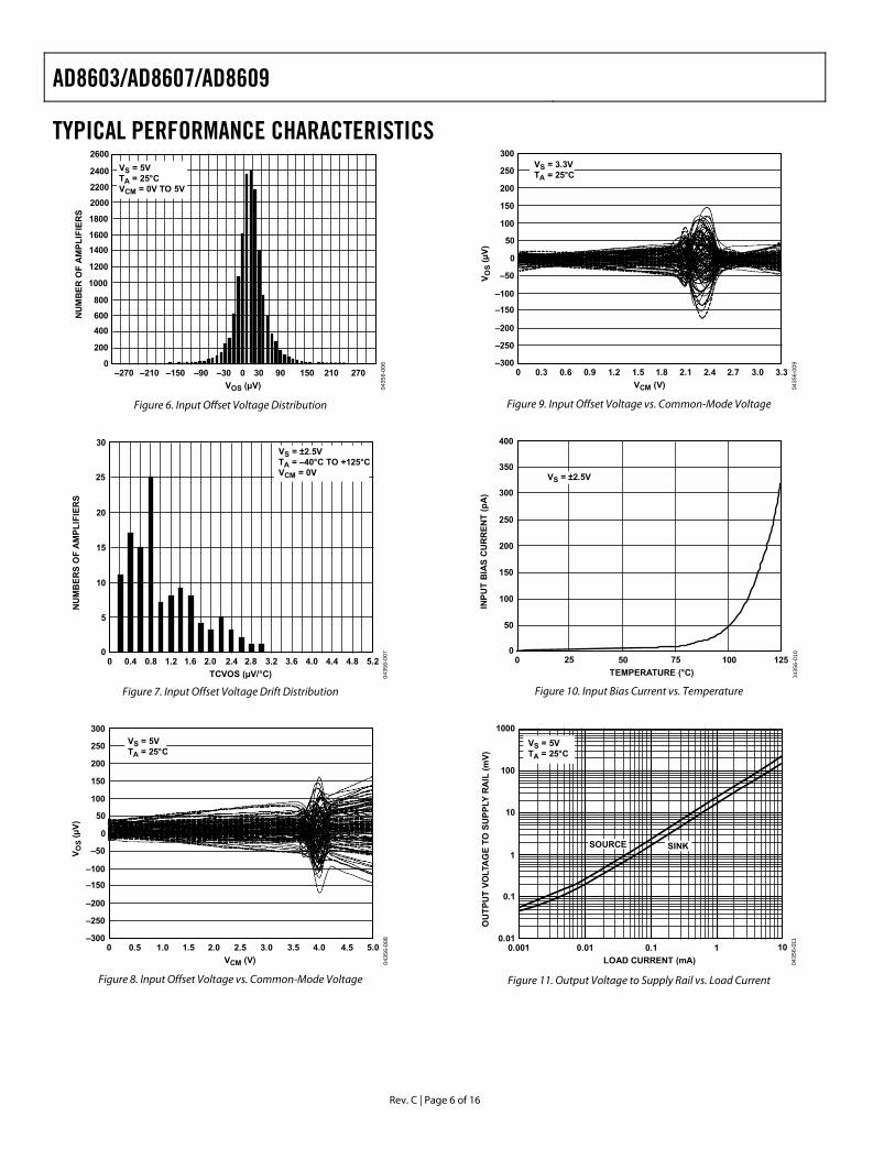
TYPICAL PERFORMANCE CHARACTERISTICS
VOS (µV)
NU
MB
ER O
FA
MPL
IFIE
RS
–2100
400
800
1200
0 150
200
600
1000
–150 –30 30 90 210 270–90
16001400
–270
1800
2000
2200
2400
2600VS = 5VTA = 25°CVCM = 0V TO 5V
0435
6-00
6
Figure 6. Input Offset Voltage Distribution
TCVOS (µV/°C)
NU
MB
ERS
OF
AM
PLIF
IER
S
00
10
20
30
1.6 3.2
5
15
25
0.4 0.8 1.2 2.0 2.4 2.8 3.6 4.0 4.4 4.8 5.2
VS = ±2.5VTA = –40°C TO +125°CVCM = 0V
0435
6-00
7
Figure 7. Input Offset Voltage Drift Distribution
VCM (V)
V OS
(µV)
0–300
–100
100
300
1.5 3.5 5.01.00.5 2.5 4.54.03.02.0
–200
–150
–250
–50
0
50
150
200
250
0435
6-00
8
VS = 5VTA = 25°C
Figure 8. Input Offset Voltage vs. Common-Mode Voltage
VCM(V)
V OS
(µV)
0–300
–100
100
300
0.9 2.1 3.00.60.3 1.5 2.72.41.81.2
–200
–150
–250
–50
0
50
150
200
250
3.3
VS = 3.3VTA = 25°C
0435
6-00
9
VCM (V)
Figure 9. Input Offset Voltage vs. Common-Mode Voltage
TEMPERATURE (°C)
INPU
T B
IAS
CU
RR
ENT
(pA
)
00
150
300
400
50 100 12525 75
100
50
350
250
200
VS = ±2.5V
0435
6-01
0
Figure 10. Input Bias Current vs. Temperature
LOAD CURRENT (mA)
OU
TPU
T VO
LTA
GE
TO S
UPP
LY R
AIL
(mV)
0.0010.01
0.1
10
100
0.01 0.1 1 10
1000
1
0435
6-01
1
VS = 5VTA = 25°C
SOURCE SINK
Figure 11. Output Voltage to Supply Rail vs. Load Current
AD8603/AD8607/AD8609
Rev. C | Page 7 of 16
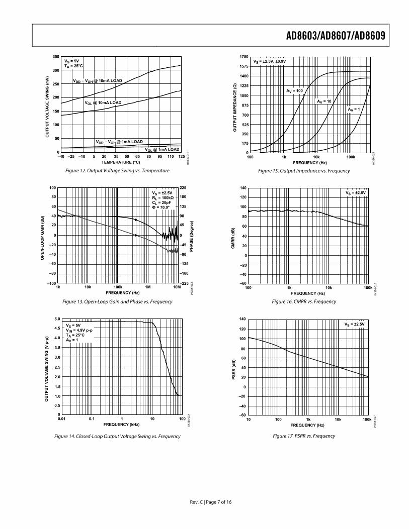
TEMPERATURE (°C)
OU
TPU
T VO
LTA
GE
SWIN
G (m
V)
–400
50
100
350
–25 –10 12520 35 50 65 80 95 1105
150
250
300
200
VOL @ 1mA LOAD
VDD – VOH @ 1mA LOAD
VDD – VOH @ 10mA LOAD
VOL @ 10mA LOAD
VS = 5VTA = 25°C
0435
6-01
2
Figure 12. Output Voltage Swing vs. Temperature
VS = ±2.5VRL = 100kΩCL = 20pFΦ = 70.9°
1k 10k 100k 1M 10MFREQUENCY (Hz)
PHA
SE (D
egre
e)
OPE
N-L
OO
P G
AIN
(dB
)
20
–80
–20
80
100
60
40
0
–40
–60
–100
45
–180
–45
180
225
135
90
0
–90
–135
–225
0435
6-01
3
Figure 13. Open-Loop Gain and Phase vs. Frequency
FREQUENCY (kHz)
OU
TPU
T VO
LTA
GE
SWIN
G (V
p-p
)
0.010
0.5
4.0
5.0
0.1 1 100
4.5
3.5
3.0
2.0
2.5
1.5
1.0
10
VS = 5VVIN = 4.9V p-pTA = 25°CAV = 1
0435
6-01
4
Figure 14. Closed-Loop Output Voltage Swing vs. Frequency
VS = ±2.5V, ±0.9V
AV = 100
AV = 10
AV = 1
FREQUENCY (Hz)
OU
TPU
T IM
PED
AN
CE
(Ω)
100
175
350
1575
01k 100k
1750
1400
1225
875
1050
700
525
10k
0435
6-01
5
Figure 15. Output Impedance vs. Frequency
FREQUENCY (Hz)
CM
RR
(dB
)
100–60
–40
100
140
1k 10k
120
80
60
20
40
0
–20
100k
VS = ±2.5V
0435
6-01
6
Figure 16. CMRR vs. Frequency
10 100 1k 10k 100kFREQUENCY (Hz)
PSR
R (d
B)
0
140
–40
–60
–20
20
60
40
80
120
100
0435
6-01
7
VS = ±2.5V
Figure 17. PSRR vs. Frequency
AD8603/AD8607/AD8609
Rev. C | Page 8 of 16
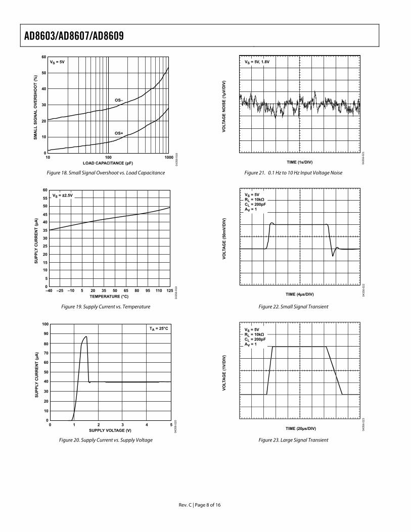
LOAD CAPACITANCE (pF)
SMA
LL S
IGN
AL
OVE
RSH
OO
T (%
)
100
10
20
100 1000
30OS–
50
40
VS = 5V
0435
6-01
8
60
OS+
Figure 18. Small Signal Overshoot vs. Load Capacitance
TEMPERATURE (°C)
SUPP
LY C
UR
REN
T (µ
A)
–40
35
20 80–25 50
60
–10 5 35 65
10
095 110 125
25
50
55
45
40
30
20
15
5
VS = ±2.5V
0435
6-01
9
Figure 19. Supply Current vs. Temperature
SUPPLY VOLTAGE (V)
SUPP
LY C
UR
REN
T (µ
A)
00
30
60
80
2 4 53
20
10
70
50
40
1
100
90
0435
6-02
0
TA = 25°C
Figure 20. Supply Current vs. Supply Voltage
VS = 5V, 1.8V
TIME (1s/DIV)
VOLT
AG
E N
OIS
E (1
µV/D
IV)
0435
6-02
1
Figure 21. 0.1 Hz to 10 Hz Input Voltage Noise
VS = 5VRL = 10kΩCL = 200pFAV = 1
TIME (4µs/DIV)
VOLT
AG
E (5
0mV/
DIV
)
0435
6-02
2
Figure 22. Small Signal Transient
TIME (20µs/DIV)
VOLT
AG
E (1
V/D
IV)
0435
6-02
3
VS = 5VRL = 10kΩCL = 200pFAV = 1
Figure 23. Large Signal Transient
AD8603/AD8607/AD8609
Rev. C | Page 9 of 16
VS = ±2.5VRL = 10kΩAV = 100VIN = 50mV
0V
0V
–50mV
+2.5V
TIME (4μs/DIV))
V IN
(mV)
V OU
T (V
)
TIME (40µs/DIV) 0435
6-02
4
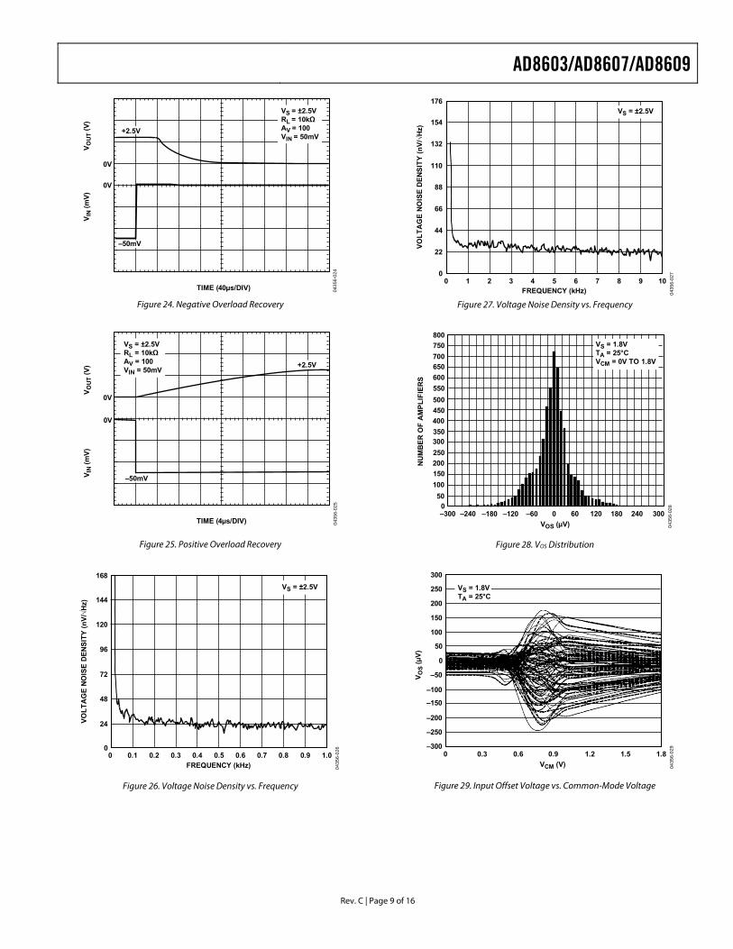
Figure 24. Negative Overload Recovery
VS = ±2.5VRL = 10kΩAV = 100VIN = 50mV
0V
0V
–50mV
+2.5V
TIME (4µs/DIV) 0435
6-02
5
V IN
(mV)
V OU
T (V
)
Figure 25. Positive Overload Recovery
FREQUENCY (kHz)
VOLT
AG
E N
OIS
E D
ENSI
TY (n
V/√H
z)
24
0.1 1.00.2 0.3 0.4 0.5 0.6 0.7 0.8 0.90
48
72
96
120
144
168
0
VS = ±2.5V
0435
6-02
6
Figure 26. Voltage Noise Density vs. Frequency
FREQUENCY (kHz)
VOLT
AG
E N
OIS
E D
ENSI
TY (n
V/√H
z)
22
1 12 3 4 5 6 7 8 90
44
66
88
110
132
176
00
VS = ±2.5V154
0435
6-02
7
Figure 27. Voltage Noise Density vs. Frequency
VOS (µV)
NU
MB
ER O
F A
MPL
IFIE
RS
–3000
300
500
800
–240 60 240–180 –120 120 180 300
400
200
100
700
600
0–60
50
150
250
350
450
550
650
750 VS = 1.8VTA = 25°CVCM = 0V TO 1.8V
0435
6-02
8
Figure 28. VOS Distribution
VCM(V)
V OS
(µV)
0–300
–100
100
300
0.90.60.3 1.5 1.81.2
–200
–150
–250
–50
0
50
150
200
250 VS = 1.8VTA = 25°C
0435
6-02
9
VCM (V)
Figure 29. Input Offset Voltage vs. Common-Mode Voltage
AD8603/AD8607/AD8609
Rev. C | Page 10 of 16
LOAD CURRENT (mA)
OU
TPU
T VO
LTA
GE
TO S
UPP
LY R
AIL
(mV)
0.0010.01
0.1
10
100
0.01 0.1 1 10
1000
1
SINKSOURCE
VS = 1.8VTA = 25°C
0435
6-03
0
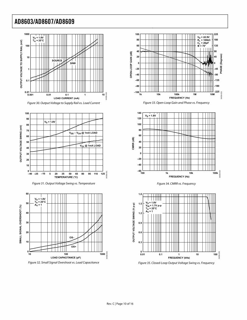
Figure 30. Output Voltage to Supply Rail vs. Load Current
TEMPERATURE (°C)
OU
TPU
T VO
LTA
GE
SWIN
G (m
V)
–400
30
60
5 35 12520
20
10
50
40
–25
70
80
90
100
–10 50 65 80 95 110
VOL @ 1mA LOAD
VDD – VOH @ 1mA LOAD
VS = 1.8V
0435
6-03
1
Figure 31. Output Voltage Swing vs. Temperature
LOAD CAPACITANCE (pF)
SMA
LL S
IGN
AL
OVE
RSH
OO
T (%
)
100
10
20
60
100 1000
30
50
40
VS = 1.8VTA = 25°CAV = 1
OS–
OS+
0435
6-03
2
Figure 32. Small Signal Overshoot vs. Load Capacitance
1k 10k 100k 1M 10M
VS = ±0.9VRL = 100kΩCL = 20pFΦ = 70°
FREQUENCY (Hz)
PHA
SE (D
egre
es)
OPE
N-L
OO
P G
AIN
(dB
)
20
–80
–20
80
100
60
40
0
–40
–60
–100
45
–180
–45
180
225
135
90
0
–90
–135
–225
0435
6-03
3
Figure 33. Open-Loop Gain and Phase vs. Frequency
100 1k 10k 100k
VS = 1.8V
CM
RR
(dB
) 60
–40
20
120
140
100
80
40
0
–20
–60
FREQUENCY (Hz) 0435
6-03
4
Figure 34. CMRR vs. Frequency
0.01 0.1 1 10010FREQUENCY (kHz)
OU
TPU
T VO
LTA
GE
SWIN
G (V
p-p
)
0
0.9
1.8
0.6
0.3
1.5
1.2
VS = 1.8VVIN = 1.7V p-pTA = 25°CAV = 1
0435
6-03
5
Figure 35. Closed-Loop Output Voltage Swing vs. Frequency
AD8603/AD8607/AD8609
Rev. C | Page 11 of 16
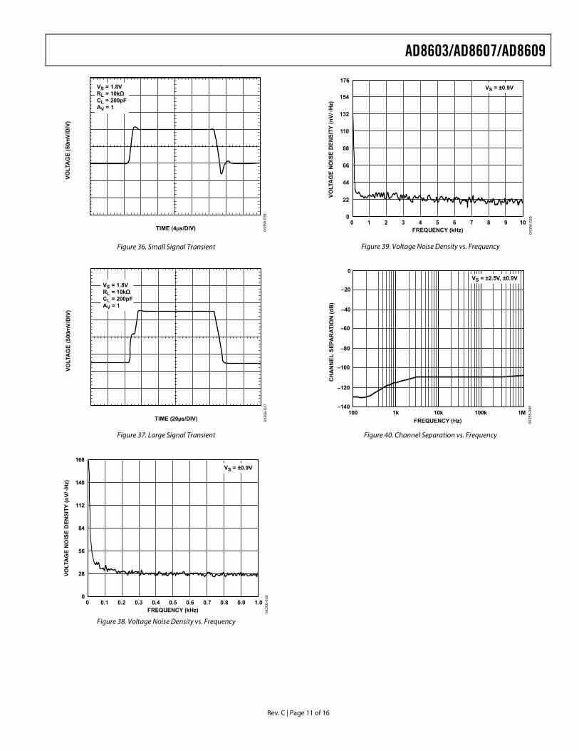
VS = 1.8VRL = 10kΩCL = 200pFAV = 1
VOLT
AG
E (5
0mV/
DIV
)
TIME (4µs/DIV) 0435
6-03
6
Figure 36. Small Signal Transient
VS = 1.8VRL = 10kΩCL = 200pFAV = 1
VOLT
AG
E (5
00m
V/D
IV)
TIME (20µs/DIV) 0435
6-03
7
Figure 37. Large Signal Transient
FREQUENCY (kHz)
VOLT
AG
E N
OIS
E D
ENSI
TY (n
V/√H
z)
28
0.1 1.00.2 0.3 0.4 0.5 0.6 0.7 0.8 0.90
56
84
112
140
168
0
VS = ±0.9V
0435
6-03
8
Figure 38. Voltage Noise Density vs. Frequency
FREQUENCY (kHz)
VOLT
AG
E N
OIS
E D
ENSI
TY (n
V/√H
z)
22
1 12 3 4 5 6 7 8 90
44
66
88
110
132
176
00
VS = ±0.9V154
0435
6-03
9
Figure 39. Voltage Noise Density vs. Frequency
FREQUENCY (Hz)
CH
AN
NE
L SE
PAR
ATIO
N (d
B)
100
–120
–40
–20
0
1k 10k 100k 1M
–60
–140
–80
–100
VS = ±2.5V, ±0.9V
0435
6-04
0
Figure 40. Channel Separation vs. Frequency
AD8603/AD8607/AD8609
Rev. C | Page 12 of 16
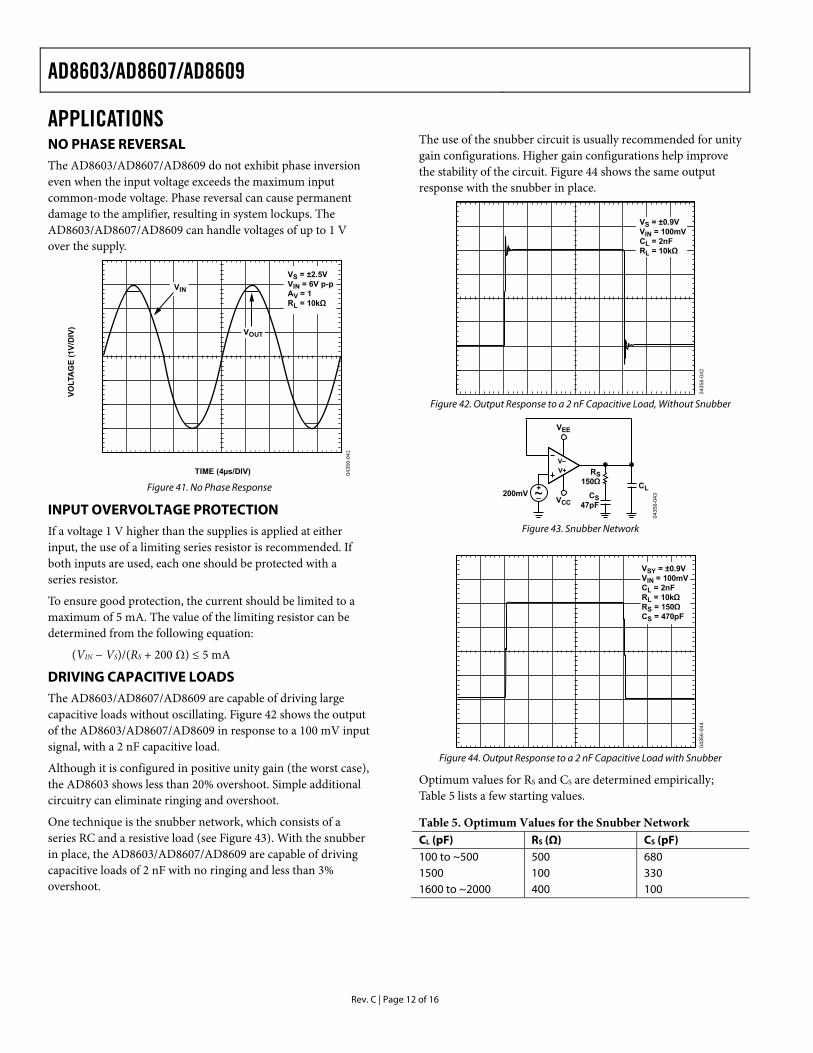
APPLICATIONS NO PHASE REVERSAL The AD8603/AD8607/AD8609 do not exhibit phase inversion even when the input voltage exceeds the maximum input common-mode voltage. Phase reversal can cause permanent damage to the amplifier, resulting in system lockups. The AD8603/AD8607/AD8609 can handle voltages of up to 1 V over the supply.
VOLT
AG
E (1
V/D
IV)
TIME (4µs/DIV)
VS = ±2.5VVIN = 6V p-pAV = 1RL = 10kΩ
VIN
VOUT
0435
6-04
1
Figure 41. No Phase Response
INPUT OVERVOLTAGE PROTECTION If a voltage 1 V higher than the supplies is applied at either input, the use of a limiting series resistor is recommended. If both inputs are used, each one should be protected with a series resistor.
To ensure good protection, the current should be limited to a maximum of 5 mA. The value of the limiting resistor can be determined from the following equation:
(VIN − VS)/(RS + 200 Ω) ≤ 5 mA
DRIVING CAPACITIVE LOADS The AD8603/AD8607/AD8609 are capable of driving large capacitive loads without oscillating. Figure 42 shows the output of the AD8603/AD8607/AD8609 in response to a 100 mV input signal, with a 2 nF capacitive load.
Although it is configured in positive unity gain (the worst case), the AD8603 shows less than 20% overshoot. Simple additional circuitry can eliminate ringing and overshoot.
One technique is the snubber network, which consists of a series RC and a resistive load (see Figure 43). With the snubber in place, the AD8603/AD8607/AD8609 are capable of driving capacitive loads of 2 nF with no ringing and less than 3% overshoot.
The use of the snubber circuit is usually recommended for unity gain configurations. Higher gain configurations help improve the stability of the circuit. Figure 44 shows the same output response with the snubber in place.
VS = ±0.9VVIN = 100mVCL = 2nFRL = 10kΩ
0435
6-04
2
Figure 42. Output Response to a 2 nF Capacitive Load, Without Snubber
0435
6-04
3CS47pFVCC
VEE
RS150Ω
200mVCL
V+V–
–+
Figure 43. Snubber Network
VSY = ±0.9VVIN = 100mVCL = 2nFRL = 10kΩRS = 150ΩCS = 470pF
0435
6-04
4
Figure 44. Output Response to a 2 nF Capacitive Load with Snubber
Optimum values for RS and CS are determined empirically; Table 5 lists a few starting values.
Table 5. Optimum Values for the Snubber Network CL (pF) RS (Ω) CS (pF) 100 to ~500 500 680 1500 100 330 1600 to ~2000 400 100
AD8603/AD8607/AD8609
Rev. C | Page 13 of 16
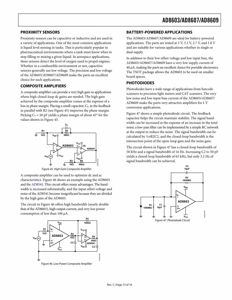
PROXIMITY SENSORS Proximity sensors can be capacitive or inductive and are used in a variety of applications. One of the most common applications is liquid level sensing in tanks. This is particularly popular in pharmaceutical environments where a tank must know when to stop filling or mixing a given liquid. In aerospace applications, these sensors detect the level of oxygen used to propel engines. Whether in a combustible environment or not, capacitive sensors generally use low voltage. The precision and low voltage of the AD8603/AD8607/AD8609 make the parts an excellent choice for such applications.
COMPOSITE AMPLIFIERS A composite amplifier can provide a very high gain in applications where high closed-loop dc gains are needed. The high gain achieved by the composite amplifier comes at the expense of a loss in phase margin. Placing a small capacitor, CF, in the feedback in parallel with R2 (see Figure 45) improves the phase margin. Picking CF = 50 pF yields a phase margin of about 45° for the values shown in Figure 45.
VEE
VCC
R1
CF
1kΩ
VCC
VEE
VIN
99kΩ
R2
AD8603AD8541V+
V–V+
V–
R3 R499kΩ1kΩ
U5
0435
6-04
5
Figure 45. High Gain Composite Amplifier
A composite amplifier can be used to optimize dc and ac characteristics. Figure 46 shows an example using the AD8603 and the AD8541. This circuit offers many advantages. The band-width is increased substantially, and the input offset voltage and noise of the AD8541 become insignificant because they are divided by the high gain of the AD8603.
The circuit in Figure 46 offers high bandwidth (nearly double that of the AD8603), high output current, and very low power consumption of less than 100 μA.
R1
1kΩ V+V–
VIN
100kΩ
R2
AD8541100Ω
C3
1kΩR4
R3
C2
VCC
VEE
0435
6-04
6
VCC
VEE
V–
V+
AD8603
Figure 46. Low Power Composite Amplifier
BATTERY-POWERED APPLICATIONS The AD8603/AD8607/AD8609 are ideal for battery-powered applications. The parts are tested at 5 V, 3.3 V, 2.7 V, and 1.8 V and are suitable for various applications whether in single or dual supply.
In addition to their low offset voltage and low input bias, the AD8603/AD8607/AD8609 have a very low supply current of 40 μA, making the parts an excellent choice for portable electronics. The TSOT package allows the AD8603 to be used on smaller board spaces.
PHOTODIODES Photodiodes have a wide range of applications from barcode scanners to precision light meters and CAT scanners. The very low noise and low input bias current of the AD8603/AD8607/ AD8609 make the parts very attractive amplifiers for I-V conversion applications.
Figure 47 shows a simple photodiode circuit. The feedback capacitor helps the circuit maintain stability. The signal band-width can be increased at the expense of an increase in the total noise; a low-pass filter can be implemented by a simple RC network at the output to reduce the noise. The signal bandwidth can be calculated by ½πR2C2, and the closed-loop bandwidth is the intersection point of the open-loop gain and the noise gain.
The circuit shown in Figure 47 has a closed-loop bandwidth of 58 kHz and a signal bandwidth of 16 Hz. Increasing C2 to 50 pF yields a closed-loop bandwidth of 65 kHz, but only 3.2 Hz of signal bandwidth can be achieved.
C210pF
R21000MΩ
R11000MΩ
VCC
VEE
V–
V+
AD8603C1
10pF04
356-
047
Figure 47. Photodiode Circuit
AD8603/AD8607/AD8609
Rev. C | Page 14 of 16
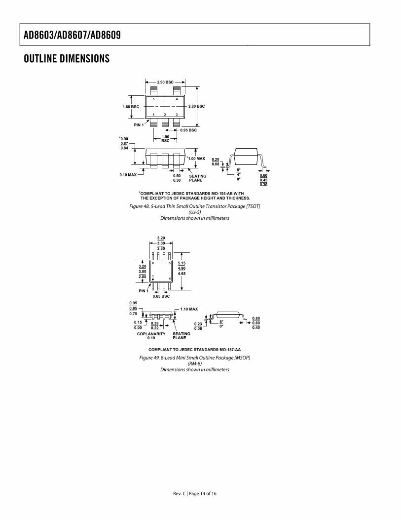
OUTLINE DIMENSIONS
*COMPLIANT TO JEDEC STANDARDS MO-193-AB WITHTHE EXCEPTION OF PACKAGE HEIGHT AND THICKNESS.
PIN 1
1.60 BSC 2.80 BSC
1.90BSC
0.95 BSC
0.200.08
0.600.450.30
8°4°0°
0.500.30
0.10 MAX SEATINGPLANE
*1.00 MAX
*0.900.870.84
2.90 BSC
5 4
1 2 3
Figure 48. 5-Lead Thin Small Outline Transistor Package [TSOT]
(UJ-5) Dimensions shown in millimeters
COMPLIANT TO JEDEC STANDARDS MO-187-AA
0.800.600.40
8°0°
4
8
1
5
PIN 10.65 BSC
SEATINGPLANE
0.380.22
1.10 MAX
3.203.002.80
COPLANARITY0.10
0.230.08
3.203.002.80
5.154.904.65
0.150.00
0.950.850.75
Figure 49. 8-Lead Mini Small Outline Package [MSOP]
(RM-8) Dimensions shown in millimeters
AD8603/AD8607/AD8609
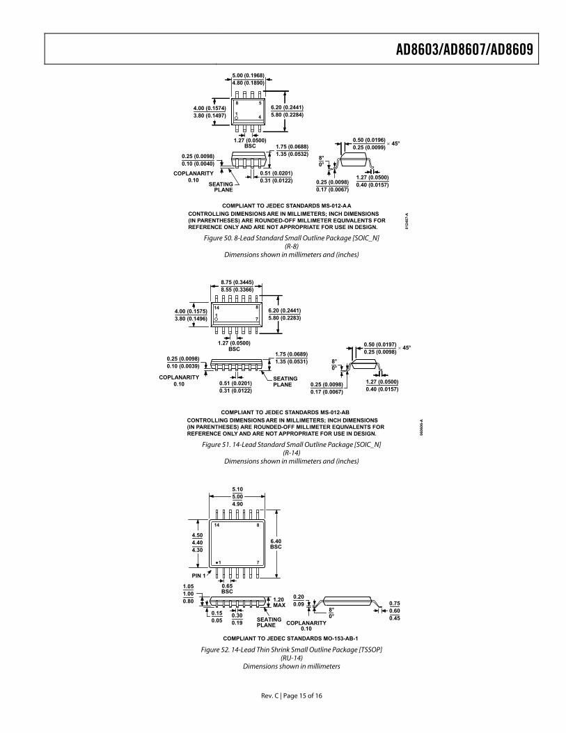
Rev. C | Page 15 of 16
CONTROLLING DIMENSIONS ARE IN MILLIMETERS; INCH DIMENSIONS(IN PARENTHESES) ARE ROUNDED-OFF MILLIMETER EQUIVALENTS FORREFERENCE ONLY AND ARE NOT APPROPRIATE FOR USE IN DESIGN.
COMPLIANT TO JEDEC STANDARDS MS-012-AA
0124
07-A
0.25 (0.0098)0.17 (0.0067)
1.27 (0.0500)0.40 (0.0157)
0.50 (0.0196)0.25 (0.0099)
45°
8°0°
1.75 (0.0688)1.35 (0.0532)
SEATINGPLANE
0.25 (0.0098)0.10 (0.0040)
41
8 5
5.00 (0.1968)4.80 (0.1890)
4.00 (0.1574)3.80 (0.1497)
1.27 (0.0500)BSC
6.20 (0.2441)5.80 (0.2284)
0.51 (0.0201)0.31 (0.0122)
COPLANARITY0.10
Figure 50. 8-Lead Standard Small Outline Package [SOIC_N]
(R-8) Dimensions shown in millimeters and (inches)
CONTROLLING DIMENSIONS ARE IN MILLIMETERS; INCH DIMENSIONS(IN PARENTHESES) ARE ROUNDED-OFF MILLIMETER EQUIVALENTS FORREFERENCE ONLY AND ARE NOT APPROPRIATE FOR USE IN DESIGN.
COMPLIANT TO JEDEC STANDARDS MS-012-AB06
0606
-A
14 8
71
6.20 (0.2441)5.80 (0.2283)
4.00 (0.1575)3.80 (0.1496)
8.75 (0.3445)8.55 (0.3366)
1.27 (0.0500)BSC
SEATINGPLANE
0.25 (0.0098)0.10 (0.0039)
0.51 (0.0201)0.31 (0.0122)
1.75 (0.0689)1.35 (0.0531)
0.50 (0.0197)0.25 (0.0098)
1.27 (0.0500)0.40 (0.0157)
0.25 (0.0098)0.17 (0.0067)
COPLANARITY0.10
8°0°
45°
Figure 51. 14-Lead Standard Small Outline Package [SOIC_N]
(R-14) Dimensions shown in millimeters and (inches)
4.504.404.30
14 8
71
6.40BSC
PIN 1
5.105.004.90
0.65BSC
SEATINGPLANE
0.150.05
0.300.19
1.20MAX
1.051.000.80
0.200.09
8°0°
0.750.600.45
COPLANARITY0.10
COMPLIANT TO JEDEC STANDARDS MO-153-AB-1 Figure 52. 14-Lead Thin Shrink Small Outline Package [TSSOP]
(RU-14) Dimensions shown in millimeters
AD8603/AD8607/AD8609
Rev. C | Page 16 of 16
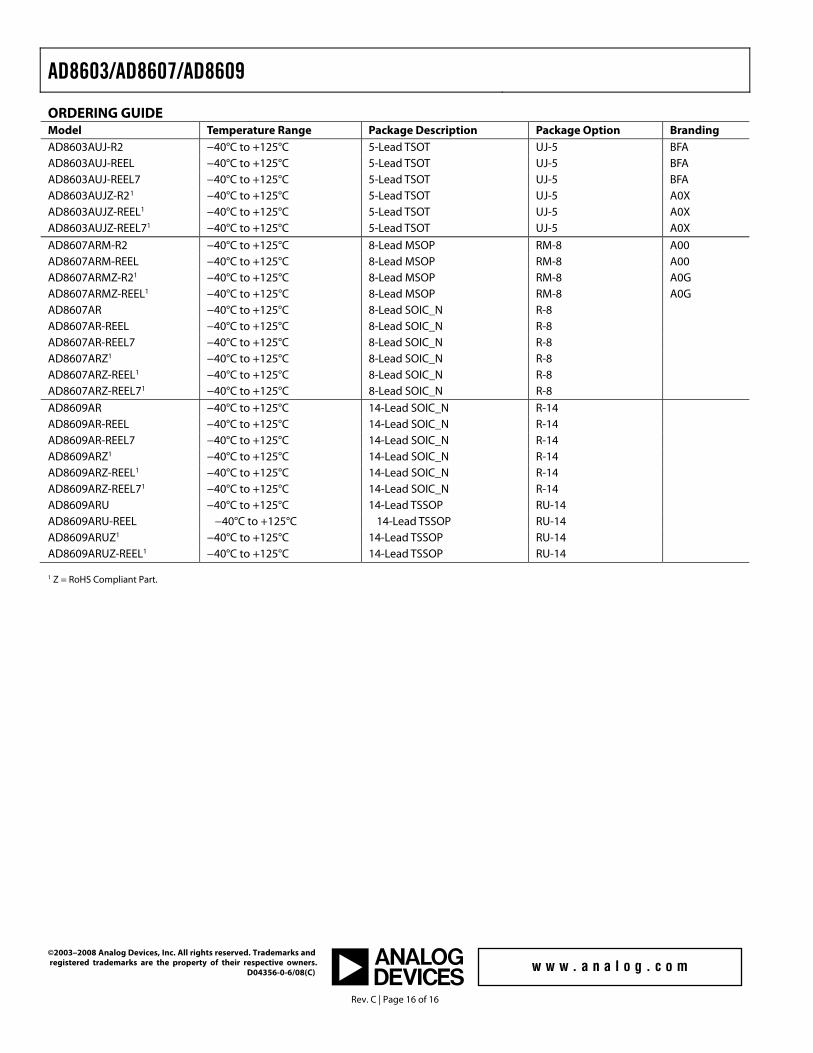
ORDERING GUIDE Model Temperature Range Package Description Package Option Branding AD8603AUJ-R2 −40°C to +125°C 5-Lead TSOT UJ-5 BFA AD8603AUJ-REEL −40°C to +125°C 5-Lead TSOT UJ-5 BFA AD8603AUJ-REEL7 −40°C to +125°C 5-Lead TSOT UJ-5 BFA AD8603AUJZ-R21
−40°C to +125°C 5-Lead TSOT UJ-5 A0X AD8603AUJZ-REEL1
−40°C to +125°C 5-Lead TSOT UJ-5 A0X AD8603AUJZ-REEL71
−40°C to +125°C 5-Lead TSOT UJ-5 A0X
AD8607ARM-R2 −40°C to +125°C 8-Lead MSOP RM-8 A00 AD8607ARM-REEL −40°C to +125°C 8-Lead MSOP RM-8 A00 AD8607ARMZ-R21
−40°C to +125°C 8-Lead MSOP RM-8 A0G AD8607ARMZ-REEL1
−40°C to +125°C 8-Lead MSOP RM-8 A0G AD8607AR −40°C to +125°C 8-Lead SOIC_N R-8 AD8607AR-REEL −40°C to +125°C 8-Lead SOIC_N R-8 AD8607AR-REEL7 −40°C to +125°C 8-Lead SOIC_N R-8 AD8607ARZ1
−40°C to +125°C 8-Lead SOIC_N R-8 AD8607ARZ-REEL1
−40°C to +125°C 8-Lead SOIC_N R-8 AD8607ARZ-REEL71
−40°C to +125°C 8-Lead SOIC_N R-8 AD8609AR −40°C to +125°C 14-Lead SOIC_N R-14 AD8609AR-REEL −40°C to +125°C 14-Lead SOIC_N R-14 AD8609AR-REEL7 −40°C to +125°C 14-Lead SOIC_N R-14 AD8609ARZ1
−40°C to +125°C 14-Lead SOIC_N R-14 AD8609ARZ-REEL1
−40°C to +125°C 14-Lead SOIC_N R-14 AD8609ARZ-REEL71
−40°C to +125°C 14-Lead SOIC_N R-14 AD8609ARU −40°C to +125°C 14-Lead TSSOP RU-14 AD8609ARU-REEL −40°C to +125°C 14-Lead TSSOP RU-14 AD8609ARUZ1
−40°C to +125°C 14-Lead TSSOP RU-14 AD8609ARUZ-REEL1
−40°C to +125°C 14-Lead TSSOP RU-14 1 Z = RoHS Compliant Part.
©2003–2008 Analog Devices, Inc. All rights reserved. Trademarks and registered trademarks are the property of their respective owners. D04356-0-6/08(C)