Embed Size (px)
Citation preview
REV. 0
Information furnished by Analog Devices is believed to be accurate andreliable. However, no responsibility is assumed by Analog Devices for itsuse, nor for any infringements of patents or other rights of third partieswhich may result from its use. No license is granted by implication orotherwise under any patent or patent rights of Analog Devices.
aAD9841A/AD9842A
One Technology Way, P.O. Box 9106, Norwood, MA 02062-9106, U.S.A.
Tel: 781/329-4700 World Wide Web Site: http://www.analog.com
Fax: 781/326-8703 © Analog Devices, Inc., 2001
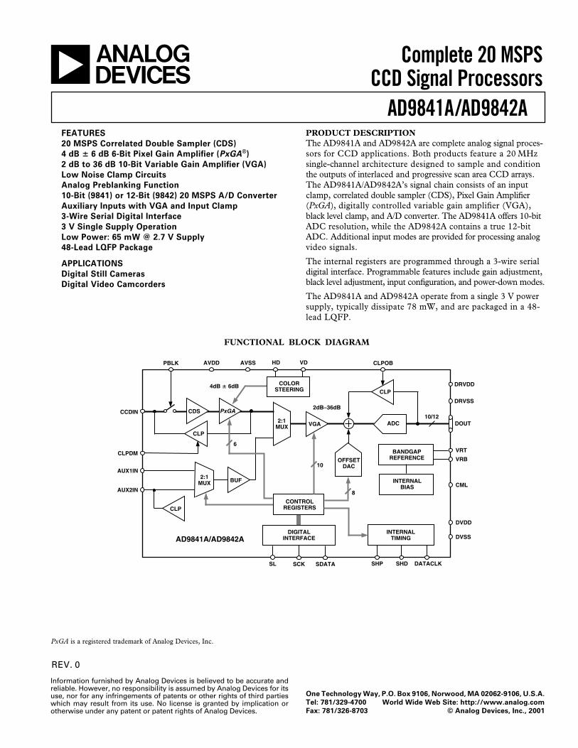
Complete 20 MSPSCCD Signal Processors
FUNCTIONAL BLOCK DIAGRAM
DATACLKSHDSHP
BANDGAPREFERENCE
2:1MUX DOUT
AUX2IN
CLPDM
CCDIN
OFFSETDAC
PBLK
AUX1IN
VRT
VRB
INTERNALTIMING
INTERNALBIAS
2dB–36dB
AVDD
DVDD
DVSS
AVSS
DRVDD
DRVSS
10
8CML
DIGITALINTERFACE
SDATASCKSL
CLPOB
10/12CDS
VGA
CLP
BUF2:1MUX
CLP
AD9841A/AD9842A
CONTROLREGISTERS
CLP
ADC
4dB � 6dB COLORSTEERING
HD VD
PxGA
6
FEATURES
20 MSPS Correlated Double Sampler (CDS)
4 dB � 6 dB 6-Bit Pixel Gain Amplifier (PxGA®)
2 dB to 36 dB 10-Bit Variable Gain Amplifier (VGA)
Low Noise Clamp Circuits
Analog Preblanking Function
10-Bit (9841) or 12-Bit (9842) 20 MSPS A/D Converter
Auxiliary Inputs with VGA and Input Clamp
3-Wire Serial Digital Interface
3 V Single Supply Operation
Low Power: 65 mW @ 2.7 V Supply
48-Lead LQFP Package
APPLICATIONS
Digital Still Cameras
Digital Video Camcorders
PRODUCT DESCRIPTIONThe AD9841A and AD9842A are complete analog signal proces-sors for CCD applications. Both products feature a 20 MHzsingle-channel architecture designed to sample and conditionthe outputs of interlaced and progressive scan area CCD arrays.The AD9841A/AD9842A’s signal chain consists of an inputclamp, correlated double sampler (CDS), Pixel Gain Amplifier(PxGA), digitally controlled variable gain amplifier (VGA),black level clamp, and A/D converter. The AD9841A offers 10-bitADC resolution, while the AD9842A contains a true 12-bitADC. Additional input modes are provided for processing analogvideo signals.
The internal registers are programmed through a 3-wire serialdigital interface. Programmable features include gain adjustment,black level adjustment, input configuration, and power-down modes.
The AD9841A and AD9842A operate from a single 3 V powersupply, typically dissipate 78 mW, and are packaged in a 48-lead LQFP.
PxGA is a registered trademark of Analog Devices, Inc.
REV. 0–2–
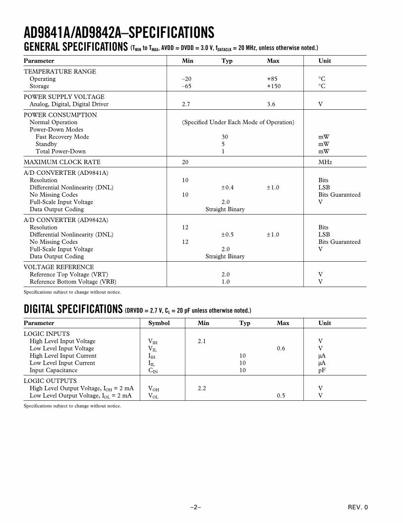
AD9841A/AD9842A–SPECIFICATIONSGENERAL SPECIFICATIONSParameter Min Typ Max Unit
TEMPERATURE RANGEOperating –20 +85 °CStorage –65 +150 °C
POWER SUPPLY VOLTAGEAnalog, Digital, Digital Driver 2.7 3.6 V
POWER CONSUMPTIONNormal Operation (Specified Under Each Mode of Operation)Power-Down Modes
Fast Recovery Mode 30 mWStandby 5 mWTotal Power-Down 1 mW
MAXIMUM CLOCK RATE 20 MHz
A/D CONVERTER (AD9841A)Resolution 10 BitsDifferential Nonlinearity (DNL) ±0.4 ±1.0 LSBNo Missing Codes 10 Bits GuaranteedFull-Scale Input Voltage 2.0 VData Output Coding Straight Binary
A/D CONVERTER (AD9842A)Resolution 12 BitsDifferential Nonlinearity (DNL) ±0.5 ±1.0 LSBNo Missing Codes 12 Bits GuaranteedFull-Scale Input Voltage 2.0 VData Output Coding Straight Binary
VOLTAGE REFERENCEReference Top Voltage (VRT) 2.0 VReference Bottom Voltage (VRB) 1.0 V
Specifications subject to change without notice.
DIGITAL SPECIFICATIONSParameter Symbol Min Typ Max Unit
LOGIC INPUTSHigh Level Input Voltage VIH 2.1 VLow Level Input Voltage VIL 0.6 VHigh Level Input Current IIH 10 µALow Level Input Current IIL 10 µAInput Capacitance CIN 10 pF
LOGIC OUTPUTSHigh Level Output Voltage, IOH = 2 mA VOH 2.2 VLow Level Output Voltage, IOL = 2 mA VOL 0.5 V
Specifications subject to change without notice.
(DRVDD = 2.7 V, CL = 20 pF unless otherwise noted.)
(TMIN to TMAX, AVDD = DVDD = 3.0 V, fDATACLK = 20 MHz, unless otherwise noted.)
REV. 0 –3–
AD9841A/AD9842A
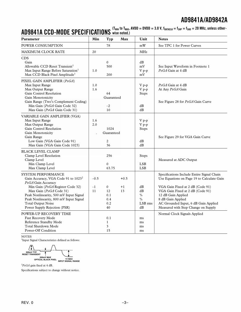
Parameter Min Typ Max Unit Notes
POWER CONSUMPTION 78 mW See TPC 1 for Power Curves
MAXIMUM CLOCK RATE 20 MHz
CDSGain 0 dBAllowable CCD Reset Transient1 500 mV See Input Waveform in Footnote 1Max Input Range Before Saturation1 1.0 V p-p PxGA Gain at 4 dBMax CCD Black Pixel Amplitude1 200 mV
PIXEL GAIN AMPLIFIER (PxGA)Max Input Range 1.0 V p-p PxGA Gain at 4 dBMax Output Range 1.6 V p-p At Any PxGA GainGain Control Resolution 64 StepsGain Monotonicity GuaranteedGain Range (Two’s Complement Coding) See Figure 28 for PxGA Gain Curve
Min Gain (PxGA Gain Code 32) –2 dBMax Gain (PxGA Gain Code 31) 10 dB
VARIABLE GAIN AMPLIFIER (VGA)Max Input Range 1.6 V p-pMax Output Range 2.0 V p-pGain Control Resolution 1024 StepsGain Monotonicity . GuaranteedGain Range See Figure 29 for VGA Gain Curve
Low Gain (VGA Gain Code 91) 2 dBMax Gain (VGA Gain Code 1023) 36 dB
BLACK LEVEL CLAMPClamp Level Resolution 256 StepsClamp Level Measured at ADC Output
Min Clamp Level 0 LSBMax Clamp Level 63.75 LSB
SYSTEM PERFORMANCE Specifications Include Entire Signal ChainGain Accuracy, VGA Code 91 to 10232 –0.5 +0.5 Use Equations on Page 19 to Calculate GainPxGA Gain Accuracy
Min Gain (PxGA Register Code 32) –1 0 +1 dB VGA Gain Fixed at 2 dB (Code 91)Max Gain (PxGA Code 31) 11 12 13 dB VGA Gain Fixed at 2 dB (Code 91)
Peak Nonlinearity, 500 mV Input Signal 0.1 % 12 dB Gain AppliedPeak Nonlinearity, 800 mV Input Signal 0.4 % 8 dB Gain AppliedTotal Output Noise 0.2 LSB rms AC Grounded Input, 6 dB Gain AppliedPower Supply Rejection (PSR) 40 dB Measured with Step Change on Supply
POWER-UP RECOVERY TIME Normal Clock Signals AppliedFast Recovery Mode 0.1 msReference Standby Mode 1 msTotal Shutdown Mode 3 msPower-Off Condition 15 ms
NOTES1Input Signal Characteristics defined as follows:
200mV MAXOPTICAL BLACK PIXEL
500mV TYPRESET TRANSIENT
1V MAXINPUT SIGNAL RANGE
2PxGA gain fixed at 4 dB.
Specifications subject to change without notice.
AD9841A CCD-MODE SPECIFICATIONS(TMIN to TMAX, AVDD = DVDD = 3.0 V, fDATACLK = fSHP = fSHD = 20 MHz, unless other-wise noted.)
REV. 0–4–
AD9841A/AD9842A–SPECIFICATIONS
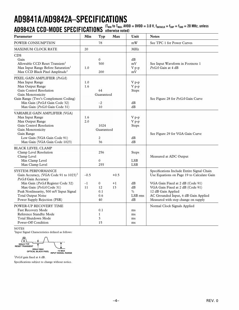
Parameter Min Typ Max Unit Notes
POWER CONSUMPTION 78 mW See TPC 1 for Power Curves
MAXIMUM CLOCK RATE 20 MHz
CDSGain 0 dBAllowable CCD Reset Transient1 500 mV See Input Waveform in Footnote 1Max Input Range Before Saturation1 1.0 V p-p PxGA Gain at 4 dBMax CCD Black Pixel Amplitude1 200 mV
PIXEL GAIN AMPLIFIER (PxGA)Max Input Range 1.0 V p-pMax Output Range 1.6 V p-pGain Control Resolution 64 StepsGain Monotonicity Guaranteed
Gain Range (Two’s Complement Coding) See Figure 28 for PxGA Gain CurveMin Gain (PxGA Gain Code 32) –2 dBMax Gain (PxGA Gain Code 31) 10 dB
VARIABLE GAIN AMPLIFIER (VGA)Max Input Range 1.6 V p-pMax Output Range 2.0 V p-pGain Control Resolution 1024 StepsGain Monotonicity GuaranteedGain Range See Figure 29 for VGA Gain Curve
Low Gain (VGA Gain Code 91) 2 dBMax Gain (VGA Gain Code 1023) 36 dB
BLACK LEVEL CLAMPClamp Level Resolution 256 StepsClamp Level Measured at ADC Output
Min Clamp Level 0 LSBMax Clamp Level 255 LSB
SYSTEM PERFORMANCE Specifications Include Entire Signal ChainGain Accuracy, (VGA Code 91 to 1023)2 –0.5 +0.5 Use Equations on Page 19 to Calculate GainPxGA Gain Accuracy
Min Gain (PxGA Register Code 32) –1 0 +1 dB VGA Gain Fixed at 2 dB (Code 91)Max Gain (PxGA Code 31) 11 12 13 dB VGA Gain Fixed at 2 dB (Code 91)
Peak Nonlinearity, 500 mV Input Signal 0.1 % 12 dB Gain AppliedTotal Output Noise 0.6 LSB rms AC Grounded Input, 6 dB Gain AppliedPower Supply Rejection (PSR) 40 dB Measured with step change on supply
POWER-UP RECOVERY TIME Normal Clock Signals AppliedFast Recovery Mode 0.1 msReference Standby Mode 1 msTotal Shutdown Mode 3 msPower-Off Condition 15 ms
NOTES1Input Signal Characteristics defined as follows:
200mV MAXOPTICAL BLACK PIXEL
500mV TYPRESET TRANSIENT
1V MAXINPUT SIGNAL RANGE
2PxGA gain fixed at 4 dB.
Specifications subject to change without notice.
AD9842A CCD-MODE SPECIFICATIONS(TMIN to TMAX, AVDD = DVDD = 3.0 V, fDATACLK = fSHP = fSHD = 20 MHz, unlessotherwise noted)
REV. 0 –5–
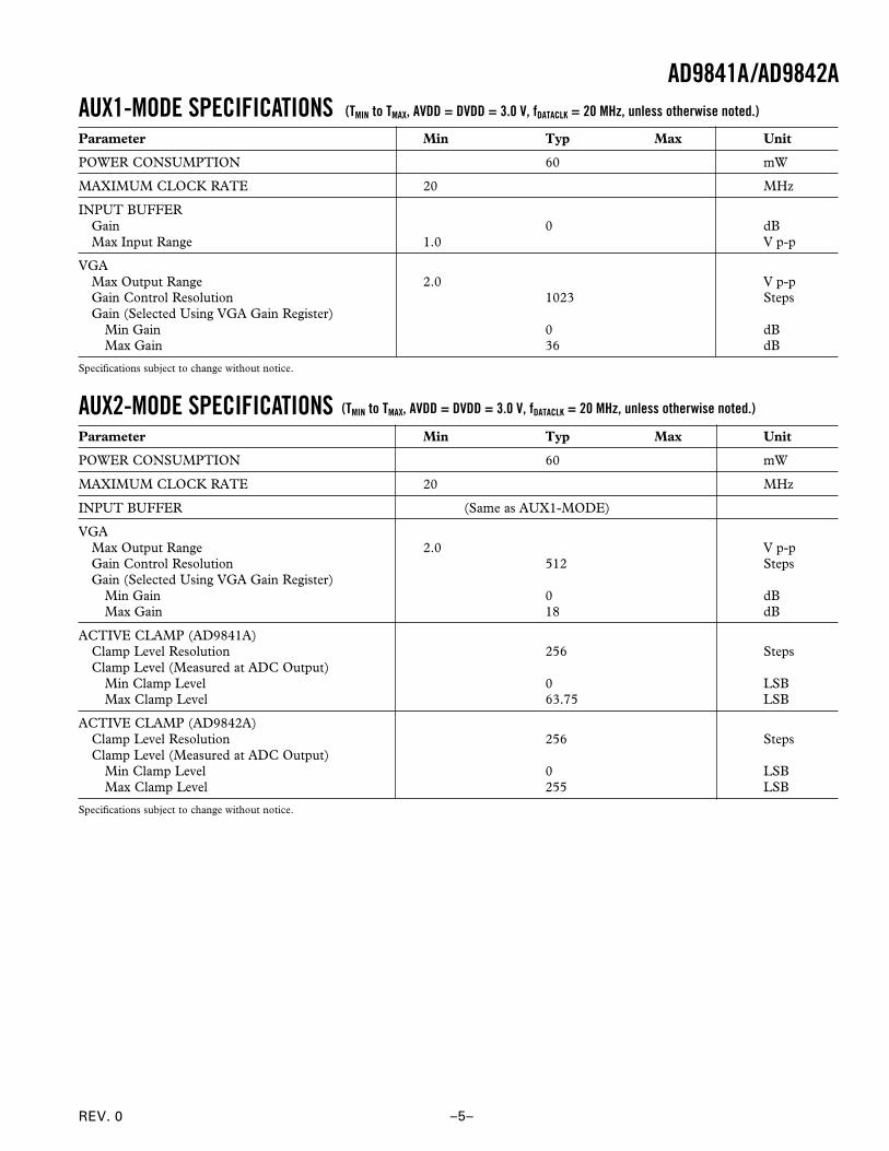
AD9841A/AD9842AAUX1-MODE SPECIFICATIONSParameter Min Typ Max Unit
POWER CONSUMPTION 60 mW
MAXIMUM CLOCK RATE 20 MHz
INPUT BUFFERGain 0 dBMax Input Range 1.0 V p-p
VGAMax Output Range 2.0 V p-pGain Control Resolution 1023 StepsGain (Selected Using VGA Gain Register)
Min Gain 0 dBMax Gain 36 dB
Specifications subject to change without notice.
AUX2-MODE SPECIFICATIONSParameter Min Typ Max Unit
POWER CONSUMPTION 60 mW
MAXIMUM CLOCK RATE 20 MHz
INPUT BUFFER (Same as AUX1-MODE)
VGAMax Output Range 2.0 V p-pGain Control Resolution 512 StepsGain (Selected Using VGA Gain Register)
Min Gain 0 dBMax Gain 18 dB
ACTIVE CLAMP (AD9841A)Clamp Level Resolution 256 StepsClamp Level (Measured at ADC Output)
Min Clamp Level 0 LSBMax Clamp Level 63.75 LSB
ACTIVE CLAMP (AD9842A)Clamp Level Resolution 256 StepsClamp Level (Measured at ADC Output)
Min Clamp Level 0 LSBMax Clamp Level 255 LSB
Specifications subject to change without notice.
(TMIN to TMAX, AVDD = DVDD = 3.0 V, fDATACLK = 20 MHz, unless otherwise noted.)
(TMIN to TMAX, AVDD = DVDD = 3.0 V, fDATACLK = 20 MHz, unless otherwise noted.)
REV. 0
AD9841A/AD9842A
–6–
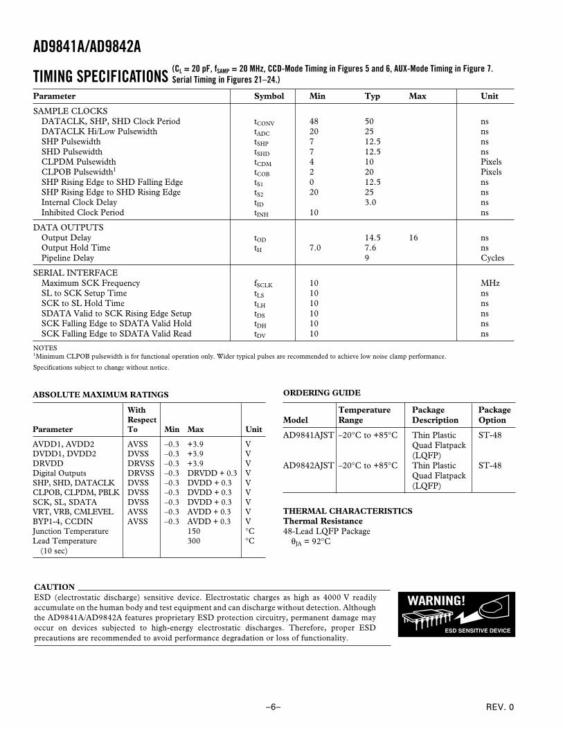
TIMING SPECIFICATIONSParameter Symbol Min Typ Max Unit
SAMPLE CLOCKSDATACLK, SHP, SHD Clock Period tCONV 48 50 nsDATACLK Hi/Low Pulsewidth tADC 20 25 nsSHP Pulsewidth tSHP 7 12.5 nsSHD Pulsewidth tSHD 7 12.5 nsCLPDM Pulsewidth tCDM 4 10 PixelsCLPOB Pulsewidth1 tCOB 2 20 PixelsSHP Rising Edge to SHD Falling Edge tS1 0 12.5 nsSHP Rising Edge to SHD Rising Edge tS2 20 25 nsInternal Clock Delay tID 3.0 nsInhibited Clock Period tINH 10 ns
DATA OUTPUTSOutput Delay tOD 14.5 16 nsOutput Hold Time tH 7.0 7.6 nsPipeline Delay 9 Cycles
SERIAL INTERFACEMaximum SCK Frequency fSCLK 10 MHzSL to SCK Setup Time tLS 10 nsSCK to SL Hold Time tLH 10 nsSDATA Valid to SCK Rising Edge Setup tDS 10 nsSCK Falling Edge to SDATA Valid Hold tDH 10 nsSCK Falling Edge to SDATA Valid Read tDV 10 ns
NOTES1Minimum CLPOB pulsewidth is for functional operation only. Wider typical pulses are recommended to achieve low noise clamp performance.
Specifications subject to change without notice.
CAUTIONESD (electrostatic discharge) sensitive device. Electrostatic charges as high as 4000 V readilyaccumulate on the human body and test equipment and can discharge without detection. Althoughthe AD9841A/AD9842A features proprietary ESD protection circuitry, permanent damage mayoccur on devices subjected to high-energy electrostatic discharges. Therefore, proper ESDprecautions are recommended to avoid performance degradation or loss of functionality.
WARNING!
ESD SENSITIVE DEVICE
(CL = 20 pF, fSAMP = 20 MHz, CCD-Mode Timing in Figures 5 and 6, AUX-Mode Timing in Figure 7.Serial Timing in Figures 21–24.)
ABSOLUTE MAXIMUM RATINGS
WithRespect
Parameter To Min Max Unit
AVDD1, AVDD2 AVSS –0.3 +3.9 VDVDD1, DVDD2 DVSS –0.3 +3.9 VDRVDD DRVSS –0.3 +3.9 VDigital Outputs DRVSS –0.3 DRVDD + 0.3 VSHP, SHD, DATACLK DVSS –0.3 DVDD + 0.3 VCLPOB, CLPDM, PBLK DVSS –0.3 DVDD + 0.3 VSCK, SL, SDATA DVSS –0.3 DVDD + 0.3 VVRT, VRB, CMLEVEL AVSS –0.3 AVDD + 0.3 VBYP1-4, CCDIN AVSS –0.3 AVDD + 0.3 VJunction Temperature 150 °CLead Temperature 300 °C
(10 sec)
ORDERING GUIDE
Temperature Package PackageModel Range Description Option
AD9841AJST –20°C to +85°C Thin Plastic ST-48Quad Flatpack(LQFP)
AD9842AJST –20°C to +85°C Thin Plastic ST-48Quad Flatpack(LQFP)
THERMAL CHARACTERISTICSThermal Resistance48-Lead LQFP Package
θJA = 92°C
REV. 0
AD9841A/AD9842A
–7–
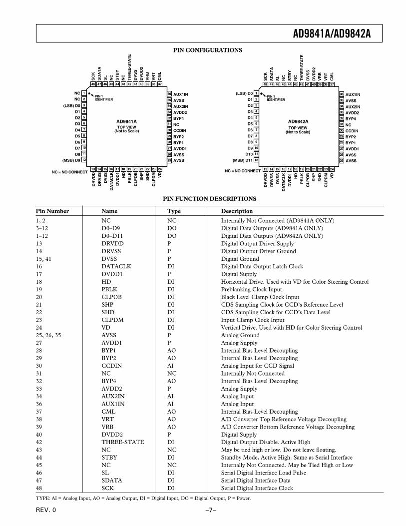
PIN FUNCTION DESCRIPTIONS
Pin Number Name Type Description
1, 2 NC NC Internally Not Connected (AD9841A ONLY)3–12 D0–D9 DO Digital Data Outputs (AD9841A ONLY)1–12 D0–D11 DO Digital Data Outputs (AD9842A ONLY)13 DRVDD P Digital Output Driver Supply14 DRVSS P Digital Output Driver Ground15, 41 DVSS P Digital Ground16 DATACLK DI Digital Data Output Latch Clock17 DVDD1 P Digital Supply18 HD DI Horizontal Drive. Used with VD for Color Steering Control19 PBLK DI Preblanking Clock Input20 CLPOB DI Black Level Clamp Clock Input21 SHP DI CDS Sampling Clock for CCD’s Reference Level22 SHD DI CDS Sampling Clock for CCD’s Data Level23 CLPDM DI Input Clamp Clock Input24 VD DI Vertical Drive. Used with HD for Color Steering Control25, 26, 35 AVSS P Analog Ground27 AVDD1 P Analog Supply28 BYP1 AO Internal Bias Level Decoupling29 BYP2 AO Internal Bias Level Decoupling30 CCDIN AI Analog Input for CCD Signal31 NC NC Internally Not Connected32 BYP4 AO Internal Bias Level Decoupling33 AVDD2 P Analog Supply34 AUX2IN AI Analog Input36 AUX1IN AI Analog Input37 CML AO Internal Bias Level Decoupling38 VRT AO A/D Converter Top Reference Voltage Decoupling39 VRB AO A/D Converter Bottom Reference Voltage Decoupling40 DVDD2 P Digital Supply42 THREE-STATE DI Digital Output Disable. Active High43 NC NC May be tied high or low. Do not leave floating.44 STBY DI Standby Mode, Active High. Same as Serial Interface45 NC NC Internally Not Connected. May be Tied High or Low46 SL DI Serial Digital Interface Load Pulse47 SDATA DI Serial Digital Interface Data48 SCK DI Serial Digital Interface Clock
TYPE: AI = Analog Input, AO = Analog Output, DI = Digital Input, DO = Digital Output, P = Power.
36
35
34
33
32
31
30
29
28
27
26
25
13 14 15 16 17 18 19 20 21 22 23 24
1
2
3
4
5
6
7
8
9
10
11
12
48 47 46 45 44 39 38 3743 42 41 40
PIN 1IDENTIFIER
TOP VIEW(Not to Scale)
AUX1IN
AVSS
AUX2IN
AVDD2
BYP4
NC
CCDIN
NC
NC
(LSB) D0
D1
D2
D3
D4
NC = NO CONNECT
D5
D6
D7
D8
BYP2
BYP1
AVDD1
AVSS
AD9841A
(MSB) D9 AVSS
SC
K
SD
AT
A
SL
NC
ST
BY
NC
THR
EE
-STA
TE
DV
SS
DV
DD
2
VR
B
VR
T
CM
L
DR
VD
D
DR
VS
S
DV
SS
DA
TAC
LK
DV
DD
1
HD
PB
LK
CL
PO
B
SH
P
SH
D
CL
PD
M VD
36
35
34
33
32
31
30
29
28
27
26
25
13 14 15 16 17 18 19 20 21 22 23 24
1
2
3
4
5
6
7
8
9
10
11
12
48 47 46 45 44 39 38 3743 42 41 40
PIN 1IDENTIFIER
TOP VIEW(Not to Scale)
AUX1IN
AVSS
AUX2IN
AVDD2
BYP4
NC
CCDIN
(LSB) D0
D1
D2
D3
D4
D5
D6
NC = NO CONNECT
D7
D8
D9
D10
BYP2
BYP1
AVDD1
AVSS
AD9842A
(MSB) D11 AVSS
SC
K
SD
AT
A
SL
NC
ST
BY
NC
THR
EE
-STA
TE
DV
SS
DV
DD
2V
RB
VR
T
CM
L
DR
VD
D
DR
VS
S
DV
SS
DA
TAC
LK
DV
DD
1
HD
PB
LK
CL
PO
B
SH
P
SH
D
CL
PD
M VD
PIN CONFIGURATIONS
REV. 0
AD9841A/AD9842A
–8–
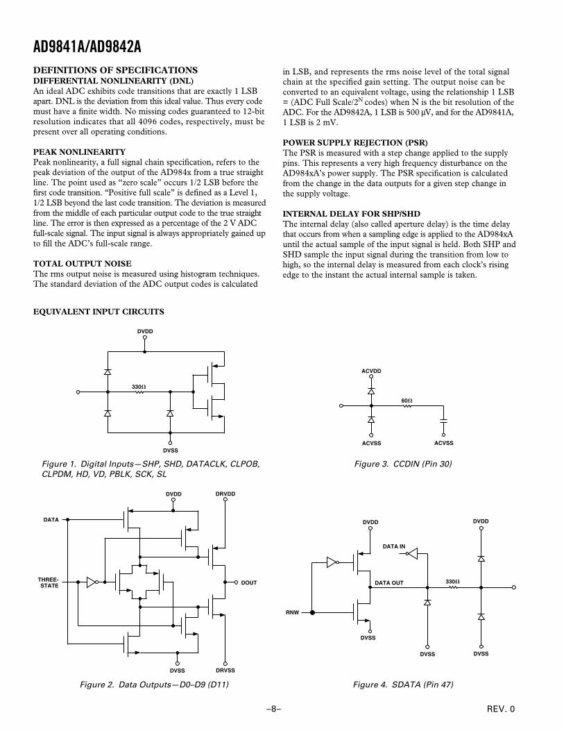
DEFINITIONS OF SPECIFICATIONSDIFFERENTIAL NONLINEARITY (DNL)An ideal ADC exhibits code transitions that are exactly 1 LSBapart. DNL is the deviation from this ideal value. Thus every codemust have a finite width. No missing codes guaranteed to 12-bitresolution indicates that all 4096 codes, respectively, must bepresent over all operating conditions.
PEAK NONLINEARITYPeak nonlinearity, a full signal chain specification, refers to thepeak deviation of the output of the AD984x from a true straightline. The point used as “zero scale” occurs 1/2 LSB before thefirst code transition. “Positive full scale” is defined as a Level 1,1/2 LSB beyond the last code transition. The deviation is measuredfrom the middle of each particular output code to the true straightline. The error is then expressed as a percentage of the 2 V ADCfull-scale signal. The input signal is always appropriately gained upto fill the ADC’s full-scale range.
TOTAL OUTPUT NOISEThe rms output noise is measured using histogram techniques.The standard deviation of the ADC output codes is calculated
in LSB, and represents the rms noise level of the total signalchain at the specified gain setting. The output noise can beconverted to an equivalent voltage, using the relationship 1 LSB= (ADC Full Scale/2N codes) when N is the bit resolution of theADC. For the AD9842A, 1 LSB is 500 µV, and for the AD9841A,1 LSB is 2 mV.
POWER SUPPLY REJECTION (PSR)The PSR is measured with a step change applied to the supplypins. This represents a very high frequency disturbance on theAD984xA’s power supply. The PSR specification is calculatedfrom the change in the data outputs for a given step change inthe supply voltage.
INTERNAL DELAY FOR SHP/SHDThe internal delay (also called aperture delay) is the time delaythat occurs from when a sampling edge is applied to the AD984xAuntil the actual sample of the input signal is held. Both SHP andSHD sample the input signal during the transition from low tohigh, so the internal delay is measured from each clock’s risingedge to the instant the actual internal sample is taken.
EQUIVALENT INPUT CIRCUITS
330�
DVDD
DVSS
Figure 1. Digital Inputs—SHP, SHD, DATACLK, CLPOB,CLPDM, HD, VD, PBLK, SCK, SL
DVDD
DVSS DRVSS
DRVDD
THREE-STATE
DATA
DOUT
Figure 2. Data Outputs—D0–D9 (D11)
60�
ACVDD
ACVSS ACVSS
Figure 3. CCDIN (Pin 30)
330�
DVDD
DVSS
DVDD
DVSS
DVSS
DATA IN
RNW
DATA OUT
Figure 4. SDATA (Pin 47)
REV. 0
AD9841A/AD9842A
–9–
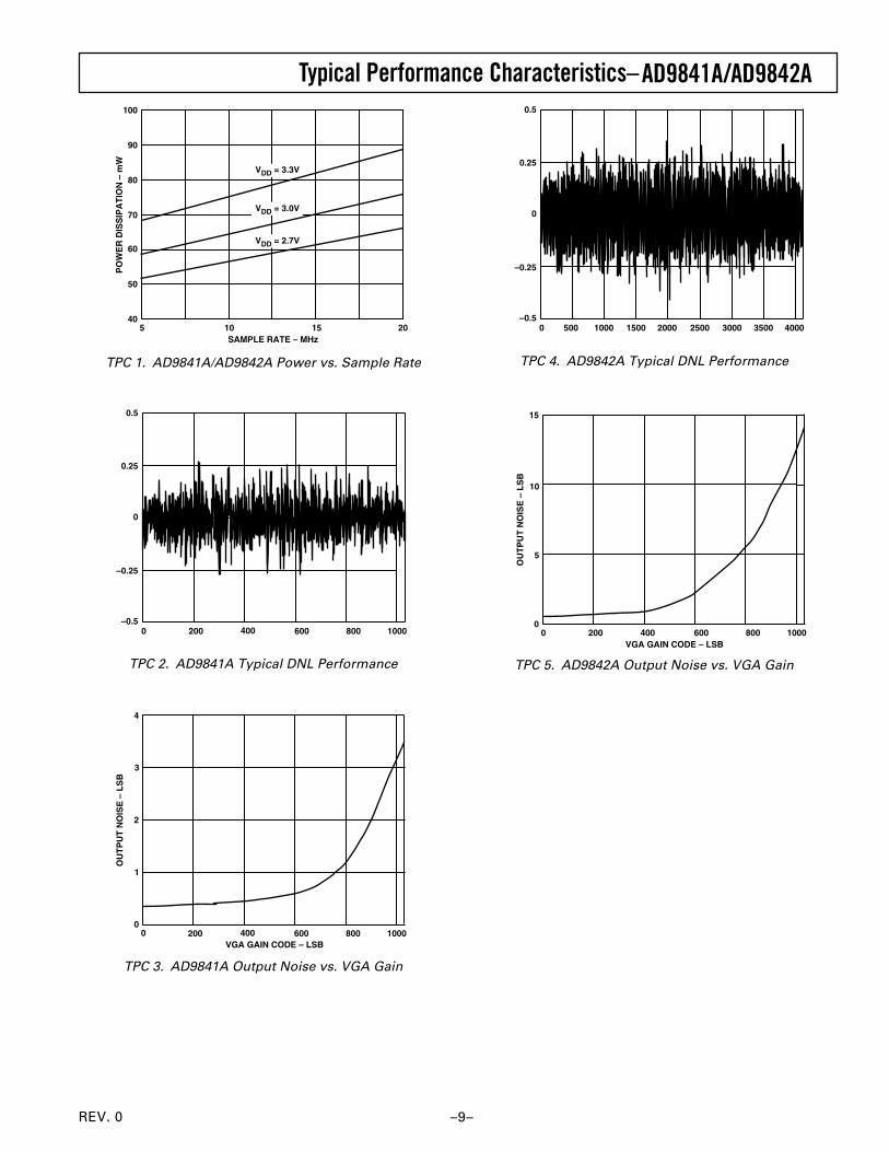
Typical Performance Characteristics–
SAMPLE RATE – MHz
100
70
405 2010
PO
WE
R D
ISS
IPA
TIO
N –
mW
50
60
80
90
15
VDD = 3.3V
VDD = 3.0V
VDD = 2.7V
TPC 1. AD9841A/AD9842A Power vs. Sample Rate
0 1000400200 600 800
0
–0.5
0.5
–0.25
0.25
TPC 2. AD9841A Typical DNL Performance
VGA GAIN CODE – LSB
4
2
00 1000400
OU
TP
UT
NO
ISE
– L
SB
200
1
600
3
800
TPC 3. AD9841A Output Noise vs. VGA Gain
0 1000500 1500 2000 2500 3000 3500 4000
0
–0.5
0.5
–0.25
0.25
TPC 4. AD9842A Typical DNL Performance
VGA GAIN CODE – LSB
15
00 1000400
OU
TP
UT
NO
ISE
– L
SB
200
5
600
10
800
TPC 5. AD9842A Output Noise vs. VGA Gain
REV. 0
AD9841A/AD9842A
–10–
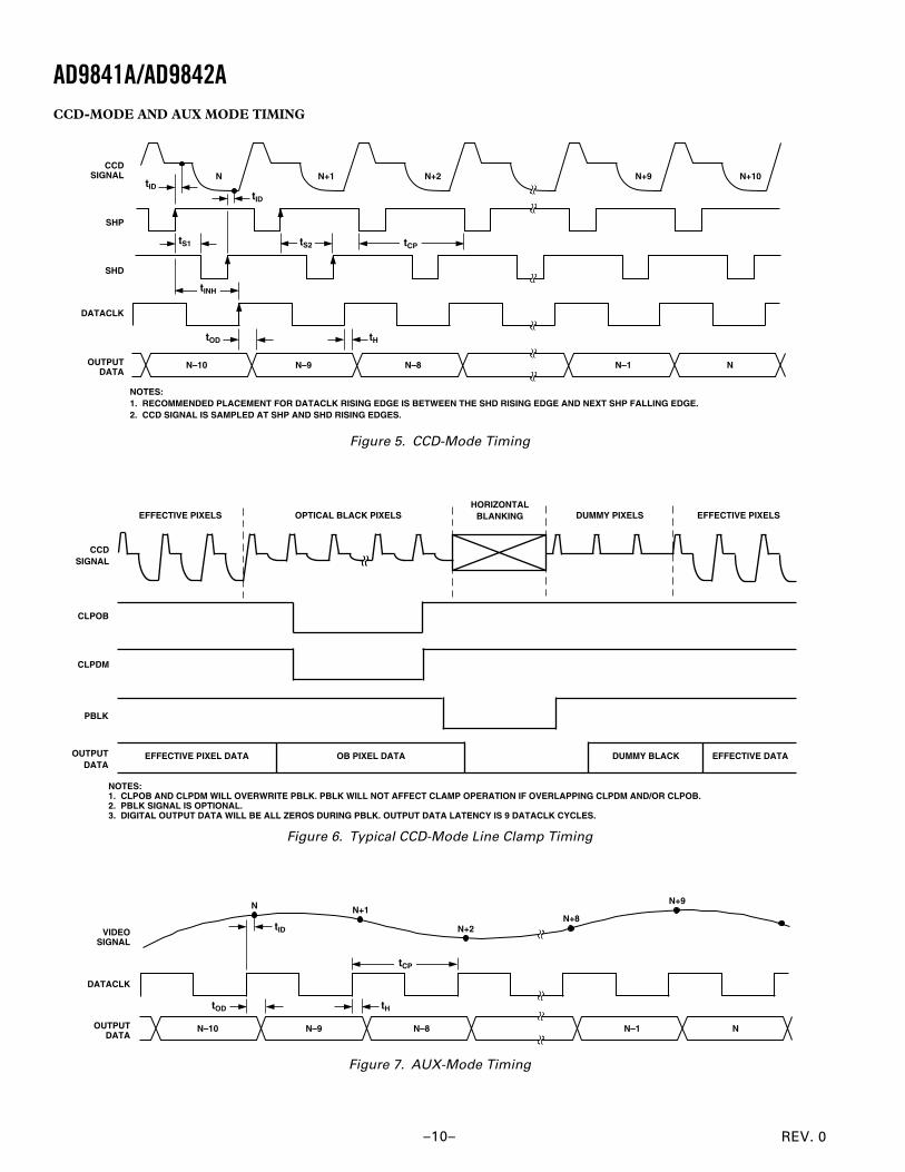
CCD-MODE AND AUX MODE TIMING
N N+1 N+2 N+9 N+10tID
tID
tS1 tS2 tCP
tINH
tOD tH
N–10 N–9 N–8 N–1 N
NOTES:1. RECOMMENDED PLACEMENT FOR DATACLK RISING EDGE IS BETWEEN THE SHD RISING EDGE AND NEXT SHP FALLING EDGE.2. CCD SIGNAL IS SAMPLED AT SHP AND SHD RISING EDGES.
SHP
SHD
DATACLK
OUTPUTDATA
CCDSIGNAL
Figure 5. CCD-Mode Timing
CCDSIGNAL
EFFECTIVE PIXELS
CLPOB
CLPDM
OPTICAL BLACK PIXELSHORIZONTAL
BLANKING DUMMY PIXELS EFFECTIVE PIXELS
PBLK
NOTES:1. CLPOB AND CLPDM WILL OVERWRITE PBLK. PBLK WILL NOT AFFECT CLAMP OPERATION IF OVERLAPPING CLPDM AND/OR CLPOB.2. PBLK SIGNAL IS OPTIONAL.3. DIGITAL OUTPUT DATA WILL BE ALL ZEROS DURING PBLK. OUTPUT DATA LATENCY IS 9 DATACLK CYCLES.
OUTPUTDATA
EFFECTIVE PIXEL DATA OB PIXEL DATA DUMMY BLACK EFFECTIVE DATA
Figure 6. Typical CCD-Mode Line Clamp Timing
DATACLK
OUTPUTDATA
VIDEOSIGNAL
N N+1
N+2N+8
N+9
N–10 N–9 N–8 N–1 N
tID
tCP
tOD tH
Figure 7. AUX-Mode Timing
REV. 0
AD9841A/AD9842A
–11–
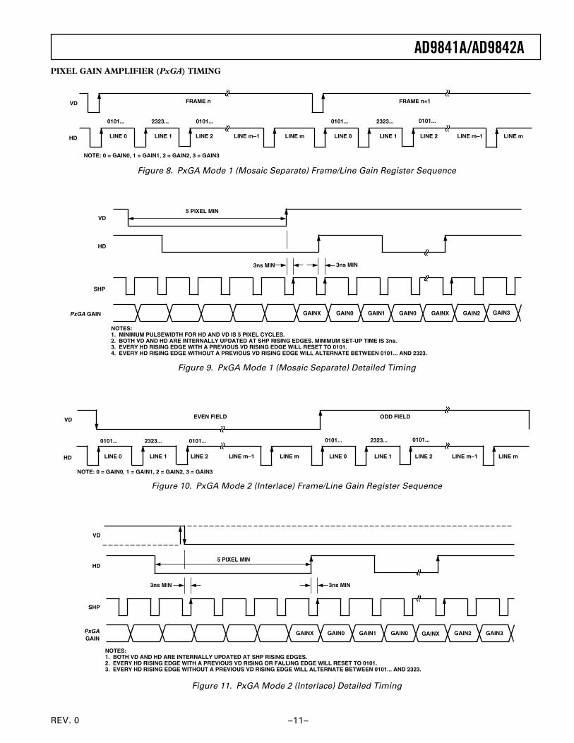
PIXEL GAIN AMPLIFIER (PxGA) TIMING
FRAME nVD
HD
FRAME n+1
LINE 0 LINE 1 LINE 2 LINE m
0101... 2323... 0101...
LINE m–1 LINE 0 LINE 1 LINE 2 LINE m
0101... 2323... 0101...
LINE m–1
NOTE: 0 = GAIN0, 1 = GAIN1, 2 = GAIN2, 3 = GAIN3
Figure 8. PxGA Mode 1 (Mosaic Separate) Frame/Line Gain Register Sequence
SHP
HD
PxGA GAIN
3ns MIN
GAIN0
VD
3ns MIN
GAIN1 GAIN0
NOTES:1. MINIMUM PULSEWIDTH FOR HD AND VD IS 5 PIXEL CYCLES.2. BOTH VD AND HD ARE INTERNALLY UPDATED AT SHP RISING EDGES. MINIMUM SET-UP TIME IS 3ns.3. EVERY HD RISING EDGE WITH A PREVIOUS VD RISING EDGE WILL RESET TO 0101.4. EVERY HD RISING EDGE WITHOUT A PREVIOUS VD RISING EDGE WILL ALTERNATE BETWEEN 0101... AND 2323.
GAIN3GAIN2GAINXGAINX
5 PIXEL MIN
Figure 9. PxGA Mode 1 (Mosaic Separate) Detailed Timing
EVEN FIELD ODD FIELD
0101... 2323... 0101...
NOTE: 0 = GAIN0, 1 = GAIN1, 2 = GAIN2, 3 = GAIN3
0101... 2323... 0101...
HD LINE 0 LINE 1 LINE 2 LINE mLINE m–1 LINE 0 LINE 1 LINE 2 LINE mLINE m–1
VD
Figure 10. PxGA Mode 2 (Interlace) Frame/Line Gain Register Sequence
SHP
HD
PxGAGAIN
3ns MIN
GAIN0
3ns MIN
GAIN1 GAIN0 GAIN3GAIN2GAINXGAINX
5 PIXEL MIN
VD
NOTES:1. BOTH VD AND HD ARE INTERNALLY UPDATED AT SHP RISING EDGES.2. EVERY HD RISING EDGE WITH A PREVIOUS VD RISING OR FALLING EDGE WILL RESET TO 0101.3. EVERY HD RISING EDGE WITHOUT A PREVIOUS VD RISING EDGE WILL ALTERNATE BETWEEN 0101... AND 2323.
Figure 11. PxGA Mode 2 (Interlace) Detailed Timing
REV. 0
AD9841A/AD9842A
–12–
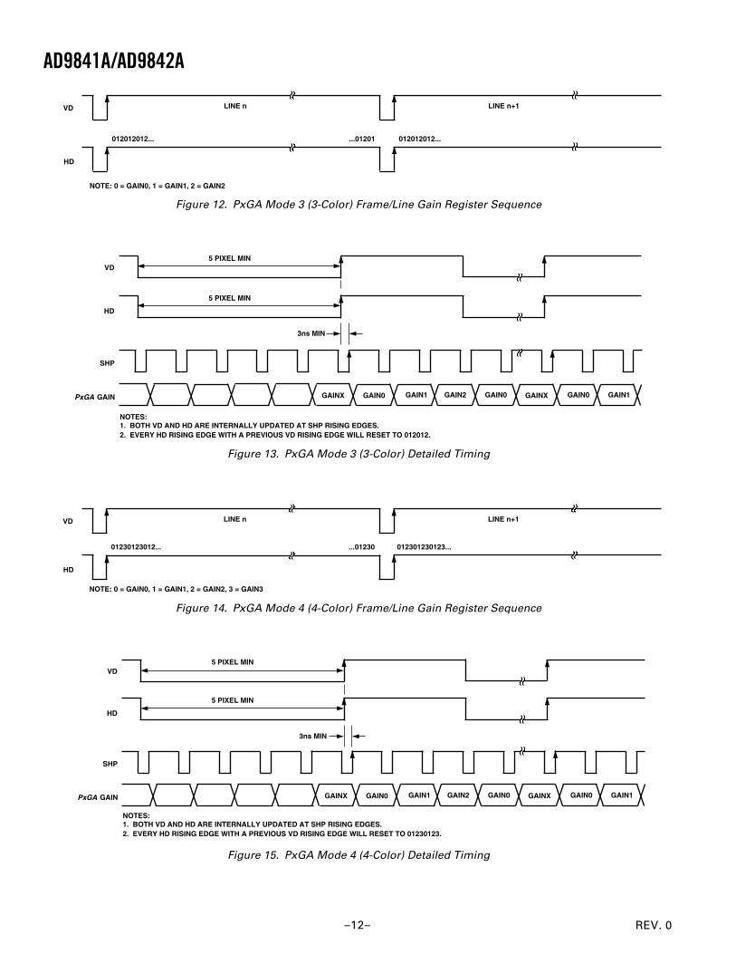
VD
HD
NOTE: 0 = GAIN0, 1 = GAIN1, 2 = GAIN2
LINE n LINE n+1
012012012... 012012012......01201
Figure 12. PxGA Mode 3 (3-Color) Frame/Line Gain Register Sequence
SHP
HD
PxGA GAIN GAIN1
VD
GAIN2 GAIN0 GAIN1GAIN0GAINXGAIN0GAINX
3ns MIN
5 PIXEL MIN
5 PIXEL MIN
NOTES:1. BOTH VD AND HD ARE INTERNALLY UPDATED AT SHP RISING EDGES.2. EVERY HD RISING EDGE WITH A PREVIOUS VD RISING EDGE WILL RESET TO 012012.
Figure 13. PxGA Mode 3 (3-Color) Detailed Timing
VD
HD
NOTE: 0 = GAIN0, 1 = GAIN1, 2 = GAIN2, 3 = GAIN3
LINE n LINE n+1
012301230123......0123001230123012...
Figure 14. PxGA Mode 4 (4-Color) Frame/Line Gain Register Sequence
SHP
HD
PxGA GAIN GAIN1
VD
GAIN2 GAIN0 GAIN1GAIN0GAINXGAIN0GAINX
3ns MIN
5 PIXEL MIN
5 PIXEL MIN
NOTES:1. BOTH VD AND HD ARE INTERNALLY UPDATED AT SHP RISING EDGES.2. EVERY HD RISING EDGE WITH A PREVIOUS VD RISING EDGE WILL RESET TO 01230123.
Figure 15. PxGA Mode 4 (4-Color) Detailed Timing
REV. 0
AD9841A/AD9842A
–13–
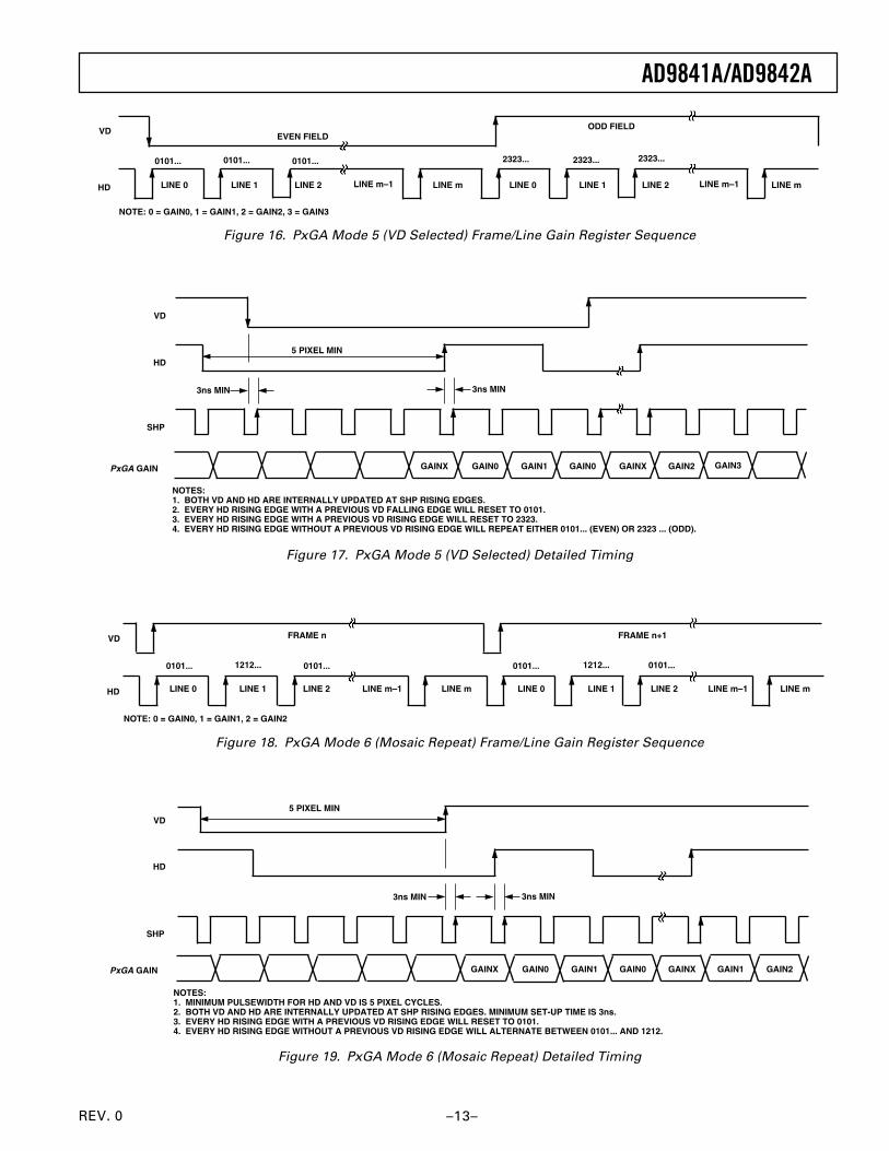
EVEN FIELDODD FIELD
0101... 0101... 0101...
NOTE: 0 = GAIN0, 1 = GAIN1, 2 = GAIN2, 3 = GAIN3
2323... 2323... 2323...
HD LINE 0 LINE 1 LINE 2 LINE mLINE m–1 LINE 0 LINE 1 LINE 2 LINE mLINE m–1
VD
Figure 16. PxGA Mode 5 (VD Selected) Frame/Line Gain Register Sequence
SHP
HD
PxGA GAIN
3ns MIN
GAIN0
VD
GAIN1 GAIN0
NOTES:1. BOTH VD AND HD ARE INTERNALLY UPDATED AT SHP RISING EDGES.2. EVERY HD RISING EDGE WITH A PREVIOUS VD FALLING EDGE WILL RESET TO 0101.3. EVERY HD RISING EDGE WITH A PREVIOUS VD RISING EDGE WILL RESET TO 2323.4. EVERY HD RISING EDGE WITHOUT A PREVIOUS VD RISING EDGE WILL REPEAT EITHER 0101... (EVEN) OR 2323 ... (ODD).
GAIN3GAIN2GAINXGAINX
5 PIXEL MIN
3ns MIN
Figure 17. PxGA Mode 5 (VD Selected) Detailed Timing
FRAME nVD
HD
FRAME n+1
LINE 0 LINE 1 LINE 2 LINE m
0101... 1212... 0101...
LINE m–1 LINE 0 LINE 1 LINE 2 LINE m
0101... 1212... 0101...
LINE m–1
NOTE: 0 = GAIN0, 1 = GAIN1, 2 = GAIN2
Figure 18. PxGA Mode 6 (Mosaic Repeat) Frame/Line Gain Register Sequence
SHP
HD
PxGA GAIN
3ns MIN
GAIN0
VD
3ns MIN
GAIN1 GAIN0
NOTES:1. MINIMUM PULSEWIDTH FOR HD AND VD IS 5 PIXEL CYCLES.2. BOTH VD AND HD ARE INTERNALLY UPDATED AT SHP RISING EDGES. MINIMUM SET-UP TIME IS 3ns.3. EVERY HD RISING EDGE WITH A PREVIOUS VD RISING EDGE WILL RESET TO 0101.4. EVERY HD RISING EDGE WITHOUT A PREVIOUS VD RISING EDGE WILL ALTERNATE BETWEEN 0101... AND 1212.
GAIN2GAINXGAINX
5 PIXEL MIN
GAIN1
Figure 19. PxGA Mode 6 (Mosaic Repeat) Detailed Timing
REV. 0
AD9841A/AD9842A
–14–
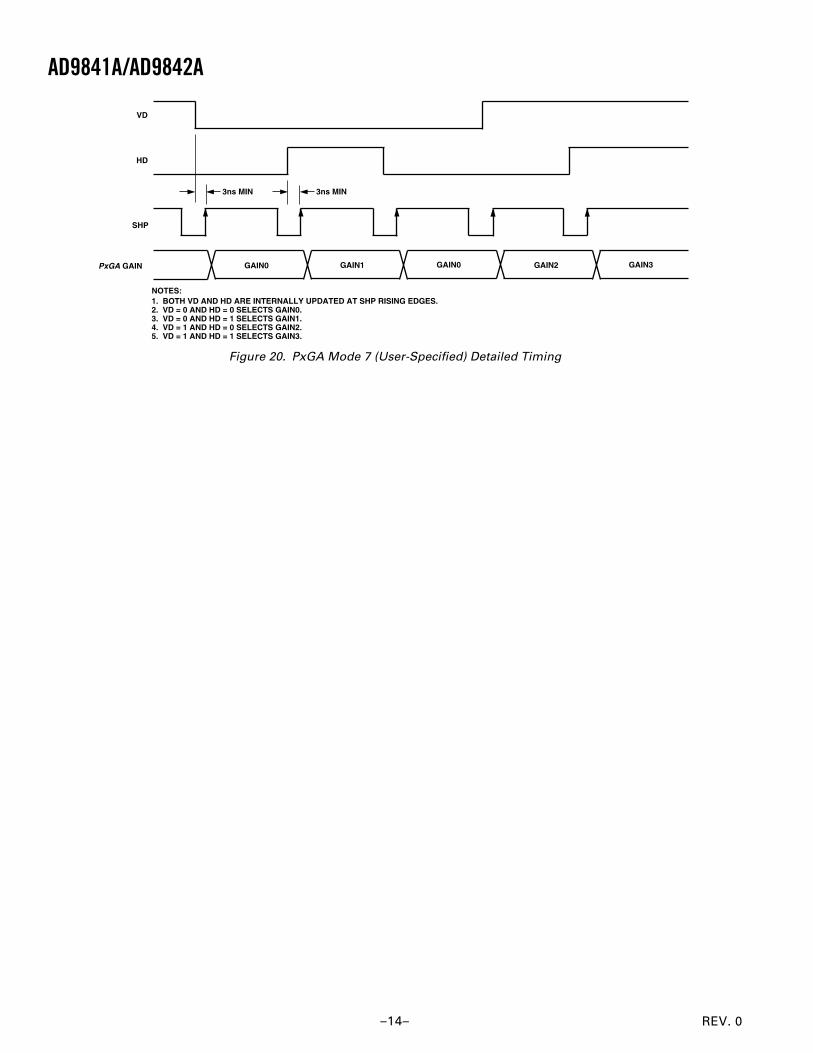
SHP
HD
3ns MIN
GAIN1
VD
GAIN0 GAIN2 GAIN3
3ns MIN
1. BOTH VD AND HD ARE INTERNALLY UPDATED AT SHP RISING EDGES.2. VD = 0 AND HD = 0 SELECTS GAIN0.3. VD = 0 AND HD = 1 SELECTS GAIN1.4. VD = 1 AND HD = 0 SELECTS GAIN2.5. VD = 1 AND HD = 1 SELECTS GAIN3.
GAIN0PxGA GAIN
NOTES:
Figure 20. PxGA Mode 7 (User-Specified) Detailed Timing
REV. 0
AD9841A/AD9842A
–15–
SDATA
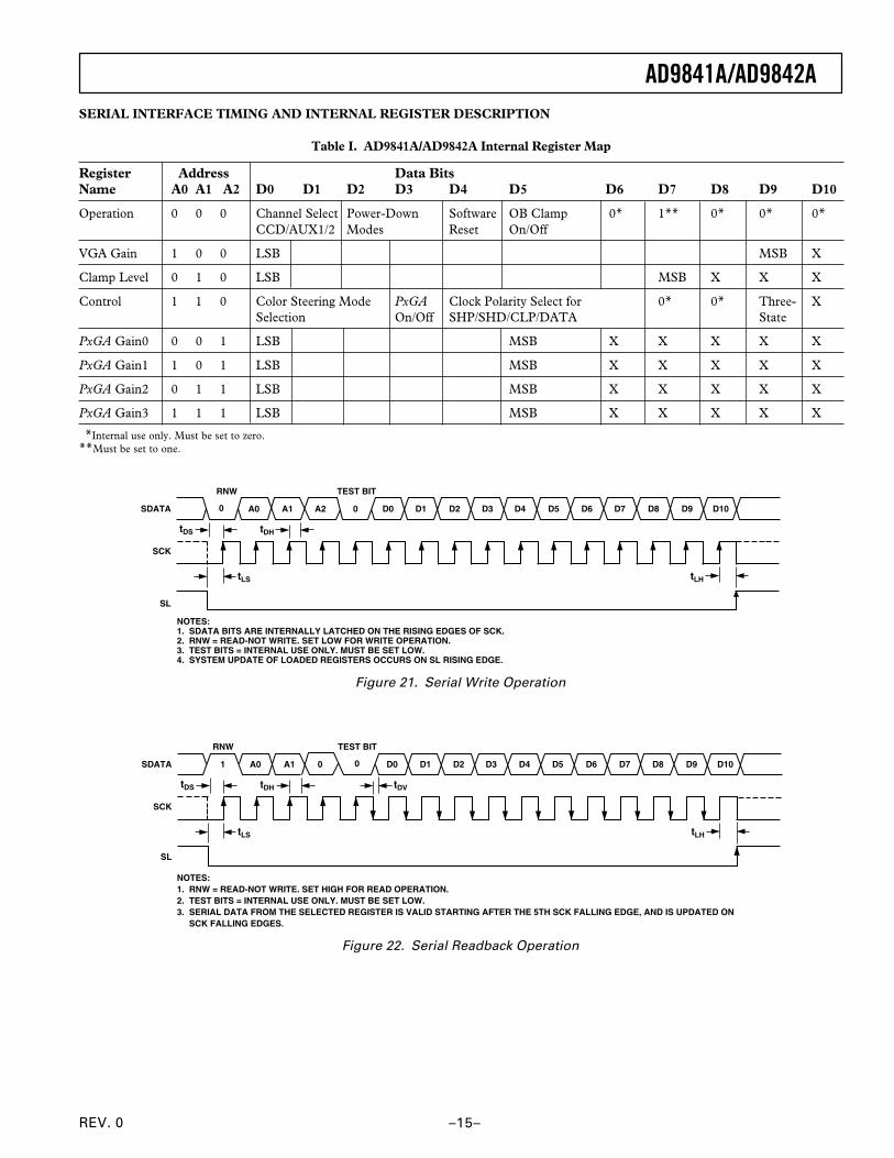
SCK
SL
RNW TEST BIT
0 A2 0A0 A1 D0 D1 D2 D3 D4 D5 D6 D7 D8 D9 D10
tDS tDH
tLS tLH
NOTES:1. SDATA BITS ARE INTERNALLY LATCHED ON THE RISING EDGES OF SCK.2. RNW = READ-NOT WRITE. SET LOW FOR WRITE OPERATION.3. TEST BITS = INTERNAL USE ONLY. MUST BE SET LOW.4. SYSTEM UPDATE OF LOADED REGISTERS OCCURS ON SL RISING EDGE.
Figure 21. Serial Write Operation
SDATA
SCK
SL
RNW TEST BIT
1 0 0A0 A1 D0 D1 D2 D3 D4 D5 D6 D7 D8 D9 D10
tDS tDH
tLS tLH
NOTES:1. RNW = READ-NOT WRITE. SET HIGH FOR READ OPERATION.2. TEST BITS = INTERNAL USE ONLY. MUST BE SET LOW.3. SERIAL DATA FROM THE SELECTED REGISTER IS VALID STARTING AFTER THE 5TH SCK FALLING EDGE, AND IS UPDATED ON SCK FALLING EDGES.
tDV
Figure 22. Serial Readback Operation
SERIAL INTERFACE TIMING AND INTERNAL REGISTER DESCRIPTION
Table I. AD9841A/AD9842A Internal Register Map
Register Address Data BitsName A0 A1 A2 D0 D1 D2 D3 D4 D5 D6 D7 D8 D9 D10
Operation 0 0 0 Channel Select Power-Down Software OB Clamp 0* 1** 0* 0* 0*CCD/AUX1/2 Modes Reset On/Off
VGA Gain 1 0 0 LSB MSB X
Clamp Level 0 1 0 LSB MSB X X X
Control 1 1 0 Color Steering Mode PxGA Clock Polarity Select for 0* 0* Three- XSelection On/Off SHP/SHD/CLP/DATA State
PxGA Gain0 0 0 1 LSB MSB X X X X X
PxGA Gain1 1 0 1 LSB MSB X X X X X
PxGA Gain2 0 1 1 LSB MSB X X X X X
PxGA Gain3 1 1 1 LSB MSB X X X X X
*Internal use only. Must be set to zero.**Must be set to one.

REV. 0
AD9841A/AD9842A
–16–
SDATA
SCK
SL
A0 A1 A2
D0 D10 D0 D9 D0 D0D7
RNW
00 D900 0 D0
1 2 17 35342726166543 44 45 51 6362575650 68
... ............ .........
10 BITSACG GAIN
D5 D0 D5 D0 D0D5 D5
...
...... ... ... ... ... ... ...
NOTES:1. ANY NUMBER OF ADJACENT REGISTERS MAY BE LOADED SEQUENTIALLY, BEGINNING WITH THE LOWEST ADDRESS AND INCREMENTING ONE ADDRESS AT A TIME.2. WHEN SEQUENTIALLY LOADING MULTIPLE REGISTERS, THE EXACT REGISTER LENGTH (SHOWN ABOVE) MUST BE USED FOR EACH REGISTER.3. ALL LOADED REGISTERS WILL BE SIMULTANEOUSLY UPDATED WITH THE RISING EDGE OF SL.
8 BITSCLAMP LEVEL
10 BITSCONTROL
11 BITSOPERATION
6 BITSPxGA GAIN0
6 BITSPxGA GAIN1
6 BITSPxGA GAIN2
6 BITSPxGA GAIN3
Figure 23. Continuous Serial Write Operation to All Registers
SDATA
A0 A1 A2
D1D0 D1 D2 D3 D4 D5 D0 D3D2 D400
23 241 2 17161514131211109876543 2918
... ...
D500 1 D5D5D0 D0
RNW
SCK
SL
PxGA GAIN0 PxGA GAIN1 PxGA GAIN3PxGA GAIN2
...
......
Figure 24. Continuous Serial Write Operation to All PxGA Gain Registers
Table II. Operation Register Contents (Default Value x000)
Optical Black Clamp Reset Power-Down Modes Channel Selection D10 D9 D8 D7 D6 D5 D4 D3 D2 D1 D0
0* 0* 0* 1** 0* 0 Enable Clamping 0 Normal 0 0 Normal Power 0 0 CCD Mode1 Disable Clamping 1 Reset All Registers 0 1 Fast Recovery 0 1 AUX1 Mode
to Default 1 0 Standby 1 0 AUX2 Mode1 1 Total Power-Down 1 1 Test Only
*Must be set to zero.**Set to one.
Table III. VGA Gain Register Contents (Default Value x096)
MSB LSBD10 D9 D8 D7 D6 D5 D4 D3 D2 D1 D0 Gain (dB)
X 0 0 0 1 0 1 1 1 1 1 2.0• •• •• •
1 1 1 1 1 1 1 1 1 0 35.9651 1 1 1 1 1 1 1 1 1 36.0
REV. 0
AD9841A/AD9842A
–17–
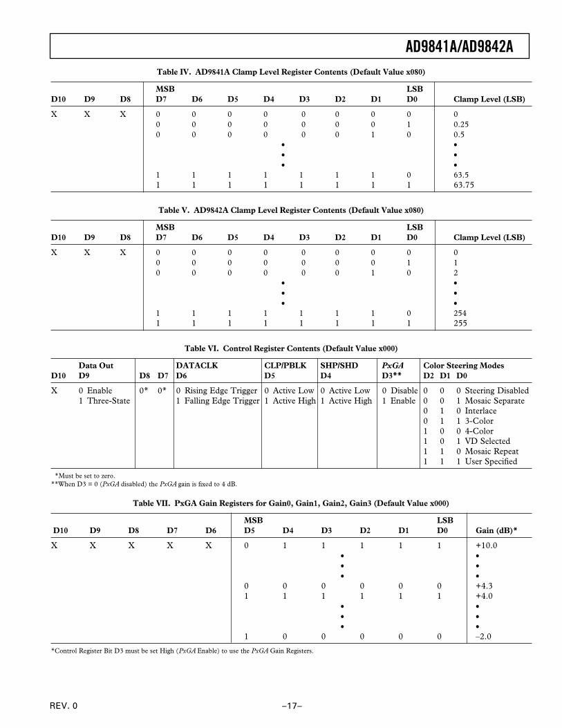
Table IV. AD9841A Clamp Level Register Contents (Default Value x080)
MSB LSBD10 D9 D8 D7 D6 D5 D4 D3 D2 D1 D0 Clamp Level (LSB)
X X X 0 0 0 0 0 0 0 0 00 0 0 0 0 0 0 1 0.250 0 0 0 0 0 1 0 0.5
• • • • • •
1 1 1 1 1 1 1 0 63.51 1 1 1 1 1 1 1 63.75
Table V. AD9842A Clamp Level Register Contents (Default Value x080)
MSB LSBD10 D9 D8 D7 D6 D5 D4 D3 D2 D1 D0 Clamp Level (LSB)
X X X 0 0 0 0 0 0 0 0 00 0 0 0 0 0 0 1 10 0 0 0 0 0 1 0 2
• • • • • •
1 1 1 1 1 1 1 0 2541 1 1 1 1 1 1 1 255
Table VI. Control Register Contents (Default Value x000)
Data Out DATACLK CLP/PBLK SHP/SHD PxGA Color Steering ModesD10 D9 D8 D7 D6 D5 D4 D3** D2 D1 D0
X 0 Enable 0* 0* 0 Rising Edge Trigger 0 Active Low 0 Active Low 0 Disable 0 0 0 Steering Disabled1 Three-State 1 Falling Edge Trigger 1 Active High 1 Active High 1 Enable 0 0 1 Mosaic Separate
0 1 0 Interlace0 1 1 3-Color1 0 0 4-Color1 0 1 VD Selected1 1 0 Mosaic Repeat1 1 1 User Specified
*Must be set to zero.**When D3 = 0 (PxGA disabled) the PxGA gain is fixed to 4 dB.
Table VII. PxGA Gain Registers for Gain0, Gain1, Gain2, Gain3 (Default Value x000)
MSB LSB D10 D9 D8 D7 D6 D5 D4 D3 D2 D1 D0 Gain (dB)*
X X X X X 0 1 1 1 1 1 +10.0• •• •• •
0 0 0 0 0 0 +4.31 1 1 1 1 1 +4.0
• •• •• •
1 0 0 0 0 0 –2.0
*Control Register Bit D3 must be set High (PxGA Enable) to use the PxGA Gain Registers.
REV. 0
AD9841A/AD9842A
–18–
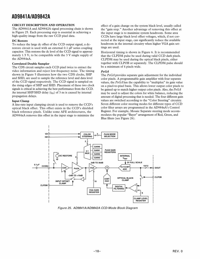
CIRCUIT DESCRIPTION AND OPERATIONThe AD9841A and AD9842A signal processing chain is shownin Figure 25. Each processing step is essential in achieving ahigh-quality image from the raw CCD pixel data.
DC RestoreTo reduce the large dc offset of the CCD output signal, a dc-restore circuit is used with an external 0.1 µF series couplingcapacitor. This restores the dc level of the CCD signal to approxi-mately 1.5 V, to be compatible with the 3 V single supply ofthe AD984xA.
Correlated Double SamplerThe CDS circuit samples each CCD pixel twice to extract thevideo information and reject low-frequency noise. The timingshown in Figure 5 illustrates how the two CDS clocks, SHPand SHD, are used to sample the reference level and data levelof the CCD signal respectively. The CCD signal is sampled onthe rising edges of SHP and SHD. Placement of these two clocksignals is critical in achieving the best performance from the CCD.An internal SHP/SHD delay (tID) of 3 ns is caused by internalpropagation delays.
Input ClampA line-rate input clamping circuit is used to remove the CCD’soptical black offset. This offset exists in the CCD’s shieldedblack reference pixels. Unlike some AFE architectures, theAD984xA removes this offset in the input stage to minimize the
effect of a gain change on the system black level, usually calledthe “gain step.” Another advantage of removing this offset atthe input stage is to maximize system headroom. Some areaCCDs have large black level offset voltages, which, if not cor-rected at the input stage, can significantly reduce the availableheadroom in the internal circuitry when higher VGA gain set-tings are used.
Horizontal timing is shown in Figure 6. It is recommendedthat the CLPDM pulse be used during valid CCD dark pixels.CLPDM may be used during the optical black pixels, eithertogether with CLPOB or separately. The CLPDM pulse shouldbe a minimum of 4 pixels wide.
PxGAThe PxGA provides separate gain adjustment for the individualcolor pixels. A programmable gain amplifier with four separatevalues, the PxGA has the capability to “multiplex” its gain valueon a pixel-to-pixel basis. This allows lower output color pixels tobe gained up to match higher output color pixels. Also, the PxGAmay be used to adjust the colors for white balance, reducing theamount of digital processing that is needed. The four different gainvalues are switched according to the “Color Steering” circuitry.Seven different color steering modes for different types of CCDcolor filter arrays are programmed in the AD984xA’s ControlRegister. For example, Mosaic Separate steering mode accom-modates the popular “Bayer” arrangement of Red, Green, andBlue filters (see Figure 26).
2dB TO 36dB
CLPDM
CCDIN
DIGITALFILTERING
CLPOB
DC RESTORE
OPTICAL BLACKCLAMP
0.1�F
DOUT10-/12-BITADC
VGA
8-BITDAC
CLAMP LEVELREGISTER
8VGA GAINREGISTER
10
CDS
INPUT OFFSETCLAMP
INTERNALVREF
2V FULL SCALE
COLORSTEERING
4:1MUX
3
GAIN0
GAIN1
GAIN2
GAIN3
PxGA
–2dB TO +10dB
PxGA MODESELECTION
2
6
VD
HD
PxGA GAINREGISTERS
10/12
Figure 25. AD9841A/AD9842A CCD-Mode Block Diagram
REV. 0
AD9841A/AD9842A
–19–
R R
Gb Gb
GrGr
B B
CCD: PROGRESSIVE BAYER
LINE0 GAIN0, GAIN1, GAIN0, GAIN1 ...
R R GrGr
Gb GbB B
LINE1
LINE2
GAIN2, GAIN3, GAIN2, GAIN3 ...
GAIN0, GAIN1, GAIN0, GAIN1 ...
MOSAIC SEPARATE COLORSTEERING MODE
Figure 26. CCD Color Filter Example: Progressive Scan
LINE0 GAIN0, GAIN1, GAIN0, GAIN1 ...
R R GrGr
LINE1
LINE2
GAIN0, GAIN1, GAIN0, GAIN1 ...
GAIN0, GAIN1, GAIN0, GAIN1 ...
Gb GbB B
LINE0 GAIN2, GAIN3, GAIN2, GAIN3 ...
LINE1
LINE2
GAIN2, GAIN3, GAIN2, GAIN3 ...
GAIN2, GAIN3, GAIN2, GAIN3 ...
CCD: INTERLACED BAYER EVEN FIELD
VD SELECTED COLORSTEERING MODE
ODD FIELD
Gb GbB B
Gb GbB B
Gb GbB B
R R GrGr
R R GrGr
R R GrGr
Figure 27. CCD Color Filter Example: Interlaced
The same Bayer pattern can also be interlaced, and the VDSelected mode should be used with this type of CCD (see Fig-ure 27). The Color Steering performs the proper multiplexing ofthe R, G, and B gain values (loaded into the PxGA gain regis-ters), and is synchronized by the user with vertical (VD) andhorizontal (HD) sync pulses. For more detailed information, seethe PxGA Timing section. The PxGA gain for each of the fourchannels is variable from –2 dB to +10 dB, controlled in 64 stepsthrough the serial interface. The PxGA gain curve is shown inFigure 28.
PxGA GAIN REGISTER CODE
10
32
PxG
A G
AIN
– d
B
40 48 56 0 8 16 24 31
8
6
4
2
0
-2
(100000) (011111)
Figure 28. PxGA Gain Curve
Variable Gain AmplifierThe VGA stage provides a gain range of 2 dB to 36 dB, program-mable with 10-bit resolution through the serial digital interface.Combined with 4 dB from the PxGA stage, the total gain rangefor the AD984xA is 6 dB to 40 dB. The minimum gain of 6 dB
is needed to match a 1 V input signal with the ADC full-scalerange of 2 V. When compared to 1 V full-scale systems (such asADI’s AD9803), the equivalent gain range is 0 dB to 34 dB.
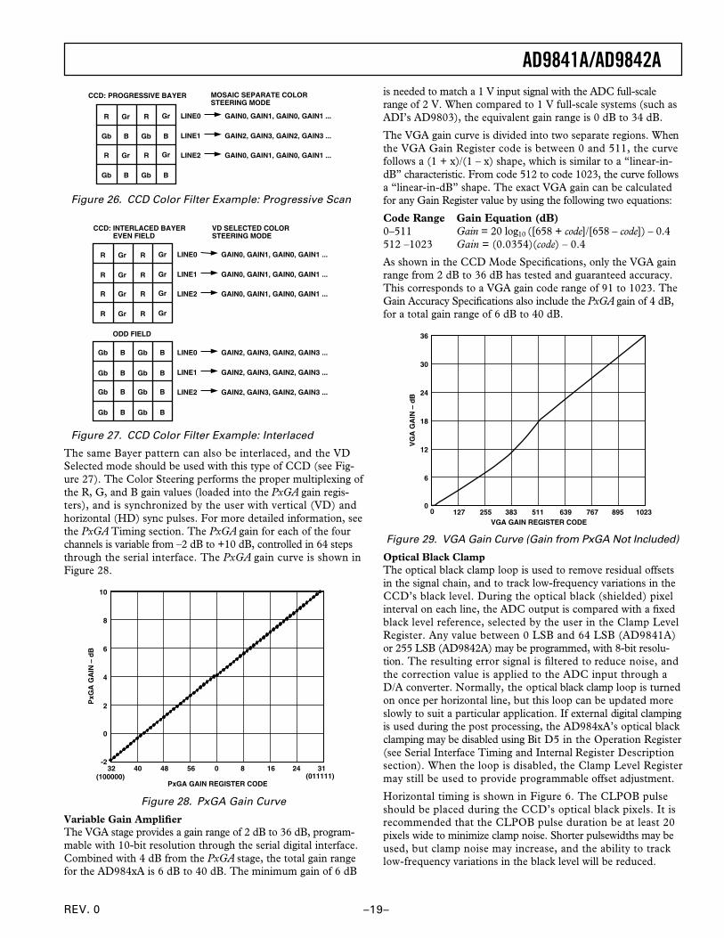
The VGA gain curve is divided into two separate regions. Whenthe VGA Gain Register code is between 0 and 511, the curvefollows a (1 + x)/(1 – x) shape, which is similar to a “linear-in-dB” characteristic. From code 512 to code 1023, the curve followsa “linear-in-dB” shape. The exact VGA gain can be calculatedfor any Gain Register value by using the following two equations:
Code Range Gain Equation (dB)0–511 Gain = 20 log10 ([658 + code]/[658 – code]) – 0.4512 –1023 Gain = (0.0354)(code) – 0.4
As shown in the CCD Mode Specifications, only the VGA gainrange from 2 dB to 36 dB has tested and guaranteed accuracy.This corresponds to a VGA gain code range of 91 to 1023. TheGain Accuracy Specifications also include the PxGA gain of 4 dB,for a total gain range of 6 dB to 40 dB.
VGA GAIN REGISTER CODE
36
0
VG
A G
AIN
– d
B
127 255 383 511 639 767 895 1023
30
24
18
12
6
0
Figure 29. VGA Gain Curve (Gain from PxGA Not Included)
Optical Black ClampThe optical black clamp loop is used to remove residual offsetsin the signal chain, and to track low-frequency variations in theCCD’s black level. During the optical black (shielded) pixelinterval on each line, the ADC output is compared with a fixedblack level reference, selected by the user in the Clamp LevelRegister. Any value between 0 LSB and 64 LSB (AD9841A)or 255 LSB (AD9842A) may be programmed, with 8-bit resolu-tion. The resulting error signal is filtered to reduce noise, andthe correction value is applied to the ADC input through aD/A converter. Normally, the optical black clamp loop is turnedon once per horizontal line, but this loop can be updated moreslowly to suit a particular application. If external digital clampingis used during the post processing, the AD984xA’s optical blackclamping may be disabled using Bit D5 in the Operation Register(see Serial Interface Timing and Internal Register Descriptionsection). When the loop is disabled, the Clamp Level Registermay still be used to provide programmable offset adjustment.
Horizontal timing is shown in Figure 6. The CLPOB pulseshould be placed during the CCD’s optical black pixels. It isrecommended that the CLPOB pulse duration be at least 20pixels wide to minimize clamp noise. Shorter pulsewidths may beused, but clamp noise may increase, and the ability to tracklow-frequency variations in the black level will be reduced.
REV. 0
AD9841A/AD9842A
–20–
A/D ConverterThe AD9841A and AD9842A use high-performance ADC archi-tectures, optimized for high speed and low power. DifferentialNonlinearity (DNL) performance is typically better than 0.5 LSB,as shown in TPCs 2 and 4. Instead of the 1 V full-scale rangeused by the earlier AD9801 and AD9803 products from AnalogDevices, the AD984xA ADCs use a 2 V input range. Betternoise performance results from using a larger ADC full-scalerange (see TPCs 3 and 5).
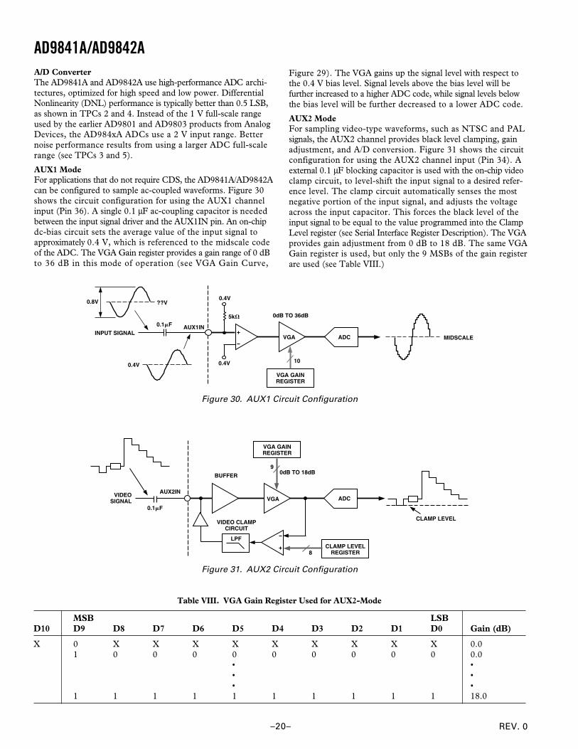
AUX1 ModeFor applications that do not require CDS, the AD9841A/AD9842Acan be configured to sample ac-coupled waveforms. Figure 30shows the circuit configuration for using the AUX1 channelinput (Pin 36). A single 0.1 µF ac-coupling capacitor is neededbetween the input signal driver and the AUX1IN pin. An on-chipdc-bias circuit sets the average value of the input signal toapproximately 0.4 V, which is referenced to the midscale codeof the ADC. The VGA Gain register provides a gain range of 0 dBto 36 dB in this mode of operation (see VGA Gain Curve,
Figure 29). The VGA gains up the signal level with respect tothe 0.4 V bias level. Signal levels above the bias level will befurther increased to a higher ADC code, while signal levels belowthe bias level will be further decreased to a lower ADC code.
AUX2 ModeFor sampling video-type waveforms, such as NTSC and PALsignals, the AUX2 channel provides black level clamping, gainadjustment, and A/D conversion. Figure 31 shows the circuitconfiguration for using the AUX2 channel input (Pin 34). Aexternal 0.1 µF blocking capacitor is used with the on-chip videoclamp circuit, to level-shift the input signal to a desired refer-ence level. The clamp circuit automatically senses the mostnegative portion of the input signal, and adjusts the voltageacross the input capacitor. This forces the black level of theinput signal to be equal to the value programmed into the ClampLevel register (see Serial Interface Register Description). The VGAprovides gain adjustment from 0 dB to 18 dB. The same VGAGain register is used, but only the 9 MSBs of the gain registerare used (see Table VIII.)
AUX1IN0.1�F
VGA GAINREGISTER
ADCVGA
10
5k�
0.4V
0.4V
INPUT SIGNAL
??V0.8V
0.4V
MIDSCALE
0dB TO 36dB
Figure 30. AUX1 Circuit Configuration
0dB TO 18dB
8
AUX2IN
BUFFER
0.1�F
VIDEOSIGNAL
9
CLAMP LEVEL
LPF
VGA GAINREGISTER
ADCVGA
VIDEO CLAMPCIRCUIT
CLAMP LEVELREGISTER
Figure 31. AUX2 Circuit Configuration
Table VIII. VGA Gain Register Used for AUX2-Mode
MSB LSBD10 D9 D8 D7 D6 D5 D4 D3 D2 D1 D0 Gain (dB)
X 0 X X X X X X X X X 0.01 0 0 0 0 0 0 0 0 0 0.0
• •• •• •
1 1 1 1 1 1 1 1 1 1 18.0
REV. 0
AD9841A/AD9842A
–21–
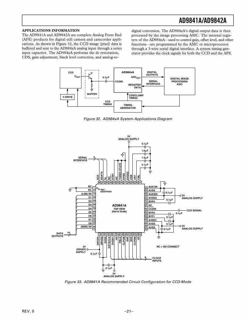
CCD
CCDIN
BUFFER
VOUT 0.1�F
AD984xA
ADCOUT
REGISTERDATA
SERIALINTERFACE
DIGITALOUTPUTS
DIGITAL IMAGEPROCESSING
ASIC
TIMINGGENERATOR
V-DRIVE
CCDTIMING
CDS/CLAMPTIMING
Figure 32. AD984xA System Applications Diagram
36
35
34
33
32
31
30
29
28
27
26
25
13 14 15 16 17 18 19 20 21 22 23 24
1
2
3
4
5
6
7
8
9
10
11
12
3748 47 46 45 44 39 3843 42 41 40
PIN 1IDENTIFIER
TOP VIEW(Not to Scale)
AUX1IN
AVSS
AUX2IN
AVDD2
BYP4
NC
CCDIN
BYP2
BYP1
AVDD1
AVSS
AVSS
NC
NC
(LSB) D0
D1
D2
D3
D4
D5
D6
D7
D8(MSB) D9
AD9841A
SC
K
SD
AT
A
SL
NC
ST
BY
NC
TH
RE
E-S
TA
TE
DV
SS
DV
DD
2
VR
B
VR
T
CM
L
DR
VD
D
DR
VS
S
DV
SS
DA
TA
CL
K
DV
DD
1
HD
PB
LK
CL
PO
B
SH
P
SH
D
CL
PD
M VD
0.1�F
0.1�F
0.1�F
0.1�F
0.1�F
0.1�F3VANALOG SUPPLY
CCD SIGNAL
3VANALOG SUPPLY
10DATAOUTPUTS
3SERIALINTERFACE
0.1�F
1.0�F
1.0�F
0.1�F
3VANALOG SUPPLY
8 CLOCKINPUTS
0.1�F
0.1�F
3VANALOG SUPPLY
3VDRIVERSUPPLY
NC = NO CONNECT
Figure 33. AD9841A Recommended Circuit Configuration for CCD-Mode
APPLICATIONS INFORMATIONThe AD9841A and AD9842A are complete Analog Front End(AFE) products for digital still camera and camcorder appli-cations. As shown in Figure 32, the CCD image (pixel) data isbuffered and sent to the AD984xA analog input through a seriesinput capacitor. The AD984xA performs the dc restoration,CDS, gain adjustment, black level correction, and analog-to-
digital conversion. The AD984xA’s digital output data is thenprocessed by the image processing ASIC. The internal regis-ters of the AD984xA—used to control gain, offset level, and otherfunctions—are programmed by the ASIC or microprocessorthrough a 3-wire serial digital interface. A system timing gen-erator provides the clock signals for both the CCD and the AFE.
REV. 0
AD9841A/AD9842A
–22–
36
35
34
33
32
31
30
29
28
27
26
25
13 14 15 16 17 18 19 20 21 22 23 24
1
2
3
4
5
6
7
8
9
10
11
12
3748 47 46 45 44 39 3843 42 41 40
PIN 1IDENTIFIER
TOP VIEW(Not to Scale)
AUX1IN
AVSS
AUX2IN
AVDD2
BYP4
NC
CCDIN
BYP2BYP1
AVDD1
AVSS
AVSS
D0
D1
D2D3
D4
D5D6
D7
D8
(MSB) D11
AD9842A
SC
K
SD
AT
A
SL
NC
ST
BY
NC
TH
RE
E-S
TA
TE
DV
SS
DV
DD
2V
RB
VR
T
CM
L
DR
VD
D
DR
VS
S
DV
SS
DA
TA
CL
K
DV
DD
1
HD
PB
LK
CL
PO
B
SH
P
SH
D
CL
PD
M VD
0.1�F
0.1�F
0.1�F
0.1�F
0.1�F
0.1�F3VANALOG SUPPLY
CCD SIGNAL
3VANALOG SUPPLY
12DATAOUTPUTS
3SERIALINTERFACE
0.1�F
1.0�F
1.0�F
0.1�F
3VANALOG SUPPLY
8 CLOCKINPUTS
0.1�F
0.1�F
3VANALOG SUPPLY
3VDRIVERSUPPLY
NC = NO CONNECT
D9
D10
Figure 34. AD9842A Recommended Circuit Configuration for CCD-Mode
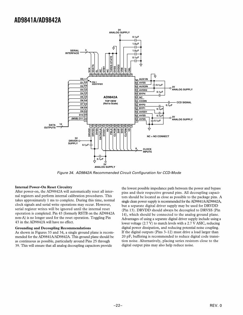
Internal Power-On Reset CircuitryAfter power-on, the AD9842A will automatically reset all inter-nal registers and perform internal calibration procedures. Thistakes approximately 1 ms to complete. During this time, normalclock signals and serial write operations may occur. However,serial register writes will be ignored until the internal resetoperation is completed. Pin 43 (formerly RSTB on the AD9842Anon-A) is no longer used for the reset operation. Toggling Pin43 in the AD9842A will have no effect.
Grounding and Decoupling RecommendationsAs shown in Figures 33 and 34, a single ground plane is recom-mended for the AD9841A/AD9842A. This ground plane should beas continuous as possible, particularly around Pins 25 through39. This will ensure that all analog decoupling capacitors provide
the lowest possible impedance path between the power and bypasspins and their respective ground pins. All decoupling capaci-tors should be located as close as possible to the package pins. Asingle clean power supply is recommended for the AD9841A/AD9842A,but a separate digital driver supply may be used for DRVDD(Pin 13). DRVDD should always be decoupled to DRVSS (Pin14), which should be connected to the analog ground plane.Advantages of using a separate digital driver supply include using alower voltage (2.7 V) to match levels with a 2.7 V ASIC, reducingdigital power dissipation, and reducing potential noise coupling.If the digital outputs (Pins 3–12) must drive a load larger than20 pF, buffering is recommended to reduce digital code transi-tion noise. Alternatively, placing series resistors close to thedigital output pins may also help reduce noise.
REV. 0
AD9841A/AD9842A
–23–
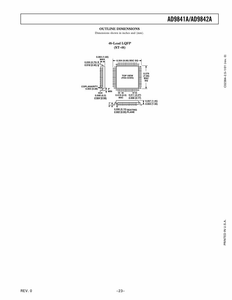
OUTLINE DIMENSIONSDimensions shown in inches and (mm).
48-Lead LQFP(ST-48)
TOP VIEW(PINS DOWN)
1
1213
2524
363748
0.019 (0.5)BSC
0.276(7.00)BSCSQ
0.011 (0.27)0.006 (0.17)
0.354 (9.00) BSC SQ
0.063 (1.60)MAX
0.030 (0.75)0.018 (0.45)
0.008 (0.2)0.004 (0.09)
0�MIN
COPLANARITY0.003 (0.08)
SEATINGPLANE
0.006 (0.15)0.002 (0.05)
7�0�
0.057 (1.45)0.053 (1.35)
C02
384–
2.5–
1/01
(re
v. 0
)P
RIN
TE
D IN
U.S
.A.